EP3410111A1 - Flexible sensor module and manufacturing method therefor - Google Patents
Flexible sensor module and manufacturing method therefor Download PDFInfo
- Publication number
- EP3410111A1 EP3410111A1 EP16888282.7A EP16888282A EP3410111A1 EP 3410111 A1 EP3410111 A1 EP 3410111A1 EP 16888282 A EP16888282 A EP 16888282A EP 3410111 A1 EP3410111 A1 EP 3410111A1
- Authority
- EP
- European Patent Office
- Prior art keywords
- solar cell
- substrate
- sensing unit
- metallic electrode
- sensor module
- Prior art date
- Legal status (The legal status is an assumption and is not a legal conclusion. Google has not performed a legal analysis and makes no representation as to the accuracy of the status listed.)
- Granted
Links
Images


Classifications
-
- H—ELECTRICITY
- H01—ELECTRIC ELEMENTS
- H01M—PROCESSES OR MEANS, e.g. BATTERIES, FOR THE DIRECT CONVERSION OF CHEMICAL ENERGY INTO ELECTRICAL ENERGY
- H01M10/00—Secondary cells; Manufacture thereof
- H01M10/42—Methods or arrangements for servicing or maintenance of secondary cells or secondary half-cells
- H01M10/46—Accumulators structurally combined with charging apparatus
- H01M10/465—Accumulators structurally combined with charging apparatus with solar battery as charging system
-
- G—PHYSICS
- G01—MEASURING; TESTING
- G01D—MEASURING NOT SPECIALLY ADAPTED FOR A SPECIFIC VARIABLE; ARRANGEMENTS FOR MEASURING TWO OR MORE VARIABLES NOT COVERED IN A SINGLE OTHER SUBCLASS; TARIFF METERING APPARATUS; MEASURING OR TESTING NOT OTHERWISE PROVIDED FOR
- G01D11/00—Component parts of measuring arrangements not specially adapted for a specific variable
- G01D11/30—Supports specially adapted for an instrument; Supports specially adapted for a set of instruments
-
- H—ELECTRICITY
- H02—GENERATION; CONVERSION OR DISTRIBUTION OF ELECTRIC POWER
- H02J—ELECTRIC POWER NETWORKS; CIRCUIT ARRANGEMENTS OR SYSTEMS FOR SUPPLYING OR DISTRIBUTING ELECTRIC POWER; SYSTEMS FOR STORING ELECTRIC ENERGY
- H02J7/00—Circuit arrangements for charging or discharging batteries or for supplying loads from batteries
- H02J7/34—Parallel operation in networks using both storage and other DC sources, e.g. providing buffering
- H02J7/35—Parallel operation in networks using both storage and other DC sources, e.g. providing buffering with light sensitive cells
-
- H—ELECTRICITY
- H04—ELECTRIC COMMUNICATION TECHNIQUE
- H04Q—SELECTING
- H04Q9/00—Arrangements in telecontrol or telemetry systems for selectively calling a substation from a main station, in which substation desired apparatus is selected for applying a control signal thereto or for obtaining measured values therefrom
-
- H—ELECTRICITY
- H10—SEMICONDUCTOR DEVICES; ELECTRIC SOLID-STATE DEVICES NOT OTHERWISE PROVIDED FOR
- H10F—INORGANIC SEMICONDUCTOR DEVICES SENSITIVE TO INFRARED RADIATION, LIGHT, ELECTROMAGNETIC RADIATION OF SHORTER WAVELENGTH OR CORPUSCULAR RADIATION
- H10F19/00—Integrated devices, or assemblies of multiple devices, comprising at least one photovoltaic cell covered by group H10F10/00, e.g. photovoltaic modules
- H10F19/80—Encapsulations or containers for integrated devices, or assemblies of multiple devices, having photovoltaic cells
-
- H—ELECTRICITY
- H10—SEMICONDUCTOR DEVICES; ELECTRIC SOLID-STATE DEVICES NOT OTHERWISE PROVIDED FOR
- H10F—INORGANIC SEMICONDUCTOR DEVICES SENSITIVE TO INFRARED RADIATION, LIGHT, ELECTROMAGNETIC RADIATION OF SHORTER WAVELENGTH OR CORPUSCULAR RADIATION
- H10F71/00—Manufacture or treatment of devices covered by this subclass
- H10F71/127—The active layers comprising only Group III-V materials, e.g. GaAs or InP
-
- H—ELECTRICITY
- H10—SEMICONDUCTOR DEVICES; ELECTRIC SOLID-STATE DEVICES NOT OTHERWISE PROVIDED FOR
- H10F—INORGANIC SEMICONDUCTOR DEVICES SENSITIVE TO INFRARED RADIATION, LIGHT, ELECTROMAGNETIC RADIATION OF SHORTER WAVELENGTH OR CORPUSCULAR RADIATION
- H10F77/00—Constructional details of devices covered by this subclass
- H10F77/20—Electrodes
- H10F77/206—Electrodes for devices having potential barriers
- H10F77/211—Electrodes for devices having potential barriers for photovoltaic cells
-
- H—ELECTRICITY
- H10—SEMICONDUCTOR DEVICES; ELECTRIC SOLID-STATE DEVICES NOT OTHERWISE PROVIDED FOR
- H10F—INORGANIC SEMICONDUCTOR DEVICES SENSITIVE TO INFRARED RADIATION, LIGHT, ELECTROMAGNETIC RADIATION OF SHORTER WAVELENGTH OR CORPUSCULAR RADIATION
- H10F77/00—Constructional details of devices covered by this subclass
- H10F77/90—Energy storage means directly associated or integrated with photovoltaic cells, e.g. capacitors integrated with photovoltaic cells
-
- H—ELECTRICITY
- H04—ELECTRIC COMMUNICATION TECHNIQUE
- H04Q—SELECTING
- H04Q2209/00—Arrangements in telecontrol or telemetry systems
- H04Q2209/40—Arrangements in telecontrol or telemetry systems using a wireless architecture
-
- H—ELECTRICITY
- H04—ELECTRIC COMMUNICATION TECHNIQUE
- H04Q—SELECTING
- H04Q2209/00—Arrangements in telecontrol or telemetry systems
- H04Q2209/80—Arrangements in the sub-station, i.e. sensing device
- H04Q2209/88—Providing power supply at the sub-station
- H04Q2209/886—Providing power supply at the sub-station using energy harvesting, e.g. solar, wind or mechanical
-
- H—ELECTRICITY
- H10—SEMICONDUCTOR DEVICES; ELECTRIC SOLID-STATE DEVICES NOT OTHERWISE PROVIDED FOR
- H10W—GENERIC PACKAGES, INTERCONNECTIONS, CONNECTORS OR OTHER CONSTRUCTIONAL DETAILS OF DEVICES COVERED BY CLASS H10
- H10W90/00—Package configurations
-
- Y—GENERAL TAGGING OF NEW TECHNOLOGICAL DEVELOPMENTS; GENERAL TAGGING OF CROSS-SECTIONAL TECHNOLOGIES SPANNING OVER SEVERAL SECTIONS OF THE IPC; TECHNICAL SUBJECTS COVERED BY FORMER USPC CROSS-REFERENCE ART COLLECTIONS [XRACs] AND DIGESTS
- Y02—TECHNOLOGIES OR APPLICATIONS FOR MITIGATION OR ADAPTATION AGAINST CLIMATE CHANGE
- Y02E—REDUCTION OF GREENHOUSE GAS [GHG] EMISSIONS, RELATED TO ENERGY GENERATION, TRANSMISSION OR DISTRIBUTION
- Y02E10/00—Energy generation through renewable energy sources
- Y02E10/50—Photovoltaic [PV] energy
-
- Y—GENERAL TAGGING OF NEW TECHNOLOGICAL DEVELOPMENTS; GENERAL TAGGING OF CROSS-SECTIONAL TECHNOLOGIES SPANNING OVER SEVERAL SECTIONS OF THE IPC; TECHNICAL SUBJECTS COVERED BY FORMER USPC CROSS-REFERENCE ART COLLECTIONS [XRACs] AND DIGESTS
- Y02—TECHNOLOGIES OR APPLICATIONS FOR MITIGATION OR ADAPTATION AGAINST CLIMATE CHANGE
- Y02E—REDUCTION OF GREENHOUSE GAS [GHG] EMISSIONS, RELATED TO ENERGY GENERATION, TRANSMISSION OR DISTRIBUTION
- Y02E10/00—Energy generation through renewable energy sources
- Y02E10/50—Photovoltaic [PV] energy
- Y02E10/544—Solar cells from Group III-V materials
-
- Y—GENERAL TAGGING OF NEW TECHNOLOGICAL DEVELOPMENTS; GENERAL TAGGING OF CROSS-SECTIONAL TECHNOLOGIES SPANNING OVER SEVERAL SECTIONS OF THE IPC; TECHNICAL SUBJECTS COVERED BY FORMER USPC CROSS-REFERENCE ART COLLECTIONS [XRACs] AND DIGESTS
- Y02—TECHNOLOGIES OR APPLICATIONS FOR MITIGATION OR ADAPTATION AGAINST CLIMATE CHANGE
- Y02E—REDUCTION OF GREENHOUSE GAS [GHG] EMISSIONS, RELATED TO ENERGY GENERATION, TRANSMISSION OR DISTRIBUTION
- Y02E60/00—Enabling technologies; Technologies with a potential or indirect contribution to GHG emissions mitigation
- Y02E60/10—Energy storage using batteries
-
- Y—GENERAL TAGGING OF NEW TECHNOLOGICAL DEVELOPMENTS; GENERAL TAGGING OF CROSS-SECTIONAL TECHNOLOGIES SPANNING OVER SEVERAL SECTIONS OF THE IPC; TECHNICAL SUBJECTS COVERED BY FORMER USPC CROSS-REFERENCE ART COLLECTIONS [XRACs] AND DIGESTS
- Y02—TECHNOLOGIES OR APPLICATIONS FOR MITIGATION OR ADAPTATION AGAINST CLIMATE CHANGE
- Y02P—CLIMATE CHANGE MITIGATION TECHNOLOGIES IN THE PRODUCTION OR PROCESSING OF GOODS
- Y02P70/00—Climate change mitigation technologies in the production process for final industrial or consumer products
- Y02P70/50—Manufacturing or production processes characterised by the final manufactured product
Definitions
- the present invention relates to a sensor module including a solar cell, and a method for manufacturing the same.
- a sensor module formed as various sensors are integrated with each other.
- the sensor module means an apparatus where a sensing unit, a power unit, a communication unit, etc. are integrated with each other.
- an additional energy source is required.
- a primary cell a chemical cell has been used.
- the chemical cell degrades a user's convenience since it requires periodic charging or replacements.
- a solar cell of high efficiency is required such that the solar cell is used as an energy source of the sensor module.
- the size of the sensor module may be increased. This may cause a restriction in an installation position of the sensor module.
- a sensor module having a novel structure where the sensor module does not have a size increase due to an integrated configuration, and where the sensor module is installable on a curved surface due to its flexible characteristic.
- an aspect of the detailed description is to provide a flexible sensor module having a solar cell for driving, the solar cell configured to supply energy to the flexible sensor module.
- Another aspect of the detailed description is to provide a new structure to integrate a flexible sensor module.
- Another aspect of the detailed description is to provide a method of manufacturing a flexible sensor module having such a structure.
- a flexible sensor module including: a sensing unit formed on a first substrate so as to be exposed to the outside, and configured to measure external environment information; a solar cell disposed on the first substrate together with the sensing unit, and configured to generate a power by receiving light; a wireless communication unit disposed at one side on the first substrate, and configured to transmit the information measured by the sensing unit to an external server; and a chemical cell disposed at another side on the first substrate, charged by receiving the power from the solar cell, and configured to supply the power to the sensing unit and the wireless communication unit, wherein the solar cell includes: a compound layer disposed on the second substrate, and configured to generate the power to be supplied to the sensing unit by receiving light; and a metallic electrode formed on the compound layer.
- the sensing unit, the solar cell, the wireless communication unit, and the chemical cell may be disposed at different positions on the first substrate.
- the solar cell may be disposed on at least one of the wireless communication unit and the chemical cell, in order to absorb light in an exposed state to the outside.
- the metallic electrode may connect the solar cell, the sensing unit, the wireless communication unit, and the chemical cell to each other.
- the metallic electrode may include: an upper metallic electrode formed on the compound layer; and a lower metallic electrode disposed between the second substrate and the compound layer, and disposed on an opposite side to the upper metallic electrode on the basis of the compound layer.
- the sensing unit may measure at least one of a temperature, a humidity, a gas concentration and an illuminance of the outside, in an exposed state to the outside.
- the compound layer may be formed as a layer of a compound of one element of group 3 and another element of group 5.
- the elements of group 3 and group 5 may be formed as gallium (Ga) and arsenic (As).
- a flexible sensor module including: a sensing unit formed on a first substrate, and configured to measure external environment information; a solar cell disposed on the first substrate together with the sensing unit; a wireless communication unit disposed on the first substrate together with the solar cell, and configured to transmit information measured by the sensing unit to an external server; and a chemical cell disposed on the first substrate together with the wireless communication unit, charged by receiving a power from the solar cell, and configured to supply the power to the sensing unit and the wireless communication unit, wherein the solar cell includes: a second substrate disposed to face the first substrate; a compound layer disposed on the second substrate, and configured to generate the power to be supplied to the sensing unit by receiving light; a metallic electrode formed on the compound layer; and one or more through holes formed to pass through upper and lower parts of the solar cell, such that the sensing unit is exposed to the outside.
- the metallic electrode may connect the solar cell, the sensing unit, the wireless communication unit, and the chemical cell to each other.
- the metallic electrode may include: an upper metallic electrode formed on the compound layer; and a lower metallic electrode disposed between the second substrate and the compound layer, and disposed on an opposite side to the upper metallic electrode on the basis of the compound layer.
- the solar cell may be disposed such that the second substrate, the lower metallic electrode, the compound layer and the upper metallic electrode are sequentially laminated, at both sides on the basis of the through hole, in a facing manner.
- the sensing unit may measure at least one of a temperature, a humidity, a gas concentration and an illuminance of the outside, in an exposed state to the outside via each of the through holes.
- the flexible sensor module may further include a sealing unit configured to cover the solar cell in order to prevent the solar cell from being exposed to the outside.
- the flexible sensor module may further include a signal amplifier formed on the first substrate together with the sensing unit, and configured to amplify a signal measured by the sensing unit.
- a method of manufacturing a flexible sensor module including: a first step of forming a half-finished product by laminating a sensing unit, a chemical cell and a wireless communication unit on a first substrate; and a second step of forming a solar cell, wherein the second step includes: forming a lower metallic electrode on a second substrate facing the first substrate; forming a compound layer of one element of group 3 and another element of group 5, on the lower metallic electrode; forming an upper metallic electrode on the compound layer of elements of groups 3, 5, such that part of the compound layer of elements of groups 3, 5 is exposed to the outside; and forming a through hole so as to pass through the second substrate, the lower metallic electrode, the compound layer of elements of groups 3, 5, and the upper metallic electrode which are laminated on each other, wherein the method further includes a third step of coupling the solar cell onto the half-finished product after firstly forming the half-finished
- the forming a through hole may include: a step of exposing the lower metallic electrode to the outside by removing part of the compound layer of elements of groups 3, 5 exposed to the outside; and a step of exposing the sensing unit to the outside by punching the lower metallic electrode and the second substrate.
- the method may further include a fourth step of covering the solar cell by a sealing unit, for prevention of contact between the solar cell coupled onto the half-finished product and air.
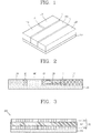
- FIG. 1 is a perspective view of a flexible sensor module 100
- FIG. 2 is a side sectional view illustrating a structure of the flexible sensor module 100 of FIG. 1 .
- the flexible sensor module 100 includes a sensing unit 110, a solar cell 120, a wireless communication unit 130 and a chemical cell 140. As shown in FIG. 1 , the components are laminated on the same substrate. Referring to FIG. 1 , the flexible sensor module 100 has a structure where the sensing unit 110, the solar cell 120, the wireless communication unit 130 and the chemical cell 140 are disposed on a first substrate 111.
- the flexible sensor module 100 is configured to collect external environment information by the sensing unit 110, and to transmit the information to the outside through the wireless communication unit 130. In a light environment, the flexible sensor module 100 executes the function by receiving a power through the solar cell 120. On the other hand, in a no-light environment, the flexible sensor module 100 is normally operated by storing part of a power generated by the solar cell 120 in the chemical cell 140.
- the sensing unit 110, the solar cell 120, the wireless communication unit 130 and the chemical cell 140 are disposed on the first substrate 111.
- the position and the arrangement state of the components may be variable. That is, the present invention is not limited to the structure and the arrangement state shown in FIG. 1 .
- the components may be positioned on the first substrate 111 in an arbitrary order, as long as they are positioned on the same substrate.
- the substrate of the present invention is configured to support the respective components, and to electrically connect the components to each other through connection lines formed thereon. Since the substrate of the present invention has a flexible characteristic, the flexible sensor module 100 may be mounted to a wall surface or a device each having a curved surface.
- the substrate includes a first substrate 111 and a second substrate 121.
- the first substrate 111 and the second substrate 121 are formed of a synthetic resin having a thickness less than 1mm, and have a bendable or flexible characteristic.
- the first substrate 111 and the second substrate 121 are not limited to this.
- FIG. 2 illustrates each component of the flexible sensor module 100.
- the components of the flexible sensor module 100, and a reciprocal operation thereof will be explained.
- the sensing unit 110 may be fixed onto the first substrate 111 through various means such as lead or a synthetic resin.
- the sensing unit 110 configured to measure external environment information, measures at least one of a temperature, a humidity, a gas concentration and an illuminance of the outside, in an exposed state to the outside.
- the sensing unit 110 may include at least one of a temperature sensor, a humidity sensor, a gas concentration measuring sensor and an illuminance sensor.
- the sensing unit 110 may be implemented as an integrated sensor of the respective sensors, or may be implemented as a plurality of different sensors.
- the sensing unit 110 may measure a gas concentration, a temperature, a humidity, an illuminance, etc. according to a usage purpose, and may execute various functions as a plurality of sensors are coupled thereto.
- the sensing unit 110 may have any structure and any shape. However, since the sensing unit 110 is implemented in the form of a module, it is preferable for the sensing unit 110 to include a flexible substrate.
- the sensing unit 110 is positioned so as to be exposed to the outside, since it should measure external environment information.
- the wireless communication unit 130 may be positioned at one side on the first substrate 111, or may be positioned on the same plane together with the sensing unit 110 disposed at one side on the first substrate 111.
- the wireless communication unit 130 configured to transmit information measured by the sensing unit 110 to an external server, may execute a wireless communication function by selecting a wide range of frequency of about 1.56MHz ⁇ 2.54GHz.
- Information about a temperature, a gas concentration, an illuminance, a humidity, etc. each measured by the sensing unit 110 may be transmitted to an external server through the wireless communication unit 130.
- a user may check the transmitted information through various devices such as a computer, a smart phone and a notebook.
- the wireless communication unit 130 may be formed to have a thickness less than 1mm for a flexible characteristic.
- the wireless communication unit 130 may be disposed at any position since it needs not be exposed to the outside. As shown in FIG. 2 , the wireless communication unit 130 is fixed at one side on the first substrate 111 by using lead, a synthetic resin, etc. That is, the wireless communication unit 130 is positioned on the same plane as the sensing unit 110.
- the chemical cell 140 configured to supply a power to each component of the flexible sensor module 100 by converting chemical energy into electric energy, may be implemented as a secondary cell including zinc (Zn), lithium (Li), etc.
- the chemical cell 140 may be formed to have a thickness less than 1mm for a flexible characteristic. In an environment where the solar cell 120 cannot generate a power, the chemical cell 140 supplies a power stored therein to the sensing unit 110 and the wireless communication unit 130 such that the sensing unit 110 and the wireless communication unit 130 are operated.
- the chemical cell 140 may be positioned at one side on the first substrate 111, and may be positioned on the same plane as the sensing unit 110 and the wireless communication unit 130.
- the chemical cell 140 is charged by receiving a power from the solar cell 120, and the power is used to operate the sensing unit 110 and the wireless communication unit 130, in a case where the solar cell 120 cannot absorb light to thus generate no power.
- the chemical cell 140 provides the power stored therein to the sensing unit 110 and the wireless communication unit 130 to operate them.
- the chemical cell 140 may be disposed at any position. Referring to FIG. 2 , the chemical cell 140 is disposed on the same plane as the sensing unit 110, the wireless communication unit 130 and the solar cell 120.
- the sensing unit 110, the wireless communication unit 130 and the solar cell 120 may be disposed at specific positions on the first substrate 111, as a bonding material 10 is interposed therebetween.
- FIGS. 3 and 4 illustrate a structure of the solar cell 120.
- the solar cell 120 serving to convert solar energy into electric energy, is configured to convert light energy generated from the sun into electric energy. As shown in FIGS. 1 and 2 , the solar cell 120 is positioned at one side on the first substrate 111, and is positioned on the same plane as the sensing unit 110, the wireless communication unit 130 and the chemical cell 140.
- the solar cell 120 includes a second substrate 121, a compound layer 123, and a metallic electrode 125.
- the second substrate 121 faces the first substrate 111.
- the second substrate 121 supports the compound layer 123 and the metallic electrode 125 thereon.
- the second substrate 121 is connected to the first substrate 111 through a copper electrode formed thereat, and is connected to the sensing unit 110, the chemical cell 140 and the wireless communication unit 130.
- the second substrate 121 has the same configuration as the first substrate 111.
- an upper metallic electrode 125a and a lower metallic electrode 125b of the solar cell 120 serve as an 'n' layer and a 'p' layer, respectively.
- the compound layer 123 is positioned on the second substrate 121, and generates a power by separating electrons and holes from each other by receiving light.
- the compound layer 123 is formed as a layer of a compound of one element of group 3 and another element of group 5. More specifically, the compound layer 123 is formed as one element of group 3 and another element of group 5 of the periodic table are combined to each other.
- Gallium (Ga) may be used as the element of group 3
- arsenic (As) may be used as the element of group 5.
- the compound layer 123 may be formed to have a thin film of a thickness less than about 3 ⁇ m, for a flexible characteristic.
- the solar cell 120 including Ga and As generates a large amount of electricity than the conventional Si-based solar cell. In this case, a higher power generation amount may be provided even in an environment where illuminance is low (e.g., 400 lux).
- the solar cell 120 including Ga and As may have high generation efficiency even at a small thickness less than 3 ⁇ m, and has a flexible characteristic due to its bending characteristic. Accordingly, the flexible sensor module may have a compact configuration and a small weight.
- the metallic electrode 125 is formed on the surface of the compound layer 123, and includes an upper metallic electrode 125a and a lower metallic electrode 125b.
- the upper metallic electrode 125a is disposed on the compound layer 123, and includes a finger 125a' (refer to FIG. 8 ) and a busbar 125a" (refer to FIG. 8 ).
- the lower metallic electrode 125b is disposed between the second substrate and the compound layer 123, and is disposed on an opposite side to the upper metallic electrode 125a on the basis of the compound layer 123.
- the upper metallic electrode 125a and the lower metallic electrode 125b serve as electrodes which form electrons and holes on front and rear surfaces of the compound layer 123, in order to collect charges formed by light.
- the upper metallic electrode 125a forms an 'n' layer
- the lower metallic electrode 125b forms a 'p' layer.
- the upper metallic electrode 125a and the lower metallic electrode 125b are formed by using a metallic paste.
- the upper metallic electrode 125a is formed by using an aluminum (Al) paste
- the lower metallic electrode 125b is formed by using a silver (Ag) paste.
- a photoelectric effect is generated by a reciprocal operation among the compound layer 123, the upper metallic electrode 125a and the lower metallic electrode 125b, and thus an electromotive force is generated.
- the generated electromotive force is stored in the chemical cell 140 or is connected to a device which requires a power.
- the photoelectric effect means generating electric charges by absorbing light.
- the flexible sensor module 100 may further include a sealing unit 150 configured to cover the solar cell 120 in order to prevent the solar cell 120 from being exposed to the outside.
- the sealing unit 150 is disposed on the solar cell 120.
- the sealing unit 150 may be formed of a transparent synthetic resin in order to prevent water penetration into the solar cell 120 or contamination of the solar cell 120 due to exposure of the solar cell 120 to the outside.
- the sealing unit 150 may be formed of a PVC material.
- FIG. 5 is a perspective view illustrating a flexible sensor module 100 according to another embodiment of the present invention.
- the flexible sensor module 100 includes a sensing unit 110, a solar cell 120, a wireless communication unit 130 and a chemical cell 140.
- the components are laminated on a substrate.
- the flexible sensor module 100 of FIG. 5 has a structure where other components are laminated on some components.
- the chemical cell 140 and the wireless communication unit 130 are disposed at a lower part of the flexible sensor module 100, and the sensing unit 110 and the solar cell 120 may be disposed on the chemical cell 140 and the wireless communication unit 130.
- the wireless communication unit 130 is disposed below the solar cell 120, and the chemical cell 140 is disposed below the sensing unit 110.
- the positions of the solar cell 120 and the sensing unit 110 may be interchanged with each other.
- the solar cell 120 and the sensing unit 110 should be positioned so as to be exposed to the outside, because the solar cell 120 should generate a power by absorbing light from the outside and the sensing unit 110 should measure external environment information.
- the chemical cell 140 and the wireless communication unit 130 need not be positioned so as to be exposed to the outside, because they can perform functions without being exposed to the outside. That is, the solar cell 120 may be positioned on at least one of the wireless communication unit 130 and the chemical cell 140, in order to absorb light in an exposed state to the outside. And the sensing unit 110 may be positioned on at least one of the wireless communication unit 130 and the chemical cell 140, in order to measure external environment information.
- FIG. 6 is a perspective view illustrating a flexible sensor module 100 according to another embodiment of the present invention, which shows a through hole 127.
- FIG. 7 illustrates a structure of a solar cell 120 having the through hole 127.
- the flexible sensor module 100 includes a sensing unit 110, a solar cell 120, a wireless communication unit 130 and a chemical cell 140.
- the components are laminated on a substrate.
- the sensing unit 110, the wireless communication unit 130 and the chemical cell 140 may be disposed on a first substrate 111, and the solar cell 120 may be disposed on the sensing unit 110, the wireless communication unit 130 and the chemical cell 140.
- Positions of the sensing unit 110, the wireless communication unit 130 and the chemical cell 140 are not limited to the positions of FIG. 6 . That is, the positions of the sensing unit 110, the wireless communication unit 130 and the chemical cell 140 may be interchanged with each other.
- the flexible sensor module 100 may be mounted to a wall surface or a device each having a curved surface.
- the sensing unit 110 is disposed on the first substrate 111.
- the sensing unit 110 is exposed to the outside via the through hole 127, thereby measuring at least one of a temperature, a humidity, a gas concentration and an illuminance of the outside. Explanations of the sensing unit 110 will be replaced by the aforementioned ones.
- the wireless communication unit 130 disposed on the first substrate 111, may be positioned on the same plane as the sensing unit 110 or below the sensing unit 110.
- the chemical cell 140 may be disposed on the same plane together with the sensing unit 110, or may be disposed below the sensing unit 110. As shown in FIG. 6 , the sensing unit 110, the wireless communication unit 130 and the chemical cell 140 are disposed on the first substrate 111.
- the sensing unit 110, the wireless communication unit 130 and the chemical cell 140 may be fixed to specific positions on the first substrate 111 by a bonding material 10 interposed therebetween.
- the solar cell 120 is disposed above the sensing unit 110, and the sensing unit 110 is exposed to the outside via the through hole 127 of the solar cell 120.
- the solar cell 120 includes a second substrate 121, a compound layer 123, a metallic electrode 125, and a through hole 127 formed to pass through them.
- the second substrate 121 is disposed to face the first substrate 111.
- the second substrate 121 supports the metallic electrode 125 and the compound layer 123 thereon.
- the second substrate 121 is configured to connect the sensing unit 110, the wireless communication unit 130 and the chemical cell 140 to each other through a copper electrode disposed thereat, the sensing unit 110, the wireless communication unit 130 and the chemical cell 140 disposed below the second substrate 121.
- the compound layer 123, disposed on the second substrate 121 is formed as a layer of a compound of one element of group 3 and another element of group 5.
- Gallium (Ga) may be used as an element of group 3
- arsenic (As) may be used as an element of group 5.
- the metallic electrode 125, formed on the compound layer 123 includes an upper metallic electrode 125a and a lower metallic electrode 125b.
- FIG. 8A illustrates that the upper metallic electrode 125a is formed around a sensor A exposed to the outside via the through hole 127
- FIG. 8B illustrates that the upper metallic electrode 125a is formed around sensors A, B and C exposed to the outside via the through hole 127.
- the upper metallic electrode 125a is disposed on the compound layer 123, and includes a finger 125a"and a busbar 125a'.
- the finger 125a" is indicated by a plurality of dotted lines which extend in a horizontal direction, and the busbar 125a'is indicated by a plurality of dotted lines which extend in a vertical direction and which are formed at two ends of the finger 125a".
- the finger 125a" contacts the compound layer 123 at a wide area, and receives a current generated from the compound layer 123.
- the busbar 125a' is connected to the finger 125a", and receives a current generated from the compound layer 123 through the finger 125a".
- the lower metallic electrode 125b is disposed between the second substrate and the compound layer 123, and is disposed on an opposite side to the upper metallic electrode 125a on the basis of the compound layer 123.
- the upper metallic electrode 125a and the lower metallic electrode 125b serve as electrodes which form electrons and holes on front and rear surfaces of the compound layer 123, in order to collect charges formed by light.
- the upper metallic electrode 125a forms an 'n' layer
- the lower metallic electrode 125b forms a 'p' layer.
- the upper metallic electrode 125a and the lower metallic electrode 125b are formed by using a metallic paste.
- the upper metallic electrode 125a is formed by using an aluminum (Al) paste
- the lower metallic electrode 125b is formed by using a silver (Ag) paste.
- the solar cell 120 is arranged such that the second substrate 121, the lower metallic electrode 125b, the compound layer 123 and the upper metallic electrode 125a are sequentially laminated, at both sides on the basis of the through hole 127, in a facing manner.
- the through hole 127 is formed to pass through upper and lower parts of the solar cell 120, such that the sensing unit 110 is exposed to the outside.
- the through hole 127 may have any shape if the sensing unit 110 is exposed to the outside therethrough.
- the sensing unit 110 may be exposed to the outside via the through hole 127 of the solar cell 120, and may measure external environment information.
- a dead area which may occur from the substrate may be minimized.
- the through hole 127 of the solar cell 120 may be formed at any position. However, the through hole 127 is preferably formed such that the sensing unit 110 is exposed to the outside via the through hole at a central region of the solar cell 120, since the metallic electrode 125 of the solar cell 120 should be formed in a symmetrical manner on the basis of the through hole 127 for high power generation efficiency.
- the solar cell 120, the sensing unit 110, the wireless communication unit 130 and the chemical cell 140 may be connected to each other through connection lines formed on the first and second substrates 111, 121. And the chemical cell 140 and the solar cell 120 supply a power to each of the components.
- the connection lines are generally formed of a metallic material, especially, copper.
- FIG. 9 is a conceptual view illustrating a connection state of the solar cell 120, the sensing unit 110, the wireless communication unit 130 and the chemical cell 130.
- the solar cell 120 is connected to the chemical cell 140, and the chemical cell 140 is configured to store therein a power generated from the solar cell 120.
- the solar cell 120 and the chemical cell 140 are connected to the sensing unit 110 and the wireless communication unit 130, respectively.
- the sensing unit 110 and the wireless communication unit 130 are provided with the power from the solar cell 120 in a light environment .
- the sensing unit 110 and the wireless communication unit 130 are provided with the power stored in the chemical cell 140 after being used to charge the chemical cell 140.
- the connection lines may be formed in plurality in number, such that the connected state of the components may be maintained even if one of the connection lines is disconnected.
- the flexible sensor module 100 may further include a signal amplifier (not shown) formed on the first substrate 111 together with the sensing unit 110 and the chemical cell 140, and configured to amplify a signal measured by the sensing unit 110.
- the signal amplifier (not shown) may have any structure and any shape.
- the flexible sensor module 100 may further include a sealing unit 150 configured to cover the solar cell 120 in order to prevent the solar cell 120 from being exposed to the outside. Explanations of the sealing unit 150 will be replaced by the aforementioned ones.
- the sensing unit 110 configured to measure external environment information in an exposed state to the outside, should not have its exposed state restricted due to the sealing unit 150. Accordingly, as shown in FIGS. 6 and 7 , the sealing unit 150 covers each component of the solar cell 120 with exposing the sensing unit 110 to the outside. Accordingly, as shown in FIGS. 8A and 8B , the sensing unit, exposed to the outside via the single through hole 127 of the solar cell 120, may measure external environment information.
- the flexible sensor module 100 may have an optimized configuration and high efficiency, since the sensing unit 110 is exposed to the outside via the through hole 127 of the solar cell 120. Further, the flexible sensor module 100 may be bent due to its flexible characteristic, and may be easily mounted even to a curved surface due to its small thickness.
- the sensing unit 110 may measure a gas concentration, an illuminance, a temperature, a humidity, etc. according to a type of a sensor mounted thereto, and may transmit the sensing information to a smart phone, a notebook, a tablet PC and a computer each having a reception function, through the wireless communication unit 130.
- FIG. 10 is a conceptual view illustrating a method of manufacturing the flexible sensor module 100 having the through hole 127.
- the method of FIG. 10 may be also applicable to manufacture the flexible sensor module 100 of FIG. 2 which is not provided with the through hole 127.
- the flexible sensor module 100 may be manufactured through first to fourth steps.
- the sensing unit 110, the chemical cell 140 and the wireless communication unit 130 are laminated on the first substrate 111, thereby forming a half-finished product (first step).
- the sensing unit 110, the chemical cell 140 and the wireless communication unit 130 are disposed on the same plane, and the bonding material 10 is interposed therebetween.
- the solar cell 120 is formed (second step).
- the second step includes forming the lower metallic electrode 125b on the second substrate 121, forming the compound layer 123 of elements of groups 3, 5 on the lower metallic electrode 125b, forming the upper metallic electrode 125a on the compound layer 123 of elements of groups 3, 5, and forming the through hole 127 so as to pass through the second substrate 121, the lower metallic electrode 125b, the compound layer 123 of elements of groups 3, 5 and the upper metallic electrode 125a.
- the forming the through hole 127 includes a step of exposing the lower metallic electrode 125b to the outside by removing part of the compound layer 123 of elements of groups 3, 5 exposed to the outside in a chemical manner, and a step of exposing the sensing unit 110 to the outside by punching the lower metallic electrode 125b and the second substrate 121.
- the forming the through hole 127 to expose the sensing unit 110 to the outside may be implemented by punching the lower metallic electrode 125b and the second substrate 121, using a laser, a cutter or a punch.
- the through hole 127 may be formed at the solar cell 120 by removing the compound layer 123 exposed between the upper metallic electrodes 125a in a chemical manner, and by punching the lower metallic electrode 125b and the second substrate 121, using a laser, a cutter or a punch.
- the solar cell 120 is coupled onto the half-finished product after firstly forming the half-finished product and then forming the solar cell 120, or the solar cell 120 is coupled onto the half-finished product after firstly forming the solar cell 120 and then forming the half-finished product.
- the third step of coupling the half-finished product with the solar cell 120 may mean coupling the solar cell 120 onto the half-finished product after firstly forming the half-finished product in the first step and then forming the solar cell 120 in the second step.
- the third step may mean coupling the solar cell 120 onto the half-finished product after firstly forming the solar cell 120 in the second step and then forming the half-finished product in the first step.
- the third step may mean coupling the solar cell 120 onto the half-finished product after simultaneously forming the half-finished product in the first step and the solar cell 120 in the second step.
- the sealing unit 150 is disposed to cover the solar cell 120, for prevention of contact between the solar cell 120 coupled onto the half-finished product and air (fourth step).
- the sealing unit 150 has the same characteristic as that of the flexible sensor module 100 aforementioned.
- the flexible sensor module 100 may be manufactured through the first to fourth steps shown in FIG. 10 .
- the present invention may have the following advantages.
- the flexible sensor module since the flexible sensor module includes the solar cell of high efficiency, it may be provided with energy for driving, from the solar cell. Further, the flexible sensor module may be mounted even to a curved surface, owing to its flexible characteristic.
- the flexible sensor module may have an integrated configuration and a smaller size through an enhanced structure thereof.
- the flexible sensor module having the through hole may execute its function without having a size increase, by exposing the sensing unit to the outside.
Landscapes
- Engineering & Computer Science (AREA)
- Life Sciences & Earth Sciences (AREA)
- Computer Networks & Wireless Communication (AREA)
- Chemical & Material Sciences (AREA)
- Power Engineering (AREA)
- Sustainable Development (AREA)
- Sustainable Energy (AREA)
- General Physics & Mathematics (AREA)
- Physics & Mathematics (AREA)
- Manufacturing & Machinery (AREA)
- General Chemical & Material Sciences (AREA)
- Electrochemistry (AREA)
- Chemical Kinetics & Catalysis (AREA)
- Testing Or Calibration Of Command Recording Devices (AREA)
- Health & Medical Sciences (AREA)
- Medicinal Chemistry (AREA)
- Food Science & Technology (AREA)
- Analytical Chemistry (AREA)
- Biochemistry (AREA)
- General Health & Medical Sciences (AREA)
- Immunology (AREA)
- Pathology (AREA)
- Combustion & Propulsion (AREA)
Abstract
Description
- The present invention relates to a sensor module including a solar cell, and a method for manufacturing the same.
- In order to enhance utilization of an apparatus for sensing various information such as a temperature, a humidity, a gas concentration and an illuminance, required is a sensor module formed as various sensors are integrated with each other. The sensor module means an apparatus where a sensing unit, a power unit, a communication unit, etc. are integrated with each other.
- In order to drive each sensor included in the sensor module, an additional energy source is required. As the additional energy source, a primary cell, a chemical cell has been used. However, the chemical cell degrades a user's convenience since it requires periodic charging or replacements. In order to solve such a problem, may be implemented a sensor module including a solar cell not requiring additional replacement or charging of energy. In this case, a solar cell of high efficiency is required such that the solar cell is used as an energy source of the sensor module. In the case where the sensor module has the solar cell therein, the size of the sensor module may be increased. This may cause a restriction in an installation position of the sensor module.
- Accordingly, required is a sensor module having a novel structure where the sensor module does not have a size increase due to an integrated configuration, and where the sensor module is installable on a curved surface due to its flexible characteristic.
- Therefore, an aspect of the detailed description is to provide a flexible sensor module having a solar cell for driving, the solar cell configured to supply energy to the flexible sensor module.
- Another aspect of the detailed description is to provide a new structure to integrate a flexible sensor module.
- Another aspect of the detailed description is to provide a method of manufacturing a flexible sensor module having such a structure.
- To achieve these and other advantages and in accordance with the purpose of this specification, as embodied and broadly described herein, there is provided a flexible sensor module, including: a sensing unit formed on a first substrate so as to be exposed to the outside, and configured to measure external environment information; a solar cell disposed on the first substrate together with the sensing unit, and configured to generate a power by receiving light; a wireless communication unit disposed at one side on the first substrate, and configured to transmit the information measured by the sensing unit to an external server; and a chemical cell disposed at another side on the first substrate, charged by receiving the power from the solar cell, and configured to supply the power to the sensing unit and the wireless communication unit, wherein the solar cell includes: a compound layer disposed on the second substrate, and configured to generate the power to be supplied to the sensing unit by receiving light; and a metallic electrode formed on the compound layer.
- In an embodiment of the present invention, the sensing unit, the solar cell, the wireless communication unit, and the chemical cell may be disposed at different positions on the first substrate.
- In an embodiment of the present invention, the solar cell may be disposed on at least one of the wireless communication unit and the chemical cell, in order to absorb light in an exposed state to the outside.
- In an embodiment of the present invention, the metallic electrode may connect the solar cell, the sensing unit, the wireless communication unit, and the chemical cell to each other. And the metallic electrode may include: an upper metallic electrode formed on the compound layer; and a lower metallic electrode disposed between the second substrate and the compound layer, and disposed on an opposite side to the upper metallic electrode on the basis of the compound layer.
- In an embodiment of the present invention, the sensing unit may measure at least one of a temperature, a humidity, a gas concentration and an illuminance of the outside, in an exposed state to the outside.
- In an embodiment of the present invention, the compound layer may be formed as a layer of a compound of one element of
group 3 and another element ofgroup 5. - In an embodiment of the present invention, the elements of
group 3 andgroup 5 may be formed as gallium (Ga) and arsenic (As). - According to another aspect of the present invention, there is provided a flexible sensor module, including: a sensing unit formed on a first substrate, and configured to measure external environment information; a solar cell disposed on the first substrate together with the sensing unit; a wireless communication unit disposed on the first substrate together with the solar cell, and configured to transmit information measured by the sensing unit to an external server; and a chemical cell disposed on the first substrate together with the wireless communication unit, charged by receiving a power from the solar cell, and configured to supply the power to the sensing unit and the wireless communication unit, wherein the solar cell includes: a second substrate disposed to face the first substrate; a compound layer disposed on the second substrate, and configured to generate the power to be supplied to the sensing unit by receiving light; a metallic electrode formed on the compound layer; and one or more through holes formed to pass through upper and lower parts of the solar cell, such that the sensing unit is exposed to the outside.
- In an embodiment of the present invention, the metallic electrode may connect the solar cell, the sensing unit, the wireless communication unit, and the chemical cell to each other. And the metallic electrode may include: an upper metallic electrode formed on the compound layer; and a lower metallic electrode disposed between the second substrate and the compound layer, and disposed on an opposite side to the upper metallic electrode on the basis of the compound layer.
- In an embodiment of the present invention, the solar cell may be disposed such that the second substrate, the lower metallic electrode, the compound layer and the upper metallic electrode are sequentially laminated, at both sides on the basis of the through hole, in a facing manner.
- In an embodiment of the present invention, the sensing unit may measure at least one of a temperature, a humidity, a gas concentration and an illuminance of the outside, in an exposed state to the outside via each of the through holes.
- In an embodiment of the present invention, the flexible sensor module may further include a sealing unit configured to cover the solar cell in order to prevent the solar cell from being exposed to the outside.
- In an embodiment of the present invention, the flexible sensor module may further include a signal amplifier formed on the first substrate together with the sensing unit, and configured to amplify a signal measured by the sensing unit.
- To achieve these and other advantages and in accordance with the purpose of this specification, as embodied and broadly described herein, there is also provided a method of manufacturing a flexible sensor module, the method including: a first step of forming a half-finished product by laminating a sensing unit, a chemical cell and a wireless communication unit on a first substrate; and a second step of forming a solar cell, wherein the second step includes: forming a lower metallic electrode on a second substrate facing the first substrate; forming a compound layer of one element of
group 3 and another element ofgroup 5, on the lower metallic electrode; forming an upper metallic electrode on the compound layer of elements ofgroups groups groups - In an embodiment of the present invention, the forming a through hole may include: a step of exposing the lower metallic electrode to the outside by removing part of the compound layer of elements of
groups - In an embodiment of the present invention, the method may further include a fourth step of covering the solar cell by a sealing unit, for prevention of contact between the solar cell coupled onto the half-finished product and air.
- Further scope of applicability of the present application will become more apparent from the detailed description given hereinafter. However, it should be understood that the detailed description and specific examples, while indicating preferred embodiments of the invention, are given by way of illustration only, since various changes and modifications within the spirit and scope of the invention will become apparent to those skilled in the art from the detailed description.
- The accompanying drawings, which are included to provide a further understanding of the invention and are incorporated in and constitute a part of this specification, illustrate exemplary embodiments and together with the description serve to explain the principles of the invention.
- In the drawings:
-
FIG. 1 is a perspective view of a flexible sensor module including a solar cell according to an embodiment of the present invention; -
FIG. 2 is a side sectional view illustrating a structure of the flexible sensor module ofFIG. 1 ; -
FIG. 3 is a side sectional view illustrating a structure of a solar cell; -
FIG. 4 is a side sectional view illustrating that a sealing unit covers the solar cell ofFIG. 3 from an upper side; -
FIG. 5 is a perspective view illustrating a flexible sensor module including a solar cell according to another embodiment of the present invention; -
FIG. 6 is a side sectional view of a flexible sensor module including a solar cell according to still another embodiment of the present invention; -
FIG. 7 is a side sectional view illustrating a structure of the solar cell included in the flexible sensor module ofFIG. 6 ; -
FIGS. 8A and 8B are conceptual views illustrating a sensing unit and an upper metallic electrode, exposed to the outside via a through hole ofFIG. 7 ; -
FIG. 9 is a conceptual view illustrating a connection state of components of a flexible sensor module; -
FIG. 10 is a conceptual view illustrating a method of manufacturing a flexible sensor module; and -
FIGS. 11A to 11D are flowcharts illustrating each step of a method of manufacturing a flexible sensor module. - Description will now be given in detail of preferred configurations of a flexible sensor module according to the present invention, with reference to the accompanying drawings.
- For the sake of brief description with reference to the drawings, the same or equivalent components will be provided with the same reference numbers, and description thereof will not be repeated. A singular expression in the specification includes a plural meaning unless it is contextually definitely represented.
-
FIG. 1 is a perspective view of aflexible sensor module 100, andFIG. 2 is a side sectional view illustrating a structure of theflexible sensor module 100 ofFIG. 1 . - The
flexible sensor module 100 includes asensing unit 110, asolar cell 120, awireless communication unit 130 and achemical cell 140. As shown inFIG. 1 , the components are laminated on the same substrate. Referring toFIG. 1 , theflexible sensor module 100 has a structure where thesensing unit 110, thesolar cell 120, thewireless communication unit 130 and thechemical cell 140 are disposed on afirst substrate 111. - The
flexible sensor module 100 is configured to collect external environment information by thesensing unit 110, and to transmit the information to the outside through thewireless communication unit 130. In a light environment, theflexible sensor module 100 executes the function by receiving a power through thesolar cell 120. On the other hand, in a no-light environment, theflexible sensor module 100 is normally operated by storing part of a power generated by thesolar cell 120 in thechemical cell 140. - The
sensing unit 110, thesolar cell 120, thewireless communication unit 130 and thechemical cell 140 are disposed on thefirst substrate 111. In this case, the position and the arrangement state of the components may be variable. That is, the present invention is not limited to the structure and the arrangement state shown inFIG. 1 . For instance, the components may be positioned on thefirst substrate 111 in an arbitrary order, as long as they are positioned on the same substrate. - The substrate of the present invention is configured to support the respective components, and to electrically connect the components to each other through connection lines formed thereon. Since the substrate of the present invention has a flexible characteristic, the
flexible sensor module 100 may be mounted to a wall surface or a device each having a curved surface. - The substrate includes a
first substrate 111 and asecond substrate 121. Thefirst substrate 111 and thesecond substrate 121 are formed of a synthetic resin having a thickness less than 1mm, and have a bendable or flexible characteristic. However, thefirst substrate 111 and thesecond substrate 121 are not limited to this. -
FIG. 2 illustrates each component of theflexible sensor module 100. The components of theflexible sensor module 100, and a reciprocal operation thereof will be explained. - The
sensing unit 110 may be fixed onto thefirst substrate 111 through various means such as lead or a synthetic resin. Thesensing unit 110, configured to measure external environment information, measures at least one of a temperature, a humidity, a gas concentration and an illuminance of the outside, in an exposed state to the outside. For this, thesensing unit 110 may include at least one of a temperature sensor, a humidity sensor, a gas concentration measuring sensor and an illuminance sensor. Alternatively, thesensing unit 110 may be implemented as an integrated sensor of the respective sensors, or may be implemented as a plurality of different sensors. - The
sensing unit 110 may measure a gas concentration, a temperature, a humidity, an illuminance, etc. according to a usage purpose, and may execute various functions as a plurality of sensors are coupled thereto. Thesensing unit 110 may have any structure and any shape. However, since thesensing unit 110 is implemented in the form of a module, it is preferable for thesensing unit 110 to include a flexible substrate. - As shown in
FIG. 2 , thesensing unit 110 is positioned so as to be exposed to the outside, since it should measure external environment information. - The
wireless communication unit 130 may be positioned at one side on thefirst substrate 111, or may be positioned on the same plane together with thesensing unit 110 disposed at one side on thefirst substrate 111. Thewireless communication unit 130, configured to transmit information measured by thesensing unit 110 to an external server, may execute a wireless communication function by selecting a wide range of frequency of about 1.56MHz ∼ 2.54GHz. Information about a temperature, a gas concentration, an illuminance, a humidity, etc. each measured by thesensing unit 110 may be transmitted to an external server through thewireless communication unit 130. And a user may check the transmitted information through various devices such as a computer, a smart phone and a notebook. - Preferably, the
wireless communication unit 130 may be formed to have a thickness less than 1mm for a flexible characteristic. Thewireless communication unit 130 may be disposed at any position since it needs not be exposed to the outside. As shown inFIG. 2 , thewireless communication unit 130 is fixed at one side on thefirst substrate 111 by using lead, a synthetic resin, etc. That is, thewireless communication unit 130 is positioned on the same plane as thesensing unit 110. - The
chemical cell 140, configured to supply a power to each component of theflexible sensor module 100 by converting chemical energy into electric energy, may be implemented as a secondary cell including zinc (Zn), lithium (Li), etc. Thechemical cell 140 may be formed to have a thickness less than 1mm for a flexible characteristic. In an environment where thesolar cell 120 cannot generate a power, thechemical cell 140 supplies a power stored therein to thesensing unit 110 and thewireless communication unit 130 such that thesensing unit 110 and thewireless communication unit 130 are operated. - The
chemical cell 140 may be positioned at one side on thefirst substrate 111, and may be positioned on the same plane as thesensing unit 110 and thewireless communication unit 130. Thechemical cell 140 is charged by receiving a power from thesolar cell 120, and the power is used to operate thesensing unit 110 and thewireless communication unit 130, in a case where thesolar cell 120 cannot absorb light to thus generate no power. - If the
solar cell 120 has a difficulty in operation in a no light environment, thechemical cell 140 provides the power stored therein to thesensing unit 110 and thewireless communication unit 130 to operate them. Thechemical cell 140 may be disposed at any position. Referring toFIG. 2 , thechemical cell 140 is disposed on the same plane as thesensing unit 110, thewireless communication unit 130 and thesolar cell 120. - As shown in
FIGS. 1 and 2 , thesensing unit 110, thewireless communication unit 130 and thesolar cell 120 may be disposed at specific positions on thefirst substrate 111, as abonding material 10 is interposed therebetween. -
FIGS. 3 and4 illustrate a structure of thesolar cell 120. - The
solar cell 120, serving to convert solar energy into electric energy, is configured to convert light energy generated from the sun into electric energy. As shown inFIGS. 1 and 2 , thesolar cell 120 is positioned at one side on thefirst substrate 111, and is positioned on the same plane as thesensing unit 110, thewireless communication unit 130 and thechemical cell 140. - The
solar cell 120 includes asecond substrate 121, acompound layer 123, and ametallic electrode 125. - Since the
solar cell 120 is disposed on thefirst substrate 111, thesecond substrate 121 faces thefirst substrate 111. Thesecond substrate 121 supports thecompound layer 123 and themetallic electrode 125 thereon. Thesecond substrate 121 is connected to thefirst substrate 111 through a copper electrode formed thereat, and is connected to thesensing unit 110, thechemical cell 140 and thewireless communication unit 130. Thesecond substrate 121 has the same configuration as thefirst substrate 111. - Once light is incident onto the
compound layer 123 of thesolar cell 120, electrons and holes are generated by light energy. In case of a p-type semiconductor device, a large number of carriers form holes, and a small number carriers form electrons. Electrons and holes are generated by light, and the generated electrons and holes spread to the periphery by a density difference therebetween. Once a potential difference reaches a p-n bonding unit, the electrons and the holes are separated from each other by a strong electric field. The electrons dispersed in the p-type semiconductor device move to an n-type semiconductor device, and the holes dispersed in the n-type semiconductor device move to the p-type semiconductor device. And power may be generated by a current flow principle. In the present invention, an uppermetallic electrode 125a and a lowermetallic electrode 125b of thesolar cell 120 serve as an 'n' layer and a 'p' layer, respectively. - The
compound layer 123 is positioned on thesecond substrate 121, and generates a power by separating electrons and holes from each other by receiving light. Thecompound layer 123 is formed as a layer of a compound of one element ofgroup 3 and another element ofgroup 5. More specifically, thecompound layer 123 is formed as one element ofgroup 3 and another element ofgroup 5 of the periodic table are combined to each other. Gallium (Ga) may be used as the element ofgroup 3, and arsenic (As) may be used as the element ofgroup 5. Thecompound layer 123 may be formed to have a thin film of a thickness less than about 3 µm, for a flexible characteristic. - The
solar cell 120 including Ga and As generates a large amount of electricity than the conventional Si-based solar cell. In this case, a higher power generation amount may be provided even in an environment where illuminance is low (e.g., 400 lux). - The
solar cell 120 including Ga and As may have high generation efficiency even at a small thickness less than 3 µm, and has a flexible characteristic due to its bending characteristic. Accordingly, the flexible sensor module may have a compact configuration and a small weight. - Referring to
FIGS. 3 and4 , themetallic electrode 125 is formed on the surface of thecompound layer 123, and includes an uppermetallic electrode 125a and a lowermetallic electrode 125b. - The upper
metallic electrode 125a is disposed on thecompound layer 123, and includes afinger 125a' (refer toFIG. 8 ) and abusbar 125a" (refer toFIG. 8 ). The lowermetallic electrode 125b is disposed between the second substrate and thecompound layer 123, and is disposed on an opposite side to the uppermetallic electrode 125a on the basis of thecompound layer 123. - The upper
metallic electrode 125a and the lowermetallic electrode 125b serve as electrodes which form electrons and holes on front and rear surfaces of thecompound layer 123, in order to collect charges formed by light. In the present invention, the uppermetallic electrode 125a forms an 'n' layer, and the lowermetallic electrode 125b forms a 'p' layer. - The upper
metallic electrode 125a and the lowermetallic electrode 125b are formed by using a metallic paste. The uppermetallic electrode 125a is formed by using an aluminum (Al) paste, and the lowermetallic electrode 125b is formed by using a silver (Ag) paste. - Once solar energy is irradiated to the
solar cell 120, a photoelectric effect is generated by a reciprocal operation among thecompound layer 123, the uppermetallic electrode 125a and the lowermetallic electrode 125b, and thus an electromotive force is generated. The generated electromotive force is stored in thechemical cell 140 or is connected to a device which requires a power. The photoelectric effect means generating electric charges by absorbing light. - As shown in
FIG. 4 , theflexible sensor module 100 may further include asealing unit 150 configured to cover thesolar cell 120 in order to prevent thesolar cell 120 from being exposed to the outside. The sealingunit 150 is disposed on thesolar cell 120. The sealingunit 150 may be formed of a transparent synthetic resin in order to prevent water penetration into thesolar cell 120 or contamination of thesolar cell 120 due to exposure of thesolar cell 120 to the outside. For instance, the sealingunit 150 may be formed of a PVC material. -
FIG. 5 is a perspective view illustrating aflexible sensor module 100 according to another embodiment of the present invention. - The
flexible sensor module 100 includes asensing unit 110, asolar cell 120, awireless communication unit 130 and achemical cell 140. The components are laminated on a substrate. Unlike theflexible sensor module 100 where the components are disposed on the same plane, theflexible sensor module 100 ofFIG. 5 has a structure where other components are laminated on some components. - As shown in
FIG. 5 , thechemical cell 140 and thewireless communication unit 130 are disposed at a lower part of theflexible sensor module 100, and thesensing unit 110 and thesolar cell 120 may be disposed on thechemical cell 140 and thewireless communication unit 130. - Referring to
FIG. 5 , thewireless communication unit 130 is disposed below thesolar cell 120, and thechemical cell 140 is disposed below thesensing unit 110. The positions of thesolar cell 120 and thesensing unit 110 may be interchanged with each other. However, thesolar cell 120 and thesensing unit 110 should be positioned so as to be exposed to the outside, because thesolar cell 120 should generate a power by absorbing light from the outside and thesensing unit 110 should measure external environment information. Thechemical cell 140 and thewireless communication unit 130 need not be positioned so as to be exposed to the outside, because they can perform functions without being exposed to the outside. That is, thesolar cell 120 may be positioned on at least one of thewireless communication unit 130 and thechemical cell 140, in order to absorb light in an exposed state to the outside. And thesensing unit 110 may be positioned on at least one of thewireless communication unit 130 and thechemical cell 140, in order to measure external environment information. -
FIG. 6 is a perspective view illustrating aflexible sensor module 100 according to another embodiment of the present invention, which shows a throughhole 127. AndFIG. 7 illustrates a structure of asolar cell 120 having the throughhole 127. - The
flexible sensor module 100 includes asensing unit 110, asolar cell 120, awireless communication unit 130 and achemical cell 140. The components are laminated on a substrate. Thesensing unit 110, thewireless communication unit 130 and thechemical cell 140 may be disposed on afirst substrate 111, and thesolar cell 120 may be disposed on thesensing unit 110, thewireless communication unit 130 and thechemical cell 140. Positions of thesensing unit 110, thewireless communication unit 130 and thechemical cell 140 are not limited to the positions ofFIG. 6 . That is, the positions of thesensing unit 110, thewireless communication unit 130 and thechemical cell 140 may be interchanged with each other. - Since the substrate of the
flexible sensor module 100 has a flexible characteristic, theflexible sensor module 100 may be mounted to a wall surface or a device each having a curved surface. - The
sensing unit 110 is disposed on thefirst substrate 111. Thesensing unit 110 is exposed to the outside via the throughhole 127, thereby measuring at least one of a temperature, a humidity, a gas concentration and an illuminance of the outside. Explanations of thesensing unit 110 will be replaced by the aforementioned ones. - The
wireless communication unit 130, disposed on thefirst substrate 111, may be positioned on the same plane as thesensing unit 110 or below thesensing unit 110. Thechemical cell 140 may be disposed on the same plane together with thesensing unit 110, or may be disposed below thesensing unit 110. As shown inFIG. 6 , thesensing unit 110, thewireless communication unit 130 and thechemical cell 140 are disposed on thefirst substrate 111. Thesensing unit 110, thewireless communication unit 130 and thechemical cell 140 may be fixed to specific positions on thefirst substrate 111 by abonding material 10 interposed therebetween. - As shown in
FIGS. 6 and 7 , thesolar cell 120 is disposed above thesensing unit 110, and thesensing unit 110 is exposed to the outside via the throughhole 127 of thesolar cell 120. Thesolar cell 120 includes asecond substrate 121, acompound layer 123, ametallic electrode 125, and a throughhole 127 formed to pass through them. - The
second substrate 121 is disposed to face thefirst substrate 111. Thesecond substrate 121 supports themetallic electrode 125 and thecompound layer 123 thereon. Thesecond substrate 121 is configured to connect thesensing unit 110, thewireless communication unit 130 and thechemical cell 140 to each other through a copper electrode disposed thereat, thesensing unit 110, thewireless communication unit 130 and thechemical cell 140 disposed below thesecond substrate 121. Thecompound layer 123, disposed on thesecond substrate 121, is formed as a layer of a compound of one element ofgroup 3 and another element ofgroup 5. Gallium (Ga) may be used as an element ofgroup 3, and arsenic (As) may be used as an element ofgroup 5. Themetallic electrode 125, formed on thecompound layer 123, includes an uppermetallic electrode 125a and a lowermetallic electrode 125b. -
FIG. 8A illustrates that the uppermetallic electrode 125a is formed around a sensor A exposed to the outside via the throughhole 127, andFIG. 8B illustrates that the uppermetallic electrode 125a is formed around sensors A, B and C exposed to the outside via the throughhole 127. - The upper
metallic electrode 125a is disposed on thecompound layer 123, and includes afinger 125a"and abusbar 125a'. Thefinger 125a" is indicated by a plurality of dotted lines which extend in a horizontal direction, and the busbar 125a'is indicated by a plurality of dotted lines which extend in a vertical direction and which are formed at two ends of thefinger 125a". Thefinger 125a"contacts thecompound layer 123 at a wide area, and receives a current generated from thecompound layer 123. The busbar 125a'is connected to thefinger 125a", and receives a current generated from thecompound layer 123 through thefinger 125a". - The lower
metallic electrode 125b is disposed between the second substrate and thecompound layer 123, and is disposed on an opposite side to the uppermetallic electrode 125a on the basis of thecompound layer 123. - The upper
metallic electrode 125a and the lowermetallic electrode 125b serve as electrodes which form electrons and holes on front and rear surfaces of thecompound layer 123, in order to collect charges formed by light. In the present invention, the uppermetallic electrode 125a forms an 'n' layer, and the lowermetallic electrode 125b forms a 'p' layer. - The upper
metallic electrode 125a and the lowermetallic electrode 125b are formed by using a metallic paste. The uppermetallic electrode 125a is formed by using an aluminum (Al) paste, and the lowermetallic electrode 125b is formed by using a silver (Ag) paste. - Once solar energy is irradiated to the
solar cell 120, a photoelectric effect is generated by a reciprocal operation among thecompound layer 123, the uppermetallic electrode 125a and the lowermetallic electrode 125b, and thus an electromotive force is generated. The generated electromotive force is stored in thechemical cell 140 or is connected to a device which requires a power. - As shown in
FIG. 7 , thesolar cell 120 is arranged such that thesecond substrate 121, the lowermetallic electrode 125b, thecompound layer 123 and the uppermetallic electrode 125a are sequentially laminated, at both sides on the basis of the throughhole 127, in a facing manner. The throughhole 127 is formed to pass through upper and lower parts of thesolar cell 120, such that thesensing unit 110 is exposed to the outside. The throughhole 127 may have any shape if thesensing unit 110 is exposed to the outside therethrough. - The
sensing unit 110 may be exposed to the outside via the throughhole 127 of thesolar cell 120, and may measure external environment information. In the case of forming thesensing unit 110 under thesolar cell 120 and exposing thesensing unit 110 via the throughhole 127, it is more advantageous in the aspect of module arrangement and space utilization, than in a case of forming thesensing unit 110 on thesolar cell 120. Further, in case of using a single substrate, a dead area which may occur from the substrate may be minimized. - The through
hole 127 of thesolar cell 120 may be formed at any position. However, the throughhole 127 is preferably formed such that thesensing unit 110 is exposed to the outside via the through hole at a central region of thesolar cell 120, since themetallic electrode 125 of thesolar cell 120 should be formed in a symmetrical manner on the basis of the throughhole 127 for high power generation efficiency. - The
solar cell 120, thesensing unit 110, thewireless communication unit 130 and thechemical cell 140 may be connected to each other through connection lines formed on the first andsecond substrates chemical cell 140 and thesolar cell 120 supply a power to each of the components. The connection lines are generally formed of a metallic material, especially, copper. -
FIG. 9 is a conceptual view illustrating a connection state of thesolar cell 120, thesensing unit 110, thewireless communication unit 130 and thechemical cell 130. - Referring to
FIG. 9 , thesolar cell 120 is connected to thechemical cell 140, and thechemical cell 140 is configured to store therein a power generated from thesolar cell 120. Thesolar cell 120 and thechemical cell 140 are connected to thesensing unit 110 and thewireless communication unit 130, respectively. Thesensing unit 110 and thewireless communication unit 130 are provided with the power from thesolar cell 120 in a light environment . On the other hand, in a no-light environment, thesensing unit 110 and thewireless communication unit 130 are provided with the power stored in thechemical cell 140 after being used to charge thechemical cell 140. Referring toFIG. 9 , the connection lines may be formed in plurality in number, such that the connected state of the components may be maintained even if one of the connection lines is disconnected. - The
flexible sensor module 100 may further include a signal amplifier (not shown) formed on thefirst substrate 111 together with thesensing unit 110 and thechemical cell 140, and configured to amplify a signal measured by thesensing unit 110. The signal amplifier (not shown) may have any structure and any shape. - The
flexible sensor module 100 may further include asealing unit 150 configured to cover thesolar cell 120 in order to prevent thesolar cell 120 from being exposed to the outside. Explanations of thesealing unit 150 will be replaced by the aforementioned ones. - The
sensing unit 110, configured to measure external environment information in an exposed state to the outside, should not have its exposed state restricted due to thesealing unit 150. Accordingly, as shown inFIGS. 6 and 7 , the sealingunit 150 covers each component of thesolar cell 120 with exposing thesensing unit 110 to the outside. Accordingly, as shown inFIGS. 8A and 8B , the sensing unit, exposed to the outside via the single throughhole 127 of thesolar cell 120, may measure external environment information. - The
flexible sensor module 100 may have an optimized configuration and high efficiency, since thesensing unit 110 is exposed to the outside via the throughhole 127 of thesolar cell 120. Further, theflexible sensor module 100 may be bent due to its flexible characteristic, and may be easily mounted even to a curved surface due to its small thickness. Thesensing unit 110 may measure a gas concentration, an illuminance, a temperature, a humidity, etc. according to a type of a sensor mounted thereto, and may transmit the sensing information to a smart phone, a notebook, a tablet PC and a computer each having a reception function, through thewireless communication unit 130. - So far, the structure of the
flexible sensor module 100 and the operation of each component have been explained. Hereinafter, a method of manufacturing theflexible sensor module 100 having the throughhole 127 will be explained with reference toFIG. 10 andFIGS. 11A to 11D . -
FIG. 10 is a conceptual view illustrating a method of manufacturing theflexible sensor module 100 having the throughhole 127. The method ofFIG. 10 may be also applicable to manufacture theflexible sensor module 100 ofFIG. 2 which is not provided with the throughhole 127. - The
flexible sensor module 100 may be manufactured through first to fourth steps. - Referring to
FIG. 10 (the upper left drawing) andFIG. 11A , thesensing unit 110, thechemical cell 140 and thewireless communication unit 130 are laminated on thefirst substrate 111, thereby forming a half-finished product (first step). As aforementioned with reference toFIG. 6 , thesensing unit 110, thechemical cell 140 and thewireless communication unit 130 are disposed on the same plane, and thebonding material 10 is interposed therebetween. - Referring to
FIG. 10 (the upper right drawing) andFIG. 11B , thesolar cell 120 is formed (second step). The second step includes forming the lowermetallic electrode 125b on thesecond substrate 121, forming thecompound layer 123 of elements ofgroups metallic electrode 125b, forming the uppermetallic electrode 125a on thecompound layer 123 of elements ofgroups hole 127 so as to pass through thesecond substrate 121, the lowermetallic electrode 125b, thecompound layer 123 of elements ofgroups metallic electrode 125a. - As shown in
FIG. 10 , the forming the throughhole 127 includes a step of exposing the lowermetallic electrode 125b to the outside by removing part of thecompound layer 123 of elements ofgroups sensing unit 110 to the outside by punching the lowermetallic electrode 125b and thesecond substrate 121. The forming the throughhole 127 to expose thesensing unit 110 to the outside may be implemented by punching the lowermetallic electrode 125b and thesecond substrate 121, using a laser, a cutter or a punch. - That is, the through
hole 127 may be formed at thesolar cell 120 by removing thecompound layer 123 exposed between the uppermetallic electrodes 125a in a chemical manner, and by punching the lowermetallic electrode 125b and thesecond substrate 121, using a laser, a cutter or a punch. - Referring to
FIGS. 10 and11C , thesolar cell 120 is coupled onto the half-finished product after firstly forming the half-finished product and then forming thesolar cell 120, or thesolar cell 120 is coupled onto the half-finished product after firstly forming thesolar cell 120 and then forming the half-finished product. - The third step of coupling the half-finished product with the
solar cell 120 may mean coupling thesolar cell 120 onto the half-finished product after firstly forming the half-finished product in the first step and then forming thesolar cell 120 in the second step. Alternatively, the third step may mean coupling thesolar cell 120 onto the half-finished product after firstly forming thesolar cell 120 in the second step and then forming the half-finished product in the first step. Still alternatively, the third step may mean coupling thesolar cell 120 onto the half-finished product after simultaneously forming the half-finished product in the first step and thesolar cell 120 in the second step. - Referring to
FIGS. 10 and11D , the sealingunit 150 is disposed to cover thesolar cell 120, for prevention of contact between thesolar cell 120 coupled onto the half-finished product and air (fourth step). The sealingunit 150 has the same characteristic as that of theflexible sensor module 100 aforementioned. - The
flexible sensor module 100 may be manufactured through the first to fourth steps shown inFIG. 10 . - The configurations and methods of the flexible sensor module and the method of manufacturing the same in the aforesaid embodiments may not be limitedly applied, but such embodiments may be configured by a selective combination of all or part of the embodiments so as to implement many variations.
- The present invention may have the following advantages.
- Firstly, since the flexible sensor module includes the solar cell of high efficiency, it may be provided with energy for driving, from the solar cell. Further, the flexible sensor module may be mounted even to a curved surface, owing to its flexible characteristic.
- Further, the flexible sensor module may have an integrated configuration and a smaller size through an enhanced structure thereof.
- Further, the flexible sensor module having the through hole may execute its function without having a size increase, by exposing the sensing unit to the outside.
- The configurations and methods of the mobile terminal in the aforesaid embodiments may not be limitedly applied, but such embodiments may be configured by a selective combination of all or part of the embodiments so as to implement many variations.
Claims (16)
- A flexible sensor module, comprising:a sensing unit formed on a first substrate to be exposed to the outside so as to measure external environment information;a solar cell disposed to be aligned with the sensing unit, and configured to generate a power by receiving light;a wireless communication unit disposed at one part on the first substrate, and configured to transmit the information measured by the sensing unit to an external server; anda chemical cell disposed at another part on the first substrate, charged by receiving the power from the solar cell, and configured to supply charged power to the sensing unit and the wireless communication unit,wherein the solar cell includes:a compound layer disposed on a second substrate, and configured to generate the power to be supplied to the sensing unit by receiving light; anda metallic electrode formed on a surface of the compound layer.
- The flexible sensor module of claim 1, wherein the sensing unit, the solar cell, the wireless communication unit, and the chemical cell are disposed at different positions on the first substrate.
- The flexible sensor module of claim 1, wherein the solar cell is disposed on at least one of the wireless communication unit and the chemical cell, in order to absorb light in an exposed state to the outside.
- The flexible sensor module of claim 1, wherein the metallic electrode connects the solar cell, the sensing unit, the wireless communication unit, and the chemical cell to each other, and
wherein the metallic electrode includes:an upper metallic electrode formed on the compound layer; anda lower metallic electrode disposed between the second substrate and the compound layer, and disposed on an opposite side to the upper metallic electrode on the basis of the compound layer. - The flexible sensor module of claim 1, wherein the sensing unit measures at least one of a temperature, a humidity, a gas concentration and an illuminance of the outside, in an exposed state to the outside.
- The flexible sensor module of claim 5, wherein the compound layer is formed as a layer of a compound of one element of group 3 and another element of group 5.
- The flexible sensor module of claim 6, wherein the elements of group 3 and group 5 are formed as gallium (Ga) and arsenic (As).
- A flexible sensor module, comprising:a sensing unit formed on a first substrate, and configured to measure external environment information;a solar cell disposed on the sensing unit;a wireless communication unit disposed on the first substrate together with the solar cell, and configured to transmit information measured by the sensing unit to an external server; anda chemical cell disposed on the first substrate together with the wireless communication unit, charged by receiving a power from the solar cell, and configured to supply the power to the sensing unit and the wireless communication unit,wherein the solar cell includes:a second substrate disposed to face the first substrate;a compound layer disposed on the second substrate, and configured to generate the power to be supplied to the sensing unit by receiving light;a metallic electrode formed on the compound layer; andone or more through holes formed to pass through upper and lower parts of the solar cell, such that the sensing unit is exposed to the outside.
- The flexible sensor module of claim 8, wherein the metallic electrode connects the solar cell, the sensing unit, the wireless communication unit, and the chemical cell to each other, and
wherein the metallic electrode includes:an upper metallic electrode formed on the compound layer; anda lower metallic electrode disposed between the second substrate and the compound layer, and disposed on an opposite side to the upper metallic electrode on the basis of the compound layer. - The flexible sensor module of claim 8, wherein the solar cell is disposed such that the second substrate, the lower metallic electrode, the compound layer and the upper metallic electrode are sequentially laminated, at both sides on the basis of the through hole, in a facing manner.
- The flexible sensor module of claim 8, wherein the sensing unit measures at least one of a temperature, a humidity, a gas concentration and an illuminance of the outside, in an exposed state to the outside via each of the through holes.
- The flexible sensor module of claim 8, further comprising a sealing unit configured to cover the solar cell in order to prevent the solar cell from being exposed to the outside.
- The flexible sensor module of claim 8, further comprising a signal amplifier formed on the first substrate together with the sensing unit, and configured to amplify a signal measured by the sensing unit.
- A method of manufacturing a flexible sensor module, the method comprising:a first step of forming a half-finished product by laminating a sensing unit, a chemical cell and a wireless communication unit on a first substrate; anda second step of forming a solar cell,wherein the second step includes:forming a lower metallic electrode on a second substrate facing the first substrate;forming a compound layer of one element of group 3 and another element of group 5, on the lower metallic electrode;forming an upper metallic electrode on the compound layer of elements of groups 3, 5, such that part of the compound layer of elements of groups 3, 5 is exposed to the outside; andforming a through hole so as to pass through the second substrate, the lower metallic electrode, the compound layer of elements of groups 3, 5, and the upper metallic electrode which are laminated on each other,wherein the method further includes a third step of coupling the solar cell onto the half-finished product after firstly forming the half-finished product and then forming the solar cell, or after firstly forming the solar cell and then forming the half-finished product.
- The method of claim 14, wherein the forming a through hole includes:a step of exposing the lower metallic electrode to the outside by removing part of the compound layer of elements of groups 3, 5 exposed to the outside; anda step of exposing the sensing unit to the outside by punching the lower metallic electrode and the second substrate.
- The method of claim 15, further comprising a fourth step of covering the solar cell by a sealing unit, for prevention of contact between the solar cell coupled onto the half-finished product and air.
Applications Claiming Priority (2)
| Application Number | Priority Date | Filing Date | Title |
|---|---|---|---|
| KR1020160009628A KR20170089340A (en) | 2016-01-26 | 2016-01-26 | Flexible sensor module and manufacturing method thereof |
| PCT/KR2016/008681 WO2017131306A1 (en) | 2016-01-26 | 2016-08-08 | Flexible sensor module and manufacturing method therefor |
Publications (3)
| Publication Number | Publication Date |
|---|---|
| EP3410111A1 true EP3410111A1 (en) | 2018-12-05 |
| EP3410111A4 EP3410111A4 (en) | 2019-06-26 |
| EP3410111B1 EP3410111B1 (en) | 2020-06-10 |
Family
ID=59359862
Family Applications (1)
| Application Number | Title | Priority Date | Filing Date |
|---|---|---|---|
| EP16888282.7A Active EP3410111B1 (en) | 2016-01-26 | 2016-08-08 | Flexible sensor module and manufacturing method therefor |
Country Status (4)
| Country | Link |
|---|---|
| US (1) | US10164299B2 (en) |
| EP (1) | EP3410111B1 (en) |
| KR (1) | KR20170089340A (en) |
| WO (1) | WO2017131306A1 (en) |
Families Citing this family (6)
| Publication number | Priority date | Publication date | Assignee | Title |
|---|---|---|---|---|
| US10389184B2 (en) * | 2016-08-31 | 2019-08-20 | Intel Corporation | Data transfer using beamed power |
| KR102267913B1 (en) | 2019-06-27 | 2021-06-23 | 세메스 주식회사 | Apparatus for treating substrate |
| CN114885615A (en) * | 2019-10-02 | 2022-08-09 | 纳博特斯克有限公司 | Sensor device, retarder, running unit for crawler, fluid valve, fluid cylinder, fluid pump, fluid compressor, electric motor, electric actuator, structure, method performed by sensor device, sensor system, and sign |
| US20220159354A1 (en) * | 2020-11-13 | 2022-05-19 | The Boeing Company | Internet of things label for factory and warehouse applications |
| KR102616022B1 (en) * | 2022-04-15 | 2023-12-20 | (주)파트론 | Optical sensor package |
| WO2025073022A1 (en) * | 2023-10-02 | 2025-04-10 | Virgilio Silva Charles | Structural arrangement for a multi-layer photovoltaic module, composed of laminated cells and batteries, for use in panels and/or tiles |
Family Cites Families (10)
| Publication number | Priority date | Publication date | Assignee | Title |
|---|---|---|---|---|
| WO2001073883A2 (en) * | 2000-03-24 | 2001-10-04 | Cymbet Corporation | Low-temperature fabrication of thin-film energy-storage devices |
| JP5398908B2 (en) * | 2009-05-27 | 2014-01-29 | コーニンクレッカ フィリップス エヌ ヴェ | Sensor used |
| KR20110061074A (en) * | 2009-12-01 | 2011-06-09 | 주식회사 티모테크놀로지 | Ventilation system using dye-sensitized solar cell |
| US9471070B2 (en) * | 2011-01-10 | 2016-10-18 | Shey Sabripour | Environmental control system including distributed control elements |
| JP2013122718A (en) * | 2011-12-12 | 2013-06-20 | Ngk Spark Plug Co Ltd | Radio sensor node |
| KR101412665B1 (en) * | 2012-03-30 | 2014-07-02 | 주식회사동일기술공사 | Road state sesing device and road-surrounding monitoring system using the same |
| KR20150080824A (en) * | 2014-01-02 | 2015-07-10 | 주식회사 안테크 | Indoor environment control system using solar energy |
| KR20150140183A (en) * | 2014-06-05 | 2015-12-15 | 정태훈 | Sensor Module Including Solar cell |
| US20160270220A1 (en) * | 2015-03-12 | 2016-09-15 | Kabushiki Kaisha Toshiba | Electronic apparatus |
| EP3271946A4 (en) * | 2015-03-19 | 2019-12-04 | Specmat Inc. | SILICON-CONTAINING SEMICONDUCTOR STRUCTURES, METHODS OF MANUFACTURING THE SAME, AND DEVICES COMPRISING SAME |
-
2016
- 2016-01-26 KR KR1020160009628A patent/KR20170089340A/en not_active Ceased
- 2016-08-08 WO PCT/KR2016/008681 patent/WO2017131306A1/en not_active Ceased
- 2016-08-08 EP EP16888282.7A patent/EP3410111B1/en active Active
- 2016-10-03 US US15/284,051 patent/US10164299B2/en active Active
Also Published As
| Publication number | Publication date |
|---|---|
| KR20170089340A (en) | 2017-08-03 |
| US10164299B2 (en) | 2018-12-25 |
| EP3410111A4 (en) | 2019-06-26 |
| EP3410111B1 (en) | 2020-06-10 |
| US20170214100A1 (en) | 2017-07-27 |
| WO2017131306A1 (en) | 2017-08-03 |
Similar Documents
| Publication | Publication Date | Title |
|---|---|---|
| EP3410111B1 (en) | Flexible sensor module and manufacturing method therefor | |
| JP2009081160A (en) | Solar cell and electronic device | |
| KR20110030376A (en) | Solar module board and solar module | |
| US20170331425A1 (en) | Portable photovoltaic system | |
| US20100229918A1 (en) | SOLAR CELL MODULE and MANUFACTURING METHOD OF SOLAR CELL MODULE | |
| WO2019065265A1 (en) | Environmental power generator | |
| US9379265B2 (en) | Integrated circuit combination of a target integrated circuit, photovoltaic cells and light sensitive diodes connected to enable a self-sufficient light detector device | |
| US20090279288A1 (en) | Light emitting module with solar cell unit | |
| US20150038005A1 (en) | Junction box and photovoltaic module comprising the same | |
| US20130108893A1 (en) | Electronic device with thermoelectric cell module | |
| US20110083734A1 (en) | Module moisture barrier | |
| KR20190006580A (en) | Flexible sensor module and manufacturing method thereof | |
| US20120085393A1 (en) | Solar cell module and method of manufacturing the same | |
| CN101223649A (en) | Method for guiding contact strips on a solar module and solar module | |
| US20110247684A1 (en) | Solar cell | |
| US20050116143A1 (en) | Photovoltaic power generating device, attachment for photovoltaic power generating device, and electric or electronic device | |
| CN118098069B (en) | Screen assembly, preparation method and electronic equipment | |
| TWI590477B (en) | Solar cell hollow circuit and solar cell display device | |
| US20100229937A1 (en) | Solar cell module | |
| TWI536592B (en) | Photovoltaic device and related method | |
| KR20130065498A (en) | Solar cell module | |
| KR101382221B1 (en) | Solar cell module and its menufacturing method, and solar cell system using the same | |
| KR102752112B1 (en) | Display and terminal devices | |
| JP2014224714A (en) | Radiation imaging equipment | |
| JP2019153763A (en) | Photoelectric conversion element, photoelectric conversion module, and electronic apparatus |
Legal Events
| Date | Code | Title | Description |
|---|---|---|---|
| STAA | Information on the status of an ep patent application or granted ep patent |
Free format text: STATUS: THE INTERNATIONAL PUBLICATION HAS BEEN MADE |
|
| PUAI | Public reference made under article 153(3) epc to a published international application that has entered the european phase |
Free format text: ORIGINAL CODE: 0009012 |
|
| STAA | Information on the status of an ep patent application or granted ep patent |
Free format text: STATUS: REQUEST FOR EXAMINATION WAS MADE |
|
| 17P | Request for examination filed |
Effective date: 20180720 |
|
| AK | Designated contracting states |
Kind code of ref document: A1 Designated state(s): AL AT BE BG CH CY CZ DE DK EE ES FI FR GB GR HR HU IE IS IT LI LT LU LV MC MK MT NL NO PL PT RO RS SE SI SK SM TR |
|
| AX | Request for extension of the european patent |
Extension state: BA ME |
|
| DAV | Request for validation of the european patent (deleted) | ||
| DAX | Request for extension of the european patent (deleted) | ||
| A4 | Supplementary search report drawn up and despatched |
Effective date: 20190529 |
|
| RIC1 | Information provided on ipc code assigned before grant |
Ipc: H01L 31/18 20060101ALI20190523BHEP Ipc: H01L 31/053 20140101AFI20190523BHEP |
|
| REG | Reference to a national code |
Ref country code: DE Ref legal event code: R079 Ref document number: 602016038044 Country of ref document: DE Free format text: PREVIOUS MAIN CLASS: G01N0033000000 Ipc: H01L0031053000 |
|
| RIC1 | Information provided on ipc code assigned before grant |
Ipc: H01L 25/16 20060101ALI20191219BHEP Ipc: H01L 31/053 20140101AFI20191219BHEP Ipc: H01L 31/18 20060101ALI20191219BHEP Ipc: H02J 7/35 20060101ALI20191219BHEP |
|
| GRAP | Despatch of communication of intention to grant a patent |
Free format text: ORIGINAL CODE: EPIDOSNIGR1 |
|
| STAA | Information on the status of an ep patent application or granted ep patent |
Free format text: STATUS: GRANT OF PATENT IS INTENDED |
|
| INTG | Intention to grant announced |
Effective date: 20200203 |
|
| GRAS | Grant fee paid |
Free format text: ORIGINAL CODE: EPIDOSNIGR3 |
|
| GRAA | (expected) grant |
Free format text: ORIGINAL CODE: 0009210 |
|
| STAA | Information on the status of an ep patent application or granted ep patent |
Free format text: STATUS: THE PATENT HAS BEEN GRANTED |
|
| AK | Designated contracting states |
Kind code of ref document: B1 Designated state(s): AL AT BE BG CH CY CZ DE DK EE ES FI FR GB GR HR HU IE IS IT LI LT LU LV MC MK MT NL NO PL PT RO RS SE SI SK SM TR |
|
| REG | Reference to a national code |
Ref country code: GB Ref legal event code: FG4D |
|
| REG | Reference to a national code |
Ref country code: CH Ref legal event code: EP Ref country code: AT Ref legal event code: REF Ref document number: 1279875 Country of ref document: AT Kind code of ref document: T Effective date: 20200615 |
|
| REG | Reference to a national code |
Ref country code: DE Ref legal event code: R096 Ref document number: 602016038044 Country of ref document: DE |
|
| REG | Reference to a national code |
Ref country code: IE Ref legal event code: FG4D |
|
| REG | Reference to a national code |
Ref country code: LT Ref legal event code: MG4D |
|
| PG25 | Lapsed in a contracting state [announced via postgrant information from national office to epo] |
Ref country code: GR Free format text: LAPSE BECAUSE OF FAILURE TO SUBMIT A TRANSLATION OF THE DESCRIPTION OR TO PAY THE FEE WITHIN THE PRESCRIBED TIME-LIMIT Effective date: 20200911 Ref country code: LT Free format text: LAPSE BECAUSE OF FAILURE TO SUBMIT A TRANSLATION OF THE DESCRIPTION OR TO PAY THE FEE WITHIN THE PRESCRIBED TIME-LIMIT Effective date: 20200610 Ref country code: SE Free format text: LAPSE BECAUSE OF FAILURE TO SUBMIT A TRANSLATION OF THE DESCRIPTION OR TO PAY THE FEE WITHIN THE PRESCRIBED TIME-LIMIT Effective date: 20200610 Ref country code: NO Free format text: LAPSE BECAUSE OF FAILURE TO SUBMIT A TRANSLATION OF THE DESCRIPTION OR TO PAY THE FEE WITHIN THE PRESCRIBED TIME-LIMIT Effective date: 20200910 Ref country code: FI Free format text: LAPSE BECAUSE OF FAILURE TO SUBMIT A TRANSLATION OF THE DESCRIPTION OR TO PAY THE FEE WITHIN THE PRESCRIBED TIME-LIMIT Effective date: 20200610 |
|
| REG | Reference to a national code |
Ref country code: NL Ref legal event code: MP Effective date: 20200610 |
|
| PG25 | Lapsed in a contracting state [announced via postgrant information from national office to epo] |
Ref country code: HR Free format text: LAPSE BECAUSE OF FAILURE TO SUBMIT A TRANSLATION OF THE DESCRIPTION OR TO PAY THE FEE WITHIN THE PRESCRIBED TIME-LIMIT Effective date: 20200610 Ref country code: LV Free format text: LAPSE BECAUSE OF FAILURE TO SUBMIT A TRANSLATION OF THE DESCRIPTION OR TO PAY THE FEE WITHIN THE PRESCRIBED TIME-LIMIT Effective date: 20200610 Ref country code: BG Free format text: LAPSE BECAUSE OF FAILURE TO SUBMIT A TRANSLATION OF THE DESCRIPTION OR TO PAY THE FEE WITHIN THE PRESCRIBED TIME-LIMIT Effective date: 20200910 Ref country code: RS Free format text: LAPSE BECAUSE OF FAILURE TO SUBMIT A TRANSLATION OF THE DESCRIPTION OR TO PAY THE FEE WITHIN THE PRESCRIBED TIME-LIMIT Effective date: 20200610 |
|
| REG | Reference to a national code |
Ref country code: AT Ref legal event code: MK05 Ref document number: 1279875 Country of ref document: AT Kind code of ref document: T Effective date: 20200610 |
|
| PG25 | Lapsed in a contracting state [announced via postgrant information from national office to epo] |
Ref country code: AL Free format text: LAPSE BECAUSE OF FAILURE TO SUBMIT A TRANSLATION OF THE DESCRIPTION OR TO PAY THE FEE WITHIN THE PRESCRIBED TIME-LIMIT Effective date: 20200610 Ref country code: NL Free format text: LAPSE BECAUSE OF FAILURE TO SUBMIT A TRANSLATION OF THE DESCRIPTION OR TO PAY THE FEE WITHIN THE PRESCRIBED TIME-LIMIT Effective date: 20200610 |
|
| PG25 | Lapsed in a contracting state [announced via postgrant information from national office to epo] |
Ref country code: EE Free format text: LAPSE BECAUSE OF FAILURE TO SUBMIT A TRANSLATION OF THE DESCRIPTION OR TO PAY THE FEE WITHIN THE PRESCRIBED TIME-LIMIT Effective date: 20200610 Ref country code: ES Free format text: LAPSE BECAUSE OF FAILURE TO SUBMIT A TRANSLATION OF THE DESCRIPTION OR TO PAY THE FEE WITHIN THE PRESCRIBED TIME-LIMIT Effective date: 20200610 Ref country code: PT Free format text: LAPSE BECAUSE OF FAILURE TO SUBMIT A TRANSLATION OF THE DESCRIPTION OR TO PAY THE FEE WITHIN THE PRESCRIBED TIME-LIMIT Effective date: 20201012 Ref country code: CZ Free format text: LAPSE BECAUSE OF FAILURE TO SUBMIT A TRANSLATION OF THE DESCRIPTION OR TO PAY THE FEE WITHIN THE PRESCRIBED TIME-LIMIT Effective date: 20200610 Ref country code: RO Free format text: LAPSE BECAUSE OF FAILURE TO SUBMIT A TRANSLATION OF THE DESCRIPTION OR TO PAY THE FEE WITHIN THE PRESCRIBED TIME-LIMIT Effective date: 20200610 Ref country code: IT Free format text: LAPSE BECAUSE OF FAILURE TO SUBMIT A TRANSLATION OF THE DESCRIPTION OR TO PAY THE FEE WITHIN THE PRESCRIBED TIME-LIMIT Effective date: 20200610 Ref country code: SM Free format text: LAPSE BECAUSE OF FAILURE TO SUBMIT A TRANSLATION OF THE DESCRIPTION OR TO PAY THE FEE WITHIN THE PRESCRIBED TIME-LIMIT Effective date: 20200610 Ref country code: AT Free format text: LAPSE BECAUSE OF FAILURE TO SUBMIT A TRANSLATION OF THE DESCRIPTION OR TO PAY THE FEE WITHIN THE PRESCRIBED TIME-LIMIT Effective date: 20200610 |
|
| PG25 | Lapsed in a contracting state [announced via postgrant information from national office to epo] |
Ref country code: SK Free format text: LAPSE BECAUSE OF FAILURE TO SUBMIT A TRANSLATION OF THE DESCRIPTION OR TO PAY THE FEE WITHIN THE PRESCRIBED TIME-LIMIT Effective date: 20200610 Ref country code: PL Free format text: LAPSE BECAUSE OF FAILURE TO SUBMIT A TRANSLATION OF THE DESCRIPTION OR TO PAY THE FEE WITHIN THE PRESCRIBED TIME-LIMIT Effective date: 20200610 Ref country code: IS Free format text: LAPSE BECAUSE OF FAILURE TO SUBMIT A TRANSLATION OF THE DESCRIPTION OR TO PAY THE FEE WITHIN THE PRESCRIBED TIME-LIMIT Effective date: 20201010 |
|
| REG | Reference to a national code |
Ref country code: DE Ref legal event code: R097 Ref document number: 602016038044 Country of ref document: DE |
|
| PG25 | Lapsed in a contracting state [announced via postgrant information from national office to epo] |
Ref country code: MC Free format text: LAPSE BECAUSE OF FAILURE TO SUBMIT A TRANSLATION OF THE DESCRIPTION OR TO PAY THE FEE WITHIN THE PRESCRIBED TIME-LIMIT Effective date: 20200610 |
|
| REG | Reference to a national code |
Ref country code: CH Ref legal event code: PL |
|
| PLBE | No opposition filed within time limit |
Free format text: ORIGINAL CODE: 0009261 |
|
| STAA | Information on the status of an ep patent application or granted ep patent |
Free format text: STATUS: NO OPPOSITION FILED WITHIN TIME LIMIT |
|
| PG25 | Lapsed in a contracting state [announced via postgrant information from national office to epo] |
Ref country code: DK Free format text: LAPSE BECAUSE OF FAILURE TO SUBMIT A TRANSLATION OF THE DESCRIPTION OR TO PAY THE FEE WITHIN THE PRESCRIBED TIME-LIMIT Effective date: 20200610 Ref country code: CH Free format text: LAPSE BECAUSE OF NON-PAYMENT OF DUE FEES Effective date: 20200831 Ref country code: LU Free format text: LAPSE BECAUSE OF NON-PAYMENT OF DUE FEES Effective date: 20200808 Ref country code: LI Free format text: LAPSE BECAUSE OF NON-PAYMENT OF DUE FEES Effective date: 20200831 |
|
| 26N | No opposition filed |
Effective date: 20210311 |
|
| GBPC | Gb: european patent ceased through non-payment of renewal fee |
Effective date: 20200910 |
|
| REG | Reference to a national code |
Ref country code: BE Ref legal event code: MM Effective date: 20200831 |
|
| PG25 | Lapsed in a contracting state [announced via postgrant information from national office to epo] |
Ref country code: SI Free format text: LAPSE BECAUSE OF FAILURE TO SUBMIT A TRANSLATION OF THE DESCRIPTION OR TO PAY THE FEE WITHIN THE PRESCRIBED TIME-LIMIT Effective date: 20200610 |
|
| PG25 | Lapsed in a contracting state [announced via postgrant information from national office to epo] |
Ref country code: FR Free format text: LAPSE BECAUSE OF NON-PAYMENT OF DUE FEES Effective date: 20200810 |
|
| PG25 | Lapsed in a contracting state [announced via postgrant information from national office to epo] |
Ref country code: IE Free format text: LAPSE BECAUSE OF NON-PAYMENT OF DUE FEES Effective date: 20200808 Ref country code: GB Free format text: LAPSE BECAUSE OF NON-PAYMENT OF DUE FEES Effective date: 20200910 Ref country code: BE Free format text: LAPSE BECAUSE OF NON-PAYMENT OF DUE FEES Effective date: 20200831 |
|
| PG25 | Lapsed in a contracting state [announced via postgrant information from national office to epo] |
Ref country code: TR Free format text: LAPSE BECAUSE OF FAILURE TO SUBMIT A TRANSLATION OF THE DESCRIPTION OR TO PAY THE FEE WITHIN THE PRESCRIBED TIME-LIMIT Effective date: 20200610 Ref country code: MT Free format text: LAPSE BECAUSE OF FAILURE TO SUBMIT A TRANSLATION OF THE DESCRIPTION OR TO PAY THE FEE WITHIN THE PRESCRIBED TIME-LIMIT Effective date: 20200610 Ref country code: CY Free format text: LAPSE BECAUSE OF FAILURE TO SUBMIT A TRANSLATION OF THE DESCRIPTION OR TO PAY THE FEE WITHIN THE PRESCRIBED TIME-LIMIT Effective date: 20200610 |
|
| PG25 | Lapsed in a contracting state [announced via postgrant information from national office to epo] |
Ref country code: MK Free format text: LAPSE BECAUSE OF FAILURE TO SUBMIT A TRANSLATION OF THE DESCRIPTION OR TO PAY THE FEE WITHIN THE PRESCRIBED TIME-LIMIT Effective date: 20200610 |
|
| PGFP | Annual fee paid to national office [announced via postgrant information from national office to epo] |
Ref country code: DE Payment date: 20220615 Year of fee payment: 7 |
|
| REG | Reference to a national code |
Ref country code: DE Ref legal event code: R119 Ref document number: 602016038044 Country of ref document: DE |
|
| PG25 | Lapsed in a contracting state [announced via postgrant information from national office to epo] |
Ref country code: DE Free format text: LAPSE BECAUSE OF NON-PAYMENT OF DUE FEES Effective date: 20240301 |