EP3409476A2 - Piezoelectric device, liquid discharging head, and liquid discharging apparatus - Google Patents
Piezoelectric device, liquid discharging head, and liquid discharging apparatus Download PDFInfo
- Publication number
- EP3409476A2 EP3409476A2 EP18174148.9A EP18174148A EP3409476A2 EP 3409476 A2 EP3409476 A2 EP 3409476A2 EP 18174148 A EP18174148 A EP 18174148A EP 3409476 A2 EP3409476 A2 EP 3409476A2
- Authority
- EP
- European Patent Office
- Prior art keywords
- piezoelectric element
- pressure chamber
- width
- diaphragm
- piezoelectric
- Prior art date
- Legal status (The legal status is an assumption and is not a legal conclusion. Google has not performed a legal analysis and makes no representation as to the accuracy of the status listed.)
- Granted
Links
Images






Classifications
-
- B—PERFORMING OPERATIONS; TRANSPORTING
- B41—PRINTING; LINING MACHINES; TYPEWRITERS; STAMPS
- B41J—TYPEWRITERS; SELECTIVE PRINTING MECHANISMS, i.e. MECHANISMS PRINTING OTHERWISE THAN FROM A FORME; CORRECTION OF TYPOGRAPHICAL ERRORS
- B41J2/00—Typewriters or selective printing mechanisms characterised by the printing or marking process for which they are designed
- B41J2/005—Typewriters or selective printing mechanisms characterised by the printing or marking process for which they are designed characterised by bringing liquid or particles selectively into contact with a printing material
- B41J2/01—Ink jet
- B41J2/135—Nozzles
- B41J2/14—Structure thereof only for on-demand ink jet heads
- B41J2/14201—Structure of print heads with piezoelectric elements
- B41J2/14274—Structure of print heads with piezoelectric elements of stacked structure type, deformed by compression/extension and disposed on a diaphragm
-
- B—PERFORMING OPERATIONS; TRANSPORTING
- B41—PRINTING; LINING MACHINES; TYPEWRITERS; STAMPS
- B41J—TYPEWRITERS; SELECTIVE PRINTING MECHANISMS, i.e. MECHANISMS PRINTING OTHERWISE THAN FROM A FORME; CORRECTION OF TYPOGRAPHICAL ERRORS
- B41J2/00—Typewriters or selective printing mechanisms characterised by the printing or marking process for which they are designed
- B41J2/005—Typewriters or selective printing mechanisms characterised by the printing or marking process for which they are designed characterised by bringing liquid or particles selectively into contact with a printing material
- B41J2/01—Ink jet
- B41J2/015—Ink jet characterised by the jet generation process
- B41J2/02—Ink jet characterised by the jet generation process generating a continuous ink jet
- B41J2/03—Ink jet characterised by the jet generation process generating a continuous ink jet by pressure
-
- B—PERFORMING OPERATIONS; TRANSPORTING
- B41—PRINTING; LINING MACHINES; TYPEWRITERS; STAMPS
- B41J—TYPEWRITERS; SELECTIVE PRINTING MECHANISMS, i.e. MECHANISMS PRINTING OTHERWISE THAN FROM A FORME; CORRECTION OF TYPOGRAPHICAL ERRORS
- B41J2/00—Typewriters or selective printing mechanisms characterised by the printing or marking process for which they are designed
- B41J2/005—Typewriters or selective printing mechanisms characterised by the printing or marking process for which they are designed characterised by bringing liquid or particles selectively into contact with a printing material
- B41J2/01—Ink jet
- B41J2/135—Nozzles
- B41J2/14—Structure thereof only for on-demand ink jet heads
- B41J2/14201—Structure of print heads with piezoelectric elements
-
- B—PERFORMING OPERATIONS; TRANSPORTING
- B41—PRINTING; LINING MACHINES; TYPEWRITERS; STAMPS
- B41J—TYPEWRITERS; SELECTIVE PRINTING MECHANISMS, i.e. MECHANISMS PRINTING OTHERWISE THAN FROM A FORME; CORRECTION OF TYPOGRAPHICAL ERRORS
- B41J2/00—Typewriters or selective printing mechanisms characterised by the printing or marking process for which they are designed
- B41J2/005—Typewriters or selective printing mechanisms characterised by the printing or marking process for which they are designed characterised by bringing liquid or particles selectively into contact with a printing material
- B41J2/01—Ink jet
- B41J2/135—Nozzles
- B41J2/14—Structure thereof only for on-demand ink jet heads
- B41J2/14201—Structure of print heads with piezoelectric elements
- B41J2/14233—Structure of print heads with piezoelectric elements of film type, deformed by bending and disposed on a diaphragm
-
- H—ELECTRICITY
- H10—SEMICONDUCTOR DEVICES; ELECTRIC SOLID-STATE DEVICES NOT OTHERWISE PROVIDED FOR
- H10N—ELECTRIC SOLID-STATE DEVICES NOT OTHERWISE PROVIDED FOR
- H10N30/00—Piezoelectric or electrostrictive devices
- H10N30/20—Piezoelectric or electrostrictive devices with electrical input and mechanical output, e.g. functioning as actuators or vibrators
- H10N30/202—Piezoelectric or electrostrictive devices with electrical input and mechanical output, e.g. functioning as actuators or vibrators using longitudinal or thickness displacement combined with bending, shear or torsion displacement
- H10N30/2023—Piezoelectric or electrostrictive devices with electrical input and mechanical output, e.g. functioning as actuators or vibrators using longitudinal or thickness displacement combined with bending, shear or torsion displacement having polygonal or rectangular shape
-
- H—ELECTRICITY
- H10—SEMICONDUCTOR DEVICES; ELECTRIC SOLID-STATE DEVICES NOT OTHERWISE PROVIDED FOR
- H10N—ELECTRIC SOLID-STATE DEVICES NOT OTHERWISE PROVIDED FOR
- H10N30/00—Piezoelectric or electrostrictive devices
- H10N30/20—Piezoelectric or electrostrictive devices with electrical input and mechanical output, e.g. functioning as actuators or vibrators
- H10N30/204—Piezoelectric or electrostrictive devices with electrical input and mechanical output, e.g. functioning as actuators or vibrators using bending displacement, e.g. unimorph, bimorph or multimorph cantilever or membrane benders
- H10N30/2047—Membrane type
-
- B—PERFORMING OPERATIONS; TRANSPORTING
- B41—PRINTING; LINING MACHINES; TYPEWRITERS; STAMPS
- B41J—TYPEWRITERS; SELECTIVE PRINTING MECHANISMS, i.e. MECHANISMS PRINTING OTHERWISE THAN FROM A FORME; CORRECTION OF TYPOGRAPHICAL ERRORS
- B41J2/00—Typewriters or selective printing mechanisms characterised by the printing or marking process for which they are designed
- B41J2/005—Typewriters or selective printing mechanisms characterised by the printing or marking process for which they are designed characterised by bringing liquid or particles selectively into contact with a printing material
- B41J2/01—Ink jet
- B41J2/135—Nozzles
- B41J2/14—Structure thereof only for on-demand ink jet heads
- B41J2/14201—Structure of print heads with piezoelectric elements
- B41J2/14233—Structure of print heads with piezoelectric elements of film type, deformed by bending and disposed on a diaphragm
- B41J2002/14241—Structure of print heads with piezoelectric elements of film type, deformed by bending and disposed on a diaphragm having a cover around the piezoelectric thin film element
-
- B—PERFORMING OPERATIONS; TRANSPORTING
- B41—PRINTING; LINING MACHINES; TYPEWRITERS; STAMPS
- B41J—TYPEWRITERS; SELECTIVE PRINTING MECHANISMS, i.e. MECHANISMS PRINTING OTHERWISE THAN FROM A FORME; CORRECTION OF TYPOGRAPHICAL ERRORS
- B41J2/00—Typewriters or selective printing mechanisms characterised by the printing or marking process for which they are designed
- B41J2/005—Typewriters or selective printing mechanisms characterised by the printing or marking process for which they are designed characterised by bringing liquid or particles selectively into contact with a printing material
- B41J2/01—Ink jet
- B41J2/135—Nozzles
- B41J2/14—Structure thereof only for on-demand ink jet heads
- B41J2002/14419—Manifold
-
- B—PERFORMING OPERATIONS; TRANSPORTING
- B41—PRINTING; LINING MACHINES; TYPEWRITERS; STAMPS
- B41J—TYPEWRITERS; SELECTIVE PRINTING MECHANISMS, i.e. MECHANISMS PRINTING OTHERWISE THAN FROM A FORME; CORRECTION OF TYPOGRAPHICAL ERRORS
- B41J2202/00—Embodiments of or processes related to ink-jet or thermal heads
- B41J2202/01—Embodiments of or processes related to ink-jet heads
- B41J2202/03—Specific materials used
-
- B—PERFORMING OPERATIONS; TRANSPORTING
- B41—PRINTING; LINING MACHINES; TYPEWRITERS; STAMPS
- B41J—TYPEWRITERS; SELECTIVE PRINTING MECHANISMS, i.e. MECHANISMS PRINTING OTHERWISE THAN FROM A FORME; CORRECTION OF TYPOGRAPHICAL ERRORS
- B41J2202/00—Embodiments of or processes related to ink-jet or thermal heads
- B41J2202/01—Embodiments of or processes related to ink-jet heads
- B41J2202/11—Embodiments of or processes related to ink-jet heads characterised by specific geometrical characteristics
Definitions
- the present invention relates to a technique in which a piezoelectric device causes a pressure change.
- a liquid discharging head that discharges, from nozzles, a liquid such as an ink supplied to a pressure chamber by a piezoelectric device causing a pressure change in the pressure chamber is proposed in the related art.
- a technique in which a piezoelectric device including a diaphragm configuring a wall surface (top surface) of a pressure chamber and a piezoelectric element vibrating the diaphragm is provided for each pressure chamber, is disclosed in JP-A-2002-67307 .
- An active layer substrate (portion that deforms due to vibration) of the diaphragm is configured of a silicon base of which a Young's modulus changes according to a direction in a crystal plane._In JP-A-2002-67307 , the diaphragm is made likely to deform in a lateral direction by aligning the lateral direction of the diaphragm with a direction where a Young's modulus of the diaphragm in the lateral direction is lower than a Young's modulus in a longitudinal direction in the crystal plane.
- the diaphragm is configured of a silicon substrate, of which a Young's modulus changes according to a direction in a crystal plane, as in JP-A-2002-67307 , the diaphragm is unlikely to be displaced in a crystal orientation in which a Young's modulus is high. Thus, there is a possibility that the displacement of the diaphragm is inhibited as a whole.
- a Young's modulus is maximum at an angle of 45 degrees from an angle where a Young's modulus is minimum.
- An advantage of some aspects of the invention is to improve the displacement efficiency of a diaphragm.
- a piezoelectric device including a pressure chamber, a piezoelectric element, and a diaphragm disposed between the pressure chamber and the piezoelectric element.
- the diaphragm has a crystal plane of an anisotropic single crystal silicon base of which a Young's modulus varies according to a direction in the crystal plane.
- a first Young's modulus in a first direction, out of Young's modulus in the crystal plane is higher than a second Young's modulus in the crystal plane in a second direction intersecting the first direction.
- a width of the piezoelectric element in the first direction is larger than a width of the piezoelectric element in the second direction.
- the width of the piezoelectric element in the first direction where a Young's modulus is high in the crystal plane is larger than the width of the piezoelectric element in the second direction where a Young's modulus is low in the crystal plane, an area where the piezoelectric element is driven in a direction where a Young's modulus is high, which is a direction where the displacement of the diaphragm is likely to be obstructed, can be made wider than an area where the piezoelectric element is driven in a direction where a Young's modulus is low.
- the width of the piezoelectric element may be a width of a portion of the piezoelectric element, which overlaps the pressure chamber in plan view. According to this configuration, since the width of the portion of the piezoelectric element, which overlaps the pressure chamber in plan view, can be made larger in a direction where a Young's modulus is high in the crystal plane than in a direction where a Young's modulus is low in the crystal plane, a deflection amount of the vibration region of the diaphragm, which is displaced with the piezoelectric element, in the in-plane direction can be increased. Thus, the displacement efficiency of the entire diaphragm can be improved.
- the width of the piezoelectric element may be a width of a portion of the piezoelectric element, which overlaps a side wall of the pressure chamber in plan view.
- the width of the portion of the piezoelectric element, which overlaps the side wall of the pressure chamber in plan view can be made larger in a direction where a Young's modulus is high in the crystal plane than in a direction where a Young's modulus is low in the crystal plane, a deflection amount of the vibration region of the diaphragm, which is close to the side wall of the pressure chamber, in the in-plane direction can be increased.
- the displacement efficiency of the entire diaphragm can be improved.
- a piezoelectric device including a pressure chamber, a piezoelectric element, and a diaphragm disposed between the pressure chamber and the piezoelectric element.
- the diaphragm has a vibration region that overlaps the pressure chamber in plan view.
- a width of the piezoelectric element in a direction of a short axis of the smallest rectangle, which includes the vibration region, is larger than a width of the pressure chamber in a direction of a long axis of the rectangle.
- the width of the piezoelectric element in the direction of the short axis of the smallest rectangle, which includes the vibration region, is larger than the width of the pressure chamber in the direction of the long axis of the rectangle, an area where the piezoelectric element is driven in the direction of the short axis, which is a direction where the displacement of the diaphragm is likely to be obstructed, can be made wider than an area where the piezoelectric element is driven in the direction of the long axis. Accordingly, since a deflection amount can be increased in the direction of the short axis, the same amount as a deflection amount in the direction of the long axis can be applied. Consequently, an even strain can occur in the entire diaphragm. Therefore, the entire diaphragm is likely to be displaced, and thus the displacement efficiency of the diaphragm can be improved.
- the width of the piezoelectric element may be a width of a portion of the piezoelectric element, which overlaps the pressure chamber in plan view. According to this configuration, since the width of the portion of the piezoelectric element, which overlaps the pressure chamber in plan view, can be made larger in the direction of the short axis of the vibration region than in the direction of the long axis, a deflection amount of the vibration region of the diaphragm, which is displaced with the piezoelectric element, in the in-plane direction can be increased. Thus, the displacement efficiency of the entire diaphragm can be improved.
- the width of the piezoelectric element may be a width of a portion of the piezoelectric element, which overlaps a side wall of the pressure chamber in plan view.
- the width of the portion of the piezoelectric element, which overlaps the side wall of the pressure chamber in plan view can be made larger in the direction of the short axis of the vibration region than in the direction of the long axis, a deflection amount of the vibration region of the diaphragm, which is close to the side wall of the pressure chamber, in the in-plane direction can be increased.
- the displacement efficiency of the entire diaphragm can be improved.
- a piezoelectric device including a pressure chamber, a piezoelectric element, and a diaphragm disposed between the pressure chamber and the piezoelectric element.
- the diaphragm has a crystal plane of an anisotropic single crystal silicon base of which a Young's modulus varies according to a direction in the crystal plane.
- a first Young's modulus in a first direction, out of Young's modulus in the crystal plane is higher than a second Young's modulus in the crystal plane in a second direction intersecting the first direction.
- a first width of the piezoelectric element in the first direction is larger than a second width of the piezoelectric element in the second direction.
- a width of the piezoelectric element in a direction of a short axis of the smallest rectangle, which includes the vibration region, is larger than a width of the pressure chamber in a direction of a long axis of the rectangle.
- the first width and the second width are larger than a width of the piezoelectric element in the direction of the long axis.
- the width of the piezoelectric element is larger in a direction where a Young's modulus is high in the crystal plane than in a direction where a Young's modulus is low in the crystal plane and the width of the piezoelectric element is larger in the direction of the short axis of the vibration region than in the direction of the long axis, an area where the piezoelectric element is driven in a direction where the displacement of the diaphragm is likely to be obstructed can be made wider. Accordingly, since a displacement amount can be increased in the in-plane direction where the diaphragm is unlikely to be deformed, an even strain can occur in the entire diaphragm.
- the entire diaphragm is likely to be displaced, and thus the displacement efficiency of the diaphragm can be improved.
- the width of the piezoelectric element can be made larger with priority given to a direction of the Young's modulus rather than an axial direction of the vibration region.
- the displacement efficiency of the entire diaphragm can be improved.
- the piezoelectric element may be disposed on the diaphragm so as to overlap an inner periphery of the pressure chamber without overlapping a center of the pressure chamber in plan view, and the piezoelectric element may have an inner edge on a center side of the pressure chamber and has an outer edge on a side wall side of the pressure chamber with the inner periphery of the pressure chamber being sandwiched between the outer edge and the inner edge in plan view.
- the width of the piezoelectric element can be changed according to the shape of the inner edge and the shape of the outer edge of the pressure chamber. It is easy to change the width of the piezoelectric element according to a direction since the piezoelectric element is disposed around the center of the pressure chamber.
- an entire perimeter of the piezoelectric element may overlap an entire perimeter of the inner periphery of the pressure chamber in plan view. According to this configuration, since the entire perimeter of the piezoelectric element overlaps the entire perimeter of the inner periphery of the pressure chamber in plan view, an even strain is likely to occur in the entire diaphragm by changing the width of the piezoelectric element according to a direction. Accordingly, the entire diaphragm is likely to be displaced, and thus the displacement efficiency of the diaphragm can be improved.
- a shape of the inner edge or the outer edge of the piezoelectric element may be a polygon or a circle in plan view. According to this configuration, even in a case where the shape of the inner edge or the outer edge of the piezoelectric element is various shapes such as a polygon and a circle in plan view, the displacement efficiency of the entire diaphragm can be improved.
- a shape of the inner periphery of the pressure chamber may be a polygon or a circle in plan view. According to this configuration, even in a case where the shape of the inner periphery of the pressure chamber is various shapes such as a polygon and a circle in plan view, the displacement efficiency of the entire diaphragm can be improved.
- the single crystal silicon base may be a base of which the crystal plane is a ⁇ 100 ⁇ plane, the first direction may lie along a crystal orientation ⁇ 011> in the crystal plane, and the second direction may lie along a crystal orientation ⁇ 001> in the crystal plane.
- the width of the piezoelectric element in the ⁇ 100 ⁇ plane, can be made larger in the first direction along the crystal orientation ⁇ 011> in which a Young's modulus is maximum than in the second direction along the crystal orientation ⁇ 001> in which a Young's modulus is minimum.
- an area where the piezoelectric element is driven in a direction where a Young's modulus is high which is a direction where the displacement of the diaphragm is likely to be obstructed, can be made wider than an area where the piezoelectric element is driven in a direction where a Young's modulus is low. Therefore, since a deflection amount in the in-plane direction where a Young's modulus is high can be increased, the same amount as a deflection amount in the in-plane direction where a Young's modulus is low can be applied. Consequently, since an even strain can occur in the entire diaphragm, the entire diaphragm is likely to be displaced and thus the displacement efficiency of the diaphragm can be improved.
- the single crystal silicon base may be a base of which the crystal plane is a ⁇ 110 ⁇ plane, the first direction may lie along a crystal orientation ⁇ 111> in the crystal plane, and the second direction may lie along a crystal orientation ⁇ 001> in the crystal plane.
- the width of the piezoelectric element in the ⁇ 110 ⁇ plane, can be made larger in the first direction along the crystal orientation ⁇ 111> in which a Young's modulus is maximum than in the second direction along the crystal orientation ⁇ 001> in which a Young's modulus is minimum.
- an area where the piezoelectric element is driven in a direction where a Young's modulus is high which is a direction where the displacement of the diaphragm is likely to be obstructed, can be made wider than an area where the piezoelectric element is driven in a direction where a Young's modulus is low. Therefore, since a deflection amount in the in-plane direction where a Young's modulus is high can be increased, the same amount as a deflection amount in the in-plane direction where a Young's modulus is low can be applied. Consequently, since an even strain can occur in the entire diaphragm, the entire diaphragm is likely to be displaced and thus the displacement efficiency of the diaphragm can be improved.
- an outer surface of the diaphragm may be configured of a crystal plane ⁇ 111 ⁇ of an isotropic single crystal silicon base of which a Young's modulus is the same regardless of a direction in the crystal plane.
- the entire diaphragm is likely to be displaced and thus the displacement efficiency of the diaphragm can be improved by making the width of the piezoelectric element in the direction of the short axis of the vibration region larger than the width of the pressure chamber in the direction of the long axis.
- a liquid discharging head including the piezoelectric device according to any one of the aspects described above.
- a liquid that has filled the pressure chamber is discharged from a nozzle by the piezoelectric element vibrating the diaphragm to change a pressure of the pressure chamber.
- the liquid discharging head including the piezoelectric device that can improve the displacement efficiency of the diaphragm can be provided.
- a liquid discharging apparatus including the piezoelectric device according to any one of the aspects described above.
- a liquid that has filled the pressure chamber is discharged from a nozzle by the piezoelectric element vibrating the diaphragm to change a pressure of the pressure chamber.
- the liquid discharging apparatus including the piezoelectric device that can improve the displacement efficiency of the diaphragm can be provided.
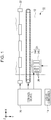
- Fig. 1 is a view illustrating a configuration of a liquid discharging apparatus 10 according to a first embodiment of the invention.
- the liquid discharging apparatus 10 of the first embodiment is an ink jet printing apparatus that discharges an ink, which is an example of a liquid, onto a medium 12.
- the medium 12 is typical printing paper, any printing target such as a resin film and cloth can be used as the medium 12.
- a liquid container 14 storing an ink is fixed to the liquid discharging apparatus 10.
- a cartridge that is attachable/detachable to/from the liquid discharging apparatus 10 a bag-like ink pack formed of a flexible film, or an ink tank that can be refilled with an ink is used as the liquid container 14.
- a plurality of types of inks having different colors are stored in the liquid container 14.
- the liquid discharging apparatus 10 includes a control device 20, a transporting mechanism 22, a moving mechanism 24, and a plurality of liquid discharging heads 26.
- the control device 20 includes, for example, a processing circuit, such as a central processing unit (CPU) and a field programmable gate array (FPGA), and a memory circuit, such as a semiconductor memory, and comprehensively controls each element of the liquid discharging apparatus 10.
- the transporting mechanism 22 transports the medium 12 in a Y-direction under the control of the control device 20.
- the moving mechanism 24 causes the plurality of liquid discharging heads 26 to reciprocate in an X-direction under the control of the control device 20.
- the X-direction is a direction intersecting (typically orthogonal to) the Y-direction in which the medium 12 is transported.
- the moving mechanism 24 includes a carriage 242 on which the plurality of liquid discharging heads 26 are mounted and an endless belt 244 to which the carriage 242 is fixed. It is also possible to mount the liquid container 14 on the carriage 242 with the liquid discharging heads 26.
- Each of the plurality of liquid discharging heads 26 discharges an ink, which is supplied from the liquid container 14, onto the medium 12 from a plurality of nozzles (discharge holes) N under the control of the control device 20.
- a desired image is formed on an outer surface of the medium 12 by each of the liquid discharging heads 26 discharging an ink onto the medium 12 as the transportation of the medium 12 by the transporting mechanism 22 and the repeated reciprocation of the carriage 242 are performed at the same time.
- a direction perpendicular to an XY-plane for example, a plane parallel to the outer surface of the medium 12
- a direction (typical vertical direction), in which an ink is discharged by each of the liquid discharging heads 26, corresponds to the Z-direction.
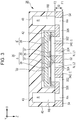
- Fig. 2 is an exploded perspective view of any one of the liquid discharging heads 26, and Fig. 3 is a sectional view taken along line III-III of Fig. 2 .
- the liquid discharging head 26 includes the plurality of nozzles N arranged in the Y-direction.
- the plurality of nozzles N of the first embodiment are classified into a first line L1 and a second line L2.
- the liquid discharging head 26 has a structure in which elements related to the plurality of nozzles N in the first line L1 and elements related to the plurality of nozzles N in the second line L2 are disposed so as to be substantially linearly symmetric to each other.
- the liquid discharging head 26 includes a flow path substrate 32.
- the flow path substrate 32 is a plate-like member including an outer surface F1 and an outer surface F2.
- the outer surface F1 is an outer surface (outer surface on a medium 12 side) on a positive side of the Z-direction
- the outer surface F2 is an outer surface on a side (negative side of the Z-direction) opposite to the outer surface F1.
- a pressure generating unit 35 and a case member 40 are provided on the outer surface F2 of the flow path substrate 32, and a nozzle plate 52 and compliance substrates 54 are provided on the outer surface F1.
- Each element of the liquid discharging head 26 is a substantially plate-like member which is long in the Y-direction just as the flow path substrate 32.
- the elements are bonded to each other using, for example, an adhesive. It is also possible to perceive a direction, in which the flow path substrate 32 and a pressure chamber substrate 34 are stacked, as the Z-direction.
- the pressure generating unit 35 is an element that causes a pressure change for discharging inks from the nozzles N.
- the pressure generating unit 35 of the embodiment is configured by a first substrate A including the pressure chamber substrate 34 and the piezoelectric device 39, a second substrate B including a wiring connection substrate (protection substrate) 38, and a drive IC 62 being bonded to each other.
- the piezoelectric device 39 is formed of pressure chambers C (to be described later) formed in the pressure chamber substrate 34, piezoelectric elements 37, and a diaphragm 36 disposed between the pressure chambers C and the piezoelectric elements 37, and is an element that causes a pressure change in the pressure chambers C by vibration. Details of the pressure generating unit 35 and the piezoelectric device 39 will be described later.
- the nozzle plate 52 is a plate-like member in which the plurality of nozzles N are formed, and is provided on the outer surface F1 of the flow path substrate 32 using, for example, an adhesive. Each of the nozzles N is a through-hole through which an ink passes.
- the nozzle plate 52 of the first embodiment is manufactured by processing a single crystal silicon (Si) base (silicon substrate) using a semiconductor manufacturing technique. However, any known material or any known manufacturing method can be adopted in manufacturing the nozzle plate 52.
- the flow path substrate 32 is a plate-like member for forming a flow path of an ink. As illustrated in Figs. 2 and 3 , a space RA, a plurality of supply flow paths 322, and a plurality of communication flow paths 324 are formed for each of the first line L1 and the second line L2 in the flow path substrate 32.
- the spaces RA are long openings which run in the Y-direction in plan view (that is, seen from the Z-direction), and the supply flow path 322 and the communication flow path 324 are through-holes formed for each of the nozzles N.
- the plurality of supply flow paths 322 are arranged in the Y-direction, and the plurality of communication flow paths 324 are also arranged in the Y-direction.
- intermediate flow paths 326 which reach the plurality of supply flow paths 322 are formed in the outer surface F1 of the flow path substrate 32.
- Each of the intermediate flow paths 326 is a flow path connecting the space RA and the plurality of supply flow paths 322 together.
- the communication flow paths 324 communicate with the nozzles N.
- the wiring connection substrate 38 of Figs. 2 and 3 is a plate-like member for protecting the plurality of piezoelectric elements 37, and is provided on an outer surface (outer surface on a side opposite to the pressure chambers C) of the diaphragm 36.
- the wiring connection substrate 38 can be formed by processing a single crystal silicon (Si) base (silicon substrate) using a semiconductor manufacturing technique as in the case of the flow path substrate 32 and the pressure chamber substrate 34. As illustrated in Figs.
- the drive IC 62 is provided on an outer surface of the wiring connection substrate 38 (hereinafter, referred to as a "mount surface") on a side opposite to the outer surface (hereinafter, referred to as a "bonded surface”) on a diaphragm 36 side.
- the drive IC 62 is a substantially rectangular IC chip on which a drive circuit that drives each of the piezoelectric elements 37 by generating and supplying a drive signal under the control of the control device 20 is mounted.
- wiring 384 connected to an output terminal for a drive signal (drive voltage) of the drive IC 62 is formed for each of the piezoelectric elements 37.
- each of wiring pieces 385 connected to an output terminal for a base voltage (base voltage of a drive signal of each of the piezoelectric elements 37) of the drive IC 62 is consecutively formed on the mount surface of the wiring connection substrate 38 along the disposition of the piezoelectric elements 37 in the Y-direction.
- the case member 40 illustrated in Figs. 2 and 3 is a case for storing an ink to be supplied to the plurality of pressure chambers C (furthermore, the plurality of nozzles N).
- An outer surface of the case member 40 on the positive side of the Z-direction is fixed to the outer surface F2 of the flow path substrate 32 with, for example, an adhesive.
- a grooved recessed portion 42 extending in the Y-direction is formed in the outer surface of the case member 40 on the positive side of the Z-direction.
- the wiring connection substrate 38 and the drive IC 62 are accommodated inside the recessed portion 42.
- the case member 40 is formed of a material different from materials of the flow path substrate 32 and the pressure chamber substrate 34.
- the case member 40 It is possible to manufacture the case member 40 with, for example, a resin material by injection molding. However, any known material or any known manufacturing method can be adopted in manufacturing the case member 40. For example, a synthetic fiber or a resin material is suitable as a material of the case member 40.
- a space RB is formed for each of the first line L1 and the second line L2 in the case member 40.
- the spaces RB of the case member 40 and the spaces RA of the flow path substrate 32 communicate with each other.
- a space configured of the space RA and the space RB functions as a liquid storing chamber (reservoir) R storing an ink to be supplied to the plurality of pressure chambers C.
- the liquid storing chamber R is a common liquid chamber that reaches the plurality of nozzles N.
- An inlet 43 for causing an ink to be supplied from the liquid container 14 to flow into the liquid storing chamber R is formed for each of the first line L1 and the second line L2 in the outer surface of the case member 40 on a side opposite to the flow path substrate 32.
- An ink supplied from the liquid container 14 to the inlet 43 is stored in the space RB and the space RA of the liquid storing chamber R.
- the ink stored in the liquid storing chamber R is divided into the plurality of supply flow paths 322 from the intermediate flow paths 326 so as to be supplied to and so as to fill each of the pressure chambers C in parallel.
- the compliance substrates 54 are provided on the outer surface F1.
- the compliance substrates 54 are flexible films that absorb a pressure change of an ink in the liquid storing chambers R.
- the compliance substrates 54 are provided on the outer surface F1 of the flow path substrate 32 so as to close the spaces RA of the flow path substrate 32, the intermediate flow paths 326, and the plurality of supply flow paths 322, and configure wall surfaces (specifically, bottom surfaces) of the liquid storing chamber R.
- the pressure generating unit 35 illustrated in Fig. 3 is configured by stacking the first substrate A, the second substrate B, and the drive IC 62.
- the first substrate A is a substrate that includes the pressure chamber substrate 34, the diaphragm 36, and the plurality of piezoelectric elements 37
- the second substrate B is a substrate that includes the wiring connection substrate 38.
- the pressure chamber substrate 34 is a plate-like member, in which a plurality of openings 342 configuring the pressure chambers C are formed for each of the first line L1 and the second line L2, and is provided on the outer surface F2 of the flow path substrate 32 using, for example, an adhesive.
- the plurality of openings 342 are arranged in the Y-direction.
- Each of the openings 342 is a through-hole, which is formed for each of the nozzles N and runs in the X-direction in plan view.
- the flow path substrate 32 and the pressure chamber substrate 34 are manufactured by processing single crystal silicon (Si) substrates (silicon substrates) using a semiconductor manufacturing technique as in the case of the nozzle plate 52 described above. However, any known material and any known method can be adopted in manufacturing the flow path substrate 32 and the pressure chamber substrate 34.
- the piezoelectric device 39 is provided on an outer surface of the pressure chamber substrate 34 on a side opposite to the flow path substrate 32.
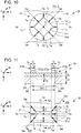
- Fig. 4 is a sectional view and a plan view of the enlarged piezoelectric device 39.
- the sectional view (view on the upper side of Fig. 4 ) of Fig. 4 is a view obtained by cutting the piezoelectric device 39 with an XZ-plane
- the plan view (view on the lower side of Fig. 4 ) of Fig. 4 is a view in which the piezoelectric device 39 is seen from the Z-direction.
- Fig. 5 is a sectional view of the piezoelectric device 39 illustrated in Fig. 4 taken along line V-V.
- a W direction of Figs. 4 and 5 is a direction where an angle of 45 degrees is formed counterclockwise from the X-direction, and is a direction along an axis Gw to be described later.
- the piezoelectric device 39 is formed of the pressure chambers C, the piezoelectric elements 37, and the diaphragm 36, and causes a pressure change in each of the pressure chambers C by the piezoelectric elements 37 vibrating the diaphragm 36.
- the shape of the inner periphery 345 of the pressure chamber C of Fig. 4 is a square. Specifically, the shape of the inner periphery 345 of the pressure chamber C is a square in plan view.
- the shape of the inner periphery 345 of the pressure chamber C is the shape of the inner periphery 345 of a side wall 344 of the pressure chamber C in plan view seen from the Z-direction, and defines a vibration region P of the diaphragm 36.
- the vibration region P of the diaphragm 36 is a region of the diaphragm 36, which overlaps the pressure chamber C in plan view, and is a region that configures a wall surface (top surface) of the pressure chamber C.
- the piezoelectric element 37 of Fig. 4 is a square-annular element of which the shape of an inner edge 37A is a square and the shape of an outer edge 37B is a square larger than the square of the inner edge 37A in plan view (seen from the Z-direction). Specifically, the piezoelectric element 37 is disposed on the diaphragm 36 so as to overlap the inner periphery 345 of the pressure chamber C without overlapping a center O of the pressure chamber C in plan view.
- the piezoelectric element has the inner edge 37A on a center O side of the pressure chamber C and has the outer edge 37B on a side wall 344 side of the pressure chamber C with the inner periphery 345 of the pressure chamber C being sandwiched between the outer edge and the inner edge.
- a case where the entire perimeter of the piezoelectric element 37 is annularly formed so as to overlap the entire perimeter of the inner periphery 345 of the pressure chamber C in plan view is given as an example in Fig. 4 .
- the piezoelectric elements 37 may have a configuration of overlapping some parts of the inner peripheries 345 instead of the entire perimeters of the inner peripheries 345 of the pressure chambers C.
- the outer surface F2 of the flow path substrate 32 and the diaphragm 36 face each other at an interval inside each of the openings 342.
- a space positioned inside each of the openings 342 between the outer surface F2 of the flow path substrate 32 and the diaphragm 36 functions as each of the pressure chambers C for applying a pressure to an ink which has filled the space.
- the pressure chamber C is separately formed for each of the nozzles N.
- the plurality of pressure chambers C (openings 342) are arranged in the Y-direction for each of the first line L1 and the second line L2. Any one of the pressure chambers C communicates with the space RA via the supply flow path 322 and the intermediate flow path 326, and communicates with the nozzle N via the communication flow path 324.
- the plurality of piezoelectric elements 37 corresponding to the different nozzles N are provided for each of the first line L1 and the second line L2 as illustrated in Figs. 2 to 5 .
- the piezoelectric elements 37 are pressure generating elements that deform due to supply of a drive signal and generate pressures in the pressure chambers C.
- Each of the plurality of piezoelectric elements 37 is arranged in the Y-direction so as to correspond to each of the pressure chambers C.
- Each of the piezoelectric elements 37 is a stacked body of which a piezoelectric layer is sandwiched between a first electrode and a second electrode, which face each other.
- a piezoelectric strain occurs in the piezoelectric layer sandwiched between the first electrode and the second electrode and thus the piezoelectric layer is displaced. Therefore, each of the piezoelectric elements 37 is a portion in which the first electrode, the second electrode, and the piezoelectric layer overlap each other.
- a pressure in each of the pressure chambers C changes by the diaphragm 36 vibrating in tandem with a piezoelectric strain of the piezoelectric layer 373.
- An adhesive layer for ensuring adhesion may be provided between the piezoelectric elements 37 and the diaphragm 36. That is, it is not necessary for the piezoelectric elements 37 to be directly provided on the outer surface of the diaphragm 36, and the piezoelectric elements may be provided on the outer surface of the diaphragm 36 via the adhesive layer.
- Zirconium, a zirconium oxide, titanium, a titanium oxide, and a silicon oxide can be used for the adhesive layer.
- the diaphragm 36 is a plate-like member that can elastically vibrate.
- the diaphragm 36 of the embodiment is configured of an anisotropic single crystal silicon base of which a Young's modulus varies according to a direction in a crystal plane, and the outer surface of the diaphragm 36 is configured of a crystal plane of the single crystal silicon base.
- a crystal of the single crystal silicon base is not limited to being as the outer surface of the diaphragm 36, and may be included at least in the diaphragm 36.
- the crystal of the single crystal silicon base may be included in the stacked materials.
- the diaphragm 36 is stacked and bonded to the side walls 344 (pressure chamber substrate 34) of the pressure chambers C and configures a wall surface (specifically, a top surface) intersecting the side walls 344 of the pressure chambers C.
- regions (regions configuring the top surfaces of the pressure chambers C) of the diaphragm 36, which overlap the pressure chambers C in plan view, are the vibration regions P that vibrate due to the piezoelectric elements 37.
- Each of the piezoelectric elements 37 of the embodiment includes an inner peripheral portion 372a that overlaps the pressure chamber C in plan view (seen from the Z-direction) and an outer peripheral portion 372b that overlaps the side wall 344 of the pressure chamber C in plan view.
- the inner peripheral portions 372a are portions that are displaced in the Z-direction in tandem with piezoelectric strains of piezoelectric layers 373.
- the outer peripheral portions 372b are portions (portions that are not displaced in the Z-direction) of which displacement in the Z-direction is restrained by the side walls 344 of the pressure chambers C.
- Each of the vibration regions P of the embodiment is a square having the same size as the pressure chamber C in plan view, and has an axis Gx that passes through the center O in the X-direction and an axis Gy that passes through the center O in the Y-direction. Since each of the vibration regions P of the embodiment is a square, the length of the vibration region P in a direction of the axis Gx is equal to the length of the vibration region in a direction of the axis Gy.
- each of the vibration regions P has a shape of which the length in the direction of the axis Gy and the length in direction of the axis Gx are different from each other, a short axis of the smallest rectangle which includes one of the vibration regions P will be set as the axis Gy of the vibration region P and a long axis of the smallest rectangle that includes the vibration region P will be set as the axis Gx of the vibration region P.
- Fig. 6 is a graph showing an example of anisotropy of a Young's modulus in a (100) plane of a single crystal silicon base of which the crystal plane is the (100) plane (crystal plane orientation perpendicular to the crystal plane is [100]).
- Fig. 6 is expressed in polar coordinates, and the Young's modulus becomes higher as a distance from the center becomes longer.
- the Young's modulus in the (100) plane of the single crystal silicon base of which the crystal plane is the (100) plane has substantially square anisotropy.
- a Young's modulus is minimum in four crystal orientations [010], [001], [0-10], and [00-1].
- a Young's modulus is maximum, for example, at orientations Dn having an angle of 45 degrees counterclockwise from the orientations Dm. Therefore, even if the direction of the axis Gx of the vibration region P is aligned with the orientation Dm (for example, the crystal orientation [010]), for example, in order to make a Young's modulus lower to make the diaphragm 36 likely to be displaced, the diaphragm in the orientation Dn in which the Young's modulus is maximum is unlikely to be displaced in the Z-direction only by doing so. For this reason, the displacement of the diaphragm 36 in the Z-direction as a whole is inhibited and thus the displacement of the entire diaphragm 36 cannot be sufficiently improved.
- the orientation Dm for example, the crystal orientation [010]
- the widths of the piezoelectric elements 37 in the first direction is larger than the widths of the piezoelectric elements 37 in the second direction.
- an area where the piezoelectric elements 37 are driven in a direction where a Young's modulus is high which is a direction where the displacement H of the diaphragm 36 is likely to be obstructed, can be made wider than an area where the piezoelectric elements are driven in a direction where a Young's modulus is low.
- the shape of the pressure chamber C (the shape of the vibration region P) is a square as illustrated in Fig. 4
- the shape of the inner edge (inner periphery) 37A of the piezoelectric element 37 is a square that is smaller than the pressure chamber C
- the shape of the outer edge (outer periphery) 37B is a square that is larger than the pressure chamber C. Accordingly, the width of the piezoelectric element 37 in a direction where a Young's modulus is high can be made larger than the width of the piezoelectric element 37 in a direction where a Young's modulus is low.
- a configuration of such a piezoelectric element 37 of Figs. 4 and 5 will be described more specifically.
- a direction along a crystal orientation [011] in which a Young's modulus is maximum will be set as the first direction
- a direction along the crystal orientation [010] in which a Young's modulus is minimum will be set as the second direction.
- a direction (axis along the W direction) where an angle of 45 degrees is formed counterclockwise from the axis Gx is set as Gw
- the axis Gx of the vibration region P runs in the second direction
- the axis Gw run in the first direction.
- the shape of the inner edge 37A of the piezoelectric element 37 is a square smaller than the pressure chamber C and the shape of the outer edge 37B is a square larger than the pressure chamber C. Therefore, a width Tw (a upper right width or a lower left width in the plan view of Fig. 4 ) of the piezoelectric element 37 in the direction (first direction) of the axis Gw where a Young's modulus is maximum is larger than a width Tx (a left width or a right width in the plan view of Fig. 4 ) of the piezoelectric element 37 in the direction (second direction) of the axis Gx where a Young's modulus is minimum.
- the width Tw along the axis Gw is equal to a width Tw' along the axis Gw'
- the width Tx along the axis Gx is equal to a width Ty along the axis Gy.
- the width Tw and the width Tw' are larger than the width Tx and the width Ty.
- an area where the piezoelectric elements 37 are driven in a direction where a Young's modulus is high which is a direction where the displacement of the diaphragm 36 is likely to be obstructed, can be made wider than an area where the piezoelectric elements are driven in a direction where a Young's modulus is low. Accordingly, since a deflection amount can be increased in an in-plane direction where a Young's modulus is high, the same amount as a deflection amount in an in-plane direction where a Young's modulus is low can be applied. Thus, an even strain can occur in the entire diaphragm 36. Therefore, as shown with a one dot chain line of Fig.
- the displacement H greater than displacement H' which occurs in a case where the width of the piezoelectric element 37 in the direction along the axis Gw is made the same as the width Tx in the direction along the axis Gx, can occur.
- the entire diaphragm 36 is likely to be displaced, and thus the displacement efficiency of the diaphragm 36 can be improved.
- the configuration of the embodiment is applicable also to a case where a (010) plane or a (001) plane, which is a crystal plane equivalent to the crystal plane (100), is the outer surface (top surface) of the diaphragm 36 since single crystal silicon has a cubic crystal system. Even when the crystal plane is the (010) plane or the (001) plane, the Young's modulus is in a shape shown in Fig. 6 .
- crystal orientations [-100], [-101], and [001] are applied by replacing the three reference crystal orientations [010], [011], and [001] in Fig. 6 , respectively.
- crystal orientations [010], [-110], and [-100] are applied by replacing the crystal orientations [010], [011], and [001] in Fig. 6 , respectively.
- all of the crystal planes (100), (010), and (001) are equivalent to each other, and a plane group of the crystal planes can be altogether referred to as a crystal plane ⁇ 100 ⁇ .
- crystal orientation [010] in the (100) plane, the crystal orientation [-100] in the (010) plane, and the crystal orientation [010] in the (001) plane are equal to each other, a direction group of the crystal orientation [010] and equivalents thereof can be altogether referred to as a crystal orientation ⁇ 010>.
- a direction group of the crystal orientation [011] and equivalents thereof can be altogether referred to as a crystal orientation ⁇ 011>
- a direction group of the crystal orientation [010] and equivalents thereof can be altogether referred to as a crystal orientation ⁇ 001>.
- the diaphragm 36 may be formed of a single crystal silicon base of which the crystal plane is a (110) plane (crystal plane orientation perpendicular to the crystal plane is [110]) as shown in Fig. 7.
- Fig. 7 is a graph showing an example of anisotropy of a Young's modulus in the (110) plane of the single crystal silicon base of which the crystal plane is the (110) plane.
- Fig. 7 is expressed in polar coordinates, and a Young's modulus becomes higher as a distance from the center becomes longer.
- the Young's modulus in the (110) plane of the single crystal silicon base has substantially rectangular anisotropy.
- a Young's modulus in the (110) plane, for example, a Young's modulus is minimum in the crystal orientation [001], and for example, a Young's modulus is maximum in a crystal orientation [1-11] of 55 degrees counterclockwise from the crystal orientation [001].
- the width of the piezoelectric element 37 in the first direction is larger than the width of the piezoelectric element 37 in the second direction in a case where a Young's modulus in the first direction in the crystal plane is higher than a Young's modulus in the second direction in the crystal plane.
- an area where the piezoelectric elements 37 are driven in a direction where a Young's modulus is high which is a direction where the displacement of the diaphragm 36 is likely to be obstructed, can be made wider than an area where the piezoelectric elements are driven in a direction where a Young's modulus is low.
- the first direction may not necessarily be a crystal orientation in which a Young's modulus is maximum
- the second direction may not necessarily be a crystal orientation in which a Young's modulus is minimum.
- a Young's modulus is not maximum but is higher than a minimum value.
- an area where the piezoelectric elements 37 are driven in a direction where a Young's modulus is high which is a direction where the displacement of the diaphragm 36 is likely to be obstructed, can be made wider than an area where the piezoelectric elements are driven in a direction where a Young's modulus is low.
- the axis Gw of the vibration region P illustrated in Fig. 4 runs in the first direction, and the axis Gx runs in the second direction. Therefore, when the direction of the axis Gx of the vibration region P illustrated in Fig. 4 is made so as to run in the orientation Dm (for example, the crystal orientation [001]), the axis Gw runs in the orientation Dn', in which a Young's modulus is higher than a Young's modulus in the orientation Dm, since the axis Gw has an angle of 45 degrees with respect to the axis Gx.
- the piezoelectric elements 37 each having the shape illustrated in Fig.
- the width Tw of the piezoelectric element 37 in the direction of the axis Gw where a Young's modulus is high can be made larger than the width Tx of the piezoelectric element 37 in the direction of the axis Gx where a Young's modulus is low.
- a deflection amount in the in-plane direction where a Young's modulus is high can be increased also in a case where the diaphragm 36 of Fig. 4 is configured of the single crystal silicon base of which the crystal plane is the (110) plane, the same amount as a deflection amount in the in-plane direction where a Young's modulus is low can be applied. Consequently, since an even strain can occur in the entire diaphragm 36, the entire diaphragm 36 is likely to be displaced and thus the displacement efficiency of the diaphragm 36 can be improved.
- the configuration is applicable also to a case where a (011) plane or a (101) plane, which is a crystal plane equivalent to the crystal plane (110), is the outer surface (top surface) of the diaphragm 36 since single crystal silicon has a cubic crystal system. Even when the crystal plane is the (011) plane or the (101) plane, the Young's modulus is in a shape shown in Fig. 7 .
- crystal orientations [1-11], [1-12], [100], [21-1], [11-1], [01-1], and [-11-1] are applied by replacing the seven reference crystal orientations [-111], [-112], [001], [1-12], [1-11], [1-10], and [1-1-1] in Fig. 7 , respectively.
- crystal orientations [11-1], [12-1], [010], [-121], [-1-11], [-101], and [-1-11] are applied by replacing the seven reference crystal orientations [-111], [-112], [001], [1-12], [1-11], [1-10], and [1-1-1] in Fig.
- crystal planes (110), (011), and (101) are equivalent to each other, and a plane group of the crystal planes can be altogether referred to as a crystal plane ⁇ 110 ⁇ .
- a direction group of the crystal orientations can be altogether referred to as a crystal orientation ⁇ 111>.
- a direction group of the crystal orientation [001] and equivalents thereof can be altogether referred to as ⁇ 001>.
- each of the shape of the pressure chamber C, the shape of the inner edge 37A of the piezoelectric element 37, and the shape of the outer edge 37B of the piezoelectric element 37 is a square is given as an example in the embodiment, the shapes are not limited thereto.
- the shape of the pressure chamber C is a shape when the inner periphery 345 of the pressure chamber C is in plan view (seen from the Z-direction), and is the same as the shape of the vibration region P.
- the shape of the inner edge 37A of the piezoelectric element 37 is a shape when the inner edge 37A of the piezoelectric element 37 is in plan view (seen from the Z-direction), and the shape of the outer edge 37B of the piezoelectric element 37 is a shape when the outer edge 37B of the piezoelectric element 37 is in plan view (seen from the Z-direction).
- Each of the shape of the pressure chamber C (the shape of the vibration region P), the shape of the inner edge 37A of the piezoelectric element 37, and the shape of the outer edge 37B of the piezoelectric element 37 may be other than a square such as a polygon or a circle.
- the polygon also includes a rounded polygon such as a rounded square and a rounded rectangle.
- the circle also includes a substantially circle (a semicircle and a sector).
- the shape of the pressure chamber C (the shape of the vibration region P), the shape of the inner edge 37A of the piezoelectric element 37, and the shape of the outer edge 37B of the piezoelectric element 37 may be different from each other. Even when the pressure chamber C and the piezoelectric element 37 are other than squares, the shape of the inner edge 37A of the piezoelectric element 37 and the shape of the outer edge 37B of the piezoelectric element 37 are determined in accordance with the shape of the pressure chamber C such that the width of the piezoelectric element 37 in the first direction is larger than the width of the piezoelectric element 37 in the second direction in a case where a Young's modulus in the first direction is higher than a Young's modulus in the second direction.
- a first modification example of the first embodiment illustrated in Fig. 8 is a case where the shape of the pressure chamber C (the shape of the vibration region P) is a perfect circle.
- the shape of the inner edge 37A of the piezoelectric element 37 is a diamond, which is smaller than the pressure chamber C and is obtained by rotating a square 45 degrees
- the shape of the outer edge 37B of the piezoelectric element 37 is a perfect circle larger than the pressure chamber C.
- a second modification example of the first embodiment illustrated in Fig. 9 is a case where the shape of the pressure chamber C (the shape of the vibration region P) is a diamond, which is obtained by rotating the square of Fig. 4 45 degrees.
- the shape of the inner edge 37A of the piezoelectric element 37 is an octagon, which is smaller than the pressure chamber C, is projected in the directions of the axis Gx and the axis Gy, and is recessed in the directions of the axes Gw and Gw', and the shape of the outer edge 37B of the piezoelectric element 37 is a diamond larger than the pressure chamber C.
- the width of the piezoelectric element 37 in a direction where a Young's modulus is high can be made larger than the width of the piezoelectric element 37 in a direction where a Young's modulus is low.
- the direction of the axis Gw of the vibration region P is set as a direction where a Young's modulus is minimum
- the direction of the axis Gw of the vibration region P is a direction where a Young's modulus is maximum, as in Fig. 4 .
- the width Tw an upper right width and a lower left width in the plan view of Figs. 8 and 9
- the vibration regions P and the piezoelectric elements 37 of Figs. 8 and 9 also have the length in the direction of the axis Gx which is the same as the length in the direction of the axis Gy, are linearly symmetric with respect to the axis Gx, and are also linearly symmetric with respect to the axis Gy. Therefore, in the vibration region P, a Young's modulus is maximum also in the direction of the axis Gw' orthogonal to the axis Gw and a Young's modulus is minimum also in the direction of the axis Gy orthogonal to the axis Gx.
- the width of the piezoelectric element 37 in any of the directions (first direction) of the axis Gw and the axis Gw' where a Young's modulus is maximum is larger than the width of the piezoelectric element 37 in any of the directions (second direction) of the axis Gx and the axis Gy where a Young's modulus is minimum.
- the first direction may not necessarily be a crystal orientation in which a Young's modulus is maximum
- the second direction may not necessarily be a crystal orientation in which a Young's modulus is minimum.
- an area where the piezoelectric elements 37 are driven in a direction where a Young's modulus is high which is a direction where the displacement of the diaphragm 36 is likely to be obstructed, can be made wider than an area where the piezoelectric elements are driven in a direction where a Young's modulus is low, also in Figs. 8 and 9 . Accordingly, since a deflection amount in an in-plane direction where a Young's modulus is high can be increased, the same amount as a deflection amount in the in-plane direction where a Young's modulus is low can be applied. Consequently, since an even strain can occur in the entire diaphragm 36, the displacement efficiency of the diaphragm 36 can be improved.
- a width T of the piezoelectric element 37 can be changed.
- the width T of the piezoelectric element 37 is a width between the inner edge 37A and the outer edge 37B, and includes the widths Tx, Ty, Tw, and Tw' in each direction.
- the width T of the piezoelectric element 37 can be divided into a width Ta of a portion that overlaps the pressure chamber C in plan view and a width Tb of a portion that overlaps the side wall 344 of the pressure chamber C in plan view.
- the width Ta of the piezoelectric element 37 is the width of the inner peripheral portion 372a
- the width Tb is the width of the outer peripheral portion 372b.
- both of the width Ta and the width Tb of the piezoelectric element 37 may be changed according to the shapes of the inner edge 37A and the outer edge 37B of the piezoelectric element 37, or any one of the width Ta and the width Tb may be changed.
- the width Ta can be changed by changing the shape of the inner edge 37A of the piezoelectric element 37
- the width Tb can be changed by changing the shape of the outer edge 37B of the piezoelectric element 37.
- the width Tb of the piezoelectric element 37 is almost constant. According to the shape of the inner edge 37A of the piezoelectric element 37, the width Ta of the portion of the piezoelectric element 37 that overlaps the pressure chamber C in plan view, becomes larger in a direction where a Young's modulus is high in a crystal plane than in a direction where a Young's modulus is low in the crystal plane. However, the width Tb of the piezoelectric element 37 may not be constant.
- the width Tb of the portion of the piezoelectric element 37 that overlaps the side wall 344 of the pressure chamber C in plan view can become larger in a direction where a Young's modulus is high in a crystal plane than in a direction where a Young's modulus is low in the crystal plane.
- the shape of the inner edge 37A of the piezoelectric element 37 is a diamond smaller than the pressure chamber C
- the outer edge 37B is a perfect circle larger than the pressure chamber C in a case where the shape of the pressure chamber C is the same diamond of Fig. 8 .
- the width Ta of the piezoelectric element 37 is almost constant. According to the shape of the outer edge 37B of the piezoelectric element 37, the width Tb of the portion of the piezoelectric element 37 that overlaps the side wall 344 of the pressure chamber C in plan view becomes larger in a direction where a Young's modulus is high in a crystal plane than in a direction where a Young's modulus is low in the crystal plane. However, the width Ta of the piezoelectric element 37 may not be constant.
- the direction of the axis Gx of the vibration region P lies in the orientation Dn in which a Young's modulus is maximum or the orientation Dn' near to the orientation Dn
- the direction is not limited thereto.
- the direction of the axis Gy of the vibration region P may be aligned with the orientation Dn in which a Young's modulus is maximum or an orientation in which a Young's modulus is higher than a Young's modulus in the direction of the axis Gw. Even in this way, the same effect as the embodiment can be obtained by forming the piezoelectric elements 37 so as to have the same shapes as in Fig. 4 and Figs. 8 to 10 .
- a second embodiment of the invention will be described.
- elements, of which operation and functions are the same as in the first embodiment will be assigned with the same reference signs used in describing the first embodiment and detailed description of each of the elements will be omitted as appropriate.
- the shape of the pressure chamber C (the shape of the vibration region P) of which the length in the direction of the axis Gx is the same as the length in the direction of the axis Gy is given as an example.
- the shape of the pressure chamber C (the shape of the vibration region P) of which the length in the direction of the axis Gx is different from the length in the direction of the axis Gy will be given as an example.
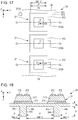
- Fig. 11 is a sectional view and a plan view of the enlarged piezoelectric device 39 of the second embodiment.
- the sectional view (view on the upper side of Fig. 11 ) of Fig. 11 is a view obtained by cutting the piezoelectric device 39 with the XZ-plane
- the plan view (view on the lower side of Fig. 11 ) of Fig. 11 is a view in which the piezoelectric device 39 is seen from the Z-direction.
- Fig. 12 is a sectional view of the piezoelectric device 39 illustrated in Fig. 11 taken along line XII-XII
- Fig. 13 is a sectional view of the piezoelectric device 39 illustrated in Fig. 11 taken along line XIII-XIII.
- the shape of the pressure chamber C (the shape of the vibration region P) is, in plan view, a rectangle formed of a long axis, which runs in the X-direction, and a short axis, which is shorter than the long axis and runs in the Y-direction.
- the long axis, which runs in the X-direction will be set as the axis Gx
- the short axis, which runs in the Y-direction will be set as the axis Gy.
- the shapes of the vibration regions P may be shapes other than a rectangle.
- each of the vibration regions P has a shape other than a rectangle
- a short axis of the smallest rectangle that includes one of the vibration regions P is the axis Gy of the vibration region P
- a long axis of the smallest rectangle that includes the vibration region P is the axis Gx of the vibration region P.
- the displacement H in the Z-direction occurs in middle portions of the vibration regions P of the diaphragm 36 due to piezoelectric strains of the piezoelectric elements 37 as illustrated with dotted lines of Figs. 11 to 13 .
- the portions close to the side walls 344 in the Y-direction (direction of the axis Gy), which are illustrated in the sectional view of Fig. 12
- the displacement of the entire diaphragm 36 is likely to be obstructed in the direction of the long axis Gx by the displacement in the direction of the short axis Gy, and if a deflection amount in the direction of the short axis Gy can be increased, an even strain can occur in the entire diaphragm 36.
- the width Ty of the piezoelectric element 37 in the direction of the short axis Gy of the smallest rectangle that includes the vibration region P is larger than the width Tx of the pressure chamber C in the direction of the long axis Gx of the rectangle. According to this configuration, an area where the piezoelectric elements 37 are driven in the direction of the short axis Gy where displacement of the diaphragm 36 is likely to be obstructed can be made wider than an area where the piezoelectric elements are driven in the direction of the long axis Gx.
- the shape of the pressure chamber C (the shape of the vibration region P) is a rectangle as illustrated in Fig. 11
- the shape of the inner edge 37A of the piezoelectric element 37 is a rectangle smaller than the pressure chamber C and the shape of the outer edge 37B is a rectangle larger than the pressure chamber C.
- the width Ty in the direction of the axis Gy is made larger than the width Tx in the direction of the axis Gx.
- an area where the piezoelectric elements 37 are driven in the direction of the short axis Gy where the displacement H of the diaphragm 36 is likely to be obstructed can be made wider than an area where the piezoelectric elements are driven in the direction of the long axis Gx. Accordingly, since a deflection amount can be increased in the direction of the short axis Gy, the same amount as a deflection amount in the direction of the long axis Gx can be applied. Consequently, since a deflection amount of the diaphragm 36 in the in-plane direction can be increased, an even strain can occur in the entire diaphragm 36. Therefore, the entire diaphragm 36 is likely to be displaced, and thus the displacement efficiency of the diaphragm 36 can be improved.
- the width of the piezoelectric element 37 in the first direction is larger than the width of the piezoelectric element 37 in the second direction, as in the first embodiment.
- the diaphragm 36 is configured of the single crystal silicon base having the crystal plane of Fig. 6 or 7 , and the orientation Dn in which a Young's modulus is high or a direction along the orientation Dn' can be set as the first direction and a direction along the orientation Dm in which a Young's modulus is minimum can be set as the second direction.
- the axis Gw of the vibration region P runs in the first direction and the axis Gy runs in the second direction.
- the width Tw an upper right width or a lower left width in the plan view of Fig. 11
- the width Ty an upper width or a lower width in the plan view of Fig.
- the width Tw' (an upper left width and a lower right width in the plan view of Fig. 11 ) in the direction of the axis Gw' is larger than the width Ty (an upper width or a lower width in the plan view of Fig. 11 ) of the piezoelectric element 37 in the direction of the axis Gy where a Young's modulus is minimum since a Young's modulus is also higher in the direction of the axis Gw' than in the direction of the axis Gy.
- an area where the piezoelectric elements are driven in a direction where a Young's modulus is high which is a direction where the displacement of the diaphragm 36 is likely to be obstructed, can be made wider.
- a deflection amount of the diaphragm 36 in the in-plane direction can be increased also in a direction where a Young's modulus is high. Therefore, an effect of improving the displacement efficiency of the diaphragm 36 can be enhanced in the vibration region P of which the length in the direction of the axis Gx and the length in the direction of the axis Gy are different from each other.
- the width Tw of the piezoelectric element 37 in a direction (first direction) along the axis Gw where a Young's modulus is high is set as a first width and the width Ty in a direction (second direction) along the axis Gy where a Young's modulus is low is set as a second width
- the first width and the second width are larger than the width Tx of the piezoelectric element 37 in the direction of the long axis Gx.
- the shape (the shape of the vibration region P) of the pressure chamber C, the shape of the inner edge 37A of the piezoelectric element 37, and the shape of the outer edge 37B of the piezoelectric element 37 is a rectangle of which the length in the direction of the axis Gx and the length in the direction of the axis Gy are different from each other is given as an example in the second embodiment, the shapes are not limited thereto.
- the shapes may be other than a rectangle such as a polygon and a circle insofar as the shapes are a shape of which the length in the direction of the axis Gx and the length in the direction of the axis Gy are different from each other.
- the polygon in addition to a diamond, a hexagon, and an octagon, the polygon also includes a rounded polygon such as a rounded square and a rounded rectangle. In addition to an ellipse, the circle also includes a substantially circle (a semicircle and a sector).
- the shape of the pressure chamber C (the shape of the vibration region P), the shape of the inner edge 37A of the piezoelectric element 37, and the shape of the outer edge 37B of the piezoelectric element 37 may be different from each other.
- the shape of the inner edge 37A of the piezoelectric element 37 and the shape of the outer edge 37B of the piezoelectric element 37 are determined according to the shape of the pressure chamber C such that the width Ty of the piezoelectric element 37 in the direction of the short axis Gy of the smallest rectangle that includes the vibration region P is larger than the width Tx of the pressure chamber C in the direction of the long axis Gx of the rectangle.
- a short axis (short axis of the ellipse) of the smallest rectangle Q. including the vibration region P shown with two dot chain line in Fig. 14 is the axis Gy of the vibration region P and a long axis (long axis of the ellipse) of the rectangle Q. including the vibration region P is the axis Gx of the vibration region P.
- the diaphragm 36 is configured of the single crystal silicon base having the crystal plane of Fig. 6 or 7 , and the orientation Dn in which a Young's modulus is high or a direction along the orientation Dn' can be set as the first direction and a direction along the orientation Dm in which a Young's modulus is minimum can be set as the second direction.
- a direction (axis along the W direction) where an angle of 45 degrees is formed counterclockwise from the axis Gx is set as Gw
- the axis Gw of the vibration region P runs in the first direction
- the axis Gy runs in the second direction.
- the width Tw (an upper right width or a lower left width in the plan view of Fig. 14 ) of the piezoelectric element 37 in the direction (first direction) of the axis Gw where a Young's modulus is high is larger than the width Ty (an upper width or a lower width in the plan view of Fig. 14 ) of the piezoelectric element 37 in the direction (second direction) of the axis Gy where a Young's modulus is minimum.
- the width Tw' (an upper left width and a lower right width in the plan view of Fig. 14 ) in the direction of the axis Gw' is larger than the width Ty (an upper width or a lower width in the plan view of Fig. 14 ) of the piezoelectric element 37 in the direction of the axis Gy where a Young's modulus is minimum since a Young's modulus is also higher in the direction of the axis Gw' than in the direction of the axis Gy.
- an area where the piezoelectric elements 37 are driven in a direction where a Young's modulus is high, which is a direction where the displacement of the diaphragm 36 is likely to be obstructed, can be made wider.
- a deflection amount of the diaphragm 36 in the in-plane direction can be increased also from a perspective of a Young's modulus. Therefore, an effect of improving the displacement efficiency of the diaphragm 36 can be enhanced in the vibration region P of which the length in the direction of the axis Gx and the length in the direction of the axis Gy are different from each other.
- the width Tw of the piezoelectric element 37 in the direction (first direction) along the axis Gw where a Young's modulus is high is set as the first width and the width Ty in the direction (second direction) along the axis Gy where a Young's modulus is low is set as the second width
- the first width and the second width are larger than the width Tx of the piezoelectric element 37 in the direction of the long axis Gx. According to this configuration, the displacement efficiency of the entire diaphragm 36 can be improved since the width of each of the piezoelectric elements 37 can be made larger with priority given to a direction of the Young's modulus rather than an axial direction of the vibration region P.
- the width T of the piezoelectric element 37 can be changed.
- both of the width Ta and the width Tb of the piezoelectric element 37 may be changed according to the shapes of the inner edge 37A and the outer edge 37B of the piezoelectric element 37, or any one of the width Ta and the width Tb may be changed.
- the width Ta can be changed by changing the shape of the inner edge 37A of the piezoelectric element 37
- the width Tb can be changed by changing the shape of the outer edge 37B of the piezoelectric element 37.
- the width Tb of the piezoelectric element 37 is made almost constant.
- the width of the portion of the piezoelectric element 37 that overlaps the pressure chamber C in plan view becomes larger in a direction where a Young's modulus is high in a crystal plane than in a direction where a Young's modulus is low in the crystal plane by changing the width Ta of the piezoelectric element 37.
- the width Ta of the piezoelectric element 37 may be almost constant and the width Tb of the piezoelectric element 37 may be changed.
- the outer surface of the diaphragm 36 is configured of an anisotropic single crystal silicon base of which a Young's modulus varies according to a direction in a crystal plane is given as an example in the description made hereinbefore, the outer surface is not limited thereto.
- the outer surface of the diaphragm 36 may be configured of a crystal plane ⁇ 111 ⁇ of an isotropic single crystal silicon base, of which a Young's modulus is the same regardless of a direction in the crystal plane, and the width Ty of the piezoelectric element 37 in the direction of the short axis Gy of the smallest rectangle that includes the vibration region P may be made larger than the width Tx of the pressure chamber C in the direction of the long axis Gx of the rectangle.
- a second modification example of the second embodiment illustrated in Fig. 15 is a case where the shape of the pressure chamber C (the shape of the vibration region P) is an ellipse of which the axis Gx is longer than the axis Gy, as in Fig. 14 .
- the shape of the outer edge 37B is the same ellipse as in Fig. 14
- the shape of the inner edge 37A is an ellipse of which an axis along the axis Gx is longer than an axis along the axis Gy unlike in Fig. 14 . That is because, in Fig. 14 , it is sufficient to determine the width Tx and the width Ty of the piezoelectric element 37 based on the axis Gx and the axis Gy since a Young's modulus does not change according to a direction in the crystal plane.
- both of the width Ta and the width Tb of the piezoelectric element 37 may be changed according to the shapes of the inner edge 37A and the outer edge 37B of the piezoelectric element 37, or any one of the width Ta and the width Tb may be changed.
- a case where the width Tb of the piezoelectric element 37 is made almost constant and the width Ta of the piezoelectric element 37 is changed is given as an example.
- the width Ta of the piezoelectric element 37 may be made almost constant and the width Tb of the piezoelectric element 37 may be changed.
- the shape of the pressure chamber C of Fig. 16 is the same ellipse as in Fig. 15 .
- FIG. 17 is a plan view of a case where the piezoelectric device 39 according to the third embodiment is seen from the Z-direction.
- Fig. 18 is a sectional view of the piezoelectric device 39 illustrated in Fig. 17 taken along line XVIII-XVIII.
- the piezoelectric element 37 of the third embodiment is disposed on the diaphragm 36 so as to overlap the inner periphery 345 of the pressure chamber C without overlapping a center O of the pressure chamber C in plan view.
- the piezoelectric element has the inner edge 37A on a center O side of the pressure chamber C and has the outer edge 37B on a side wall 344 side of the pressure chamber C with the inner periphery 345 of the pressure chamber C being sandwiched between the outer edge and the inner edge in plan view.
- the width of the piezoelectric element 37 can be changed according to the shape of the inner edge 37A and the shape of the outer edge 37B of the pressure chamber C.
- Each of the piezoelectric elements 37 of Fig. 17 is a stacked body of which a piezoelectric layer 373 is sandwiched between a first electrode 371 and a second electrode 372, which face each other.
- a piezoelectric strain occurs in the piezoelectric layer 373 sandwiched between the first electrode 371 and the second electrode 372 and the piezoelectric element 37 is displaced. Therefore, in the configuration of Fig. 17 , a portion where the first electrode 371, the second electrode 372, and the piezoelectric layer 373 overlap each other in plan view corresponds to each of the piezoelectric elements 37.
- the first electrode 371 and the piezoelectric layer 373 illustrated in Fig. 17 are formed on the outer surface of the diaphragm 36 so as to overlap the entire perimeter of each of the inner peripheries 345 of the pressure chambers C in plan view in each of portions of the pressure chambers C.
- the first electrodes 371 and the piezoelectric layers 373 are not formed on the centers O of the pressure chambers C.
- the first electrode 371 and the piezoelectric layer 373 are formed on the entire outer surface of the diaphragm 36 except for each of the portions of the pressure chambers C. However, the first electrode 371 and the piezoelectric layer 373 may not be formed except for each of the portion of the pressure chambers C.
- the shapes of inner peripheries of the first electrode 371 and the piezoelectric layer 373 are squares in plan view.
- Each of the first electrodes 371 is connected to the drive IC 62 via each of lead electrodes 371A pulled out to the outside of each of the piezoelectric layers 373.
- Each of the first electrodes 371 is a common electrode for the plurality of piezoelectric elements 37.
- a material that does not oxidize when forming the piezoelectric layers 373 and can maintain conductivity is preferable as a material of the first electrodes 371.
- precious metals such as platinum (Pt) and iridium (Ir), or conductive oxides represented by lanthanum nickel oxides (LNO) are suitably used.
- the piezoelectric layers 373 are made of, for example, a ferroelectric ceramic material showing electromechanical conversion action, such as a crystal film (perovskite type crystal) having a perovskite structure.
- the material of the piezoelectric layers 373 is not limited to the material described above.
- a ferroelectric piezoelectric material such as lead zirconate titanate (PZT)
- PZT lead zirconate titanate
- PZT lead zirconate titanate
- non-lead-based piezoelectric materials that do not include lead can be used without being limited to lead-based piezoelectric materials that include lead.
- the second electrode 372 is separately stacked on the first electrode 371 on a side opposite to the diaphragm 36 for each of the piezoelectric elements 37 (for each of the nozzles N) and configures a separate electrode corresponding to each of the plurality of piezoelectric elements 37.
- Each of the second electrodes 372 is separately connected to the drive IC 62 via each of lead electrodes 372A pulled out to the outside of each of the piezoelectric layers 373.
- Each of the second electrodes 372 may be directly provided on each of the piezoelectric layers 373, or other members may be sandwiched between the piezoelectric layers 373 and the second electrodes 372.
- a material that can form an interface between the piezoelectric layer 373 and the material well and can demonstrate insulation properties and piezoelectric properties is desirable for the second electrodes 372.
- a precious metal material such as iridium (Ir), platinum (Pt), palladium (Pd), and gold (Au), or conductive oxides represented by lanthanum nickel oxides (LNO) is suitably used.
- the second electrodes 372 may be formed by stacking a plurality of materials.
- the second electrode 372 is disposed so as to overlap the entire perimeter of each of the inner peripheries 345 of the pressure chambers C in plan view.
- the shapes of the inner periphery and the outer periphery of each second electrode 372 are squares.
- a portion from the inner periphery to the outer periphery of the second electrode 372 overlaps the first electrode 371 and the piezoelectric layer 373. Therefore, the shape of the inner periphery of the second electrode 372 corresponds to the shape of the inner edge 37A of the piezoelectric element 37, and the shape of the outer periphery of the second electrode 372 corresponds to the shape of the inner edge 37A of the piezoelectric element 37.
- the diaphragm 36 of the third embodiment is the same single crystal silicon base as in the first embodiment and the second embodiment, and is configured so as to be integrated with the pressure chamber substrate 34.
- the first electrodes 371 are set as common electrodes for the plurality of piezoelectric elements 37 and the second electrodes 372 are set as separate electrodes corresponding to the plurality of piezoelectric elements 37 is given as an example.
- the second electrodes 372 may be set as common electrodes for the plurality of piezoelectric elements 37 and the first electrodes 371 may be set as separate electrodes corresponding to the plurality of piezoelectric elements 37.
- the diaphragm 36 is configured of a single layer is given as an example in the embodiment described above, the diaphragm may be configured of a plurality of layers without being limited thereto.
- a piezoelectric strain and displacement occurs in each piezoelectric layer 373 sandwiched between the first electrode 371 and the second electrode 372 by applying a voltage to an area between the first electrode 371 and the second electrode 372.
- a pressure in each of the pressure chambers C changes by the diaphragm 36 vibrating in tandem with a piezoelectric strain of the piezoelectric layer 373.
- Portions of the diaphragm 36, which overlap the pressure chambers C, are the vibration regions P.
- the diaphragm 36 of Fig. 17 is configured of the single crystal silicon substrate having the crystal plane of Fig. 6 or 7 .
- the width of each piezoelectric element 37 in the first direction is larger than the width of each piezoelectric element 37 in the second direction in a case where a Young's modulus in the first direction (for example, the W direction) is higher than a Young's modulus in the second direction (for example, the X-direction or the Y-direction) in the crystal plane, as in the configuration of Fig. 4 .
- a Young's modulus in the first direction for example, the W direction
- a Young's modulus in the second direction for example, the X-direction or the Y-direction
- each of the widths Tx, Ty, Tw, and Tw' of the piezoelectric element 37 in each direction of the axis Gx, the axis Gy, the axis Gw, and the axis Gw' is the same as the configuration of Fig. 4 .
- each of the piezoelectric elements can be configured of the first electrode 371, the second electrode 372, and the piezoelectric layer 373 as in the third embodiment.
- FIG. 19 is a plan view of a case where the piezoelectric device 39 according to the fourth embodiment is seen from the Z-direction.
- Fig. 20 is a sectional view of the piezoelectric device 39 illustrated in Fig. 19 taken along line XX-XX.
- each of the piezoelectric elements 37 of the fourth embodiment is a stacked body of which the piezoelectric layer 373 is sandwiched between the first electrode 371 and the second electrode 372, which face each other.
- a piezoelectric strain occurs in the piezoelectric layer 373 sandwiched between the first electrode 371 and the second electrode 372 and the piezoelectric element 37 of Fig. 19 is displaced. Therefore, in the configuration of Fig. 19 , a portion where the first electrode 371, the second electrode 372, and the piezoelectric layer 373 overlap each other in plan view corresponds to each of the piezoelectric elements 37.
- the first electrode 371 is separately formed on the outer surface of the diaphragm 36 for each of the piezoelectric elements 37 (for each of the nozzles N). Each of the first electrodes 371 is an electrode that extends in the Y-direction. Each of the first electrodes 371 is connected to the drive IC 62 via each of lead electrodes 371A pulled out to the outside of each of the piezoelectric layers 373. The lead electrodes 371A are electrically connected to each other, and each first electrode 371 is a common electrode for the plurality of piezoelectric elements 37.
- each of the second electrodes 372 is stacked on the first electrode 371 on the side opposite to the diaphragm 36, and each of the piezoelectric layers 373 is stacked so as to be sandwiched between the first electrode 371 and the second electrode 372.
- Each of the second electrodes 372 is an electrode that extends in the Y-direction.
- Each of the second electrodes 372 is separately connected to the drive IC 62 via each of the lead electrodes 372A pulled out to the outside of each of the piezoelectric layers 373.
- the piezoelectric layer 373 is formed by being patterned for each of the pressure chambers C.
- Each of the second electrodes 372 is provided on a surface of each of the piezoelectric layers 373 on a side opposite to each of the first electrodes 371, and configures a separate electrode corresponding to each of the plurality of piezoelectric elements 37.
- Each of the second electrodes 372 may be directly provided on each of the piezoelectric layers 373, or other members may be sandwiched between the piezoelectric layers 373 and the second electrodes 372.
- Materials of the first electrodes 371, the second electrodes 372, and the piezoelectric layers 373 of the embodiment are the same as the materials in the third embodiment.
- the first electrodes 371 are set as common electrodes for the plurality of piezoelectric elements 37 and the second electrodes 372 are set as separate electrodes corresponding to the plurality of piezoelectric elements 37 is given as an example.
- the second electrodes 372 may be set as common electrodes for the plurality of piezoelectric elements 37 and the first electrodes 371 may be set as separate electrodes corresponding to the plurality of piezoelectric elements 37.
- the diaphragm 36 is configured of a single layer is given as an example in the embodiment described above, the diaphragm may be configured of a plurality of layers without being limited thereto.
- the shapes of the pressure chambers C of the embodiment are squares which are the same as the pressure chambers C of Fig. 17 .
- the piezoelectric elements 37 of the embodiment each overlap the center O of the pressure chamber C in plan view, and are square elements of which each outer periphery is smaller than the pressure chamber C.
- the diaphragm 36 of Fig. 19 is configured of the single crystal silicon substrate having the crystal plane of Fig. 6 or 7 . In the piezoelectric elements 37 of Fig.
- the width of each piezoelectric element 37 in the first direction is larger than the width of each piezoelectric element 37 in the second direction in a case where a Young's modulus in the first direction (for example, the W direction) is higher than a Young's modulus in the second direction (for example, the X-direction or the Y-direction) in the crystal plane, as in the configuration of Fig. 4 .
- the width of each piezoelectric element 37 in each of the directions along the axis Gx, the axis Gy, the axis Gw, and the axis Gw' is set as Tx, Ty, Tw, and Tw', respectively
- the width Tw along the axis Gw is equal to the width Tw' along the axis Gw'
- the width Tx along the axis Gx is equal to the width Ty along the axis Gy, as in the configuration of Fig. 4 .
- the width Tw and the width Tw' are larger than the width Tx and the width Ty.
- a deflection amount of the diaphragm 36 in the in-plane direction can be increased in a direction where a Young's modulus is high, which is a direction where the displacement of the diaphragm 36 is likely to be obstructed, also by the piezoelectric elements 37 being disposed on the center portions of the pressure chambers C. Therefore, the displacement efficiency of the diaphragm 36 can be improved.
- the pressure chamber substrate 34 and the diaphragm 36 are configured as separate bodies is given as an example in the embodiment.
- the pressure chamber substrate 34 and the diaphragm 36 may be integrated with each other so as to form the pressure chambers C and the diaphragm 36 at once, for example, as in a modification example of the fourth embodiment illustrated in Fig. 21 .
- a configuration of Fig. 21 by selectively removing, in accordance with a crystal orientation, a part of a region corresponding to each of the pressure chambers C in a thickness direction from a single crystal silicon base having a predetermined thickness, the pressure chambers C and the diaphragm 36 can be formed at once.
- each of the adhesive layers 376 of Fig. 21 is formed of a silicon oxide film 376A and a zirconia oxide film 376B. Each of the silicon oxide films 376A and each of the zirconia oxide films 376B are stacked in this order on the diaphragm 36. Since the adhesive layer 376 has toughness higher than single crystal silicon that configures the diaphragm 36, the adhesive layers are made as thin as possible and are made so as not to be formed in portions close to the inner peripheries 345 in the direction of the short axis Gy as illustrated in Fig. 21 .
- the displacement efficiency of the piezoelectric device 39 can be improved since the portions close to the inner peripheries 345 of the pressure chambers C are likely to deform compared to a case where the adhesive layers 376 each are formed over the entire vibration region P.
Landscapes
- Particle Formation And Scattering Control In Inkjet Printers (AREA)
Abstract
Description
- The present invention relates to a technique in which a piezoelectric device causes a pressure change.
- A liquid discharging head that discharges, from nozzles, a liquid such as an ink supplied to a pressure chamber by a piezoelectric device causing a pressure change in the pressure chamber is proposed in the related art. For example, a technique, in which a piezoelectric device including a diaphragm configuring a wall surface (top surface) of a pressure chamber and a piezoelectric element vibrating the diaphragm is provided for each pressure chamber, is disclosed in
JP-A-2002-67307 JP-A-2002-67307 - However, in a case where the diaphragm is configured of a silicon substrate, of which a Young's modulus changes according to a direction in a crystal plane, as in
JP-A-2002-67307 JP-A-2002-67307 - An advantage of some aspects of the invention is to improve the displacement efficiency of a diaphragm.
- According to an aspect of the invention, there is provided a piezoelectric device including a pressure chamber, a piezoelectric element, and a diaphragm disposed between the pressure chamber and the piezoelectric element. The diaphragm has a crystal plane of an anisotropic single crystal silicon base of which a Young's modulus varies according to a direction in the crystal plane. In a vibration region of the diaphragm, which overlaps the pressure chamber in plan view, a first Young's modulus in a first direction, out of Young's modulus in the crystal plane, is higher than a second Young's modulus in the crystal plane in a second direction intersecting the first direction. A width of the piezoelectric element in the first direction is larger than a width of the piezoelectric element in the second direction. According to this configuration, since the width of the piezoelectric element in the first direction where a Young's modulus is high in the crystal plane is larger than the width of the piezoelectric element in the second direction where a Young's modulus is low in the crystal plane, an area where the piezoelectric element is driven in a direction where a Young's modulus is high, which is a direction where the displacement of the diaphragm is likely to be obstructed, can be made wider than an area where the piezoelectric element is driven in a direction where a Young's modulus is low. Accordingly, since a deflection amount in an in-plane direction where a Young's modulus is high can be increased, the same amount as a deflection amount in the in-plane direction where a Young's modulus is low can be applied. Consequently, since an even strain can occur in the entire diaphragm, the entire diaphragm is likely to be displaced and thus the displacement efficiency of the diaphragm can be improved.
- In the piezoelectric device, the width of the piezoelectric element may be a width of a portion of the piezoelectric element, which overlaps the pressure chamber in plan view. According to this configuration, since the width of the portion of the piezoelectric element, which overlaps the pressure chamber in plan view, can be made larger in a direction where a Young's modulus is high in the crystal plane than in a direction where a Young's modulus is low in the crystal plane, a deflection amount of the vibration region of the diaphragm, which is displaced with the piezoelectric element, in the in-plane direction can be increased. Thus, the displacement efficiency of the entire diaphragm can be improved.
- In the piezoelectric device, the width of the piezoelectric element may be a width of a portion of the piezoelectric element, which overlaps a side wall of the pressure chamber in plan view. According to this configuration, since the width of the portion of the piezoelectric element, which overlaps the side wall of the pressure chamber in plan view, can be made larger in a direction where a Young's modulus is high in the crystal plane than in a direction where a Young's modulus is low in the crystal plane, a deflection amount of the vibration region of the diaphragm, which is close to the side wall of the pressure chamber, in the in-plane direction can be increased. Thus, the displacement efficiency of the entire diaphragm can be improved.
- According to another aspect of the invention, there is provided a piezoelectric device including a pressure chamber, a piezoelectric element, and a diaphragm disposed between the pressure chamber and the piezoelectric element. The diaphragm has a vibration region that overlaps the pressure chamber in plan view. A width of the piezoelectric element in a direction of a short axis of the smallest rectangle, which includes the vibration region, is larger than a width of the pressure chamber in a direction of a long axis of the rectangle. According to this configuration, since the width of the piezoelectric element in the direction of the short axis of the smallest rectangle, which includes the vibration region, is larger than the width of the pressure chamber in the direction of the long axis of the rectangle, an area where the piezoelectric element is driven in the direction of the short axis, which is a direction where the displacement of the diaphragm is likely to be obstructed, can be made wider than an area where the piezoelectric element is driven in the direction of the long axis. Accordingly, since a deflection amount can be increased in the direction of the short axis, the same amount as a deflection amount in the direction of the long axis can be applied. Consequently, an even strain can occur in the entire diaphragm. Therefore, the entire diaphragm is likely to be displaced, and thus the displacement efficiency of the diaphragm can be improved.
- In the piezoelectric device, the width of the piezoelectric element may be a width of a portion of the piezoelectric element, which overlaps the pressure chamber in plan view. According to this configuration, since the width of the portion of the piezoelectric element, which overlaps the pressure chamber in plan view, can be made larger in the direction of the short axis of the vibration region than in the direction of the long axis, a deflection amount of the vibration region of the diaphragm, which is displaced with the piezoelectric element, in the in-plane direction can be increased. Thus, the displacement efficiency of the entire diaphragm can be improved.
- In the piezoelectric device, the width of the piezoelectric element may be a width of a portion of the piezoelectric element, which overlaps a side wall of the pressure chamber in plan view. According to this configuration, since the width of the portion of the piezoelectric element, which overlaps the side wall of the pressure chamber in plan view, can be made larger in the direction of the short axis of the vibration region than in the direction of the long axis, a deflection amount of the vibration region of the diaphragm, which is close to the side wall of the pressure chamber, in the in-plane direction can be increased. Thus, the displacement efficiency of the entire diaphragm can be improved.
- According to still another aspect of the invention, there is provided a piezoelectric device including a pressure chamber, a piezoelectric element, and a diaphragm disposed between the pressure chamber and the piezoelectric element. The diaphragm has a crystal plane of an anisotropic single crystal silicon base of which a Young's modulus varies according to a direction in the crystal plane. In a vibration region of the diaphragm, which overlaps the pressure chamber in plan view, a first Young's modulus in a first direction, out of Young's modulus in the crystal plane, is higher than a second Young's modulus in the crystal plane in a second direction intersecting the first direction. A first width of the piezoelectric element in the first direction is larger than a second width of the piezoelectric element in the second direction. A width of the piezoelectric element in a direction of a short axis of the smallest rectangle, which includes the vibration region, is larger than a width of the pressure chamber in a direction of a long axis of the rectangle. The first width and the second width are larger than a width of the piezoelectric element in the direction of the long axis. According to this configuration, since the width of the piezoelectric element is larger in a direction where a Young's modulus is high in the crystal plane than in a direction where a Young's modulus is low in the crystal plane and the width of the piezoelectric element is larger in the direction of the short axis of the vibration region than in the direction of the long axis, an area where the piezoelectric element is driven in a direction where the displacement of the diaphragm is likely to be obstructed can be made wider. Accordingly, since a displacement amount can be increased in the in-plane direction where the diaphragm is unlikely to be deformed, an even strain can occur in the entire diaphragm. Therefore, the entire diaphragm is likely to be displaced, and thus the displacement efficiency of the diaphragm can be improved. In addition, by making the first width and the second width larger than the width of the piezoelectric element in the direction of the long axis, the width of the piezoelectric element can be made larger with priority given to a direction of the Young's modulus rather than an axial direction of the vibration region. Thus, the displacement efficiency of the entire diaphragm can be improved.
- In the piezoelectric device, the piezoelectric element may be disposed on the diaphragm so as to overlap an inner periphery of the pressure chamber without overlapping a center of the pressure chamber in plan view, and the piezoelectric element may have an inner edge on a center side of the pressure chamber and has an outer edge on a side wall side of the pressure chamber with the inner periphery of the pressure chamber being sandwiched between the outer edge and the inner edge in plan view. According to this configuration, the width of the piezoelectric element can be changed according to the shape of the inner edge and the shape of the outer edge of the pressure chamber. It is easy to change the width of the piezoelectric element according to a direction since the piezoelectric element is disposed around the center of the pressure chamber.
- In the piezoelectric device, an entire perimeter of the piezoelectric element may overlap an entire perimeter of the inner periphery of the pressure chamber in plan view. According to this configuration, since the entire perimeter of the piezoelectric element overlaps the entire perimeter of the inner periphery of the pressure chamber in plan view, an even strain is likely to occur in the entire diaphragm by changing the width of the piezoelectric element according to a direction. Accordingly, the entire diaphragm is likely to be displaced, and thus the displacement efficiency of the diaphragm can be improved.
- In the piezoelectric device, a shape of the inner edge or the outer edge of the piezoelectric element may be a polygon or a circle in plan view. According to this configuration, even in a case where the shape of the inner edge or the outer edge of the piezoelectric element is various shapes such as a polygon and a circle in plan view, the displacement efficiency of the entire diaphragm can be improved.
- In the piezoelectric device, a shape of the inner periphery of the pressure chamber may be a polygon or a circle in plan view. According to this configuration, even in a case where the shape of the inner periphery of the pressure chamber is various shapes such as a polygon and a circle in plan view, the displacement efficiency of the entire diaphragm can be improved.
- In the piezoelectric device, the single crystal silicon base may be a base of which the crystal plane is a {100} plane, the first direction may lie along a crystal orientation <011> in the crystal plane, and the second direction may lie along a crystal orientation <001> in the crystal plane. According to this configuration, in the {100} plane, the width of the piezoelectric element can be made larger in the first direction along the crystal orientation <011> in which a Young's modulus is maximum than in the second direction along the crystal orientation <001> in which a Young's modulus is minimum. Accordingly, an area where the piezoelectric element is driven in a direction where a Young's modulus is high, which is a direction where the displacement of the diaphragm is likely to be obstructed, can be made wider than an area where the piezoelectric element is driven in a direction where a Young's modulus is low. Therefore, since a deflection amount in the in-plane direction where a Young's modulus is high can be increased, the same amount as a deflection amount in the in-plane direction where a Young's modulus is low can be applied. Consequently, since an even strain can occur in the entire diaphragm, the entire diaphragm is likely to be displaced and thus the displacement efficiency of the diaphragm can be improved.
- In the piezoelectric device, the single crystal silicon base may be a base of which the crystal plane is a {110} plane, the first direction may lie along a crystal orientation <111> in the crystal plane, and the second direction may lie along a crystal orientation <001> in the crystal plane. According to this configuration, in the {110} plane, the width of the piezoelectric element can be made larger in the first direction along the crystal orientation <111> in which a Young's modulus is maximum than in the second direction along the crystal orientation <001> in which a Young's modulus is minimum. Accordingly, an area where the piezoelectric element is driven in a direction where a Young's modulus is high, which is a direction where the displacement of the diaphragm is likely to be obstructed, can be made wider than an area where the piezoelectric element is driven in a direction where a Young's modulus is low. Therefore, since a deflection amount in the in-plane direction where a Young's modulus is high can be increased, the same amount as a deflection amount in the in-plane direction where a Young's modulus is low can be applied. Consequently, since an even strain can occur in the entire diaphragm, the entire diaphragm is likely to be displaced and thus the displacement efficiency of the diaphragm can be improved.
- In the piezoelectric device, an outer surface of the diaphragm may be configured of a crystal plane {111} of an isotropic single crystal silicon base of which a Young's modulus is the same regardless of a direction in the crystal plane. According to this configuration, even in a case where the outer surface of the diaphragm is configured of the crystal plane {111} of the isotropic single crystal silicon base of which the Young's modulus is the same regardless of a direction in the crystal plane, the entire diaphragm is likely to be displaced and thus the displacement efficiency of the diaphragm can be improved by making the width of the piezoelectric element in the direction of the short axis of the vibration region larger than the width of the pressure chamber in the direction of the long axis.
- According to still another aspect of the invention, there is provided a liquid discharging head including the piezoelectric device according to any one of the aspects described above. A liquid that has filled the pressure chamber is discharged from a nozzle by the piezoelectric element vibrating the diaphragm to change a pressure of the pressure chamber. According to this configuration, the liquid discharging head including the piezoelectric device that can improve the displacement efficiency of the diaphragm can be provided.
- According to still another aspect of the invention, there is provided a liquid discharging apparatus including the piezoelectric device according to any one of the aspects described above. A liquid that has filled the pressure chamber is discharged from a nozzle by the piezoelectric element vibrating the diaphragm to change a pressure of the pressure chamber. According to this configuration, the liquid discharging apparatus including the piezoelectric device that can improve the displacement efficiency of the diaphragm can be provided.
- Embodiments of the invention will now be described by way of example only with reference to the accompanying drawings, wherein like numbers reference like elements.
-
Fig. 1 is a view illustrating a configuration of a liquid discharging apparatus according to a first embodiment of the invention. -
Fig. 2 is an exploded perspective view of a liquid discharging head. -
Fig. 3 is a sectional view of the liquid discharging head illustrated inFig. 2 taken along line III-III. -
Fig. 4 is a sectional view and a plan view of a piezoelectric device. -
Fig. 5 is a sectional view of the piezoelectric device illustrated inFig. 4 taken along line V-V. -
Fig. 6 is a graph showing an example of anisotropy of a Young's modulus of a single crystal silicon base in a (100) plane. -
Fig. 7 is a graph showing an example of the anisotropy of the Young's modulus of the single crystal silicon base in a (110) plane. -
Fig. 8 is a plan view of a piezoelectric device according to a first modification example of the first embodiment. -
Fig. 9 is a plan view of a piezoelectric device according to a second modification example of the first embodiment. -
Fig. 10 is a plan view of a piezoelectric device according to a third modification example of the first embodiment. -
Fig. 11 is a sectional view and a plan view of a piezoelectric device according to a second embodiment. -
Fig. 12 is a sectional view of the piezoelectric device illustrated inFig. 11 taken along line XII-XII. -
Fig. 13 is a sectional view of the piezoelectric device illustrated inFig. 11 taken along line XIII-XIII. -
Fig. 14 is a plan view of a piezoelectric device according to a first modification example of the second embodiment. -
Fig. 15 is a plan view of a piezoelectric device according to a second modification example of the second embodiment. -
Fig. 16 is a plan view of a piezoelectric device according to a third modification example of the second embodiment. -
Fig. 17 is a plan view of a piezoelectric device according to a third embodiment. -
Fig. 18 is a sectional view of the piezoelectric device illustrated inFig. 17 taken along line XVIII-XVIII. -
Fig. 19 is a plan view of a piezoelectric device according to a fourth embodiment. -
Fig. 20 is a sectional view of the piezoelectric device illustrated inFig. 19 taken along line XX-XX. -
Fig. 21 is a sectional view of a piezoelectric device according to a modification example of the fourth embodiment. -
Fig. 1 is a view illustrating a configuration of aliquid discharging apparatus 10 according to a first embodiment of the invention. Theliquid discharging apparatus 10 of the first embodiment is an ink jet printing apparatus that discharges an ink, which is an example of a liquid, onto a medium 12. Although the medium 12 is typical printing paper, any printing target such as a resin film and cloth can be used as the medium 12. As illustrated inFig. 1 , aliquid container 14 storing an ink is fixed to theliquid discharging apparatus 10. For example, a cartridge that is attachable/detachable to/from theliquid discharging apparatus 10, a bag-like ink pack formed of a flexible film, or an ink tank that can be refilled with an ink is used as theliquid container 14. A plurality of types of inks having different colors are stored in theliquid container 14. - As illustrated in
Fig. 1 , theliquid discharging apparatus 10 includes acontrol device 20, a transportingmechanism 22, a movingmechanism 24, and a plurality ofliquid discharging heads 26. Thecontrol device 20 includes, for example, a processing circuit, such as a central processing unit (CPU) and a field programmable gate array (FPGA), and a memory circuit, such as a semiconductor memory, and comprehensively controls each element of theliquid discharging apparatus 10. The transportingmechanism 22 transports the medium 12 in a Y-direction under the control of thecontrol device 20. - The moving
mechanism 24 causes the plurality ofliquid discharging heads 26 to reciprocate in an X-direction under the control of thecontrol device 20. The X-direction is a direction intersecting (typically orthogonal to) the Y-direction in which the medium 12 is transported. The movingmechanism 24 includes acarriage 242 on which the plurality ofliquid discharging heads 26 are mounted and anendless belt 244 to which thecarriage 242 is fixed. It is also possible to mount theliquid container 14 on thecarriage 242 with theliquid discharging heads 26. - Each of the plurality of
liquid discharging heads 26 discharges an ink, which is supplied from theliquid container 14, onto the medium 12 from a plurality of nozzles (discharge holes) N under the control of thecontrol device 20. A desired image is formed on an outer surface of the medium 12 by each of theliquid discharging heads 26 discharging an ink onto the medium 12 as the transportation of the medium 12 by the transportingmechanism 22 and the repeated reciprocation of thecarriage 242 are performed at the same time. Hereinafter, a direction perpendicular to an XY-plane (for example, a plane parallel to the outer surface of the medium 12) will be referred to as a Z-direction. A direction (typical vertical direction), in which an ink is discharged by each of theliquid discharging heads 26, corresponds to the Z-direction. -
Fig. 2 is an exploded perspective view of any one of theliquid discharging heads 26, andFig. 3 is a sectional view taken along line III-III ofFig. 2 . As illustrated inFig. 2 , theliquid discharging head 26 includes the plurality of nozzles N arranged in the Y-direction. The plurality of nozzles N of the first embodiment are classified into a first line L1 and a second line L2. Although it is also possible to make the positions of the nozzles N in the Y-direction different from each other between the first line L1 and the second line L2 (that is, zigzag disposition or staggered disposition), a configuration where the positions of the nozzles N in the Y-direction match the first line L1 and the second line L2 is given as an example inFig. 3 for convenience. As illustrated inFig. 2 , theliquid discharging head 26 has a structure in which elements related to the plurality of nozzles N in the first line L1 and elements related to the plurality of nozzles N in the second line L2 are disposed so as to be substantially linearly symmetric to each other. - As illustrated in
Figs. 2 and3 , theliquid discharging head 26 includes aflow path substrate 32. Theflow path substrate 32 is a plate-like member including an outer surface F1 and an outer surface F2. The outer surface F1 is an outer surface (outer surface on a medium 12 side) on a positive side of the Z-direction, and the outer surface F2 is an outer surface on a side (negative side of the Z-direction) opposite to the outer surface F1. Apressure generating unit 35 and acase member 40 are provided on the outer surface F2 of theflow path substrate 32, and anozzle plate 52 andcompliance substrates 54 are provided on the outer surface F1. Each element of theliquid discharging head 26 is a substantially plate-like member which is long in the Y-direction just as theflow path substrate 32. The elements are bonded to each other using, for example, an adhesive. It is also possible to perceive a direction, in which theflow path substrate 32 and apressure chamber substrate 34 are stacked, as the Z-direction. - The
pressure generating unit 35 is an element that causes a pressure change for discharging inks from the nozzles N. Thepressure generating unit 35 of the embodiment is configured by a first substrate A including thepressure chamber substrate 34 and thepiezoelectric device 39, a second substrate B including a wiring connection substrate (protection substrate) 38, and adrive IC 62 being bonded to each other. Thepiezoelectric device 39 is formed of pressure chambers C (to be described later) formed in thepressure chamber substrate 34,piezoelectric elements 37, and adiaphragm 36 disposed between the pressure chambers C and thepiezoelectric elements 37, and is an element that causes a pressure change in the pressure chambers C by vibration. Details of thepressure generating unit 35 and thepiezoelectric device 39 will be described later. - The
nozzle plate 52 is a plate-like member in which the plurality of nozzles N are formed, and is provided on the outer surface F1 of theflow path substrate 32 using, for example, an adhesive. Each of the nozzles N is a through-hole through which an ink passes. Thenozzle plate 52 of the first embodiment is manufactured by processing a single crystal silicon (Si) base (silicon substrate) using a semiconductor manufacturing technique. However, any known material or any known manufacturing method can be adopted in manufacturing thenozzle plate 52. - The
flow path substrate 32 is a plate-like member for forming a flow path of an ink. As illustrated inFigs. 2 and3 , a space RA, a plurality ofsupply flow paths 322, and a plurality ofcommunication flow paths 324 are formed for each of the first line L1 and the second line L2 in theflow path substrate 32. The spaces RA are long openings which run in the Y-direction in plan view (that is, seen from the Z-direction), and thesupply flow path 322 and thecommunication flow path 324 are through-holes formed for each of the nozzles N. The plurality ofsupply flow paths 322 are arranged in the Y-direction, and the plurality ofcommunication flow paths 324 are also arranged in the Y-direction. As illustrated inFig. 3 ,intermediate flow paths 326 which reach the plurality ofsupply flow paths 322 are formed in the outer surface F1 of theflow path substrate 32. Each of theintermediate flow paths 326 is a flow path connecting the space RA and the plurality ofsupply flow paths 322 together. Thecommunication flow paths 324 communicate with the nozzles N. - The
wiring connection substrate 38 ofFigs. 2 and3 is a plate-like member for protecting the plurality ofpiezoelectric elements 37, and is provided on an outer surface (outer surface on a side opposite to the pressure chambers C) of thediaphragm 36. Although any material or any manufacturing method can be used for thewiring connection substrate 38, thewiring connection substrate 38 can be formed by processing a single crystal silicon (Si) base (silicon substrate) using a semiconductor manufacturing technique as in the case of theflow path substrate 32 and thepressure chamber substrate 34. As illustrated inFigs. 2 and3 , thedrive IC 62 is provided on an outer surface of the wiring connection substrate 38 (hereinafter, referred to as a "mount surface") on a side opposite to the outer surface (hereinafter, referred to as a "bonded surface") on adiaphragm 36 side. Thedrive IC 62 is a substantially rectangular IC chip on which a drive circuit that drives each of thepiezoelectric elements 37 by generating and supplying a drive signal under the control of thecontrol device 20 is mounted. On the mount surface of thewiring connection substrate 38, wiring 384 connected to an output terminal for a drive signal (drive voltage) of thedrive IC 62 is formed for each of thepiezoelectric elements 37. In addition, each ofwiring pieces 385 connected to an output terminal for a base voltage (base voltage of a drive signal of each of the piezoelectric elements 37) of thedrive IC 62 is consecutively formed on the mount surface of thewiring connection substrate 38 along the disposition of thepiezoelectric elements 37 in the Y-direction. - The
case member 40 illustrated inFigs. 2 and3 is a case for storing an ink to be supplied to the plurality of pressure chambers C (furthermore, the plurality of nozzles N). An outer surface of thecase member 40 on the positive side of the Z-direction is fixed to the outer surface F2 of theflow path substrate 32 with, for example, an adhesive. As illustrated inFigs. 2 and3 , a grooved recessedportion 42 extending in the Y-direction is formed in the outer surface of thecase member 40 on the positive side of the Z-direction. Thewiring connection substrate 38 and thedrive IC 62 are accommodated inside the recessedportion 42. Thecase member 40 is formed of a material different from materials of theflow path substrate 32 and thepressure chamber substrate 34. It is possible to manufacture thecase member 40 with, for example, a resin material by injection molding. However, any known material or any known manufacturing method can be adopted in manufacturing thecase member 40. For example, a synthetic fiber or a resin material is suitable as a material of thecase member 40. - As illustrated in
Fig. 3 , a space RB is formed for each of the first line L1 and the second line L2 in thecase member 40. The spaces RB of thecase member 40 and the spaces RA of theflow path substrate 32 communicate with each other. A space configured of the space RA and the space RB functions as a liquid storing chamber (reservoir) R storing an ink to be supplied to the plurality of pressure chambers C. The liquid storing chamber R is a common liquid chamber that reaches the plurality of nozzlesN. An inlet 43 for causing an ink to be supplied from theliquid container 14 to flow into the liquid storing chamber R is formed for each of the first line L1 and the second line L2 in the outer surface of thecase member 40 on a side opposite to theflow path substrate 32. - An ink supplied from the
liquid container 14 to theinlet 43 is stored in the space RB and the space RA of the liquid storing chamber R. The ink stored in the liquid storing chamber R is divided into the plurality ofsupply flow paths 322 from theintermediate flow paths 326 so as to be supplied to and so as to fill each of the pressure chambers C in parallel. - As illustrated in
Fig. 2 , thecompliance substrates 54 are provided on the outer surface F1. Thecompliance substrates 54 are flexible films that absorb a pressure change of an ink in the liquid storing chambers R. As illustrated inFig. 3 , thecompliance substrates 54 are provided on the outer surface F1 of theflow path substrate 32 so as to close the spaces RA of theflow path substrate 32, theintermediate flow paths 326, and the plurality ofsupply flow paths 322, and configure wall surfaces (specifically, bottom surfaces) of the liquid storing chamber R. - The
pressure generating unit 35 illustrated inFig. 3 is configured by stacking the first substrate A, the second substrate B, and thedrive IC 62. The first substrate A is a substrate that includes thepressure chamber substrate 34, thediaphragm 36, and the plurality ofpiezoelectric elements 37, and the second substrate B is a substrate that includes thewiring connection substrate 38. - The
pressure chamber substrate 34 is a plate-like member, in which a plurality ofopenings 342 configuring the pressure chambers C are formed for each of the first line L1 and the second line L2, and is provided on the outer surface F2 of theflow path substrate 32 using, for example, an adhesive. The plurality ofopenings 342 are arranged in the Y-direction. Each of theopenings 342 is a through-hole, which is formed for each of the nozzles N and runs in the X-direction in plan view. Theflow path substrate 32 and thepressure chamber substrate 34 are manufactured by processing single crystal silicon (Si) substrates (silicon substrates) using a semiconductor manufacturing technique as in the case of thenozzle plate 52 described above. However, any known material and any known method can be adopted in manufacturing theflow path substrate 32 and thepressure chamber substrate 34. Thepiezoelectric device 39 is provided on an outer surface of thepressure chamber substrate 34 on a side opposite to theflow path substrate 32. -
Fig. 4 is a sectional view and a plan view of the enlargedpiezoelectric device 39. The sectional view (view on the upper side ofFig. 4 ) ofFig. 4 is a view obtained by cutting thepiezoelectric device 39 with an XZ-plane, and the plan view (view on the lower side ofFig. 4 ) ofFig. 4 is a view in which thepiezoelectric device 39 is seen from the Z-direction.Fig. 5 is a sectional view of thepiezoelectric device 39 illustrated inFig. 4 taken along line V-V. A W direction ofFigs. 4 and 5 is a direction where an angle of 45 degrees is formed counterclockwise from the X-direction, and is a direction along an axis Gw to be described later. - As illustrated in
Figs. 4 and 5 , thepiezoelectric device 39 is formed of the pressure chambers C, thepiezoelectric elements 37, and thediaphragm 36, and causes a pressure change in each of the pressure chambers C by thepiezoelectric elements 37 vibrating thediaphragm 36. The shape of theinner periphery 345 of the pressure chamber C ofFig. 4 is a square. Specifically, the shape of theinner periphery 345 of the pressure chamber C is a square in plan view. The shape of theinner periphery 345 of the pressure chamber C is the shape of theinner periphery 345 of aside wall 344 of the pressure chamber C in plan view seen from the Z-direction, and defines a vibration region P of thediaphragm 36. The vibration region P of thediaphragm 36 is a region of thediaphragm 36, which overlaps the pressure chamber C in plan view, and is a region that configures a wall surface (top surface) of the pressure chamber C. - The
piezoelectric element 37 ofFig. 4 is a square-annular element of which the shape of aninner edge 37A is a square and the shape of anouter edge 37B is a square larger than the square of theinner edge 37A in plan view (seen from the Z-direction). Specifically, thepiezoelectric element 37 is disposed on thediaphragm 36 so as to overlap theinner periphery 345 of the pressure chamber C without overlapping a center O of the pressure chamber C in plan view. The piezoelectric element has theinner edge 37A on a center O side of the pressure chamber C and has theouter edge 37B on aside wall 344 side of the pressure chamber C with theinner periphery 345 of the pressure chamber C being sandwiched between the outer edge and the inner edge. A case where the entire perimeter of thepiezoelectric element 37 is annularly formed so as to overlap the entire perimeter of theinner periphery 345 of the pressure chamber C in plan view is given as an example inFig. 4 . However, thepiezoelectric elements 37 may have a configuration of overlapping some parts of theinner peripheries 345 instead of the entire perimeters of theinner peripheries 345 of the pressure chambers C. - As illustrated in
Figs. 2 and3 , the outer surface F2 of theflow path substrate 32 and thediaphragm 36 face each other at an interval inside each of theopenings 342. A space positioned inside each of theopenings 342 between the outer surface F2 of theflow path substrate 32 and thediaphragm 36 functions as each of the pressure chambers C for applying a pressure to an ink which has filled the space. The pressure chamber C is separately formed for each of the nozzles N. As illustrated inFig. 2 , the plurality of pressure chambers C (openings 342) are arranged in the Y-direction for each of the first line L1 and the second line L2. Any one of the pressure chambers C communicates with the space RA via thesupply flow path 322 and theintermediate flow path 326, and communicates with the nozzle N via thecommunication flow path 324. - On an outer surface of the
diaphragm 36 on a side opposite to the pressure chambers C, the plurality ofpiezoelectric elements 37 corresponding to the different nozzles N are provided for each of the first line L1 and the second line L2 as illustrated inFigs. 2 to 5 . Thepiezoelectric elements 37 are pressure generating elements that deform due to supply of a drive signal and generate pressures in the pressure chambers C. Each of the plurality ofpiezoelectric elements 37 is arranged in the Y-direction so as to correspond to each of the pressure chambers C. - Each of the
piezoelectric elements 37 is a stacked body of which a piezoelectric layer is sandwiched between a first electrode and a second electrode, which face each other. By applying a voltage to an area between the first electrode and the second electrode, a piezoelectric strain occurs in the piezoelectric layer sandwiched between the first electrode and the second electrode and thus the piezoelectric layer is displaced. Therefore, each of thepiezoelectric elements 37 is a portion in which the first electrode, the second electrode, and the piezoelectric layer overlap each other. A pressure in each of the pressure chambers C changes by thediaphragm 36 vibrating in tandem with a piezoelectric strain of thepiezoelectric layer 373. An adhesive layer for ensuring adhesion may be provided between thepiezoelectric elements 37 and thediaphragm 36. That is, it is not necessary for thepiezoelectric elements 37 to be directly provided on the outer surface of thediaphragm 36, and the piezoelectric elements may be provided on the outer surface of thediaphragm 36 via the adhesive layer. Zirconium, a zirconium oxide, titanium, a titanium oxide, and a silicon oxide can be used for the adhesive layer. - As illustrated in
Figs. 4 and 5 , thediaphragm 36 is a plate-like member that can elastically vibrate. Thediaphragm 36 of the embodiment is configured of an anisotropic single crystal silicon base of which a Young's modulus varies according to a direction in a crystal plane, and the outer surface of thediaphragm 36 is configured of a crystal plane of the single crystal silicon base. However, a crystal of the single crystal silicon base is not limited to being as the outer surface of thediaphragm 36, and may be included at least in thediaphragm 36. For example, in a case where thediaphragm 36 is formed by stacking a plurality of materials, the crystal of the single crystal silicon base may be included in the stacked materials. Thediaphragm 36 is stacked and bonded to the side walls 344 (pressure chamber substrate 34) of the pressure chambers C and configures a wall surface (specifically, a top surface) intersecting theside walls 344 of the pressure chambers C. As described above, regions (regions configuring the top surfaces of the pressure chambers C) of thediaphragm 36, which overlap the pressure chambers C in plan view, are the vibration regions P that vibrate due to thepiezoelectric elements 37. - Each of the
piezoelectric elements 37 of the embodiment includes an innerperipheral portion 372a that overlaps the pressure chamber C in plan view (seen from the Z-direction) and an outerperipheral portion 372b that overlaps theside wall 344 of the pressure chamber C in plan view. The innerperipheral portions 372a are portions that are displaced in the Z-direction in tandem with piezoelectric strains ofpiezoelectric layers 373. The outerperipheral portions 372b are portions (portions that are not displaced in the Z-direction) of which displacement in the Z-direction is restrained by theside walls 344 of the pressure chambers C. - Each of the vibration regions P of the embodiment is a square having the same size as the pressure chamber C in plan view, and has an axis Gx that passes through the center O in the X-direction and an axis Gy that passes through the center O in the Y-direction. Since each of the vibration regions P of the embodiment is a square, the length of the vibration region P in a direction of the axis Gx is equal to the length of the vibration region in a direction of the axis Gy. In a case where each of the vibration regions P has a shape of which the length in the direction of the axis Gy and the length in direction of the axis Gx are different from each other, a short axis of the smallest rectangle which includes one of the vibration regions P will be set as the axis Gy of the vibration region P and a long axis of the smallest rectangle that includes the vibration region P will be set as the axis Gx of the vibration region P.
- In the
piezoelectric device 39 having such a configuration, displacement H in the Z-direction occurs in the vibration regions P of thediaphragm 36 due to piezoelectric strains of thepiezoelectric elements 37 as illustrated with dotted lines ofFigs. 4 and 5 . In this case, by aligning one side of thediaphragm 36 with a direction where a Young's modulus is low in a crystal plane, the diaphragm in the direction along the side of thediaphragm 36 can be made easier to deform in the Z-direction, for example, since a Young's modulus of a crystal plane of a silicon base changes according to a direction in the crystal plane. By doing so, it is considered that the displacement efficiency of thediaphragm 36 can be improved. - However, there is a possibility that the displacement of the
diaphragm 36 in the Z-direction is inhibited as a whole since thediaphragm 36 is unlikely to be displaced in a crystal orientation of thediaphragm 36, in which a Young's modulus is high. For this reason, if a crystal orientation in which a Young's modulus is high is included in thediaphragm 36, the displacement of theentire diaphragm 36 in the Z-direction cannot be sufficiently improved in some cases simply by aligning a direction of thediaphragm 36 with a crystal orientation according to a value of the Young's modulus. -
Fig. 6 is a graph showing an example of anisotropy of a Young's modulus in a (100) plane of a single crystal silicon base of which the crystal plane is the (100) plane (crystal plane orientation perpendicular to the crystal plane is [100]).Fig. 6 is expressed in polar coordinates, and the Young's modulus becomes higher as a distance from the center becomes longer. The Young's modulus in the (100) plane of the single crystal silicon base of which the crystal plane is the (100) plane has substantially square anisotropy. InFig. 6 , a Young's modulus is minimum in four crystal orientations [010], [001], [0-10], and [00-1]. When the orientations are set as Dm, a Young's modulus is maximum, for example, at orientations Dn having an angle of 45 degrees counterclockwise from the orientations Dm. Therefore, even if the direction of the axis Gx of the vibration region P is aligned with the orientation Dm (for example, the crystal orientation [010]), for example, in order to make a Young's modulus lower to make thediaphragm 36 likely to be displaced, the diaphragm in the orientation Dn in which the Young's modulus is maximum is unlikely to be displaced in the Z-direction only by doing so. For this reason, the displacement of thediaphragm 36 in the Z-direction as a whole is inhibited and thus the displacement of theentire diaphragm 36 cannot be sufficiently improved. - In the first embodiment, in a case where a Young's modulus in a first direction (for example, the W direction) in a crystal plane is higher than a Young's modulus in a second direction (for example, the X-direction or the Y-direction) in the crystal plane, the widths of the
piezoelectric elements 37 in the first direction is larger than the widths of thepiezoelectric elements 37 in the second direction. According to this configuration, an area where thepiezoelectric elements 37 are driven in a direction where a Young's modulus is high, which is a direction where the displacement H of thediaphragm 36 is likely to be obstructed, can be made wider than an area where the piezoelectric elements are driven in a direction where a Young's modulus is low. - For example, in a case where the shape of the pressure chamber C (the shape of the vibration region P) is a square as illustrated in
Fig. 4 , the shape of the inner edge (inner periphery) 37A of thepiezoelectric element 37 is a square that is smaller than the pressure chamber C and the shape of the outer edge (outer periphery) 37B is a square that is larger than the pressure chamber C. Accordingly, the width of thepiezoelectric element 37 in a direction where a Young's modulus is high can be made larger than the width of thepiezoelectric element 37 in a direction where a Young's modulus is low. - Herein, a configuration of such a
piezoelectric element 37 ofFigs. 4 and 5 will be described more specifically. In the crystal plane (100), a direction along a crystal orientation [011] in which a Young's modulus is maximum will be set as the first direction, and a direction along the crystal orientation [010] in which a Young's modulus is minimum will be set as the second direction. When a direction (axis along the W direction) where an angle of 45 degrees is formed counterclockwise from the axis Gx is set as Gw, the axis Gx of the vibration region P runs in the second direction and the axis Gw run in the first direction. - In the
piezoelectric element 37 ofFig. 4 , the shape of theinner edge 37A of thepiezoelectric element 37 is a square smaller than the pressure chamber C and the shape of theouter edge 37B is a square larger than the pressure chamber C. Therefore, a width Tw (a upper right width or a lower left width in the plan view ofFig. 4 ) of thepiezoelectric element 37 in the direction (first direction) of the axis Gw where a Young's modulus is maximum is larger than a width Tx (a left width or a right width in the plan view ofFig. 4 ) of thepiezoelectric element 37 in the direction (second direction) of the axis Gx where a Young's modulus is minimum. - In the vibration region P of
Fig. 4 , directions of the axis Gw and an axis Gw', which are orthogonal to each other, correspond to the four orientations Dn ofFig. 6 , in which a Young's modulus is maximum, and the directions of the axis Gx and the axis Gy of the vibration region P correspond to the four orientations Dm ofFig. 6 , in which a Young's modulus is minimum. Therefore, the width Tw along the axis Gw is equal to a width Tw' along the axis Gw', and the width Tx along the axis Gx is equal to a width Ty along the axis Gy. The width Tw and the width Tw' are larger than the width Tx and the width Ty. - According to such a configuration, an area where the
piezoelectric elements 37 are driven in a direction where a Young's modulus is high, which is a direction where the displacement of thediaphragm 36 is likely to be obstructed, can be made wider than an area where the piezoelectric elements are driven in a direction where a Young's modulus is low. Accordingly, since a deflection amount can be increased in an in-plane direction where a Young's modulus is high, the same amount as a deflection amount in an in-plane direction where a Young's modulus is low can be applied. Thus, an even strain can occur in theentire diaphragm 36. Therefore, as shown with a one dot chain line ofFig. 5 , the displacement H greater than displacement H', which occurs in a case where the width of thepiezoelectric element 37 in the direction along the axis Gw is made the same as the width Tx in the direction along the axis Gx, can occur. As described above, theentire diaphragm 36 is likely to be displaced, and thus the displacement efficiency of thediaphragm 36 can be improved. - Although a case where the crystal plane (100) of the single crystal silicon base is the outer surface (top surface) of the
diaphragm 36 has been described in the embodiment, the configuration of the embodiment is applicable also to a case where a (010) plane or a (001) plane, which is a crystal plane equivalent to the crystal plane (100), is the outer surface (top surface) of thediaphragm 36 since single crystal silicon has a cubic crystal system. Even when the crystal plane is the (010) plane or the (001) plane, the Young's modulus is in a shape shown inFig. 6 . However, in a case where the crystal plane is the (010) plane, crystal orientations [-100], [-101], and [001] are applied by replacing the three reference crystal orientations [010], [011], and [001] inFig. 6 , respectively. In a case where the crystal plane is the (001) plane, crystal orientations [010], [-110], and [-100] are applied by replacing the crystal orientations [010], [011], and [001] inFig. 6 , respectively. As described above, all of the crystal planes (100), (010), and (001) are equivalent to each other, and a plane group of the crystal planes can be altogether referred to as a crystal plane {100}. In addition, since the crystal orientation [010] in the (100) plane, the crystal orientation [-100] in the (010) plane, and the crystal orientation [010] in the (001) plane are equal to each other, a direction group of the crystal orientation [010] and equivalents thereof can be altogether referred to as a crystal orientation <010>. Similarly, a direction group of the crystal orientation [011] and equivalents thereof can be altogether referred to as a crystal orientation <011>, and a direction group of the crystal orientation [010] and equivalents thereof can be altogether referred to as a crystal orientation <001>. - The
diaphragm 36 may be formed of a single crystal silicon base of which the crystal plane is a (110) plane (crystal plane orientation perpendicular to the crystal plane is [110]) as shown inFig. 7. Fig. 7 is a graph showing an example of anisotropy of a Young's modulus in the (110) plane of the single crystal silicon base of which the crystal plane is the (110) plane.Fig. 7 is expressed in polar coordinates, and a Young's modulus becomes higher as a distance from the center becomes longer. - As shown in
Fig. 7 , the Young's modulus in the (110) plane of the single crystal silicon base has substantially rectangular anisotropy. InFig. 7 , in the (110) plane, for example, a Young's modulus is minimum in the crystal orientation [001], and for example, a Young's modulus is maximum in a crystal orientation [1-11] of 55 degrees counterclockwise from the crystal orientation [001]. Therefore, even if the direction of the axis Gx of the vibration region P is aligned with the crystal orientation [001] in order to make a Young's modulus lower to make thediaphragm 36 likely to be displaced when an orientation in which a Young's modulus is minimum is set as Dm and an orientation in which a Young's modulus is maximum is set as Dn, the diaphragm in the orientation Dn in which the Young's modulus is maximum is unlikely to be displaced in the Z-direction only by doing so. For this reason, the displacement of thediaphragm 36 in the Z-direction as a whole is inhibited and thus the displacement of theentire diaphragm 36 cannot be sufficiently improved. - Also when the
diaphragm 36 ofFig. 4 is configured of the single crystal silicon base of which the crystal plane is the (110) plane, the width of thepiezoelectric element 37 in the first direction is larger than the width of thepiezoelectric element 37 in the second direction in a case where a Young's modulus in the first direction in the crystal plane is higher than a Young's modulus in the second direction in the crystal plane. According to this configuration, an area where thepiezoelectric elements 37 are driven in a direction where a Young's modulus is high, which is a direction where the displacement of thediaphragm 36 is likely to be obstructed, can be made wider than an area where the piezoelectric elements are driven in a direction where a Young's modulus is low. The first direction may not necessarily be a crystal orientation in which a Young's modulus is maximum, and the second direction may not necessarily be a crystal orientation in which a Young's modulus is minimum. For example, as shown inFig. 7 , in an orientation Dn' having an angle of 45 degrees with respect to Dm (for example, the crystal orientation [001]) in which a Young's modulus is minimum, a Young's modulus is not maximum but is higher than a minimum value. Therefore, even when the second direction is set to the orientation Dm in which a Young's modulus is minimum and the first direction is set to the orientation Dn', an area where thepiezoelectric elements 37 are driven in a direction where a Young's modulus is high, which is a direction where the displacement of thediaphragm 36 is likely to be obstructed, can be made wider than an area where the piezoelectric elements are driven in a direction where a Young's modulus is low. - The axis Gw of the vibration region P illustrated in
Fig. 4 runs in the first direction, and the axis Gx runs in the second direction. Therefore, when the direction of the axis Gx of the vibration region P illustrated inFig. 4 is made so as to run in the orientation Dm (for example, the crystal orientation [001]), the axis Gw runs in the orientation Dn', in which a Young's modulus is higher than a Young's modulus in the orientation Dm, since the axis Gw has an angle of 45 degrees with respect to the axis Gx. Thus, by thepiezoelectric elements 37 each having the shape illustrated inFig. 4 , the width Tw of thepiezoelectric element 37 in the direction of the axis Gw where a Young's modulus is high can be made larger than the width Tx of thepiezoelectric element 37 in the direction of the axis Gx where a Young's modulus is low. According to such a configuration, a deflection amount in the in-plane direction where a Young's modulus is high can be increased also in a case where thediaphragm 36 ofFig. 4 is configured of the single crystal silicon base of which the crystal plane is the (110) plane, the same amount as a deflection amount in the in-plane direction where a Young's modulus is low can be applied. Consequently, since an even strain can occur in theentire diaphragm 36, theentire diaphragm 36 is likely to be displaced and thus the displacement efficiency of thediaphragm 36 can be improved. - Herein, although a case where the crystal plane (110) of the single crystal silicon base is the outer surface (top surface) of the
diaphragm 36 has been described in the embodiment, the configuration is applicable also to a case where a (011) plane or a (101) plane, which is a crystal plane equivalent to the crystal plane (110), is the outer surface (top surface) of thediaphragm 36 since single crystal silicon has a cubic crystal system. Even when the crystal plane is the (011) plane or the (101) plane, the Young's modulus is in a shape shown inFig. 7 . However, in a case where the crystal plane is the (011) plane, crystal orientations [1-11], [1-12], [100], [21-1], [11-1], [01-1], and [-11-1] are applied by replacing the seven reference crystal orientations [-111], [-112], [001], [1-12], [1-11], [1-10], and [1-1-1] inFig. 7 , respectively. In addition, in a case where the crystal plane is the (101) plane, crystal orientations [11-1], [12-1], [010], [-121], [-1-11], [-101], and [-1-11] are applied by replacing the seven reference crystal orientations [-111], [-112], [001], [1-12], [1-11], [1-10], and [1-1-1] inFig. 7 , respectively. As described above, all of the crystal planes (110), (011), and (101) are equivalent to each other, and a plane group of the crystal planes can be altogether referred to as a crystal plane {110}. In addition, since all of the crystal orientations [-111], [1-11], and [11-1] are equal to a crystal orientation [111], a direction group of the crystal orientations can be altogether referred to as a crystal orientation <111>. Similarly, a direction group of the crystal orientation [001] and equivalents thereof can be altogether referred to as <001>. - Although a case where each of the shape of the pressure chamber C, the shape of the
inner edge 37A of thepiezoelectric element 37, and the shape of theouter edge 37B of thepiezoelectric element 37 is a square is given as an example in the embodiment, the shapes are not limited thereto. The shape of the pressure chamber C is a shape when theinner periphery 345 of the pressure chamber C is in plan view (seen from the Z-direction), and is the same as the shape of the vibration region P. The shape of theinner edge 37A of thepiezoelectric element 37 is a shape when theinner edge 37A of thepiezoelectric element 37 is in plan view (seen from the Z-direction), and the shape of theouter edge 37B of thepiezoelectric element 37 is a shape when theouter edge 37B of thepiezoelectric element 37 is in plan view (seen from the Z-direction). - Each of the shape of the pressure chamber C (the shape of the vibration region P), the shape of the
inner edge 37A of thepiezoelectric element 37, and the shape of theouter edge 37B of thepiezoelectric element 37 may be other than a square such as a polygon or a circle. In addition to a rectangle, a diamond, a hexagon, and an octagon, the polygon also includes a rounded polygon such as a rounded square and a rounded rectangle. In addition to a perfect circle and an ellipse, the circle also includes a substantially circle (a semicircle and a sector). The shape of the pressure chamber C (the shape of the vibration region P), the shape of theinner edge 37A of thepiezoelectric element 37, and the shape of theouter edge 37B of thepiezoelectric element 37 may be different from each other. Even when the pressure chamber C and thepiezoelectric element 37 are other than squares, the shape of theinner edge 37A of thepiezoelectric element 37 and the shape of theouter edge 37B of thepiezoelectric element 37 are determined in accordance with the shape of the pressure chamber C such that the width of thepiezoelectric element 37 in the first direction is larger than the width of thepiezoelectric element 37 in the second direction in a case where a Young's modulus in the first direction is higher than a Young's modulus in the second direction. - For example, a first modification example of the first embodiment illustrated in
Fig. 8 is a case where the shape of the pressure chamber C (the shape of the vibration region P) is a perfect circle. In this case, the shape of theinner edge 37A of thepiezoelectric element 37 is a diamond, which is smaller than the pressure chamber C and is obtained by rotating a square 45 degrees, and the shape of theouter edge 37B of thepiezoelectric element 37 is a perfect circle larger than the pressure chamber C. In addition, a second modification example of the first embodiment illustrated inFig. 9 is a case where the shape of the pressure chamber C (the shape of the vibration region P) is a diamond, which is obtained by rotating the square ofFig. 4 45 degrees. In this case, the shape of theinner edge 37A of thepiezoelectric element 37 is an octagon, which is smaller than the pressure chamber C, is projected in the directions of the axis Gx and the axis Gy, and is recessed in the directions of the axes Gw and Gw', and the shape of theouter edge 37B of thepiezoelectric element 37 is a diamond larger than the pressure chamber C. By thepiezoelectric element 37 having shapes illustrated inFigs. 8 and 9 in accordance with the shape of the pressure chamber C (the shape of the vibration region P), the width of thepiezoelectric element 37 in a direction where a Young's modulus is high can be made larger than the width of thepiezoelectric element 37 in a direction where a Young's modulus is low. - Also in the configurations of
Figs. 8 and 9 , when the direction of the axis Gx of the vibration region P is set as a direction where a Young's modulus is minimum, the direction of the axis Gw of the vibration region P is a direction where a Young's modulus is maximum, as inFig. 4 . In suchpiezoelectric elements 37 ofFigs. 8 and 9 , the width Tw (an upper right width and a lower left width in the plan view ofFigs. 8 and 9 ) in the direction of the axis Gw where a Young's modulus is maximum is larger than the width Tx (right and left widths in the plan view ofFig. 8 ) of thepiezoelectric element 37 in the direction of the axis Gx where a Young's modulus is minimum. - The vibration regions P and the
piezoelectric elements 37 ofFigs. 8 and 9 also have the length in the direction of the axis Gx which is the same as the length in the direction of the axis Gy, are linearly symmetric with respect to the axis Gx, and are also linearly symmetric with respect to the axis Gy. Therefore, in the vibration region P, a Young's modulus is maximum also in the direction of the axis Gw' orthogonal to the axis Gw and a Young's modulus is minimum also in the direction of the axis Gy orthogonal to the axis Gx. Therefore, the width of thepiezoelectric element 37 in any of the directions (first direction) of the axis Gw and the axis Gw' where a Young's modulus is maximum is larger than the width of thepiezoelectric element 37 in any of the directions (second direction) of the axis Gx and the axis Gy where a Young's modulus is minimum. However, also inFigs. 8 and 9 , if a Young's modulus in the first direction is higher than a Young's modulus in the second direction, the first direction may not necessarily be a crystal orientation in which a Young's modulus is maximum, and the second direction may not necessarily be a crystal orientation in which a Young's modulus is minimum. - According to such a configuration, an area where the
piezoelectric elements 37 are driven in a direction where a Young's modulus is high, which is a direction where the displacement of thediaphragm 36 is likely to be obstructed, can be made wider than an area where the piezoelectric elements are driven in a direction where a Young's modulus is low, also inFigs. 8 and 9 . Accordingly, since a deflection amount in an in-plane direction where a Young's modulus is high can be increased, the same amount as a deflection amount in the in-plane direction where a Young's modulus is low can be applied. Consequently, since an even strain can occur in theentire diaphragm 36, the displacement efficiency of thediaphragm 36 can be improved. - As described above, by changing the shapes of the
inner edge 37A and theouter edge 37B of thepiezoelectric element 37 according to the shape (the shape of the pressure chamber C seen from the Z-direction) of the vibration region P, a width T of thepiezoelectric element 37 can be changed. The width T of thepiezoelectric element 37 is a width between theinner edge 37A and theouter edge 37B, and includes the widths Tx, Ty, Tw, and Tw' in each direction. For example, as illustrated inFig. 4 , the width T of thepiezoelectric element 37 can be divided into a width Ta of a portion that overlaps the pressure chamber C in plan view and a width Tb of a portion that overlaps theside wall 344 of the pressure chamber C in plan view. The width Ta of thepiezoelectric element 37 is the width of the innerperipheral portion 372a, and the width Tb is the width of the outerperipheral portion 372b. - In a case where the widths Tx, Ty, Tw, and Tw' of the
piezoelectric element 37 in each direction are changed, both of the width Ta and the width Tb of thepiezoelectric element 37 may be changed according to the shapes of theinner edge 37A and theouter edge 37B of thepiezoelectric element 37, or any one of the width Ta and the width Tb may be changed. The width Ta can be changed by changing the shape of theinner edge 37A of thepiezoelectric element 37, and the width Tb can be changed by changing the shape of theouter edge 37B of thepiezoelectric element 37. - In the configuration of
Fig. 4 , the width Tb of thepiezoelectric element 37 is almost constant. According to the shape of theinner edge 37A of thepiezoelectric element 37, the width Ta of the portion of thepiezoelectric element 37 that overlaps the pressure chamber C in plan view, becomes larger in a direction where a Young's modulus is high in a crystal plane than in a direction where a Young's modulus is low in the crystal plane. However, the width Tb of thepiezoelectric element 37 may not be constant. According to this configuration, since a deflection amount of the vibration region P of thediaphragm 36, which is displaced with thepiezoelectric element 37, in the in-plane direction can be increased, theentire diaphragm 36 can be made likely to be displaced. As in the case ofFigs. 8 and 9 , a case where the width Tb of thepiezoelectric element 37 is made almost constant and the width Ta of thepiezoelectric element 37 is changed is given as an example. - On the other hand, according to the shape of the
outer edge 37B of thepiezoelectric element 37, the width Tb of the portion of thepiezoelectric element 37 that overlaps theside wall 344 of the pressure chamber C in plan view can become larger in a direction where a Young's modulus is high in a crystal plane than in a direction where a Young's modulus is low in the crystal plane. For example, in a third modification example of the first embodiment illustrated inFig. 10 , the shape of theinner edge 37A of thepiezoelectric element 37 is a diamond smaller than the pressure chamber C, and theouter edge 37B is a perfect circle larger than the pressure chamber C in a case where the shape of the pressure chamber C is the same diamond ofFig. 8 . In the configuration ofFig. 10 , the width Ta of thepiezoelectric element 37 is almost constant. According to the shape of theouter edge 37B of thepiezoelectric element 37, the width Tb of the portion of thepiezoelectric element 37 that overlaps theside wall 344 of the pressure chamber C in plan view becomes larger in a direction where a Young's modulus is high in a crystal plane than in a direction where a Young's modulus is low in the crystal plane. However, the width Ta of thepiezoelectric element 37 may not be constant. According to this configuration, since a deflection amount of the vibration region P of thediaphragm 36, which is close to theside wall 344 of the pressure chamber C, in the in-plane direction can be increased, the entire diaphragm can be made likely to be displaced. - Although a case where the direction of the axis Gx of the vibration region P lies in the orientation Dn in which a Young's modulus is maximum or the orientation Dn' near to the orientation Dn is given as an example in the embodiment, the direction is not limited thereto. For example, in a case where the
diaphragm 36 is configured of the single crystal silicon base having the crystal plane ofFig. 6 or 7 , the direction of the axis Gy of the vibration region P may be aligned with the orientation Dn in which a Young's modulus is maximum or an orientation in which a Young's modulus is higher than a Young's modulus in the direction of the axis Gw. Even in this way, the same effect as the embodiment can be obtained by forming thepiezoelectric elements 37 so as to have the same shapes as inFig. 4 andFigs. 8 to 10 . - A second embodiment of the invention will be described. In each form to be given as an example below, elements, of which operation and functions are the same as in the first embodiment, will be assigned with the same reference signs used in describing the first embodiment and detailed description of each of the elements will be omitted as appropriate. In the first embodiment, a case where the shape of the pressure chamber C (the shape of the vibration region P) of which the length in the direction of the axis Gx is the same as the length in the direction of the axis Gy is given as an example. In the second embodiment, a case where the shape of the pressure chamber C (the shape of the vibration region P) of which the length in the direction of the axis Gx is different from the length in the direction of the axis Gy will be given as an example.
-
Fig. 11 is a sectional view and a plan view of the enlargedpiezoelectric device 39 of the second embodiment. The sectional view (view on the upper side ofFig. 11 ) ofFig. 11 is a view obtained by cutting thepiezoelectric device 39 with the XZ-plane, and the plan view (view on the lower side ofFig. 11 ) ofFig. 11 is a view in which thepiezoelectric device 39 is seen from the Z-direction.Fig. 12 is a sectional view of thepiezoelectric device 39 illustrated inFig. 11 taken along line XII-XII, andFig. 13 is a sectional view of thepiezoelectric device 39 illustrated inFig. 11 taken along line XIII-XIII. The shape of the pressure chamber C (the shape of the vibration region P) is, in plan view, a rectangle formed of a long axis, which runs in the X-direction, and a short axis, which is shorter than the long axis and runs in the Y-direction. Hereinafter, the long axis, which runs in the X-direction, will be set as the axis Gx and the short axis, which runs in the Y-direction, will be set as the axis Gy. The shapes of the vibration regions P may be shapes other than a rectangle. In a case where each of the vibration regions P has a shape other than a rectangle, a short axis of the smallest rectangle that includes one of the vibration regions P is the axis Gy of the vibration region P and a long axis of the smallest rectangle that includes the vibration region P is the axis Gx of the vibration region P. A case where the shapes of the vibration regions P match the smallest rectangles that include the vibration regions has been described in the second embodiment. - In the
piezoelectric device 39 having such a configuration, the displacement H in the Z-direction occurs in middle portions of the vibration regions P of thediaphragm 36 due to piezoelectric strains of thepiezoelectric elements 37 as illustrated with dotted lines ofFigs. 11 to 13 . In this case, even when the same displacement H occurs in the middle portions, the portions close to theside walls 344 in the Y-direction (direction of the axis Gy), which are illustrated in the sectional view ofFig. 12 , are displaced so as to show curves steeper than the curves of the portions close to theside walls 344 in the X-direction (direction of the axis Gx), which are illustrated in the sectional view ofFig. 11 . Therefore, the displacement of theentire diaphragm 36 is likely to be obstructed in the direction of the long axis Gx by the displacement in the direction of the short axis Gy, and if a deflection amount in the direction of the short axis Gy can be increased, an even strain can occur in theentire diaphragm 36. - In the second embodiment, the width Ty of the
piezoelectric element 37 in the direction of the short axis Gy of the smallest rectangle that includes the vibration region P is larger than the width Tx of the pressure chamber C in the direction of the long axis Gx of the rectangle. According to this configuration, an area where thepiezoelectric elements 37 are driven in the direction of the short axis Gy where displacement of thediaphragm 36 is likely to be obstructed can be made wider than an area where the piezoelectric elements are driven in the direction of the long axis Gx. - For example, in a case where the shape of the pressure chamber C (the shape of the vibration region P) is a rectangle as illustrated in
Fig. 11 , the shape of theinner edge 37A of thepiezoelectric element 37 is a rectangle smaller than the pressure chamber C and the shape of theouter edge 37B is a rectangle larger than the pressure chamber C. At this time, the width Ty in the direction of the axis Gy is made larger than the width Tx in the direction of the axis Gx. According to this configuration, an area where thepiezoelectric elements 37 are driven in the direction of the short axis Gy where the displacement H of thediaphragm 36 is likely to be obstructed can be made wider than an area where the piezoelectric elements are driven in the direction of the long axis Gx. Accordingly, since a deflection amount can be increased in the direction of the short axis Gy, the same amount as a deflection amount in the direction of the long axis Gx can be applied. Consequently, since a deflection amount of thediaphragm 36 in the in-plane direction can be increased, an even strain can occur in theentire diaphragm 36. Therefore, theentire diaphragm 36 is likely to be displaced, and thus the displacement efficiency of thediaphragm 36 can be improved. - Also in the second embodiment, in a case where a Young's modulus in the first direction in a crystal plane is higher than a Young's modulus in the second direction in the crystal plane, the width of the
piezoelectric element 37 in the first direction is larger than the width of thepiezoelectric element 37 in the second direction, as in the first embodiment. For example, also in the configuration ofFig. 11 , thediaphragm 36 is configured of the single crystal silicon base having the crystal plane ofFig. 6 or 7 , and the orientation Dn in which a Young's modulus is high or a direction along the orientation Dn' can be set as the first direction and a direction along the orientation Dm in which a Young's modulus is minimum can be set as the second direction. When a direction (axis along the W direction) where an angle of 45 degrees is formed counterclockwise from the axis Gx is set as Gw, the axis Gw of the vibration region P runs in the first direction and the axis Gy runs in the second direction. According to thepiezoelectric element 37 ofFig. 11 , the width Tw (an upper right width or a lower left width in the plan view ofFig. 11 ) of thepiezoelectric element 37 in the direction (first direction) of the axis Gw where a Young's modulus is high is larger than the width Ty (an upper width or a lower width in the plan view ofFig. 11 ) of thepiezoelectric element 37 in the direction (second direction) of the axis Gy where a Young's modulus is minimum. In the vibration region P ofFig. 11 , the width Tw' (an upper left width and a lower right width in the plan view ofFig. 11 ) in the direction of the axis Gw' is larger than the width Ty (an upper width or a lower width in the plan view ofFig. 11 ) of thepiezoelectric element 37 in the direction of the axis Gy where a Young's modulus is minimum since a Young's modulus is also higher in the direction of the axis Gw' than in the direction of the axis Gy. - According to such a configuration, an area where the piezoelectric elements are driven in a direction where a Young's modulus is high, which is a direction where the displacement of the
diaphragm 36 is likely to be obstructed, can be made wider. As described above, a deflection amount of thediaphragm 36 in the in-plane direction can be increased also in a direction where a Young's modulus is high. Therefore, an effect of improving the displacement efficiency of thediaphragm 36 can be enhanced in the vibration region P of which the length in the direction of the axis Gx and the length in the direction of the axis Gy are different from each other. - When the width Tw of the
piezoelectric element 37 in a direction (first direction) along the axis Gw where a Young's modulus is high is set as a first width and the width Ty in a direction (second direction) along the axis Gy where a Young's modulus is low is set as a second width, the first width and the second width are larger than the width Tx of thepiezoelectric element 37 in the direction of the long axis Gx. According to this configuration, the displacement efficiency of theentire diaphragm 36 can be improved since the width of each of thepiezoelectric elements 37 can be made larger with priority given to a direction of the Young's modulus rather than an axial direction of the vibration region P. - Although a case where the shape (the shape of the vibration region P) of the pressure chamber C, the shape of the
inner edge 37A of thepiezoelectric element 37, and the shape of theouter edge 37B of thepiezoelectric element 37 is a rectangle of which the length in the direction of the axis Gx and the length in the direction of the axis Gy are different from each other is given as an example in the second embodiment, the shapes are not limited thereto. The shapes may be other than a rectangle such as a polygon and a circle insofar as the shapes are a shape of which the length in the direction of the axis Gx and the length in the direction of the axis Gy are different from each other. In addition to a diamond, a hexagon, and an octagon, the polygon also includes a rounded polygon such as a rounded square and a rounded rectangle. In addition to an ellipse, the circle also includes a substantially circle (a semicircle and a sector). The shape of the pressure chamber C (the shape of the vibration region P), the shape of theinner edge 37A of thepiezoelectric element 37, and the shape of theouter edge 37B of thepiezoelectric element 37 may be different from each other. In a case where the shapes are other than a rectangle, the shape of theinner edge 37A of thepiezoelectric element 37 and the shape of theouter edge 37B of thepiezoelectric element 37 are determined according to the shape of the pressure chamber C such that the width Ty of thepiezoelectric element 37 in the direction of the short axis Gy of the smallest rectangle that includes the vibration region P is larger than the width Tx of the pressure chamber C in the direction of the long axis Gx of the rectangle. - For example, in a first modification example of the second embodiment illustrated in
Fig. 14 , since the vibration region P is an ellipse, a short axis (short axis of the ellipse) of the smallest rectangle Q. including the vibration region P shown with two dot chain line inFig. 14 is the axis Gy of the vibration region P and a long axis (long axis of the ellipse) of the rectangle Q. including the vibration region P is the axis Gx of the vibration region P. Regarding the shape of such a pressure chamber C, the shape of theinner edge 37A of thepiezoelectric element 37 ofFig. 14 is a diamond, which is smaller than the pressure chamber C and of which an axis along the axis Gx is longer than an axis along the axis Gy, and the shape of theouter edge 37B of thepiezoelectric element 37 is the same ellipse as the pressure chamber C, which is larger than the pressure chamber C. - Also in the configuration of
Fig. 14 , thediaphragm 36 is configured of the single crystal silicon base having the crystal plane ofFig. 6 or 7 , and the orientation Dn in which a Young's modulus is high or a direction along the orientation Dn' can be set as the first direction and a direction along the orientation Dm in which a Young's modulus is minimum can be set as the second direction. When a direction (axis along the W direction) where an angle of 45 degrees is formed counterclockwise from the axis Gx is set as Gw, the axis Gw of the vibration region P runs in the first direction and the axis Gy runs in the second direction. According to thepiezoelectric element 37 ofFig. 14 , the width Tw (an upper right width or a lower left width in the plan view ofFig. 14 ) of thepiezoelectric element 37 in the direction (first direction) of the axis Gw where a Young's modulus is high is larger than the width Ty (an upper width or a lower width in the plan view ofFig. 14 ) of thepiezoelectric element 37 in the direction (second direction) of the axis Gy where a Young's modulus is minimum. In the vibration region P ofFig. 14 , the width Tw' (an upper left width and a lower right width in the plan view ofFig. 14 ) in the direction of the axis Gw' is larger than the width Ty (an upper width or a lower width in the plan view ofFig. 14 ) of thepiezoelectric element 37 in the direction of the axis Gy where a Young's modulus is minimum since a Young's modulus is also higher in the direction of the axis Gw' than in the direction of the axis Gy. - According to such a configuration, an area where the
piezoelectric elements 37 are driven in a direction where a Young's modulus is high, which is a direction where the displacement of thediaphragm 36 is likely to be obstructed, can be made wider. As described above, a deflection amount of thediaphragm 36 in the in-plane direction can be increased also from a perspective of a Young's modulus. Therefore, an effect of improving the displacement efficiency of thediaphragm 36 can be enhanced in the vibration region P of which the length in the direction of the axis Gx and the length in the direction of the axis Gy are different from each other. - When the width Tw of the
piezoelectric element 37 in the direction (first direction) along the axis Gw where a Young's modulus is high is set as the first width and the width Ty in the direction (second direction) along the axis Gy where a Young's modulus is low is set as the second width, the first width and the second width are larger than the width Tx of thepiezoelectric element 37 in the direction of the long axis Gx. According to this configuration, the displacement efficiency of theentire diaphragm 36 can be improved since the width of each of thepiezoelectric elements 37 can be made larger with priority given to a direction of the Young's modulus rather than an axial direction of the vibration region P. - Also in the second embodiment, by changing the shapes of the
inner edge 37A and theouter edge 37B of thepiezoelectric element 37 according to the shape (the shape of the pressure chamber C seen from the Z-direction) of the vibration region P, the width T of thepiezoelectric element 37 can be changed. In a case where the widths Tx, Ty, Tw, and Tw' of thepiezoelectric element 37 in each direction are changed, both of the width Ta and the width Tb of thepiezoelectric element 37 may be changed according to the shapes of theinner edge 37A and theouter edge 37B of thepiezoelectric element 37, or any one of the width Ta and the width Tb may be changed. The width Ta can be changed by changing the shape of theinner edge 37A of thepiezoelectric element 37, and the width Tb can be changed by changing the shape of theouter edge 37B of thepiezoelectric element 37. - In the configuration of
Figs. 11 and14 , the width Tb of thepiezoelectric element 37 is made almost constant. The width of the portion of thepiezoelectric element 37 that overlaps the pressure chamber C in plan view becomes larger in a direction where a Young's modulus is high in a crystal plane than in a direction where a Young's modulus is low in the crystal plane by changing the width Ta of thepiezoelectric element 37. The width Ta of thepiezoelectric element 37 may be almost constant and the width Tb of thepiezoelectric element 37 may be changed. - However, although a case where the outer surface of the
diaphragm 36 is configured of an anisotropic single crystal silicon base of which a Young's modulus varies according to a direction in a crystal plane is given as an example in the description made hereinbefore, the outer surface is not limited thereto. The outer surface of thediaphragm 36 may be configured of a crystal plane {111} of an isotropic single crystal silicon base, of which a Young's modulus is the same regardless of a direction in the crystal plane, and the width Ty of thepiezoelectric element 37 in the direction of the short axis Gy of the smallest rectangle that includes the vibration region P may be made larger than the width Tx of the pressure chamber C in the direction of the long axis Gx of the rectangle. - For example, a second modification example of the second embodiment illustrated in
Fig. 15 is a case where the shape of the pressure chamber C (the shape of the vibration region P) is an ellipse of which the axis Gx is longer than the axis Gy, as inFig. 14 . In thepiezoelectric element 37 ofFig. 15 , the shape of theouter edge 37B is the same ellipse as inFig. 14 , but the shape of theinner edge 37A is an ellipse of which an axis along the axis Gx is longer than an axis along the axis Gy unlike inFig. 14 . That is because, inFig. 14 , it is sufficient to determine the width Tx and the width Ty of thepiezoelectric element 37 based on the axis Gx and the axis Gy since a Young's modulus does not change according to a direction in the crystal plane. - Also in the case of
Fig. 15 , both of the width Ta and the width Tb of thepiezoelectric element 37 may be changed according to the shapes of theinner edge 37A and theouter edge 37B of thepiezoelectric element 37, or any one of the width Ta and the width Tb may be changed. InFig. 15 , a case where the width Tb of thepiezoelectric element 37 is made almost constant and the width Ta of thepiezoelectric element 37 is changed is given as an example. As in a third modification example of the second embodiment illustrated inFig. 16 , the width Ta of thepiezoelectric element 37 may be made almost constant and the width Tb of thepiezoelectric element 37 may be changed. The shape of the pressure chamber C ofFig. 16 is the same ellipse as inFig. 15 . - A third embodiment of the invention will be described. A specific configuration example of the
piezoelectric elements 37 of thepiezoelectric device 39 according to the first embodiment will be described in the third embodiment.Figs. 17 and 18 are specific configuration examples of thepiezoelectric element 37 ofFig. 4 .Fig. 17 is a plan view of a case where thepiezoelectric device 39 according to the third embodiment is seen from the Z-direction.Fig. 18 is a sectional view of thepiezoelectric device 39 illustrated inFig. 17 taken along line XVIII-XVIII. - As illustrated in
Figs. 17 and 18 , thepiezoelectric element 37 of the third embodiment is disposed on thediaphragm 36 so as to overlap theinner periphery 345 of the pressure chamber C without overlapping a center O of the pressure chamber C in plan view. The piezoelectric element has theinner edge 37A on a center O side of the pressure chamber C and has theouter edge 37B on aside wall 344 side of the pressure chamber C with theinner periphery 345 of the pressure chamber C being sandwiched between the outer edge and the inner edge in plan view. According to such a configuration, the width of thepiezoelectric element 37 can be changed according to the shape of theinner edge 37A and the shape of theouter edge 37B of the pressure chamber C. It is easy to change the width of thepiezoelectric element 37 according to a direction since thepiezoelectric element 37 is disposed around the center O of the pressure chamber C. Since the entire perimeter of thepiezoelectric element 37 overlaps the entire perimeter of theinner periphery 345 of the pressure chamber C in plan view, an even strain is likely to occur in theentire diaphragm 36 by changing the width of thepiezoelectric element 37 according to a direction. Accordingly, theentire diaphragm 36 is likely to be displaced, and thus the displacement efficiency of thediaphragm 36 can be improved. - Each of the
piezoelectric elements 37 ofFig. 17 is a stacked body of which apiezoelectric layer 373 is sandwiched between afirst electrode 371 and asecond electrode 372, which face each other. By applying a voltage between thefirst electrode 371 and thesecond electrode 372, a piezoelectric strain occurs in thepiezoelectric layer 373 sandwiched between thefirst electrode 371 and thesecond electrode 372 and thepiezoelectric element 37 is displaced. Therefore, in the configuration ofFig. 17 , a portion where thefirst electrode 371, thesecond electrode 372, and thepiezoelectric layer 373 overlap each other in plan view corresponds to each of thepiezoelectric elements 37. - The
first electrode 371 and thepiezoelectric layer 373 illustrated inFig. 17 are formed on the outer surface of thediaphragm 36 so as to overlap the entire perimeter of each of theinner peripheries 345 of the pressure chambers C in plan view in each of portions of the pressure chambers C. Thefirst electrodes 371 and thepiezoelectric layers 373 are not formed on the centers O of the pressure chambers C. Thefirst electrode 371 and thepiezoelectric layer 373 are formed on the entire outer surface of thediaphragm 36 except for each of the portions of the pressure chambers C. However, thefirst electrode 371 and thepiezoelectric layer 373 may not be formed except for each of the portion of the pressure chambers C. The shapes of inner peripheries of thefirst electrode 371 and thepiezoelectric layer 373 are squares in plan view. - Each of the
first electrodes 371 is connected to thedrive IC 62 via each oflead electrodes 371A pulled out to the outside of each of thepiezoelectric layers 373. Each of thefirst electrodes 371 is a common electrode for the plurality ofpiezoelectric elements 37. A material that does not oxidize when forming thepiezoelectric layers 373 and can maintain conductivity is preferable as a material of thefirst electrodes 371. For example, precious metals such as platinum (Pt) and iridium (Ir), or conductive oxides represented by lanthanum nickel oxides (LNO) are suitably used. - The
piezoelectric layers 373 are made of, for example, a ferroelectric ceramic material showing electromechanical conversion action, such as a crystal film (perovskite type crystal) having a perovskite structure. The material of thepiezoelectric layers 373 is not limited to the material described above. For example, in addition to a ferroelectric piezoelectric material, such as lead zirconate titanate (PZT), and a ferroelectric piezoelectric material to which a metal oxide, such as a niobium oxide, a nickel oxide, and a magnesium oxide, is added, non-lead-based piezoelectric materials that do not include lead can be used without being limited to lead-based piezoelectric materials that include lead. - The
second electrode 372 is separately stacked on thefirst electrode 371 on a side opposite to thediaphragm 36 for each of the piezoelectric elements 37 (for each of the nozzles N) and configures a separate electrode corresponding to each of the plurality ofpiezoelectric elements 37. Each of thesecond electrodes 372 is separately connected to thedrive IC 62 via each oflead electrodes 372A pulled out to the outside of each of thepiezoelectric layers 373. Each of thesecond electrodes 372 may be directly provided on each of thepiezoelectric layers 373, or other members may be sandwiched between thepiezoelectric layers 373 and thesecond electrodes 372. A material that can form an interface between thepiezoelectric layer 373 and the material well and can demonstrate insulation properties and piezoelectric properties is desirable for thesecond electrodes 372. For example, a precious metal material, such as iridium (Ir), platinum (Pt), palladium (Pd), and gold (Au), or conductive oxides represented by lanthanum nickel oxides (LNO) is suitably used. Thesecond electrodes 372 may be formed by stacking a plurality of materials. - The
second electrode 372 is disposed so as to overlap the entire perimeter of each of theinner peripheries 345 of the pressure chambers C in plan view. In plan view, the shapes of the inner periphery and the outer periphery of eachsecond electrode 372 are squares. In the configuration of the embodiment, a portion from the inner periphery to the outer periphery of thesecond electrode 372 overlaps thefirst electrode 371 and thepiezoelectric layer 373. Therefore, the shape of the inner periphery of thesecond electrode 372 corresponds to the shape of theinner edge 37A of thepiezoelectric element 37, and the shape of the outer periphery of thesecond electrode 372 corresponds to the shape of theinner edge 37A of thepiezoelectric element 37. Thediaphragm 36 of the third embodiment is the same single crystal silicon base as in the first embodiment and the second embodiment, and is configured so as to be integrated with thepressure chamber substrate 34. - A case where in the
piezoelectric elements 37 of the embodiment, thefirst electrodes 371 are set as common electrodes for the plurality ofpiezoelectric elements 37 and thesecond electrodes 372 are set as separate electrodes corresponding to the plurality ofpiezoelectric elements 37 is given as an example. Without being limited to the configuration, however, thesecond electrodes 372 may be set as common electrodes for the plurality ofpiezoelectric elements 37 and thefirst electrodes 371 may be set as separate electrodes corresponding to the plurality ofpiezoelectric elements 37. Although a case where thediaphragm 36 is configured of a single layer is given as an example in the embodiment described above, the diaphragm may be configured of a plurality of layers without being limited thereto. - According to the
piezoelectric device 39 of the third embodiment having such a configuration, a piezoelectric strain and displacement occurs in eachpiezoelectric layer 373 sandwiched between thefirst electrode 371 and thesecond electrode 372 by applying a voltage to an area between thefirst electrode 371 and thesecond electrode 372. A pressure in each of the pressure chambers C changes by thediaphragm 36 vibrating in tandem with a piezoelectric strain of thepiezoelectric layer 373. Portions of thediaphragm 36, which overlap the pressure chambers C, are the vibration regions P. Thediaphragm 36 ofFig. 17 is configured of the single crystal silicon substrate having the crystal plane ofFig. 6 or 7 . In thepiezoelectric elements 37 ofFig. 17 , the width of eachpiezoelectric element 37 in the first direction is larger than the width of eachpiezoelectric element 37 in the second direction in a case where a Young's modulus in the first direction (for example, the W direction) is higher than a Young's modulus in the second direction (for example, the X-direction or the Y-direction) in the crystal plane, as in the configuration ofFig. 4 . Although illustration is omitted inFig. 17 , each of the widths Tx, Ty, Tw, and Tw' of thepiezoelectric element 37 in each direction of the axis Gx, the axis Gy, the axis Gw, and the axis Gw' is the same as the configuration ofFig. 4 . Due to such a configuration, a deflection amount of thediaphragm 36 in the in-plane direction can be increased in a direction where a Young's modulus is high, which is a direction where displacement of thediaphragm 36 is likely to be obstructed. Thus, the displacement efficiency of thediaphragm 36 can be improved. Also in other embodiments and modification examples described above, each of the piezoelectric elements can be configured of thefirst electrode 371, thesecond electrode 372, and thepiezoelectric layer 373 as in the third embodiment. - A fourth embodiment of the invention will be described. Although a case where the
piezoelectric elements 37 are disposed in peripheral portions of the pressure chambers C is given as an example in embodiment described above, a case where thepiezoelectric elements 37 are disposed in center portions of the pressure chambers C is given as an example in the fourth embodiment.Fig. 19 is a plan view of a case where thepiezoelectric device 39 according to the fourth embodiment is seen from the Z-direction.Fig. 20 is a sectional view of thepiezoelectric device 39 illustrated inFig. 19 taken along line XX-XX. - As illustrated in
Figs. 19 and 20 , each of thepiezoelectric elements 37 of the fourth embodiment is a stacked body of which thepiezoelectric layer 373 is sandwiched between thefirst electrode 371 and thesecond electrode 372, which face each other. By applying a voltage to an area between thefirst electrode 371 and thesecond electrode 372, a piezoelectric strain occurs in thepiezoelectric layer 373 sandwiched between thefirst electrode 371 and thesecond electrode 372 and thepiezoelectric element 37 ofFig. 19 is displaced. Therefore, in the configuration ofFig. 19 , a portion where thefirst electrode 371, thesecond electrode 372, and thepiezoelectric layer 373 overlap each other in plan view corresponds to each of thepiezoelectric elements 37. - The
first electrode 371 is separately formed on the outer surface of thediaphragm 36 for each of the piezoelectric elements 37 (for each of the nozzles N). Each of thefirst electrodes 371 is an electrode that extends in the Y-direction. Each of thefirst electrodes 371 is connected to thedrive IC 62 via each oflead electrodes 371A pulled out to the outside of each of thepiezoelectric layers 373. Thelead electrodes 371A are electrically connected to each other, and eachfirst electrode 371 is a common electrode for the plurality ofpiezoelectric elements 37. - On an outer surface (outer surface on a side opposite to the diaphragm 36) of each of the
first electrodes 371, thepiezoelectric layer 373 and thesecond electrode 372 are separately formed for each of the piezoelectric elements 37 (for each of the nozzles N). As illustrated inFig. 20 , each of thesecond electrodes 372 is stacked on thefirst electrode 371 on the side opposite to thediaphragm 36, and each of thepiezoelectric layers 373 is stacked so as to be sandwiched between thefirst electrode 371 and thesecond electrode 372. Each of thesecond electrodes 372 is an electrode that extends in the Y-direction. Each of thesecond electrodes 372 is separately connected to thedrive IC 62 via each of thelead electrodes 372A pulled out to the outside of each of thepiezoelectric layers 373. - The
piezoelectric layer 373 is formed by being patterned for each of the pressure chambers C. Each of thesecond electrodes 372 is provided on a surface of each of thepiezoelectric layers 373 on a side opposite to each of thefirst electrodes 371, and configures a separate electrode corresponding to each of the plurality ofpiezoelectric elements 37. Each of thesecond electrodes 372 may be directly provided on each of thepiezoelectric layers 373, or other members may be sandwiched between thepiezoelectric layers 373 and thesecond electrodes 372. Materials of thefirst electrodes 371, thesecond electrodes 372, and thepiezoelectric layers 373 of the embodiment are the same as the materials in the third embodiment. - A case where in the
piezoelectric elements 37 of the embodiment, thefirst electrodes 371 are set as common electrodes for the plurality ofpiezoelectric elements 37 and thesecond electrodes 372 are set as separate electrodes corresponding to the plurality ofpiezoelectric elements 37 is given as an example. Without being limited to the configuration, however, thesecond electrodes 372 may be set as common electrodes for the plurality ofpiezoelectric elements 37 and thefirst electrodes 371 may be set as separate electrodes corresponding to the plurality ofpiezoelectric elements 37. Although a case where thediaphragm 36 is configured of a single layer is given as an example in the embodiment described above, the diaphragm may be configured of a plurality of layers without being limited thereto. - As illustrated in
Fig. 19 , the shapes of the pressure chambers C of the embodiment are squares which are the same as the pressure chambers C ofFig. 17 . Thepiezoelectric elements 37 of the embodiment each overlap the center O of the pressure chamber C in plan view, and are square elements of which each outer periphery is smaller than the pressure chamber C. Thediaphragm 36 ofFig. 19 is configured of the single crystal silicon substrate having the crystal plane ofFig. 6 or 7 . In thepiezoelectric elements 37 ofFig. 19 , the width of eachpiezoelectric element 37 in the first direction is larger than the width of eachpiezoelectric element 37 in the second direction in a case where a Young's modulus in the first direction (for example, the W direction) is higher than a Young's modulus in the second direction (for example, the X-direction or the Y-direction) in the crystal plane, as in the configuration ofFig. 4 . When the width of eachpiezoelectric element 37 in each of the directions along the axis Gx, the axis Gy, the axis Gw, and the axis Gw' is set as Tx, Ty, Tw, and Tw', respectively, the width Tw along the axis Gw is equal to the width Tw' along the axis Gw', and the width Tx along the axis Gx is equal to the width Ty along the axis Gy, as in the configuration ofFig. 4 . The width Tw and the width Tw' are larger than the width Tx and the width Ty. By configuring in such a manner, a deflection amount of thediaphragm 36 in the in-plane direction can be increased in a direction where a Young's modulus is high, which is a direction where the displacement of thediaphragm 36 is likely to be obstructed, also by thepiezoelectric elements 37 being disposed on the center portions of the pressure chambers C. Therefore, the displacement efficiency of thediaphragm 36 can be improved. - A case where the
pressure chamber substrate 34 and thediaphragm 36 are configured as separate bodies is given as an example in the embodiment. Without being limited thereto, thepressure chamber substrate 34 and thediaphragm 36 may be integrated with each other so as to form the pressure chambers C and thediaphragm 36 at once, for example, as in a modification example of the fourth embodiment illustrated inFig. 21 . In a configuration ofFig. 21 , by selectively removing, in accordance with a crystal orientation, a part of a region corresponding to each of the pressure chambers C in a thickness direction from a single crystal silicon base having a predetermined thickness, the pressure chambers C and thediaphragm 36 can be formed at once. - In the configuration of
Fig. 21 ,adhesive layers 376 for ensuring adhesion are provided between thepiezoelectric elements 37 and thediaphragm 36. Each of theadhesive layers 376 ofFig. 21 is formed of asilicon oxide film 376A and azirconia oxide film 376B. Each of thesilicon oxide films 376A and each of thezirconia oxide films 376B are stacked in this order on thediaphragm 36. Since theadhesive layer 376 has toughness higher than single crystal silicon that configures thediaphragm 36, the adhesive layers are made as thin as possible and are made so as not to be formed in portions close to theinner peripheries 345 in the direction of the short axis Gy as illustrated inFig. 21 . By adopting the configuration described above, the displacement efficiency of thepiezoelectric device 39 can be improved since the portions close to theinner peripheries 345 of the pressure chambers C are likely to deform compared to a case where theadhesive layers 376 each are formed over the entire vibration region P. - The forms and the embodiments given as examples above can be variously changed. Examples of forms of specific deformation are given as follows. Any two or more forms selected from the following examples and the forms described above can be combined as appropriate unless the selected forms are inconsistent with each other.
- (1) Although a serial head that repeatedly causes the
carriage 242, on which theliquid discharging heads 26 are mounted, to reciprocate in the X-direction is given as an example in the embodiments described above, the invention is also applicable to a line head in which theliquid discharging heads 26 are arranged over the entire width of the medium 12. - (2) Although the piezoelectric
liquid discharging heads 26, in which the piezoelectric elements mechanically vibrating the pressure chambers are used, are given as an example in the embodiments described above, it is also possible to adopt thermal liquid discharging heads in which heating elements generating bubbles inside the pressure chambers by heating are used. - (3) The
liquid discharging apparatus 10 given as an example in the embodiments described above can be adopted in various types of devices such as a facsimile device and a copier, in addition to a device exclusive to printing. The use of theliquid discharging apparatus 10 of the invention is not limited to printing. For example, a liquid discharging apparatus that discharges a color material solution is used as a manufacturing apparatus that forms a color filter of a liquid crystal display device, an organic electroluminescent (EL) display, and a field emission display (FED). A liquid discharging apparatus that discharges a conductive material solution is used as a manufacturing apparatus that forms wiring of a wiring substrate and an electrode. In addition, the liquid discharging apparatus is also used as a chip manufacturing apparatus that discharges a bioorganic solution as a type of a liquid.
Claims (16)
- A piezoelectric device (39) comprising:a pressure chamber (C);a piezoelectric element (37); anda diaphragm disposed (36) between the pressure chamber and the piezoelectric element,wherein the diaphragm has a crystal plane of an anisotropic single crystal silicon base of which a Young's modulus varies according to a direction in the crystal plane,in a vibration region (P) of the diaphragm, which overlaps the pressure chamber in plan view, a first Young's modulus in a first direction (W), out of Young's modulus in the crystal plane, is higher than a second Young's modulus in the crystal plane in a second direction (X) intersecting the first direction, anda first width (Tw) of the piezoelectric element in the first direction is larger than a second width (Tx) of the piezoelectric element in the second direction.
- The piezoelectric device according to Claim 1,
wherein the first and second widths (Tw, Tx) of the piezoelectric element are widths of respective portions of the piezoelectric element, which overlap the pressure chamber in plan view. - The piezoelectric device according to Claim 1,
wherein the first and second widths (Tw, Tx) of the piezoelectric element are widths of a portion of the piezoelectric element, which overlaps a side wall (344) of the pressure chamber in plan view. - A piezoelectric device (39) comprising:a pressure chamber (C);a piezoelectric element (37); anda diaphragm (36) disposed between the pressure chamber and the piezoelectric element,wherein the diaphragm has a vibration region (P) that overlaps the pressure chamber in plan view, anda width (Ty) of the piezoelectric element in a direction of a short axis (Gy) of the smallest rectangle, which includes the vibration region, is larger than a width (Tx) of the pressure chamber in a direction of a long axis (Gx) of the rectangle.
- The piezoelectric device according to Claim 4,
wherein the width of the piezoelectric element is a width of a portion of the piezoelectric element, which overlaps the pressure chamber in plan view. - The piezoelectric device according to Claim 4,
wherein the width of the piezoelectric element is a width of a portion of the piezoelectric element, which overlaps a side wall (344) of the pressure chamber in plan view. - A piezoelectric device according to any one of claims 1 to 3, wherein
a width (Ty) of the piezoelectric element in a direction of a short axis (Gy) of the smallest rectangle, which includes the vibration region, is larger than a width (Tx) of the pressure chamber in a direction of a long axis (Gx) of the rectangle, and
the first width and the second width are larger than a width of the piezoelectric element in the direction of the long axis. - The piezoelectric device according to any one of the preceding claims,
wherein the piezoelectric element is disposed on the diaphragm so as to overlap an inner periphery (345) of the pressure chamber without overlapping a center (O) of the pressure chamber in plan view, and
the piezoelectric element has an inner edge (37A) on a center side of the pressure chamber and has an outer edge (37B) on a side wall side of the pressure chamber with the inner periphery of the pressure chamber being sandwiched between the outer edge and the inner edge in plan view. - The piezoelectric device according to Claim 8,
wherein an entire perimeter of the piezoelectric element surrounds an entire perimeter of the inner periphery of the pressure chamber in plan view. - The piezoelectric device according to Claim 9,
wherein a shape of the inner edge or the outer edge of the piezoelectric element is a polygon or a circle in plan view. - The piezoelectric device according to Claim 9,
wherein a shape of the inner periphery of the pressure chamber is a polygon or a circle in plan view. - The piezoelectric device according to any one of the preceding claims,
wherein the single crystal silicon base is a base of which the crystal plane is a {100} plane,
the first direction (W) lies along a crystal orientation <011> in the crystal plane, and the second direction (X) lies along a crystal orientation <001> in the crystal plane. - The piezoelectric device according to any one of claims 1 to 11,
wherein the single crystal silicon base is a base of which the crystal plane is a {110} plane,
the first direction (Dn') lies along a crystal orientation <111> in the crystal plane, and the second direction (Dm) lies along a crystal orientation <001> in the crystal plane. - The piezoelectric device according to any one of claims 4 to 6,
wherein an outer surface of the diaphragm is configured of a crystal plane {111} of an isotropic single crystal silicon base of which a Young's modulus is the same regardless of a direction in the crystal plane. - A liquid discharging head (26) comprising:the piezoelectric device (39) according to any one of the preceding claims,wherein a liquid that has filled the pressure chamber is discharged from a nozzle by the piezoelectric element vibrating the diaphragm to change a pressure of the pressure chamber.
- A liquid discharging apparatus (10) comprising:the piezoelectric device (39) according to any one of claims 1 to 14,wherein a liquid that has filled the pressure chamber can be discharged from a nozzle (N) by the piezoelectric element vibrating the diaphragm to change a pressure of the pressure chamber.
Applications Claiming Priority (1)
| Application Number | Priority Date | Filing Date | Title |
|---|---|---|---|
| JP2017105592A JP6907710B2 (en) | 2017-05-29 | 2017-05-29 | Piezoelectric device, liquid discharge head, liquid discharge device |
Publications (3)
| Publication Number | Publication Date |
|---|---|
| EP3409476A2 true EP3409476A2 (en) | 2018-12-05 |
| EP3409476A3 EP3409476A3 (en) | 2019-02-13 |
| EP3409476B1 EP3409476B1 (en) | 2020-12-02 |
Family
ID=62386040
Family Applications (1)
| Application Number | Title | Priority Date | Filing Date |
|---|---|---|---|
| EP18174148.9A Active EP3409476B1 (en) | 2017-05-29 | 2018-05-24 | Piezoelectric device, liquid discharging head, and liquid discharging apparatus |
Country Status (4)
| Country | Link |
|---|---|
| US (1) | US10639893B2 (en) |
| EP (1) | EP3409476B1 (en) |
| JP (1) | JP6907710B2 (en) |
| CN (1) | CN108928123B (en) |
Families Citing this family (3)
| Publication number | Priority date | Publication date | Assignee | Title |
|---|---|---|---|---|
| JP7501032B2 (en) * | 2020-03-25 | 2024-06-18 | セイコーエプソン株式会社 | Liquid ejection head and liquid ejection device |
| JP7530039B2 (en) * | 2020-07-31 | 2024-08-07 | セイコーエプソン株式会社 | Piezoelectric device and liquid ejection apparatus |
| JP7815869B2 (en) * | 2022-03-08 | 2026-02-18 | セイコーエプソン株式会社 | Liquid ejection head and liquid ejection device |
Citations (1)
| Publication number | Priority date | Publication date | Assignee | Title |
|---|---|---|---|---|
| JP2002067307A (en) | 2000-08-24 | 2002-03-05 | Ricoh Co Ltd | Droplet ejection head |
Family Cites Families (17)
| Publication number | Priority date | Publication date | Assignee | Title |
|---|---|---|---|---|
| JP2001253070A (en) * | 2000-03-08 | 2001-09-18 | Seiko Epson Corp | Ink jet recording head |
| JP3833070B2 (en) * | 2001-02-09 | 2006-10-11 | キヤノン株式会社 | Liquid ejecting head and manufacturing method |
| JP3830843B2 (en) * | 2002-03-28 | 2006-10-11 | 株式会社東芝 | Thin film piezoelectric resonator |
| US7585061B2 (en) * | 2004-08-27 | 2009-09-08 | Fujifilm Corporation | Ejection head and image forming apparatus |
| JP4770393B2 (en) * | 2004-10-27 | 2011-09-14 | ブラザー工業株式会社 | Liquid transfer device |
| US7625073B2 (en) * | 2005-06-16 | 2009-12-01 | Canon Kabushiki Kaisha | Liquid discharge head and recording device |
| KR101101653B1 (en) * | 2006-12-12 | 2011-12-30 | 삼성전기주식회사 | Piezoelectric page width inkjet printheads |
| US7837305B2 (en) * | 2007-01-30 | 2010-11-23 | Panasonic Corporation | Piezoelectric element, ink jet head, and ink jet recording device |
| JP4600403B2 (en) * | 2007-02-23 | 2010-12-15 | ブラザー工業株式会社 | Liquid transfer device |
| JP5559975B2 (en) * | 2009-03-12 | 2014-07-23 | 富士フイルム株式会社 | Liquid discharge head, liquid discharge head manufacturing method, and image forming apparatus |
| JP2010221420A (en) * | 2009-03-19 | 2010-10-07 | Fujifilm Corp | Piezoelectric actuator, piezoelectric actuator manufacturing method, liquid discharge head, liquid discharge head manufacturing method, and image forming apparatus |
| JP5458767B2 (en) * | 2009-09-17 | 2014-04-02 | コニカミノルタ株式会社 | Electromechanical conversion mechanism, inkjet head and ultrasonic probe |
| JP2011130001A (en) * | 2009-12-15 | 2011-06-30 | Seiko Epson Corp | Vibrating piece, vibrator, electronic device, and method for manufacturing vibrating piece |
| JP5916676B2 (en) * | 2013-09-20 | 2016-05-11 | 株式会社東芝 | Ink jet head, ink jet recording apparatus, and method of manufacturing ink jet head |
| JP6635332B2 (en) * | 2015-09-07 | 2020-01-22 | 株式会社リコー | Electromechanical conversion member, droplet discharge member, image forming apparatus, and method of manufacturing electromechanical conversion member |
| JP2017092097A (en) * | 2015-11-04 | 2017-05-25 | セイコーエプソン株式会社 | Piezoelectric element, ultrasonic probe, ultrasonic measuring device and manufacturing method of piezoelectric element |
| JP2018199290A (en) * | 2017-05-29 | 2018-12-20 | セイコーエプソン株式会社 | Piezoelectric device, liquid discharge head, liquid discharge device |
-
2017
- 2017-05-29 JP JP2017105592A patent/JP6907710B2/en active Active
-
2018
- 2018-04-20 CN CN201810361106.2A patent/CN108928123B/en active Active
- 2018-05-24 EP EP18174148.9A patent/EP3409476B1/en active Active
- 2018-05-24 US US15/988,971 patent/US10639893B2/en active Active
Patent Citations (1)
| Publication number | Priority date | Publication date | Assignee | Title |
|---|---|---|---|---|
| JP2002067307A (en) | 2000-08-24 | 2002-03-05 | Ricoh Co Ltd | Droplet ejection head |
Also Published As
| Publication number | Publication date |
|---|---|
| JP2018199291A (en) | 2018-12-20 |
| JP6907710B2 (en) | 2021-07-21 |
| CN108928123B (en) | 2020-04-07 |
| US10639893B2 (en) | 2020-05-05 |
| US20180339515A1 (en) | 2018-11-29 |
| EP3409476A3 (en) | 2019-02-13 |
| EP3409476B1 (en) | 2020-12-02 |
| CN108928123A (en) | 2018-12-04 |
Similar Documents
| Publication | Publication Date | Title |
|---|---|---|
| US8919929B2 (en) | Liquid-ejecting head and liquid-ejecting apparatus | |
| EP3409476B1 (en) | Piezoelectric device, liquid discharging head, and liquid discharging apparatus | |
| EP3409475B1 (en) | Piezoelectric device, liquid discharging head, and liquid discharging apparatus | |
| US11273642B2 (en) | Liquid ejecting head and liquid ejecting apparatus | |
| US11440319B2 (en) | Liquid discharge head, liquid discharge apparatus, and method of manufacturing liquid discharge head | |
| US10647117B2 (en) | Piezoelectric device, liquid discharging head, and liquid discharging apparatus | |
| EP3450027B1 (en) | Piezoelectric device, liquid discharging head, and liquid discharging apparatus | |
| US11260662B2 (en) | Liquid discharge head and liquid discharge apparatus | |
| US11192367B2 (en) | Piezoelectric device, liquid discharging head, and liquid discharging apparatus | |
| US10926538B2 (en) | Liquid ejecting head and liquid ejecting apparatus | |
| US20250303714A1 (en) | Liquid ejecting head and liquid ejecting apparatus | |
| US12365176B2 (en) | Liquid ejecting apparatus | |
| US20250303713A1 (en) | Liquid ejecting head and liquid ejecting apparatus | |
| JP2024104400A (en) | LIQUID EJECT HEAD AND LIQUID EJECT APPARATUS | |
| CN117922163A (en) | Liquid ejection head and liquid ejection apparatus | |
| CN113442586A (en) | Liquid ejection head, liquid ejection device, and actuator |
Legal Events
| Date | Code | Title | Description |
|---|---|---|---|
| PUAI | Public reference made under article 153(3) epc to a published international application that has entered the european phase |
Free format text: ORIGINAL CODE: 0009012 |
|
| STAA | Information on the status of an ep patent application or granted ep patent |
Free format text: STATUS: THE APPLICATION HAS BEEN PUBLISHED |
|
| AK | Designated contracting states |
Kind code of ref document: A2 Designated state(s): AL AT BE BG CH CY CZ DE DK EE ES FI FR GB GR HR HU IE IS IT LI LT LU LV MC MK MT NL NO PL PT RO RS SE SI SK SM TR |
|
| AX | Request for extension of the european patent |
Extension state: BA ME |
|
| PUAL | Search report despatched |
Free format text: ORIGINAL CODE: 0009013 |
|
| AK | Designated contracting states |
Kind code of ref document: A3 Designated state(s): AL AT BE BG CH CY CZ DE DK EE ES FI FR GB GR HR HU IE IS IT LI LT LU LV MC MK MT NL NO PL PT RO RS SE SI SK SM TR |
|
| AX | Request for extension of the european patent |
Extension state: BA ME |
|
| RIC1 | Information provided on ipc code assigned before grant |
Ipc: B41J 2/14 20060101AFI20190107BHEP |
|
| STAA | Information on the status of an ep patent application or granted ep patent |
Free format text: STATUS: REQUEST FOR EXAMINATION WAS MADE |
|
| 17P | Request for examination filed |
Effective date: 20190709 |
|
| RBV | Designated contracting states (corrected) |
Designated state(s): AL AT BE BG CH CY CZ DE DK EE ES FI FR GB GR HR HU IE IS IT LI LT LU LV MC MK MT NL NO PL PT RO RS SE SI SK SM TR |
|
| GRAP | Despatch of communication of intention to grant a patent |
Free format text: ORIGINAL CODE: EPIDOSNIGR1 |
|
| STAA | Information on the status of an ep patent application or granted ep patent |
Free format text: STATUS: GRANT OF PATENT IS INTENDED |
|
| INTG | Intention to grant announced |
Effective date: 20200629 |
|
| GRAS | Grant fee paid |
Free format text: ORIGINAL CODE: EPIDOSNIGR3 |
|
| GRAA | (expected) grant |
Free format text: ORIGINAL CODE: 0009210 |
|
| STAA | Information on the status of an ep patent application or granted ep patent |
Free format text: STATUS: THE PATENT HAS BEEN GRANTED |
|
| AK | Designated contracting states |
Kind code of ref document: B1 Designated state(s): AL AT BE BG CH CY CZ DE DK EE ES FI FR GB GR HR HU IE IS IT LI LT LU LV MC MK MT NL NO PL PT RO RS SE SI SK SM TR |
|
| REG | Reference to a national code |
Ref country code: GB Ref legal event code: FG4D |
|
| REG | Reference to a national code |
Ref country code: AT Ref legal event code: REF Ref document number: 1340469 Country of ref document: AT Kind code of ref document: T Effective date: 20201215 Ref country code: CH Ref legal event code: EP |
|
| REG | Reference to a national code |
Ref country code: IE Ref legal event code: FG4D |
|
| REG | Reference to a national code |
Ref country code: DE Ref legal event code: R096 Ref document number: 602018010263 Country of ref document: DE |
|
| PG25 | Lapsed in a contracting state [announced via postgrant information from national office to epo] |
Ref country code: FI Free format text: LAPSE BECAUSE OF FAILURE TO SUBMIT A TRANSLATION OF THE DESCRIPTION OR TO PAY THE FEE WITHIN THE PRESCRIBED TIME-LIMIT Effective date: 20201202 Ref country code: RS Free format text: LAPSE BECAUSE OF FAILURE TO SUBMIT A TRANSLATION OF THE DESCRIPTION OR TO PAY THE FEE WITHIN THE PRESCRIBED TIME-LIMIT Effective date: 20201202 Ref country code: NO Free format text: LAPSE BECAUSE OF FAILURE TO SUBMIT A TRANSLATION OF THE DESCRIPTION OR TO PAY THE FEE WITHIN THE PRESCRIBED TIME-LIMIT Effective date: 20210302 Ref country code: GR Free format text: LAPSE BECAUSE OF FAILURE TO SUBMIT A TRANSLATION OF THE DESCRIPTION OR TO PAY THE FEE WITHIN THE PRESCRIBED TIME-LIMIT Effective date: 20210303 |
|
| REG | Reference to a national code |
Ref country code: NL Ref legal event code: MP Effective date: 20201202 |
|
| REG | Reference to a national code |
Ref country code: AT Ref legal event code: MK05 Ref document number: 1340469 Country of ref document: AT Kind code of ref document: T Effective date: 20201202 |
|
| PG25 | Lapsed in a contracting state [announced via postgrant information from national office to epo] |
Ref country code: BG Free format text: LAPSE BECAUSE OF FAILURE TO SUBMIT A TRANSLATION OF THE DESCRIPTION OR TO PAY THE FEE WITHIN THE PRESCRIBED TIME-LIMIT Effective date: 20210302 Ref country code: LV Free format text: LAPSE BECAUSE OF FAILURE TO SUBMIT A TRANSLATION OF THE DESCRIPTION OR TO PAY THE FEE WITHIN THE PRESCRIBED TIME-LIMIT Effective date: 20201202 Ref country code: PL Free format text: LAPSE BECAUSE OF FAILURE TO SUBMIT A TRANSLATION OF THE DESCRIPTION OR TO PAY THE FEE WITHIN THE PRESCRIBED TIME-LIMIT Effective date: 20201202 Ref country code: SE Free format text: LAPSE BECAUSE OF FAILURE TO SUBMIT A TRANSLATION OF THE DESCRIPTION OR TO PAY THE FEE WITHIN THE PRESCRIBED TIME-LIMIT Effective date: 20201202 |
|
| PG25 | Lapsed in a contracting state [announced via postgrant information from national office to epo] |
Ref country code: NL Free format text: LAPSE BECAUSE OF FAILURE TO SUBMIT A TRANSLATION OF THE DESCRIPTION OR TO PAY THE FEE WITHIN THE PRESCRIBED TIME-LIMIT Effective date: 20201202 Ref country code: HR Free format text: LAPSE BECAUSE OF FAILURE TO SUBMIT A TRANSLATION OF THE DESCRIPTION OR TO PAY THE FEE WITHIN THE PRESCRIBED TIME-LIMIT Effective date: 20201202 |
|
| REG | Reference to a national code |
Ref country code: LT Ref legal event code: MG9D |
|
| PG25 | Lapsed in a contracting state [announced via postgrant information from national office to epo] |
Ref country code: EE Free format text: LAPSE BECAUSE OF FAILURE TO SUBMIT A TRANSLATION OF THE DESCRIPTION OR TO PAY THE FEE WITHIN THE PRESCRIBED TIME-LIMIT Effective date: 20201202 Ref country code: CZ Free format text: LAPSE BECAUSE OF FAILURE TO SUBMIT A TRANSLATION OF THE DESCRIPTION OR TO PAY THE FEE WITHIN THE PRESCRIBED TIME-LIMIT Effective date: 20201202 Ref country code: SM Free format text: LAPSE BECAUSE OF FAILURE TO SUBMIT A TRANSLATION OF THE DESCRIPTION OR TO PAY THE FEE WITHIN THE PRESCRIBED TIME-LIMIT Effective date: 20201202 Ref country code: LT Free format text: LAPSE BECAUSE OF FAILURE TO SUBMIT A TRANSLATION OF THE DESCRIPTION OR TO PAY THE FEE WITHIN THE PRESCRIBED TIME-LIMIT Effective date: 20201202 Ref country code: SK Free format text: LAPSE BECAUSE OF FAILURE TO SUBMIT A TRANSLATION OF THE DESCRIPTION OR TO PAY THE FEE WITHIN THE PRESCRIBED TIME-LIMIT Effective date: 20201202 Ref country code: RO Free format text: LAPSE BECAUSE OF FAILURE TO SUBMIT A TRANSLATION OF THE DESCRIPTION OR TO PAY THE FEE WITHIN THE PRESCRIBED TIME-LIMIT Effective date: 20201202 Ref country code: PT Free format text: LAPSE BECAUSE OF FAILURE TO SUBMIT A TRANSLATION OF THE DESCRIPTION OR TO PAY THE FEE WITHIN THE PRESCRIBED TIME-LIMIT Effective date: 20210405 |
|
| PG25 | Lapsed in a contracting state [announced via postgrant information from national office to epo] |
Ref country code: AT Free format text: LAPSE BECAUSE OF FAILURE TO SUBMIT A TRANSLATION OF THE DESCRIPTION OR TO PAY THE FEE WITHIN THE PRESCRIBED TIME-LIMIT Effective date: 20201202 |
|
| REG | Reference to a national code |
Ref country code: DE Ref legal event code: R097 Ref document number: 602018010263 Country of ref document: DE |
|
| PG25 | Lapsed in a contracting state [announced via postgrant information from national office to epo] |
Ref country code: IS Free format text: LAPSE BECAUSE OF FAILURE TO SUBMIT A TRANSLATION OF THE DESCRIPTION OR TO PAY THE FEE WITHIN THE PRESCRIBED TIME-LIMIT Effective date: 20210402 |
|
| PLBE | No opposition filed within time limit |
Free format text: ORIGINAL CODE: 0009261 |
|
| STAA | Information on the status of an ep patent application or granted ep patent |
Free format text: STATUS: NO OPPOSITION FILED WITHIN TIME LIMIT |
|
| PG25 | Lapsed in a contracting state [announced via postgrant information from national office to epo] |
Ref country code: AL Free format text: LAPSE BECAUSE OF FAILURE TO SUBMIT A TRANSLATION OF THE DESCRIPTION OR TO PAY THE FEE WITHIN THE PRESCRIBED TIME-LIMIT Effective date: 20201202 Ref country code: IT Free format text: LAPSE BECAUSE OF FAILURE TO SUBMIT A TRANSLATION OF THE DESCRIPTION OR TO PAY THE FEE WITHIN THE PRESCRIBED TIME-LIMIT Effective date: 20201202 |
|
| 26N | No opposition filed |
Effective date: 20210903 |
|
| PG25 | Lapsed in a contracting state [announced via postgrant information from national office to epo] |
Ref country code: DK Free format text: LAPSE BECAUSE OF FAILURE TO SUBMIT A TRANSLATION OF THE DESCRIPTION OR TO PAY THE FEE WITHIN THE PRESCRIBED TIME-LIMIT Effective date: 20201202 Ref country code: SI Free format text: LAPSE BECAUSE OF FAILURE TO SUBMIT A TRANSLATION OF THE DESCRIPTION OR TO PAY THE FEE WITHIN THE PRESCRIBED TIME-LIMIT Effective date: 20201202 |
|
| REG | Reference to a national code |
Ref country code: CH Ref legal event code: PL |
|
| PG25 | Lapsed in a contracting state [announced via postgrant information from national office to epo] |
Ref country code: MC Free format text: LAPSE BECAUSE OF FAILURE TO SUBMIT A TRANSLATION OF THE DESCRIPTION OR TO PAY THE FEE WITHIN THE PRESCRIBED TIME-LIMIT Effective date: 20201202 Ref country code: LU Free format text: LAPSE BECAUSE OF NON-PAYMENT OF DUE FEES Effective date: 20210524 Ref country code: LI Free format text: LAPSE BECAUSE OF NON-PAYMENT OF DUE FEES Effective date: 20210531 Ref country code: CH Free format text: LAPSE BECAUSE OF NON-PAYMENT OF DUE FEES Effective date: 20210531 Ref country code: ES Free format text: LAPSE BECAUSE OF FAILURE TO SUBMIT A TRANSLATION OF THE DESCRIPTION OR TO PAY THE FEE WITHIN THE PRESCRIBED TIME-LIMIT Effective date: 20201202 |
|
| REG | Reference to a national code |
Ref country code: BE Ref legal event code: MM Effective date: 20210531 |
|
| PG25 | Lapsed in a contracting state [announced via postgrant information from national office to epo] |
Ref country code: IE Free format text: LAPSE BECAUSE OF NON-PAYMENT OF DUE FEES Effective date: 20210524 |
|
| PG25 | Lapsed in a contracting state [announced via postgrant information from national office to epo] |
Ref country code: IS Free format text: LAPSE BECAUSE OF FAILURE TO SUBMIT A TRANSLATION OF THE DESCRIPTION OR TO PAY THE FEE WITHIN THE PRESCRIBED TIME-LIMIT Effective date: 20210402 Ref country code: FR Free format text: LAPSE BECAUSE OF NON-PAYMENT OF DUE FEES Effective date: 20210531 |
|
| PG25 | Lapsed in a contracting state [announced via postgrant information from national office to epo] |
Ref country code: BE Free format text: LAPSE BECAUSE OF NON-PAYMENT OF DUE FEES Effective date: 20210531 |
|
| PG25 | Lapsed in a contracting state [announced via postgrant information from national office to epo] |
Ref country code: CY Free format text: LAPSE BECAUSE OF FAILURE TO SUBMIT A TRANSLATION OF THE DESCRIPTION OR TO PAY THE FEE WITHIN THE PRESCRIBED TIME-LIMIT Effective date: 20201202 |
|
| PG25 | Lapsed in a contracting state [announced via postgrant information from national office to epo] |
Ref country code: HU Free format text: LAPSE BECAUSE OF FAILURE TO SUBMIT A TRANSLATION OF THE DESCRIPTION OR TO PAY THE FEE WITHIN THE PRESCRIBED TIME-LIMIT; INVALID AB INITIO Effective date: 20180524 |
|
| PG25 | Lapsed in a contracting state [announced via postgrant information from national office to epo] |
Ref country code: MK Free format text: LAPSE BECAUSE OF FAILURE TO SUBMIT A TRANSLATION OF THE DESCRIPTION OR TO PAY THE FEE WITHIN THE PRESCRIBED TIME-LIMIT Effective date: 20201202 |
|
| PG25 | Lapsed in a contracting state [announced via postgrant information from national office to epo] |
Ref country code: MT Free format text: LAPSE BECAUSE OF FAILURE TO SUBMIT A TRANSLATION OF THE DESCRIPTION OR TO PAY THE FEE WITHIN THE PRESCRIBED TIME-LIMIT Effective date: 20201202 |
|
| PGFP | Annual fee paid to national office [announced via postgrant information from national office to epo] |
Ref country code: DE Payment date: 20250402 Year of fee payment: 8 |
|
| PG25 | Lapsed in a contracting state [announced via postgrant information from national office to epo] |
Ref country code: TR Free format text: LAPSE BECAUSE OF FAILURE TO SUBMIT A TRANSLATION OF THE DESCRIPTION OR TO PAY THE FEE WITHIN THE PRESCRIBED TIME-LIMIT Effective date: 20201202 |
|
| PGFP | Annual fee paid to national office [announced via postgrant information from national office to epo] |
Ref country code: GB Payment date: 20260323 Year of fee payment: 9 |