EP3407504A1 - Near-field device - Google Patents
Near-field device Download PDFInfo
- Publication number
- EP3407504A1 EP3407504A1 EP18173396.5A EP18173396A EP3407504A1 EP 3407504 A1 EP3407504 A1 EP 3407504A1 EP 18173396 A EP18173396 A EP 18173396A EP 3407504 A1 EP3407504 A1 EP 3407504A1
- Authority
- EP
- European Patent Office
- Prior art keywords
- field
- conductive structure
- field signal
- signal
- container
- Prior art date
- Legal status (The legal status is an assumption and is not a legal conclusion. Google has not performed a legal analysis and makes no representation as to the accuracy of the status listed.)
- Granted
Links
Images




Classifications
-
- H—ELECTRICITY
- H01—ELECTRIC ELEMENTS
- H01Q—ANTENNAS, i.e. RADIO AERIALS
- H01Q1/00—Details of, or arrangements associated with, antennas
- H01Q1/52—Means for reducing coupling between antennas; Means for reducing coupling between an antenna and another structure
- H01Q1/521—Means for reducing coupling between antennas; Means for reducing coupling between an antenna and another structure reducing the coupling between adjacent antennas
- H01Q1/525—Means for reducing coupling between antennas; Means for reducing coupling between an antenna and another structure reducing the coupling between adjacent antennas between emitting and receiving antennas
-
- G—PHYSICS
- G01—MEASURING; TESTING
- G01N—INVESTIGATING OR ANALYSING MATERIALS BY DETERMINING THEIR CHEMICAL OR PHYSICAL PROPERTIES
- G01N27/00—Investigating or analysing materials by the use of electric, electrochemical, or magnetic means
- G01N27/02—Investigating or analysing materials by the use of electric, electrochemical, or magnetic means by investigating impedance
- G01N27/22—Investigating or analysing materials by the use of electric, electrochemical, or magnetic means by investigating impedance by investigating capacitance
- G01N27/24—Investigating the presence of flaws
-
- H—ELECTRICITY
- H01—ELECTRIC ELEMENTS
- H01Q—ANTENNAS, i.e. RADIO AERIALS
- H01Q1/00—Details of, or arrangements associated with, antennas
- H01Q1/12—Supports; Mounting means
- H01Q1/22—Supports; Mounting means by structural association with other equipment or articles
- H01Q1/24—Supports; Mounting means by structural association with other equipment or articles with receiving set
-
- H—ELECTRICITY
- H04—ELECTRIC COMMUNICATION TECHNIQUE
- H04B—TRANSMISSION
- H04B5/00—Near-field transmission systems, e.g. inductive or capacitive transmission systems
- H04B5/20—Near-field transmission systems, e.g. inductive or capacitive transmission systems characterised by the transmission technique; characterised by the transmission medium
- H04B5/22—Capacitive coupling
-
- H—ELECTRICITY
- H04—ELECTRIC COMMUNICATION TECHNIQUE
- H04B—TRANSMISSION
- H04B5/00—Near-field transmission systems, e.g. inductive or capacitive transmission systems
- H04B5/70—Near-field transmission systems, e.g. inductive or capacitive transmission systems specially adapted for specific purposes
- H04B5/73—Near-field transmission systems, e.g. inductive or capacitive transmission systems specially adapted for specific purposes for taking measurements, e.g. using sensing coils
-
- H—ELECTRICITY
- H04—ELECTRIC COMMUNICATION TECHNIQUE
- H04B—TRANSMISSION
- H04B5/00—Near-field transmission systems, e.g. inductive or capacitive transmission systems
- H04B5/20—Near-field transmission systems, e.g. inductive or capacitive transmission systems characterised by the transmission technique; characterised by the transmission medium
- H04B5/24—Inductive coupling
- H04B5/26—Inductive coupling using coils
Definitions
- the present specification relates to systems, methods, apparatuses, devices, articles of manufacture and instructions for near-field signal analysis.
- a near-field device comprising: a near-field receiver coupled to a near-field receiver antenna and a decoder circuit; wherein the near-field receiver antenna is configured to be capacitively coupled at a first location on a conductive structure; wherein the near-field receiver antenna is configured to receive a near-field signal from the conductive structure through the receiver's capacitive coupling; and wherein the decoder circuit is configured to detect variations in the near-field signal.
- another near-field device including a near-field transmitter is coupled to a near-field transmitter antenna and an encoder circuit; wherein the near-field transmitter antenna is configured to be capacitively coupled at a second location on the conductive structure; wherein the encoder circuit is configured to generate the near-field signal; and wherein the near-field transmitter antenna is configured to transmit the near-field signal to the conductive structure through the transmitter's capacitive coupling.
- the near-field transmitter antenna is separated from the near-field receiver antenna by greater than two centimeters.
- the near-field receiver antenna is configured to be capacitively coupled to the conductive structure using an air-gap between the conductive structure and an outside of the near-field device.
- the near-field signal includes a carrier frequency that is ⁇ 40 MHz.
- the conductive structure includes at least one of: a pipe, a planar surface, a building girder, a vehicle chassis, a container, a metal box, a medicine bottle, a food package, a wire, or a tube.
- the conductive structure includes a conductive material including at least one of: iron, copper, or carbon.
- the conductive structure is a container having an inside and an outside; the container blocks RF radiation from entering the inside; and the container passes the near-field signal to the inside.
- the container further includes an opening; the container passes the near-field signal to the inside through the opening; and the opening does not pass RF radiation.
- the conductive structure is a container having an inside and an outside; the container blocks RF radiation from entering the inside; the container passes the near-field signal to the inside; and one of the near-field devices is outside of the container and one of the near-field devices is inside of the container.
- the decoder circuit includes a degradation detector configured to interpret the variations in the near-field signal as a structural degradation in the conductive structure.
- the structural degradation includes at least one of: a crack, a break, a bend, application of a coating to the conductive structure, a discontinuity, or an abnormal change in conductivity.
- the degradation detector is configured to interpret the variations in the near-field signal as indicating a structural degradation if there is a difference between a previously received H-Field signal and a currently received H-Field signal.
- the degradation detector is configured to interpret the variations in the near-field signal as indicating a structural degradation if there is a difference between a previously received E-Field signal and a currently received E-Field signal.
- the decoder circuit includes a communications circuit configured to interpret the variations in the near-field signal as a communications signal transmitted by another near-field device.
- a method of processing a near-field signal comprising: capacitively coupling a near-field device at a first location on a conductive structure; receiving a near-field signal at the near-field device from the conductive structure through the capacitive coupling; and detecting variations in the near-field signal.
- interpreting the variations in the near-field signal as a communications signal transmitted by another near-field device In another example embodiment, interpreting the variations in the near-field signal as a communications signal transmitted by another near-field device.
- NFEMI near-field electromagnetic induction
- Such an antenna can be a coil antenna that allows near field magnetic induction (NFMI).
- Other antennas communicate by means of both magnetic (H) and electric (E) near-fields via near field electromagnetic induction (NFEMI).
- NFEMI near-field electromagnetic induction
- two communication devices which each include near-field devices, can be positioned at different locations along a conductive structure and are able both wireless communicate with each other and detect any stresses or damages to the conductive structure.
- the near-field device may include: control circuitry, microprocessors, microcontrollers, digital signal processors, data processing units, human interface units, and antennas.
- Such antennas when in close proximity to a conductive structure will generate fields that are substantially confined near the conductive structure, thus providing a strong near-field signal for either communication or conductive structure integrity checks.
- the near-field device to be discussed can be used in different possible applications, including industrial applications.
- the near-field device can be used to communicate with sensors inside a secure conductive container perhaps including medicine or food, and/or communicate at distances over conductive structures such as: metal pipes, building girders or I-beams, even if encased in concrete.
- Figure 1 is an example first application 100 of a set of near-field devices 102, 110.
- the example first application 100 includes the first near-field device 102 (e.g. for near-field signal transmission and/or reception) positioned at a first location 104 along a conductive structure 106.
- the first near-field device 102 includes a near-field transmitter antenna (not shown), a transmitter circuit (not shown), an encoder circuit (not shown) and is separated from the conductive structure 106 by a dielectric 108 (e.g. air-gap for capacitive coupling).
- a dielectric 108 e.g. air-gap for capacitive coupling
- the example first application 100 also includes a second near-field device 110 (e.g. for near-field signal reception and/or transmission) positioned at a second location 112 along the conductive structure 106.
- the second near-field device 110 includes a near-field receiver antenna (not shown), a receiver circuit (not shown), a decoder circuit (not shown) and a dielectric 114 (e.g. air-gap for capacitive coupling).
- the first near-field device 102 uses the encoder to generate a transmitted near-field signal 116 having an H-Field 118 (i.e. magnetic field) component and an E-Field 120 (i.e. electric field) component.
- the first near-field device 102 transmits the near-field signal 116 to the conductive structure 106 through the transmitter's dielectric 108 (i.e. capacitive coupling).
- the second near-field device 110 receives a near-field signal 122 from the conductive structure 106 through the receiver's dielectric 114 (i.e. capacitive coupling).
- This received near-field signal 122 corresponds to the transmitted near-field signal 116, but due to variations over the conductive structure 106, has an H-Field 124 (i.e. magnetic field) component and an E-Field 126 (i.e. electric field) component, which may or may not differ from the H-Field 118 and E-Field 120 components.
- H-Field 124 i.e. magnetic field
- E-Field 126 i.e. electric field
- the H-field 118, 124 and E-field 120, 126 arrows in Figure 1 illustrate the magnetic and electric near-fields along the conductive structure 106.
- the near-field transmitter antenna is designed so that the magnetic field is curved around the conductive structure 106.
- the electric field vector is perpendicular to the conductive structure 106 since the tube is conductive.
- the magnetic field and the electric field are distributed over the length of the conductive structure 106.
- the antenna of the second near-field device 110 is able to convert both H and E fields into voltages that can be processed by the receiver circuit in the second near-field device 110.
- the dielectrics 108, 114 for capacitive coupling are air-gaps between the conductive structure 106 and the outside of the near-field devices 102, 110.
- the decoder circuit in the second near-field device 110 detects and interprets these variations in the near-field signal 122.
- the near-field devices 102, 110 can be used for communications wherein the decoder circuit includes a communications circuit configured to interpret the variations in the near-field signal as a communications signal transmitted by the near-field devices 102, 110.
- the near-field transmitter antenna can be separated from the near-field receiver antenna over a range of distances (e.g. 20cm to several meters).
- the near-field signal includes a carrier frequency that is below 30 MHz; however, other embodiments can use other carrier frequencies that permit near-field operation.
- the conductive structure 106 in various embodiments can be at least one of: a pipe, a planar surface, a building girder, a vehicle chassis, a container, a metal box, a medicine bottle, a food package, a wire, or a tube.
- the near-field devices 102, 110 can be placed either inside or outside of these conductive structures 106.
- the conductive structure 106 can also be fabricated from a variety of conductive materials, including: iron, copper, or carbon.
- Figure 2 are example near-field signals 200 from the example first application 100 of the set of near-field devices 102, 110 in Figure 1 .
- the first location 104 is at 0 cm and the second location 112 is at 120 cm.
- the conductive properties of the conductive structure 106 decrease the H-field remains linear (if no breaks) but shifts "down" and E-field slants down as distance from the first near-field device 102 (e.g. transmitter) increases.
- Figure 2 shows an example baseline reading for the magnetic and electric fields over the length of the conductive structure 106 at a first point in time. Subsequent readings at a later time can show degradation in the conductive structure 106, as will be discussed in Figure 4 .
- H-fields and E-fields are very complex so no integrity measurements here.
- a revised NFEMI antenna could reduce this region of complexity to less than 20 cm.
- Figure 3 is an example second application 300 of the set of near-field devices 102, 110.
- the near-field devices 102, 110 are used for structural inspection wherein the decoder circuit in the second near-field device 110 (e.g. receiver) includes a degradation detector configured to interpret the variations in the near-field signal as a structural degradation in the conductive structure 106 if there is a difference between a previously received near-field signal 122 and a currently near-field signal 304.
- the decoder circuit in the second near-field device 110 e.g. receiver
- the degradation detector configured to interpret the variations in the near-field signal as a structural degradation in the conductive structure 106 if there is a difference between a previously received near-field signal 122 and a currently near-field signal 304.
- the first near-field device 102 in this example 300 continues to generate a transmitted near-field signal 116 having an H-Field 118 (i.e. magnetic field) component and an E-Field 120 (i.e. electric field) component.
- the second near-field device 110 receives a degraded near-field signal 304 having an H-Field 306 (i.e. magnetic field) component and an E-Field 308 (i.e. electric field) component substantially less than the H-Field 118 and E-Field 120 components. This is due to the degradation 302 along the conductive structure 106.
- the structural degradation includes at least one of: a crack, a break, a bend, application of a coating to the conductive structure, a discontinuity, or abrupt change in conductivity.
- the set of near-field devices 102, 110 can perform structural inspections, assembly line quality control tasks, building support structure integrity measurements and so on, over varying distances (e.g. cm to meters to kilometers depending upon the near-field devices' 102, 110 link budget).
- the near-field devices 102, 110 can perform skyscraper steel/iron structural girder inspection even if the girders are encased in concrete.
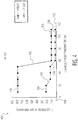
- Figure 4 are example near-field signals 400 from the example second application 300 of the set of near-field devices 102, 110.
- This Figure shows an example set of effects on the received near-field signal 304 (i.e. magnetic and electric fields) due to the degradation 302 of some sort between the 50 cm and 60 cm locations along the conductive structure 106.
- the degradation 302 to the conductive structure 106 in this example is detectable by the decoder circuit in the second near-field device 110 by a difference between the previously received H-Field 124 and/or E-Field 126 (see Figure 2 ) before the degradation 302 and the received H-Field 306 and/or E-Field 308 (see Figure 4 ) after the degradation 302.
- the H-Field fall-off 402 (i.e. magnetic field component) and the E-Field fall-off 404 (i.e. electric field component) can be due to flux attenuation at the degradation 302 location.
- Figure 5 is an example third application 500 of the set of near-field devices 102, 110.
- the example third application 500 includes the first near-field device 102 positioned at a first location 502 along a conductive structure 506 (e.g. inside of a metal pipe) and separated from the conductive structure 506 (e.g. inside of a metal pipe) by a dielectric 504 (e.g. air-gap for capacitive coupling).
- a conductive structure 506 e.g. inside of a metal pipe
- a dielectric 504 e.g. air-gap for capacitive coupling
- the example third application 500 also includes the second near-field device 110 positioned at a second location 508 along the conductive structure 506 and separated from the conductive structure 506 by a dielectric 510.
- the first near-field device 102 generates a transmitted near-field signal 512 having an H-Field 514 (i.e. magnetic field component) and an E-Field 516 (i.e. electric field component).
- the second near-field device 110 receives a near-field signal 518 having an H-Field 520 (i.e. magnetic field component) and an E-Field 522 (i.e. electric field component).
- Figure 6 is an example fourth application 600 of the set of near-field devices 102, 110.
- the example fourth application 600 includes the first near-field device 102 positioned at a first location 602 along a conductive structure 606 (e.g. metal plate) and separated from the conductive structure 606 by dielectric 604.
- a conductive structure 606 e.g. metal plate
- the example fourth application 600 also includes the second near-field device 110 positioned at a second location 608 along the conductive structure 606 and separated from the conductive structure 606 by dielectric 610.
- the first near-field device 102 generates a transmitted near-field signal having an H-Field 614 (i.e. magnetic field component) and an E-Field 616 (i.e. electric field component).
- the second near-field device 110 receives a near-field signal having an H-Field 620 (i.e. magnetic field component) and an E-Field 622 (i.e. electric field component).
- Figure 7A is an example side view of a fifth application 700 of the set of near-field devices 102, 110.
- Figure 7B is an example top view of the fifth application 700 of the set of near-field devices 102, 110.
- the conductive structure 712 is a container, such as a metal box, or a secure medical container.
- the example fifth application 700 includes the first near-field device 102 positioned at a first location 702 outside of a conductive structure 710 (e.g. metal container) and separated from the conductive structure 710 by dielectric 704.
- the second near-field device 110 is positioned at a second location 706 inside the conductive structure 710 and separated from the conductive structure 710 by dielectric 708.
- An opening 712 between the inside and outside of the conductive structure 710 permits near-field signals to pass from the first near-field device 102 to the second near-field device 110. However, the opening 712 in some example embodiments blocks RF radiation from passing between the inside and outside of the conductive structure 710.
- the conductive structure 712 substantially forms a Faraday Cage, thereby blocking RF radiation, but the opening 712 however permits near-field signals to pass.
- the near-field devices 102, 110 are positioned close to the opening 712 for better signal reception.
- Figure 8 is an example link-budget table 800 for the near-field signals communicating through the opening 712 in the example fifth application 700.
- the example link-budget table 800 shows signal strength losses in dB for variously sized conductive structures 712 (e.g. metal containers).
- link budgets 806 Shown in the table 800 are example link budgets 806 for various metal box sizes 802 and openings 804.
- the near-field devices 102, 110 were placed close to the opening 712.
- a near-field device including: a near-field receiver coupled to a near-field receiver antenna and a decoder circuit; wherein the near-field receiver antenna is configured to be capacitively coupled at a first location on a conductive structure; wherein the near-field receiver antenna is configured to receive a near-field signal from the conductive structure through the receiver's capacitive coupling; and wherein the decoder circuit is configured to detect variations in the near-field signal.
Landscapes
- Engineering & Computer Science (AREA)
- Computer Networks & Wireless Communication (AREA)
- Signal Processing (AREA)
- Chemical & Material Sciences (AREA)
- Chemical Kinetics & Catalysis (AREA)
- Electrochemistry (AREA)
- Physics & Mathematics (AREA)
- Health & Medical Sciences (AREA)
- Life Sciences & Earth Sciences (AREA)
- Analytical Chemistry (AREA)
- Biochemistry (AREA)
- General Health & Medical Sciences (AREA)
- General Physics & Mathematics (AREA)
- Immunology (AREA)
- Pathology (AREA)
- Near-Field Transmission Systems (AREA)
Abstract
Description
- The present specification relates to systems, methods, apparatuses, devices, articles of manufacture and instructions for near-field signal analysis.
- According to an example embodiment, a near-field device, comprising: a near-field receiver coupled to a near-field receiver antenna and a decoder circuit; wherein the near-field receiver antenna is configured to be capacitively coupled at a first location on a conductive structure; wherein the near-field receiver antenna is configured to receive a near-field signal from the conductive structure through the receiver's capacitive coupling; and wherein the decoder circuit is configured to detect variations in the near-field signal.
- In another example embodiment, another near-field device including a near-field transmitter is coupled to a near-field transmitter antenna and an encoder circuit; wherein the near-field transmitter antenna is configured to be capacitively coupled at a second location on the conductive structure; wherein the encoder circuit is configured to generate the near-field signal; and wherein the near-field transmitter antenna is configured to transmit the near-field signal to the conductive structure through the transmitter's capacitive coupling.
- In another example embodiment, the near-field transmitter antenna is separated from the near-field receiver antenna by greater than two centimeters.
- In another example embodiment, the near-field receiver antenna is configured to be capacitively coupled to the conductive structure using an air-gap between the conductive structure and an outside of the near-field device.
- In another example embodiment, the near-field signal includes a carrier frequency that is ≤ 40 MHz.
- In another example embodiment, the conductive structure includes at least one of: a pipe, a planar surface, a building girder, a vehicle chassis, a container, a metal box, a medicine bottle, a food package, a wire, or a tube.
- In another example embodiment, the conductive structure includes a conductive material including at least one of: iron, copper, or carbon.
- In another example embodiment, the conductive structure is a container having an inside and an outside; the container blocks RF radiation from entering the inside; and the container passes the near-field signal to the inside.
- In another example embodiment, the container further includes an opening; the container passes the near-field signal to the inside through the opening; and the opening does not pass RF radiation.
- In another example embodiment, the conductive structure is a container having an inside and an outside; the container blocks RF radiation from entering the inside; the container passes the near-field signal to the inside; and one of the near-field devices is outside of the container and one of the near-field devices is inside of the container.
- In another example embodiment, the decoder circuit includes a degradation detector configured to interpret the variations in the near-field signal as a structural degradation in the conductive structure.
- In another example embodiment, the structural degradation includes at least one of: a crack, a break, a bend, application of a coating to the conductive structure, a discontinuity, or an abnormal change in conductivity.
- In another example embodiment, the degradation detector is configured to interpret the variations in the near-field signal as indicating a structural degradation if there is a difference between a previously received H-Field signal and a currently received H-Field signal.
- In another example embodiment, the degradation detector is configured to interpret the variations in the near-field signal as indicating a structural degradation if there is a difference between a previously received E-Field signal and a currently received E-Field signal.
- In another example embodiment, the decoder circuit includes a communications circuit configured to interpret the variations in the near-field signal as a communications signal transmitted by another near-field device.
- According to an example embodiment, a method of processing a near-field signal, comprising: capacitively coupling a near-field device at a first location on a conductive structure; receiving a near-field signal at the near-field device from the conductive structure through the capacitive coupling; and detecting variations in the near-field signal.
- In another example embodiment, capacitively coupling another near-field device at a second location on the conductive structure; and transmitting the near-field signal at the another near-field device to the conductive structure through the capacitive coupling of the another near-field device.
- In another example embodiment, interpreting the variations in the near-field signal as a structural degradation in the conductive structure.
- In another example embodiment, interpreting the variations in the near-field signal as a communications signal transmitted by another near-field device.
- The above discussion is not intended to represent every example embodiment or every implementation within the scope of the current or future Claim sets. The Figures and Detailed Description that follow also exemplify various example embodiments.
- Various example embodiments may be more completely understood in consideration of the following Detailed Description in connection with the accompanying Drawings, in which:
-
-
Figure 1 is an example first application of a set of near-field devices. -
Figure 2 are example near-field signals from the example first application of the set of near-field devices. -
Figure 3 is an example second application of the set of near-field devices. -
Figure 4 are example near-field signals from the example second application of the set of near-field devices. -
Figure 5 is an example third application of the set of near-field devices. -
Figure 6 is an example fourth application of the set of near-field devices. -
Figure 7A is an example side view of a fifth application of the set of near-field devices. -
Figure 7B is an example top view of the fifth application of the set of near-field devices. -
Figure 8 is an example link-budget table for the near-field signals communicating through an opening from the example fifth application of the set of near-field devices. - While the disclosure is amenable to various modifications and alternative forms, specifics thereof have been shown by way of example in the drawings and will be described in detail. It should be understood, however, that other embodiments, beyond the particular embodiments described, are possible as well. All modifications, equivalents, and alternative embodiments falling within the spirit and scope of the appended claims are covered as well.
- Whereas RF wireless communication may be accomplished by propagating an RF plane wave through free space, near-field electromagnetic induction (NFEMI) devices utilize non-propagating quasi-static fields. The quasi-static characteristic of the fields is the result of antenna dimensions in combination with the carrier frequency. The majority of the energy is stored in the form of magnetic and electric fields and only a small amount of RF energy propagates in free space.
- Small antenna geometries compared with the carrier wavelength are candidate for near field communication since they do not generate radiating waves in free space. Such an antenna can be a coil antenna that allows near field magnetic induction (NFMI). Other antennas communicate by means of both magnetic (H) and electric (E) near-fields via near field electromagnetic induction (NFEMI).
- To be discussed herein are example embodiments of a near-field electromagnetic induction (NFEMI) device which when capacitively coupled to a conductive structure can be used to communication or perform conductive structure integrity checks by means of a combination of magnetic and electric near-fields.
- For example, two communication devices which each include near-field devices, can be positioned at different locations along a conductive structure and are able both wireless communicate with each other and detect any stresses or damages to the conductive structure.
- Various embodiments of the near-field device may include: control circuitry, microprocessors, microcontrollers, digital signal processors, data processing units, human interface units, and antennas. Such antennas when in close proximity to a conductive structure will generate fields that are substantially confined near the conductive structure, thus providing a strong near-field signal for either communication or conductive structure integrity checks.
- The near-field device to be discussed can be used in different possible applications, including industrial applications. For example the near-field device can be used to communicate with sensors inside a secure conductive container perhaps including medicine or food, and/or communicate at distances over conductive structures such as: metal pipes, building girders or I-beams, even if encased in concrete.
-
Figure 1 is an examplefirst application 100 of a set of near-field devices first application 100 includes the first near-field device 102 (e.g. for near-field signal transmission and/or reception) positioned at afirst location 104 along aconductive structure 106. The first near-field device 102 includes a near-field transmitter antenna (not shown), a transmitter circuit (not shown), an encoder circuit (not shown) and is separated from theconductive structure 106 by a dielectric 108 (e.g. air-gap for capacitive coupling). - The example
first application 100 also includes a second near-field device 110 (e.g. for near-field signal reception and/or transmission) positioned at asecond location 112 along theconductive structure 106. The second near-field device 110 includes a near-field receiver antenna (not shown), a receiver circuit (not shown), a decoder circuit (not shown) and a dielectric 114 (e.g. air-gap for capacitive coupling). - The first near-
field device 102 uses the encoder to generate a transmitted near-field signal 116 having an H-Field 118 (i.e. magnetic field) component and an E-Field 120 (i.e. electric field) component. The first near-field device 102 transmits the near-field signal 116 to theconductive structure 106 through the transmitter's dielectric 108 (i.e. capacitive coupling). - The second near-
field device 110 receives a near-field signal 122 from theconductive structure 106 through the receiver's dielectric 114 (i.e. capacitive coupling). This received near-field signal 122 corresponds to the transmitted near-field signal 116, but due to variations over theconductive structure 106, has an H-Field 124 (i.e. magnetic field) component and an E-Field 126 (i.e. electric field) component, which may or may not differ from the H-Field 118 andE-Field 120 components. - The H-
field Figure 1 illustrate the magnetic and electric near-fields along theconductive structure 106. The near-field transmitter antenna is designed so that the magnetic field is curved around theconductive structure 106. The electric field vector is perpendicular to theconductive structure 106 since the tube is conductive. The magnetic field and the electric field are distributed over the length of theconductive structure 106. The antenna of the second near-field device 110 is able to convert both H and E fields into voltages that can be processed by the receiver circuit in the second near-field device 110. - In some example embodiments, the
dielectrics conductive structure 106 and the outside of the near-field devices - The decoder circuit in the second near-
field device 110 detects and interprets these variations in the near-field signal 122. In thisfirst application 100 and in further example embodiments (see below), the near-field devices field devices - The near-field transmitter antenna can be separated from the near-field receiver antenna over a range of distances (e.g. 20cm to several meters).
- In some NFMI and NFEMI embodiments, the near-field signal includes a carrier frequency that is below 30 MHz; however, other embodiments can use other carrier frequencies that permit near-field operation.
- The
conductive structure 106 in various embodiments can be at least one of: a pipe, a planar surface, a building girder, a vehicle chassis, a container, a metal box, a medicine bottle, a food package, a wire, or a tube. The near-field devices conductive structures 106. Theconductive structure 106 can also be fabricated from a variety of conductive materials, including: iron, copper, or carbon. -
Figure 2 are example near-field signals 200 from the examplefirst application 100 of the set of near-field devices Figure 1 . In is example 200 thefirst location 104 is at 0 cm and thesecond location 112 is at 120 cm. As the conductive properties of theconductive structure 106 decrease the H-field remains linear (if no breaks) but shifts "down" and E-field slants down as distance from the first near-field device 102 (e.g. transmitter) increases. -
Figure 2 shows an example baseline reading for the magnetic and electric fields over the length of theconductive structure 106 at a first point in time. Subsequent readings at a later time can show degradation in theconductive structure 106, as will be discussed inFigure 4 . In this example, at less than 20 cm from the first near-field device 102, H-fields and E-fields are very complex so no integrity measurements here. However, a revised NFEMI antenna could reduce this region of complexity to less than 20 cm. -
Figure 3 is an examplesecond application 300 of the set of near-field devices second application 300 the near-field devices conductive structure 106 if there is a difference between a previously received near-field signal 122 and a currently near-field signal 304. - The first near-
field device 102 in this example 300 continues to generate a transmitted near-field signal 116 having an H-Field 118 (i.e. magnetic field) component and an E-Field 120 (i.e. electric field) component. However, the second near-field device 110 receives a degraded near-field signal 304 having an H-Field 306 (i.e. magnetic field) component and an E-Field 308 (i.e. electric field) component substantially less than the H-Field 118 and E-Field 120 components. This is due to thedegradation 302 along theconductive structure 106. - In some example embodiments, the structural degradation includes at least one of: a crack, a break, a bend, application of a coating to the conductive structure, a discontinuity, or abrupt change in conductivity.
- Thus the set of near-
field devices field devices -
Figure 4 are example near-field signals 400 from the examplesecond application 300 of the set of near-field devices degradation 302 of some sort between the 50 cm and 60 cm locations along theconductive structure 106. - The
degradation 302 to theconductive structure 106 in this example is detectable by the decoder circuit in the second near-field device 110 by a difference between the previously received H-Field 124 and/or E-Field 126 (seeFigure 2 ) before thedegradation 302 and the received H-Field 306 and/or E-Field 308 (seeFigure 4 ) after thedegradation 302. The H-Field fall-off 402 (i.e. magnetic field component) and the E-Field fall-off 404 (i.e. electric field component) can be due to flux attenuation at thedegradation 302 location. -
Figure 5 is an examplethird application 500 of the set of near-field devices third application 500 includes the first near-field device 102 positioned at afirst location 502 along a conductive structure 506 (e.g. inside of a metal pipe) and separated from the conductive structure 506 (e.g. inside of a metal pipe) by a dielectric 504 (e.g. air-gap for capacitive coupling). - The example
third application 500 also includes the second near-field device 110 positioned at asecond location 508 along theconductive structure 506 and separated from theconductive structure 506 by a dielectric 510. - The first near-
field device 102 generates a transmitted near-field signal 512 having an H-Field 514 (i.e. magnetic field component) and an E-Field 516 (i.e. electric field component). The second near-field device 110 receives a near-field signal 518 having an H-Field 520 (i.e. magnetic field component) and an E-Field 522 (i.e. electric field component). -
Figure 6 is an examplefourth application 600 of the set of near-field devices fourth application 600 includes the first near-field device 102 positioned at afirst location 602 along a conductive structure 606 (e.g. metal plate) and separated from theconductive structure 606 bydielectric 604. - The example
fourth application 600 also includes the second near-field device 110 positioned at asecond location 608 along theconductive structure 606 and separated from theconductive structure 606 bydielectric 610. - The first near-
field device 102 generates a transmitted near-field signal having an H-Field 614 (i.e. magnetic field component) and an E-Field 616 (i.e. electric field component). The second near-field device 110 receives a near-field signal having an H-Field 620 (i.e. magnetic field component) and an E-Field 622 (i.e. electric field component). -
Figure 7A is an example side view of afifth application 700 of the set of near-field devices Figure 7B is an example top view of thefifth application 700 of the set of near-field devices conductive structure 712 is a container, such as a metal box, or a secure medical container. - The example
fifth application 700 includes the first near-field device 102 positioned at afirst location 702 outside of a conductive structure 710 (e.g. metal container) and separated from theconductive structure 710 bydielectric 704. The second near-field device 110 is positioned at asecond location 706 inside theconductive structure 710 and separated from theconductive structure 710 bydielectric 708. - An
opening 712 between the inside and outside of theconductive structure 710 permits near-field signals to pass from the first near-field device 102 to the second near-field device 110. However, theopening 712 in some example embodiments blocks RF radiation from passing between the inside and outside of theconductive structure 710. - In some example embodiments, the
conductive structure 712 substantially forms a Faraday Cage, thereby blocking RF radiation, but theopening 712 however permits near-field signals to pass. In some example embodiments, the near-field devices opening 712 for better signal reception. -
Figure 8 is an example link-budget table 800 for the near-field signals communicating through theopening 712 in the examplefifth application 700. The example link-budget table 800 shows signal strength losses in dB for variously sized conductive structures 712 (e.g. metal containers). - Shown in the table 800 are
example link budgets 806 for variousmetal box sizes 802 and openings 804. In this example, the near-field devices opening 712. The link budget is defined by: Link Budget
- Herein is disclosed, a near-field device, including: a near-field receiver coupled to a near-field receiver antenna and a decoder circuit; wherein the near-field receiver antenna is configured to be capacitively coupled at a first location on a conductive structure; wherein the near-field receiver antenna is configured to receive a near-field signal from the conductive structure through the receiver's capacitive coupling; and wherein the decoder circuit is configured to detect variations in the near-field signal.
- It will be readily understood that the components of the embodiments as generally described herein and illustrated in the appended figures could be arranged and designed in a wide variety of different configurations. Thus, the detailed description of various embodiments, as represented in the figures, is not intended to limit the scope of the present disclosure, but is merely representative of various embodiments. While the various aspects of the embodiments are presented in drawings, the drawings are not necessarily drawn to scale unless specifically indicated.
- The present invention may be embodied in other specific forms without departing from its spirit or essential characteristics. The described embodiments are to be considered in all respects only as illustrative and not restrictive. The scope of the invention is, therefore, indicated by the appended claims rather than by this detailed description. All changes which come within the meaning and range of equivalency of the claims are to be embraced within their scope.
- Reference throughout this specification to features, advantages, or similar language does not imply that all of the features and advantages that may be realized with the present invention should be or are in any single embodiment of the invention. Rather, language referring to the features and advantages is understood to mean that a specific feature, advantage, or characteristic described in connection with an embodiment is included in at least one embodiment of the present invention. Thus, discussions of the features and advantages, and similar language, throughout this specification may, but do not necessarily, refer to the same embodiment.
- Furthermore, the described features, advantages, and characteristics of the invention may be combined in any suitable manner in one or more embodiments. One skilled in the relevant art will recognize, in light of the description herein, that the invention can be practiced without one or more of the specific features or advantages of a particular embodiment. In other instances, additional features and advantages may be recognized in certain embodiments that may not be present in all embodiments of the invention.
- Reference throughout this specification to "one embodiment," "an embodiment," or similar language means that a particular feature, structure, or characteristic described in connection with the indicated embodiment is included in at least one embodiment of the present invention. Thus, the phrases "in one embodiment," "in an embodiment," and similar language throughout this specification may, but do not necessarily, all refer to the same embodiment.
Claims (15)
- A near-field device, comprising:a near-field receiver coupled to a near-field receiver antenna and a decoder circuit;wherein the near-field receiver antenna is configured to be capacitively coupled at a first location on a conductive structure;wherein the near-field receiver antenna is configured to receive a near-field signal from the conductive structure through the receiver's capacitive coupling; andwherein the decoder circuit is configured to detect variations in the near-field signal.
- The device of claim 1, further comprising:another near-field device including a near-field transmitter coupled to a near-field transmitter antenna and an encoder circuit;wherein the near-field transmitter antenna is configured to be capacitively coupled at a second location on the conductive structure;wherein the encoder circuit is configured to generate the near-field signal; andwherein the near-field transmitter antenna is configured to transmit the near-field signal to the conductive structure through the transmitter's capacitive coupling.
- The device of claims 1 or 2:
wherein the near-field transmitter antenna is separated from the near-field receiver antenna by greater than two centimeters. - The device of any preceding claim:
wherein the near-field receiver antenna is configured to be capacitively coupled to the conductive structure using an air-gap between the conductive structure and an outside of the near-field device. - The device of any preceding claim:
wherein the near-field signal includes a carrier frequency that is less than or equal to 40 MHz. - The device of any preceding claim:
wherein the conductive structure includes at least one of: a pipe, a planar surface, a building girder, a vehicle chassis, a container, a metal box, a medicine bottle, a food package, a wire, or a tube. - The device of any preceding claim:
wherein the conductive structure includes a conductive material including at least one of: iron, copper, or carbon. - The device of any preceding claim:wherein the conductive structure is a container having an inside and an outside;wherein the container blocks RF radiation from entering the inside; andwherein the container passes the near-field signal to the inside.
- The device of claim 8:wherein the container further includes an opening;wherein the container passes the near-field signal to the inside through the opening; andwherein the opening does not pass RF radiation.
- The device of claims 8 or 9:
wherein one of the near-field devices is outside of the container and one of the near-field devices is inside of the container. - The device of any preceding claim:
wherein the decoder circuit includes a degradation detector configured to interpret the variations in the near-field signal as a structural degradation in the conductive structure. - The device of claim 11:
wherein the structural degradation includes at least one of: a crack, a break, a bend, application of a coating to the conductive structure, a discontinuity, or an abnormal change in conductivity. - The device of claim 11 or 12:
wherein the degradation detector is configured to interpret the variations in the near-field signal as indicating a structural degradation if there is a difference between a previously received H-Field signal and a currently received H-Field signal. - The device of any of claims 11 to 13:
wherein the degradation detector is configured to interpret the variations in the near-field signal as indicating a structural degradation if there is a difference between a previously received E-Field signal and a currently received E-Field signal. - The device of any preceding claim:
wherein the decoder circuit includes a communications circuit configured to interpret the variations in the near-field signal as a communications signal transmitted by another near-field device.
Applications Claiming Priority (1)
| Application Number | Priority Date | Filing Date | Title |
|---|---|---|---|
| US15/602,160 US10965346B2 (en) | 2017-05-23 | 2017-05-23 | Near-field device |
Publications (2)
| Publication Number | Publication Date |
|---|---|
| EP3407504A1 true EP3407504A1 (en) | 2018-11-28 |
| EP3407504B1 EP3407504B1 (en) | 2021-03-31 |
Family
ID=62528239
Family Applications (1)
| Application Number | Title | Priority Date | Filing Date |
|---|---|---|---|
| EP18173396.5A Active EP3407504B1 (en) | 2017-05-23 | 2018-05-21 | Near-field device |
Country Status (3)
| Country | Link |
|---|---|
| US (1) | US10965346B2 (en) |
| EP (1) | EP3407504B1 (en) |
| CN (1) | CN108933615B (en) |
Families Citing this family (2)
| Publication number | Priority date | Publication date | Assignee | Title |
|---|---|---|---|---|
| US11115069B2 (en) * | 2020-01-24 | 2021-09-07 | Nxp B.V. | Near-field wireless device for distance measurement |
| US20240147555A1 (en) * | 2021-03-26 | 2024-05-02 | Sony Group Corporation | Communication system and communication method |
Citations (2)
| Publication number | Priority date | Publication date | Assignee | Title |
|---|---|---|---|---|
| US20060063488A1 (en) * | 2002-10-11 | 2006-03-23 | Siemens Aktiengesellschaft | Asymmetric information transmission system using an electric near field |
| US20160110639A1 (en) * | 2014-08-10 | 2016-04-21 | David Finn | Passive smart cards, metal cards, payment objects and smart jewelry |
Family Cites Families (24)
| Publication number | Priority date | Publication date | Assignee | Title |
|---|---|---|---|---|
| US2438795A (en) | 1943-12-13 | 1948-03-30 | Hazeltine Research Inc | Wave-guide system |
| BE554252A (en) | 1950-03-21 | |||
| US4639669A (en) | 1983-09-26 | 1987-01-27 | Lockheed Missiles & Space Company, Inc. | Pulsed electromagnetic nondestructive test method for determining volume density of graphite fibers in a graphite-epoxy composite material |
| US4743916A (en) | 1985-12-24 | 1988-05-10 | The Boeing Company | Method and apparatus for proportional RF radiation from surface wave transmission line |
| JPH04361168A (en) | 1991-06-08 | 1992-12-14 | Horiba Ltd | Electromagnetic induction type conductivity meter |
| US5341100A (en) | 1992-12-22 | 1994-08-23 | Western Atlas International, Inc. | Electromagnetic wave method and apparatus for downhole measurement of fluid conductivity and hydrocarbon volume during formation testing |
| GB9600541D0 (en) | 1996-01-11 | 1996-03-13 | Cambridge Consultants | Method of measuring an electrical property |
| DE19628690C2 (en) | 1996-07-17 | 1999-04-22 | Achenbach Buschhuetten Gmbh | Methods and measuring systems for measuring physical quantities of low conductivity and non-conductivity fluids |
| US6691563B1 (en) | 2000-04-11 | 2004-02-17 | The United States Of America As Represented By The Department Of Agriculture | Universal dielectric calibration method and apparatus for moisture content determination in particulate and granular materials |
| US6627461B2 (en) * | 2001-04-18 | 2003-09-30 | Signature Bioscience, Inc. | Method and apparatus for detection of molecular events using temperature control of detection environment |
| CN1774836B (en) | 2002-12-09 | 2010-09-08 | 科里多系统公司 | Method and device for emitting surface waves to a single conductor transmission line |
| US7567154B2 (en) | 2004-05-21 | 2009-07-28 | Corridor Systems, Inc. | Surface wave transmission system over a single conductor having E-fields terminating along the conductor |
| CN1710412A (en) | 2004-06-17 | 2005-12-21 | 昆明金汇通无线与微波技术研究所 | Method for detecting substance content and component |
| US7440858B2 (en) * | 2005-04-15 | 2008-10-21 | Lawrence Livermore National Security, Llc | Poynting-vector based method for determining the bearing and location of electromagnetic sources |
| EP1949084B1 (en) * | 2005-07-06 | 2014-09-10 | Ferlin Medical Ltd | Apparatus and method for measuring constituent concentrations within a biological tissue structure |
| WO2007028035A2 (en) * | 2005-09-01 | 2007-03-08 | Proteus Biomedical, Inc. | Implantable zero-wire communications system |
| DE602006016645D1 (en) | 2005-12-19 | 2010-10-14 | Nxp Bv | RADIO RECEIVER, RADIO TRANSMITTER AND HEARING DEVICE |
| IT1394915B1 (en) | 2009-07-21 | 2012-07-20 | Pietro Fiorentini Spa | DEVICE FOR THE MEASUREMENT OF ELECTRICAL FLUID AND METHOD PROPERTIES TO MEASURE THESE ELECTRICAL PROPERTIES |
| US9197956B2 (en) | 2013-09-04 | 2015-11-24 | Etymotic Research, Inc. | Comformable eartip |
| EP2858259B1 (en) * | 2013-10-07 | 2019-06-26 | Nxp B.V. | NFC tag, communication method and system |
| US8897697B1 (en) | 2013-11-06 | 2014-11-25 | At&T Intellectual Property I, Lp | Millimeter-wave surface-wave communications |
| US9197986B1 (en) | 2014-06-12 | 2015-11-24 | Nxp, B.V. | Electromagnetic induction radio |
| US9753072B2 (en) | 2014-08-14 | 2017-09-05 | The Boeing Company | Magnetic coupling for electrical conductivity assessment |
| CN104655656B (en) | 2014-12-05 | 2018-07-13 | 广州丰谱信息技术有限公司 | Detection imaging method and device based on wideband magnetic wave transmission model parameter identification |
-
2017
- 2017-05-23 US US15/602,160 patent/US10965346B2/en active Active
-
2018
- 2018-05-21 EP EP18173396.5A patent/EP3407504B1/en active Active
- 2018-05-23 CN CN201810504872.XA patent/CN108933615B/en active Active
Patent Citations (2)
| Publication number | Priority date | Publication date | Assignee | Title |
|---|---|---|---|---|
| US20060063488A1 (en) * | 2002-10-11 | 2006-03-23 | Siemens Aktiengesellschaft | Asymmetric information transmission system using an electric near field |
| US20160110639A1 (en) * | 2014-08-10 | 2016-04-21 | David Finn | Passive smart cards, metal cards, payment objects and smart jewelry |
Non-Patent Citations (2)
| Title |
|---|
| DIAMOND G ET AL: "A New Capacitive Imaging Technique for NDT", 1 November 2006 (2006-11-01), pages 1 - 8, XP002516729, Retrieved from the Internet <URL:http://www.ndt.net/article/ecndt2006/doc/P229.pdf> [retrieved on 20061101] * |
| LIU ZHENG ET AL: "Experimenting capacitive sensing technique for structural integrity assessment", 2017 IEEE INTERNATIONAL CONFERENCE ON INDUSTRIAL TECHNOLOGY (ICIT), IEEE, 22 March 2017 (2017-03-22), pages 922 - 927, XP033091229, DOI: 10.1109/ICIT.2017.7915483 * |
Also Published As
| Publication number | Publication date |
|---|---|
| US10965346B2 (en) | 2021-03-30 |
| EP3407504B1 (en) | 2021-03-31 |
| CN108933615B (en) | 2022-08-09 |
| CN108933615A (en) | 2018-12-04 |
| US20180343035A1 (en) | 2018-11-29 |
Similar Documents
| Publication | Publication Date | Title |
|---|---|---|
| US20130009803A1 (en) | Multi-channel radar level gauge | |
| EP2701283A1 (en) | Resonance-type non-contact power supply system | |
| CN105049130B (en) | Wireless communication distance test device and method | |
| CN102763278A (en) | Leaky coaxial cable | |
| EP3407504A1 (en) | Near-field device | |
| JP7328584B2 (en) | Non-powered relay device and non-powered relay method | |
| US12273735B2 (en) | Apparatus, methods and systems for improving coverage of wireless communication networks | |
| JP6179969B2 (en) | System for determining whether radio coverage is possible | |
| EP3574332B1 (en) | System for testing wireless communication equipment employing antennas | |
| US8373546B2 (en) | Mobile body remote control system | |
| CN106949860B (en) | Pipeline inner wall detection system and method | |
| Trueman et al. | Comparison of computed RF current flow on a power line with full scale measurements | |
| Bryakin et al. | Cable avoidance tool | |
| CN203164312U (en) | Testing system for measuring directional diagram of iron tower of power transmission line | |
| CN105223556A (en) | L-type transmitting-receiving array antenna front end and signal processing method thereof | |
| RU2439589C1 (en) | Real-time measurement device for current control in high-voltage power networks | |
| US8311752B1 (en) | Method and apparatus to quantify mast clamp current probe effective loss on pole-mast antenna | |
| CN208818764U (en) | Electric field probe | |
| JPH11331099A (en) | Reception method and device in communication system using magnetic vector potential | |
| JP3080345B2 (en) | Signal transmission device for mobile objects | |
| HE et al. | Dipole antenna reception of transient electromagnetic fields refracted from a dipole antenna buried in a lossy half-space | |
| Peng et al. | A novel 1-dimensional object location estimation algorithm using leaky coaxial cable | |
| Fox | Broadband over power lines (BPL) interference analysis | |
| US20220003688A1 (en) | Surface Change Detector and Surface Change Detection Method Using Same | |
| CN106018979A (en) | FM radiation intensity testing system for vehicle FM intelligent device |
Legal Events
| Date | Code | Title | Description |
|---|---|---|---|
| PUAI | Public reference made under article 153(3) epc to a published international application that has entered the european phase |
Free format text: ORIGINAL CODE: 0009012 |
|
| STAA | Information on the status of an ep patent application or granted ep patent |
Free format text: STATUS: THE APPLICATION HAS BEEN PUBLISHED |
|
| AK | Designated contracting states |
Kind code of ref document: A1 Designated state(s): AL AT BE BG CH CY CZ DE DK EE ES FI FR GB GR HR HU IE IS IT LI LT LU LV MC MK MT NL NO PL PT RO RS SE SI SK SM TR |
|
| AX | Request for extension of the european patent |
Extension state: BA ME |
|
| STAA | Information on the status of an ep patent application or granted ep patent |
Free format text: STATUS: REQUEST FOR EXAMINATION WAS MADE |
|
| 17P | Request for examination filed |
Effective date: 20190528 |
|
| RBV | Designated contracting states (corrected) |
Designated state(s): AL AT BE BG CH CY CZ DE DK EE ES FI FR GB GR HR HU IE IS IT LI LT LU LV MC MK MT NL NO PL PT RO RS SE SI SK SM TR |
|
| STAA | Information on the status of an ep patent application or granted ep patent |
Free format text: STATUS: EXAMINATION IS IN PROGRESS |
|
| 17Q | First examination report despatched |
Effective date: 20200507 |
|
| GRAP | Despatch of communication of intention to grant a patent |
Free format text: ORIGINAL CODE: EPIDOSNIGR1 |
|
| STAA | Information on the status of an ep patent application or granted ep patent |
Free format text: STATUS: GRANT OF PATENT IS INTENDED |
|
| INTG | Intention to grant announced |
Effective date: 20201026 |
|
| GRAJ | Information related to disapproval of communication of intention to grant by the applicant or resumption of examination proceedings by the epo deleted |
Free format text: ORIGINAL CODE: EPIDOSDIGR1 |
|
| STAA | Information on the status of an ep patent application or granted ep patent |
Free format text: STATUS: EXAMINATION IS IN PROGRESS |
|
| GRAJ | Information related to disapproval of communication of intention to grant by the applicant or resumption of examination proceedings by the epo deleted |
Free format text: ORIGINAL CODE: EPIDOSDIGR1 |
|
| GRAS | Grant fee paid |
Free format text: ORIGINAL CODE: EPIDOSNIGR3 |
|
| STAA | Information on the status of an ep patent application or granted ep patent |
Free format text: STATUS: GRANT OF PATENT IS INTENDED |
|
| GRAP | Despatch of communication of intention to grant a patent |
Free format text: ORIGINAL CODE: EPIDOSNIGR1 |
|
| GRAA | (expected) grant |
Free format text: ORIGINAL CODE: 0009210 |
|
| STAA | Information on the status of an ep patent application or granted ep patent |
Free format text: STATUS: THE PATENT HAS BEEN GRANTED |
|
| INTC | Intention to grant announced (deleted) | ||
| INTG | Intention to grant announced |
Effective date: 20210222 |
|
| AK | Designated contracting states |
Kind code of ref document: B1 Designated state(s): AL AT BE BG CH CY CZ DE DK EE ES FI FR GB GR HR HU IE IS IT LI LT LU LV MC MK MT NL NO PL PT RO RS SE SI SK SM TR |
|
| REG | Reference to a national code |
Ref country code: GB Ref legal event code: FG4D Ref country code: CH Ref legal event code: EP |
|
| REG | Reference to a national code |
Ref country code: AT Ref legal event code: REF Ref document number: 1378111 Country of ref document: AT Kind code of ref document: T Effective date: 20210415 |
|
| REG | Reference to a national code |
Ref country code: DE Ref legal event code: R096 Ref document number: 602018014591 Country of ref document: DE |
|
| REG | Reference to a national code |
Ref country code: IE Ref legal event code: FG4D |
|
| REG | Reference to a national code |
Ref country code: LT Ref legal event code: MG9D |
|
| PG25 | Lapsed in a contracting state [announced via postgrant information from national office to epo] |
Ref country code: NO Free format text: LAPSE BECAUSE OF FAILURE TO SUBMIT A TRANSLATION OF THE DESCRIPTION OR TO PAY THE FEE WITHIN THE PRESCRIBED TIME-LIMIT Effective date: 20210630 Ref country code: FI Free format text: LAPSE BECAUSE OF FAILURE TO SUBMIT A TRANSLATION OF THE DESCRIPTION OR TO PAY THE FEE WITHIN THE PRESCRIBED TIME-LIMIT Effective date: 20210331 Ref country code: HR Free format text: LAPSE BECAUSE OF FAILURE TO SUBMIT A TRANSLATION OF THE DESCRIPTION OR TO PAY THE FEE WITHIN THE PRESCRIBED TIME-LIMIT Effective date: 20210331 Ref country code: BG Free format text: LAPSE BECAUSE OF FAILURE TO SUBMIT A TRANSLATION OF THE DESCRIPTION OR TO PAY THE FEE WITHIN THE PRESCRIBED TIME-LIMIT Effective date: 20210630 |
|
| PG25 | Lapsed in a contracting state [announced via postgrant information from national office to epo] |
Ref country code: LV Free format text: LAPSE BECAUSE OF FAILURE TO SUBMIT A TRANSLATION OF THE DESCRIPTION OR TO PAY THE FEE WITHIN THE PRESCRIBED TIME-LIMIT Effective date: 20210331 Ref country code: RS Free format text: LAPSE BECAUSE OF FAILURE TO SUBMIT A TRANSLATION OF THE DESCRIPTION OR TO PAY THE FEE WITHIN THE PRESCRIBED TIME-LIMIT Effective date: 20210331 Ref country code: SE Free format text: LAPSE BECAUSE OF FAILURE TO SUBMIT A TRANSLATION OF THE DESCRIPTION OR TO PAY THE FEE WITHIN THE PRESCRIBED TIME-LIMIT Effective date: 20210331 |
|
| REG | Reference to a national code |
Ref country code: NL Ref legal event code: MP Effective date: 20210331 |
|
| REG | Reference to a national code |
Ref country code: AT Ref legal event code: MK05 Ref document number: 1378111 Country of ref document: AT Kind code of ref document: T Effective date: 20210331 |
|
| PG25 | Lapsed in a contracting state [announced via postgrant information from national office to epo] |
Ref country code: LT Free format text: LAPSE BECAUSE OF FAILURE TO SUBMIT A TRANSLATION OF THE DESCRIPTION OR TO PAY THE FEE WITHIN THE PRESCRIBED TIME-LIMIT Effective date: 20210331 Ref country code: EE Free format text: LAPSE BECAUSE OF FAILURE TO SUBMIT A TRANSLATION OF THE DESCRIPTION OR TO PAY THE FEE WITHIN THE PRESCRIBED TIME-LIMIT Effective date: 20210331 Ref country code: CZ Free format text: LAPSE BECAUSE OF FAILURE TO SUBMIT A TRANSLATION OF THE DESCRIPTION OR TO PAY THE FEE WITHIN THE PRESCRIBED TIME-LIMIT Effective date: 20210331 Ref country code: NL Free format text: LAPSE BECAUSE OF FAILURE TO SUBMIT A TRANSLATION OF THE DESCRIPTION OR TO PAY THE FEE WITHIN THE PRESCRIBED TIME-LIMIT Effective date: 20210331 Ref country code: SM Free format text: LAPSE BECAUSE OF FAILURE TO SUBMIT A TRANSLATION OF THE DESCRIPTION OR TO PAY THE FEE WITHIN THE PRESCRIBED TIME-LIMIT Effective date: 20210331 Ref country code: AT Free format text: LAPSE BECAUSE OF FAILURE TO SUBMIT A TRANSLATION OF THE DESCRIPTION OR TO PAY THE FEE WITHIN THE PRESCRIBED TIME-LIMIT Effective date: 20210331 |
|
| PG25 | Lapsed in a contracting state [announced via postgrant information from national office to epo] |
Ref country code: PL Free format text: LAPSE BECAUSE OF FAILURE TO SUBMIT A TRANSLATION OF THE DESCRIPTION OR TO PAY THE FEE WITHIN THE PRESCRIBED TIME-LIMIT Effective date: 20210331 Ref country code: PT Free format text: LAPSE BECAUSE OF FAILURE TO SUBMIT A TRANSLATION OF THE DESCRIPTION OR TO PAY THE FEE WITHIN THE PRESCRIBED TIME-LIMIT Effective date: 20210802 Ref country code: SK Free format text: LAPSE BECAUSE OF FAILURE TO SUBMIT A TRANSLATION OF THE DESCRIPTION OR TO PAY THE FEE WITHIN THE PRESCRIBED TIME-LIMIT Effective date: 20210331 Ref country code: RO Free format text: LAPSE BECAUSE OF FAILURE TO SUBMIT A TRANSLATION OF THE DESCRIPTION OR TO PAY THE FEE WITHIN THE PRESCRIBED TIME-LIMIT Effective date: 20210331 Ref country code: IS Free format text: LAPSE BECAUSE OF FAILURE TO SUBMIT A TRANSLATION OF THE DESCRIPTION OR TO PAY THE FEE WITHIN THE PRESCRIBED TIME-LIMIT Effective date: 20210731 |
|
| REG | Reference to a national code |
Ref country code: CH Ref legal event code: PL |
|
| REG | Reference to a national code |
Ref country code: DE Ref legal event code: R097 Ref document number: 602018014591 Country of ref document: DE |
|
| PG25 | Lapsed in a contracting state [announced via postgrant information from national office to epo] |
Ref country code: ES Free format text: LAPSE BECAUSE OF FAILURE TO SUBMIT A TRANSLATION OF THE DESCRIPTION OR TO PAY THE FEE WITHIN THE PRESCRIBED TIME-LIMIT Effective date: 20210331 Ref country code: MC Free format text: LAPSE BECAUSE OF FAILURE TO SUBMIT A TRANSLATION OF THE DESCRIPTION OR TO PAY THE FEE WITHIN THE PRESCRIBED TIME-LIMIT Effective date: 20210331 Ref country code: LU Free format text: LAPSE BECAUSE OF NON-PAYMENT OF DUE FEES Effective date: 20210521 Ref country code: LI Free format text: LAPSE BECAUSE OF NON-PAYMENT OF DUE FEES Effective date: 20210531 Ref country code: AL Free format text: LAPSE BECAUSE OF FAILURE TO SUBMIT A TRANSLATION OF THE DESCRIPTION OR TO PAY THE FEE WITHIN THE PRESCRIBED TIME-LIMIT Effective date: 20210331 Ref country code: DK Free format text: LAPSE BECAUSE OF FAILURE TO SUBMIT A TRANSLATION OF THE DESCRIPTION OR TO PAY THE FEE WITHIN THE PRESCRIBED TIME-LIMIT Effective date: 20210331 Ref country code: CH Free format text: LAPSE BECAUSE OF NON-PAYMENT OF DUE FEES Effective date: 20210531 |
|
| PLBE | No opposition filed within time limit |
Free format text: ORIGINAL CODE: 0009261 |
|
| STAA | Information on the status of an ep patent application or granted ep patent |
Free format text: STATUS: NO OPPOSITION FILED WITHIN TIME LIMIT |
|
| REG | Reference to a national code |
Ref country code: BE Ref legal event code: MM Effective date: 20210531 |
|
| 26N | No opposition filed |
Effective date: 20220104 |
|
| PG25 | Lapsed in a contracting state [announced via postgrant information from national office to epo] |
Ref country code: IE Free format text: LAPSE BECAUSE OF NON-PAYMENT OF DUE FEES Effective date: 20210521 |
|
| PG25 | Lapsed in a contracting state [announced via postgrant information from national office to epo] |
Ref country code: IS Free format text: LAPSE BECAUSE OF FAILURE TO SUBMIT A TRANSLATION OF THE DESCRIPTION OR TO PAY THE FEE WITHIN THE PRESCRIBED TIME-LIMIT Effective date: 20210731 Ref country code: FR Free format text: LAPSE BECAUSE OF NON-PAYMENT OF DUE FEES Effective date: 20210531 |
|
| PG25 | Lapsed in a contracting state [announced via postgrant information from national office to epo] |
Ref country code: IT Free format text: LAPSE BECAUSE OF FAILURE TO SUBMIT A TRANSLATION OF THE DESCRIPTION OR TO PAY THE FEE WITHIN THE PRESCRIBED TIME-LIMIT Effective date: 20210331 Ref country code: BE Free format text: LAPSE BECAUSE OF NON-PAYMENT OF DUE FEES Effective date: 20210531 |
|
| GBPC | Gb: european patent ceased through non-payment of renewal fee |
Effective date: 20220521 |
|
| PG25 | Lapsed in a contracting state [announced via postgrant information from national office to epo] |
Ref country code: GB Free format text: LAPSE BECAUSE OF NON-PAYMENT OF DUE FEES Effective date: 20220521 |
|
| PG25 | Lapsed in a contracting state [announced via postgrant information from national office to epo] |
Ref country code: CY Free format text: LAPSE BECAUSE OF FAILURE TO SUBMIT A TRANSLATION OF THE DESCRIPTION OR TO PAY THE FEE WITHIN THE PRESCRIBED TIME-LIMIT Effective date: 20210331 |
|
| PG25 | Lapsed in a contracting state [announced via postgrant information from national office to epo] |
Ref country code: HU Free format text: LAPSE BECAUSE OF FAILURE TO SUBMIT A TRANSLATION OF THE DESCRIPTION OR TO PAY THE FEE WITHIN THE PRESCRIBED TIME-LIMIT; INVALID AB INITIO Effective date: 20180521 Ref country code: GR Free format text: LAPSE BECAUSE OF FAILURE TO SUBMIT A TRANSLATION OF THE DESCRIPTION OR TO PAY THE FEE WITHIN THE PRESCRIBED TIME-LIMIT Effective date: 20210331 |
|
| P01 | Opt-out of the competence of the unified patent court (upc) registered |
Effective date: 20230725 |
|
| PG25 | Lapsed in a contracting state [announced via postgrant information from national office to epo] |
Ref country code: MK Free format text: LAPSE BECAUSE OF FAILURE TO SUBMIT A TRANSLATION OF THE DESCRIPTION OR TO PAY THE FEE WITHIN THE PRESCRIBED TIME-LIMIT Effective date: 20210331 |
|
| PG25 | Lapsed in a contracting state [announced via postgrant information from national office to epo] |
Ref country code: TR Free format text: LAPSE BECAUSE OF FAILURE TO SUBMIT A TRANSLATION OF THE DESCRIPTION OR TO PAY THE FEE WITHIN THE PRESCRIBED TIME-LIMIT Effective date: 20210331 |
|
| PG25 | Lapsed in a contracting state [announced via postgrant information from national office to epo] |
Ref country code: MT Free format text: LAPSE BECAUSE OF FAILURE TO SUBMIT A TRANSLATION OF THE DESCRIPTION OR TO PAY THE FEE WITHIN THE PRESCRIBED TIME-LIMIT Effective date: 20210331 |
|
| PGFP | Annual fee paid to national office [announced via postgrant information from national office to epo] |
Ref country code: DE Payment date: 20250423 Year of fee payment: 8 |