EP3407494A1 - Efficient switching circuit - Google Patents
Efficient switching circuit Download PDFInfo
- Publication number
- EP3407494A1 EP3407494A1 EP18174053.1A EP18174053A EP3407494A1 EP 3407494 A1 EP3407494 A1 EP 3407494A1 EP 18174053 A EP18174053 A EP 18174053A EP 3407494 A1 EP3407494 A1 EP 3407494A1
- Authority
- EP
- European Patent Office
- Prior art keywords
- leg
- state
- switches
- switching device
- transistor
- Prior art date
- Legal status (The legal status is an assumption and is not a legal conclusion. Google has not performed a legal analysis and makes no representation as to the accuracy of the status listed.)
- Withdrawn
Links
Images



Classifications
-
- H—ELECTRICITY
- H02—GENERATION; CONVERSION OR DISTRIBUTION OF ELECTRIC POWER
- H02M—APPARATUS FOR CONVERSION BETWEEN AC AND AC, BETWEEN AC AND DC, OR BETWEEN DC AND DC, AND FOR USE WITH MAINS OR SIMILAR POWER SUPPLY SYSTEMS; CONVERSION OF DC OR AC INPUT POWER INTO SURGE OUTPUT POWER; CONTROL OR REGULATION THEREOF
- H02M3/00—Conversion of DC power input into DC power output
- H02M3/02—Conversion of DC power input into DC power output without intermediate conversion into AC
- H02M3/04—Conversion of DC power input into DC power output without intermediate conversion into AC by static converters
- H02M3/10—Conversion of DC power input into DC power output without intermediate conversion into AC by static converters using discharge tubes with control electrode or semiconductor devices with control electrode
- H02M3/145—Conversion of DC power input into DC power output without intermediate conversion into AC by static converters using discharge tubes with control electrode or semiconductor devices with control electrode using devices of a triode or transistor type requiring continuous application of a control signal
- H02M3/155—Conversion of DC power input into DC power output without intermediate conversion into AC by static converters using discharge tubes with control electrode or semiconductor devices with control electrode using devices of a triode or transistor type requiring continuous application of a control signal using semiconductor devices only
- H02M3/156—Conversion of DC power input into DC power output without intermediate conversion into AC by static converters using discharge tubes with control electrode or semiconductor devices with control electrode using devices of a triode or transistor type requiring continuous application of a control signal using semiconductor devices only with automatic control of output voltage or current, e.g. switching regulators
- H02M3/158—Conversion of DC power input into DC power output without intermediate conversion into AC by static converters using discharge tubes with control electrode or semiconductor devices with control electrode using devices of a triode or transistor type requiring continuous application of a control signal using semiconductor devices only with automatic control of output voltage or current, e.g. switching regulators including plural semiconductor devices as final control devices for a single load
- H02M3/1584—Conversion of DC power input into DC power output without intermediate conversion into AC by static converters using discharge tubes with control electrode or semiconductor devices with control electrode using devices of a triode or transistor type requiring continuous application of a control signal using semiconductor devices only with automatic control of output voltage or current, e.g. switching regulators including plural semiconductor devices as final control devices for a single load with a plurality of power processing stages connected in parallel
-
- H—ELECTRICITY
- H03—ELECTRONIC CIRCUITRY
- H03K—PULSE TECHNIQUE
- H03K17/00—Electronic switching or gating, i.e. not by contact-making and –breaking
- H03K17/06—Modifications for ensuring a fully conducting state
- H03K17/063—Modifications for ensuring a fully conducting state in field-effect transistor switches
-
- H—ELECTRICITY
- H02—GENERATION; CONVERSION OR DISTRIBUTION OF ELECTRIC POWER
- H02M—APPARATUS FOR CONVERSION BETWEEN AC AND AC, BETWEEN AC AND DC, OR BETWEEN DC AND DC, AND FOR USE WITH MAINS OR SIMILAR POWER SUPPLY SYSTEMS; CONVERSION OF DC OR AC INPUT POWER INTO SURGE OUTPUT POWER; CONTROL OR REGULATION THEREOF
- H02M1/00—Details of apparatus for conversion
- H02M1/08—Circuits specially adapted for the generation of control voltages for semiconductor devices incorporated in static converters
- H02M1/088—Circuits specially adapted for the generation of control voltages for semiconductor devices incorporated in static converters for the simultaneous control of series or parallel connected semiconductor devices
-
- H—ELECTRICITY
- H02—GENERATION; CONVERSION OR DISTRIBUTION OF ELECTRIC POWER
- H02M—APPARATUS FOR CONVERSION BETWEEN AC AND AC, BETWEEN AC AND DC, OR BETWEEN DC AND DC, AND FOR USE WITH MAINS OR SIMILAR POWER SUPPLY SYSTEMS; CONVERSION OF DC OR AC INPUT POWER INTO SURGE OUTPUT POWER; CONTROL OR REGULATION THEREOF
- H02M3/00—Conversion of DC power input into DC power output
- H02M3/02—Conversion of DC power input into DC power output without intermediate conversion into AC
- H02M3/04—Conversion of DC power input into DC power output without intermediate conversion into AC by static converters
- H02M3/10—Conversion of DC power input into DC power output without intermediate conversion into AC by static converters using discharge tubes with control electrode or semiconductor devices with control electrode
- H02M3/145—Conversion of DC power input into DC power output without intermediate conversion into AC by static converters using discharge tubes with control electrode or semiconductor devices with control electrode using devices of a triode or transistor type requiring continuous application of a control signal
- H02M3/155—Conversion of DC power input into DC power output without intermediate conversion into AC by static converters using discharge tubes with control electrode or semiconductor devices with control electrode using devices of a triode or transistor type requiring continuous application of a control signal using semiconductor devices only
-
- H—ELECTRICITY
- H03—ELECTRONIC CIRCUITRY
- H03K—PULSE TECHNIQUE
- H03K17/00—Electronic switching or gating, i.e. not by contact-making and –breaking
- H03K17/10—Modifications for increasing the maximum permissible switched voltage
- H03K17/102—Modifications for increasing the maximum permissible switched voltage in field-effect transistor switches
-
- H—ELECTRICITY
- H03—ELECTRONIC CIRCUITRY
- H03K—PULSE TECHNIQUE
- H03K17/00—Electronic switching or gating, i.e. not by contact-making and –breaking
- H03K17/16—Modifications for eliminating interference voltages or currents
- H03K17/161—Modifications for eliminating interference voltages or currents in field-effect transistor switches
- H03K17/162—Modifications for eliminating interference voltages or currents in field-effect transistor switches without feedback from the output circuit to the control circuit
- H03K17/163—Soft switching
- H03K17/164—Soft switching using parallel switching arrangements
-
- H—ELECTRICITY
- H03—ELECTRONIC CIRCUITRY
- H03K—PULSE TECHNIQUE
- H03K17/00—Electronic switching or gating, i.e. not by contact-making and –breaking
- H03K17/51—Electronic switching or gating, i.e. not by contact-making and –breaking characterised by the components used
- H03K17/56—Electronic switching or gating, i.e. not by contact-making and –breaking characterised by the components used by the use, as active elements, of semiconductor devices
- H03K17/567—Circuits characterised by the use of more than one type of semiconductor device, e.g. BIMOS, composite devices such as IGBT
-
- H—ELECTRICITY
- H03—ELECTRONIC CIRCUITRY
- H03K—PULSE TECHNIQUE
- H03K17/00—Electronic switching or gating, i.e. not by contact-making and –breaking
- H03K17/12—Modifications for increasing the maximum permissible switched current
- H03K17/122—Modifications for increasing the maximum permissible switched current in field-effect transistor switches
-
- H—ELECTRICITY
- H03—ELECTRONIC CIRCUITRY
- H03K—PULSE TECHNIQUE
- H03K17/00—Electronic switching or gating, i.e. not by contact-making and –breaking
- H03K17/51—Electronic switching or gating, i.e. not by contact-making and –breaking characterised by the components used
- H03K17/56—Electronic switching or gating, i.e. not by contact-making and –breaking characterised by the components used by the use, as active elements, of semiconductor devices
- H03K17/687—Electronic switching or gating, i.e. not by contact-making and –breaking characterised by the components used by the use, as active elements, of semiconductor devices the devices being field-effect transistors
- H03K17/6871—Electronic switching or gating, i.e. not by contact-making and –breaking characterised by the components used by the use, as active elements, of semiconductor devices the devices being field-effect transistors the output circuit comprising more than one controlled field-effect transistor
-
- H—ELECTRICITY
- H03—ELECTRONIC CIRCUITRY
- H03K—PULSE TECHNIQUE
- H03K2217/00—Indexing scheme related to electronic switching or gating, i.e. not by contact-making or -breaking covered by H03K17/00
- H03K2217/0036—Means reducing energy consumption
-
- H—ELECTRICITY
- H03—ELECTRONIC CIRCUITRY
- H03K—PULSE TECHNIQUE
- H03K2217/00—Indexing scheme related to electronic switching or gating, i.e. not by contact-making or -breaking covered by H03K17/00
- H03K2217/0054—Gating switches, e.g. pass gates
Definitions
- Embodiments disclosed herein may include low-voltage switch arrangements and methods for operation thereof.
- Illustrative embodiments include employing stacked (i.e., serially-connected) low-voltage (LV) metal-oxide-semiconductor field-effect transistors (MOSFETs) to form an equivalent switch having an increased voltage blocking capability.
- the low-voltage MOSFETs (LVMs) are oriented to block a voltage in one direction, and in some embodiments the LVMs are oriented to block a voltage in two directions.
- stacked LVMs may form a first switch leg, with a second switch leg connected in parallel to the first switch leg.
- the second switch leg may include one or more switches (e.g., high-voltage MOSFETs (HVMs) and/or IGBTs)). Suitable timing of the switching of the first leg switches and the second leg may reduce switching and conduction losses associated with switching, and may reduce risk of switch breakdown (e.g., due to a large reverse voltage) during switching.
- HVMs high-voltage MOSFETs
- IGBTs IGBTs
- a third switch leg may be connected in parallel with the first and second legs.
- the third leg may feature one or more transistors and/or diodes selected to provide efficient reverse recovery during switching of the first and/or second legs.
- a switch circuit having one or more legs may be assembled using discrete components available for individual purchase. In some embodiments, a switch circuit having one or more legs may be assembled and packaged as a single printed circuit board (PCB) or module, with control and power terminals made available outside the assembly. In some embodiments, a switch circuit having one or more legs may be manufactured at the fabrication level (e.g., integrated in silicon).
- Switch circuit 100 may feature a first leg 102 having switches Q1, Q2 and Q3 connected in series between terminals X and Y.
- Switches Q1-Q3 may be low-voltage MOSFETs (LVMs), for example, MOSFETs rated to block a drain-to-source voltage of about 100V (e.g. 50V, 80V, 100V, 120V, 150V, 200V, etc.).
- LVMs low-voltage MOSFETs
- Switches Q1-Q3 may be stacked (i.e., serially connected) in a source-to-drain configuration, such that the body diodes of switches Q1-Q3 are oriented in the same direction (i.e., the anode of the parasitic diode of switch Q1 is connected to the cathode of the parasitic diode of switch Q2, and the anode of the parasitic diode of switch Q2 is connected to the cathode of the parasitic diode of switch Q3), to increase the voltage blocking capability of first leg 102.
- Stacking low-voltage switches to achieve a higher voltage rating may provide certain advantaged compared to using a single high-voltage switch.
- three serially connected 100V MOSFETs may have a total conduction resistance (R ds,on ) that may be significantly lower than the conduction resistance of a single 250V MOSFET.
- R ds,on the conduction resistance of a single 250V MOSFET.
- Serially connecting LVMs may present certain challenges when switching the LVMs between states.
- switches Q1-Q3 are serially connected between terminals X and Y and in the OFF position, and it is desired to switch the switches to the ON state, timing the switching to be simultaneous may be challenging (e.g., because of manufacturing variations between the switches Q1-Q3 which may require three different gate-to-source voltages to drive the three switches to the ON state.
- a controller may be configured to output three simultaneous control signals, and timing variation might reduce the effectiveness of the control signal. Additionally, timing variation between the control signals may result damage to one or more of the switches.
- switches Q1 and Q2 are switched to the ON state before switch Q3, the drain-to-source voltage across switch Q3 may be large (e.g., 200V, above switch Q3's voltage ratings) and may cause damage to switch Q3.
- the drain-to-source voltage across switch Q3 may be large (e.g., 200V, above switch Q3's voltage ratings) and may cause damage to switch Q3.
- timing and/or manufacturing variations may cause damage (e.g., due to avalanche breakdown) to one or more of switches Q1-Q3.
- a second leg 103 may be connected in parallel to first leg 102.
- Second leg 103 may include a high-voltage switch or switches (e.g., a high-voltage MOSFET (HVM), or multiple parallel-connected HVMs which may increase a peak current rating of the second leg) Q4 rated to withstand a full voltage between nodes X and Y.
- second leg 103 may be rated to withstand 600V.
- the voltage stress across switches Q1-Q3 may be significantly reduced (e.g., the voltage stress may be close to 0V), reducing the risk of timing variation causing damage to one of switches Q1-Q3. Furthermore, the switching of switches Q1-Q3 may induce low switching losses due to the low-voltage drop across switches Q1-Q3 during the switching (i.e., near Zero Voltage Switching).
- switch Q4 may be switched OFF (with switches Q1-Q3 providing a current path), or switch Q4 may remain ON, to provide an additional current path (though switch Q1-Q3 may provide the main current path due to the low R ds,on parameters of switches Q1-Q3).
- switch Q4 may be implemented using a wide gap band transistor, for example, a Silicon Carbide (SiC) or a Gallium Nitride (GaN) transistor.
- a wide gap band transistor may provide enhanced reverse recovery compared to a HV MOSFET.
- Controller 101 may be or include an analog controller, microprocessor, Digital Signal Processor (DSP), Application-Specific Integrated Circuit (ASIC), and/or a Field Programmable Gate Array (FPGA). Controller 101 may time the switching of switches Q1-Q4 to reduce switching and conduction losses during operation of switch circuit 100.
- DSP Digital Signal Processor
- ASIC Application-Specific Integrated Circuit
- FPGA Field Programmable Gate Array
- Switch circuit 200 may feature a first leg 102 having switches Q1, Q2 and Q3 connected in series between terminals X and Y.
- First leg 102 may be the same as first leg 102 of Fig. 1 .
- Second leg 203 may include switch Q4 which may be the same as switch Q4 of Fig. 1 , and may further include diode D2 serially connected to switch Q4.
- Diode D2 may be oriented to prevent current from flowing through the body diode of switch Q4 (which may be desirable where the body diode is low-quality, i.e., lossy).
- Third leg 204 may include diode D1 disposed such that the cathode of diode D1 is connected (e.g., coupled) to node Y and the anode of diode D1 is connected (e.g., coupled) to node X.
- Diode D1 may be, for example, a silicon-carbide diode.
- Diode D1 may have a relatively low conduction voltage, to provide an efficient (e.g., having low-losses) current path between nodes X and Y and to reduce the reverse-recovery energy loss (when switching from ON to OFF) of switch circuit 200.
- FIG. 3 illustrates a timing diagram for operating (e.g., via a controller 101 of Fig. 1 ) a switch circuit, for example, switch circuits 100 ( Fig. 1 ) or 200 ( Fig. 2 ).
- Timing diagram 300 shows gate voltage signals which may be applied to switches Q1-Q4 of Fig. 1 or Fig. 2 .
- Timing diagram 300 shows a HV switch gate signal 301 and a LV switch gate signal 302.
- the HV and LV switches may be operated as follows:
- Switch circuit 400 may comprise a first leg 402, a second leg 403 and a third leg 404.
- First leg 402 may include a series-connected group of LV switches Q1-Q3.
- Switches Q1 and Q2 may be oriented in a first direction, and switch Q3 may be oriented in a second direction (e.g., the anodes of switches Q2 and Q3 may be connected to a common node).
- Switch Q3 may be an a LV switch (e.g., having a voltage rating of 80V-120V) or an ultra-LV switch (e.g., may have a voltage rating of about 30V) and may be operated to improve commutation of switch circuit 400 by "forcing" current out of the body diodes of switches Q1 and Q2 when they are operating in rectification mode and into switch Q4 prior to turning switches Q4 and Q5 OFF.
- a LV switch e.g., having a voltage rating of 80V-120V
- an ultra-LV switch e.g., may have a voltage rating of about 30V
- switch Q3 may be replaced with a diode (e.g., a Schottky diode) connected back-to-back with switch Q1 or with switch Q2, and the diode may similarly serve to prevent current from flowing through the body diodes of switches Q1 and Q2.
- a diode e.g., a Schottky diode
- Second leg 403 may be connected in parallel to first leg 402 and may feature back-to-back (e.g., having connected anodes) HV switches Q4 and Q5.
- Switch Q5 may serve to block current from flowing through the body diode of switch Q4 (similarly to diode D2 of Fig. 2 ).
- Third leg 404 may be similar to or the same as third leg 204 of Fig. 2 , and may comprise diode D1.
- First leg 402, second leg 403 and third leg 404 may be controlled by controller 101, which may be the same as or similar to controller 101 of Fig.
- Third leg 404 might not be featured in certain embodiments.
- the second leg 403 features switches having reasonably high-quality body diodes (e.g., HV Gallium-Nitride (GaN) switches) and/or good reverse recovery characteristics (e.g., low reverse recovery losses).
- GaN Gallium-Nitride
- Switch circuit 500 may be a bidirectional switch circuit, designed and operated to allow controlling current flow from node X to node Y and/or from node Y to node X.
- First leg 502 may include a first series-connected group of LV switches Q1-Q3 oriented in a first direction (e.g., having body diodes oriented to block current from flowing from node Y to node X) and a second series-connected group of LV switches Q6-Q8 oriented in a second direction (e.g., having body diodes oriented to block current from flowing from node X to node Y).
- first leg 502 may provide a high bidirectional voltage blocking capability between nodes X and Y and between nodes Y and X.
- Second leg 503 may be connected in parallel to first leg 502 and may feature back-to-back (e.g., having connected anodes) HV switches Q4 and Q5. HV switches are connected back-to-back to provide a high bidirectional voltage blocking capability between nodes X and Y and between nodes Y and X.
- back-to-back e.g., having connected anodes
- HV switches are connected back-to-back to provide a high bidirectional voltage blocking capability between nodes X and Y and between nodes Y and X.
- Switch circuit 600 may be an integrated assembly (e.g., a PCB or a module) of switches Q1-Q4 of Fig. 1 .
- Nodes X and Y may be externally available via externals terminals
- the gate terminals of switches Q1-Q3 may be available via the Leg1ON terminal
- the gate terminal of switch Q4 may be available via the Leg2ON terminal.
- Terminals Leg1ON and Leg2ON may be coupled to suitable controller (e.g., a controller similar to or the same as controller 101 of Fig. 1 ).
- a controller may be further integrated in switch circuit 600, with auxiliary power provided to the controller via auxiliary terminal Aux.
- Switches Q1-Q4 of Fig. 1 may be integrated using a single module package, or may be integrated as a fabrication structure (e.g., at a wafer level). Integrating components such as switches may provide lower cost, improved efficiency and increased ease-of-use.
- an integrated controller may provide simpler control presented to a user. For example, the two terminals Leg1ON and Leg2ON may be unified to a single terminal for receiving simple logical ON/OFF command signals, and an internal controller may handle the timing configuration of Fig. 3 .
- switch circuit 600 may include additional terminals available for receiving control signals.
- Embodiments disclosed herein employ switching legs having, for example, two or three MOSFETs connected in series. It is to be understood that other switches may be used instead of or in addition to MOSFETs, and any number of switches may be used. For example, eight 100V LVMs may be stacked to form an equivalent 800V switching leg connected in parallel to a leg having a 1200V IGBT. As another example, three 1200V IGBTs may be stacked to form an equivalent 3600V switching leg connected in parallel to a leg having a 3.3kV SiCFET.
- MOSFETs are used as examples of switches which come in low-voltage variants and high-voltage variants, and may be used to implement switches used to form switching circuits disclosed herein.
- Other types of switches may be used, such as bipolar junction transformers (BJTs), insulated gate bipolar transistors (IGBTs), gallium-nitride switches (GaNs), Silicon-Carbide switches (SiCs), and more.
- BJTs bipolar junction transformers
- IGBTs insulated gate bipolar transistors
- GaNs gallium-nitride switches
- SiCs Silicon-Carbide switches
- Switch Q4 may be a superjunction MOSFET, a SiC switch or a GaN switch.
- Diode D1 of Fig. 2 may be a Schottky diode (e.g., for use in a low-voltage application), a silicon diode, a SiC diode, or a GaN Schottky diode.
- switches Q1-Q3 of Fig. 1 may be thyristors, and switch Q4 may be an IGBT.
- switches Q1-Q3 of Fig. 1 may be IGBTs and switch Q4 may be a SiC switch.
- a switching device includes a first leg comprising a plurality of transistors connected in series.
- the switching device also includes a second leg comprising a transistor, connected in parallel to the first leg.
- the switching device further includes a controller controlling the plurality of transistors of the first leg and the transistor of the second leg.
- the controller is configured to turn the switching device from a first state to a second state by first turning the transistor of the second leg from the first state to the second state and then turning the plurality of transistors of the first leg from the first state to the second state.
- the plurality of transistors of the first leg comprise at least two low-voltage MOSFETs.
- the transistor of the second leg comprises a high-voltage MOSFET.
- the at least two low-voltage MOSFETs have a rated maximum voltage of no more than 120V.
- the first state is an ON state and the second state is an OFF state.
- the first state is an OFF state and the second state is an ON state
- the switching device further includes a diode connected in series with the transistor to form the second leg.
- the switching device further includes a third leg coupled in parallel to the first leg and the second leg, the third leg comprising a diode.
- the second leg further includes a second transistor connected in series with the transistor of the second leg.
- the switching device further includes a third leg coupled in parallel to the first leg and the second leg, the third leg comprising a diode.
- a method of forming a switching device includes connecting a plurality of transistors in series to form a first leg.
- the method also includes connecting a second leg comprising a transistor in series to the first leg.
- the method further includes controlling the plurality of transistors of the first leg and the transistor of the second leg by turning the switching device from a first state to a second state by first turning the transistor of the second leg from the first state to the second state and then turning the plurality of transistors of the first leg from the first state to the second state.
- the plurality of transistors of the first leg comprise at least two low-voltage MOSFETs.
- the transistor of the second leg comprises a high-voltage MOSFET.
- the at least two low-voltage MOSFETs have a rated maximum voltage of no more than 120V.
- the first state is an ON state and the second state is an OFF state.
- the first state is an OFF state and the second state is an ON state.
- the method further includes connecting a diode connected in series with the transistor in the second leg.
- the method further includes connecting a second transistor connected in series with the transistor in the second leg.
- a switching device includes a first leg comprising a first plurality of transistors connected in series.
- the switching device further includes a second leg comprising a second plurality of transistors connected in series, the second leg connected in parallel to the first leg.
- the switching device also includes a controller controlling the first plurality of transistors of the first leg and the second plurality of transistors of the second leg.
- the controller is configured to turn the switching device from a first state to a second state by first turning the second plurality of transistors of the second leg from the first state to the second state and then turning the first plurality of transistors of the first leg from the first state to the second state.
- the first state is an OFF state and the second state is an ON state, or the first state is an ON state and the second state is an OFF state.
Landscapes
- Engineering & Computer Science (AREA)
- Power Engineering (AREA)
- Electronic Switches (AREA)
- Power Conversion In General (AREA)
Abstract
Description
- This application claims priority to
U.S. provisional application serial number 62/510,838, filed May 25, 2017 - In certain circuits, it is sometimes desirable to serially connect a plurality of transistors to from an equivalent switch having an increased effective voltage blocking capability. Series connection of insulated-gate bipolar transistors (IGBTs) and other high voltage switches have been used in series connection for medium and high voltage applications, which generally entails utilizing some means of static and dynamic balancing of the voltages across the devices to ensure reliable operation, which effectively add losses to the system, and therefore are generally applied to low-frequency switching applications. There is a need for and it would be advantageous to have arrangements of low-voltage switches (e.g., low-voltage MOSFETs) and methods of operation of the low-voltage switches to enable cost effective, efficient switching at highfrequency.
- The following summary may be a short summary of some of the inventive concepts for illustrative purposes only, and may be not intended to limit or constrain the inventions and examples in the detailed description. One skilled in the art will recognize other novel combinations and features from the detailed description.
- Embodiments disclosed herein may include low-voltage switch arrangements and methods for operation thereof. Illustrative embodiments include employing stacked (i.e., serially-connected) low-voltage (LV) metal-oxide-semiconductor field-effect transistors (MOSFETs) to form an equivalent switch having an increased voltage blocking capability. In some embodiments, the low-voltage MOSFETs (LVMs) are oriented to block a voltage in one direction, and in some embodiments the LVMs are oriented to block a voltage in two directions.
- In some embodiments, stacked LVMs may form a first switch leg, with a second switch leg connected in parallel to the first switch leg. The second switch leg may include one or more switches (e.g., high-voltage MOSFETs (HVMs) and/or IGBTs)). Suitable timing of the switching of the first leg switches and the second leg may reduce switching and conduction losses associated with switching, and may reduce risk of switch breakdown (e.g., due to a large reverse voltage) during switching.
- In some embodiments, a third switch leg may be connected in parallel with the first and second legs. The third leg may feature one or more transistors and/or diodes selected to provide efficient reverse recovery during switching of the first and/or second legs.
- In some embodiments, a switch circuit having one or more legs may be assembled using discrete components available for individual purchase. In some embodiments, a switch circuit having one or more legs may be assembled and packaged as a single printed circuit board (PCB) or module, with control and power terminals made available outside the assembly. In some embodiments, a switch circuit having one or more legs may be manufactured at the fabrication level (e.g., integrated in silicon).
- These and other features, aspects, and advantages of the present disclosure will become better understood with regard to the following description, claims, and drawings. The present disclosure is illustrated by way of example, and not limited by, the accompanying figures.
-
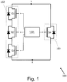
Fig. 1 is part schematic, part block diagram according to one or more illustrative embodiments. -
Fig. 2 is part schematic, part block diagram according to one or more illustrative embodiments. -
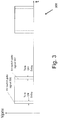
Fig. 3 is a timing diagram according to one or more illustrative embodiments. -
Fig. 4 is part schematic, part block diagram according to one or more illustrative embodiments. -
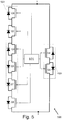
Fig. 5 is part schematic, part block diagram according to one or more illustrative embodiments. -
Fig. 6 is a block diagram according to one or more illustrative embodiments. - In the following description of various illustrative embodiments, reference is made to the accompanying drawings, which form a part hereof, and in which is shown, by way of illustration, various embodiments in which aspects of the disclosure may be practiced. It is to be understood that other embodiments may be utilized and structural and functional modifications may be made, without departing from the scope of the present disclosure.
- Reference is now made to
Fig. 1 , which illustrates a switch circuit according to illustrative embodiments.Switch circuit 100 may feature afirst leg 102 having switches Q1, Q2 and Q3 connected in series between terminals X and Y. Switches Q1-Q3 may be low-voltage MOSFETs (LVMs), for example, MOSFETs rated to block a drain-to-source voltage of about 100V (e.g. 50V, 80V, 100V, 120V, 150V, 200V, etc.). Switches Q1-Q3 may be stacked (i.e., serially connected) in a source-to-drain configuration, such that the body diodes of switches Q1-Q3 are oriented in the same direction (i.e., the anode of the parasitic diode of switch Q1 is connected to the cathode of the parasitic diode of switch Q2, and the anode of the parasitic diode of switch Q2 is connected to the cathode of the parasitic diode of switch Q3), to increase the voltage blocking capability offirst leg 102. For example, if each of switches Q1-Q3 is an 80V switch (i.e., is rated to withstand a voltage of 80V),first leg 102 may have an equivalent rating of 80*3=240V. - Stacking low-voltage switches to achieve a higher voltage rating may provide certain advantaged compared to using a single high-voltage switch. For example, three serially connected 100V MOSFETs may have a total conduction resistance (Rds,on) that may be significantly lower than the conduction resistance of a single 250V MOSFET. For example, a single 100V MOSFET may have Rds,on = 2mΩ, while a single 250V MOSFET may have Rds,on = 50mΩ. Since conduction losses are given by

- Serially connecting LVMs may present certain challenges when switching the LVMs between states. For example, switches Q1-Q3 are serially connected between terminals X and Y and in the OFF position, and it is desired to switch the switches to the ON state, timing the switching to be simultaneous may be challenging (e.g., because of manufacturing variations between the switches Q1-Q3 which may require three different gate-to-source voltages to drive the three switches to the ON state. Further, a controller may be configured to output three simultaneous control signals, and timing variation might reduce the effectiveness of the control signal. Additionally, timing variation between the control signals may result damage to one or more of the switches. For example, if switches Q1 and Q2 are switched to the ON state before switch Q3, the drain-to-source voltage across switch Q3 may be large (e.g., 200V, above switch Q3's voltage ratings) and may cause damage to switch Q3. Similarly, when switching switches Q1-Q3 from the ON state to the OFF state, timing and/or manufacturing variations may cause damage (e.g., due to avalanche breakdown) to one or more of switches Q1-Q3.
- A
second leg 103 may be connected in parallel tofirst leg 102.Second leg 103 may include a high-voltage switch or switches (e.g., a high-voltage MOSFET (HVM), or multiple parallel-connected HVMs which may increase a peak current rating of the second leg) Q4 rated to withstand a full voltage between nodes X and Y. For example,second leg 103 may be rated to withstand 600V. By switching the state of switch Q4 in tandem with switches Q1-Q3, the operational challenges of operating switches Q1-Q3 may be partially or fully alleviated. For example, when switching the state ofswitch circuit 100 from the OFF state to the ON state, switch Q4 may be switched to the ON state before switches Q1-Q3. By switching the state of switch Q4 before switches Q1-Q3, the voltage stress across switches Q1-Q3 may be significantly reduced (e.g., the voltage stress may be close to 0V), reducing the risk of timing variation causing damage to one of switches Q1-Q3. Furthermore, the switching of switches Q1-Q3 may induce low switching losses due to the low-voltage drop across switches Q1-Q3 during the switching (i.e., near Zero Voltage Switching). After switch Q4 and switches Q1-Q3 are switched ON, switch Q4 may be switched OFF (with switches Q1-Q3 providing a current path), or switch Q4 may remain ON, to provide an additional current path (though switch Q1-Q3 may provide the main current path due to the low Rds,on parameters of switches Q1-Q3). - In some embodiments, switch Q4 may be implemented using a wide gap band transistor, for example, a Silicon Carbide (SiC) or a Gallium Nitride (GaN) transistor. Using a wide gap band transistor may provide enhanced reverse recovery compared to a HV MOSFET.
- Switches Q1-Q4 may be controlled by a
controller 101.Controller 101 may be or include an analog controller, microprocessor, Digital Signal Processor (DSP), Application-Specific Integrated Circuit (ASIC), and/or a Field Programmable Gate Array (FPGA).Controller 101 may time the switching of switches Q1-Q4 to reduce switching and conduction losses during operation ofswitch circuit 100. - Reference is now made to
Fig. 2 , which illustrates a switch circuit according to illustrative embodiments.Switch circuit 200 may feature afirst leg 102 having switches Q1, Q2 and Q3 connected in series between terminals X and Y.First leg 102 may be the same asfirst leg 102 ofFig. 1 .Second leg 203 may include switch Q4 which may be the same as switch Q4 ofFig. 1 , and may further include diode D2 serially connected to switch Q4. Diode D2 may be oriented to prevent current from flowing through the body diode of switch Q4 (which may be desirable where the body diode is low-quality, i.e., lossy).Third leg 204 may include diode D1 disposed such that the cathode of diode D1 is connected (e.g., coupled) to node Y and the anode of diode D1 is connected (e.g., coupled) to node X. Diode D1 may be, for example, a silicon-carbide diode. Diode D1 may have a relatively low conduction voltage, to provide an efficient (e.g., having low-losses) current path between nodes X and Y and to reduce the reverse-recovery energy loss (when switching from ON to OFF) ofswitch circuit 200. - Reference is now made to
Fig. 3 , which illustrates a timing diagram for operating (e.g., via acontroller 101 ofFig. 1 ) a switch circuit, for example, switch circuits 100 (Fig. 1 ) or 200 (Fig. 2 ). Timing diagram 300 shows gate voltage signals which may be applied to switches Q1-Q4 ofFig. 1 orFig. 2 . Timing diagram 300 shows a HVswitch gate signal 301 and a LVswitch gate signal 302. The HV and LV switches may be operated as follows: - a. When switching from OFF to ON, The HV switch (e.g., Q4) may be turned ON, conducting current and reducing the voltage across the LV switches.
- b. After a suitably short delay, the LV switches may be turned on and short out the HV switch, providing a significantly lower conduction path for the main current. If the LV switches have an intrinsically larger switching delay than the HV switch, the controller operating the LV and HV switches might not insert any delay.
- c. After the required ON time, the LV switches may be turned off and the current may commutate back to the HV switch.
- d. Again after a suitable short delay, the HV switch may be switched off and its drain-source voltage may rise.
- Reference is now made to
Fig. 4 , which shows aswitch circuit 400 according to illustrative embodiments.Switch circuit 400 may comprise afirst leg 402, asecond leg 403 and athird leg 404.First leg 402 may include a series-connected group of LV switches Q1-Q3. Switches Q1 and Q2 may be oriented in a first direction, and switch Q3 may be oriented in a second direction (e.g., the anodes of switches Q2 and Q3 may be connected to a common node). Switch Q3 may be an a LV switch (e.g., having a voltage rating of 80V-120V) or an ultra-LV switch (e.g., may have a voltage rating of about 30V) and may be operated to improve commutation ofswitch circuit 400 by "forcing" current out of the body diodes of switches Q1 and Q2 when they are operating in rectification mode and into switch Q4 prior to turning switches Q4 and Q5 OFF. - In some embodiments, switch Q3 may be replaced with a diode (e.g., a Schottky diode) connected back-to-back with switch Q1 or with switch Q2, and the diode may similarly serve to prevent current from flowing through the body diodes of switches Q1 and Q2.
-
Second leg 403 may be connected in parallel tofirst leg 402 and may feature back-to-back (e.g., having connected anodes) HV switches Q4 and Q5. Switch Q5 may serve to block current from flowing through the body diode of switch Q4 (similarly to diode D2 ofFig. 2 ).Third leg 404 may be similar to or the same asthird leg 204 ofFig. 2 , and may comprise diode D1. -
First leg 402,second leg 403 andthird leg 404 may be controlled bycontroller 101, which may be the same as or similar tocontroller 101 of Fig. -
Third leg 404 might not be featured in certain embodiments. For example, where thesecond leg 403 features switches having reasonably high-quality body diodes (e.g., HV Gallium-Nitride (GaN) switches) and/or good reverse recovery characteristics (e.g., low reverse recovery losses). - Reference is now made to
Fig. 5 , which shows aswitch circuit 500 according to illustrative embodiments.Switch circuit 500 may be a bidirectional switch circuit, designed and operated to allow controlling current flow from node X to node Y and/or from node Y to node X.First leg 502 may include a first series-connected group of LV switches Q1-Q3 oriented in a first direction (e.g., having body diodes oriented to block current from flowing from node Y to node X) and a second series-connected group of LV switches Q6-Q8 oriented in a second direction (e.g., having body diodes oriented to block current from flowing from node X to node Y). By using two back-to-back groups of serially connected LV switches,first leg 502 may provide a high bidirectional voltage blocking capability between nodes X and Y and between nodes Y and X. - Second leg 503 may be connected in parallel to
first leg 502 and may feature back-to-back (e.g., having connected anodes) HV switches Q4 and Q5. HV switches are connected back-to-back to provide a high bidirectional voltage blocking capability between nodes X and Y and between nodes Y and X. - Reference is now made to
Fig. 6 , which shows an integrated switch circuit according to illustrative embodiments.Switch circuit 600 may be an integrated assembly (e.g., a PCB or a module) of switches Q1-Q4 ofFig. 1 . Nodes X and Y may be externally available via externals terminals, the gate terminals of switches Q1-Q3 may be available via the Leg1ON terminal, and the gate terminal of switch Q4 may be available via the Leg2ON terminal. Terminals Leg1ON and Leg2ON may be coupled to suitable controller (e.g., a controller similar to or the same ascontroller 101 ofFig. 1 ). In some embodiments, a controller may be further integrated inswitch circuit 600, with auxiliary power provided to the controller via auxiliary terminal Aux. Switches Q1-Q4 ofFig. 1 (along with other circuitry, for example, gate driver circuits) may be integrated using a single module package, or may be integrated as a fabrication structure (e.g., at a wafer level). Integrating components such as switches may provide lower cost, improved efficiency and increased ease-of-use. In some embodiments, an integrated controller may provide simpler control presented to a user. For example, the two terminals Leg1ON and Leg2ON may be unified to a single terminal for receiving simple logical ON/OFF command signals, and an internal controller may handle the timing configuration ofFig. 3 . - In embodiments involving additional switches (e.g., switch Q5 of
Fig. 4 ) or devices requiring control signals,switch circuit 600 may include additional terminals available for receiving control signals. - Embodiments disclosed herein employ switching legs having, for example, two or three MOSFETs connected in series. It is to be understood that other switches may be used instead of or in addition to MOSFETs, and any number of switches may be used. For example, eight 100V LVMs may be stacked to form an equivalent 800V switching leg connected in parallel to a leg having a 1200V IGBT. As another example, three 1200V IGBTs may be stacked to form an equivalent 3600V switching leg connected in parallel to a leg having a 3.3kV SiCFET.
- MOSFETs are used as examples of switches which come in low-voltage variants and high-voltage variants, and may be used to implement switches used to form switching circuits disclosed herein. Other types of switches may be used, such as bipolar junction transformers (BJTs), insulated gate bipolar transistors (IGBTs), gallium-nitride switches (GaNs), Silicon-Carbide switches (SiCs), and more.
- For example, power BJTs or LV IGBTs may be used as LV switches Q1-Q3 of
Fig. 1 . Switch Q4 may be a superjunction MOSFET, a SiC switch or a GaN switch. Diode D1 ofFig. 2 may be a Schottky diode (e.g., for use in a low-voltage application), a silicon diode, a SiC diode, or a GaN Schottky diode. - As another example, switches Q1-Q3 of
Fig. 1 may be thyristors, and switch Q4 may be an IGBT. In some embodiments, switches Q1-Q3 ofFig. 1 may be IGBTs and switch Q4 may be a SiC switch. - It is noted that various connections are set forth between elements herein. These connections are described in general and, unless specified otherwise, may be direct or indirect; this specification is not intended to be limiting in this respect. Further, elements of one embodiment may be combined with elements from other embodiments in appropriate combinations or subcombinations. For example, switch Q5 of
Fig. 4 may replace diode D2 ofFig. 2 . - According to a first illustrative embodiment, there is provided a switching device. The switching device includes a first leg comprising a plurality of transistors connected in series. The switching device also includes a second leg comprising a transistor, connected in parallel to the first leg. The switching device further includes a controller controlling the plurality of transistors of the first leg and the transistor of the second leg. The controller is configured to turn the switching device from a first state to a second state by first turning the transistor of the second leg from the first state to the second state and then turning the plurality of transistors of the first leg from the first state to the second state.
- For the switching device according to the first illustrative embodiment, the plurality of transistors of the first leg comprise at least two low-voltage MOSFETs.
- For the switching device according to the first illustrative embodiment, the transistor of the second leg comprises a high-voltage MOSFET.
- For the switching device according to the first illustrative embodiment, the at least two low-voltage MOSFETs have a rated maximum voltage of no more than 120V.
- For the switching device according to the first illustrative embodiment, the first state is an ON state and the second state is an OFF state.
- For the switching device according to the first illustrative embodiment, the first state is an OFF state and the second state is an ON state
- For the switching device according to the first illustrative embodiment, the switching device further includes a diode connected in series with the transistor to form the second leg.
- For the switching device according to the first illustrative embodiment, the switching device further includes a third leg coupled in parallel to the first leg and the second leg, the third leg comprising a diode.
- For the switching device according to the first illustrative embodiment, the second leg further includes a second transistor connected in series with the transistor of the second leg.
- For the switching device according to the first illustrative embodiment, the switching device further includes a third leg coupled in parallel to the first leg and the second leg, the third leg comprising a diode.
- According to a second illustrative embodiment, there is provided a method of forming a switching device. The method includes connecting a plurality of transistors in series to form a first leg. The method also includes connecting a second leg comprising a transistor in series to the first leg. The method further includes controlling the plurality of transistors of the first leg and the transistor of the second leg by turning the switching device from a first state to a second state by first turning the transistor of the second leg from the first state to the second state and then turning the plurality of transistors of the first leg from the first state to the second state.
- For the method according to the second illustrative embodiment, the plurality of transistors of the first leg comprise at least two low-voltage MOSFETs.
- For the method according to the second illustrative embodiment, the transistor of the second leg comprises a high-voltage MOSFET.
- For the method according to the second illustrative embodiment, the at least two low-voltage MOSFETs have a rated maximum voltage of no more than 120V.
- For the method according to the second illustrative embodiment, the first state is an ON state and the second state is an OFF state.
- For the method according to the second illustrative embodiment, the first state is an OFF state and the second state is an ON state.
- For the method according to the second illustrative embodiment, the method further includes connecting a diode connected in series with the transistor in the second leg.
- For the method according to the second illustrative embodiment, the method further includes connecting a second transistor connected in series with the transistor in the second leg.
- According to a third illustrative embodiment, there is provided a switching device. The switching device includes a first leg comprising a first plurality of transistors connected in series. The switching device further includes a second leg comprising a second plurality of transistors connected in series, the second leg connected in parallel to the first leg. The switching device also includes a controller controlling the first plurality of transistors of the first leg and the second plurality of transistors of the second leg. The controller is configured to turn the switching device from a first state to a second state by first turning the second plurality of transistors of the second leg from the first state to the second state and then turning the first plurality of transistors of the first leg from the first state to the second state.
- For the switching device according to the third illustrative embodiment, the first state is an OFF state and the second state is an ON state, or the first state is an ON state and the second state is an OFF state.
- Various characteristics of various embodiments of the invention as hereinafter highlighted in a set of numbered claims. These characteristics are not to be interpreted as being limiting on the invention or inventive concept, but are provided merely as a highlighting of some characteristics of the invention as described in the description without suggesting a particular order of importance or relevancy of such characteristics.
- Clause 1: A switching device comprising:
- a first leg comprising a plurality of transistors connected in series,
- a second leg comprising a transistor, connected in parallel to the first leg,
- a controller controlling the plurality of transistors of the first leg and the transistor of the second leg,
- wherein the controller is configured to turn the switching device from a first state to a second state by first turning the transistor of the second leg from the first state to the second state and then turning the plurality of transistors of the first leg from the first state to the second state.
- Clause 2: The switching device of clause 1, wherein the plurality of transistors of the first leg comprise at least two low-voltage MOSFETs.
- Clause 3: The switching device of clause 1 or 2, wherein the transistor of the second leg comprises a high-voltage MOSFET.
- Clause 4: The switching device of any of clauses 1-3, wherein the at least two low-voltage MOSFETs have a rated maximum voltage of no more than 120V.
- Clause 5: The switching device of any of clauses 1-4, wherein the first state is an ON state and the second state is an OFF state.
- Clause 6: The switching device of any of clauses 1-4, wherein the first state is an OFF state and the second state is an ON state.
- Clause 7: The switching device of any of the preceding clauses, further comprising a diode connected in series with the transistor to form the second leg.
- Clause 8: The switching device of any of the preceding clauses, further comprising a third leg coupled in parallel to the first leg and the second leg, the third leg comprising a diode.
- Clause 9: The switching device of any of the preceding clauses, wherein the second leg further comprises a second transistor connected in series with the transistor of the second leg.
- Clause 10: The switching device of clause 9, further comprising a third leg coupled in parallel to the first leg and the second leg, the third leg comprising a diode.
- Clause 11: A method of forming a switching device, comprising:
- connecting a plurality of transistors in series to form a first leg,
- connecting a second leg comprising a transistor in series to the first leg,
- controlling the plurality of transistors of the first leg and the transistor of the second leg by:
turning the switching device from a first state to a second state by first turning the transistor of the second leg from the first state to the second state and then turning the plurality of transistors of the first leg from the first state to the second state.
- Clause 12: The method of clause 11, wherein the plurality of transistors of the first leg comprise at least two low-voltage MOSFETs.
- Clause 13: The method of clause 11 or 12, wherein the transistor of the second leg comprises a high-voltage MOSFET.
- Clause 14: The method of any of clauses 11-13, wherein the at least two low-voltage MOSFETs have a rated maximum voltage of no more than 120V.
- Clause 15: The method of any of clauses 11-14, wherein the first state is an ON state and the second state is an OFF state.
- Clause 16: The method of any of clauses 11-14, wherein the first state is an OFF state and the second state is an ON state.
- Clause 17: The method of any of clauses 11-16, further comprising:
connecting a diode connected in series with the transistor in the second leg. - Clause 18: The method of any of clauses 11-17, further comprising:
connecting a second transistor connected in series with the transistor in the second leg. - Clause 19: A switching device comprising:
- a first leg comprising a first plurality of transistors connected in series,
- a second leg comprising a second plurality of transistors connected in series, the second leg connected in parallel to the first leg,
- a controller controlling the first plurality of transistors of the first leg and the second plurality of transistors of the second leg,
- wherein the controller is configured to turn the switching device from a first state to a second state by first turning the second plurality of transistors of the second leg from the first state to the second state and then turning the first plurality of transistors of the first leg from the first state to the second state.
- Clause 20: The switching device of clause 19, wherein the first state is an OFF state and the second state is an ON state, or the first state is an ON state and the second state is an OFF state.
Claims (15)
- A switching device comprising:a first leg comprising a plurality of transistors connected in series,a second leg comprising a transistor, connected in parallel to the first leg,a controller controlling the plurality of transistors of the first leg and the transistor of the second leg,wherein the controller is configured to turn the switching device from a first state to a second state by first turning the transistor of the second leg from the first state to the second state and then turning the plurality of transistors of the first leg from the first state to the second state.
- The switching device of claim 1, wherein the plurality of transistors of the first leg comprise at least two low-voltage MOSFETs.
- The switching device of claim 2, wherein the transistor of the second leg comprises a high-voltage MOSFET.
- The switching device of claim 3, wherein the at least two low-voltage MOSFETs have a rated maximum voltage of no more than 120V.
- The switching device of claim 1, wherein the first state is an ON state and the second state is an OFF state.
- The switching device of claim 1, wherein the first state is an OFF state and the second state is an ON state.
- The switching device of claim 3, further comprising a diode connected in series with the transistor to form the second leg.
- The switching device of claim 1, wherein the second leg further comprises a second transistor connected in series with the transistor of the second leg.
- The switching device of claim 8, further comprising a third leg coupled in parallel to the first leg and the second leg, the third leg comprising a diode
- A method of forming a switching device, comprising:connecting a plurality of transistors in series to form a first leg,connecting a second leg comprising a transistor in series to the first leg,controlling the plurality of transistors of the first leg and the transistor of the second leg by:
turning the switching device from a first state to a second state by first turning the transistor of the second leg from the first state to the second state and then turning the plurality of transistors of the first leg from the first state to the second state. - The method of claim 10, wherein the plurality of transistors of the first leg comprise at least two low-voltage MOSFETs.
- The method of claim 11, wherein the transistor of the second leg comprises a high-voltage MOSFET, and wherein the at least two low-voltage MOSFETs have a rated maximum voltage of no more than 120V.
- The method of any claims 10-12, wherein the first state is an ON state and the second state is an OFF state, or the first state is an OFF state and the second state is an ON state.
- The method of any of claims 10-13, further comprising:
connecting a diode connected in series with the transistor of the second leg. - The method of any of claims 10-14, further comprising:
connecting a second transistor connected in series with the transistor of the second leg.
Applications Claiming Priority (1)
| Application Number | Priority Date | Filing Date | Title |
|---|---|---|---|
| US201762510838P | 2017-05-25 | 2017-05-25 |
Publications (1)
| Publication Number | Publication Date |
|---|---|
| EP3407494A1 true EP3407494A1 (en) | 2018-11-28 |
Family
ID=62244408
Family Applications (1)
| Application Number | Title | Priority Date | Filing Date |
|---|---|---|---|
| EP18174053.1A Withdrawn EP3407494A1 (en) | 2017-05-25 | 2018-05-24 | Efficient switching circuit |
Country Status (3)
| Country | Link |
|---|---|
| US (5) | US10608624B2 (en) |
| EP (1) | EP3407494A1 (en) |
| CN (2) | CN108964458B (en) |
Families Citing this family (3)
| Publication number | Priority date | Publication date | Assignee | Title |
|---|---|---|---|---|
| US10608624B2 (en) * | 2017-05-25 | 2020-03-31 | Solaredge Technologies Ltd. | Efficient switching circuit |
| WO2019176077A1 (en) * | 2018-03-16 | 2019-09-19 | 新電元工業株式会社 | Semiconductor switch control circuit and switching power supply device |
| US12255550B2 (en) * | 2021-03-12 | 2025-03-18 | Wisconsin Alumni Research Foundation | Current source inverter using bidirectional switches with bidirectional power flow capability |
Citations (5)
| Publication number | Priority date | Publication date | Assignee | Title |
|---|---|---|---|---|
| US6249111B1 (en) * | 2000-06-22 | 2001-06-19 | Intel Corporation | Dual drive buck regulator |
| US20030038615A1 (en) * | 2001-08-23 | 2003-02-27 | Fairchild Semiconductor Corporation | Method and circuit for reducing losses in DC-DC converters |
| US7391133B1 (en) * | 2002-09-28 | 2008-06-24 | Hennessy Michael J | Hybrid switch |
| US20110273219A1 (en) * | 2010-05-06 | 2011-11-10 | Micron Technology, Inc. | Voltage switching in a memory device |
| US20120057387A1 (en) * | 2010-08-10 | 2012-03-08 | Jih-Sheng Lai | Hybrid switch for resonant power converters |
Family Cites Families (44)
| Publication number | Priority date | Publication date | Assignee | Title |
|---|---|---|---|---|
| US4178605A (en) * | 1978-01-30 | 1979-12-11 | Rca Corp. | Complementary MOS inverter structure |
| US5155289A (en) * | 1991-07-01 | 1992-10-13 | General Atomics | High-voltage solid-state switching devices |
| US5401987A (en) * | 1993-12-01 | 1995-03-28 | Imp, Inc. | Self-cascoding CMOS device |
| US6118324A (en) * | 1997-06-30 | 2000-09-12 | Xilinx, Inc. | Output driver with reduced ground bounce |
| US6111390A (en) * | 1998-01-20 | 2000-08-29 | Kokusan Kenki Co., Ltd. | Magneto-equipped power device |
| JP3166840B2 (en) * | 1998-03-10 | 2001-05-14 | 日本電気株式会社 | Waveform output circuit and device having the same |
| US7230470B1 (en) * | 2001-03-02 | 2007-06-12 | Volterra Semiconductor Corporation | Power switch using a field-effect transistor (FET) pair |
| US7071763B2 (en) * | 2002-12-27 | 2006-07-04 | Emosyn America, Inc. | Transistor circuits for switching high voltages and currents without causing snapback or breakdown |
| ITRM20030085A1 (en) * | 2003-02-27 | 2004-08-28 | Micron Technology Inc | VARIABLE IMPEDANCE OUTPUT BUFFER. |
| TWI288478B (en) * | 2004-08-26 | 2007-10-11 | Realtek Semiconductor Corp | High voltage tolerance output stage |
| US7537970B2 (en) * | 2006-03-06 | 2009-05-26 | Semiconductor Components Industries, L.L.C. | Bi-directional transistor with by-pass path and method therefor |
| KR101154894B1 (en) * | 2007-08-21 | 2012-06-18 | 삼성전자주식회사 | Switching power source apparatus and control method thereof |
| CN101971477B (en) * | 2008-01-21 | 2014-07-23 | Abb技术有限公司 | Voltage source converter and its control method |
| US7741883B2 (en) | 2008-05-21 | 2010-06-22 | Honeywell International Inc. | Method of switching and switching device for solid state power controller applications |
| US8084783B2 (en) * | 2008-11-10 | 2011-12-27 | International Rectifier Corporation | GaN-based device cascoded with an integrated FET/Schottky diode device |
| US9035625B2 (en) * | 2009-12-23 | 2015-05-19 | R2 Semiconductor | Common cascode routing bus for high-efficiency DC-to-DC conversion |
| JP5574845B2 (en) * | 2010-06-22 | 2014-08-20 | 株式会社東芝 | Power converter |
| BR112012032391A2 (en) * | 2010-07-01 | 2016-11-08 | Mitsubishi Electric Corp | power semiconductor module |
| US20120126317A1 (en) * | 2010-11-18 | 2012-05-24 | Alpha And Omega Semiconductor Incorporated | Accufet with integrated clamping circuit |
| CN102647099A (en) * | 2011-02-22 | 2012-08-22 | 艾默生网络能源系统北美公司 | A combined switch and synchronous rectification circuit |
| JP2012227680A (en) * | 2011-04-19 | 2012-11-15 | Fujitsu Semiconductor Ltd | Switching circuit device and power supply device having the same |
| WO2013018282A1 (en) * | 2011-07-29 | 2013-02-07 | 三洋電機株式会社 | Switching apparatus, and photovoltaic power generation system and vehicle drive system using same |
| US9030054B2 (en) * | 2012-03-27 | 2015-05-12 | Raytheon Company | Adaptive gate drive control method and circuit for composite power switch |
| DE102013010188A1 (en) * | 2012-06-21 | 2013-12-24 | Fairchild Semiconductor Corp. | Switching circuit and control circuit |
| KR20140000010A (en) * | 2012-06-22 | 2014-01-02 | 삼성전자주식회사 | Semiconductor memory device |
| US9571086B1 (en) * | 2012-12-05 | 2017-02-14 | Lockheed Martin Corporation | Bi-directional switch |
| CN105164598B (en) * | 2013-03-15 | 2017-09-12 | 沃尔泰拉半导体公司 | Voltage regulator with multiple transistors |
| JP2016136793A (en) * | 2013-05-14 | 2016-07-28 | シャープ株式会社 | Switching power supply device and inverter, converter, and solar power controller using the same |
| JPWO2015079762A1 (en) * | 2013-11-29 | 2017-03-16 | シャープ株式会社 | Rectifier |
| TWI509972B (en) * | 2014-06-25 | 2015-11-21 | Delta Electronics Inc | Soft-switching bi-directional power converter and method of operating the same |
| US9722581B2 (en) * | 2014-07-24 | 2017-08-01 | Eaton Corporation | Methods and systems for operating hybrid power devices using driver circuits that perform indirect instantaneous load current sensing |
| US9748224B2 (en) * | 2014-10-28 | 2017-08-29 | Semiconductor Components Industries, Llc | Heterojunction semiconductor device having integrated clamping device |
| US10050620B2 (en) * | 2015-02-27 | 2018-08-14 | Renesas Electronics America Inc. | Cascode connected SiC-JFET with SiC-SBD and enhancement device |
| US9484897B2 (en) * | 2015-03-18 | 2016-11-01 | Peregrine Semiconductor Corporation | Level shifter |
| JP2017055255A (en) * | 2015-09-09 | 2017-03-16 | 株式会社東芝 | Power semiconductor device |
| JP6388039B2 (en) * | 2015-11-17 | 2018-09-12 | 株式会社オートネットワーク技術研究所 | Switch circuit and power supply system |
| GB201522651D0 (en) * | 2015-12-22 | 2016-02-03 | Rolls Royce Controls & Data Services Ltd | Solid state power control |
| CN105553318B (en) * | 2015-12-23 | 2020-04-21 | 华为技术有限公司 | An Equivalent Transistor and Three-Level Inverter |
| US10411694B2 (en) * | 2016-07-22 | 2019-09-10 | Abb Schweiz Ag | Solid state switch system |
| JP6722101B2 (en) * | 2016-12-27 | 2020-07-15 | ルネサスエレクトロニクス株式会社 | Semiconductor device and overcurrent protection device |
| US10230364B2 (en) * | 2017-04-26 | 2019-03-12 | Futurewei Technologies, Inc. | Hybrid power devices |
| US10608624B2 (en) * | 2017-05-25 | 2020-03-31 | Solaredge Technologies Ltd. | Efficient switching circuit |
| US10536094B2 (en) * | 2017-11-20 | 2020-01-14 | Solaredge Technologies Ltd. | Efficient switching for converter circuit |
| EP4235786A1 (en) * | 2022-02-28 | 2023-08-30 | Infineon Technologies AG | Semiconductor switching module with insulated gate bipolar transistor and unipolar switching device |
-
2018
- 2018-05-21 US US15/984,516 patent/US10608624B2/en active Active
- 2018-05-21 CN CN201810491782.1A patent/CN108964458B/en not_active Expired - Fee Related
- 2018-05-21 CN CN202310347641.3A patent/CN116545259A/en active Pending
- 2018-05-24 EP EP18174053.1A patent/EP3407494A1/en not_active Withdrawn
-
2020
- 2020-02-20 US US16/795,653 patent/US11374562B2/en active Active
-
2022
- 2022-05-18 US US17/747,114 patent/US11695402B2/en active Active
-
2023
- 2023-05-12 US US18/316,358 patent/US12166475B2/en active Active
-
2024
- 2024-11-05 US US18/937,120 patent/US20250062759A1/en active Pending
Patent Citations (5)
| Publication number | Priority date | Publication date | Assignee | Title |
|---|---|---|---|---|
| US6249111B1 (en) * | 2000-06-22 | 2001-06-19 | Intel Corporation | Dual drive buck regulator |
| US20030038615A1 (en) * | 2001-08-23 | 2003-02-27 | Fairchild Semiconductor Corporation | Method and circuit for reducing losses in DC-DC converters |
| US7391133B1 (en) * | 2002-09-28 | 2008-06-24 | Hennessy Michael J | Hybrid switch |
| US20110273219A1 (en) * | 2010-05-06 | 2011-11-10 | Micron Technology, Inc. | Voltage switching in a memory device |
| US20120057387A1 (en) * | 2010-08-10 | 2012-03-08 | Jih-Sheng Lai | Hybrid switch for resonant power converters |
Also Published As
| Publication number | Publication date |
|---|---|
| US20180343002A1 (en) | 2018-11-29 |
| US11374562B2 (en) | 2022-06-28 |
| US11695402B2 (en) | 2023-07-04 |
| CN116545259A (en) | 2023-08-04 |
| US20220345124A1 (en) | 2022-10-27 |
| US12166475B2 (en) | 2024-12-10 |
| US10608624B2 (en) | 2020-03-31 |
| US20230336169A1 (en) | 2023-10-19 |
| US20200259486A1 (en) | 2020-08-13 |
| CN108964458A (en) | 2018-12-07 |
| US20250062759A1 (en) | 2025-02-20 |
| CN108964458B (en) | 2023-04-21 |
Similar Documents
| Publication | Publication Date | Title |
|---|---|---|
| JP6705936B2 (en) | Method and circuit for operating a circuit | |
| US9472549B2 (en) | Cascoded semiconductor devices | |
| US12166475B2 (en) | Efficient switching circuit | |
| EP3243276B1 (en) | High voltage switch | |
| Zhang et al. | Evaluation of 600 V cascode GaN HEMT in device characterization and all-GaN-based LLC resonant converter | |
| EP2816729A1 (en) | Depletion mode group III-V transistor with high voltage group IV enable switch | |
| CN102684661B (en) | There is the circuit arrangement of MOSFET and IGBT | |
| CN106464242A (en) | Cascode switching circuit | |
| KR20160122663A (en) | Paralleling power switches using a differential mode choke in the gate drive loop | |
| Green et al. | Gate drive for power MOSFETs in switching applications | |
| WO2016000840A1 (en) | Power semiconductor module | |
| EP3834275B1 (en) | Performance enhancement of silicon-based device | |
| EP3057232A1 (en) | Circuit breaker device | |
| JP7242487B2 (en) | semiconductor equipment | |
| US20250120173A1 (en) | Cascode Semiconductor Devices | |
| US10468971B2 (en) | Power converter configured for limiting switching overvoltage | |
| EP4668583A1 (en) | A bidirectional switching assembly | |
| US8767426B2 (en) | Matrix converter controlling apparatus |
Legal Events
| Date | Code | Title | Description |
|---|---|---|---|
| PUAI | Public reference made under article 153(3) epc to a published international application that has entered the european phase |
Free format text: ORIGINAL CODE: 0009012 |
|
| STAA | Information on the status of an ep patent application or granted ep patent |
Free format text: STATUS: THE APPLICATION HAS BEEN PUBLISHED |
|
| AK | Designated contracting states |
Kind code of ref document: A1 Designated state(s): AL AT BE BG CH CY CZ DE DK EE ES FI FR GB GR HR HU IE IS IT LI LT LU LV MC MK MT NL NO PL PT RO RS SE SI SK SM TR |
|
| AX | Request for extension of the european patent |
Extension state: BA ME |
|
| STAA | Information on the status of an ep patent application or granted ep patent |
Free format text: STATUS: REQUEST FOR EXAMINATION WAS MADE |
|
| 17P | Request for examination filed |
Effective date: 20190528 |
|
| RBV | Designated contracting states (corrected) |
Designated state(s): AL AT BE BG CH CY CZ DE DK EE ES FI FR GB GR HR HU IE IS IT LI LT LU LV MC MK MT NL NO PL PT RO RS SE SI SK SM TR |
|
| STAA | Information on the status of an ep patent application or granted ep patent |
Free format text: STATUS: EXAMINATION IS IN PROGRESS |
|
| 17Q | First examination report despatched |
Effective date: 20210601 |
|
| P01 | Opt-out of the competence of the unified patent court (upc) registered |
Effective date: 20230505 |
|
| GRAP | Despatch of communication of intention to grant a patent |
Free format text: ORIGINAL CODE: EPIDOSNIGR1 |
|
| STAA | Information on the status of an ep patent application or granted ep patent |
Free format text: STATUS: GRANT OF PATENT IS INTENDED |
|
| RIC1 | Information provided on ipc code assigned before grant |
Ipc: H03K 17/10 20060101AFI20251014BHEP Ipc: H03K 17/06 20060101ALI20251014BHEP Ipc: H03K 17/16 20060101ALI20251014BHEP Ipc: H03K 17/567 20060101ALN20251014BHEP Ipc: H03K 17/687 20060101ALN20251014BHEP Ipc: H03K 17/12 20060101ALN20251014BHEP |
|
| RIC1 | Information provided on ipc code assigned before grant |
Ipc: H03K 17/10 20060101AFI20251103BHEP Ipc: H03K 17/06 20060101ALI20251103BHEP Ipc: H03K 17/16 20060101ALI20251103BHEP Ipc: H03K 17/567 20060101ALN20251103BHEP Ipc: H03K 17/687 20060101ALN20251103BHEP Ipc: H03K 17/12 20060101ALN20251103BHEP |
|
| INTG | Intention to grant announced |
Effective date: 20251114 |
|
| STAA | Information on the status of an ep patent application or granted ep patent |
Free format text: STATUS: THE APPLICATION IS DEEMED TO BE WITHDRAWN |
|
| 18D | Application deemed to be withdrawn |
Effective date: 20260317 |