EP3407380A1 - Bonded body, power module substrate, bonded body manufacturing method, and power module substrate manufacturing method - Google Patents
Bonded body, power module substrate, bonded body manufacturing method, and power module substrate manufacturing method Download PDFInfo
- Publication number
- EP3407380A1 EP3407380A1 EP17741518.9A EP17741518A EP3407380A1 EP 3407380 A1 EP3407380 A1 EP 3407380A1 EP 17741518 A EP17741518 A EP 17741518A EP 3407380 A1 EP3407380 A1 EP 3407380A1
- Authority
- EP
- European Patent Office
- Prior art keywords
- layer
- intermetallic compound
- equal
- ceramic substrate
- compound layer
- Prior art date
- Legal status (The legal status is an assumption and is not a legal conclusion. Google has not performed a legal analysis and makes no representation as to the accuracy of the status listed.)
- Granted
Links
Images




Classifications
-
- H—ELECTRICITY
- H10—SEMICONDUCTOR DEVICES; ELECTRIC SOLID-STATE DEVICES NOT OTHERWISE PROVIDED FOR
- H10W—GENERIC PACKAGES, INTERCONNECTIONS, CONNECTORS OR OTHER CONSTRUCTIONAL DETAILS OF DEVICES COVERED BY CLASS H10
- H10W20/00—Interconnections in chips, wafers or substrates
- H10W20/40—Interconnections external to wafers or substrates, e.g. back-end-of-line [BEOL] metallisations or vias connecting to gate electrodes
- H10W20/41—Interconnections external to wafers or substrates, e.g. back-end-of-line [BEOL] metallisations or vias connecting to gate electrodes characterised by their conductive parts
- H10W20/44—Conductive materials thereof
- H10W20/4403—Conductive materials thereof based on metals, e.g. alloys, metal silicides
- H10W20/4421—Conductive materials thereof based on metals, e.g. alloys, metal silicides the principal metal being copper
-
- H—ELECTRICITY
- H10—SEMICONDUCTOR DEVICES; ELECTRIC SOLID-STATE DEVICES NOT OTHERWISE PROVIDED FOR
- H10W—GENERIC PACKAGES, INTERCONNECTIONS, CONNECTORS OR OTHER CONSTRUCTIONAL DETAILS OF DEVICES COVERED BY CLASS H10
- H10W40/00—Arrangements for thermal protection or thermal control
- H10W40/20—Arrangements for cooling
- H10W40/25—Arrangements for cooling characterised by their materials
- H10W40/255—Arrangements for cooling characterised by their materials having a laminate or multilayered structure, e.g. direct bond copper [DBC] ceramic substrates
-
- C—CHEMISTRY; METALLURGY
- C04—CEMENTS; CONCRETE; ARTIFICIAL STONE; CERAMICS; REFRACTORIES
- C04B—LIME, MAGNESIA; SLAG; CEMENTS; COMPOSITIONS THEREOF, e.g. MORTARS, CONCRETE OR LIKE BUILDING MATERIALS; ARTIFICIAL STONE; CERAMICS; REFRACTORIES; TREATMENT OF NATURAL STONE
- C04B35/00—Shaped ceramic products characterised by their composition; Ceramics compositions; Processing powders of inorganic compounds preparatory to the manufacturing of ceramic products
- C04B35/622—Forming processes; Processing powders of inorganic compounds preparatory to the manufacturing of ceramic products
- C04B35/64—Burning or sintering processes
- C04B35/645—Pressure sintering
-
- C—CHEMISTRY; METALLURGY
- C04—CEMENTS; CONCRETE; ARTIFICIAL STONE; CERAMICS; REFRACTORIES
- C04B—LIME, MAGNESIA; SLAG; CEMENTS; COMPOSITIONS THEREOF, e.g. MORTARS, CONCRETE OR LIKE BUILDING MATERIALS; ARTIFICIAL STONE; CERAMICS; REFRACTORIES; TREATMENT OF NATURAL STONE
- C04B37/00—Joining burned ceramic articles with other burned ceramic articles or other articles by heating
- C04B37/02—Joining burned ceramic articles with other burned ceramic articles or other articles by heating with metallic articles
- C04B37/023—Joining burned ceramic articles with other burned ceramic articles or other articles by heating with metallic articles characterised by the interlayer used
- C04B37/026—Joining burned ceramic articles with other burned ceramic articles or other articles by heating with metallic articles characterised by the interlayer used consisting of metals or metal salts
-
- C—CHEMISTRY; METALLURGY
- C22—METALLURGY; FERROUS OR NON-FERROUS ALLOYS; TREATMENT OF ALLOYS OR NON-FERROUS METALS
- C22C—ALLOYS
- C22C9/00—Alloys based on copper
- C22C9/02—Alloys based on copper with tin as the next major constituent
-
- H—ELECTRICITY
- H10—SEMICONDUCTOR DEVICES; ELECTRIC SOLID-STATE DEVICES NOT OTHERWISE PROVIDED FOR
- H10W—GENERIC PACKAGES, INTERCONNECTIONS, CONNECTORS OR OTHER CONSTRUCTIONAL DETAILS OF DEVICES COVERED BY CLASS H10
- H10W40/00—Arrangements for thermal protection or thermal control
- H10W40/01—Manufacture or treatment
- H10W40/03—Manufacture or treatment of arrangements for cooling
- H10W40/037—Assembling together parts thereof
-
- H—ELECTRICITY
- H10—SEMICONDUCTOR DEVICES; ELECTRIC SOLID-STATE DEVICES NOT OTHERWISE PROVIDED FOR
- H10W—GENERIC PACKAGES, INTERCONNECTIONS, CONNECTORS OR OTHER CONSTRUCTIONAL DETAILS OF DEVICES COVERED BY CLASS H10
- H10W40/00—Arrangements for thermal protection or thermal control
- H10W40/20—Arrangements for cooling
- H10W40/25—Arrangements for cooling characterised by their materials
- H10W40/258—Metallic materials
-
- H—ELECTRICITY
- H10—SEMICONDUCTOR DEVICES; ELECTRIC SOLID-STATE DEVICES NOT OTHERWISE PROVIDED FOR
- H10W—GENERIC PACKAGES, INTERCONNECTIONS, CONNECTORS OR OTHER CONSTRUCTIONAL DETAILS OF DEVICES COVERED BY CLASS H10
- H10W40/00—Arrangements for thermal protection or thermal control
- H10W40/20—Arrangements for cooling
- H10W40/25—Arrangements for cooling characterised by their materials
- H10W40/259—Ceramics or glasses
-
- H—ELECTRICITY
- H10—SEMICONDUCTOR DEVICES; ELECTRIC SOLID-STATE DEVICES NOT OTHERWISE PROVIDED FOR
- H10W—GENERIC PACKAGES, INTERCONNECTIONS, CONNECTORS OR OTHER CONSTRUCTIONAL DETAILS OF DEVICES COVERED BY CLASS H10
- H10W70/00—Package substrates; Interposers; Redistribution layers [RDL]
- H10W70/60—Insulating or insulated package substrates; Interposers; Redistribution layers
- H10W70/67—Insulating or insulated package substrates; Interposers; Redistribution layers characterised by their insulating layers or insulating parts
- H10W70/68—Shapes or dispositions thereof
- H10W70/6875—Shapes or dispositions thereof being on a metallic substrate, e.g. insulated metal substrates [IMS]
-
- H—ELECTRICITY
- H10—SEMICONDUCTOR DEVICES; ELECTRIC SOLID-STATE DEVICES NOT OTHERWISE PROVIDED FOR
- H10W—GENERIC PACKAGES, INTERCONNECTIONS, CONNECTORS OR OTHER CONSTRUCTIONAL DETAILS OF DEVICES COVERED BY CLASS H10
- H10W70/00—Package substrates; Interposers; Redistribution layers [RDL]
- H10W70/60—Insulating or insulated package substrates; Interposers; Redistribution layers
- H10W70/67—Insulating or insulated package substrates; Interposers; Redistribution layers characterised by their insulating layers or insulating parts
- H10W70/69—Insulating materials thereof
- H10W70/692—Ceramics or glasses
-
- C—CHEMISTRY; METALLURGY
- C04—CEMENTS; CONCRETE; ARTIFICIAL STONE; CERAMICS; REFRACTORIES
- C04B—LIME, MAGNESIA; SLAG; CEMENTS; COMPOSITIONS THEREOF, e.g. MORTARS, CONCRETE OR LIKE BUILDING MATERIALS; ARTIFICIAL STONE; CERAMICS; REFRACTORIES; TREATMENT OF NATURAL STONE
- C04B2235/00—Aspects relating to ceramic starting mixtures or sintered ceramic products
- C04B2235/65—Aspects relating to heat treatments of ceramic bodies such as green ceramics or pre-sintered ceramics, e.g. burning, sintering or melting processes
- C04B2235/656—Aspects relating to heat treatments of ceramic bodies such as green ceramics or pre-sintered ceramics, e.g. burning, sintering or melting processes characterised by specific heating conditions during heat treatment
- C04B2235/6562—Heating rate
-
- C—CHEMISTRY; METALLURGY
- C04—CEMENTS; CONCRETE; ARTIFICIAL STONE; CERAMICS; REFRACTORIES
- C04B—LIME, MAGNESIA; SLAG; CEMENTS; COMPOSITIONS THEREOF, e.g. MORTARS, CONCRETE OR LIKE BUILDING MATERIALS; ARTIFICIAL STONE; CERAMICS; REFRACTORIES; TREATMENT OF NATURAL STONE
- C04B2235/00—Aspects relating to ceramic starting mixtures or sintered ceramic products
- C04B2235/65—Aspects relating to heat treatments of ceramic bodies such as green ceramics or pre-sintered ceramics, e.g. burning, sintering or melting processes
- C04B2235/656—Aspects relating to heat treatments of ceramic bodies such as green ceramics or pre-sintered ceramics, e.g. burning, sintering or melting processes characterised by specific heating conditions during heat treatment
- C04B2235/6567—Treatment time
-
- C—CHEMISTRY; METALLURGY
- C04—CEMENTS; CONCRETE; ARTIFICIAL STONE; CERAMICS; REFRACTORIES
- C04B—LIME, MAGNESIA; SLAG; CEMENTS; COMPOSITIONS THEREOF, e.g. MORTARS, CONCRETE OR LIKE BUILDING MATERIALS; ARTIFICIAL STONE; CERAMICS; REFRACTORIES; TREATMENT OF NATURAL STONE
- C04B2235/00—Aspects relating to ceramic starting mixtures or sintered ceramic products
- C04B2235/65—Aspects relating to heat treatments of ceramic bodies such as green ceramics or pre-sintered ceramics, e.g. burning, sintering or melting processes
- C04B2235/658—Atmosphere during thermal treatment
- C04B2235/6581—Total pressure below 1 atmosphere, e.g. vacuum
-
- C—CHEMISTRY; METALLURGY
- C04—CEMENTS; CONCRETE; ARTIFICIAL STONE; CERAMICS; REFRACTORIES
- C04B—LIME, MAGNESIA; SLAG; CEMENTS; COMPOSITIONS THEREOF, e.g. MORTARS, CONCRETE OR LIKE BUILDING MATERIALS; ARTIFICIAL STONE; CERAMICS; REFRACTORIES; TREATMENT OF NATURAL STONE
- C04B2235/00—Aspects relating to ceramic starting mixtures or sintered ceramic products
- C04B2235/65—Aspects relating to heat treatments of ceramic bodies such as green ceramics or pre-sintered ceramics, e.g. burning, sintering or melting processes
- C04B2235/66—Specific sintering techniques, e.g. centrifugal sintering
- C04B2235/661—Multi-step sintering
-
- C—CHEMISTRY; METALLURGY
- C04—CEMENTS; CONCRETE; ARTIFICIAL STONE; CERAMICS; REFRACTORIES
- C04B—LIME, MAGNESIA; SLAG; CEMENTS; COMPOSITIONS THEREOF, e.g. MORTARS, CONCRETE OR LIKE BUILDING MATERIALS; ARTIFICIAL STONE; CERAMICS; REFRACTORIES; TREATMENT OF NATURAL STONE
- C04B2237/00—Aspects relating to ceramic laminates or to joining of ceramic articles with other articles by heating
- C04B2237/02—Aspects relating to interlayers, e.g. used to join ceramic articles with other articles by heating
- C04B2237/12—Metallic interlayers
- C04B2237/122—Metallic interlayers based on refractory metals
-
- C—CHEMISTRY; METALLURGY
- C04—CEMENTS; CONCRETE; ARTIFICIAL STONE; CERAMICS; REFRACTORIES
- C04B—LIME, MAGNESIA; SLAG; CEMENTS; COMPOSITIONS THEREOF, e.g. MORTARS, CONCRETE OR LIKE BUILDING MATERIALS; ARTIFICIAL STONE; CERAMICS; REFRACTORIES; TREATMENT OF NATURAL STONE
- C04B2237/00—Aspects relating to ceramic laminates or to joining of ceramic articles with other articles by heating
- C04B2237/02—Aspects relating to interlayers, e.g. used to join ceramic articles with other articles by heating
- C04B2237/12—Metallic interlayers
- C04B2237/124—Metallic interlayers based on copper
-
- C—CHEMISTRY; METALLURGY
- C04—CEMENTS; CONCRETE; ARTIFICIAL STONE; CERAMICS; REFRACTORIES
- C04B—LIME, MAGNESIA; SLAG; CEMENTS; COMPOSITIONS THEREOF, e.g. MORTARS, CONCRETE OR LIKE BUILDING MATERIALS; ARTIFICIAL STONE; CERAMICS; REFRACTORIES; TREATMENT OF NATURAL STONE
- C04B2237/00—Aspects relating to ceramic laminates or to joining of ceramic articles with other articles by heating
- C04B2237/02—Aspects relating to interlayers, e.g. used to join ceramic articles with other articles by heating
- C04B2237/12—Metallic interlayers
- C04B2237/126—Metallic interlayers wherein the active component for bonding is not the largest fraction of the interlayer
-
- C—CHEMISTRY; METALLURGY
- C04—CEMENTS; CONCRETE; ARTIFICIAL STONE; CERAMICS; REFRACTORIES
- C04B—LIME, MAGNESIA; SLAG; CEMENTS; COMPOSITIONS THEREOF, e.g. MORTARS, CONCRETE OR LIKE BUILDING MATERIALS; ARTIFICIAL STONE; CERAMICS; REFRACTORIES; TREATMENT OF NATURAL STONE
- C04B2237/00—Aspects relating to ceramic laminates or to joining of ceramic articles with other articles by heating
- C04B2237/30—Composition of layers of ceramic laminates or of ceramic or metallic articles to be joined by heating, e.g. Si substrates
- C04B2237/32—Ceramic
- C04B2237/34—Oxidic
- C04B2237/343—Alumina or aluminates
-
- C—CHEMISTRY; METALLURGY
- C04—CEMENTS; CONCRETE; ARTIFICIAL STONE; CERAMICS; REFRACTORIES
- C04B—LIME, MAGNESIA; SLAG; CEMENTS; COMPOSITIONS THEREOF, e.g. MORTARS, CONCRETE OR LIKE BUILDING MATERIALS; ARTIFICIAL STONE; CERAMICS; REFRACTORIES; TREATMENT OF NATURAL STONE
- C04B2237/00—Aspects relating to ceramic laminates or to joining of ceramic articles with other articles by heating
- C04B2237/30—Composition of layers of ceramic laminates or of ceramic or metallic articles to be joined by heating, e.g. Si substrates
- C04B2237/32—Ceramic
- C04B2237/36—Non-oxidic
- C04B2237/366—Aluminium nitride
-
- C—CHEMISTRY; METALLURGY
- C04—CEMENTS; CONCRETE; ARTIFICIAL STONE; CERAMICS; REFRACTORIES
- C04B—LIME, MAGNESIA; SLAG; CEMENTS; COMPOSITIONS THEREOF, e.g. MORTARS, CONCRETE OR LIKE BUILDING MATERIALS; ARTIFICIAL STONE; CERAMICS; REFRACTORIES; TREATMENT OF NATURAL STONE
- C04B2237/00—Aspects relating to ceramic laminates or to joining of ceramic articles with other articles by heating
- C04B2237/30—Composition of layers of ceramic laminates or of ceramic or metallic articles to be joined by heating, e.g. Si substrates
- C04B2237/32—Ceramic
- C04B2237/36—Non-oxidic
- C04B2237/368—Silicon nitride
-
- C—CHEMISTRY; METALLURGY
- C04—CEMENTS; CONCRETE; ARTIFICIAL STONE; CERAMICS; REFRACTORIES
- C04B—LIME, MAGNESIA; SLAG; CEMENTS; COMPOSITIONS THEREOF, e.g. MORTARS, CONCRETE OR LIKE BUILDING MATERIALS; ARTIFICIAL STONE; CERAMICS; REFRACTORIES; TREATMENT OF NATURAL STONE
- C04B2237/00—Aspects relating to ceramic laminates or to joining of ceramic articles with other articles by heating
- C04B2237/30—Composition of layers of ceramic laminates or of ceramic or metallic articles to be joined by heating, e.g. Si substrates
- C04B2237/40—Metallic
- C04B2237/407—Copper
-
- C—CHEMISTRY; METALLURGY
- C04—CEMENTS; CONCRETE; ARTIFICIAL STONE; CERAMICS; REFRACTORIES
- C04B—LIME, MAGNESIA; SLAG; CEMENTS; COMPOSITIONS THEREOF, e.g. MORTARS, CONCRETE OR LIKE BUILDING MATERIALS; ARTIFICIAL STONE; CERAMICS; REFRACTORIES; TREATMENT OF NATURAL STONE
- C04B2237/00—Aspects relating to ceramic laminates or to joining of ceramic articles with other articles by heating
- C04B2237/50—Processing aspects relating to ceramic laminates or to the joining of ceramic articles with other articles by heating
- C04B2237/70—Forming laminates or joined articles comprising layers of a specific, unusual thickness
- C04B2237/704—Forming laminates or joined articles comprising layers of a specific, unusual thickness of one or more of the ceramic layers or articles
-
- C—CHEMISTRY; METALLURGY
- C04—CEMENTS; CONCRETE; ARTIFICIAL STONE; CERAMICS; REFRACTORIES
- C04B—LIME, MAGNESIA; SLAG; CEMENTS; COMPOSITIONS THEREOF, e.g. MORTARS, CONCRETE OR LIKE BUILDING MATERIALS; ARTIFICIAL STONE; CERAMICS; REFRACTORIES; TREATMENT OF NATURAL STONE
- C04B2237/00—Aspects relating to ceramic laminates or to joining of ceramic articles with other articles by heating
- C04B2237/50—Processing aspects relating to ceramic laminates or to the joining of ceramic articles with other articles by heating
- C04B2237/70—Forming laminates or joined articles comprising layers of a specific, unusual thickness
- C04B2237/706—Forming laminates or joined articles comprising layers of a specific, unusual thickness of one or more of the metallic layers or articles
-
- C—CHEMISTRY; METALLURGY
- C04—CEMENTS; CONCRETE; ARTIFICIAL STONE; CERAMICS; REFRACTORIES
- C04B—LIME, MAGNESIA; SLAG; CEMENTS; COMPOSITIONS THEREOF, e.g. MORTARS, CONCRETE OR LIKE BUILDING MATERIALS; ARTIFICIAL STONE; CERAMICS; REFRACTORIES; TREATMENT OF NATURAL STONE
- C04B2237/00—Aspects relating to ceramic laminates or to joining of ceramic articles with other articles by heating
- C04B2237/50—Processing aspects relating to ceramic laminates or to the joining of ceramic articles with other articles by heating
- C04B2237/70—Forming laminates or joined articles comprising layers of a specific, unusual thickness
- C04B2237/708—Forming laminates or joined articles comprising layers of a specific, unusual thickness of one or more of the interlayers
-
- C—CHEMISTRY; METALLURGY
- C04—CEMENTS; CONCRETE; ARTIFICIAL STONE; CERAMICS; REFRACTORIES
- C04B—LIME, MAGNESIA; SLAG; CEMENTS; COMPOSITIONS THEREOF, e.g. MORTARS, CONCRETE OR LIKE BUILDING MATERIALS; ARTIFICIAL STONE; CERAMICS; REFRACTORIES; TREATMENT OF NATURAL STONE
- C04B2237/00—Aspects relating to ceramic laminates or to joining of ceramic articles with other articles by heating
- C04B2237/50—Processing aspects relating to ceramic laminates or to the joining of ceramic articles with other articles by heating
- C04B2237/72—Forming laminates or joined articles comprising at least two interlayers directly next to each other
-
- F—MECHANICAL ENGINEERING; LIGHTING; HEATING; WEAPONS; BLASTING
- F28—HEAT EXCHANGE IN GENERAL
- F28F—DETAILS OF HEAT-EXCHANGE AND HEAT-TRANSFER APPARATUS, OF GENERAL APPLICATION
- F28F21/00—Constructions of heat-exchange apparatus characterised by the selection of particular materials
- F28F21/08—Constructions of heat-exchange apparatus characterised by the selection of particular materials of metal
- F28F21/081—Heat exchange elements made from metals or metal alloys
- F28F21/085—Heat exchange elements made from metals or metal alloys from copper or copper alloys
-
- F—MECHANICAL ENGINEERING; LIGHTING; HEATING; WEAPONS; BLASTING
- F28—HEAT EXCHANGE IN GENERAL
- F28F—DETAILS OF HEAT-EXCHANGE AND HEAT-TRANSFER APPARATUS, OF GENERAL APPLICATION
- F28F3/00—Plate-like or laminated elements; Assemblies of plate-like or laminated elements
- F28F3/12—Elements constructed in the shape of a hollow panel, e.g. with channels
-
- H—ELECTRICITY
- H10—SEMICONDUCTOR DEVICES; ELECTRIC SOLID-STATE DEVICES NOT OTHERWISE PROVIDED FOR
- H10W—GENERIC PACKAGES, INTERCONNECTIONS, CONNECTORS OR OTHER CONSTRUCTIONAL DETAILS OF DEVICES COVERED BY CLASS H10
- H10W90/00—Package configurations
- H10W90/701—Package configurations characterised by the relative positions of pads or connectors relative to package parts
- H10W90/731—Package configurations characterised by the relative positions of pads or connectors relative to package parts of die-attach connectors
- H10W90/734—Package configurations characterised by the relative positions of pads or connectors relative to package parts of die-attach connectors between a chip and a stacked insulating package substrate, interposer or RDL
Definitions
- the present invention relates to a bonded body in which a ceramic member and a Cu member are bonded to each other and to a power module substrate in which a Cu foil formed of Cu or a Cu alloy is bonded to a ceramic substrate.
- a semiconductor device such as LED or a power module has a structure in which a semiconductor element is bonded to the top of a circuit layer formed of a conductive material.
- a power semiconductor element for high power control that is used for controlling wind power generation, an electric vehicle such as an electromobile, and the like generates a large amount of heat. Accordingly, as a substrate on which such an element is mounted, a power module substrate obtained by bonding a metal sheet as a circuit layer having excellent conductivity to one surface of a ceramic substrate formed of, for example, aluminum nitride (A1N) has been widely used in the related art. Furthermore, sometimes a metal sheet is bonded as a metal layer to the other surface of the ceramic substrate.
- A1N aluminum nitride
- a power module substrate described in PTL 1 has a structure in which a circuit layer is formed by bonding a Cu foil (Cu member) to one surface of a ceramic substrate (ceramic member).
- the Cu foil is disposed on one surface of the ceramic substrate through a Cu-Mg-Ti brazing material interposed therebetween, and a heat treatment is performed to bond the Cu foil.
- an intermetallic compound containing Cu, Mg, or Ti is formed in the vicinity of the ceramic substrate.
- the intermetallic compound formed in the vicinity of the ceramic substrate is hard. Therefore, in a case where a thermal cycle is loaded on the power module substrate, a high thermal stress is caused in the ceramic substrate. Accordingly, unfortunately, the ceramic substrate easily cracks.
- a bonding rate between the ceramic substrate and the circuit layer may be reduced, and the ceramic substrate and the circuit layer may not be able to be excellently bonded to each other.
- PTLs 2 and 3 suggest a power module substrate in which a ceramic substrate and a circuit layer are bonded to each other by using a Cu-P-Sn-based brazing material and a Ti material.
- a Cu-Sn layer is formed on the ceramic substrate side, and a hard intermetallic compound layer is not provided in the vicinity of the ceramic substrate. Therefore, the thermal stress caused in the ceramic substrate in a case where a thermal cycle is loaded can be reduced, and the occurrence of cracking in the ceramic substrate can be inhibited.
- a Ti layer is formed between the ceramic substrate and the circuit layer formed of Cu or a Cu alloy, and the formed Ti layer has a thickness equal to or greater than 1 ⁇ m and equal to or smaller than 15 ⁇ m which is a relatively large thickness. Therefore, a high thermal resistance may be caused in a lamination direction, and the heat may not be able to be efficiently radiated.
- a Cu-Sn layer and an intermetallic compound layer containing P and Ti are formed between a ceramic substrate and a circuit layer formed of Cu or a Cu alloy.
- the substrate is used in a high-temperature environment, cracks start to occur from the intermetallic compound layer containing P and Ti, and hence the bonding may become insufficient.
- the present invention has been made in consideration of the circumstances described above, and an object thereof is to provide a bonded body in which a ceramic member and a Cu member are excellently bonded to each other and which exhibits a low thermal resistance in a lamination direction and enables heat to be efficiently radiated, a power module substrate, a method for manufacturing the bonded body, and a method for manufacturing a power module substrate.
- a bonded body including a ceramic member formed of ceramics and a Cu member formed of Cu or a Cu alloy, in which in a bonded interface between the ceramic member and the Cu member, a Cu-Sn layer which is positioned on the ceramic member side and in which Sn forms a solid solution in Cu, a first intermetallic compound layer which is positioned on the Cu member side and contains Cu and Ti, and a second intermetallic compound layer which is positioned between the first intermetallic compound layer and the Cu-Sn layer and contains P and Ti are formed.
- the first intermetallic compound layer which is positioned on the Cu member side and contains Cu and Ti is formed. Therefore, the Cu member and the second intermetallic compound layer can be reliably bonded to each other, and even though the bonded body is used in a high-temperature environment, a brazing bonding strength between the Cu member and the ceramic member can be secured. Furthermore, because a Ti layer is not formed or is extremely thin, a thermal resistance in a lamination direction can be kept low, and the heat can be efficiently radiated.
- a Ti layer may be formed between the first intermetallic compound layer and the second intermetallic compound layer, and a thickness of the Ti layer may be equal to or smaller than 0.5 ⁇ m.
- the thickness of the Ti layer is equal to or smaller than 0.5 ⁇ m. Accordingly, the thermal resistance in the lamination direction can be kept low, and the heat can be efficiently radiated.
- a thickness of the first intermetallic compound layer is preferably within a range equal to or greater than 0.2 ⁇ m and equal to or smaller than 6 ⁇ m.
- the thickness of the first intermetallic compound layer containing Cu and Ti is equal to or greater than 0.2 ⁇ m, it is possible to reliably improve the brazing bonding strength between the Cu member and the ceramic member. Meanwhile, because the thickness of the first intermetallic compound layer is equal to or smaller than 6 ⁇ m, it is possible to inhibit the occurrence of breaking in the first intermetallic compound layer.
- a thickness of the second intermetallic compound layer is preferably within a range equal to or greater than 0.5 ⁇ m and equal to or smaller than 4 ⁇ m.
- the thickness of the second intermetallic compound layer containing P and Ti is equal to or greater than 0.5 ⁇ m, it is possible to reliably improve the brazing bonding strength between the Cu member and the ceramic member. Meanwhile, because the thickness of the second intermetallic compound layer is equal to or smaller than 4 ⁇ m, it is possible to inhibit the occurrence of breaking in the second intermetallic compound layer.
- a power module substrate which is the aforementioned bonded body, the power module substrate including a ceramic substrate formed of the ceramic member, and a circuit layer which is formed on one surface of the ceramic substrate and formed of the Cu member, in which in a bonded interface between the ceramic substrate and the circuit layer, a Cu-Sn layer which is positioned on the ceramic substrate side and in which Sn forms a solid solution in Cu, a first intermetallic compound layer which is positioned on the circuit layer side and contains Cu and Ti, and a second intermetallic compound layer which is positioned between the first intermetallic compound layer and the Cu-Sn layer and contains P and Ti are formed.
- the first intermetallic compound layer containing Cu and Ti is formed on the circuit layer side. Therefore, the circuit layer and the second intermetallic compound layer can be reliably bonded to each other, and even though the power module substrate is used in a high-temperature environment, a brazing bonding strength between the circuit layer and the ceramic substrate can be secured. Furthermore, because a Ti layer is not formed or a thin Ti layer having a thickness equal to or smaller than 0.5 ⁇ m is formed, a thermal resistance in a lamination direction can be kept low, and the heat from a semiconductor element mounted on the circuit layer can be efficiently radiated.
- a metal layer formed of Al or an Al alloy may be formed on the other surface of the ceramic substrate.
- the metal layer formed of Al or an Al alloy having a relatively low deformation resistance is formed on the other surface of the ceramic substrate, in a case where a stress is applied to the power module substrate, the metal layer is deformed first. Therefore, it is possible to reduce the stress exerted to the ceramic substrate and to inhibit the breaking of the ceramic substrate.
- a power module substrate which is the aforementioned bonded body, the power module substrate including a ceramic substrate formed of the ceramic member, a circuit layer formed on one surface of the ceramic substrate, and a metal layer which is formed on the other surface of the ceramic substrate and formed of the Cu member, in which in a bonded interface between the ceramic substrate and the metal layer, a Cu-Sn layer which is positioned on the ceramic substrate side and in which Sn forms a solid solution in Cu, a first intermetallic compound layer which is positioned on the metal layer side and contains Cu and Ti, and a second intermetallic compound layer which is positioned between the first intermetallic compound layer and the Cu-Sn layer and contains P and Ti are formed.
- the first intermetallic compound layer containing Cu and Ti is formed on the metal layer side. Therefore, the metal layer and the second intermetallic compound layer can be reliably bonded to each other, and even though the power module substrate is used in a high-temperature environment, a brazing bonding strength between the metal layer and the ceramic substrate can be secured. Furthermore, because a Ti layer is not formed or a thin Ti layer having a thickness equal to or smaller than 0.5 ⁇ m is formed, a thermal resistance in a lamination direction can be kept low, and the heat from a semiconductor element mounted on the circuit layer can be efficiently radiated.
- a method for manufacturing a bonded body including a ceramic member formed of ceramics and a Cu member formed of Cu or a Cu alloy.
- the method includes a laminating step of laminating the ceramic member and the Cu member through a Cu-P-Sn-based brazing material and a Ti material, a first heat treatment step of performing heating at a temperature lower than a melting start temperature of the Cu-P-Sn-based brazing material in a state where the ceramic member and the Cu member are laminated so as to cause the Cu member and the Ti material to react with each other and form a first intermetallic compound layer having Cu and Ti, and a second heat treatment step of performing heating after the first heat treatment step at a temperature equal to or higher than the melting start temperature of the Cu-P-Sn-based brazing material so as to form a Cu-Sn layer in which Sn forms a solid solution in Cu and a second intermetallic compound layer which is positioned between the first intermetallic compound layer and the Cu-S
- the method for manufacturing a bonded body constituted as above includes the first heat treatment step of performing heating at a temperature lower than a melting start temperature of the Cu-P-Sn-based brazing material in a laminated state so as to cause the Cu member and the Ti material to react with each other and form a first intermetallic compound layer containing Cu and Ti. Therefore, it is possible to reliably form the first intermetallic compound layer and to reliably bond the Cu member and the Ti material to each other. In the first heat treatment step, a portion of the Ti material is allowed to remain.
- the method for manufacturing a bonded body includes the second heat treatment step of performing heating after the first heat treatment step at a temperature equal to or higher than the melting start temperature of the Cu-P-Sn-based brazing material so as to form a Cu-Sn layer in which Sn forms a solid solution in Cu and a second intermetallic compound layer which is positioned between the first intermetallic compound layer and the Cu-Sn layer and contains P and Ti. Therefore, by causing Ti of the Ti material to react with the Cu-P-Sn-based brazing material, it is possible to form the second intermetallic compound layer and to reliably bond the Cu member and the ceramic member to each other.
- the Ti material may be totally reacted, or a portion of the Ti material may be allowed to remain such that a Ti layer having a thickness equal to or smaller than 0.5 ⁇ m is formed.
- a heating temperature in the first heat treatment step is preferably within a range equal to or higher than 580°C and equal to or lower than 670°C, and a heating time in the first heat treatment step is preferably within a range equal to or longer than 30 minutes and equal to or shorter than 240 minutes.
- the heating temperature is equal to or higher than 580°C and the heating time is equal to or longer than 30 minutes, it is possible to reliably form the first intermetallic compound layer. Meanwhile, because the heating temperature is equal to or lower than 670°C and the heating time is equal to or shorter than 240 minutes, the formed first intermetallic compound layer does not become unnecessarily thick, and it is possible to inhibit the occurrence of breaking in the first intermetallic compound layer.
- a method for manufacturing a bonded body including a ceramic member formed of ceramics and a Cu member formed of Cu or a Cu alloy.
- the method includes a CuTi diffusing step of diffusing Cu and Ti by heating the Cu member and the Ti material in a laminated state so as to form a first intermetallic compound layer containing Cu and Ti between the Cu member and the Ti material, a laminating step of laminating the ceramic member and the Ti material and the Cu member, between which the first intermetallic compound layer is formed, through a Cu-P-Sn-based brazing material, and a heat treatment step of performing heating at a temperature equal to or higher than a melting start temperature of the Cu-P-Sn-based brazing material so as to form a Cu-Sn layer in which Sn forms a solid solution in Cu and a second intermetallic compound layer which is positioned between the first intermetallic compound layer and the Cu-Sn layer and contains P and Ti.
- the method for manufacturing a bonded body constituted as above includes the CuTi diffusing step of diffusing Cu and Ti by heating the Cu member and the Ti material in a laminated state so as to form a first intermetallic compound layer containing Cu and Ti between the Cu member and the Ti material. Therefore, the first intermetallic compound layer can be reliably formed. In the CuTi diffusing step, a portion of the Ti material is allowed to remain.
- the Cu member and the Ti material are laminated and heated without laminating a brazing material thereon. Therefore, it is possible to relatively freely set the heating conditions, to reliably form the first intermetallic compound layer, and to very accurately adjust the thickness of the remaining Ti material.
- the method for manufacturing a bonded body includes the laminating step of laminating the ceramic member and the Ti material and the Cu member, between which the first intermetallic compound layer is formed, through a Cu-P-Sn-based brazing material, and the heat treatment step of performing heating at a temperature equal to or higher than a melting start temperature of the Cu-P-Sn-based brazing material so as to form a Cu-Sn layer in which Sn forms a solid solution in Cu and a second intermetallic compound layer which is positioned between the first intermetallic compound layer and the Cu-Sn layer and contains P and Ti.
- the Ti material may be totally reacted, or a portion of the Ti material may be allowed to remain such that a Ti layer having a thickness equal to or smaller than 0.5 ⁇ m is formed.
- a heating temperature in the CuTi diffusing step is preferably within a range equal to or higher than 600°C and equal to or lower than 670°C, and a heating time in the CuTi diffusing step is preferably within a range equal to or longer than 30 minutes and equal to or shorter than 360 minutes.
- the heating temperature is equal to or higher than 600°C and the heating time is equal to or longer than 30 minutes
- the heating temperature is equal to or lower than 670°C and the heating time is equal to or shorter than 360 minutes
- the formed first intermetallic compound layer does not become unnecessarily thick, and it is possible to inhibit the first intermetallic compound layer from becoming a starting point of breaking.
- a load in a lamination direction in the CuTi diffusing step may be within a range equal to or higher than 0.294 MPa and equal to or lower than 1.96 MPa.
- the load is within a range equal to or higher than 0.294 MPa and equal to or lower than 1.96 MPa, the first intermetallic compound layer can be reliably formed, and the brazing bonding strength can be further increased.
- the load is preferably within a range equal to or higher than 0.490 MPa and equal to or lower than 1.47 MPa, and more preferably within a range equal to or higher than 1.18 MPa and equal to or lower than 1.47 MPa.
- a method for manufacturing a power module substrate in which a circuit layer formed of Cu or a Cu alloy is provided on one surface of a ceramic substrate.
- the method includes bonding the ceramic substrate and the circuit layer to each other by the aforementioned method for manufacturing a bonded body.
- a Cu-Sn layer which is positioned on the ceramic substrate side and in which Sn forms a solid solution in Cu
- a first intermetallic compound layer which is positioned on the circuit layer side and has Cu and Ti
- a second intermetallic compound layer which is positioned between the first intermetallic compound layer and the Cu-Sn layer and contains P and Ti
- a method for manufacturing a power module substrate in which a circuit layer is provided on one surface of a ceramic substrate and a metal layer formed of Cu or a Cu alloy is provided on the other surface of the ceramic substrate.
- the method includes bonding the ceramic substrate and the metal layer to each other by the aforementioned method for manufacturing a bonded body.
- a Cu-Sn layer which is positioned on the ceramic substrate side and in which Sn forms a solid solution in Cu
- a first intermetallic compound layer which is positioned on the circuit layer side and has Cu and Ti
- a second intermetallic compound layer which is positioned between the first intermetallic compound layer and the Cu-Sn layer and contains P and Ti
- a method for manufacturing a power module substrate in which a circuit layer formed of Cu or a Cu alloy is provided on one surface of a ceramic substrate and a metal layer formed of Al or an Al alloy is provided on the other surface of the ceramic substrate.
- the method includes bonding the ceramic substrate and the circuit layer to each other by the aforementioned method for manufacturing a bonded body.
- a Cu-Sn layer which is positioned on the ceramic substrate side and in which Sn forms a solid solution in Cu
- a first intermetallic compound layer which is positioned on the circuit layer side and has Cu and Ti
- a second intermetallic compound layer which is positioned between the first intermetallic compound layer and the Cu-Sn layer and contains P and Ti
- circuit layer formed of Cu or a Cu alloy and the ceramic substrate can be bonded to each other at a relatively low temperature, it is possible to simultaneously bond the circuit layer formed of Cu or a Cu alloy, the ceramic substrate, and the metal layer formed of Al or an Al alloy to each other.
- a bonded body in which a ceramic member and a Cu member are excellently bonded to each other and which exhibits a low thermal resistance in a lamination direction, a power module substrate, a method for manufacturing the bonded body, and a method for manufacturing a power module substrate.
- a bonded body according to the present embodiment is a substrate 10 for a power module in which a ceramic substrate 11 as a ceramic member and a Cu foil 22 (circuit layer 12) as a Cu member are bonded to each other.
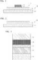
- FIG. 1 shows a power module 1 including the substrate 10 for a power module as the present embodiment.
- the power module 1 includes the substrate 10 for a power module provided with the circuit layer 12 and a semiconductor element 3 bonded to one surface (upper surface in FIG. 1 ) of the circuit layer 12 through a bonding layer 2.
- the substrate 10 for a power module includes the ceramic substrate 11 and the circuit layer 12 provided on one surface (upper surface in FIG. 2 ) of the ceramic substrate 11.
- the ceramic substrate 11 is constituted with ceramics such as aluminum nitride (AlN), silicon nitride (Si 3 N 4 ), and alumina (Al 2 O 3 ) having high insulating properties.
- the ceramic substrate 11 is constituted with aluminum nitride (AlN) having excellent heat radiation properties.
- the thickness of the ceramic substrate 11 is set within a range of 0.2 to 1.5 mm. In the present embodiment, the thickness of the ceramic substrate 11 is set to be 0.635 mm.
- the circuit layer 12 is formed by bonding a metal sheet formed of Cu or a Cu alloy having conductivity to one surface of the ceramic substrate 11.
- the circuit layer 12 is formed by laminating a Cu-P-Sn-based brazing material 24 and the Cu foil 22 formed of oxygen-free copper, to which a Ti material 25 is bonded, on one surface of the ceramic substrate 11 and performing a heat treatment such that the Cu foil 22 is bonded to the ceramic substrate 11 (see FIG. 5 ).
- a Cu-P-Sn-based brazing material 24 As the Cu-P-Sn-based brazing material 24, a Cu-P-Sn-Ni brazing material is used as the Cu-P-Sn-Ni brazing material is used as the Cu-P-Sn-Ni brazing material is used as the Cu-P-Sn-Ni brazing material is used as the Cu-P-Sn-Ni brazing material is used as the Cu-P-Sn-Ni brazing material is used as the Cu-P-Sn-Ni brazing material is used as the Cu-P-Sn-Ni brazing material is used as the Cu-P-Sn-Ni brazing material
- a structure in which Sn is diffused in Cu is established on the ceramic substrate 11 side on the circuit layer 12.
- the thickness of the circuit layer 12 is set within a range equal to or greater than 0.1 mm and equal to or smaller than 1.0 mm. In the present embodiment, the thickness of the circuit layer 12 is set to be 0.3 mm.
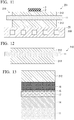
- FIG. 3 is a view schematically describing a bonded interface between the ceramic substrate 11 and the circuit layer 12.
- a Cu-Sn layer 14 which is positioned on the ceramic substrate 11 side
- a first intermetallic compound layer 16 which is positioned on the circuit layer 12 side and contains Cu and Ti
- a second intermetallic compound layer 17 which is positioned between the first intermetallic compound layer 16 and the Cu-Sn layer 14 and contains P and Ti are formed.
- the Cu-Sn layer 14 is a layer in which Sn forms a solid solution in Cu.
- P contained in the Cu-P-Sn-based brazing material 24 into the second intermetallic compound layer 17 the Cu-Sn layer 14 is formed.
- the first intermetallic compound layer 16 is a layer formed by the interdiffusion between Cu of the circuit layer 12 and Ti of the Ti material 25.
- the diffusion of Cu and Ti is diffusion in solids.
- the first intermetallic compound layer 16 has one or more phases among a Cu 4 Ti phase, a Cu 3 Ti 2 phase, a Cu 4 Ti 3 phase, a CuTi phase, and a CuTi 2 phase.
- the first intermetallic compound layer 16 has a Cu 4 Ti phase, a Cu 3 Ti 2 phase, a Cu 4 Ti 3 phase, a CuTi phase, and a CuTi 2 phase.
- the thickness of the first intermetallic compound layer 16 is set within a range equal to or greater than 0.2 ⁇ m and equal to or smaller than 6 ⁇ m.
- the second intermetallic compound layer 17 is formed by bonding of P contained in the Cu-P-Sn-based brazing material 24 to Ti contained in the Ti material 25.
- the Cu-P-Sn-based brazing material 24 contains Ni. Therefore, the second intermetallic compound layer 17 has one or more kinds of phases among a P-Ni-Ti phase, a P-Ti phase, and a Cu-Ni-Ti phase. Specifically, the second intermetallic compound layer 17 has a P-Ni-Ti phase.
- the thickness of the second intermetallic compound layer 17 is within a range equal to or greater than 0.5 ⁇ m and equal to or smaller than 4 ⁇ m.
- the semiconductor element 3 is constituted with a semiconductor material such as Si.
- the semiconductor element 3 and the circuit layer 12 are bonded to each other through a bonding layer 2.
- the bonding layer 2 is formed of a solder material based on Sn-Ag, Sn-In, or Sn-Ag-Cu, for example.
- the Cu foil 22 which will become the circuit layer 12 and the Ti material 25 are laminated, disposed in a vacuum heating furnace in a state where pressure (1 to 35 kgf/cm 2 ) is applied thereto in the lamination direction, and heated such that the Cu foil 22 and the Ti material 25 are bonded to each other by diffusion in solids, thereby obtaining a Cu-Ti bonded body 27 (CuTi diffusing step S01).
- the thickness of the Ti material 25 is within a range equal to or greater than 0.4 ⁇ m and equal to or smaller than 5 ⁇ m. In a case where the thickness of the Ti material 25 is equal to or greater than 0.4 ⁇ m and less than 1 ⁇ m, it is preferable that the Ti material 25 is deposited by vapor deposition or sputtering. In a case where the thickness of the Ti material 25 is equal to or greater than 1 ⁇ m and equal to or smaller than 5 ⁇ m, it is preferable to use a foil material.
- the lower limit of the thickness of the Ti material 25 is preferably equal to or greater than 0.4 ⁇ m, and more preferably equal to or greater than 0.5 ⁇ m.
- the upper limit of the thickness of the Ti material 25 is preferably equal to or smaller than 1.5 ⁇ m, and more preferably equal to or smaller than 0.7 ⁇ m.
- a Ti foil having a thickness of 1 ⁇ m and a purity of 99.8 mass% is used as the Ti material 25 as the Ti material 25, a Ti foil having a thickness of 1 ⁇ m and a purity of 99.8 mass% is used as the Ti material 25 as the Ti material 25, a Ti foil having a thickness of 1 ⁇ m and a purity of 99.8 mass% is used.
- the Ti material 25 and the Cu foil 22 are bonded to each other by diffusion in solids, and a laminated structure of the Cu foil 22 and an intermediate Ti layer 26 is established. Between the intermediate Ti layer 26 and the Cu foil 22, a first intermediate intermetallic compound layer containing Cu and Ti is formed. At this time, not all the Ti material 25 is consumed for forming the first intermediate intermetallic compound layer, and a portion of the Ti material 25 remains.
- the thickness of the intermediate Ti layer 26 is within a range equal to or greater than 0.1 ⁇ m and equal to or smaller than 3 ⁇ m.
- the lower limit of the thickness of the intermediate Ti layer 26 is preferably equal to or greater than 0.2 ⁇ m, and more preferably equal to or greater than 0.4 ⁇ m.
- the upper limit of the thickness of the intermediate Ti layer 26 is preferably equal to or smaller than 1.5 ⁇ m, and more preferably equal to or smaller than 1 ⁇ m.
- the thickness of the first intermediate intermetallic compound layer is preferably equal to or greater than 0.1 ⁇ m and equal to or smaller than 6 ⁇ m.
- the internal pressure of the vacuum heating furnace is set within a range equal to or higher than 10 -6 Pa and equal to or lower than 10 -3 Pa
- the heating temperature is set within a range equal to or higher than 600°C and equal to or lower than 670°C
- the heating time is set within a range equal to or longer than 30 minutes and equal to or shorter than 360 minutes.
- the heating temperature is set to be equal to or higher than 600°C and the heating time is set to be equal to or longer than 30 minutes
- the first intermediate intermetallic compound layer can be sufficiently formed.
- the heating temperature is set to be equal to or lower than 670°C, and the heating time is set to be equal to or shorter than 360 minutes, it is possible to inhibit the formed first intermediate intermetallic compound layer from becoming unnecessarily thick.
- the lower limit of the heating temperature is preferably equal to or higher than 610°C, and more preferably equal to or higher than 620°C.
- the upper limit of the heating temperature is preferably equal to or lower than 650°C, and more preferably equal to or lower than 640°C.
- the lower limit of the heating time is preferably equal to or longer than 15 minutes, and more preferably equal to or longer than 60 minutes.
- the upper limit of the heating time is preferably equal to or shorter than 120 minutes, and more preferably equal to or shorter than 90 minutes.
- the load applied in the lamination direction is preferably within a range equal to or higher than 0.294 MPa and equal to or lower than 1.96 MPa (equal to or higher than 3 kgf/cm 2 and equal to or lower than 20 kgf/cm 2 ).
- the load is more preferably within a range equal to or higher than 0.490 MPa and equal to or lower than 1.47 MPa, and even more preferably within a range equal to or higher than 1.18 MPa and equal to or lower than 1.47 MPa.
- the Cu-P-Sn-based brazing material 24 and the Cu-Ti bonded body 27 are laminated in this order on one surface (upper surface in FIG. 5 ) of the ceramic substrate 11 (laminating step S02). At this time, the Cu-Ti bonded body 27 is laminated such that the intermediate Ti layer 26 and the Cu-P-Sn-based brazing material 24 face each other.
- the composition of the Cu-P-Sn-based brazing material 24 is Cu-7 mass% P-15 mass% Sn-10 mass% Ni.
- the solidus temperature (melting start temperature) of the Cu-P-Sn-based brazing material 24 is 580°C.
- a foil material is used, and the thickness thereof is within a range equal to or greater than 5 ⁇ m and equal to or smaller than 150 ⁇ m.
- the ceramic substrate 11, the Cu-P-Sn-based brazing material 24, and the Cu-Ti bonded body 27 are put into a vacuum heating furnace in a state where pressure (1 to 35 kgf/cm 2 ) is applied thereto in the lamination direction, and heated (heat treatment step S03).
- the internal pressure of the vacuum heating furnace is set within a range equal to or higher than 10 -6 Pa and equal to or lower than 10 -3 Pa
- the heating temperature is set within a range equal to or higher than 600°C and equal to or lower than 700°C
- the heating time is set within a range equal to or longer than 15 minutes and equal to or shorter than 120 minutes.
- the Cu-P-Sn-based brazing material 24 is melted and forms a liquid phase.
- the intermediate Ti layer 26 is melted into the liquid phase, and the liquid phase is solidified.
- P and Ni contained in the Cu-P-Sn-based brazing material 24 are bonded to Ti of the intermediate Ti layer 26. Consequently, the second intermetallic compound layer 17 is formed, and the Cu-Sn layer 14 is formed on the ceramic substrate 11 side.
- the first intermetallic compound layer 16 is formed by the remaining first intermediate intermetallic compound layer.
- the thickness of the intermediate Ti layer 26 is within a range equal to or greater than 0.1 ⁇ m and equal to or smaller than 3 ⁇ m. Accordingly, the intermediate Ti layer 26 is totally melted into the liquid phase of the Cu-P-Sn-based brazing material 24, and no intermediate Ti layer 26 remains in the bonded interface between the ceramic substrate 11 and the circuit layer 12.
- the circuit layer 12 is formed on one surface of the ceramic substrate 11, and the substrate 10 for a power module as the present embodiment is manufactured.
- the semiconductor element 3 is bonded to the upper surface of the circuit layer 12 of the substrate 10 for a power module through a solder material (semiconductor element-bonding step S04).
- the power module 1 according to the present embodiment is manufactured.
- the substrate 10 for a power module of the present embodiment constituted as above, in the bonded interface between the ceramic substrate 11 and the circuit layer 12, the first intermetallic compound layer 16 which is positioned on the circuit layer 12 side and contains Cu and Ti is formed. Therefore, through the first intermetallic compound layer 16, the circuit layer 12 and the second intermetallic compound layer 17 can be reliably bonded to each other. As a result, even though the substrate 10 for a power module is used in a high-temperature environment, the brazing bonding strength between the circuit layer 12 and the ceramic substrate 11 can be secured.
- the Ti layer is not formed in the bonded interface between the ceramic substrate 11 and the circuit layer 12. Accordingly, the thermal resistance in the lamination direction of the circuit layer 12 and the ceramic substrate 11 can be kept low, and the heat generated from the semiconductor element 3 mounted on the circuit layer 12 can be efficiently radiated.
- the thickness of the first intermetallic compound layer 16 is equal to or greater than 0.2 ⁇ m. Therefore, the brazing bonding strength between the circuit layer 12 and the ceramic substrate 11 can be reliably improved. Meanwhile, because the thickness of the first intermetallic compound layer 16 is equal to or smaller than 6 ⁇ m, it is possible to inhibit the occurrence of breaking in the first intermetallic compound layer 16.
- the lower limit of the thickness of the first intermetallic compound layer 16 is preferably equal to or greater than 0.5 ⁇ m, and more preferably equal to or greater than 1 ⁇ m. Furthermore, in order to reliably inhibit the occurrence of breaking in the first intermetallic compound layer 16, the upper limit of the thickness of the first intermetallic compound layer 16 is preferably equal to or smaller than 5 ⁇ m, and more preferably equal to or smaller than 3 ⁇ m. Note that because sometimes the diffusion of Ti proceeds due to the heating in the heat treatment step S03, the thickness of the first intermetallic compound layer 16 becomes larger than the thickness of the first intermediate intermetallic compound layer.
- the thickness of the second intermetallic compound layer 17 is equal to or greater than 0.5 ⁇ m. Accordingly, the brazing bonding strength between the circuit layer 12 and the ceramic substrate 11 can be reliably improved. Meanwhile, because the thickness of the second intermetallic compound layer 17 is equal to or smaller than 4 ⁇ m, it is possible to inhibit the occurrence of breaking in the second intermetallic compound layer 17.
- the lower limit of the thickness of the second intermetallic compound layer 17 is preferably equal to or greater than 1 ⁇ m, and more preferably equal to or greater than 2 ⁇ m. Furthermore, in order to reliably inhibit the occurrence of breaking in the second intermetallic compound layer 17, the upper limit of the thickness of the second intermetallic compound layer 17 is preferably equal to or smaller than 3.5 ⁇ m, and more preferably equal to or smaller than 3 ⁇ m.
- the method for manufacturing the power module substrate of the present embodiment includes the CuTi diffusing step S01 in which the Cu foil 22 which will become the circuit layer 12 and the Ti material 25 are laminated, disposed in a vacuum heating furnace in a state where pressure (1 to 35 kgf/cm 2 ) is applied thereto in the lamination direction, and heated so as to bond the Cu foil 22 and the Ti material 25 to each other by diffusion in solids and to obtain the Cu-Ti bonded body 27. Accordingly, it is possible to reliably form the first intermediate intermetallic compound layer containing Cu and Ti between the Cu foil 22 and the intermediate Ti layer 26.
- the thickness of the intermediate Ti layer 26 is within a range equal to or greater than 0.1 ⁇ m and equal to or smaller than 3 ⁇ m. Accordingly, in the heat treatment step S03 as the next step, the intermediate Ti layer 26 and the Cu-P-Sn-based brazing material 24 can be reacted with each other.
- the Cu-P-Sn-based brazing material 24 is not laminated. Accordingly, the heating temperature and the heating time can be relatively freely set.
- the method for manufacturing the power module substrate of the present embodiment also includes the heat treatment step S03 of putting the ceramic substrate 11, the Cu-P-Sn-based brazing material 24, and the Cu-Ti bonded body 27 into a vacuum heating furnace in a state where pressure (1 to 35 kgf/cm 2 ) is applied thereto in the lamination direction, and performing heating. Accordingly, by reacting Ti of the intermediate Ti layer 26 with the Cu-P-Sn-based brazing material 24, it is possible to form the second intermetallic compound layer 17 and to reliably bond the circuit layer 12 and the ceramic substrate 11 to each other.
- the pressure applied in the heat treatment step S03 is equal to or higher than 1 kgf/cm 2 , it is possible to bring the ceramic substrate 11 into close contact with the liquid phase of the Cu-P-Sn-based brazing material 24 and to excellently bond the ceramic substrate 11 and the Cu-Sn layer 14 to each other.
- the applied pressure is set within a range equal to or higher than 1 kgf/cm 2 and equal to or lower than 35 kgf/cm 2 .
- FIG. 6 shows a power module 101 including a substrate 110 for a power module according to the second embodiment.
- the power module 101 includes the substrate 110 for a power module provided with a circuit layer 112 and a metal layer 113, the semiconductor element 3 bonded to one surface (upper surface in FIG. 6 ) of the circuit layer 112 through the bonding layer 2, and a heat sink 130 disposed on the other side (lower side in FIG. 6 ) of the metal layer 113.
- the substrate 110 for a power module includes the ceramic substrate 11, the circuit layer 112 provided on one surface (upper surface in FIG. 7 ) of the ceramic substrate 11, and the metal layer 113 provided on the other surface (lower surface in FIG. 7 ) of the ceramic substrate 11.
- the ceramic substrate 11 is constituted with aluminum nitride (A1N) having excellent heat radiation properties as in the first embodiment.
- the circuit layer 112 is formed by laminating a Cu-P-Sn-based brazing material 124, the Ti material 25, and a Cu foil 122 formed of oxygen-free copper in this order on one surface of the ceramic substrate 11, and performing a heat treatment so as to bond the Cu foil 122 to the ceramic substrate 11 (see FIG. 10 ).
- the thickness of the circuit layer 112 is set within a range equal to or greater than 0.1 mm and equal to or smaller than 1.0 mm. In the present embodiment, the thickness of the circuit layer 112 is set to be 0.3 mm.
- the metal layer 113 is formed.
- the metal layer 113 is formed (see FIG. 10 ).
- the thickness of the metal layer 113 is set within a range equal to or greater than 0.1 mm and equal to or smaller than 1.0 mm. In the present embodiment, the thickness of the metal layer 113 is set to be 0.3 mm.
- the Cu-P-Sn-based brazing material 124 specifically, a Cu-P-Sn-Ni brazing material is used.
- FIG. 8 is a view schematically describing the bonded interface between the ceramic substrate 11 and the circuit layer 112 (metal layer 113).
- the Cu-Sn layer 14 which is positioned on a ceramic substrate 111 side
- the first intermetallic compound layer 16 which is positioned on the circuit layer 112 (metal layer 113) side and contains Cu and Ti
- the second intermetallic compound layer 17 which is positioned between the first intermetallic compound layer 16 and the Cu-Sn layer 14 and contains P and Ti are formed.
- a Ti layer 15 is formed between the first intermetallic compound layer 16 and the second intermetallic compound layer 17.
- the thickness of the Ti layer 15 is equal to or smaller than 0.5 ⁇ m.
- the thickness of the first intermetallic compound layer 16 is within a range equal to or greater than 0.2 ⁇ m and equal to or smaller than 6 ⁇ m.
- the thickness of the second intermetallic compound layer 17 is within a range equal to or greater than 0.5 ⁇ m and equal to or smaller than 4 ⁇ m.
- the heat sink 130 dissipates the heat from the aforementioned substrate 110 for a power module.
- the heat sink 130 is constituted with Cu or a Cu alloy.
- the heat sink 130 is constituted with phosphorus deoxidized copper.
- the heat sink 130 is provided with passages 131 for a cooling fluid to flow through the passages.
- the heat sink 130 and the metal layer 113 are bonded to each other by a solder layer 132 formed of a solder material.
- the Cu-P-Sn-based brazing material 124, the Ti material 25, and the Cu foil 122 which will become the circuit layer 112 are laminated in this order on one surface (upper surface in FIG. 10 ) of the ceramic substrate 11, and the Cu-P-Sn-based brazing material 124, the Ti material 25, and the Cu foil 123 which will become the metal layer 113 are laminated in this order on the other surface (lower surface in FIG. 10 ) of the ceramic substrate 11 (laminating step S101).
- the Cu-P-Sn-based brazing material 124 is disposed on the ceramic substrate 11 side, and the Ti material 25 is disposed on the Cu foil 122 side and the Cu foil 123 side.
- the composition of the Cu-P-Sn-based brazing material 124 is Cu-6.3 mass% P-9.3 mass% Sn-7 mass% Ni.
- the solidus temperature (melting start temperature) of the Cu-P-Sn-based brazing material 124 is 600°C.
- a foil material is used, and the thickness thereof is within a range equal to or greater than 5 ⁇ m and equal to or smaller than 150 ⁇ m.
- the thickness of the Ti material 25 is within a range equal to or greater than 0.4 ⁇ m and equal to or smaller than 5 ⁇ m. In a case where the thickness of the Ti material 25 is equal to or greater than 0.4 ⁇ m and less than 1 ⁇ m, it is preferable to deposit the Ti material 25 by vapor deposition or sputtering. In a case where the thickness of the Ti material 25 is equal to or greater than 1 ⁇ m and equal to or smaller than 5 ⁇ m, it is preferable to use a foil material.
- the lower limit of the thickness of the Ti material 25 is preferably equal to or greater than 0.4 ⁇ m, and more preferably equal to or greater than 0.5 ⁇ m.
- the upper limit of the thickness of the Ti material 25 is preferably equal to or smaller than 1.5 ⁇ m, and more preferably equal to or smaller than 0.7 ⁇ m.
- a Ti foil having a thickness of 1 ⁇ m and a purity of 99.8 mass% is used as the Ti material 25 as the Ti material 25, a Ti foil having a thickness of 1 ⁇ m and a purity of 99.8 mass% is used as the Ti material 25 as the Ti material 25, a Ti foil having a thickness of 1 ⁇ m and a purity of 99.8 mass% is used.
- the Cu foil 122, the Ti material 25, the Cu-P-Sn-based brazing material 124, the ceramic substrate 11, the Cu-P-Sn-based brazing material 124, the Ti material 25, and the Cu foil 123 are put into a vacuum heating furnace in a state where pressure (equal to or higher than 1 kgf/cm 2 and equal to or lower than 35 kgf/cm 2 ) is applied thereto in the lamination direction, and heated at a temperature lower than the melting start temperature of the Cu-P-Sn-based brazing material 124 (first heat treatment step S102).
- the bonding of the Ti material 25 to the Cu foil 122 and the bonding of the Ti material 25 to the Cu foil 123 are performed by diffusion in solids, and the first intermetallic compound layer 16 containing Cu and Ti is formed between the Ti material 25 and the Cu foil 122 and between the Ti material 25 and the Cu foil 123.
- the internal pressure of the vacuum heating furnace is set within a range equal to or higher than 10 -6 Pa and equal to or lower than 10 -3 Pa
- the heating temperature is set within a range equal to or higher than 580°C and equal to or lower than 670°C
- the heating time is set within a range equal to or longer than 30 minutes and equal to or shorter than 240 minutes.
- the heating temperature in the first heat treatment step S102 is 10°C lower than the melting start temperature (solidus temperature) of the Cu-P-Sn-based brazing material 124.
- the first intermetallic compound layer 16 can be sufficiently formed. Furthermore, in a case where the heating temperature is equal to or lower than 670°C, and the heating time is equal to or shorter than 240 minutes, it is possible to inhibit the formed first intermetallic compound layer 16 from becoming unnecessarily thick.
- the lower limit of the heating temperature is preferably equal to or higher than 610°C, and more preferably equal to or higher than 620°C.
- the upper limit of the heating temperature is preferably equal to or lower than 650°C, and more preferably equal to or lower than 640°C.
- the lower limit of the heating time is preferably equal to or longer than 15 minutes, and more preferably equal to or longer than 60 minutes.
- the upper limit of the heating time is preferably equal to or shorter than 120 minutes, and more preferably equal to or shorter than 90 minutes.
- the Cu foil 122, the Ti material 25, the Cu-P-Sn-based brazing material 124, the ceramic substrate 11, the Cu-P-Sn-based brazing material 124, the Ti material 25, and the Cu foil 123 are heated at a temperature equal to or higher than the melting start temperature of the Cu-P-Sn-based brazing material 124 in a state where pressure (equal to or higher than 1 kgf/cm 2 and equal to or lower than 35 kgf/cm 2 ) is applied thereto in the lamination direction (second heat treatment step S103).
- the internal pressure of the vacuum heating furnace is set within a range equal to or higher than 10 -6 Pa and equal to or lower than 10 -3 Pa
- the heating temperature is set within a range equal to or higher than 600°C and equal to or lower than 700°C
- the heating time is set within a range equal to or longer than 15 minutes and equal to or shorter than 120 minutes.
- the second heat treatment step S103 in order to reliably melt the Cu-P-Sn-based brazing material 124, it is preferable that heating is performed at a temperature equal to or higher than the solidus temperature of the Cu-P-Sn-based brazing material 124 + 10°C.
- the Cu-P-Sn-based brazing material 124 is melted and forms a liquid phase.
- the Ti material 25 is melted into the liquid phase, and the liquid phase is solidified.
- the ceramic substrate 11 is bonded to the Cu foil 122 and the Cu foil 123.
- P and Ni contained in the Cu-P-Sn-based brazing material 124 are bonded to Ti of the Ti material 25.
- the second intermetallic compound layer 17 is formed, and the Cu-Sn layer 14 is formed on the ceramic substrate 11 side.
- the Ti material 25 remains without being melted into the liquid phase of the Cu-P-Sn-based brazing material 124.
- the Ti layer 15 is formed between the first intermetallic compound layer 16 and the second intermetallic compound layer 17.
- the circuit layer 112 is formed on one surface of the ceramic substrate 11, and the metal layer 113 is formed on the other surface of the ceramic substrate 11. In this way, the substrate 110 for a power module as the present embodiment is manufactured.
- heat sink bonding step S104 the heat sink 130 is bonded to the lower surface of the metal layer 113 of the substrate 110 for a power module through a solder material (heat sink bonding step S104).
- the semiconductor element 3 is bonded to the upper surface of the circuit layer 112 of the substrate 110 for a power module through a solder material (semiconductor element-bonding step S105).
- the power module 101 according to the present embodiment is manufactured.
- the first intermetallic compound layer 16 which is positioned on the circuit layer 112 side and the metal layer 113 side and contains Cu and Ti is formed. Accordingly, through the first intermetallic compound layer 16, the second intermetallic compound layers 17 can be reliably bonded to the circuit layer 112 and the metal layer 113. Therefore, even though the substrate 110 for a power module is used in a high-temperature environment, the brazing bonding strength between the circuit layer 112 and the ceramic substrate 11 and between the metal layer 113 and the ceramic substrate 11 can be secured.
- the Ti layer 15 is formed, but the thickness of the Ti layer 15 is equal to or smaller than 0.5 ⁇ m. Accordingly, the thermal resistance in the lamination direction of the circuit layer 112, the ceramic substrate 11, and the metal layer 113 can be kept low, and the heat generated from the semiconductor element 3 mounted on the circuit layer 112 can be efficiently radiated.
- the thickness of the first intermetallic compound layer 16 is equal to or greater than 0.2 ⁇ m. Accordingly, the brazing bonding strength between the circuit layer 112 and the ceramic substrate 11 and between the metal layer 113 and the ceramic substrate 11 can be reliably improved. Meanwhile, because the thickness of the first intermetallic compound layer 16 is equal to or smaller than 6 ⁇ m, it is possible to inhibit the occurrence of breaking in the first intermetallic compound layer 16.
- the thickness of the second intermetallic compound layer 17 is equal to or greater than 0.5 ⁇ m. Accordingly, the brazing bonding strength between the circuit layer 112 and the ceramic substrate 11 and between the metal layer 113 and the ceramic substrate 11 can be reliably improved. Meanwhile, because the thickness of the second intermetallic compound layer 17 is equal to or smaller than 4 ⁇ m, it is possible to inhibit the occurrence of breaking in the second intermetallic compound layer 17.
- the method for manufacturing the power module substrate of the present embodiment includes a first heat treatment step S102 of putting the Cu foil 122, the Ti material 25, the Cu-P-Sn-based brazing material 124, the ceramic substrate 11, the Cu-P-Sn-based brazing material 124, the Ti material 25, and the Cu foil 123 into a vacuum heating furnace in a state where pressure (equal to or higher than 1 kgf/cm 2 and equal to or lower than 35 kgf/cm 2 ) is applied thereto in the lamination direction and performing heating at a temperature lower than the melting start temperature of the Cu-P-Sn-based brazing material 124. Accordingly, the first intermetallic compound layer 16 containing Cu and Ti can be reliably formed between the Cu foil 122 which will become the circuit layer 112 and the Ti material 25 and between the Cu foil 123 which will become the metal layer 113 and the Ti material 25.
- the method for manufacturing the power module substrate of the present embodiment includes the second heat treatment step S103 of performing heating after the first heat treatment step S102 at a temperature equal to or higher than the melting start temperature of the Cu-P-Sn-based brazing material 124 so as to form the Cu-Sn layer 14 in which Sn forms a solid solution in Cu and the second intermetallic compound layer 17 which is positioned between the first intermetallic compound layer 16 and the Cu-Sn layer 14 and contains P and Ti. Accordingly, by causing Ti of the Ti material 25 to react with the Cu-P-Sn-based brazing material 124, the second intermetallic compound layer 17 can be formed, and the ceramic substrate 11 can be reliably bonded to the circuit layer 112 and the metal layer 113.
- the pressure applied in the second heat treatment step S103 is equal to or higher than 1 kgf/cm 2 , it is possible to bring the ceramic substrate 11 into close contact with the liquid phase of the Cu-P-Sn-based brazing material 124 and to excellently bond the ceramic substrate 11 and the Cu-Sn layer 14 to each other. Furthermore, in a case where the applied pressure is equal to or lower than 35 kgf/cm 2 , the occurrence of breaking in the ceramic substrate 11 can be inhibited. For these reasons, in the present embodiment, the applied pressure is set within a range equal to or higher than 1 kgf/cm 2 and equal to or lower than 35 kgf/cm 2 .
- the method for manufacturing the substrate 110 for a power module according to the present embodiment adopts a constitution in which the bonding of the circuit layer 112 to one surface of the ceramic substrate 11 and the bonding of the metal layer 113 to the other surface of the ceramic substrate 11 are simultaneously performed. Therefore, it is possible to simplify the manufacturing process and to reduce the manufacturing cost.
- FIG. 11 shows a power module 201 including a substrate 210 for a power module according to the third embodiment.
- the power module 201 includes the substrate 210 for a power module provided with a circuit layer 212 and a metal layer 213, the semiconductor element 3 bonded to one surface (upper surface in FIG. 11 ) of the circuit layer 212 through the bonding layer 2, and a heat sink 230 bonded to the other side (lower side in FIG. 11 ) of the substrate 210 for a power module.
- the substrate 210 for a power module includes the ceramic substrate 11, the circuit layer 212 provided on one surface (upper surface in FIG. 12 ) of the ceramic substrate 11, and the metal layer 213 provided on the other surface (lower surface in FIG. 12 ) of the ceramic substrate 11.
- the ceramic substrate 11 is constituted with aluminum nitride (A1N) having excellent heat radiation properties as in the first embodiment.
- the circuit layer 212 is formed by laminating a Cu-P-Sn-based brazing material 224, the Ti material 25, and a Cu foil 222 formed of oxygen-free copper on one surface of the ceramic substrate 11 and performing a heat treatment such that the Cu foil 222 is bonded to the ceramic substrate 11 (see FIG. 15 ).
- the thickness of the circuit layer 212 is set within a range equal to or greater than 0.1 mm and equal to or smaller than 1.0 mm. In the present embodiment, the thickness of the circuit layer 212 is set to be 0.3 mm.
- the Cu-P-Sn-based brazing material 224 specifically, a Cu-P-Sn-Ni brazing material is used.
- the Cu-Sn layer 14 which is positioned on the ceramic substrate 11 side
- the first intermetallic compound layer 16 which is positioned on the circuit layer 212 side and contains Cu and Ti
- the second intermetallic compound layer 17 which is positioned between the first intermetallic compound layer 16 and the Cu-Sn layer 14 and contains P and Ti are formed.
- the Ti layer 15 is formed between the first intermetallic compound layer 16 and the second intermetallic compound layer 17. Furthermore, between the first intermetallic compound layer 16 and the second intermetallic compound layer 17, the Ti layer 15 is formed.
- the thickness of the Ti layer 15 is equal to or smaller than 0.5 ⁇ m.
- the metal layer 213 is formed by bonding an Al sheet formed of Al or an Al alloy to the other surface of the ceramic substrate 11.
- the metal layer 213 is formed by bonding an Al sheet 223 having a purity equal to or higher than 99.99 mass% to the other surface of the ceramic substrate 11 (see FIG. 15 ).
- the thickness of the metal layer 213 is set within a range equal to or greater than 0.1 mm and equal to or smaller than 3.0 mm. In the present embodiment, the thickness of the metal layer 213 is set to be 1.6 mm.
- the heat sink 230 is constituted with Al or an Al alloy.
- the heat sink 230 is constituted with A6063 (Al alloy).
- the heat sink 230 is provided with passages 231 for a cooling fluid to flow through the passages.
- the heat sink 230 and the metal layer 213 are bonded to each other by an Al-Si-based brazing material.
- the Cu foil 222 which will become the circuit layer 212 and the Ti material 25 are laminated, disposed in a vacuum heating furnace in a state where pressure (1 to 35 kgf/cm 2 ) is applied thereto in the lamination direction, and heated such that the Cu foil 222 and the Ti material 25 are bonded to each other by diffusion in solids, thereby obtaining a Cu-Ti bonded body 227 (CuTi diffusing step S201).
- the thickness of the Ti material 25 is within a range equal to or greater than 0.4 ⁇ m and equal to or smaller than 5 ⁇ m. In a case where the thickness of the Ti material 25 is equal to or greater than 0.4 ⁇ m and less than 1 ⁇ m, it is preferable to deposit the Ti material 25 by vapor deposition or sputtering. In a case where the thickness of the Ti material 25 is equal to or greater than 1 ⁇ m and equal to or smaller than 5 ⁇ m, it is preferable to use a foil material.
- the lower limit of the thickness of the Ti material 25 is preferably equal to or greater than 0.4 ⁇ m, and more preferably equal to or greater than 0.5 ⁇ m.
- the upper limit of the thickness of the Ti material 25 is preferably equal to or smaller than 1.5 ⁇ m, and more preferably equal to or smaller than 0.7 ⁇ m.
- the Ti material 25 a Ti foil having a thickness of 1.4 ⁇ m and a purity of 99.8 mass% is used.
- the internal pressure of the vacuum heating furnace is set within a range equal to or higher than 10 -6 Pa and equal to or lower than 10 -3 Pa
- the heating temperature is set within a range equal to or higher than 600°C and equal to or lower than 670°C
- the heating time is set within a range equal to or longer than 30 minutes and equal to or shorter than 360 minutes.
- the heating temperature and the heating time in the CuTi diffusing step S201 are equal to or higher than 600°C and equal to or longer than 30 minutes respectively
- the first intermediate intermetallic compound layer can be sufficiently formed.
- the heating temperature is equal to or lower than 655°C and the heating time is equal to or shorter than 360 minutes, it is possible to inhibit the formed first intermediate intermetallic compound layer from becoming unnecessarily thick.
- the lower limit of the heating temperature is preferably equal to or higher than 610°C, and more preferably equal to or higher than 620°C.
- the upper limit of the heating temperature is preferably equal to or lower than 650°C, and more preferably equal to or lower than 640°C.
- the lower limit of the heating time is preferably equal to or longer than 15 minutes, and more preferably equal to or longer than 60 minutes.
- the upper limit of the heating time is preferably equal to or shorter than 120 minutes, and more preferably equal to or shorter than 90 minutes.
- the load applied in the lamination direction in the CuTi diffusing step S201 is within a range equal to or higher than 0.294 MPa and equal to or lower than 1.96 MPa (equal to or higher than 3 kgf/cm 2 and equal to or lower than 20 kgf/cm 2 ).
- the applied load is more preferably within a range equal to or higher than 0.490 MPa and equal to or lower than 1.47 MPa, and even more preferably within a range equal to or higher than 1.18 MPa and equal to or lower than 1.47 MPa.
- the Ti material 25 and the Cu foil 222 are bonded to each other by diffusion in solids, and a laminated structure of the Cu foil 222 and the intermediate Ti layer 26 is established. Between the intermediate Ti layer 26 and the Cu foil 222, the first intermediate intermetallic compound layer containing Cu and Ti is formed. At this time, not all the Ti material 25 is consumed for forming the first intermediate intermetallic compound layer, and a portion of the Ti material 25 remains.
- the thickness of the intermediate Ti layer 26 is within a range equal to or greater than 0.1 ⁇ m and equal to or smaller than 3 ⁇ m.
- the lower limit of the thickness of the intermediate Ti layer 26 is preferably equal to or greater than 0.2 ⁇ m, and more preferably equal to or greater than 0.4 ⁇ m.
- the upper limit of the thickness of the intermediate Ti layer 26 is preferably equal to or smaller than 1.5 ⁇ m, and more preferably equal to or smaller than 0.7 ⁇ m.
- the thickness of the first intermediate intermetallic compound layer is preferably equal to or greater than 0.1 ⁇ m and equal to or smaller than 6 ⁇ m.
- the Cu-P-Sn-based brazing material 224, the Ti material 25, and the Cu foil 222 are laminated in this order on one surface (upper surface in FIG. 15 ) of the ceramic substrate 11, and the metal layer 213 and an Al sheet 223 are laminated in this order on the other surface (lower surface in FIG. 14 ) of the ceramic substrate 11 through a bonding material 241.
- the heat sink 230 is laminated on the lower side of the Al sheet 223 through a bonding material 242 (laminating step S202).
- the Cu-Ti bonded body 227 is laminated such that the intermediate Ti layer 26 and the Cu-P-Sn-based brazing material 224 face each other.
- the composition of Cu-P-Sn-based brazing material 224 is Cu-7 mass% P-15 mass% Sn-10 mass% Ni.
- the melting start temperature (solidus temperature) of the Cu-P-Sn-based brazing material 224 is 580°C.
- a foil material is used, and the thickness thereof is within a range equal to or greater than 5 ⁇ m and equal to or smaller than 150 ⁇ m.
- an Al-Si-based brazing material containing Si which is a melting point-lowering element is used as the bonding materials 241 and 242.
- Al-7.5 mass% Si brazing material is used.
- the ceramic substrate 11, the Cu-P-Sn-based brazing material 224, the Cu-Ti bonded body 227, the bonding material 241, the Al sheet 223, the bonding material 242, and the heat sink 230 are put into a vacuum heating furnace in a state where pressure (1 to 35 kgf/cm 2 ) is applied thereto in the lamination direction, and heated (heat treatment step S203).
- the internal pressure of the vacuum heating furnace is set within a range equal to or higher than 10 -6 Pa and equal to or lower than 10 -3 Pa
- the heating temperature is set within a range equal to or higher than 600°C and equal to or lower than 650°C
- the heating time is set within a range equal to or longer than 30 minutes and equal to or shorter than 240 minutes.
- the Cu-P-Sn-based brazing material 224 is melted and forms a liquid phase.
- the intermediate Ti layer 26 is melted into the liquid phase, and the liquid phase is solidified.
- the ceramic substrate 11 and the Cu foil 222 are bonded to each other.
- P and Ni contained in the Cu-P-Sn-based brazing material 224 are bonded to Ti of the intermediate Ti layer 26.
- the second intermetallic compound layer 17 is formed, and the Cu-Sn layer 14 is formed on the ceramic substrate 11 side.
- the first intermetallic compound layer 16 is formed by the remaining first intermediate intermetallic compound layer.
- the thickness of the intermediate Ti layer 26 is within a range equal to or greater than 0.1 ⁇ m and equal to or smaller than 3 ⁇ m. Accordingly, not all the intermediate Ti layer 26 is melted into the liquid phase of the Cu-P-Sn-based brazing material 224, and a portion of the intermediate Ti layer 26 remains and forms the Ti layer 15. However, because the formed Ti layer 15 is a thin layer having a thickness equal to or smaller than 0.5 ⁇ m, the thermal resistance in the lamination direction of the circuit layer 212, the ceramic substrate 11, and the metal layer 213 can be kept low, and the heat generated from the semiconductor element 3 mounted on the circuit layer 212 can be efficiently radiated.
- the thickness of the first intermetallic compound layer 16 becomes larger than the thickness of the first intermediate intermetallic compound layer.
- the thickness of the Ti layer 15 becomes smaller than the thickness of the intermediate Ti layer 26.
- the bonding material 241 is melted and forms a liquid phase, and the liquid phase is solidified.
- the ceramic substrate 11 and the Al sheet 223 are bonded to each other through the bonding material 241.
- the bonding material 242 is melted and forms a liquid phase, and the liquid phase is solidified.
- the Al sheet 223 and the heat sink 230 are bonded to each other through the bonding material 242.
- the substrate 210 for a power module as the present embodiment is manufactured.
- the semiconductor element 3 is bonded to the upper surface of the circuit layer 212 of the substrate 210 for a power module through a solder material (semiconductor element-bonding step S204).
- the power module 201 as the present embodiment is manufactured.
- the substrate 210 for a power module according to the present embodiment constituted as above exerts the same effects as those exerted by the substrates 10 and 110 for a power module described in the first present embodiment and the second present embodiment.
- the metal layer 213 is formed. Accordingly, the heat from the semiconductor element 3 can be efficiently dissipated through the metal layer 213.
- Al has a relatively low deformation resistance, in a case where a thermal cycle is loaded, the metal layer 213 can absorb a thermal stress caused between the substrate 210 for a power module and the heat sink 230, and the occurrence of breaking in the ceramic substrate 11 can be inhibited.
- the method for manufacturing the substrate 210 for a power module according to the present embodiment adopts a constitution in which the bonding of the circuit layer 212 to one surface of the ceramic substrate 11 and the bonding of the metal layer 213 to the other surface of the ceramic substrate 11 are simultaneously performed. Therefore, it is possible to simplify the manufacturing process and to reduce the manufacturing cost.
- thermoelectric element may be mounted on the circuit layer of the insulated circuit board so as to constitute a thermoelectric module.
- the bonding of the circuit layer to one surface of the ceramic substrate and the bonding of the metal layer to the other surface of the ceramic substrate are simultaneously performed.
- the circuit layer and the metal layer may be separately bonded.
- the circuit layer, the metal layer, and the heat sink are simultaneously bonded.
- a constitution may be adopted in which the circuit layer and the metal layer are bonded to the ceramic substrate, and then the metal layer and the heat sink are bonded to each other.
- the metal layer is bonded to the other surface of the ceramic substrate through the Al-Si-based brazing material.
- the metal layer may be bonded using a transient liquid phase (TLP) bonding method, Ag paste, or the like.
- TLP transient liquid phase
- a heat sink may not be bonded to the other surface side of the power module substrate.
- the first embodiment, the second embodiment, and the third embodiment a case where a Ti foil is used as a Ti material or a case where a Ti material is formed by vapor deposition or sputtering was described.
- a Cu member/Ti clad material in which Ti is provided on one surface of a Cu member can also be used.
- the Cu member/Ti clad material may be preheated such that a first intermetallic compound layer containing Cu and Ti is formed, or the first intermetallic compound layer may be formed in the interior of the Cu member/Ti clad material in the first heat treatment step.
- a Ti material/brazing material clad material in which a Cu-P-Sn-based brazing material is provided on one surface of a Ti material or a Cu member/Ti material/brazing material clad in which a Cu member, a Ti material, and a Cu-P-Sn-based brazing material are laminated in this order.
- Cu-P-Sn-Ni brazing material or a Cu-P-Sn brazing material is used as the Cu-P-Sn-based brazing material.
- other Cu-P-Sn-based brazing materials may also be used.
- the Cu-P-Sn-based brazing material used in the method for manufacturing the bonded body of the present invention will be specifically described.
- the content of P in the Cu-P-Sn-based brazing material is preferably equal to or greater than 3 mass% and equal to or smaller than 10 mass%.
- P is an element having an operation and effect of reducing the melting start temperature of the brazing material. In a case where P is oxidized, P oxide occurs. P is an element having an operation and effect of coating the surface of the brazing material with the P oxide so as to prevent the oxidation of the brazing material, and coating the surface of the molten brazing material with the P oxide having excellent fluidity so as to improve the wettability of the brazing material.
- the effect of reducing the melting start temperature of the brazing material may not be sufficiently obtained. Accordingly, the melting start temperature of the brazing material may be increased or the fluidity of the brazing material may become insufficient. As a result, the bonding properties between the ceramic substrate and the circuit layer may be reduced. Furthermore, in a case where the content of P is greater than 10 mass%, a large amount of brittle intermetallic compound may be formed. As a result, the bonding properties and the bonding reliability between the ceramic substrate and the circuit layer may be reduced.
- the content of P in the Cu-P-Sn-based brazing material is preferably within a range equal to or greater than 3 mass% and equal to or smaller than 10 mass%.
- the content of Sn in the Cu-P-Sn-based brazing material is preferably equal to or greater than 0.5 mass% and equal to or smaller than 25 mass%.
- Sn is an element having an operation and effect of reducing the melting start temperature of the brazing material.
- the melting start temperature of the brazing material can be reliably reduced.
- the content of Sn is equal to or smaller than 25 mass%, it is possible to inhibit the brazing material from becoming brittle at a low temperature and to improve the bonding reliability between the ceramic substrate and the circuit layer.
- the content of Sn in the Cu-P-Sn-based brazing material is preferably within a range equal to or greater than 0.5 mass% and equal to or smaller than 25 mass%.
- the Cu-P-Sn-based brazing material may contain one kind of element or two or more kinds of elements among Ni, Cr, Fe, and Mn in an amount equal to or greater than 2 mass% and equal to or smaller than 20 mass%.
- Ni, Cr, Fe, and Mn are elements having an operation and effect of inhibiting the formation of an intermetallic compound containing P in the interface between the ceramic substrate and the brazing material.
- the content of one kind of element or two or more kinds of elements among Ni, Cr, Fe, and Mn is equal to or greater than 2 mass%, the formation of an intermetallic compound containing P in the bonded interface between the ceramic substrate and the brazing material can be inhibited, and the bonding reliability between the ceramic substrate and the circuit layer can be improved. Furthermore, in a case where the content of one kind of element or two or more kinds of elements among Ni, Cr, Fe, and Mn is equal to or smaller than 20 mass%, it is possible to inhibit the increase of the melting start temperature of the brazing material, to inhibit the decrease of the fluidity of the brazing material, and to improve the bonding properties between the ceramic substrate and the circuit layer.
- the content of the element is preferably within a range equal to or greater than 2 mass% and equal to or smaller than 20 mass%.
- a Cu-P-Sn-based brazing material foil and a Ti material shown in Table 1 and a Cu foil formed of oxygen-free copper (thickness: 0.3 mm) were laminated in this order on one surface and the other surface of a ceramic substrate (40 mm ⁇ 40 mm, thickness of 0.635 mm for AlN and Al 2 O 3 substrates, thickness of 0.32 mm for Si 3 N 4 substrate) described in Table 1. Then, a load of 15 kgf/cm 2 was applied thereto in the lamination direction.
- the aforementioned laminate was put into a vacuum heating furnace (pressure: 10 -4 Pa), and as a first heat treatment step, the laminate was heated at a temperature for a time described in Table 1 (column of Heat treatment 1). Then, as the second heat treatment step, the laminate was heated at a temperature for a time described in Table 2 (column of Heat treatment 2) so as to bond the Cu foil to one surface and the other surface of the ceramic substrate and to form a circuit layer and a metal layer, thereby obtaining a power module substrate.
- the Cu foil for the circuit layer that was prepared for a 90° peel strength test which will be described later, had a size of 44 mm ⁇ 25 mm (here, the Cu foil protruded 5 mm from the end of the ceramic substrate), and the Cu foil for the circuit layer that was prepared for a thermal resistance test had a size of 37 mm ⁇ 37 mm.
- the Cu foil for the metal layer had a size of 37 mm ⁇ 37 mm.
- a Cu foil (thickness: 0.3 mm) formed of oxygen-free copper and a Ti material described in Table 1 were laminated.
- the laminate was put into a vacuum heating furnace (pressure: 10 -4 Pa) in a state where a pressure of 15 kgf/cm 2 was applied thereto in the lamination direction, and heated at a temperature for a time described in Table 1 (column of Heat treatment 1), thereby obtaining a Cu-Ti bonded body.
- the Cu-Ti bonded body was prepared for a circuit layer and a metal layer respectively.
- a Cu-P-Sn-based brazing material foil shown in Table 1 and the Cu-Ti bonded body were laminated in this order on one surface and the other surface of a ceramic substrate (40 mm ⁇ 40 mm, thickness of 0.635 mm for AlN and Al 2 O 3 substrates, thickness of 0.32 mm for Si 3 N 4 substrate) described in Table 1.
- the laminate was heated at a temperature for a time described in Table 2 (column of Heat treatment 2) so as to bond the Cu foil to one surface and the other surface of the ceramic substrate and to form a circuit layer and a metal layer, thereby preparing a power module substrate.
- Table 2 column of Heat treatment 2
- the size of each of the Cu foils for a circuit layer and a metal layer was the same as that described above.
- a Cu-P-Sn-based brazing material foil and a Ti material shown in Table 1 and a Cu foil (thickness: 0.3 mm) formed of oxygen-free copper were laminated in this order on one surface and the other surface of a ceramic substrate (40 mm ⁇ 40 mm ⁇ 0.635 mmt) described in Table 1, and a load of 15 kgf/cm 2 was applied thereto in the lamination direction.
- the aforementioned laminate was put into a vacuum heating furnace (pressure: 10 -4 Pa), and as the second heat treatment step, the laminate was heated at a temperature for a time described in Table 2 (column of Heat treatment 2) so as to bond the Cu foil to one surface and the other surface of the ceramic substrate and to form a circuit layer and a metal layer, thereby obtaining a power module substrate.
- Table 2 column of Heat treatment 2
- the size of each of the Cu foils for a circuit layer and a metal layer was the same as that in the examples of the present invention.
- the power module substrate obtained as above was evaluated in terms of 90° peel strength between the circuit layer and the ceramic substrate and thermal resistance in the lamination direction.
- the obtained power module substrate was evaluated in terms of the thickness of each of the first intermetallic compound layer, the Ti layer, and the second intermetallic compound layer in the bonded interface between the ceramic substrate and the circuit layer.
- the thickness of each of the first intermediate intermetallic compound layer and the intermediate Ti layer obtained after the heat treatment 1 was evaluated.
- Each of the power module substrates was left to stand for 500 hours at 150°C. Then, a portion of the circuit layer protruding from the ceramic substrate was folded at 90°, the circuit layer was pulled in a direction perpendicular to the ceramic substrate, and a maximum tensile load at which the circuit layer was peeled from the ceramic substrate was measured. A value obtained by dividing the load by a bonding length was adopted as 90° peel strength and described in Table 2. In the present example, the length (39 mm) of a side of the circuit layer in a portion where the circuit layer and the ceramic substrate were bonded to each other was adopted as the bonding length.
- the total area of the first intermetallic compound layer formed in the bonded interface, the area of the Ti layer, and the total area of the second intermetallic compound layer were measured in a visual field (length: 30 ⁇ m, width: 40 ⁇ m) of a 10,000X magnification, and each of the measured values was divided by the dimension of width of the visual field for measurement. The average of the values obtained as above from 5 visual fields was adopted as the thickness of each of the first intermetallic compound layer, the Ti layer, and the second intermetallic compound layer.
- the total area of the first intermediate intermetallic compound layer formed in the bonded interface and the total area of the intermediate Ti layer were measured in a visual field (length: 30 ⁇ m, width: 40 ⁇ m) of 10,000X magnification, and each of the measured values was divided by the dimension of width of the visual field for measurement. The average of the values obtained as above from 5 visual fields was adopted as the thickness of each of the first intermediate intermetallic compound layer and the intermediate Ti layer.
- a region in which the Ti concentration is within a range of 15 at% to 70 at% is regarded as the first intermetallic compound layer and the first intermediate intermetallic compound layer and regarded as not containing a solid solution.
- a region which contains at least P and Ti and in which the P concentration is within a range of 28 at% to 52 at% is regarded as the second intermetallic compound layer.
- Example 1 of the present invention AlN 6.3 9.3 Ni 7.0 Balance 600 2 A 590 30 - - Example 2 of the present invention AlN 6.3 9.3 Ni 7.0 Balance 600 5 A 590 240 - - Example 3 of the present in vention AlN 6.3 9.3 Ni 7.0 Balance 600 1.5 A 600 45 - - Example 4 of the present invention AlN 7.0 15.0 Ni 10.0 Balance 580 1 B 600 90 0.9 0.4 Example 5 of the present invention AlN 7.0 15.0 Ni 10.0 Balance 580 3 B 670 30 0.8 2.7
- Example 6 of the present invention AlN 6.3 9.3 Ni 7.0 Balance 600 0.7 B 630 60 0.6 0.5
- Example 7 Example 7
- Example 1 of the related art in which a thick Ti layer was formed it was confirmed that the 90° peel strength is high, but the thermal resistance in the lamination direction is high. Furthermore, in Example 2 of the related art in which no Ti layer was checked, it was confirmed that the first intermetallic compound layer is not formed, and the 90° peel strength is low.
- a Cu foil (thickness: 0.3 mm) formed of oxygen-free copper and a Ti material having a thickness of 3 mm were laminated, and the laminate was put into a vacuum heating furnace (pressure: 10 -4 Pa) in a state where pressure shown in Table 3 was applied thereto in the lamination direction.
- the laminate was heated at a temperature for a time described in Table 3 (column of Heat treatment 1), thereby obtaining a Cu-Ti bonded body.
- the Cu-Ti bonded body was prepared for a circuit layer and a metal layer respectively.
- the laminate was heated under the conditions of 650°C and 60 min so as to bond the Cu foil to one surface and the other surface of the ceramic substrate and to form a circuit layer and a metal layer, thereby preparing a power module substrate.
- the size of each of the Cu foils for the circuit layer and the metal layer was the same as that described above.
- the power module substrate obtained as above was evaluated in terms of 90° peel strength between the circuit layer and the ceramic substrate under the following conditions.
- Each of the power module substrates was left to stand for 1,000 hours at 150°C. Then, a portion of the circuit layer protruding from the ceramic substrate was folded at 90°, the circuit layer was pulled in a direction perpendicular to the ceramic substrate, and a maximum tensile load at which the circuit layer was peeled from the ceramic substrate was measured. A value obtained by dividing the load by a bonding length was adopted as 90° peel strength and described in Table 3. In the present example, the length of a side of the circuit layer in a portion where the circuit layer and the ceramic substrate were bonded to each other was adopted as the bonding length.
- Example 21 of the present invention AlN 630 240 0.490 650 60 104
- Example 22 of the present invention Al 2 O 3 630 210 0.490 103
- Example 23 of the present invention Si 3 N 4 670 360 0.294 113
- Example 24 of the present invention AlN 670 360 1.96
- Example 25 of the present invention AlN 650 240 1.18 117
- Example 26 of the present invention AlN 650 270 1.18 119
- Example 27 of the present invention Al 2 O 3 650 300 1.18 120
- Example 29 of the present invention AlN 650 180 0.980 109
- Example 30 of the present invention AlN 650 150 0.980 116
- Example 31 of the present invention AlN 650 240 0.098 96
- the ceramic member and the Cu member can be excellently bonded to each other, and the thermal resistance in the lamination direction can be reduced.
Landscapes
- Chemical & Material Sciences (AREA)
- Engineering & Computer Science (AREA)
- Ceramic Engineering (AREA)
- Materials Engineering (AREA)
- Organic Chemistry (AREA)
- Structural Engineering (AREA)
- Manufacturing & Machinery (AREA)
- Inorganic Chemistry (AREA)
- Mechanical Engineering (AREA)
- Metallurgy (AREA)
- Cooling Or The Like Of Semiconductors Or Solid State Devices (AREA)
- Ceramic Products (AREA)
- Structure Of Printed Boards (AREA)
- Manufacturing Of Printed Wiring (AREA)
Abstract
Description
- The present invention relates to a bonded body in which a ceramic member and a Cu member are bonded to each other and to a power module substrate in which a Cu foil formed of Cu or a Cu alloy is bonded to a ceramic substrate.
- Priorities are claimed on Japanese Patent Application No.
2016-010675 filed on January 22, 2016 2017-000381 filed on January 5, 2017 - A semiconductor device such as LED or a power module has a structure in which a semiconductor element is bonded to the top of a circuit layer formed of a conductive material.
- A power semiconductor element for high power control that is used for controlling wind power generation, an electric vehicle such as an electromobile, and the like generates a large amount of heat. Accordingly, as a substrate on which such an element is mounted, a power module substrate obtained by bonding a metal sheet as a circuit layer having excellent conductivity to one surface of a ceramic substrate formed of, for example, aluminum nitride (A1N) has been widely used in the related art. Furthermore, sometimes a metal sheet is bonded as a metal layer to the other surface of the ceramic substrate.
- For example, a power module substrate described in
PTL 1 has a structure in which a circuit layer is formed by bonding a Cu foil (Cu member) to one surface of a ceramic substrate (ceramic member). In the power module substrate, the Cu foil is disposed on one surface of the ceramic substrate through a Cu-Mg-Ti brazing material interposed therebetween, and a heat treatment is performed to bond the Cu foil. - Incidentally, in a case where the ceramic substrate and the Cu foil are bonded to each other through the Cu-Mg-Ti brazing material as disclosed in
PTL 1, an intermetallic compound containing Cu, Mg, or Ti is formed in the vicinity of the ceramic substrate. - The intermetallic compound formed in the vicinity of the ceramic substrate is hard. Therefore, in a case where a thermal cycle is loaded on the power module substrate, a high thermal stress is caused in the ceramic substrate. Accordingly, unfortunately, the ceramic substrate easily cracks.
- In addition, in a case where the hard intermetallic compound is formed in the vicinity of the ceramic substrate at the time of bonding the ceramic substrate and the circuit layer to each other, a bonding rate between the ceramic substrate and the circuit layer may be reduced, and the ceramic substrate and the circuit layer may not be able to be excellently bonded to each other.
- Therefore, for example,
PTLs - In the inventions described in
PTLs -
- [PTL 1] Japanese Patent No.
4375730 - [PTL 2] Japanese Unexamined Patent Application, First Publication No.
2015-043392 - [PTL 3] Japanese Unexamined Patent Application, First Publication No.
2015-065423 - By the way, in recent years, the heat-generating temperature of the semiconductor element mounted on the power module substrate has tended to be increased. Therefore, it has been required for the heat in the power module substrate to be more efficiently radiated than in the related art.
- In the power module substrate described in
PTL 2, a Ti layer is formed between the ceramic substrate and the circuit layer formed of Cu or a Cu alloy, and the formed Ti layer has a thickness equal to or greater than 1 µm and equal to or smaller than 15 µm which is a relatively large thickness. Therefore, a high thermal resistance may be caused in a lamination direction, and the heat may not be able to be efficiently radiated. - In addition, in the power module substrate described in
PTL 3, a Cu-Sn layer and an intermetallic compound layer containing P and Ti are formed between a ceramic substrate and a circuit layer formed of Cu or a Cu alloy. In a case where the substrate is used in a high-temperature environment, cracks start to occur from the intermetallic compound layer containing P and Ti, and hence the bonding may become insufficient. - The present invention has been made in consideration of the circumstances described above, and an object thereof is to provide a bonded body in which a ceramic member and a Cu member are excellently bonded to each other and which exhibits a low thermal resistance in a lamination direction and enables heat to be efficiently radiated, a power module substrate, a method for manufacturing the bonded body, and a method for manufacturing a power module substrate.
- In order to achieve the aforementioned object, according to an aspect of the present invention, there is provided a bonded body including a ceramic member formed of ceramics and a Cu member formed of Cu or a Cu alloy, in which in a bonded interface between the ceramic member and the Cu member, a Cu-Sn layer which is positioned on the ceramic member side and in which Sn forms a solid solution in Cu, a first intermetallic compound layer which is positioned on the Cu member side and contains Cu and Ti, and a second intermetallic compound layer which is positioned between the first intermetallic compound layer and the Cu-Sn layer and contains P and Ti are formed.
- According to the bonded body as the aspect of the present invention, the first intermetallic compound layer which is positioned on the Cu member side and contains Cu and Ti is formed. Therefore, the Cu member and the second intermetallic compound layer can be reliably bonded to each other, and even though the bonded body is used in a high-temperature environment, a brazing bonding strength between the Cu member and the ceramic member can be secured. Furthermore, because a Ti layer is not formed or is extremely thin, a thermal resistance in a lamination direction can be kept low, and the heat can be efficiently radiated.
- In the bonded body as the aspect of the present invention, a Ti layer may be formed between the first intermetallic compound layer and the second intermetallic compound layer, and a thickness of the Ti layer may be equal to or smaller than 0.5 µm.
- In this case, although the Ti layer is formed between the first intermetallic compound layer and the second intermetallic compound layer, the thickness of the Ti layer is equal to or smaller than 0.5 µm. Accordingly, the thermal resistance in the lamination direction can be kept low, and the heat can be efficiently radiated.
- Furthermore, in the bonded body as the aspect of the present invention, a thickness of the first intermetallic compound layer is preferably within a range equal to or greater than 0.2 µm and equal to or smaller than 6 µm.
- In this case, because the thickness of the first intermetallic compound layer containing Cu and Ti is equal to or greater than 0.2 µm, it is possible to reliably improve the brazing bonding strength between the Cu member and the ceramic member. Meanwhile, because the thickness of the first intermetallic compound layer is equal to or smaller than 6 µm, it is possible to inhibit the occurrence of breaking in the first intermetallic compound layer.
- In the bonded body as the aspect of the present invention, a thickness of the second intermetallic compound layer is preferably within a range equal to or greater than 0.5 µm and equal to or smaller than 4 µm.
- In this case, because the thickness of the second intermetallic compound layer containing P and Ti is equal to or greater than 0.5 µm, it is possible to reliably improve the brazing bonding strength between the Cu member and the ceramic member. Meanwhile, because the thickness of the second intermetallic compound layer is equal to or smaller than 4 µm, it is possible to inhibit the occurrence of breaking in the second intermetallic compound layer.
- According to another aspect of the present invention, there is provided a power module substrate which is the aforementioned bonded body, the power module substrate including a ceramic substrate formed of the ceramic member, and a circuit layer which is formed on one surface of the ceramic substrate and formed of the Cu member, in which in a bonded interface between the ceramic substrate and the circuit layer, a Cu-Sn layer which is positioned on the ceramic substrate side and in which Sn forms a solid solution in Cu, a first intermetallic compound layer which is positioned on the circuit layer side and contains Cu and Ti, and a second intermetallic compound layer which is positioned between the first intermetallic compound layer and the Cu-Sn layer and contains P and Ti are formed.
- According to the power module substrate as the aspect of the present invention, the first intermetallic compound layer containing Cu and Ti is formed on the circuit layer side. Therefore, the circuit layer and the second intermetallic compound layer can be reliably bonded to each other, and even though the power module substrate is used in a high-temperature environment, a brazing bonding strength between the circuit layer and the ceramic substrate can be secured. Furthermore, because a Ti layer is not formed or a thin Ti layer having a thickness equal to or smaller than 0.5 µm is formed, a thermal resistance in a lamination direction can be kept low, and the heat from a semiconductor element mounted on the circuit layer can be efficiently radiated.
- In the power module substrate as the aspect of the present invention, a metal layer formed of Al or an Al alloy may be formed on the other surface of the ceramic substrate.
- In this case, because the metal layer formed of Al or an Al alloy having a relatively low deformation resistance is formed on the other surface of the ceramic substrate, in a case where a stress is applied to the power module substrate, the metal layer is deformed first. Therefore, it is possible to reduce the stress exerted to the ceramic substrate and to inhibit the breaking of the ceramic substrate.
- In addition, according to still another aspect of the present invention, there is provided a power module substrate which is the aforementioned bonded body, the power module substrate including a ceramic substrate formed of the ceramic member, a circuit layer formed on one surface of the ceramic substrate, and a metal layer which is formed on the other surface of the ceramic substrate and formed of the Cu member, in which in a bonded interface between the ceramic substrate and the metal layer, a Cu-Sn layer which is positioned on the ceramic substrate side and in which Sn forms a solid solution in Cu, a first intermetallic compound layer which is positioned on the metal layer side and contains Cu and Ti, and a second intermetallic compound layer which is positioned between the first intermetallic compound layer and the Cu-Sn layer and contains P and Ti are formed.
- According to the power module substrate as the aspect of the present invention, the first intermetallic compound layer containing Cu and Ti is formed on the metal layer side. Therefore, the metal layer and the second intermetallic compound layer can be reliably bonded to each other, and even though the power module substrate is used in a high-temperature environment, a brazing bonding strength between the metal layer and the ceramic substrate can be secured. Furthermore, because a Ti layer is not formed or a thin Ti layer having a thickness equal to or smaller than 0.5 µm is formed, a thermal resistance in a lamination direction can be kept low, and the heat from a semiconductor element mounted on the circuit layer can be efficiently radiated.
- According to still another aspect of the present invention, there is provided a method for manufacturing a bonded body including a ceramic member formed of ceramics and a Cu member formed of Cu or a Cu alloy. The method includes a laminating step of laminating the ceramic member and the Cu member through a Cu-P-Sn-based brazing material and a Ti material, a first heat treatment step of performing heating at a temperature lower than a melting start temperature of the Cu-P-Sn-based brazing material in a state where the ceramic member and the Cu member are laminated so as to cause the Cu member and the Ti material to react with each other and form a first intermetallic compound layer having Cu and Ti, and a second heat treatment step of performing heating after the first heat treatment step at a temperature equal to or higher than the melting start temperature of the Cu-P-Sn-based brazing material so as to form a Cu-Sn layer in which Sn forms a solid solution in Cu and a second intermetallic compound layer which is positioned between the first intermetallic compound layer and the Cu-Sn layer and contains P and Ti.
- The method for manufacturing a bonded body constituted as above includes the first heat treatment step of performing heating at a temperature lower than a melting start temperature of the Cu-P-Sn-based brazing material in a laminated state so as to cause the Cu member and the Ti material to react with each other and form a first intermetallic compound layer containing Cu and Ti. Therefore, it is possible to reliably form the first intermetallic compound layer and to reliably bond the Cu member and the Ti material to each other. In the first heat treatment step, a portion of the Ti material is allowed to remain.
- Furthermore, the method for manufacturing a bonded body includes the second heat treatment step of performing heating after the first heat treatment step at a temperature equal to or higher than the melting start temperature of the Cu-P-Sn-based brazing material so as to form a Cu-Sn layer in which Sn forms a solid solution in Cu and a second intermetallic compound layer which is positioned between the first intermetallic compound layer and the Cu-Sn layer and contains P and Ti. Therefore, by causing Ti of the Ti material to react with the Cu-P-Sn-based brazing material, it is possible to form the second intermetallic compound layer and to reliably bond the Cu member and the ceramic member to each other. In the second heat treatment step, the Ti material may be totally reacted, or a portion of the Ti material may be allowed to remain such that a Ti layer having a thickness equal to or smaller than 0.5 µm is formed.
- In the method for manufacturing a bonded body as the aspect of the present invention described above, a heating temperature in the first heat treatment step is preferably within a range equal to or higher than 580°C and equal to or lower than 670°C, and a heating time in the first heat treatment step is preferably within a range equal to or longer than 30 minutes and equal to or shorter than 240 minutes.
- In this case, because the heating temperature is equal to or higher than 580°C and the heating time is equal to or longer than 30 minutes, it is possible to reliably form the first intermetallic compound layer. Meanwhile, because the heating temperature is equal to or lower than 670°C and the heating time is equal to or shorter than 240 minutes, the formed first intermetallic compound layer does not become unnecessarily thick, and it is possible to inhibit the occurrence of breaking in the first intermetallic compound layer.
- According to still another aspect of the present invention, there is provided a method for manufacturing a bonded body including a ceramic member formed of ceramics and a Cu member formed of Cu or a Cu alloy. The method includes a CuTi diffusing step of diffusing Cu and Ti by heating the Cu member and the Ti material in a laminated state so as to form a first intermetallic compound layer containing Cu and Ti between the Cu member and the Ti material, a laminating step of laminating the ceramic member and the Ti material and the Cu member, between which the first intermetallic compound layer is formed, through a Cu-P-Sn-based brazing material, and a heat treatment step of performing heating at a temperature equal to or higher than a melting start temperature of the Cu-P-Sn-based brazing material so as to form a Cu-Sn layer in which Sn forms a solid solution in Cu and a second intermetallic compound layer which is positioned between the first intermetallic compound layer and the Cu-Sn layer and contains P and Ti.
- The method for manufacturing a bonded body constituted as above includes the CuTi diffusing step of diffusing Cu and Ti by heating the Cu member and the Ti material in a laminated state so as to form a first intermetallic compound layer containing Cu and Ti between the Cu member and the Ti material. Therefore, the first intermetallic compound layer can be reliably formed. In the CuTi diffusing step, a portion of the Ti material is allowed to remain.
- Furthermore, in the CuTi diffusing step, the Cu member and the Ti material are laminated and heated without laminating a brazing material thereon. Therefore, it is possible to relatively freely set the heating conditions, to reliably form the first intermetallic compound layer, and to very accurately adjust the thickness of the remaining Ti material.
- In addition, the method for manufacturing a bonded body includes the laminating step of laminating the ceramic member and the Ti material and the Cu member, between which the first intermetallic compound layer is formed, through a Cu-P-Sn-based brazing material, and the heat treatment step of performing heating at a temperature equal to or higher than a melting start temperature of the Cu-P-Sn-based brazing material so as to form a Cu-Sn layer in which Sn forms a solid solution in Cu and a second intermetallic compound layer which is positioned between the first intermetallic compound layer and the Cu-Sn layer and contains P and Ti. Therefore, by causing Ti of the Ti material to react with the Cu-P-Sn-based brazing material, it is possible to form the second intermetallic compound layer and to reliably bond the Cu member and the ceramic member to each other. In the second heat treatment step, the Ti material may be totally reacted, or a portion of the Ti material may be allowed to remain such that a Ti layer having a thickness equal to or smaller than 0.5 µm is formed.
- In the method for manufacturing a bonded body as the aspect of the present invention described above, a heating temperature in the CuTi diffusing step is preferably within a range equal to or higher than 600°C and equal to or lower than 670°C, and a heating time in the CuTi diffusing step is preferably within a range equal to or longer than 30 minutes and equal to or shorter than 360 minutes.
- In this case, because the heating temperature is equal to or higher than 600°C and the heating time is equal to or longer than 30 minutes, the first intermetallic compound layer can be reliably formed. Meanwhile, because the heating temperature is equal to or lower than 670°C and the heating time is equal to or shorter than 360 minutes, the formed first intermetallic compound layer does not become unnecessarily thick, and it is possible to inhibit the first intermetallic compound layer from becoming a starting point of breaking.
- Furthermore, in the method for manufacturing a bonded body of the present invention described above, a load in a lamination direction in the CuTi diffusing step may be within a range equal to or higher than 0.294 MPa and equal to or lower than 1.96 MPa.
- In this case, because the load is within a range equal to or higher than 0.294 MPa and equal to or lower than 1.96 MPa, the first intermetallic compound layer can be reliably formed, and the brazing bonding strength can be further increased. The load is preferably within a range equal to or higher than 0.490 MPa and equal to or lower than 1.47 MPa, and more preferably within a range equal to or higher than 1.18 MPa and equal to or lower than 1.47 MPa.
- According to still another aspect of the present invention, there is provided a method for manufacturing a power module substrate in which a circuit layer formed of Cu or a Cu alloy is provided on one surface of a ceramic substrate. The method includes bonding the ceramic substrate and the circuit layer to each other by the aforementioned method for manufacturing a bonded body.
- According to the method for manufacturing a power module substrate constituted as above, in a bonded interface between the circuit layer and the ceramic substrate, a Cu-Sn layer which is positioned on the ceramic substrate side and in which Sn forms a solid solution in Cu, a first intermetallic compound layer which is positioned on the circuit layer side and has Cu and Ti, and a second intermetallic compound layer which is positioned between the first intermetallic compound layer and the Cu-Sn layer and contains P and Ti can be formed. Therefore, it is possible to reliably bond the circuit layer and the ceramic substrate to each other and to manufacture a power module substrate which exhibits a low thermal resistance in a lamination direction and enables heat to be efficiently radiated.
- According to still another aspect of the present invention, there is provided a method for manufacturing a power module substrate in which a circuit layer is provided on one surface of a ceramic substrate and a metal layer formed of Cu or a Cu alloy is provided on the other surface of the ceramic substrate. The method includes bonding the ceramic substrate and the metal layer to each other by the aforementioned method for manufacturing a bonded body.
- According to the method for manufacturing a power module substrate constituted as above, in a bonded interface between the metal layer and the ceramic substrate, a Cu-Sn layer which is positioned on the ceramic substrate side and in which Sn forms a solid solution in Cu, a first intermetallic compound layer which is positioned on the circuit layer side and has Cu and Ti, and a second intermetallic compound layer which is positioned between the first intermetallic compound layer and the Cu-Sn layer and contains P and Ti can be formed. Therefore, it is possible to reliably bond the metal layer and the ceramic substrate to each other and to manufacture a power module substrate which exhibits a low thermal resistance in a lamination direction and enables heat to be efficiently radiated.
- According to still another aspect of the present invention, there is provided a method for manufacturing a power module substrate in which a circuit layer formed of Cu or a Cu alloy is provided on one surface of a ceramic substrate and a metal layer formed of Al or an Al alloy is provided on the other surface of the ceramic substrate. The method includes bonding the ceramic substrate and the circuit layer to each other by the aforementioned method for manufacturing a bonded body.
- According to the method for manufacturing a power module substrate constituted as above, in a bonded interface between the circuit layer and the ceramic substrate, a Cu-Sn layer which is positioned on the ceramic substrate side and in which Sn forms a solid solution in Cu, a first intermetallic compound layer which is positioned on the circuit layer side and has Cu and Ti, and a second intermetallic compound layer which is positioned between the first intermetallic compound layer and the Cu-Sn layer and contains P and Ti can be formed. Therefore, it is possible to reliably bond the circuit layer and the ceramic substrate to each other and to manufacture a power module substrate which exhibits a low thermal resistance in a lamination direction and enables heat to be efficiently radiated.
- Furthermore, because the circuit layer formed of Cu or a Cu alloy and the ceramic substrate can be bonded to each other at a relatively low temperature, it is possible to simultaneously bond the circuit layer formed of Cu or a Cu alloy, the ceramic substrate, and the metal layer formed of Al or an Al alloy to each other. Advantageous Effects of Invention
- According to the present invention, it is possible to provide a bonded body, in which a ceramic member and a Cu member are excellently bonded to each other and which exhibits a low thermal resistance in a lamination direction, a power module substrate, a method for manufacturing the bonded body, and a method for manufacturing a power module substrate.
-
-
FIG. 1 is a view schematically describing a power module in which a power module substrate according to a first embodiment of the present invention is used. -
FIG. 2 is a view schematically describing the power module substrate according to the first embodiment of the present invention. -
FIG. 3 is a cross-sectional view schematically describing a bonded interface between a circuit layer and a ceramic substrate in the power module substrate shown inFIG. 2 . -
FIG. 4 is a flowchart describing a method for manufacturing the power module substrate and a method for manufacturing a power module according to the first embodiment of the present invention. -
FIG. 5 is a view schematically describing the method for manufacturing the power module substrate and the method for manufacturing a power module according to the first embodiment of the present invention. -
FIG. 6 is a view schematically describing a power module in which a power module substrate according to a second embodiment of the present invention is used. -
FIG. 7 is a view schematically describing the power module substrate according to the second embodiment of the present invention. -
FIG. 8 is a schematic cross-sectional view of a bonded interface between a circuit layer as well as a metal layer and a ceramic substrate in the power module substrate shown inFIG. 7 . -
FIG. 9 is a flowchart describing a method for manufacturing the power module substrate and a method for manufacturing a power module according to the second embodiment of the present invention. -
FIG. 10 is a view schematically describing the method for manufacturing the power module substrate and the method for manufacturing a power module according to the second embodiment of the present invention. -
FIG. 11 is a view schematically describing a power module in which a power module substrate according to a third embodiment of the present invention is used. -
FIG. 12 is a view schematically describing the power module substrate according to a third embodiment of the present invention. -
FIG. 13 is a cross-sectional view schematically describing a bonded interface between a circuit layer and a ceramic substrate in the power module substrate shown inFIG. 12 . -
FIG. 14 is a flowchart describing a method for manufacturing the power module substrate and a method for manufacturing a power module according to the third embodiment of the present invention. -
FIG. 15 is a view schematically describing the method for manufacturing the power module substrate and the method for manufacturing a power module according to the third embodiment of the present invention. - Hereinafter, embodiments of the present invention will be described with reference to the attached drawings. First, a first embodiment of the present invention will be described.
- A bonded body according to the present embodiment is a
substrate 10 for a power module in which aceramic substrate 11 as a ceramic member and a Cu foil 22 (circuit layer 12) as a Cu member are bonded to each other.FIG. 1 shows apower module 1 including thesubstrate 10 for a power module as the present embodiment. - The
power module 1 includes thesubstrate 10 for a power module provided with thecircuit layer 12 and asemiconductor element 3 bonded to one surface (upper surface inFIG. 1 ) of thecircuit layer 12 through abonding layer 2. - As shown in
FIG. 2 , thesubstrate 10 for a power module includes theceramic substrate 11 and thecircuit layer 12 provided on one surface (upper surface inFIG. 2 ) of theceramic substrate 11. - The
ceramic substrate 11 is constituted with ceramics such as aluminum nitride (AlN), silicon nitride (Si3N4), and alumina (Al2O3) having high insulating properties. In the present embodiment, theceramic substrate 11 is constituted with aluminum nitride (AlN) having excellent heat radiation properties. The thickness of theceramic substrate 11 is set within a range of 0.2 to 1.5 mm. In the present embodiment, the thickness of theceramic substrate 11 is set to be 0.635 mm. - The
circuit layer 12 is formed by bonding a metal sheet formed of Cu or a Cu alloy having conductivity to one surface of theceramic substrate 11. - In the present embodiment, the
circuit layer 12 is formed by laminating a Cu-P-Sn-basedbrazing material 24 and theCu foil 22 formed of oxygen-free copper, to which aTi material 25 is bonded, on one surface of theceramic substrate 11 and performing a heat treatment such that theCu foil 22 is bonded to the ceramic substrate 11 (seeFIG. 5 ). In the present embodiment, as the Cu-P-Sn-basedbrazing material 24, a Cu-P-Sn-Ni brazing material is used. - A structure in which Sn is diffused in Cu is established on the
ceramic substrate 11 side on thecircuit layer 12. - The thickness of the
circuit layer 12 is set within a range equal to or greater than 0.1 mm and equal to or smaller than 1.0 mm. In the present embodiment, the thickness of thecircuit layer 12 is set to be 0.3 mm. -
FIG. 3 is a view schematically describing a bonded interface between theceramic substrate 11 and thecircuit layer 12. As shown inFIG. 3 , in the bonded interface between theceramic substrate 11 and thecircuit layer 12, a Cu-Sn layer 14 which is positioned on theceramic substrate 11 side, a firstintermetallic compound layer 16 which is positioned on thecircuit layer 12 side and contains Cu and Ti, and a secondintermetallic compound layer 17 which is positioned between the firstintermetallic compound layer 16 and the Cu-Sn layer 14 and contains P and Ti are formed. - The Cu-
Sn layer 14 is a layer in which Sn forms a solid solution in Cu. By the incorporation of P contained in the Cu-P-Sn-basedbrazing material 24 into the secondintermetallic compound layer 17, the Cu-Sn layer 14 is formed. - The first
intermetallic compound layer 16 is a layer formed by the interdiffusion between Cu of thecircuit layer 12 and Ti of theTi material 25. Herein, the diffusion of Cu and Ti is diffusion in solids. - Specifically, the first
intermetallic compound layer 16 has one or more phases among a Cu4Ti phase, a Cu3Ti2 phase, a Cu4Ti3 phase, a CuTi phase, and a CuTi2 phase. In the present embodiment, the firstintermetallic compound layer 16 has a Cu4Ti phase, a Cu3Ti2 phase, a Cu4Ti3 phase, a CuTi phase, and a CuTi2 phase. - Furthermore, in the present embodiment, the thickness of the first
intermetallic compound layer 16 is set within a range equal to or greater than 0.2 µm and equal to or smaller than 6 µm. - The second
intermetallic compound layer 17 is formed by bonding of P contained in the Cu-P-Sn-basedbrazing material 24 to Ti contained in theTi material 25. In the present embodiment, the Cu-P-Sn-basedbrazing material 24 contains Ni. Therefore, the secondintermetallic compound layer 17 has one or more kinds of phases among a P-Ni-Ti phase, a P-Ti phase, and a Cu-Ni-Ti phase. Specifically, the secondintermetallic compound layer 17 has a P-Ni-Ti phase. - Furthermore, in the present embodiment, the thickness of the second
intermetallic compound layer 17 is within a range equal to or greater than 0.5 µm and equal to or smaller than 4 µm. - The
semiconductor element 3 is constituted with a semiconductor material such as Si. Thesemiconductor element 3 and thecircuit layer 12 are bonded to each other through abonding layer 2. - The
bonding layer 2 is formed of a solder material based on Sn-Ag, Sn-In, or Sn-Ag-Cu, for example. - Hereinafter, methods for manufacturing the
substrate 10 for a power module and thepower module 1 according to the present embodiment will be described with reference to the flowchart shown inFIG. 4 andFIG. 5 . - First, as shown in
FIG. 5 , theCu foil 22 which will become thecircuit layer 12 and theTi material 25 are laminated, disposed in a vacuum heating furnace in a state where pressure (1 to 35 kgf/cm2) is applied thereto in the lamination direction, and heated such that theCu foil 22 and theTi material 25 are bonded to each other by diffusion in solids, thereby obtaining a Cu-Ti bonded body 27 (CuTi diffusing step S01). - The thickness of the
Ti material 25 is within a range equal to or greater than 0.4 µm and equal to or smaller than 5 µm. In a case where the thickness of theTi material 25 is equal to or greater than 0.4 µm and less than 1 µm, it is preferable that theTi material 25 is deposited by vapor deposition or sputtering. In a case where the thickness of theTi material 25 is equal to or greater than 1 µm and equal to or smaller than 5 µm, it is preferable to use a foil material. The lower limit of the thickness of theTi material 25 is preferably equal to or greater than 0.4 µm, and more preferably equal to or greater than 0.5 µm. The upper limit of the thickness of theTi material 25 is preferably equal to or smaller than 1.5 µm, and more preferably equal to or smaller than 0.7 µm. In the present embodiment, as theTi material 25, a Ti foil having a thickness of 1 µm and a purity of 99.8 mass% is used. - In the Cu-Ti bonded
body 27 obtained by the CuTi diffusing step S01, theTi material 25 and theCu foil 22 are bonded to each other by diffusion in solids, and a laminated structure of theCu foil 22 and anintermediate Ti layer 26 is established. Between theintermediate Ti layer 26 and theCu foil 22, a first intermediate intermetallic compound layer containing Cu and Ti is formed. At this time, not all theTi material 25 is consumed for forming the first intermediate intermetallic compound layer, and a portion of theTi material 25 remains. - In the present embodiment, the thickness of the
intermediate Ti layer 26 is within a range equal to or greater than 0.1 µm and equal to or smaller than 3 µm. The lower limit of the thickness of theintermediate Ti layer 26 is preferably equal to or greater than 0.2 µm, and more preferably equal to or greater than 0.4 µm. The upper limit of the thickness of theintermediate Ti layer 26 is preferably equal to or smaller than 1.5 µm, and more preferably equal to or smaller than 1 µm. - Furthermore, the thickness of the first intermediate intermetallic compound layer is preferably equal to or greater than 0.1 µm and equal to or smaller than 6 µm.
- In the CuTi diffusing step S01, the internal pressure of the vacuum heating furnace is set within a range equal to or higher than 10-6 Pa and equal to or lower than 10-3 Pa, the heating temperature is set within a range equal to or higher than 600°C and equal to or lower than 670°C, and the heating time is set within a range equal to or longer than 30 minutes and equal to or shorter than 360 minutes.
- In the CuTi diffusing step S01, in a case where the heating temperature is set to be equal to or higher than 600°C and the heating time is set to be equal to or longer than 30 minutes, the first intermediate intermetallic compound layer can be sufficiently formed. Furthermore, in a case where the heating temperature is set to be equal to or lower than 670°C, and the heating time is set to be equal to or shorter than 360 minutes, it is possible to inhibit the formed first intermediate intermetallic compound layer from becoming unnecessarily thick.
- The lower limit of the heating temperature is preferably equal to or higher than 610°C, and more preferably equal to or higher than 620°C. The upper limit of the heating temperature is preferably equal to or lower than 650°C, and more preferably equal to or lower than 640°C. Furthermore, the lower limit of the heating time is preferably equal to or longer than 15 minutes, and more preferably equal to or longer than 60 minutes. The upper limit of the heating time is preferably equal to or shorter than 120 minutes, and more preferably equal to or shorter than 90 minutes.
- In order to more strongly bond the
Cu foil 22 and theTi material 25 to each other, in the CuTi diffusing step S01, the load applied in the lamination direction is preferably within a range equal to or higher than 0.294 MPa and equal to or lower than 1.96 MPa (equal to or higher than 3 kgf/cm2 and equal to or lower than 20 kgf/cm2). The load is more preferably within a range equal to or higher than 0.490 MPa and equal to or lower than 1.47 MPa, and even more preferably within a range equal to or higher than 1.18 MPa and equal to or lower than 1.47 MPa. - Then, the Cu-P-Sn-based
brazing material 24 and the Cu-Ti bondedbody 27 are laminated in this order on one surface (upper surface inFIG. 5 ) of the ceramic substrate 11 (laminating step S02). At this time, the Cu-Ti bondedbody 27 is laminated such that theintermediate Ti layer 26 and the Cu-P-Sn-basedbrazing material 24 face each other. - In the present embodiment, the composition of the Cu-P-Sn-based
brazing material 24 is Cu-7 mass% P-15 mass% Sn-10 mass% Ni. The solidus temperature (melting start temperature) of the Cu-P-Sn-basedbrazing material 24 is 580°C. Furthermore, as the Cu-P-Sn-basedbrazing material 24, a foil material is used, and the thickness thereof is within a range equal to or greater than 5 µm and equal to or smaller than 150 µm. - Thereafter, the
ceramic substrate 11, the Cu-P-Sn-basedbrazing material 24, and the Cu-Ti bondedbody 27 are put into a vacuum heating furnace in a state where pressure (1 to 35 kgf/cm2) is applied thereto in the lamination direction, and heated (heat treatment step S03). - In the present embodiment, as conditions of the heat treatment step S03, the internal pressure of the vacuum heating furnace is set within a range equal to or higher than 10-6 Pa and equal to or lower than 10-3 Pa, the heating temperature is set within a range equal to or higher than 600°C and equal to or lower than 700°C, and the heating time is set within a range equal to or longer than 15 minutes and equal to or shorter than 120 minutes.
- In the heat treatment step S03, the Cu-P-Sn-based
brazing material 24 is melted and forms a liquid phase. Theintermediate Ti layer 26 is melted into the liquid phase, and the liquid phase is solidified. As a result, theceramic substrate 11 and theCu foil 22 are bonded to each other. At this time, P and Ni contained in the Cu-P-Sn-basedbrazing material 24 are bonded to Ti of theintermediate Ti layer 26. Consequently, the secondintermetallic compound layer 17 is formed, and the Cu-Sn layer 14 is formed on theceramic substrate 11 side. The firstintermetallic compound layer 16 is formed by the remaining first intermediate intermetallic compound layer. - In the present embodiment, the thickness of the
intermediate Ti layer 26 is within a range equal to or greater than 0.1 µm and equal to or smaller than 3 µm. Accordingly, theintermediate Ti layer 26 is totally melted into the liquid phase of the Cu-P-Sn-basedbrazing material 24, and nointermediate Ti layer 26 remains in the bonded interface between theceramic substrate 11 and thecircuit layer 12. - As a result, the
circuit layer 12 is formed on one surface of theceramic substrate 11, and thesubstrate 10 for a power module as the present embodiment is manufactured. - Then, the
semiconductor element 3 is bonded to the upper surface of thecircuit layer 12 of thesubstrate 10 for a power module through a solder material (semiconductor element-bonding step S04). - In this way, the
power module 1 according to the present embodiment is manufactured. - According to the
substrate 10 for a power module of the present embodiment constituted as above, in the bonded interface between theceramic substrate 11 and thecircuit layer 12, the firstintermetallic compound layer 16 which is positioned on thecircuit layer 12 side and contains Cu and Ti is formed. Therefore, through the firstintermetallic compound layer 16, thecircuit layer 12 and the secondintermetallic compound layer 17 can be reliably bonded to each other. As a result, even though thesubstrate 10 for a power module is used in a high-temperature environment, the brazing bonding strength between thecircuit layer 12 and theceramic substrate 11 can be secured. - Furthermore, the Ti layer is not formed in the bonded interface between the
ceramic substrate 11 and thecircuit layer 12. Accordingly, the thermal resistance in the lamination direction of thecircuit layer 12 and theceramic substrate 11 can be kept low, and the heat generated from thesemiconductor element 3 mounted on thecircuit layer 12 can be efficiently radiated. - In the present embodiment, the thickness of the first
intermetallic compound layer 16 is equal to or greater than 0.2 µm. Therefore, the brazing bonding strength between thecircuit layer 12 and theceramic substrate 11 can be reliably improved. Meanwhile, because the thickness of the firstintermetallic compound layer 16 is equal to or smaller than 6 µm, it is possible to inhibit the occurrence of breaking in the firstintermetallic compound layer 16. - In order to reliably improve the brazing bonding strength between the
circuit layer 12 and theceramic substrate 11, the lower limit of the thickness of the firstintermetallic compound layer 16 is preferably equal to or greater than 0.5 µm, and more preferably equal to or greater than 1 µm. Furthermore, in order to reliably inhibit the occurrence of breaking in the firstintermetallic compound layer 16, the upper limit of the thickness of the firstintermetallic compound layer 16 is preferably equal to or smaller than 5 µm, and more preferably equal to or smaller than 3 µm. Note that because sometimes the diffusion of Ti proceeds due to the heating in the heat treatment step S03, the thickness of the firstintermetallic compound layer 16 becomes larger than the thickness of the first intermediate intermetallic compound layer. - In the present embodiment, the thickness of the second
intermetallic compound layer 17 is equal to or greater than 0.5 µm. Accordingly, the brazing bonding strength between thecircuit layer 12 and theceramic substrate 11 can be reliably improved. Meanwhile, because the thickness of the secondintermetallic compound layer 17 is equal to or smaller than 4 µm, it is possible to inhibit the occurrence of breaking in the secondintermetallic compound layer 17. - In order to reliably improve the brazing bonding strength between the
circuit layer 12 and theceramic substrate 11, the lower limit of the thickness of the secondintermetallic compound layer 17 is preferably equal to or greater than 1 µm, and more preferably equal to or greater than 2 µm. Furthermore, in order to reliably inhibit the occurrence of breaking in the secondintermetallic compound layer 17, the upper limit of the thickness of the secondintermetallic compound layer 17 is preferably equal to or smaller than 3.5 µm, and more preferably equal to or smaller than 3 µm. - The method for manufacturing the power module substrate of the present embodiment includes the CuTi diffusing step S01 in which the
Cu foil 22 which will become thecircuit layer 12 and theTi material 25 are laminated, disposed in a vacuum heating furnace in a state where pressure (1 to 35 kgf/cm2) is applied thereto in the lamination direction, and heated so as to bond theCu foil 22 and theTi material 25 to each other by diffusion in solids and to obtain the Cu-Ti bondedbody 27. Accordingly, it is possible to reliably form the first intermediate intermetallic compound layer containing Cu and Ti between theCu foil 22 and theintermediate Ti layer 26. - The thickness of the
intermediate Ti layer 26 is within a range equal to or greater than 0.1 µm and equal to or smaller than 3 µm. Accordingly, in the heat treatment step S03 as the next step, theintermediate Ti layer 26 and the Cu-P-Sn-basedbrazing material 24 can be reacted with each other. - In addition, in the CuTi diffusing step S01, while the
Cu foil 22 and theTi material 25 are laminated and heated, the Cu-P-Sn-basedbrazing material 24 is not laminated. Accordingly, the heating temperature and the heating time can be relatively freely set. - The method for manufacturing the power module substrate of the present embodiment also includes the heat treatment step S03 of putting the
ceramic substrate 11, the Cu-P-Sn-basedbrazing material 24, and the Cu-Ti bondedbody 27 into a vacuum heating furnace in a state where pressure (1 to 35 kgf/cm2) is applied thereto in the lamination direction, and performing heating. Accordingly, by reacting Ti of theintermediate Ti layer 26 with the Cu-P-Sn-basedbrazing material 24, it is possible to form the secondintermetallic compound layer 17 and to reliably bond thecircuit layer 12 and theceramic substrate 11 to each other. - In a case where the pressure applied in the heat treatment step S03 is equal to or higher than 1 kgf/cm2, it is possible to bring the
ceramic substrate 11 into close contact with the liquid phase of the Cu-P-Sn-basedbrazing material 24 and to excellently bond theceramic substrate 11 and the Cu-Sn layer 14 to each other. In addition, in a case where the applied pressure is equal to or lower than 35 kgf/cm2, the occurrence of breaking in theceramic substrate 11 can be inhibited. For these reasons, in the present embodiment, the applied pressure is set within a range equal to or higher than 1 kgf/cm2 and equal to or lower than 35 kgf/cm2. - Next, a second embodiment of the present invention will be described. Note that the same constituents as those in the first embodiment will be described using the same reference signs and will not be specifically described.
-
FIG. 6 shows apower module 101 including asubstrate 110 for a power module according to the second embodiment. - The
power module 101 includes thesubstrate 110 for a power module provided with acircuit layer 112 and ametal layer 113, thesemiconductor element 3 bonded to one surface (upper surface inFIG. 6 ) of thecircuit layer 112 through thebonding layer 2, and aheat sink 130 disposed on the other side (lower side inFIG. 6 ) of themetal layer 113. - As shown in
FIG. 7 , thesubstrate 110 for a power module includes theceramic substrate 11, thecircuit layer 112 provided on one surface (upper surface inFIG. 7 ) of theceramic substrate 11, and themetal layer 113 provided on the other surface (lower surface inFIG. 7 ) of theceramic substrate 11. - The
ceramic substrate 11 is constituted with aluminum nitride (A1N) having excellent heat radiation properties as in the first embodiment. - As in the first embodiment, the
circuit layer 112 is formed by laminating a Cu-P-Sn-basedbrazing material 124, theTi material 25, and aCu foil 122 formed of oxygen-free copper in this order on one surface of theceramic substrate 11, and performing a heat treatment so as to bond theCu foil 122 to the ceramic substrate 11 (seeFIG. 10 ). - The thickness of the
circuit layer 112 is set within a range equal to or greater than 0.1 mm and equal to or smaller than 1.0 mm. In the present embodiment, the thickness of thecircuit layer 112 is set to be 0.3 mm. - By bonding a metal sheet of Cu or a Cu alloy to the other surface of the
ceramic substrate 11 through the Cu-P-Sn-basedbrazing material 124, themetal layer 113 is formed. In the present embodiment, by laminating the Cu-P-Sn-basedbrazing material 124, theTi material 25, and aCu foil 123 formed of oxygen-free copper on the other surface of theceramic substrate 11 and performing a heat treatment so as to bond theCu foil 123 to theceramic substrate 11, themetal layer 113 is formed (seeFIG. 10 ). - The thickness of the
metal layer 113 is set within a range equal to or greater than 0.1 mm and equal to or smaller than 1.0 mm. In the present embodiment, the thickness of themetal layer 113 is set to be 0.3 mm. - In the present embodiment, as the Cu-P-Sn-based
brazing material 124, specifically, a Cu-P-Sn-Ni brazing material is used. -
FIG. 8 is a view schematically describing the bonded interface between theceramic substrate 11 and the circuit layer 112 (metal layer 113). As shown inFIG. 8 , in the bonded interface between theceramic substrate 11 and the circuit layer 112 (metal layer 113), the Cu-Sn layer 14 which is positioned on a ceramic substrate 111 side, the firstintermetallic compound layer 16 which is positioned on the circuit layer 112 (metal layer 113) side and contains Cu and Ti, and the secondintermetallic compound layer 17 which is positioned between the firstintermetallic compound layer 16 and the Cu-Sn layer 14 and contains P and Ti are formed. - In the present embodiment, a
Ti layer 15 is formed between the firstintermetallic compound layer 16 and the secondintermetallic compound layer 17. The thickness of theTi layer 15 is equal to or smaller than 0.5 µm. - Furthermore, in the present embodiment, the thickness of the first
intermetallic compound layer 16 is within a range equal to or greater than 0.2 µm and equal to or smaller than 6 µm. - In addition, in the present embodiment, the thickness of the second
intermetallic compound layer 17 is within a range equal to or greater than 0.5 µm and equal to or smaller than 4 µm. - The
heat sink 130 dissipates the heat from theaforementioned substrate 110 for a power module. Theheat sink 130 is constituted with Cu or a Cu alloy. In the present embodiment, theheat sink 130 is constituted with phosphorus deoxidized copper. Theheat sink 130 is provided withpassages 131 for a cooling fluid to flow through the passages. In the present embodiment, theheat sink 130 and themetal layer 113 are bonded to each other by asolder layer 132 formed of a solder material. - Hereinafter, a method for manufacturing the
power module 101 according to the present embodiment will be described with reference to the flowchart inFIG. 9 andFIG. 10 . - First, as shown in
FIG. 10 , the Cu-P-Sn-basedbrazing material 124, theTi material 25, and theCu foil 122 which will become thecircuit layer 112 are laminated in this order on one surface (upper surface inFIG. 10 ) of theceramic substrate 11, and the Cu-P-Sn-basedbrazing material 124, theTi material 25, and theCu foil 123 which will become themetal layer 113 are laminated in this order on the other surface (lower surface inFIG. 10 ) of the ceramic substrate 11 (laminating step S101). That is, between theceramic substrate 11 and theCu foil 122 and between theceramic substrate 11 and theCu foil 123, the Cu-P-Sn-basedbrazing material 124 is disposed on theceramic substrate 11 side, and theTi material 25 is disposed on theCu foil 122 side and theCu foil 123 side. - In the present embodiment, the composition of the Cu-P-Sn-based
brazing material 124 is Cu-6.3 mass% P-9.3 mass% Sn-7 mass% Ni. The solidus temperature (melting start temperature) of the Cu-P-Sn-basedbrazing material 124 is 600°C. Furthermore, as the Cu-P-Sn-basedbrazing material 124, a foil material is used, and the thickness thereof is within a range equal to or greater than 5 µm and equal to or smaller than 150 µm. - The thickness of the
Ti material 25 is within a range equal to or greater than 0.4 µm and equal to or smaller than 5 µm. In a case where the thickness of theTi material 25 is equal to or greater than 0.4 µm and less than 1 µm, it is preferable to deposit theTi material 25 by vapor deposition or sputtering. In a case where the thickness of theTi material 25 is equal to or greater than 1 µm and equal to or smaller than 5 µm, it is preferable to use a foil material. The lower limit of the thickness of theTi material 25 is preferably equal to or greater than 0.4 µm, and more preferably equal to or greater than 0.5 µm. The upper limit of the thickness of theTi material 25 is preferably equal to or smaller than 1.5 µm, and more preferably equal to or smaller than 0.7 µm. In the present embodiment, as theTi material 25, a Ti foil having a thickness of 1 µm and a purity of 99.8 mass% is used. - Then, the
Cu foil 122, theTi material 25, the Cu-P-Sn-basedbrazing material 124, theceramic substrate 11, the Cu-P-Sn-basedbrazing material 124, theTi material 25, and theCu foil 123 are put into a vacuum heating furnace in a state where pressure (equal to or higher than 1 kgf/cm2 and equal to or lower than 35 kgf/cm2) is applied thereto in the lamination direction, and heated at a temperature lower than the melting start temperature of the Cu-P-Sn-based brazing material 124 (first heat treatment step S102). - In the first heat treatment step S102, the bonding of the
Ti material 25 to theCu foil 122 and the bonding of theTi material 25 to theCu foil 123 are performed by diffusion in solids, and the firstintermetallic compound layer 16 containing Cu and Ti is formed between theTi material 25 and theCu foil 122 and between theTi material 25 and theCu foil 123. - In the present embodiment, the internal pressure of the vacuum heating furnace is set within a range equal to or higher than 10-6 Pa and equal to or lower than 10-3 Pa, the heating temperature is set within a range equal to or higher than 580°C and equal to or lower than 670°C, and the heating time is set within a range equal to or longer than 30 minutes and equal to or shorter than 240 minutes. In order to reliably inhibit the melting of the Cu-P-Sn-based
brazing material 124, it is preferable that the heating temperature in the first heat treatment step S102 is 10°C lower than the melting start temperature (solidus temperature) of the Cu-P-Sn-basedbrazing material 124. - In a case where the heating temperature is equal to or higher than 580°C and the heating time is equal to or longer than 30 minutes in the first heat treatment step S102, the first
intermetallic compound layer 16 can be sufficiently formed. Furthermore, in a case where the heating temperature is equal to or lower than 670°C, and the heating time is equal to or shorter than 240 minutes, it is possible to inhibit the formed firstintermetallic compound layer 16 from becoming unnecessarily thick. - The lower limit of the heating temperature is preferably equal to or higher than 610°C, and more preferably equal to or higher than 620°C. The upper limit of the heating temperature is preferably equal to or lower than 650°C, and more preferably equal to or lower than 640°C. Furthermore, the lower limit of the heating time is preferably equal to or longer than 15 minutes, and more preferably equal to or longer than 60 minutes. The upper limit of the heating time is preferably equal to or shorter than 120 minutes, and more preferably equal to or shorter than 90 minutes.
- Then, after the first heat treatment step S102, the
Cu foil 122, theTi material 25, the Cu-P-Sn-basedbrazing material 124, theceramic substrate 11, the Cu-P-Sn-basedbrazing material 124, theTi material 25, and theCu foil 123 are heated at a temperature equal to or higher than the melting start temperature of the Cu-P-Sn-basedbrazing material 124 in a state where pressure (equal to or higher than 1 kgf/cm2 and equal to or lower than 35 kgf/cm2) is applied thereto in the lamination direction (second heat treatment step S103). In the present embodiment, the internal pressure of the vacuum heating furnace is set within a range equal to or higher than 10-6 Pa and equal to or lower than 10-3 Pa, the heating temperature is set within a range equal to or higher than 600°C and equal to or lower than 700°C, and the heating time is set within a range equal to or longer than 15 minutes and equal to or shorter than 120 minutes. In the second heat treatment step S103, in order to reliably melt the Cu-P-Sn-basedbrazing material 124, it is preferable that heating is performed at a temperature equal to or higher than the solidus temperature of the Cu-P-Sn-basedbrazing material 124 + 10°C. - In the second heat treatment step S103, the Cu-P-Sn-based
brazing material 124 is melted and forms a liquid phase. TheTi material 25 is melted into the liquid phase, and the liquid phase is solidified. As a result, theceramic substrate 11 is bonded to theCu foil 122 and theCu foil 123. At this time, P and Ni contained in the Cu-P-Sn-basedbrazing material 124 are bonded to Ti of theTi material 25. As a result, the secondintermetallic compound layer 17 is formed, and the Cu-Sn layer 14 is formed on theceramic substrate 11 side. - In the present embodiment, a portion of the
Ti material 25 remains without being melted into the liquid phase of the Cu-P-Sn-basedbrazing material 124. As a result, theTi layer 15 is formed between the firstintermetallic compound layer 16 and the secondintermetallic compound layer 17. - Accordingly, the
circuit layer 112 is formed on one surface of theceramic substrate 11, and themetal layer 113 is formed on the other surface of theceramic substrate 11. In this way, thesubstrate 110 for a power module as the present embodiment is manufactured. - Then, the
heat sink 130 is bonded to the lower surface of themetal layer 113 of thesubstrate 110 for a power module through a solder material (heat sink bonding step S104). - Thereafter, the
semiconductor element 3 is bonded to the upper surface of thecircuit layer 112 of thesubstrate 110 for a power module through a solder material (semiconductor element-bonding step S105). - In this way, the
power module 101 according to the present embodiment is manufactured. - In the
substrate 110 for a power module according to the present embodiment constituted as above, in the bonded interface between theceramic substrate 11 and thecircuit layer 112 and in the bonded interface between theceramic substrate 11 and themetal layer 113, the firstintermetallic compound layer 16 which is positioned on thecircuit layer 112 side and themetal layer 113 side and contains Cu and Ti is formed. Accordingly, through the firstintermetallic compound layer 16, the second intermetallic compound layers 17 can be reliably bonded to thecircuit layer 112 and themetal layer 113. Therefore, even though thesubstrate 110 for a power module is used in a high-temperature environment, the brazing bonding strength between thecircuit layer 112 and theceramic substrate 11 and between themetal layer 113 and theceramic substrate 11 can be secured. - In the bonded interface between the
ceramic substrate 11 and thecircuit layer 112 and the bonded interface between theceramic substrate 11 and themetal layer 113, theTi layer 15 is formed, but the thickness of theTi layer 15 is equal to or smaller than 0.5 µm. Accordingly, the thermal resistance in the lamination direction of thecircuit layer 112, theceramic substrate 11, and themetal layer 113 can be kept low, and the heat generated from thesemiconductor element 3 mounted on thecircuit layer 112 can be efficiently radiated. - In the present embodiment, the thickness of the first
intermetallic compound layer 16 is equal to or greater than 0.2 µm. Accordingly, the brazing bonding strength between thecircuit layer 112 and theceramic substrate 11 and between themetal layer 113 and theceramic substrate 11 can be reliably improved. Meanwhile, because the thickness of the firstintermetallic compound layer 16 is equal to or smaller than 6 µm, it is possible to inhibit the occurrence of breaking in the firstintermetallic compound layer 16. - In the present embodiment, the thickness of the second
intermetallic compound layer 17 is equal to or greater than 0.5 µm. Accordingly, the brazing bonding strength between thecircuit layer 112 and theceramic substrate 11 and between themetal layer 113 and theceramic substrate 11 can be reliably improved. Meanwhile, because the thickness of the secondintermetallic compound layer 17 is equal to or smaller than 4 µm, it is possible to inhibit the occurrence of breaking in the secondintermetallic compound layer 17. - The method for manufacturing the power module substrate of the present embodiment includes a first heat treatment step S102 of putting the
Cu foil 122, theTi material 25, the Cu-P-Sn-basedbrazing material 124, theceramic substrate 11, the Cu-P-Sn-basedbrazing material 124, theTi material 25, and theCu foil 123 into a vacuum heating furnace in a state where pressure (equal to or higher than 1 kgf/cm2 and equal to or lower than 35 kgf/cm2) is applied thereto in the lamination direction and performing heating at a temperature lower than the melting start temperature of the Cu-P-Sn-basedbrazing material 124. Accordingly, the firstintermetallic compound layer 16 containing Cu and Ti can be reliably formed between theCu foil 122 which will become thecircuit layer 112 and theTi material 25 and between theCu foil 123 which will become themetal layer 113 and theTi material 25. - Furthermore, the method for manufacturing the power module substrate of the present embodiment includes the second heat treatment step S103 of performing heating after the first heat treatment step S102 at a temperature equal to or higher than the melting start temperature of the Cu-P-Sn-based
brazing material 124 so as to form the Cu-Sn layer 14 in which Sn forms a solid solution in Cu and the secondintermetallic compound layer 17 which is positioned between the firstintermetallic compound layer 16 and the Cu-Sn layer 14 and contains P and Ti. Accordingly, by causing Ti of theTi material 25 to react with the Cu-P-Sn-basedbrazing material 124, the secondintermetallic compound layer 17 can be formed, and theceramic substrate 11 can be reliably bonded to thecircuit layer 112 and themetal layer 113. - In a case where the pressure applied in the second heat treatment step S103 is equal to or higher than 1 kgf/cm2, it is possible to bring the
ceramic substrate 11 into close contact with the liquid phase of the Cu-P-Sn-basedbrazing material 124 and to excellently bond theceramic substrate 11 and the Cu-Sn layer 14 to each other. Furthermore, in a case where the applied pressure is equal to or lower than 35 kgf/cm2, the occurrence of breaking in theceramic substrate 11 can be inhibited. For these reasons, in the present embodiment, the applied pressure is set within a range equal to or higher than 1 kgf/cm2 and equal to or lower than 35 kgf/cm2. - The method for manufacturing the
substrate 110 for a power module according to the present embodiment adopts a constitution in which the bonding of thecircuit layer 112 to one surface of theceramic substrate 11 and the bonding of themetal layer 113 to the other surface of theceramic substrate 11 are simultaneously performed. Therefore, it is possible to simplify the manufacturing process and to reduce the manufacturing cost. - Next, a third embodiment of the present invention will be described. Note that the same constituents as those in the first embodiment will be described using the same reference signs and will not be specifically described.
-
FIG. 11 shows apower module 201 including asubstrate 210 for a power module according to the third embodiment. - The
power module 201 includes thesubstrate 210 for a power module provided with acircuit layer 212 and ametal layer 213, thesemiconductor element 3 bonded to one surface (upper surface inFIG. 11 ) of thecircuit layer 212 through thebonding layer 2, and aheat sink 230 bonded to the other side (lower side inFIG. 11 ) of thesubstrate 210 for a power module. - As shown in
FIG. 12 , thesubstrate 210 for a power module includes theceramic substrate 11, thecircuit layer 212 provided on one surface (upper surface inFIG. 12 ) of theceramic substrate 11, and themetal layer 213 provided on the other surface (lower surface inFIG. 12 ) of theceramic substrate 11. - The
ceramic substrate 11 is constituted with aluminum nitride (A1N) having excellent heat radiation properties as in the first embodiment. - As in the first embodiment, the
circuit layer 212 is formed by laminating a Cu-P-Sn-basedbrazing material 224, theTi material 25, and aCu foil 222 formed of oxygen-free copper on one surface of theceramic substrate 11 and performing a heat treatment such that theCu foil 222 is bonded to the ceramic substrate 11 (seeFIG. 15 ). - The thickness of the
circuit layer 212 is set within a range equal to or greater than 0.1 mm and equal to or smaller than 1.0 mm. In the present embodiment, the thickness of thecircuit layer 212 is set to be 0.3 mm. - In the present embodiment, as the Cu-P-Sn-based
brazing material 224, specifically, a Cu-P-Sn-Ni brazing material is used. - As shown in
FIG. 13 , in a bonded interface between theceramic substrate 11 and thecircuit layer 212, the Cu-Sn layer 14 which is positioned on theceramic substrate 11 side, the firstintermetallic compound layer 16 which is positioned on thecircuit layer 212 side and contains Cu and Ti, and the secondintermetallic compound layer 17 which is positioned between the firstintermetallic compound layer 16 and the Cu-Sn layer 14 and contains P and Ti are formed. - Furthermore, between the first
intermetallic compound layer 16 and the secondintermetallic compound layer 17, theTi layer 15 is formed. The thickness of theTi layer 15 is equal to or smaller than 0.5 µm. - By bonding an Al sheet formed of Al or an Al alloy to the other surface of the
ceramic substrate 11, themetal layer 213 is formed. In the present embodiment, themetal layer 213 is formed by bonding anAl sheet 223 having a purity equal to or higher than 99.99 mass% to the other surface of the ceramic substrate 11 (seeFIG. 15 ). - The thickness of the
metal layer 213 is set within a range equal to or greater than 0.1 mm and equal to or smaller than 3.0 mm. In the present embodiment, the thickness of themetal layer 213 is set to be 1.6 mm. - The
heat sink 230 is constituted with Al or an Al alloy. In the present embodiment, theheat sink 230 is constituted with A6063 (Al alloy). Theheat sink 230 is provided withpassages 231 for a cooling fluid to flow through the passages. Theheat sink 230 and themetal layer 213 are bonded to each other by an Al-Si-based brazing material. - Next, a method for manufacturing the
power module 201 according to the present embodiment will be described with reference to the flowchart inFIG. 14 andFIG. 15 . - First, as shown in
FIG. 15 , theCu foil 222 which will become thecircuit layer 212 and theTi material 25 are laminated, disposed in a vacuum heating furnace in a state where pressure (1 to 35 kgf/cm2) is applied thereto in the lamination direction, and heated such that theCu foil 222 and theTi material 25 are bonded to each other by diffusion in solids, thereby obtaining a Cu-Ti bonded body 227 (CuTi diffusing step S201). - The thickness of the
Ti material 25 is within a range equal to or greater than 0.4 µm and equal to or smaller than 5 µm. In a case where the thickness of theTi material 25 is equal to or greater than 0.4 µm and less than 1 µm, it is preferable to deposit theTi material 25 by vapor deposition or sputtering. In a case where the thickness of theTi material 25 is equal to or greater than 1 µm and equal to or smaller than 5 µm, it is preferable to use a foil material. The lower limit of the thickness of theTi material 25 is preferably equal to or greater than 0.4 µm, and more preferably equal to or greater than 0.5 µm. Furthermore, the upper limit of the thickness of theTi material 25 is preferably equal to or smaller than 1.5 µm, and more preferably equal to or smaller than 0.7 µm. In the present embodiment, as theTi material 25, a Ti foil having a thickness of 1.4 µm and a purity of 99.8 mass% is used. - In the CuTi diffusing step S201, the internal pressure of the vacuum heating furnace is set within a range equal to or higher than 10-6 Pa and equal to or lower than 10-3 Pa, the heating temperature is set within a range equal to or higher than 600°C and equal to or lower than 670°C, and the heating time is set within a range equal to or longer than 30 minutes and equal to or shorter than 360 minutes. In a case where the heating temperature and the heating time in the CuTi diffusing step S201 are equal to or higher than 600°C and equal to or longer than 30 minutes respectively, the first intermediate intermetallic compound layer can be sufficiently formed. Furthermore, in a case where the heating temperature is equal to or lower than 655°C and the heating time is equal to or shorter than 360 minutes, it is possible to inhibit the formed first intermediate intermetallic compound layer from becoming unnecessarily thick.
- The lower limit of the heating temperature is preferably equal to or higher than 610°C, and more preferably equal to or higher than 620°C. The upper limit of the heating temperature is preferably equal to or lower than 650°C, and more preferably equal to or lower than 640°C. Furthermore, the lower limit of the heating time is preferably equal to or longer than 15 minutes, and more preferably equal to or longer than 60 minutes. The upper limit of the heating time is preferably equal to or shorter than 120 minutes, and more preferably equal to or shorter than 90 minutes.
- In order to more strongly bond the
Cu foil 222 and theTi material 25 to each other, it is preferable that the load applied in the lamination direction in the CuTi diffusing step S201 is within a range equal to or higher than 0.294 MPa and equal to or lower than 1.96 MPa (equal to or higher than 3 kgf/cm2 and equal to or lower than 20 kgf/cm2). The applied load is more preferably within a range equal to or higher than 0.490 MPa and equal to or lower than 1.47 MPa, and even more preferably within a range equal to or higher than 1.18 MPa and equal to or lower than 1.47 MPa. - In the Cu-Ti bonded
body 227 obtained by the CuTi diffusing step S201, theTi material 25 and theCu foil 222 are bonded to each other by diffusion in solids, and a laminated structure of theCu foil 222 and theintermediate Ti layer 26 is established. Between theintermediate Ti layer 26 and theCu foil 222, the first intermediate intermetallic compound layer containing Cu and Ti is formed. At this time, not all theTi material 25 is consumed for forming the first intermediate intermetallic compound layer, and a portion of theTi material 25 remains. - In the present embodiment, the thickness of the
intermediate Ti layer 26 is within a range equal to or greater than 0.1 µm and equal to or smaller than 3 µm. The lower limit of the thickness of theintermediate Ti layer 26 is preferably equal to or greater than 0.2 µm, and more preferably equal to or greater than 0.4 µm. The upper limit of the thickness of theintermediate Ti layer 26 is preferably equal to or smaller than 1.5 µm, and more preferably equal to or smaller than 0.7 µm. - Furthermore, the thickness of the first intermediate intermetallic compound layer is preferably equal to or greater than 0.1 µm and equal to or smaller than 6 µm.
- Then, as shown in
FIG. 15 , the Cu-P-Sn-basedbrazing material 224, theTi material 25, and theCu foil 222 are laminated in this order on one surface (upper surface inFIG. 15 ) of theceramic substrate 11, and themetal layer 213 and anAl sheet 223 are laminated in this order on the other surface (lower surface inFIG. 14 ) of theceramic substrate 11 through abonding material 241. Thereafter, theheat sink 230 is laminated on the lower side of theAl sheet 223 through a bonding material 242 (laminating step S202). Herein, the Cu-Ti bondedbody 227 is laminated such that theintermediate Ti layer 26 and the Cu-P-Sn-basedbrazing material 224 face each other. - In the present embodiment, the composition of Cu-P-Sn-based
brazing material 224 is Cu-7 mass% P-15 mass% Sn-10 mass% Ni. The melting start temperature (solidus temperature) of the Cu-P-Sn-basedbrazing material 224 is 580°C. As the Cu-P-Sn-basedbrazing material 224, a foil material is used, and the thickness thereof is within a range equal to or greater than 5 µm and equal to or smaller than 150 µm. - In the present embodiment, an Al-Si-based brazing material containing Si which is a melting point-lowering element is used as the
bonding materials - Thereafter, the
ceramic substrate 11, the Cu-P-Sn-basedbrazing material 224, the Cu-Ti bondedbody 227, thebonding material 241, theAl sheet 223, thebonding material 242, and theheat sink 230 are put into a vacuum heating furnace in a state where pressure (1 to 35 kgf/cm2) is applied thereto in the lamination direction, and heated (heat treatment step S203). In the present embodiment, the internal pressure of the vacuum heating furnace is set within a range equal to or higher than 10-6 Pa and equal to or lower than 10-3 Pa, the heating temperature is set within a range equal to or higher than 600°C and equal to or lower than 650°C, and the heating time is set within a range equal to or longer than 30 minutes and equal to or shorter than 240 minutes. - In the heat treatment step S203, the Cu-P-Sn-based
brazing material 224 is melted and forms a liquid phase. Theintermediate Ti layer 26 is melted into the liquid phase, and the liquid phase is solidified. As a result, theceramic substrate 11 and theCu foil 222 are bonded to each other. At this time, P and Ni contained in the Cu-P-Sn-basedbrazing material 224 are bonded to Ti of theintermediate Ti layer 26. As a result, the secondintermetallic compound layer 17 is formed, and the Cu-Sn layer 14 is formed on theceramic substrate 11 side. The firstintermetallic compound layer 16 is formed by the remaining first intermediate intermetallic compound layer. - In the present embodiment, the thickness of the
intermediate Ti layer 26 is within a range equal to or greater than 0.1 µm and equal to or smaller than 3 µm. Accordingly, not all theintermediate Ti layer 26 is melted into the liquid phase of the Cu-P-Sn-basedbrazing material 224, and a portion of theintermediate Ti layer 26 remains and forms theTi layer 15. However, because the formedTi layer 15 is a thin layer having a thickness equal to or smaller than 0.5 µm, the thermal resistance in the lamination direction of thecircuit layer 212, theceramic substrate 11, and themetal layer 213 can be kept low, and the heat generated from thesemiconductor element 3 mounted on thecircuit layer 212 can be efficiently radiated. - Note that because sometimes the diffusion of Ti proceeds due to the heating in the heat treatment step S203, the thickness of the first
intermetallic compound layer 16 becomes larger than the thickness of the first intermediate intermetallic compound layer. In addition, because sometimes the diffusion of Ti proceeds due to the heating in the heat treatment step S203, the thickness of theTi layer 15 becomes smaller than the thickness of theintermediate Ti layer 26. - In the heat treatment step S203, the
bonding material 241 is melted and forms a liquid phase, and the liquid phase is solidified. As a result, theceramic substrate 11 and theAl sheet 223 are bonded to each other through thebonding material 241. Furthermore, in the heat treatment step S203, thebonding material 242 is melted and forms a liquid phase, and the liquid phase is solidified. As a result, theAl sheet 223 and theheat sink 230 are bonded to each other through thebonding material 242. - In this way, the
substrate 210 for a power module as the present embodiment is manufactured. - Then, the
semiconductor element 3 is bonded to the upper surface of thecircuit layer 212 of thesubstrate 210 for a power module through a solder material (semiconductor element-bonding step S204). - In this way, the
power module 201 as the present embodiment is manufactured. - The
substrate 210 for a power module according to the present embodiment constituted as above exerts the same effects as those exerted by thesubstrates - Furthermore, in the
substrate 210 for a power module according to the present embodiment, by the bonding of theAl sheet 223 to the other surface of theceramic substrate 11, themetal layer 213 is formed. Accordingly, the heat from thesemiconductor element 3 can be efficiently dissipated through themetal layer 213. In addition, because Al has a relatively low deformation resistance, in a case where a thermal cycle is loaded, themetal layer 213 can absorb a thermal stress caused between thesubstrate 210 for a power module and theheat sink 230, and the occurrence of breaking in theceramic substrate 11 can be inhibited. - The method for manufacturing the
substrate 210 for a power module according to the present embodiment adopts a constitution in which the bonding of thecircuit layer 212 to one surface of theceramic substrate 11 and the bonding of themetal layer 213 to the other surface of theceramic substrate 11 are simultaneously performed. Therefore, it is possible to simplify the manufacturing process and to reduce the manufacturing cost. - Hitherto, the embodiments of the present invention have been described. However, the present invention is not limited thereto and can be appropriately modified within a scope that does not depart from the technical idea of the present invention.
- For example, in the present embodiment, a case was described where a semiconductor element is mounted on the insulated circuit board so as to constitute a power module. However, the present invention is not limited thereto. For instance, an LED element may be mounted on the circuit layer of the insulated circuit board so as to constitute an LED module, or a thermoelectric element may be mounted on the circuit layer of the insulated circuit board so as to constitute a thermoelectric module.
- In the second embodiment and the third embodiment, a case was described where the bonding of the circuit layer to one surface of the ceramic substrate and the bonding of the metal layer to the other surface of the ceramic substrate are simultaneously performed. However, the circuit layer and the metal layer may be separately bonded.
- In addition, in the third embodiment, a case was described where the circuit layer, the metal layer, and the heat sink are simultaneously bonded. However, a constitution may be adopted in which the circuit layer and the metal layer are bonded to the ceramic substrate, and then the metal layer and the heat sink are bonded to each other.
- Furthermore, in the third embodiment, a case was described where the metal layer is bonded to the other surface of the ceramic substrate through the Al-Si-based brazing material. However, the metal layer may be bonded using a transient liquid phase (TLP) bonding method, Ag paste, or the like.
- In the second embodiment and the third embodiment, a case was described where a heat sink provided with passages is used. However, a plate-like member called a radiating plate or a member having a pin-like fin may be used.
- Furthermore, a case was described above where the power module substrate and the heat sink are bonded to each other by using a solder material or a brazing material. However, a constitution may be adopted in which the power module substrate and the heat sink are fastened to each other by a screw and the like through grease provided therebetween.
- In addition, in the power module substrate in the second embodiment and the third embodiment, a heat sink may not be bonded to the other surface side of the power module substrate.
- In the first embodiment, the second embodiment, and the third embodiment, a case where a Ti foil is used as a Ti material or a case where a Ti material is formed by vapor deposition or sputtering was described. However, a Cu member/Ti clad material in which Ti is provided on one surface of a Cu member can also be used. In this case, the Cu member/Ti clad material may be preheated such that a first intermetallic compound layer containing Cu and Ti is formed, or the first intermetallic compound layer may be formed in the interior of the Cu member/Ti clad material in the first heat treatment step.
- Furthermore, it is also possible to use a Ti material/brazing material clad material in which a Cu-P-Sn-based brazing material is provided on one surface of a Ti material or a Cu member/Ti material/brazing material clad in which a Cu member, a Ti material, and a Cu-P-Sn-based brazing material are laminated in this order.
- In the above embodiments, a case where a foil material of a Cu-P-Sn-based brazing material is used was described for example. However, the present invention is not limited thereto, and powder or paste can also be used.
- Furthermore, in the above embodiments, a case where a Cu-P-Sn-Ni brazing material or a Cu-P-Sn brazing material is used as the Cu-P-Sn-based brazing material was described. However, other Cu-P-Sn-based brazing materials may also be used. Hereinafter, the Cu-P-Sn-based brazing material used in the method for manufacturing the bonded body of the present invention will be specifically described.
- The content of P in the Cu-P-Sn-based brazing material is preferably equal to or greater than 3 mass% and equal to or smaller than 10 mass%.
- P is an element having an operation and effect of reducing the melting start temperature of the brazing material. In a case where P is oxidized, P oxide occurs. P is an element having an operation and effect of coating the surface of the brazing material with the P oxide so as to prevent the oxidation of the brazing material, and coating the surface of the molten brazing material with the P oxide having excellent fluidity so as to improve the wettability of the brazing material.
- In a case where the content of P is less than 3 mass%, the effect of reducing the melting start temperature of the brazing material may not be sufficiently obtained. Accordingly, the melting start temperature of the brazing material may be increased or the fluidity of the brazing material may become insufficient. As a result, the bonding properties between the ceramic substrate and the circuit layer may be reduced. Furthermore, in a case where the content of P is greater than 10 mass%, a large amount of brittle intermetallic compound may be formed. As a result, the bonding properties and the bonding reliability between the ceramic substrate and the circuit layer may be reduced.
- For these reasons, the content of P in the Cu-P-Sn-based brazing material is preferably within a range equal to or greater than 3 mass% and equal to or smaller than 10 mass%.
- The content of Sn in the Cu-P-Sn-based brazing material is preferably equal to or greater than 0.5 mass% and equal to or smaller than 25 mass%.
- Sn is an element having an operation and effect of reducing the melting start temperature of the brazing material. In a case where the content of Sn is equal to or greater than 0.5 mass%, the melting start temperature of the brazing material can be reliably reduced. In a case where the content of Sn is equal to or smaller than 25 mass%, it is possible to inhibit the brazing material from becoming brittle at a low temperature and to improve the bonding reliability between the ceramic substrate and the circuit layer.
- For these reasons, the content of Sn in the Cu-P-Sn-based brazing material is preferably within a range equal to or greater than 0.5 mass% and equal to or smaller than 25 mass%.
- The Cu-P-Sn-based brazing material may contain one kind of element or two or more kinds of elements among Ni, Cr, Fe, and Mn in an amount equal to or greater than 2 mass% and equal to or smaller than 20 mass%.
- Ni, Cr, Fe, and Mn are elements having an operation and effect of inhibiting the formation of an intermetallic compound containing P in the interface between the ceramic substrate and the brazing material.
- In a case where the content of one kind of element or two or more kinds of elements among Ni, Cr, Fe, and Mn is equal to or greater than 2 mass%, the formation of an intermetallic compound containing P in the bonded interface between the ceramic substrate and the brazing material can be inhibited, and the bonding reliability between the ceramic substrate and the circuit layer can be improved. Furthermore, in a case where the content of one kind of element or two or more kinds of elements among Ni, Cr, Fe, and Mn is equal to or smaller than 20 mass%, it is possible to inhibit the increase of the melting start temperature of the brazing material, to inhibit the decrease of the fluidity of the brazing material, and to improve the bonding properties between the ceramic substrate and the circuit layer.
- For these reasons, in a case where the Cu-P-Sn-based brazing material contains one kind of element or two or more kinds of elements among Ni, Cr, Fe, and Mn, the content of the element is preferably within a range equal to or greater than 2 mass% and equal to or smaller than 20 mass%.
- Hereinafter, the results of experiments performed to check the effects of the present invention will be described.
- A Cu-P-Sn-based brazing material foil and a Ti material shown in Table 1 and a Cu foil formed of oxygen-free copper (thickness: 0.3 mm) were laminated in this order on one surface and the other surface of a ceramic substrate (40 mm × 40 mm, thickness of 0.635 mm for AlN and Al2O3 substrates, thickness of 0.32 mm for Si3N4 substrate) described in Table 1. Then, a load of 15 kgf/cm2 was applied thereto in the lamination direction.
- The aforementioned laminate was put into a vacuum heating furnace (pressure: 10-4 Pa), and as a first heat treatment step, the laminate was heated at a temperature for a time described in Table 1 (column of Heat treatment 1). Then, as the second heat treatment step, the laminate was heated at a temperature for a time described in Table 2 (column of Heat treatment 2) so as to bond the Cu foil to one surface and the other surface of the ceramic substrate and to form a circuit layer and a metal layer, thereby obtaining a power module substrate.
- The Cu foil for the circuit layer that was prepared for a 90° peel strength test, which will be described later, had a size of 44 mm × 25 mm (here, the Cu foil protruded 5 mm from the end of the ceramic substrate), and the Cu foil for the circuit layer that was prepared for a thermal resistance test had a size of 37 mm × 37 mm. The Cu foil for the metal layer had a size of 37 mm × 37 mm.
- First, as the CuTi diffusing step, a Cu foil (thickness: 0.3 mm) formed of oxygen-free copper and a Ti material described in Table 1 were laminated. The laminate was put into a vacuum heating furnace (pressure: 10-4 Pa) in a state where a pressure of 15 kgf/cm2 was applied thereto in the lamination direction, and heated at a temperature for a time described in Table 1 (column of Heat treatment 1), thereby obtaining a Cu-Ti bonded body. The Cu-Ti bonded body was prepared for a circuit layer and a metal layer respectively.
- Then, a Cu-P-Sn-based brazing material foil shown in Table 1 and the Cu-Ti bonded body were laminated in this order on one surface and the other surface of a ceramic substrate (40 mm × 40 mm, thickness of 0.635 mm for AlN and Al2O3 substrates, thickness of 0.32 mm for Si3N4 substrate) described in Table 1.
- Thereafter, the laminate was heated at a temperature for a time described in Table 2 (column of Heat treatment 2) so as to bond the Cu foil to one surface and the other surface of the ceramic substrate and to form a circuit layer and a metal layer, thereby preparing a power module substrate. The size of each of the Cu foils for a circuit layer and a metal layer was the same as that described above.
- A Cu-P-Sn-based brazing material foil and a Ti material shown in Table 1 and a Cu foil (thickness: 0.3 mm) formed of oxygen-free copper were laminated in this order on one surface and the other surface of a ceramic substrate (40 mm × 40 mm × 0.635 mmt) described in Table 1, and a load of 15 kgf/cm2 was applied thereto in the lamination direction.
- Then, the aforementioned laminate was put into a vacuum heating furnace (pressure: 10-4 Pa), and as the second heat treatment step, the laminate was heated at a temperature for a time described in Table 2 (column of Heat treatment 2) so as to bond the Cu foil to one surface and the other surface of the ceramic substrate and to form a circuit layer and a metal layer, thereby obtaining a power module substrate. The size of each of the Cu foils for a circuit layer and a metal layer was the same as that in the examples of the present invention.
- The power module substrate obtained as above was evaluated in terms of 90° peel strength between the circuit layer and the ceramic substrate and thermal resistance in the lamination direction.
- Furthermore, the obtained power module substrate was evaluated in terms of the thickness of each of the first intermetallic compound layer, the Ti layer, and the second intermetallic compound layer in the bonded interface between the ceramic substrate and the circuit layer. In addition, the thickness of each of the first intermediate intermetallic compound layer and the intermediate Ti layer obtained after the
heat treatment 1 was evaluated. - Each of the power module substrates was left to stand for 500 hours at 150°C. Then, a portion of the circuit layer protruding from the ceramic substrate was folded at 90°, the circuit layer was pulled in a direction perpendicular to the ceramic substrate, and a maximum tensile load at which the circuit layer was peeled from the ceramic substrate was measured. A value obtained by dividing the load by a bonding length was adopted as 90° peel strength and described in Table 2. In the present example, the length (39 mm) of a side of the circuit layer in a portion where the circuit layer and the ceramic substrate were bonded to each other was adopted as the bonding length.
- A heater chip (13 mm × 10 mm × 0.25 mm) was joined to the surface of the circuit layer by soldering, and the ceramic substrate was laminated on a cooler. Then, the heater chip was heated at 100 W power, and the temperature of the heater chip was measured using a thermocouple. Furthermore, the temperature of a cooling medium (ethylene compound: water = 9:1) flowing through the cooler was measured. A temperature difference between the heater chip and the cooling medium was divided by the power, and the obtained value was adopted as a thermal resistance. By regarding the thermal resistance of Example 1 of the present invention as 1.00, relative evaluation was performed. The evaluation results are shown in Table 2.
- In order to determine the thickness of each of the first intermetallic compound layer, the Ti layer, and the second intermetallic compound layer, by EPMA performed on the interface of Cu foil/ceramic substrate, the total area of the first intermetallic compound layer formed in the bonded interface, the area of the Ti layer, and the total area of the second intermetallic compound layer were measured in a visual field (length: 30 µm, width: 40 µm) of a 10,000X magnification, and each of the measured values was divided by the dimension of width of the visual field for measurement. The average of the values obtained as above from 5 visual fields was adopted as the thickness of each of the first intermetallic compound layer, the Ti layer, and the second intermetallic compound layer.
- In order to determine the thickness of each of the first intermediate intermetallic compound layer and the intermediate Ti layer, by EPMA performed on the bonded interface between Cu and Ti of the Cu-Ti bonded body prepared by the heating method B described above, the total area of the first intermediate intermetallic compound layer formed in the bonded interface and the total area of the intermediate Ti layer were measured in a visual field (length: 30 µm, width: 40 µm) of 10,000X magnification, and each of the measured values was divided by the dimension of width of the visual field for measurement. The average of the values obtained as above from 5 visual fields was adopted as the thickness of each of the first intermediate intermetallic compound layer and the intermediate Ti layer.
- Note that a region in which the Ti concentration is within a range of 15 at% to 70 at% is regarded as the first intermetallic compound layer and the first intermediate intermetallic compound layer and regarded as not containing a solid solution.
- Furthermore, a region which contains at least P and Ti and in which the P concentration is within a range of 28 at% to 52 at% is regarded as the second intermetallic compound layer.
- The evaluation results are shown in Table 1 and Table 2.
[Table 1] Ceramic substrate Cu-P-Sn-based brazing material Thickness of Ti material [µm] Heating method Heat treatment 1 Thickness of each layer [µm] Component [mass%] Melting point [°C] Temperature [°C] Time [min] First intermediate intermetallic compound layer Intermediate Ti layer P Sn Other elements Cu Example 1 of the present invention AlN 6.3 9.3 Ni 7.0 Balance 600 2 A 590 30 - - Example 2 of the present invention AlN 6.3 9.3 Ni 7.0 Balance 600 5 A 590 240 - - Example 3 of the present in vention AlN 6.3 9.3 Ni 7.0 Balance 600 1.5 A 600 45 - - Example 4 of the present invention AlN 7.0 15.0 Ni 10.0 Balance 580 1 B 600 90 0.9 0.4 Example 5 of the present invention AlN 7.0 15.0 Ni 10.0 Balance 580 3 B 670 30 0.8 2.7 Example 6 of the present invention AlN 6.3 9.3 Ni 7.0 Balance 600 0.7 B 630 60 0.6 0.5 Example 7 of the present invention Al2O3 6.3 9.3 Ni 7.0 Balance 600 0.7 B 630 60 0.6 0.5 Example 8 of the present invention Si3N4 6.3 9.3 Ni 7.0 Balance 600 0.7 B 630 60 0.6 0.4 Example 9 of the present invention AlN 7.0 15.0 Ni 10.0 Balance 580 0.7 B 620 30 0.4 0.4 Example 10 of the present invention AlN 7.0 15.0 Mn 5.0 Balance 580 0.6 B 640 90 0.8 0.2 Example 11 of the present invention AlN 6.3 9.3 Cr 7.0 Balance 600 0.4 B 620 60 0.5 0.3 Example 12 of the present invention AlN 6.3 9.3 Ni 7.0 Balance 600 3 A 580 30 - - Example 13 of the present invention AlN 6.3 9.3 Ni 7.0 Balance 600 5 B 670 180 7.0 2.1 Example 14 of the present in vention AlN 6.3 9.3 Ni 7.0 Balance 600 1 A 650 120 - - Example 15 of the present invention AlN 6.3 9.3 Ni 7.0 Balance 600 5 A 580 45 - - Conventional Example 1 AlN 6.3 9.3 Ni 7.0 Balance 600 15 - - - - - Conventional Example 2 AlN 6.3 9.3 Ni 7.0 Balance 600 3 - - - - - [Table 2] Heat treatment 2 Thickness of each layer [µm] 90° peel strength [N/cm] Ratio of thermal resistance Temperature [°C] Time [min] First intermetallic compound layer Ti layer Second intermetallic compound layer Example 1 of the present invention 630 15 0.2 0.1 2.1 126 1.00 Example 2 of the present invention 610 15 5.9 0.1 3.5 124 1.01 Example 3 of the present invention 610 15 0.5 0.15 1.5 140 1.02 Example 4 of the present invention 630 150 1.1 0.0 0.5 135 1.00 Example 5 of the present invention 600 240 1.0 0.0 3.8 134 1.00 Example 6 of the present invention 600 240 0.8 0.0 1.0 148 0.99 Example 7 of the present invention 600 240 0.7 0.0 1.0 147 1.01 Example 8 of the present invention 600 240 0.8 0.0 1.1 142 0.99 Example 9 of the present invention 650 150 0.6 0.0 0.9 166 0.99 Example 10 of the present invention 670 60 1.0 0.1 0.5 156 1.00 Example 11 of the present invention 670 120 0.6 0.0 0.6 148 0.98 Example 12 of the present invention 650 90 0.1 0.0 3.6 88 1.00 Example 13 of the present invention 670 120 7.2 0.0 3.0 105 1.02 Example 14 of the present invention 630 15 3.5 0.1 0.3 105 1.01 Example 15 of the present invention 630 15 0.3 0.1 5.1 107 1.01 Conventional Example 1 650 150 6.3 3.7 5.1 158 1.06 Conventional Example 2 650 150 0.0 0.0 3.9 79 0.99 - In Example 1 of the related art in which a thick Ti layer was formed, it was confirmed that the 90° peel strength is high, but the thermal resistance in the lamination direction is high. Furthermore, in Example 2 of the related art in which no Ti layer was checked, it was confirmed that the first intermetallic compound layer is not formed, and the 90° peel strength is low.
- In contrast, in Examples 1 to 15 of the present invention, it was confirmed that power module substrates having a high 90° peel strength and a low thermal resistance are obtained.
- Then, a more rigorous peel strength test was performed.
- Frist, as the CuTi diffusing step, a Cu foil (thickness: 0.3 mm) formed of oxygen-free copper and a Ti material having a thickness of 3 mm were laminated, and the laminate was put into a vacuum heating furnace (pressure: 10-4 Pa) in a state where pressure shown in Table 3 was applied thereto in the lamination direction. The laminate was heated at a temperature for a time described in Table 3 (column of Heat treatment 1), thereby obtaining a Cu-Ti bonded body. The Cu-Ti bonded body was prepared for a circuit layer and a metal layer respectively.
- Thereafter, a Cu-6.3 mass% P-9.3 mass% Sn-7.0 mass% Ni brazing material foil (melting point 600°C) and the Cu-Ti bonded body were laminated in this order on one surface and the other surface of the ceramic substrate (40 mm × 40 mm, a thickness of 0.635 mm for AlN and Al2O3 substrates, a thickness of 0.32 mm for Si3N4 substrate) described in Table 3.
- Subsequently, as the
heat treatment 2, the laminate was heated under the conditions of 650°C and 60 min so as to bond the Cu foil to one surface and the other surface of the ceramic substrate and to form a circuit layer and a metal layer, thereby preparing a power module substrate. The size of each of the Cu foils for the circuit layer and the metal layer was the same as that described above. - The power module substrate obtained as above was evaluated in terms of 90° peel strength between the circuit layer and the ceramic substrate under the following conditions.
- Each of the power module substrates was left to stand for 1,000 hours at 150°C. Then, a portion of the circuit layer protruding from the ceramic substrate was folded at 90°, the circuit layer was pulled in a direction perpendicular to the ceramic substrate, and a maximum tensile load at which the circuit layer was peeled from the ceramic substrate was measured. A value obtained by dividing the load by a bonding length was adopted as 90° peel strength and described in Table 3. In the present example, the length of a side of the circuit layer in a portion where the circuit layer and the ceramic substrate were bonded to each other was adopted as the bonding length.
[Table 3] Ceramic substrate Heat treatment 1 Heat treatment 290° peel strength [N/cm] Temperature Time Load Temperature Time [°C] [min] MPa [°C] [min] Example 21 of the present invention AlN 630 240 0.490 650 60 104 Example 22 of the present invention Al2O3 630 210 0.490 103 Example 23 of the present invention Si3N4 670 360 0.294 113 Example 24 of the present invention AlN 670 360 1.96 124 Example 25 of the present invention AlN 650 240 1.18 117 Example 26 of the present invention AlN 650 270 1.18 119 Example 27 of the present invention Al2O3 650 300 1.18 120 Example 28 of the present invention Si3N4 650 300 1.47 124 Example 29 of the present invention AlN 650 180 0.980 109 Example 30 of the present invention AlN 650 150 0.980 116 Example 31 of the present invention AlN 650 240 0.098 96 - It was confirmed that even though the peel test is performed under the stringent conditions by applying high pressure in the lamination direction and setting the heating time to be long, a sufficient peel strength can be secured.
- According to the bonded body, the power module substrate, the method for manufacturing the bonded body, and the method for manufacturing the power module substrate of the present invention, the ceramic member and the Cu member can be excellently bonded to each other, and the thermal resistance in the lamination direction can be reduced.
-
- 10, 110, 210: Power module substrate (bonded body)
- 11: Ceramic substrate (ceramic member)
- 12, 112, 212: Circuit layer (Cu member)
- 14: Cu-Sn layer
- 15: Ti layer
- 16: First intermetallic compound layer
- 17: Second intermetallic compound layer
- 22, 122, 123, 222: Cu foil (Cu member)
- 24, 124, 224: Cu-P-Sn-based brazing material
Claims (15)
- A bonded body comprising:a ceramic member formed of ceramics; anda Cu member formed of Cu or a Cu alloy,wherein in a bonded interface between the ceramic member and the Cu member, a Cu-Sn layer which is positioned on the ceramic member side and in which Sn forms a solid solution in Cu, a first intermetallic compound layer which is positioned on the Cu member side and contains Cu and Ti, and a second intermetallic compound layer which is positioned between the first intermetallic compound layer and the Cu-Sn layer and contains P and Ti are formed.
- The bonded body according to claim 1,
wherein a Ti layer is formed between the first intermetallic compound layer and the second intermetallic compound layer, and
a thickness of the Ti layer is equal to or smaller than 0.5 µm. - The bonded body according to claim 1 or 2,
wherein a thickness of the first intermetallic compound layer is within a range equal to or greater than 0.2 µm and equal to or smaller than 6 µm. - The bonded body according to any one of claims 1 to 3,
wherein a thickness of the second intermetallic compound layer is within a range equal to or greater than 0.5 µm and equal to or smaller than 4 µm. - A power module substrate which is the bonded body according to any one of claims 1 to 4, the power module substrate comprising:a ceramic substrate formed of the ceramic member; anda circuit layer which is formed on one surface of the ceramic substrate and formed of the Cu member,wherein in a bonded interface between the ceramic substrate and the circuit layer, a Cu-Sn layer which is positioned on the ceramic substrate side and in which Sn forms a solid solution in Cu, a first intermetallic compound layer which is positioned on the circuit layer side and contains Cu and Ti, and a second intermetallic compound layer which is positioned between the first intermetallic compound layer and the Cu-Sn layer and contains P and Ti are formed.
- The power module substrate according to claim 5,
wherein a metal layer formed of A1 or an A1 alloy is formed on the other surface of the ceramic substrate. - A power module substrate which is the bonded body according to any one of claims 1 to 4, the power module substrate comprising:a ceramic substrate formed of the ceramic member;a circuit layer formed on one surface of the ceramic substrate; anda metal layer which is formed on the other surface of the ceramic substrate and formed of the Cu member,wherein in a bonded interface between the ceramic substrate and the metal layer, a Cu-Sn layer which is positioned on the ceramic substrate side and in which Sn forms a solid solution in Cu, a first intermetallic compound layer which is positioned on the metal layer side and contains Cu and Ti, and a second intermetallic compound layer which is positioned between the first intermetallic compound layer and the Cu-Sn layer and contains P and Ti are formed.
- A method for manufacturing a bonded body including a ceramic member formed of ceramics and a Cu member formed of Cu or a Cu alloy, the method comprising:a laminating step of laminating the ceramic member and the Cu member through a Cu-P-Sn-based brazing material and a Ti material;a first heat treatment step of performing heating in a state where the ceramic member and the Cu member are laminated, at a temperature lower than a melting start temperature of the Cu-P-Sn-based brazing material so as to cause the Cu member and the Ti material to react with each other and to form a first intermetallic compound layer containing Cu and Ti; anda second heat treatment step of performing heating after the first heat treatment step at a temperature equal to or higher than the melting start temperature of the Cu-P-Sn-based brazing material so as to form a Cu-Sn layer in which Sn forms a solid solution in Cu and a second intermetallic compound layer which is positioned between the first intermetallic compound layer and the Cu-Sn layer and contains P and Ti.
- The method for manufacturing a bonded body according to claim 8, wherein in the first heat treatment step, a heating temperature is within a range equal to or higher than 580°C and equal to or lower than 670°C, and a heating time is within a range equal to or longer than 30 minutes and equal to or shorter than 240 minutes.
- A method for manufacturing a bonded body including a ceramic member formed of ceramics and a Cu member formed of Cu or a Cu alloy, the method comprising:a CuTi diffusing step of diffusing Cu and Ti by performing heating in a state where the Cu member and the Ti material are laminated so as to form a first intermetallic compound layer which is positioned between the Cu member and the Ti material and contains Cu and Ti;a laminating step of laminating the ceramic member and the Ti material and the Cu member, between which the first intermetallic compound layer is formed, through a Cu-P-Sn-based brazing material; anda heat treatment step of performing heating at a temperature equal to or higher than a melting start temperature of the Cu-P-Sn-based brazing material so as to form a Cu-Sn layer in which Sn forms a solid solution in Cu and a second intermetallic compound layer which is positioned between the first intermetallic compound layer and the Cu-Sn layer and contains P and Ti.
- The method for manufacturing a bonded body according to claim 10, wherein in the CuTi diffusing step, a heating temperature is within a range equal to or higher than 600°C and equal to or lower than 670°C, and a heating time is within a range equal to or longer than 30 minutes and equal to or shorter than 360 minutes.
- The method for manufacturing a bonded body according to claim 10, wherein in the CuTi diffusing step, a load in a lamination direction is within a range equal to or higher than 0.294 MPa and equal to or lower than 1.96 MPa.
- A method for manufacturing a power module substrate in which a circuit layer formed of Cu or a Cu alloy is provided on one surface of a ceramic substrate, the method comprising:
bonding the ceramic substrate and the circuit layer to each other by the method for manufacturing a bonded body according to any one of claims 8 to 12. - A method for manufacturing a power module substrate in which a circuit layer is provided on one surface of a ceramic substrate and a metal layer formed of Cu or a Cu alloy is provided on the other surface of the ceramic substrate, the method comprising:
bonding the ceramic substrate and the metal layer to each other by the method for manufacturing a bonded body according to any one of claims 8 to 12. - A method for manufacturing a power module substrate in which a circuit layer formed of Cu or a Cu alloy is provided on one surface of a ceramic substrate and a metal layer formed of A1 or an A1 alloy is provided on the other surface of the ceramic substrate, the method comprising:
bonding the ceramic substrate and the circuit layer to each other by the method for manufacturing a bonded body according to any one of claims 8 to 12.
Applications Claiming Priority (3)
| Application Number | Priority Date | Filing Date | Title |
|---|---|---|---|
| JP2016010675 | 2016-01-22 | ||
| JP2017000381A JP6819299B2 (en) | 2016-01-22 | 2017-01-05 | Joined body, substrate for power module, manufacturing method of joined body and manufacturing method of substrate for power module |
| PCT/JP2017/001840 WO2017126641A1 (en) | 2016-01-22 | 2017-01-20 | Bonded body, power module substrate, bonded body manufacturing method, and power module substrate manufacturing method |
Publications (3)
| Publication Number | Publication Date |
|---|---|
| EP3407380A1 true EP3407380A1 (en) | 2018-11-28 |
| EP3407380A4 EP3407380A4 (en) | 2019-08-21 |
| EP3407380B1 EP3407380B1 (en) | 2021-06-02 |
Family
ID=59503027
Family Applications (1)
| Application Number | Title | Priority Date | Filing Date |
|---|---|---|---|
| EP17741518.9A Active EP3407380B1 (en) | 2016-01-22 | 2017-01-20 | Bonded body, power module substrate, bonded body manufacturing method, and power module substrate manufacturing method |
Country Status (5)
| Country | Link |
|---|---|
| US (1) | US11062974B2 (en) |
| EP (1) | EP3407380B1 (en) |
| JP (1) | JP6819299B2 (en) |
| KR (1) | KR102419486B1 (en) |
| TW (1) | TWI708753B (en) |
Families Citing this family (4)
| Publication number | Priority date | Publication date | Assignee | Title |
|---|---|---|---|---|
| EP4071128B1 (en) * | 2019-12-02 | 2024-03-27 | Mitsubishi Materials Corporation | Copper/ceramic bonded body, insulating circuit board, method for producing copper/ceramic bonded body, and method for producing insulating circuit board |
| CN114568021B (en) * | 2020-02-17 | 2023-04-28 | 博迈立铖 | cladding material |
| CN120097746A (en) * | 2020-10-07 | 2025-06-06 | 株式会社东芝 | Joint body, ceramic circuit substrate and semiconductor device |
| TWI876868B (en) * | 2024-02-06 | 2025-03-11 | 同欣電子工業股份有限公司 | Metal ceramic substrate and method for producing the same |
Family Cites Families (11)
| Publication number | Priority date | Publication date | Assignee | Title |
|---|---|---|---|---|
| US5741598A (en) * | 1995-08-01 | 1998-04-21 | Ube Industries, Ltd. | Polyimide/metal composite sheet |
| JP4394477B2 (en) * | 2003-03-27 | 2010-01-06 | Dowaホールディングス株式会社 | Method for producing metal / ceramic bonding substrate |
| US6964819B1 (en) * | 2003-05-06 | 2005-11-15 | Seagate Technology Llc | Anti-ferromagnetically coupled recording media with enhanced RKKY coupling |
| JP4375730B2 (en) | 2004-04-23 | 2009-12-02 | 本田技研工業株式会社 | Brazing material for joining copper and ceramics or carbon-based copper composite material and joining method therefor |
| CN102047413B (en) * | 2008-06-06 | 2015-04-15 | 三菱综合材料株式会社 | Substrate for power module, power module, and manufacturing method of substrate for power module |
| US8613807B2 (en) * | 2009-02-06 | 2013-12-24 | Kabushiki Kaisha Toyota Chuo Kenkyusho | Conductive film, corrosion-resistant conduction film, corrosion-resistant conduction material and process for producing the same |
| JP5672324B2 (en) * | 2013-03-18 | 2015-02-18 | 三菱マテリアル株式会社 | Manufacturing method of joined body and manufacturing method of power module substrate |
| WO2014175459A1 (en) * | 2013-04-26 | 2014-10-30 | 京セラ株式会社 | Composite laminate and electronic device |
| JP5720839B2 (en) | 2013-08-26 | 2015-05-20 | 三菱マテリアル株式会社 | Bonded body and power module substrate |
| KR102131484B1 (en) | 2013-08-26 | 2020-07-07 | 미쓰비시 마테리알 가부시키가이샤 | Assembly and power-module substrate |
| JP6079505B2 (en) * | 2013-08-26 | 2017-02-15 | 三菱マテリアル株式会社 | Bonded body and power module substrate |
-
2017
- 2017-01-05 JP JP2017000381A patent/JP6819299B2/en active Active
- 2017-01-20 EP EP17741518.9A patent/EP3407380B1/en active Active
- 2017-01-20 KR KR1020187023493A patent/KR102419486B1/en not_active Expired - Fee Related
- 2017-01-20 US US16/070,332 patent/US11062974B2/en active Active
- 2017-01-20 TW TW106102189A patent/TWI708753B/en not_active IP Right Cessation
Also Published As
| Publication number | Publication date |
|---|---|
| US20190035710A1 (en) | 2019-01-31 |
| KR20180104659A (en) | 2018-09-21 |
| TW201739725A (en) | 2017-11-16 |
| JP6819299B2 (en) | 2021-01-27 |
| US11062974B2 (en) | 2021-07-13 |
| TWI708753B (en) | 2020-11-01 |
| EP3407380B1 (en) | 2021-06-02 |
| KR102419486B1 (en) | 2022-07-08 |
| EP3407380A4 (en) | 2019-08-21 |
| JP2017135373A (en) | 2017-08-03 |
Similar Documents
| Publication | Publication Date | Title |
|---|---|---|
| KR102097177B1 (en) | Power module substrate, power module substrate with heat sink, and power module | |
| EP2978019B1 (en) | Method for manufacturing bonded body and method for manufacturing power-module substrate | |
| JP6079505B2 (en) | Bonded body and power module substrate | |
| CN105980334B (en) | Copper-ceramic bonded body and substrate for power modules | |
| EP3041044B1 (en) | Bonded body and power module substrate | |
| KR20110033117A (en) | Power Module Substrate, Power Module, and Power Module Substrate Manufacturing Method | |
| JP2012178513A (en) | Power module unit and manufacturing method of the same | |
| EP2940720B1 (en) | Power module | |
| EP3407380B1 (en) | Bonded body, power module substrate, bonded body manufacturing method, and power module substrate manufacturing method | |
| TWI708754B (en) | Bonded body, power module substrate, power mosule, method of producing bonded body and method of producing power module substrate | |
| US12199006B2 (en) | Bonded body, power module substrate, power module, method for manufacturing bonded body, and method for manufacturing power module substrate | |
| CN109075135B (en) | Bonded body, substrate for power module, method for producing bonded body, and method for producing substrate for power module | |
| CN102593009A (en) | Method for producing substrate for power module, substrate for power module and power module | |
| KR101878492B1 (en) | Method for producing substrate for power module, substrate for power module, substrate for power module with heat sink, and power module | |
| WO2016167217A1 (en) | Bonded body, substrate for power module with heat sink, heat sink, method for producing bonded body, method for producing substrate for power module with heat sink, and method for producing heat sink | |
| KR101726003B1 (en) | Substrate for power module, substrate for power module equiptted with heat sink, power module, and manufacturing method of substrate for power module |
Legal Events
| Date | Code | Title | Description |
|---|---|---|---|
| STAA | Information on the status of an ep patent application or granted ep patent |
Free format text: STATUS: THE INTERNATIONAL PUBLICATION HAS BEEN MADE |
|
| PUAI | Public reference made under article 153(3) epc to a published international application that has entered the european phase |
Free format text: ORIGINAL CODE: 0009012 |
|
| STAA | Information on the status of an ep patent application or granted ep patent |
Free format text: STATUS: REQUEST FOR EXAMINATION WAS MADE |
|
| 17P | Request for examination filed |
Effective date: 20180820 |
|
| AK | Designated contracting states |
Kind code of ref document: A1 Designated state(s): AL AT BE BG CH CY CZ DE DK EE ES FI FR GB GR HR HU IE IS IT LI LT LU LV MC MK MT NL NO PL PT RO RS SE SI SK SM TR |
|
| AX | Request for extension of the european patent |
Extension state: BA ME |
|
| DAV | Request for validation of the european patent (deleted) | ||
| DAX | Request for extension of the european patent (deleted) | ||
| REG | Reference to a national code |
Ref country code: DE Ref legal event code: R079 Ref document number: 602017039673 Country of ref document: DE Free format text: PREVIOUS MAIN CLASS: H01L0023130000 Ipc: C04B0035645000 |
|
| RAP1 | Party data changed (applicant data changed or rights of an application transferred) |
Owner name: MITSUBISHI MATERIALS CORPORATION |
|
| A4 | Supplementary search report drawn up and despatched |
Effective date: 20190719 |
|
| RIC1 | Information provided on ipc code assigned before grant |
Ipc: C04B 35/645 20060101AFI20190715BHEP Ipc: H01L 23/373 20060101ALI20190715BHEP Ipc: C04B 37/02 20060101ALI20190715BHEP |
|
| STAA | Information on the status of an ep patent application or granted ep patent |
Free format text: STATUS: EXAMINATION IS IN PROGRESS |
|
| 17Q | First examination report despatched |
Effective date: 20200428 |
|
| GRAP | Despatch of communication of intention to grant a patent |
Free format text: ORIGINAL CODE: EPIDOSNIGR1 |
|
| STAA | Information on the status of an ep patent application or granted ep patent |
Free format text: STATUS: GRANT OF PATENT IS INTENDED |
|
| INTG | Intention to grant announced |
Effective date: 20210205 |
|
| GRAS | Grant fee paid |
Free format text: ORIGINAL CODE: EPIDOSNIGR3 |
|
| GRAA | (expected) grant |
Free format text: ORIGINAL CODE: 0009210 |
|
| STAA | Information on the status of an ep patent application or granted ep patent |
Free format text: STATUS: THE PATENT HAS BEEN GRANTED |
|
| REG | Reference to a national code |
Ref country code: CH Ref legal event code: EP |
|
| AK | Designated contracting states |
Kind code of ref document: B1 Designated state(s): AL AT BE BG CH CY CZ DE DK EE ES FI FR GB GR HR HU IE IS IT LI LT LU LV MC MK MT NL NO PL PT RO RS SE SI SK SM TR |
|
| REG | Reference to a national code |
Ref country code: GB Ref legal event code: FG4D |
|
| REG | Reference to a national code |
Ref country code: AT Ref legal event code: REF Ref document number: 1398318 Country of ref document: AT Kind code of ref document: T Effective date: 20210615 |
|
| REG | Reference to a national code |
Ref country code: IE Ref legal event code: FG4D |
|
| REG | Reference to a national code |
Ref country code: DE Ref legal event code: R096 Ref document number: 602017039673 Country of ref document: DE |
|
| REG | Reference to a national code |
Ref country code: LT Ref legal event code: MG9D |
|
| PG25 | Lapsed in a contracting state [announced via postgrant information from national office to epo] |
Ref country code: LT Free format text: LAPSE BECAUSE OF FAILURE TO SUBMIT A TRANSLATION OF THE DESCRIPTION OR TO PAY THE FEE WITHIN THE PRESCRIBED TIME-LIMIT Effective date: 20210602 Ref country code: FI Free format text: LAPSE BECAUSE OF FAILURE TO SUBMIT A TRANSLATION OF THE DESCRIPTION OR TO PAY THE FEE WITHIN THE PRESCRIBED TIME-LIMIT Effective date: 20210602 Ref country code: HR Free format text: LAPSE BECAUSE OF FAILURE TO SUBMIT A TRANSLATION OF THE DESCRIPTION OR TO PAY THE FEE WITHIN THE PRESCRIBED TIME-LIMIT Effective date: 20210602 Ref country code: BG Free format text: LAPSE BECAUSE OF FAILURE TO SUBMIT A TRANSLATION OF THE DESCRIPTION OR TO PAY THE FEE WITHIN THE PRESCRIBED TIME-LIMIT Effective date: 20210902 |
|
| REG | Reference to a national code |
Ref country code: NL Ref legal event code: MP Effective date: 20210602 |
|
| REG | Reference to a national code |
Ref country code: AT Ref legal event code: MK05 Ref document number: 1398318 Country of ref document: AT Kind code of ref document: T Effective date: 20210602 |
|
| PG25 | Lapsed in a contracting state [announced via postgrant information from national office to epo] |
Ref country code: GR Free format text: LAPSE BECAUSE OF FAILURE TO SUBMIT A TRANSLATION OF THE DESCRIPTION OR TO PAY THE FEE WITHIN THE PRESCRIBED TIME-LIMIT Effective date: 20210903 Ref country code: LV Free format text: LAPSE BECAUSE OF FAILURE TO SUBMIT A TRANSLATION OF THE DESCRIPTION OR TO PAY THE FEE WITHIN THE PRESCRIBED TIME-LIMIT Effective date: 20210602 Ref country code: NO Free format text: LAPSE BECAUSE OF FAILURE TO SUBMIT A TRANSLATION OF THE DESCRIPTION OR TO PAY THE FEE WITHIN THE PRESCRIBED TIME-LIMIT Effective date: 20210902 Ref country code: PL Free format text: LAPSE BECAUSE OF FAILURE TO SUBMIT A TRANSLATION OF THE DESCRIPTION OR TO PAY THE FEE WITHIN THE PRESCRIBED TIME-LIMIT Effective date: 20210602 Ref country code: RS Free format text: LAPSE BECAUSE OF FAILURE TO SUBMIT A TRANSLATION OF THE DESCRIPTION OR TO PAY THE FEE WITHIN THE PRESCRIBED TIME-LIMIT Effective date: 20210602 Ref country code: SE Free format text: LAPSE BECAUSE OF FAILURE TO SUBMIT A TRANSLATION OF THE DESCRIPTION OR TO PAY THE FEE WITHIN THE PRESCRIBED TIME-LIMIT Effective date: 20210602 |
|
| PG25 | Lapsed in a contracting state [announced via postgrant information from national office to epo] |
Ref country code: RO Free format text: LAPSE BECAUSE OF FAILURE TO SUBMIT A TRANSLATION OF THE DESCRIPTION OR TO PAY THE FEE WITHIN THE PRESCRIBED TIME-LIMIT Effective date: 20210602 Ref country code: PT Free format text: LAPSE BECAUSE OF FAILURE TO SUBMIT A TRANSLATION OF THE DESCRIPTION OR TO PAY THE FEE WITHIN THE PRESCRIBED TIME-LIMIT Effective date: 20211004 Ref country code: NL Free format text: LAPSE BECAUSE OF FAILURE TO SUBMIT A TRANSLATION OF THE DESCRIPTION OR TO PAY THE FEE WITHIN THE PRESCRIBED TIME-LIMIT Effective date: 20210602 Ref country code: ES Free format text: LAPSE BECAUSE OF FAILURE TO SUBMIT A TRANSLATION OF THE DESCRIPTION OR TO PAY THE FEE WITHIN THE PRESCRIBED TIME-LIMIT Effective date: 20210602 Ref country code: AT Free format text: LAPSE BECAUSE OF FAILURE TO SUBMIT A TRANSLATION OF THE DESCRIPTION OR TO PAY THE FEE WITHIN THE PRESCRIBED TIME-LIMIT Effective date: 20210602 Ref country code: EE Free format text: LAPSE BECAUSE OF FAILURE TO SUBMIT A TRANSLATION OF THE DESCRIPTION OR TO PAY THE FEE WITHIN THE PRESCRIBED TIME-LIMIT Effective date: 20210602 Ref country code: CZ Free format text: LAPSE BECAUSE OF FAILURE TO SUBMIT A TRANSLATION OF THE DESCRIPTION OR TO PAY THE FEE WITHIN THE PRESCRIBED TIME-LIMIT Effective date: 20210602 Ref country code: SK Free format text: LAPSE BECAUSE OF FAILURE TO SUBMIT A TRANSLATION OF THE DESCRIPTION OR TO PAY THE FEE WITHIN THE PRESCRIBED TIME-LIMIT Effective date: 20210602 Ref country code: SM Free format text: LAPSE BECAUSE OF FAILURE TO SUBMIT A TRANSLATION OF THE DESCRIPTION OR TO PAY THE FEE WITHIN THE PRESCRIBED TIME-LIMIT Effective date: 20210602 |
|
| REG | Reference to a national code |
Ref country code: DE Ref legal event code: R097 Ref document number: 602017039673 Country of ref document: DE |
|
| PLBE | No opposition filed within time limit |
Free format text: ORIGINAL CODE: 0009261 |
|
| STAA | Information on the status of an ep patent application or granted ep patent |
Free format text: STATUS: NO OPPOSITION FILED WITHIN TIME LIMIT |
|
| PG25 | Lapsed in a contracting state [announced via postgrant information from national office to epo] |
Ref country code: DK Free format text: LAPSE BECAUSE OF FAILURE TO SUBMIT A TRANSLATION OF THE DESCRIPTION OR TO PAY THE FEE WITHIN THE PRESCRIBED TIME-LIMIT Effective date: 20210602 |
|
| 26N | No opposition filed |
Effective date: 20220303 |
|
| PG25 | Lapsed in a contracting state [announced via postgrant information from national office to epo] |
Ref country code: AL Free format text: LAPSE BECAUSE OF FAILURE TO SUBMIT A TRANSLATION OF THE DESCRIPTION OR TO PAY THE FEE WITHIN THE PRESCRIBED TIME-LIMIT Effective date: 20210602 |
|
| PG25 | Lapsed in a contracting state [announced via postgrant information from national office to epo] |
Ref country code: MC Free format text: LAPSE BECAUSE OF FAILURE TO SUBMIT A TRANSLATION OF THE DESCRIPTION OR TO PAY THE FEE WITHIN THE PRESCRIBED TIME-LIMIT Effective date: 20210602 |
|
| REG | Reference to a national code |
Ref country code: BE Ref legal event code: MM Effective date: 20220131 |
|
| PG25 | Lapsed in a contracting state [announced via postgrant information from national office to epo] |
Ref country code: LU Free format text: LAPSE BECAUSE OF NON-PAYMENT OF DUE FEES Effective date: 20220120 |
|
| PG25 | Lapsed in a contracting state [announced via postgrant information from national office to epo] |
Ref country code: BE Free format text: LAPSE BECAUSE OF NON-PAYMENT OF DUE FEES Effective date: 20220131 |
|
| PG25 | Lapsed in a contracting state [announced via postgrant information from national office to epo] |
Ref country code: IE Free format text: LAPSE BECAUSE OF NON-PAYMENT OF DUE FEES Effective date: 20220120 |
|
| PG25 | Lapsed in a contracting state [announced via postgrant information from national office to epo] |
Ref country code: HU Free format text: LAPSE BECAUSE OF FAILURE TO SUBMIT A TRANSLATION OF THE DESCRIPTION OR TO PAY THE FEE WITHIN THE PRESCRIBED TIME-LIMIT; INVALID AB INITIO Effective date: 20170120 |
|
| PG25 | Lapsed in a contracting state [announced via postgrant information from national office to epo] |
Ref country code: MK Free format text: LAPSE BECAUSE OF FAILURE TO SUBMIT A TRANSLATION OF THE DESCRIPTION OR TO PAY THE FEE WITHIN THE PRESCRIBED TIME-LIMIT Effective date: 20210602 Ref country code: CY Free format text: LAPSE BECAUSE OF FAILURE TO SUBMIT A TRANSLATION OF THE DESCRIPTION OR TO PAY THE FEE WITHIN THE PRESCRIBED TIME-LIMIT Effective date: 20210602 |
|
| PGFP | Annual fee paid to national office [announced via postgrant information from national office to epo] |
Ref country code: GB Payment date: 20240119 Year of fee payment: 8 |
|
| PGFP | Annual fee paid to national office [announced via postgrant information from national office to epo] |
Ref country code: FR Payment date: 20240124 Year of fee payment: 8 |
|
| PG25 | Lapsed in a contracting state [announced via postgrant information from national office to epo] |
Ref country code: MT Free format text: LAPSE BECAUSE OF FAILURE TO SUBMIT A TRANSLATION OF THE DESCRIPTION OR TO PAY THE FEE WITHIN THE PRESCRIBED TIME-LIMIT Effective date: 20210602 |
|
| GBPC | Gb: european patent ceased through non-payment of renewal fee |
Effective date: 20250120 |
|
| PG25 | Lapsed in a contracting state [announced via postgrant information from national office to epo] |
Ref country code: GB Free format text: LAPSE BECAUSE OF NON-PAYMENT OF DUE FEES Effective date: 20250120 |
|
| PG25 | Lapsed in a contracting state [announced via postgrant information from national office to epo] |
Ref country code: FR Free format text: LAPSE BECAUSE OF NON-PAYMENT OF DUE FEES Effective date: 20250131 |
|
| PG25 | Lapsed in a contracting state [announced via postgrant information from national office to epo] |
Ref country code: TR Free format text: LAPSE BECAUSE OF FAILURE TO SUBMIT A TRANSLATION OF THE DESCRIPTION OR TO PAY THE FEE WITHIN THE PRESCRIBED TIME-LIMIT Effective date: 20210602 |
|
| REG | Reference to a national code |
Ref country code: CH Ref legal event code: U11 Free format text: ST27 STATUS EVENT CODE: U-0-0-U10-U11 (AS PROVIDED BY THE NATIONAL OFFICE) Effective date: 20260201 |
|
| PGFP | Annual fee paid to national office [announced via postgrant information from national office to epo] |
Ref country code: DE Payment date: 20260121 Year of fee payment: 10 |
|
| PGFP | Annual fee paid to national office [announced via postgrant information from national office to epo] |
Ref country code: IT Payment date: 20260126 Year of fee payment: 10 |
|
| PGFP | Annual fee paid to national office [announced via postgrant information from national office to epo] |
Ref country code: CH Payment date: 20260201 Year of fee payment: 10 |