EP3407121A1 - Laminated heterostructure device, apparatus comprising the same, and method of operating a laminated heterostructure device - Google Patents
Laminated heterostructure device, apparatus comprising the same, and method of operating a laminated heterostructure device Download PDFInfo
- Publication number
- EP3407121A1 EP3407121A1 EP17172204.4A EP17172204A EP3407121A1 EP 3407121 A1 EP3407121 A1 EP 3407121A1 EP 17172204 A EP17172204 A EP 17172204A EP 3407121 A1 EP3407121 A1 EP 3407121A1
- Authority
- EP
- European Patent Office
- Prior art keywords
- incident radiation
- control unit
- laminated heterostructure
- laminated
- heterostructure
- Prior art date
- Legal status (The legal status is an assumption and is not a legal conclusion. Google has not performed a legal analysis and makes no representation as to the accuracy of the status listed.)
- Granted
Links
Images
Classifications
-
- G—PHYSICS
- G02—OPTICS
- G02F—OPTICAL DEVICES OR ARRANGEMENTS FOR THE CONTROL OF LIGHT BY MODIFICATION OF THE OPTICAL PROPERTIES OF THE MEDIA OF THE ELEMENTS INVOLVED THEREIN; NON-LINEAR OPTICS; FREQUENCY-CHANGING OF LIGHT; OPTICAL LOGIC ELEMENTS; OPTICAL ANALOGUE/DIGITAL CONVERTERS
- G02F1/00—Devices or arrangements for the control of the intensity, colour, phase, polarisation or direction of light arriving from an independent light source, e.g. switching, gating or modulating; Non-linear optics
- G02F1/01—Devices or arrangements for the control of the intensity, colour, phase, polarisation or direction of light arriving from an independent light source, e.g. switching, gating or modulating; Non-linear optics for the control of the intensity, phase, polarisation or colour
- G02F1/015—Devices or arrangements for the control of the intensity, colour, phase, polarisation or direction of light arriving from an independent light source, e.g. switching, gating or modulating; Non-linear optics for the control of the intensity, phase, polarisation or colour based on semiconductor elements having potential barriers, e.g. having a PN or PIN junction
-
- H—ELECTRICITY
- H10—SEMICONDUCTOR DEVICES; ELECTRIC SOLID-STATE DEVICES NOT OTHERWISE PROVIDED FOR
- H10F—INORGANIC SEMICONDUCTOR DEVICES SENSITIVE TO INFRARED RADIATION, LIGHT, ELECTROMAGNETIC RADIATION OF SHORTER WAVELENGTH OR CORPUSCULAR RADIATION
- H10F77/00—Constructional details of devices covered by this subclass
- H10F77/20—Electrodes
- H10F77/244—Electrodes made of transparent conductive layers, e.g. transparent conductive oxide [TCO] layers
-
- B—PERFORMING OPERATIONS; TRANSPORTING
- B82—NANOTECHNOLOGY
- B82Y—SPECIFIC USES OR APPLICATIONS OF NANOSTRUCTURES; MEASUREMENT OR ANALYSIS OF NANOSTRUCTURES; MANUFACTURE OR TREATMENT OF NANOSTRUCTURES
- B82Y30/00—Nanotechnology for materials or surface science, e.g. nanocomposites
-
- G—PHYSICS
- G02—OPTICS
- G02F—OPTICAL DEVICES OR ARRANGEMENTS FOR THE CONTROL OF LIGHT BY MODIFICATION OF THE OPTICAL PROPERTIES OF THE MEDIA OF THE ELEMENTS INVOLVED THEREIN; NON-LINEAR OPTICS; FREQUENCY-CHANGING OF LIGHT; OPTICAL LOGIC ELEMENTS; OPTICAL ANALOGUE/DIGITAL CONVERTERS
- G02F2202/00—Materials and properties
- G02F2202/36—Micro- or nanomaterials
-
- G—PHYSICS
- G02—OPTICS
- G02F—OPTICAL DEVICES OR ARRANGEMENTS FOR THE CONTROL OF LIGHT BY MODIFICATION OF THE OPTICAL PROPERTIES OF THE MEDIA OF THE ELEMENTS INVOLVED THEREIN; NON-LINEAR OPTICS; FREQUENCY-CHANGING OF LIGHT; OPTICAL LOGIC ELEMENTS; OPTICAL ANALOGUE/DIGITAL CONVERTERS
- G02F2203/00—Function characteristic
- G02F2203/02—Function characteristic reflective
-
- G—PHYSICS
- G02—OPTICS
- G02F—OPTICAL DEVICES OR ARRANGEMENTS FOR THE CONTROL OF LIGHT BY MODIFICATION OF THE OPTICAL PROPERTIES OF THE MEDIA OF THE ELEMENTS INVOLVED THEREIN; NON-LINEAR OPTICS; FREQUENCY-CHANGING OF LIGHT; OPTICAL LOGIC ELEMENTS; OPTICAL ANALOGUE/DIGITAL CONVERTERS
- G02F2203/00—Function characteristic
- G02F2203/12—Function characteristic spatial light modulator
Definitions
- the present invention relates to a device according to claim 1 comprising a laminated heterostructure, an apparatus according to claim 4 comprising a plurality of laminated heterostructure devices, and a method according to claim 11 of operating a laminated heterostructure device.
- laminated heterostructures of two-dimensional materials such as graphene, black phosphorus and transition metal dichalcogenides (TMDs)
- TMDs transition metal dichalcogenides
- Sun, Z., Martinez, A. & Wang, F. (2016): “Optical Modulators with Two-dimensional Layered Materials", Nature Photonics, 10(4), pp. 227-238 describes optical modulation by layered material heterostructures, in which atomically thin two-dimensional layers, such as of graphene and hexagonal boron nitride (h-BN), are prepared separately and then stacked together to form van der Waals-bonded heterostructures.
- h-BN hexagonal boron nitride
- US 2015/1568747 describes an optical modulator including a junction formed by at least one layer of graphene which forms an electrode and a transmittance modulation layer and a dielectric layer, wherein an amount of charge accumulated in the graphene is controlled by applying voltage to the junction to control transmitted light intensity.
- This document also discloses the use of such a junction in an imaging device and in a display apparatus.
- dielectric substances for use in the dielectric layer include silicon dioxide (SiO 2 ) and hexagonal boron nitride (h-BN).
- Graphene layers have also been used in energy harvesting.
- WO 2012/134807 describes a solar cell comprising an n-type semiconductive graphene layer stacked on a p-type semiconductive graphene layer
- CN 104201287 A describes a perovskite-based flexible film solar cell comprising graphene electrodes.
- laminated heterostructure devices are application specific and cannot be employed in a wide range of different contexts. It would therefore be advantageous to provide a laminated heterostructure device having several different modes of operation, which can be used in a wide variety of different contexts.
- the object of the invention is solved by a device according to claim 1.
- the device at least comprises a laminated heterostructure and a data modulating and energy harvesting control unit electrically connected to the laminated heterostructure.
- the laminated heterostructure comprises a graphene layer and a dielectric-metal compound layer.
- the control unit is configured to alter the relative proportions in which the laminated heterostructure can reflect and absorb incident radiation, and to select whether the laminated heterostructure transmits data by optical modulation of incident radiation, harvests energy from incident radiation, reflects incident radiation, or a combination of all three.
- the control unit may comprise control electronics, optionally associated with software, and one or more user controls, such as buttons and/or switches.
- the control unit can alter the relative proportions in which the laminated heterostructure can reflect and absorb incident radiation by tuning the optoelectronic properties of the laminated heterostructure.
- the terms "optoelectronic” and “optical modulation” as used herein are not restricted to refer just to radiation in the visible waveband, but are also intended to refer to radiation in the infrared part of the electromagnetic spectrum.
- This solution is beneficial because such a device can be used to transmit data by optical modulation of incident radiation, to harvest energy from incident radiation and/or to reflect incident radiation at different parts of the visible and infrared wavebands by altering the relative proportions in which the laminated heterostructure can reflect and absorb incident radiation via the control unit.
- the device can therefore be used in a wide range of different applications, as will become apparent from the description given hereinbelow.
- control unit is further configured to set the relative proportions in which the laminated heterostructure can reflect and absorb incident radiation to be different at different wavelengths of the incident radiation.
- the laminated heterostructure may be tuned to absorb a majority of the incident radiation in a narrow waveband in the visible part of the electromagnetic spectrum, but to reflect more radiation than it absorbs in other parts of the visible waveband and in the infrared parts of the electromagnetic spectrum. Other examples are also possible.
- the dielectric-metal compound layer comprises at least one of doped silicon and doped aluminium.
- the dielectric-metal compound layer may in general comprise any semiconducting material or combination of insulating and conducting materials which together with the graphene layer are able to have their optoelectronic properties tuned as desired.
- the present invention also relates to an apparatus at least comprising a plurality of devices able to be arranged in a cellular pattern on a surface, a control unit electrically connected to each of the plurality of devices, an energy harvester electrically connected to the control unit, and a data modulator electrically connected to the control unit.
- Each of the devices at least comprises a laminated heterostructure of a graphene layer and a dielectric-metal compound layer.
- the control unit is able to alter the relative proportions in which each of the devices can reflect and absorb incident radiation.
- the control unit is also able to select a mode of operation of each of the devices from one or more of: transmitting data supplied from the data modulator by optical modulation of incident radiation, harvesting energy from incident radiation and relaying the harvested energy to the energy harvester, and reflecting incident radiation.
- the plurality of devices may be created by inkjet printing or spray-painting graphene onto a surface already prepared with the dielectric-metal compound layer and with appropriate electrical connections to the control unit, to the data modulator and to the energy harvester, and then exposing the surface to infrared radiation strong enough to create the laminated heterostructure.
- the control unit may comprise control electronics, optionally associated with software, and one or more user controls, such as buttons and/or switches. These user controls may be hardware controls or virtual controls displayed on a touch screen, for example.
- the data modulator may be networked to receive data remotely.
- the energy harvester may comprise one or more of an energy storage device, such as an electrical cell or battery or a capacitor, and an energy consuming device, such as a motor, actuator or data processor.
- the plurality of devices can be used to cover a surface, such as a wall of a room or an outer surface of a domestic appliance or an electronic device, thereby providing the room or the appliance or device with a versatile coating which can change its optoelectronic properties for data transmission, energy harvesting and reflecting radiation as desired.
- the data transmission mode of operation may be used to communicate status information from the domestic appliance or electronic device, either by modulation of a data signal in the visible or infrared waveband, or in the form of a visual display.
- the energy harvesting mode of operation may be used to supply power to the appliance or device, thereby reducing its overall power consumption.
- the radiation reflecting mode of operation may be used to provide a room with desired visible and/or thermal properties, which can be switched by means of the control unit, to suit the room to different purposes, such as a darkroom or cinema, or an incubator.
- control unit is electrically connected to each of the plurality of devices via separate data and energy transfer cables.
- the data and energy transfer cables may be laid down in tracks on the surface using conventional electronic production techniques.
- the plurality of similar devices is arranged in a cellular pattern on a surface, and the surface comprises one of a surface of a building and an outer surface of a domestic appliance or of an electronic device.
- This solution is beneficial because arranging the devices in a cellular pattern on a surface allows the devices to be addressed in a systematic way and for their optoelectronic properties to be altered by the control unit in a coordinated fashion.
- the surface may comprise an outer surface of a domestic appliance or of an electronic device, and the control unit is housed within the domestic appliance or electronic device.
- the domestic appliance may, for example, be any of a washing machine, dishwasher, oven, refrigerator or heating, ventilation and air-conditioning unit.
- the electronic device may, for example, be a portable electronic device, such as a mobile phone, laptop or tablet computer.
- the surface may comprise a wall, ceiling, floor or roof of a building
- the control unit is mounted on, in or behind the surface
- the apparatus further comprises a remote controller configured for wireless communication with the control unit.
- the plurality of devices have a similar shape to each other which can be tessellated on the surface. This solution is beneficial because it allows large surfaces to be completely covered with such a plurality of devices quickly and easily.
- the plurality of devices may be integrated into a flexible membrane. This solution is beneficial because it allows the apparatus to be applied to surfaces which cannot be treated using an inkjet printing or spray-painting technique, by covering the surface with such a membrane.
- the present invention also relates to a method of operating a device comprising a laminated heterostructure of a graphene layer and a dielectric-metal compound layer, wherein the method at least comprises altering the relative proportions in which the laminated heterostructure can reflect and absorb incident radiation, and selecting whether the device transmits data by modulating the reflected radiation, harvests energy from the absorbed radiation, reflects incident radiation, or a combination of all three.
- the method further comprises setting the relative proportions in which the laminated heterostructure can reflect and absorb incident radiation to be different at different wavelengths of the incident radiation.
- This solution is beneficial because it allows, for example, the optoelectronic properties of the laminated heterostructure to be made different in one part of the electromagnetic spectrum (for example, the visible waveband) from what they are in another part of the electromagnetic spectrum (for example, the infrared).
- the laminated heterostructure may be tuned to absorb or reflect substantially all of the incident radiation in the visible waveband. If the laminated heterostructure is tuned to absorb substantially all of the incident radiation in the visible waveband, it will appear black. If, on the other hand, the laminated heterostructure is tuned to reflect substantially all of the incident radiation in the visible waveband, it will have a specular (mirror-like) appearance.
- the former, black appearance is useful, for example, if the laminated heterostructure is applied to the walls of a room to be used for screening a film, in the manner of a cinema, or for carrying out light-sensitive operations, such as developing photographic film.
- the latter, mirror-like appearance can be useful, for example, in other applications, such as lighting and relaying optical information.
- the laminated heterostructure may be tuned to absorb or reflect substantially all of the incident radiation in the infrared waveband. If the laminated heterostructure is tuned to absorb substantially all of the incident radiation in the infrared waveband, this makes the device useful for energy harvesting purposes. If, on the other hand, the laminated heterostructure is tuned to reflect substantially all of the incident radiation in the infrared waveband, this makes the device useful in heating and insulation applications, by preventing the leakage of thermal radiation through a surface on which the laminated heterostructure is applied.
- the method may further comprise modulating incident radiation reflected by the laminated heterostructure with a data signal.
- the data can be modulated at frequencies up to several GHz. This solution is therefore beneficial because it allows the laminated heterostructure to be used to transmit data very rapidly.
- the present invention further relates to a computer program product or a program code or system for executing one or more than one of the herein described methods.
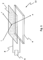
- Fig. 1 schematically shows an embodiment of a device comprising a laminated heterostructure 10.
- the laminated heterostructure 10 comprises a graphene layer 2 and a dielectric-metal compound layer 4.
- the dielectric-metal compound layer 4 may, for example, comprise doped silicon or doped aluminium.
- the graphene layer 2 and the dielectric-metal compound layer 4 have been shown separately from each other for the purposes of improved clarity of illustration. However, in practice, the graphene layer 2 and the dielectric-metal compound layer 4 are laminated together, and are therefore actually in contact with each other.
- Incident radiation, i, falling on the laminated heterostructure 10 is converted into reflected radiation, r, and absorbed radiation, a, in different relative proportions, such that the amount of reflected radiation, r, plus the amount of absorbed radiation, a, adds up to the total amount of incident radiation, i.
- the relative proportions of the reflected radiation, r, and of the absorbed radiation, a are variable and depend on the optoelectronic properties of the laminated heterostructure 10, which are tuneable.
- the device of Fig. 1 further comprises a data modulating and energy harvesting control unit 6, which is electrically connected to the laminated heterostructure 10 via circuitry 8.
- the control unit 6 is configured to alter the relative proportions in which the laminated heterostructure 10 reflects and absorbs incident radiation.
- the control unit 6 may set the relative proportions in which the laminated heterostructure 10 can reflect and absorb incident radiation to be different at different wavelengths of the incident radiation.
- the control unit 6 is also configured to select whether the laminated heterostructure 10 transmits data by optical modulation of incident radiation, harvests energy from incident radiation, reflects incident radiation, or a combination of all three.
- the reflected radiation, r can be used to transmit data by modulating a data signal supplied to the laminated heterostructure 10 by the control unit 6, whereas the absorbed radiation, a, can be harvested as energy by the control unit 6.
- the control unit 6 alters the relative proportions in which the laminated heterostructure 10 reflects and absorbs incident radiation as desired.
- the control unit 6 may alter the optoelectronic properties of the laminated heterostructure 10 to have four different modes of operation: a first mode, in which the laminated heterostructure 10 reflects visible light, a second mode, in which the laminated heterostructure 10 appears dark, a third mode, in which the laminated heterostructure 10 transmits data by optical modulation of incident radiation, and a fourth mode, in which the laminated heterostructure 10 reflects infrared radiation, for heating and insulation.
- the control unit selects one of these different modes of operation.
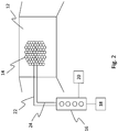
- Fig. 2 schematically shows an embodiment of an apparatus comprising a plurality of devices 14, each of which comprises a laminated heterostructure 10 comprising a graphene layer 2 and a dielectric-metal compound layer 4.
- the devices 14 are similar to each other and can be arranged in a cellular pattern on a surface.
- the devices 14 are each hexagonal in shape, so that they can be tessellated, and are integrated into a flexible membrane, which has been applied to a surface 12, such as to a wall of a building or an outer surface of a domestic appliance or electronic device.
- each of the devices 14 is shown as macroscopic, in other embodiments, they may instead be microscopic or even nanoscale devices.
- the apparatus of Fig. 2 further comprises a control unit 16, an energy harvester 18 and a data modulator 20.
- the control unit 16 is electrically connected to each of the plurality of devices 14 via a data cable 22 and an energy transfer cable 24.
- the energy harvester 18 is electrically connected to the control unit 16 to collect energy harvested by the devices 14, and the data modulator 20 is electrically connected to the control unit 16 to supply the devices 14 with a data signal which the devices 14 can modulate to transmit data.
- the control unit 16 is able to select a mode of operation of each of the devices 14 to do one or more of: transmit data supplied from the data modulator 20 using optical modulation of reflected radiation incident on the respective devices 14, harvest energy from radiation absorbed by the respective devices 14 and relay the harvested energy to the energy harvester 18, and reflect the radiation incident on the respective devices 14.
- one or more of the devices 14 may be in a different mode of operation than other ones of the devices 14. For example, most of the devices may be in a "dark" mode to provide the surface 12 with an overall visual appearance of blackness, but a small minority of the devices 14 may be in a data transmission mode to transmit a data signal or to provide a visual display.
- the apparatus can simultaneously display information and provide a dark environment in which the information is displayed.
- the present invention provides a device at least comprising a laminated heterostructure and a data modulating and energy harvesting control unit electrically connected to the laminated heterostructure.
- the laminated heterostructure comprises a graphene layer and a dielectric-metal compound layer.
- the dielectric-metal compound layer may, for example, comprise doped silicon or doped aluminium.
- the control unit is configured to alter the relative proportions in which the laminated heterostructure can reflect and absorb incident radiation by altering the optoelectronic properties of the laminated heterostructure, and to select whether the laminated heterostructure transmits data by optical modulation of incident radiation, harvests energy from incident radiation, reflects incident radiation, or a combination of all three.
- the invention also provides a method of operating a device comprising a laminated heterostructure of a graphene layer and a dielectric-metal compound layer.
- the control unit may set the relative proportions in which the laminated heterostructure can reflect and absorb incident radiation to be different at different wavelengths, and to absorb or reflect substantially all of the incident radiation in a particular waveband.
- the invention provides an apparatus comprising a plurality of devices, each comprising such a laminated heterostructure, which can be arranged in a cellular pattern on a surface, such as by inkjet printing or by being integrated into a flexible membrane.
- the surface may, for example, be a wall of a building or an outer surface of a domestic appliance or of an electronic device.
- the apparatus is able to provide the surface of whatever object it is applied to with a "smart" coating, the optoelectronic properties of which can be altered as desired to give the surface a variety of different functions.
Landscapes
- Physics & Mathematics (AREA)
- Nonlinear Science (AREA)
- General Physics & Mathematics (AREA)
- Optics & Photonics (AREA)
- Optical Modulation, Optical Deflection, Nonlinear Optics, Optical Demodulation, Optical Logic Elements (AREA)
- Electrochromic Elements, Electrophoresis, Or Variable Reflection Or Absorption Elements (AREA)
Abstract
Description
- The present invention relates to a device according to claim 1 comprising a laminated heterostructure, an apparatus according to
claim 4 comprising a plurality of laminated heterostructure devices, and a method according to claim 11 of operating a laminated heterostructure device. - It is known to use laminated heterostructures of two-dimensional materials, such as graphene, black phosphorus and transition metal dichalcogenides (TMDs), for optical modulation of electromagnetic radiation in the infrared and visible wavebands. Sun, Z., Martinez, A. & Wang, F. (2016): "Optical Modulators with Two-dimensional Layered Materials", Nature Photonics, 10(4), pp. 227-238, describes optical modulation by layered material heterostructures, in which atomically thin two-dimensional layers, such as of graphene and hexagonal boron nitride (h-BN), are prepared separately and then stacked together to form van der Waals-bonded heterostructures.
-
US 2015/1568747 describes an optical modulator including a junction formed by at least one layer of graphene which forms an electrode and a transmittance modulation layer and a dielectric layer, wherein an amount of charge accumulated in the graphene is controlled by applying voltage to the junction to control transmitted light intensity. This document also discloses the use of such a junction in an imaging device and in a display apparatus. Examples of dielectric substances for use in the dielectric layer include silicon dioxide (SiO2) and hexagonal boron nitride (h-BN). - Graphene layers have also been used in energy harvesting. For example,
WO 2012/134807 describes a solar cell comprising an n-type semiconductive graphene layer stacked on a p-type semiconductive graphene layer, andCN 104201287 A describes a perovskite-based flexible film solar cell comprising graphene electrodes. - However, such laminated heterostructure devices are application specific and cannot be employed in a wide range of different contexts. It would therefore be advantageous to provide a laminated heterostructure device having several different modes of operation, which can be used in a wide variety of different contexts.
- It is therefore an object of the invention to provide a device comprising a laminated heterostructure, an apparatus comprising a plurality of laminated heterostructure devices, and a method of operating a laminated heterostructure device.
- The object of the invention is solved by a device according to claim 1. The device at least comprises a laminated heterostructure and a data modulating and energy harvesting control unit electrically connected to the laminated heterostructure. The laminated heterostructure comprises a graphene layer and a dielectric-metal compound layer. The control unit is configured to alter the relative proportions in which the laminated heterostructure can reflect and absorb incident radiation, and to select whether the laminated heterostructure transmits data by optical modulation of incident radiation, harvests energy from incident radiation, reflects incident radiation, or a combination of all three.
- The control unit may comprise control electronics, optionally associated with software, and one or more user controls, such as buttons and/or switches. The control unit can alter the relative proportions in which the laminated heterostructure can reflect and absorb incident radiation by tuning the optoelectronic properties of the laminated heterostructure. The terms "optoelectronic" and "optical modulation" as used herein are not restricted to refer just to radiation in the visible waveband, but are also intended to refer to radiation in the infrared part of the electromagnetic spectrum.
- This solution is beneficial because such a device can be used to transmit data by optical modulation of incident radiation, to harvest energy from incident radiation and/or to reflect incident radiation at different parts of the visible and infrared wavebands by altering the relative proportions in which the laminated heterostructure can reflect and absorb incident radiation via the control unit. The device can therefore be used in a wide range of different applications, as will become apparent from the description given hereinbelow.
- Advantageous embodiments of the invention may be configured according to any claim and/or part of the following description.
- In one possible preferred embodiment, the control unit is further configured to set the relative proportions in which the laminated heterostructure can reflect and absorb incident radiation to be different at different wavelengths of the incident radiation. Thus, for example, the laminated heterostructure may be tuned to absorb a majority of the incident radiation in a narrow waveband in the visible part of the electromagnetic spectrum, but to reflect more radiation than it absorbs in other parts of the visible waveband and in the infrared parts of the electromagnetic spectrum. Other examples are also possible.
- Preferably, the dielectric-metal compound layer comprises at least one of doped silicon and doped aluminium. However, the dielectric-metal compound layer may in general comprise any semiconducting material or combination of insulating and conducting materials which together with the graphene layer are able to have their optoelectronic properties tuned as desired.
- The present invention also relates to an apparatus at least comprising a plurality of devices able to be arranged in a cellular pattern on a surface, a control unit electrically connected to each of the plurality of devices, an energy harvester electrically connected to the control unit, and a data modulator electrically connected to the control unit. Each of the devices at least comprises a laminated heterostructure of a graphene layer and a dielectric-metal compound layer. The control unit is able to alter the relative proportions in which each of the devices can reflect and absorb incident radiation. The control unit is also able to select a mode of operation of each of the devices from one or more of: transmitting data supplied from the data modulator by optical modulation of incident radiation, harvesting energy from incident radiation and relaying the harvested energy to the energy harvester, and reflecting incident radiation.
- The plurality of devices may be created by inkjet printing or spray-painting graphene onto a surface already prepared with the dielectric-metal compound layer and with appropriate electrical connections to the control unit, to the data modulator and to the energy harvester, and then exposing the surface to infrared radiation strong enough to create the laminated heterostructure. The control unit may comprise control electronics, optionally associated with software, and one or more user controls, such as buttons and/or switches. These user controls may be hardware controls or virtual controls displayed on a touch screen, for example. The data modulator may be networked to receive data remotely. The energy harvester may comprise one or more of an energy storage device, such as an electrical cell or battery or a capacitor, and an energy consuming device, such as a motor, actuator or data processor.
- This solution is beneficial because the plurality of devices can be used to cover a surface, such as a wall of a room or an outer surface of a domestic appliance or an electronic device, thereby providing the room or the appliance or device with a versatile coating which can change its optoelectronic properties for data transmission, energy harvesting and reflecting radiation as desired. For example, the data transmission mode of operation may be used to communicate status information from the domestic appliance or electronic device, either by modulation of a data signal in the visible or infrared waveband, or in the form of a visual display. In another example, the energy harvesting mode of operation may be used to supply power to the appliance or device, thereby reducing its overall power consumption. In yet another example, the radiation reflecting mode of operation may be used to provide a room with desired visible and/or thermal properties, which can be switched by means of the control unit, to suit the room to different purposes, such as a darkroom or cinema, or an incubator.
- Preferably, the control unit is electrically connected to each of the plurality of devices via separate data and energy transfer cables. The data and energy transfer cables may be laid down in tracks on the surface using conventional electronic production techniques.
- Preferably, the plurality of similar devices is arranged in a cellular pattern on a surface, and the surface comprises one of a surface of a building and an outer surface of a domestic appliance or of an electronic device. This solution is beneficial because arranging the devices in a cellular pattern on a surface allows the devices to be addressed in a systematic way and for their optoelectronic properties to be altered by the control unit in a coordinated fashion.
- In another embodiment, the surface may comprise an outer surface of a domestic appliance or of an electronic device, and the control unit is housed within the domestic appliance or electronic device. The domestic appliance may, for example, be any of a washing machine, dishwasher, oven, refrigerator or heating, ventilation and air-conditioning unit. The electronic device may, for example, be a portable electronic device, such as a mobile phone, laptop or tablet computer.
- In an alternative possible embodiment, the surface may comprise a wall, ceiling, floor or roof of a building, the control unit is mounted on, in or behind the surface, and the apparatus further comprises a remote controller configured for wireless communication with the control unit. This solution is advantageous because it allows a user to control the operation of the apparatus remotely.
- Preferably, the plurality of devices have a similar shape to each other which can be tessellated on the surface. This solution is beneficial because it allows large surfaces to be completely covered with such a plurality of devices quickly and easily.
- In one possible preferred embodiment, the plurality of devices may be integrated into a flexible membrane. This solution is beneficial because it allows the apparatus to be applied to surfaces which cannot be treated using an inkjet printing or spray-painting technique, by covering the surface with such a membrane.
- The present invention also relates to a method of operating a device comprising a laminated heterostructure of a graphene layer and a dielectric-metal compound layer, wherein the method at least comprises altering the relative proportions in which the laminated heterostructure can reflect and absorb incident radiation, and selecting whether the device transmits data by modulating the reflected radiation, harvests energy from the absorbed radiation, reflects incident radiation, or a combination of all three.
- Preferably, the method further comprises setting the relative proportions in which the laminated heterostructure can reflect and absorb incident radiation to be different at different wavelengths of the incident radiation. This solution is beneficial because it allows, for example, the optoelectronic properties of the laminated heterostructure to be made different in one part of the electromagnetic spectrum (for example, the visible waveband) from what they are in another part of the electromagnetic spectrum (for example, the infrared).
- In a further preferred embodiment, the laminated heterostructure may be tuned to absorb or reflect substantially all of the incident radiation in the visible waveband. If the laminated heterostructure is tuned to absorb substantially all of the incident radiation in the visible waveband, it will appear black. If, on the other hand, the laminated heterostructure is tuned to reflect substantially all of the incident radiation in the visible waveband, it will have a specular (mirror-like) appearance. The former, black appearance is useful, for example, if the laminated heterostructure is applied to the walls of a room to be used for screening a film, in the manner of a cinema, or for carrying out light-sensitive operations, such as developing photographic film. The latter, mirror-like appearance can be useful, for example, in other applications, such as lighting and relaying optical information.
- Alternatively or additionally, the laminated heterostructure may be tuned to absorb or reflect substantially all of the incident radiation in the infrared waveband. If the laminated heterostructure is tuned to absorb substantially all of the incident radiation in the infrared waveband, this makes the device useful for energy harvesting purposes. If, on the other hand, the laminated heterostructure is tuned to reflect substantially all of the incident radiation in the infrared waveband, this makes the device useful in heating and insulation applications, by preventing the leakage of thermal radiation through a surface on which the laminated heterostructure is applied.
- The method may further comprise modulating incident radiation reflected by the laminated heterostructure with a data signal. The data can be modulated at frequencies up to several GHz. This solution is therefore beneficial because it allows the laminated heterostructure to be used to transmit data very rapidly.
- The present invention further relates to a computer program product or a program code or system for executing one or more than one of the herein described methods.
- Further features, goals and advantages of the present invention will now be described in association with the accompanying drawings, in which exemplary components of the invention are illustrated. Components of the devices and methods according to the invention which are at least essentially equivalent to each other with respect to their function can be marked by the same reference numerals, wherein such components do not have to be marked or described in all of the drawings.
- In the following description, the invention is described by way of example only with respect to the accompanying drawings.
-
-
Fig. 1 is a schematic diagram of an embodiment of device comprising a laminated heterostructure; and -
Fig. 2 is a schematic diagram of an embodiment of an apparatus comprising a cellular membrane of the laminated heterostructure ofFig. 1 applied to a surface. -
Fig. 1 schematically shows an embodiment of a device comprising alaminated heterostructure 10. Thelaminated heterostructure 10 comprises agraphene layer 2 and a dielectric-metal compound layer 4. The dielectric-metal compound layer 4 may, for example, comprise doped silicon or doped aluminium. InFig. 1 , thegraphene layer 2 and the dielectric-metal compound layer 4 have been shown separately from each other for the purposes of improved clarity of illustration. However, in practice, thegraphene layer 2 and the dielectric-metal compound layer 4 are laminated together, and are therefore actually in contact with each other. Incident radiation, i, falling on thelaminated heterostructure 10 is converted into reflected radiation, r, and absorbed radiation, a, in different relative proportions, such that the amount of reflected radiation, r, plus the amount of absorbed radiation, a, adds up to the total amount of incident radiation, i. The relative proportions of the reflected radiation, r, and of the absorbed radiation, a, are variable and depend on the optoelectronic properties of thelaminated heterostructure 10, which are tuneable. - To this end, the device of
Fig. 1 further comprises a data modulating and energyharvesting control unit 6, which is electrically connected to thelaminated heterostructure 10 viacircuitry 8. Thecontrol unit 6 is configured to alter the relative proportions in which thelaminated heterostructure 10 reflects and absorbs incident radiation. Thecontrol unit 6 may set the relative proportions in which thelaminated heterostructure 10 can reflect and absorb incident radiation to be different at different wavelengths of the incident radiation. Thecontrol unit 6 is also configured to select whether thelaminated heterostructure 10 transmits data by optical modulation of incident radiation, harvests energy from incident radiation, reflects incident radiation, or a combination of all three. The reflected radiation, r, can be used to transmit data by modulating a data signal supplied to thelaminated heterostructure 10 by thecontrol unit 6, whereas the absorbed radiation, a, can be harvested as energy by thecontrol unit 6. - During operation, the
control unit 6 alters the relative proportions in which thelaminated heterostructure 10 reflects and absorbs incident radiation as desired. For example, thecontrol unit 6 may alter the optoelectronic properties of thelaminated heterostructure 10 to have four different modes of operation: a first mode, in which thelaminated heterostructure 10 reflects visible light, a second mode, in which thelaminated heterostructure 10 appears dark, a third mode, in which thelaminated heterostructure 10 transmits data by optical modulation of incident radiation, and a fourth mode, in which thelaminated heterostructure 10 reflects infrared radiation, for heating and insulation. The control unit then selects one of these different modes of operation. -
Fig. 2 schematically shows an embodiment of an apparatus comprising a plurality ofdevices 14, each of which comprises alaminated heterostructure 10 comprising agraphene layer 2 and a dielectric-metal compound layer 4. Thedevices 14 are similar to each other and can be arranged in a cellular pattern on a surface. In the embodiment shown inFig. 2 , thedevices 14 are each hexagonal in shape, so that they can be tessellated, and are integrated into a flexible membrane, which has been applied to asurface 12, such as to a wall of a building or an outer surface of a domestic appliance or electronic device. Whereas in the illustrated embodiment, each of thedevices 14 is shown as macroscopic, in other embodiments, they may instead be microscopic or even nanoscale devices. - The apparatus of
Fig. 2 further comprises acontrol unit 16, anenergy harvester 18 and adata modulator 20. Thecontrol unit 16 is electrically connected to each of the plurality ofdevices 14 via adata cable 22 and anenergy transfer cable 24. Theenergy harvester 18 is electrically connected to thecontrol unit 16 to collect energy harvested by thedevices 14, and thedata modulator 20 is electrically connected to thecontrol unit 16 to supply thedevices 14 with a data signal which thedevices 14 can modulate to transmit data. Thecontrol unit 16 is able to select a mode of operation of each of thedevices 14 to do one or more of: transmit data supplied from thedata modulator 20 using optical modulation of reflected radiation incident on therespective devices 14, harvest energy from radiation absorbed by therespective devices 14 and relay the harvested energy to theenergy harvester 18, and reflect the radiation incident on therespective devices 14. - During operation, one or more of the
devices 14 may be in a different mode of operation than other ones of thedevices 14. For example, most of the devices may be in a "dark" mode to provide thesurface 12 with an overall visual appearance of blackness, but a small minority of thedevices 14 may be in a data transmission mode to transmit a data signal or to provide a visual display. Thus the apparatus can simultaneously display information and provide a dark environment in which the information is displayed. - In summary, therefore, the present invention provides a device at least comprising a laminated heterostructure and a data modulating and energy harvesting control unit electrically connected to the laminated heterostructure. The laminated heterostructure comprises a graphene layer and a dielectric-metal compound layer. The dielectric-metal compound layer may, for example, comprise doped silicon or doped aluminium. The control unit is configured to alter the relative proportions in which the laminated heterostructure can reflect and absorb incident radiation by altering the optoelectronic properties of the laminated heterostructure, and to select whether the laminated heterostructure transmits data by optical modulation of incident radiation, harvests energy from incident radiation, reflects incident radiation, or a combination of all three. Thus, the invention also provides a method of operating a device comprising a laminated heterostructure of a graphene layer and a dielectric-metal compound layer. The control unit may set the relative proportions in which the laminated heterostructure can reflect and absorb incident radiation to be different at different wavelengths, and to absorb or reflect substantially all of the incident radiation in a particular waveband. Furthermore, the invention provides an apparatus comprising a plurality of devices, each comprising such a laminated heterostructure, which can be arranged in a cellular pattern on a surface, such as by inkjet printing or by being integrated into a flexible membrane. The surface may, for example, be a wall of a building or an outer surface of a domestic appliance or of an electronic device. Thus the apparatus is able to provide the surface of whatever object it is applied to with a "smart" coating, the optoelectronic properties of which can be altered as desired to give the surface a variety of different functions.
-
- 2
- Graphene layer
- 4
- Dielectric-metal compound layer
- 6
- Data modulator/energy harvester
- 8
- Interconnecting circuitry
- 10
- Laminated heterostructure
- a
- Absorbed radiation
- i
- Incident radiation
- r
- Reflected radiation
- 12
- Surface
- 14
- Cellular membrane of laminated heterostructure devices
- 16
- Control unit
- 18
- Energy harvester
- 20
- Data modulator
- 22
- Data cable
- 24
- Energy transfer cable
Claims (15)
- A device at least comprising:a laminated heterostructure (10) of a graphene layer (2) and a dielectric-metal compound layer (4); anda data modulating and energy harvesting control unit (6) electrically connected to the laminated heterostructure (10);wherein the control unit (6) is configured to alter the relative proportions in which the laminated heterostructure (10) can reflect and absorb incident radiation, and to select whether the laminated heterostructure (10) transmits data by optical modulation of incident radiation, harvests energy from incident radiation, reflects incident radiation, or a combination of all three.
- A device according to claim 1, wherein the control unit (6) is further configured to set the relative proportions in which the laminated heterostructure (10) can reflect and absorb incident radiation to be different at different wavelengths of the incident radiation.
- A device according to claim 1 or claim 2, wherein the dielectric-metal compound layer (4) comprises at least one of doped silicon and doped aluminium.
- An apparatus at least comprising:a plurality of devices (14) able to be arranged in a cellular pattern on a surface (12), wherein each device (14) at least comprises a laminated heterostructure (10) of a graphene layer (2) and a dielectric-metal compound layer (4);a control unit (16) electrically connected to each of the plurality of devices (14);an energy harvester (18) electrically connected to the control unit (16); anda data modulator (20) electrically connected to the control unit (16);wherein the control unit (16) is able to alter the relative proportions in which each of the devices (14) can reflect and absorb incident radiation and to select a mode of operation of each of the devices (14) from one or more of:transmitting data supplied from the data modulator (20) by optical modulation of incident radiation;harvesting energy from incident radiation and relaying the harvested energy to the energy harvester (18); andreflecting incident radiation.
- An apparatus according to claim 4, wherein the control unit (16) is electrically connected to each of the plurality of devices (14) via separate data (22) and energy transfer (24) cables.
- An apparatus according to claim 4 or claim 5, wherein the plurality of devices (14) is arranged in a cellular pattern on a surface (12), and the surface (12) comprises one of a surface of a building and an outer surface of a domestic appliance or of an electronic device.
- An apparatus according to claim 6, wherein the surface (12) comprises an outer surface of a domestic appliance or of an electronic device, and the control unit (16) is housed within the domestic appliance or electronic device.
- An apparatus according to claim 6, wherein the surface (12) comprises a wall, ceiling, floor or roof of a building, the control unit (16) is mounted on, in or behind the surface, and the apparatus further comprises a remote controller configured for wireless communication with the control unit (16).
- An apparatus according to any one of claims 4 to 8, wherein the plurality of devices (14) have a similar shape to each other which can be tessellated on the surface (12).
- An apparatus according to any one of claims 4 to 9, wherein the plurality of devices (14) are integrated into a flexible membrane.
- A method of operating a device comprising a laminated heterostructure (10) of a graphene layer (2) and a dielectric-metal compound layer (4), the method at least comprising:altering the relative proportions in which the laminated heterostructure (10) can reflect and absorb incident radiation; andselecting whether the device transmits data by modulating the reflected radiation, harvests energy from the absorbed radiation, reflects incident radiation, or a combination of all three.
- A method according to claim 11, further comprising setting the relative proportions in which the laminated heterostructure (10) can reflect and absorb incident radiation to be different at different wavelengths of the incident radiation.
- A method according to claim 11 or claim 12, comprising tuning the laminated heterostructure (10) to absorb or reflect substantially all of the incident radiation in the visible waveband.
- A method according to any one of claims 11 to 13, comprising tuning the laminated heterostructure (10) to absorb or reflect substantially all of the incident radiation in the infrared waveband.
- A method according to any one of claims 11 to 14, comprising modulating incident radiation reflected by the laminated heterostructure (10) with a data signal.
Priority Applications (1)
| Application Number | Priority Date | Filing Date | Title |
|---|---|---|---|
| EP17172204.4A EP3407121B1 (en) | 2017-05-22 | 2017-05-22 | Laminated heterostructure device, apparatus comprising the same, and method of operating a laminated heterostructure device |
Applications Claiming Priority (1)
| Application Number | Priority Date | Filing Date | Title |
|---|---|---|---|
| EP17172204.4A EP3407121B1 (en) | 2017-05-22 | 2017-05-22 | Laminated heterostructure device, apparatus comprising the same, and method of operating a laminated heterostructure device |
Publications (2)
| Publication Number | Publication Date |
|---|---|
| EP3407121A1 true EP3407121A1 (en) | 2018-11-28 |
| EP3407121B1 EP3407121B1 (en) | 2021-09-08 |
Family
ID=58800645
Family Applications (1)
| Application Number | Title | Priority Date | Filing Date |
|---|---|---|---|
| EP17172204.4A Active EP3407121B1 (en) | 2017-05-22 | 2017-05-22 | Laminated heterostructure device, apparatus comprising the same, and method of operating a laminated heterostructure device |
Country Status (1)
| Country | Link |
|---|---|
| EP (1) | EP3407121B1 (en) |
Citations (6)
| Publication number | Priority date | Publication date | Assignee | Title |
|---|---|---|---|---|
| WO2012134807A2 (en) | 2011-03-29 | 2012-10-04 | California Institute Of Technology | Graphene-based multi-junctions flexible solar cell |
| CN104201287A (en) | 2014-08-27 | 2014-12-10 | 湖南省天赐阳光太阳能有限责任公司 | Perovskite based flexible film solar cell and preparation method thereof |
| US20150083206A1 (en) * | 2012-03-22 | 2015-03-26 | The University Of Manchester | Photovoltaic cells |
| US20150168747A1 (en) | 2012-06-14 | 2015-06-18 | Sony Corporation | Optical modulator, imaging device and display apparatus |
| WO2015130189A1 (en) * | 2014-02-28 | 2015-09-03 | Nokia Technologies Oy | Method and apparatus for oxidation of two-dimensional materials |
| US20150332920A1 (en) * | 2014-05-19 | 2015-11-19 | Research & Business Foundation Sungkyunkwan University | Electronic device having graphene-semiconductor multi-junction and method of manufacturing the electronic device |
-
2017
- 2017-05-22 EP EP17172204.4A patent/EP3407121B1/en active Active
Patent Citations (6)
| Publication number | Priority date | Publication date | Assignee | Title |
|---|---|---|---|---|
| WO2012134807A2 (en) | 2011-03-29 | 2012-10-04 | California Institute Of Technology | Graphene-based multi-junctions flexible solar cell |
| US20150083206A1 (en) * | 2012-03-22 | 2015-03-26 | The University Of Manchester | Photovoltaic cells |
| US20150168747A1 (en) | 2012-06-14 | 2015-06-18 | Sony Corporation | Optical modulator, imaging device and display apparatus |
| WO2015130189A1 (en) * | 2014-02-28 | 2015-09-03 | Nokia Technologies Oy | Method and apparatus for oxidation of two-dimensional materials |
| US20150332920A1 (en) * | 2014-05-19 | 2015-11-19 | Research & Business Foundation Sungkyunkwan University | Electronic device having graphene-semiconductor multi-junction and method of manufacturing the electronic device |
| CN104201287A (en) | 2014-08-27 | 2014-12-10 | 湖南省天赐阳光太阳能有限责任公司 | Perovskite based flexible film solar cell and preparation method thereof |
Non-Patent Citations (2)
| Title |
|---|
| LINDER JACOB ET AL: "Dynamical tuning between nearly perfect reflection, absorption, and transmission of light via graphene/dielectric structures", SCIENTIFIC REPORTS, vol. 6, no. 1, 1 December 2016 (2016-12-01), XP055781986, Retrieved from the Internet <URL:http://www.nature.com/articles/srep38141> DOI: 10.1038/srep38141 * |
| SUN, Z.; MARTINEZ, A; WANG, F.: "Optical Modulators with Two-dimensional Layered Materials", NATURE PHOTONICS, vol. 10, no. 4, 2016, pages 227 - 238 |
Also Published As
| Publication number | Publication date |
|---|---|
| EP3407121B1 (en) | 2021-09-08 |
Similar Documents
| Publication | Publication Date | Title |
|---|---|---|
| Katz et al. | Opportunities and challenges for visible light communications in 6G | |
| TWI778907B (en) | Apparatus, method, and non-transitory computer readable media for controlling optically switchable windows | |
| TWI702754B (en) | Window antennas | |
| US10770436B2 (en) | Light-emitting diode (LED) device | |
| US9986622B2 (en) | Lighting system, lighting apparastus, and lighting control method | |
| EP3223532B1 (en) | Applications for controlling optically switchable devices | |
| JP2022037171A (en) | A method for controlling at least one colorable window, a device for controlling at least one colorable window, and a system for controlling at least one colorable window. | |
| CN113940014A (en) | Antenna system for controlled coverage in buildings | |
| US10841166B2 (en) | Commissioning and personalizing devices in a local area network | |
| JPWO2017175796A1 (en) | Dimming module | |
| JP2019504372A (en) | Smart clothing, user terminal, system including the same, and smart clothing design changing method | |
| JP7706461B2 (en) | Facility Data and Power Networks | |
| AU2016262457A1 (en) | Solar power generation, distribution, and communication system | |
| EP3407121B1 (en) | Laminated heterostructure device, apparatus comprising the same, and method of operating a laminated heterostructure device | |
| US9547212B2 (en) | Electrochromic device comprising an integrated heating system | |
| CN121399537A (en) | Data and power network of facilities | |
| KR101980259B1 (en) | Smart window for performing locking and operating | |
| CN207504913U (en) | Data transmission system and stage lighting system | |
| CN219349727U (en) | Highlight display screen for unmanned aerial vehicle | |
| CN206402493U (en) | A kind of wireless inter-controlled switch of feedback-type and wireless control system controlled based on mirror image | |
| KR102418001B1 (en) | Roll screen type solar photovoltaic power ganerating apparatus | |
| US20250200236A1 (en) | Electronic device and method for operating the same | |
| EP4429405A1 (en) | A heating device | |
| CN113839467B (en) | Wireless energy conversion device and wireless energy conversion system | |
| HK1242094B (en) | Applications for controlling optically switchable devices |
Legal Events
| Date | Code | Title | Description |
|---|---|---|---|
| PUAI | Public reference made under article 153(3) epc to a published international application that has entered the european phase |
Free format text: ORIGINAL CODE: 0009012 |
|
| STAA | Information on the status of an ep patent application or granted ep patent |
Free format text: STATUS: THE APPLICATION HAS BEEN PUBLISHED |
|
| AK | Designated contracting states |
Kind code of ref document: A1 Designated state(s): AL AT BE BG CH CY CZ DE DK EE ES FI FR GB GR HR HU IE IS IT LI LT LU LV MC MK MT NL NO PL PT RO RS SE SI SK SM TR |
|
| AX | Request for extension of the european patent |
Extension state: BA ME |
|
| STAA | Information on the status of an ep patent application or granted ep patent |
Free format text: STATUS: REQUEST FOR EXAMINATION WAS MADE |
|
| 17P | Request for examination filed |
Effective date: 20190520 |
|
| RBV | Designated contracting states (corrected) |
Designated state(s): AL AT BE BG CH CY CZ DE DK EE ES FI FR GB GR HR HU IE IS IT LI LT LU LV MC MK MT NL NO PL PT RO RS SE SI SK SM TR |
|
| GRAP | Despatch of communication of intention to grant a patent |
Free format text: ORIGINAL CODE: EPIDOSNIGR1 |
|
| STAA | Information on the status of an ep patent application or granted ep patent |
Free format text: STATUS: GRANT OF PATENT IS INTENDED |
|
| INTG | Intention to grant announced |
Effective date: 20210329 |
|
| GRAS | Grant fee paid |
Free format text: ORIGINAL CODE: EPIDOSNIGR3 |
|
| GRAA | (expected) grant |
Free format text: ORIGINAL CODE: 0009210 |
|
| STAA | Information on the status of an ep patent application or granted ep patent |
Free format text: STATUS: THE PATENT HAS BEEN GRANTED |
|
| AK | Designated contracting states |
Kind code of ref document: B1 Designated state(s): AL AT BE BG CH CY CZ DE DK EE ES FI FR GB GR HR HU IE IS IT LI LT LU LV MC MK MT NL NO PL PT RO RS SE SI SK SM TR |
|
| REG | Reference to a national code |
Ref country code: GB Ref legal event code: FG4D |
|
| REG | Reference to a national code |
Ref country code: AT Ref legal event code: REF Ref document number: 1429090 Country of ref document: AT Kind code of ref document: T Effective date: 20210915 Ref country code: CH Ref legal event code: EP |
|
| REG | Reference to a national code |
Ref country code: IE Ref legal event code: FG4D |
|
| REG | Reference to a national code |
Ref country code: DE Ref legal event code: R096 Ref document number: 602017045548 Country of ref document: DE |
|
| REG | Reference to a national code |
Ref country code: LT Ref legal event code: MG9D |
|
| REG | Reference to a national code |
Ref country code: NL Ref legal event code: MP Effective date: 20210908 |
|
| PG25 | Lapsed in a contracting state [announced via postgrant information from national office to epo] |
Ref country code: RS Free format text: LAPSE BECAUSE OF FAILURE TO SUBMIT A TRANSLATION OF THE DESCRIPTION OR TO PAY THE FEE WITHIN THE PRESCRIBED TIME-LIMIT Effective date: 20210908 Ref country code: SE Free format text: LAPSE BECAUSE OF FAILURE TO SUBMIT A TRANSLATION OF THE DESCRIPTION OR TO PAY THE FEE WITHIN THE PRESCRIBED TIME-LIMIT Effective date: 20210908 Ref country code: NO Free format text: LAPSE BECAUSE OF FAILURE TO SUBMIT A TRANSLATION OF THE DESCRIPTION OR TO PAY THE FEE WITHIN THE PRESCRIBED TIME-LIMIT Effective date: 20211208 Ref country code: HR Free format text: LAPSE BECAUSE OF FAILURE TO SUBMIT A TRANSLATION OF THE DESCRIPTION OR TO PAY THE FEE WITHIN THE PRESCRIBED TIME-LIMIT Effective date: 20210908 Ref country code: FI Free format text: LAPSE BECAUSE OF FAILURE TO SUBMIT A TRANSLATION OF THE DESCRIPTION OR TO PAY THE FEE WITHIN THE PRESCRIBED TIME-LIMIT Effective date: 20210908 Ref country code: ES Free format text: LAPSE BECAUSE OF FAILURE TO SUBMIT A TRANSLATION OF THE DESCRIPTION OR TO PAY THE FEE WITHIN THE PRESCRIBED TIME-LIMIT Effective date: 20210908 Ref country code: LT Free format text: LAPSE BECAUSE OF FAILURE TO SUBMIT A TRANSLATION OF THE DESCRIPTION OR TO PAY THE FEE WITHIN THE PRESCRIBED TIME-LIMIT Effective date: 20210908 Ref country code: BG Free format text: LAPSE BECAUSE OF FAILURE TO SUBMIT A TRANSLATION OF THE DESCRIPTION OR TO PAY THE FEE WITHIN THE PRESCRIBED TIME-LIMIT Effective date: 20211208 |
|
| REG | Reference to a national code |
Ref country code: AT Ref legal event code: MK05 Ref document number: 1429090 Country of ref document: AT Kind code of ref document: T Effective date: 20210908 |
|
| PG25 | Lapsed in a contracting state [announced via postgrant information from national office to epo] |
Ref country code: LV Free format text: LAPSE BECAUSE OF FAILURE TO SUBMIT A TRANSLATION OF THE DESCRIPTION OR TO PAY THE FEE WITHIN THE PRESCRIBED TIME-LIMIT Effective date: 20210908 Ref country code: GR Free format text: LAPSE BECAUSE OF FAILURE TO SUBMIT A TRANSLATION OF THE DESCRIPTION OR TO PAY THE FEE WITHIN THE PRESCRIBED TIME-LIMIT Effective date: 20211209 |
|
| PG25 | Lapsed in a contracting state [announced via postgrant information from national office to epo] |
Ref country code: AT Free format text: LAPSE BECAUSE OF FAILURE TO SUBMIT A TRANSLATION OF THE DESCRIPTION OR TO PAY THE FEE WITHIN THE PRESCRIBED TIME-LIMIT Effective date: 20210908 |
|
| PG25 | Lapsed in a contracting state [announced via postgrant information from national office to epo] |
Ref country code: IS Free format text: LAPSE BECAUSE OF FAILURE TO SUBMIT A TRANSLATION OF THE DESCRIPTION OR TO PAY THE FEE WITHIN THE PRESCRIBED TIME-LIMIT Effective date: 20220108 Ref country code: SM Free format text: LAPSE BECAUSE OF FAILURE TO SUBMIT A TRANSLATION OF THE DESCRIPTION OR TO PAY THE FEE WITHIN THE PRESCRIBED TIME-LIMIT Effective date: 20210908 Ref country code: SK Free format text: LAPSE BECAUSE OF FAILURE TO SUBMIT A TRANSLATION OF THE DESCRIPTION OR TO PAY THE FEE WITHIN THE PRESCRIBED TIME-LIMIT Effective date: 20210908 Ref country code: RO Free format text: LAPSE BECAUSE OF FAILURE TO SUBMIT A TRANSLATION OF THE DESCRIPTION OR TO PAY THE FEE WITHIN THE PRESCRIBED TIME-LIMIT Effective date: 20210908 Ref country code: PT Free format text: LAPSE BECAUSE OF FAILURE TO SUBMIT A TRANSLATION OF THE DESCRIPTION OR TO PAY THE FEE WITHIN THE PRESCRIBED TIME-LIMIT Effective date: 20220110 Ref country code: PL Free format text: LAPSE BECAUSE OF FAILURE TO SUBMIT A TRANSLATION OF THE DESCRIPTION OR TO PAY THE FEE WITHIN THE PRESCRIBED TIME-LIMIT Effective date: 20210908 Ref country code: NL Free format text: LAPSE BECAUSE OF FAILURE TO SUBMIT A TRANSLATION OF THE DESCRIPTION OR TO PAY THE FEE WITHIN THE PRESCRIBED TIME-LIMIT Effective date: 20210908 Ref country code: EE Free format text: LAPSE BECAUSE OF FAILURE TO SUBMIT A TRANSLATION OF THE DESCRIPTION OR TO PAY THE FEE WITHIN THE PRESCRIBED TIME-LIMIT Effective date: 20210908 Ref country code: CZ Free format text: LAPSE BECAUSE OF FAILURE TO SUBMIT A TRANSLATION OF THE DESCRIPTION OR TO PAY THE FEE WITHIN THE PRESCRIBED TIME-LIMIT Effective date: 20210908 Ref country code: AL Free format text: LAPSE BECAUSE OF FAILURE TO SUBMIT A TRANSLATION OF THE DESCRIPTION OR TO PAY THE FEE WITHIN THE PRESCRIBED TIME-LIMIT Effective date: 20210908 |
|
| REG | Reference to a national code |
Ref country code: DE Ref legal event code: R097 Ref document number: 602017045548 Country of ref document: DE |
|
| PLBE | No opposition filed within time limit |
Free format text: ORIGINAL CODE: 0009261 |
|
| STAA | Information on the status of an ep patent application or granted ep patent |
Free format text: STATUS: NO OPPOSITION FILED WITHIN TIME LIMIT |
|
| PG25 | Lapsed in a contracting state [announced via postgrant information from national office to epo] |
Ref country code: DK Free format text: LAPSE BECAUSE OF FAILURE TO SUBMIT A TRANSLATION OF THE DESCRIPTION OR TO PAY THE FEE WITHIN THE PRESCRIBED TIME-LIMIT Effective date: 20210908 |
|
| 26N | No opposition filed |
Effective date: 20220609 |
|
| PG25 | Lapsed in a contracting state [announced via postgrant information from national office to epo] |
Ref country code: SI Free format text: LAPSE BECAUSE OF FAILURE TO SUBMIT A TRANSLATION OF THE DESCRIPTION OR TO PAY THE FEE WITHIN THE PRESCRIBED TIME-LIMIT Effective date: 20210908 |
|
| REG | Reference to a national code |
Ref country code: CH Ref legal event code: PL |
|
| REG | Reference to a national code |
Ref country code: BE Ref legal event code: MM Effective date: 20220531 |
|
| PG25 | Lapsed in a contracting state [announced via postgrant information from national office to epo] |
Ref country code: MC Free format text: LAPSE BECAUSE OF FAILURE TO SUBMIT A TRANSLATION OF THE DESCRIPTION OR TO PAY THE FEE WITHIN THE PRESCRIBED TIME-LIMIT Effective date: 20210908 Ref country code: LU Free format text: LAPSE BECAUSE OF NON-PAYMENT OF DUE FEES Effective date: 20220522 Ref country code: LI Free format text: LAPSE BECAUSE OF NON-PAYMENT OF DUE FEES Effective date: 20220531 Ref country code: IT Free format text: LAPSE BECAUSE OF FAILURE TO SUBMIT A TRANSLATION OF THE DESCRIPTION OR TO PAY THE FEE WITHIN THE PRESCRIBED TIME-LIMIT Effective date: 20210908 Ref country code: CH Free format text: LAPSE BECAUSE OF NON-PAYMENT OF DUE FEES Effective date: 20220531 |
|
| PG25 | Lapsed in a contracting state [announced via postgrant information from national office to epo] |
Ref country code: IE Free format text: LAPSE BECAUSE OF NON-PAYMENT OF DUE FEES Effective date: 20220522 Ref country code: FR Free format text: LAPSE BECAUSE OF NON-PAYMENT OF DUE FEES Effective date: 20220531 |
|
| PG25 | Lapsed in a contracting state [announced via postgrant information from national office to epo] |
Ref country code: BE Free format text: LAPSE BECAUSE OF NON-PAYMENT OF DUE FEES Effective date: 20220531 |
|
| PGFP | Annual fee paid to national office [announced via postgrant information from national office to epo] |
Ref country code: GB Payment date: 20230920 Year of fee payment: 7 |
|
| PGFP | Annual fee paid to national office [announced via postgrant information from national office to epo] |
Ref country code: DE Payment date: 20230920 Year of fee payment: 7 |
|
| PG25 | Lapsed in a contracting state [announced via postgrant information from national office to epo] |
Ref country code: HU Free format text: LAPSE BECAUSE OF FAILURE TO SUBMIT A TRANSLATION OF THE DESCRIPTION OR TO PAY THE FEE WITHIN THE PRESCRIBED TIME-LIMIT; INVALID AB INITIO Effective date: 20170522 |
|
| PG25 | Lapsed in a contracting state [announced via postgrant information from national office to epo] |
Ref country code: MK Free format text: LAPSE BECAUSE OF FAILURE TO SUBMIT A TRANSLATION OF THE DESCRIPTION OR TO PAY THE FEE WITHIN THE PRESCRIBED TIME-LIMIT Effective date: 20210908 Ref country code: CY Free format text: LAPSE BECAUSE OF FAILURE TO SUBMIT A TRANSLATION OF THE DESCRIPTION OR TO PAY THE FEE WITHIN THE PRESCRIBED TIME-LIMIT Effective date: 20210908 |
|
| PG25 | Lapsed in a contracting state [announced via postgrant information from national office to epo] |
Ref country code: MT Free format text: LAPSE BECAUSE OF FAILURE TO SUBMIT A TRANSLATION OF THE DESCRIPTION OR TO PAY THE FEE WITHIN THE PRESCRIBED TIME-LIMIT Effective date: 20210908 |
|
| REG | Reference to a national code |
Ref country code: DE Ref legal event code: R119 Ref document number: 602017045548 Country of ref document: DE |
|
| GBPC | Gb: european patent ceased through non-payment of renewal fee |
Effective date: 20240522 |
|
| PG25 | Lapsed in a contracting state [announced via postgrant information from national office to epo] |
Ref country code: DE Free format text: LAPSE BECAUSE OF NON-PAYMENT OF DUE FEES Effective date: 20241203 |
|
| PG25 | Lapsed in a contracting state [announced via postgrant information from national office to epo] |
Ref country code: GB Free format text: LAPSE BECAUSE OF NON-PAYMENT OF DUE FEES Effective date: 20240522 |
|
| PGFP | Annual fee paid to national office [announced via postgrant information from national office to epo] |
Ref country code: TR Payment date: 20260522 Year of fee payment: 10 |