EP3405330B1 - Creating homogeneous optical elements by additive manufacturing - Google Patents
Creating homogeneous optical elements by additive manufacturing Download PDFInfo
- Publication number
- EP3405330B1 EP3405330B1 EP17741799.5A EP17741799A EP3405330B1 EP 3405330 B1 EP3405330 B1 EP 3405330B1 EP 17741799 A EP17741799 A EP 17741799A EP 3405330 B1 EP3405330 B1 EP 3405330B1
- Authority
- EP
- European Patent Office
- Prior art keywords
- light
- diffuser
- optical element
- resin
- light source
- Prior art date
- Legal status (The legal status is an assumption and is not a legal conclusion. Google has not performed a legal analysis and makes no representation as to the accuracy of the status listed.)
- Active
Links
Images





Classifications
-
- B—PERFORMING OPERATIONS; TRANSPORTING
- B29—WORKING OF PLASTICS; WORKING OF SUBSTANCES IN A PLASTIC STATE IN GENERAL
- B29D—PRODUCING PARTICULAR ARTICLES FROM PLASTICS OR FROM SUBSTANCES IN A PLASTIC STATE
- B29D11/00—Producing optical elements, e.g. lenses or prisms
- B29D11/00009—Production of simple or compound lenses
-
- B—PERFORMING OPERATIONS; TRANSPORTING
- B29—WORKING OF PLASTICS; WORKING OF SUBSTANCES IN A PLASTIC STATE IN GENERAL
- B29C—SHAPING OR JOINING OF PLASTICS; SHAPING OF MATERIAL IN A PLASTIC STATE, NOT OTHERWISE PROVIDED FOR; AFTER-TREATMENT OF THE SHAPED PRODUCTS, e.g. REPAIRING
- B29C64/00—Additive manufacturing, i.e. manufacturing of three-dimensional [3D] objects by additive deposition, additive agglomeration or additive layering, e.g. by 3D printing, stereolithography or selective laser sintering
- B29C64/10—Processes of additive manufacturing
- B29C64/106—Processes of additive manufacturing using only liquids or viscous materials, e.g. depositing a continuous bead of viscous material
- B29C64/124—Processes of additive manufacturing using only liquids or viscous materials, e.g. depositing a continuous bead of viscous material using layers of liquid which are selectively solidified
- B29C64/129—Processes of additive manufacturing using only liquids or viscous materials, e.g. depositing a continuous bead of viscous material using layers of liquid which are selectively solidified characterised by the energy source therefor, e.g. by global irradiation combined with a mask
- B29C64/135—Processes of additive manufacturing using only liquids or viscous materials, e.g. depositing a continuous bead of viscous material using layers of liquid which are selectively solidified characterised by the energy source therefor, e.g. by global irradiation combined with a mask the energy source being concentrated, e.g. scanning lasers or focused light sources
-
- B—PERFORMING OPERATIONS; TRANSPORTING
- B29—WORKING OF PLASTICS; WORKING OF SUBSTANCES IN A PLASTIC STATE IN GENERAL
- B29C—SHAPING OR JOINING OF PLASTICS; SHAPING OF MATERIAL IN A PLASTIC STATE, NOT OTHERWISE PROVIDED FOR; AFTER-TREATMENT OF THE SHAPED PRODUCTS, e.g. REPAIRING
- B29C64/00—Additive manufacturing, i.e. manufacturing of three-dimensional [3D] objects by additive deposition, additive agglomeration or additive layering, e.g. by 3D printing, stereolithography or selective laser sintering
- B29C64/20—Apparatus for additive manufacturing; Details thereof or accessories therefor
- B29C64/264—Arrangements for irradiation
-
- B—PERFORMING OPERATIONS; TRANSPORTING
- B29—WORKING OF PLASTICS; WORKING OF SUBSTANCES IN A PLASTIC STATE IN GENERAL
- B29D—PRODUCING PARTICULAR ARTICLES FROM PLASTICS OR FROM SUBSTANCES IN A PLASTIC STATE
- B29D11/00—Producing optical elements, e.g. lenses or prisms
- B29D11/00009—Production of simple or compound lenses
- B29D11/00432—Auxiliary operations, e.g. machines for filling the moulds
-
- G—PHYSICS
- G02—OPTICS
- G02B—OPTICAL ELEMENTS, SYSTEMS OR APPARATUS
- G02B1/00—Optical elements characterised by the material of which they are made; Optical coatings for optical elements
- G02B1/10—Optical coatings produced by application to, or surface treatment of, optical elements
-
- G—PHYSICS
- G02—OPTICS
- G02B—OPTICAL ELEMENTS, SYSTEMS OR APPARATUS
- G02B1/00—Optical elements characterised by the material of which they are made; Optical coatings for optical elements
- G02B1/10—Optical coatings produced by application to, or surface treatment of, optical elements
- G02B1/12—Optical coatings produced by application to, or surface treatment of, optical elements by surface treatment, e.g. by irradiation
-
- G—PHYSICS
- G02—OPTICS
- G02B—OPTICAL ELEMENTS, SYSTEMS OR APPARATUS
- G02B5/00—Optical elements other than lenses
- G02B5/02—Diffusing elements; Afocal elements
- G02B5/0205—Diffusing elements; Afocal elements characterised by the diffusing properties
- G02B5/0252—Diffusing elements; Afocal elements characterised by the diffusing properties using holographic or diffractive means
-
- B—PERFORMING OPERATIONS; TRANSPORTING
- B29—WORKING OF PLASTICS; WORKING OF SUBSTANCES IN A PLASTIC STATE IN GENERAL
- B29K—INDEXING SCHEME ASSOCIATED WITH SUBCLASSES B29B, B29C OR B29D, RELATING TO MOULDING MATERIALS OR TO MATERIALS FOR MOULDS, REINFORCEMENTS, FILLERS OR PREFORMED PARTS, e.g. INSERTS
- B29K2105/00—Condition, form or state of moulded material or of the material to be shaped
- B29K2105/0058—Liquid or visquous
-
- B—PERFORMING OPERATIONS; TRANSPORTING
- B29—WORKING OF PLASTICS; WORKING OF SUBSTANCES IN A PLASTIC STATE IN GENERAL
- B29L—INDEXING SCHEME ASSOCIATED WITH SUBCLASS B29C, RELATING TO PARTICULAR ARTICLES
- B29L2011/00—Optical elements, e.g. lenses, prisms
- B29L2011/0016—Lenses
-
- B—PERFORMING OPERATIONS; TRANSPORTING
- B33—ADDITIVE MANUFACTURING TECHNOLOGY
- B33Y—ADDITIVE MANUFACTURING, i.e. MANUFACTURING OF THREE-DIMENSIONAL [3D] OBJECTS BY ADDITIVE DEPOSITION, ADDITIVE AGGLOMERATION OR ADDITIVE LAYERING, e.g. BY 3D PRINTING, STEREOLITHOGRAPHY OR SELECTIVE LASER SINTERING
- B33Y10/00—Processes of additive manufacturing
-
- B—PERFORMING OPERATIONS; TRANSPORTING
- B33—ADDITIVE MANUFACTURING TECHNOLOGY
- B33Y—ADDITIVE MANUFACTURING, i.e. MANUFACTURING OF THREE-DIMENSIONAL [3D] OBJECTS BY ADDITIVE DEPOSITION, ADDITIVE AGGLOMERATION OR ADDITIVE LAYERING, e.g. BY 3D PRINTING, STEREOLITHOGRAPHY OR SELECTIVE LASER SINTERING
- B33Y30/00—Apparatus for additive manufacturing; Details thereof or accessories therefor
-
- B—PERFORMING OPERATIONS; TRANSPORTING
- B33—ADDITIVE MANUFACTURING TECHNOLOGY
- B33Y—ADDITIVE MANUFACTURING, i.e. MANUFACTURING OF THREE-DIMENSIONAL [3D] OBJECTS BY ADDITIVE DEPOSITION, ADDITIVE AGGLOMERATION OR ADDITIVE LAYERING, e.g. BY 3D PRINTING, STEREOLITHOGRAPHY OR SELECTIVE LASER SINTERING
- B33Y80/00—Products made by additive manufacturing
Definitions
- This disclosure relates to the making of ophthalmic elements and in particular to methods of improving the quality of eyewear lenses made by using additive techniques, and the products obtained therefrom.
- Prescription eyewear lenses are used to correct refractive errors of human vision. Eyewear lenses may be used for protection, namely to protect the eyes from excess light or from a mechanical, chemical or biological hazard.
- One shaping technology is molding. With molding, a reference surface is made in glass or other material, and the reference surface is replicated on the eyewear lens by mold casting or injection molding.
- the other shaping technology is grinding and polishing, where a solid piece of optical material is mechanically ground (or milled) and polished until the required surface is obtained.
- Prescription eyewear lenses are characterized by the large number of possible different lenses that can be potentially made. Lenses can be different in regard to lens material, modifiers embedded in the lens, coatings, power and power distribution. As refractive errors are measured in steps of 0.25 D, which is considered to be the distinguishable average threshold for human blur perception, there is a limit to the number of different optical powers that could be potentially used. Nevertheless, modern digital lenses available since around 2000 may be tailored to the user's characteristics or needs, taking into account the actual position of the lens with respect to the eye. As a consequence, the optimization of the optical performance of the eyewear lens for each individual requires the capacity of producing lenses with a large variety of optical powers.
- multifocal eyewear lenses used primarily for presbyope individuals have a continuous variation of power across the lens aperture, allowing the user to sharply focus at different distances.
- the number of different power distributions in these multifocal lenses is virtually infinite.
- Modern digital grinding (milling) and polishing technology may be used to produce arbitrary surfaces. In this way it is well suited for making eyewear lenses with the required shape variability.
- mechanical grinding and polishing is a subtractive process that requires complex and expensive machinery to guarantee the accuracy level required for eyewear products.
- Mechanical grinding and polishing requires expensive tooling and equipment for proper alignment, and uses expensive consumables including cutting tools, polishing slurries, polishing pads, and coolants. Plus, mechanical grinding and polishing is an energy consuming process that also produces a lot of waste, which is difficult to handle and eliminate.
- Molding is not a subtractive method, but it requires the previous manufacturing of the mold itself.
- the number of required lens surfaces is too numerous, molding becomes unpractical because the number of lens surfaces molded (or cast) from each mold are too low in number, resulting in a large number of molds that must be produced and kept on hand.
- a lens element has two polished surfaces, and its optical power can be distributed between the two surfaces.
- One of the surfaces can be normalized to a relatively small number of different shapes, which are made by molding, and the other surface is ground/polished to a shape required to obtain the desired optical power and optical power distribution.
- This way, the manufacturing of eyewear lenses is split in a two-step process.
- semi-finished lens blanks are produced by casting or injection molding.
- a lens manufacturer buys and stores these blanks, or produces the blanks.
- eyewear lenses make them ideal products for a more distributed and simple manufacturing process.
- An improved additive process for eyewear lens preparation would be beneficial.
- the lenses could be made on demand which has multiple benefits.
- Custom manufacturing lenses using an additive process removes the need to produce and store semi-finished blanks, eliminates material waste inherent in grinding, and reduces energy consumption by simplifying the overall process.
- additive manufacturing allows for adding or embedding structures for upcoming technologies inside the lens including using mirrors, prisms, micro-lenses, diffraction gratings, light sources, and other techniques.
- US 2015/277146 A1 discloses a method for additive manufacturing an optical element formed of layers.
- Optical elements such as lenses or spectacle lenses
- Stereo lithography (SLA) 3D printers are one such method.
- SLA printers can be adapted to different growing strategies, can be used on top of different growing platforms and/or substrates, and are fast.
- Manufacturing of spectacle lenses by additive processes provides some advantages for lens manufacturers, eye care practitioners and final customers (i.e., the lens user). Lens manufacturers may make lenses from scratch, without the need to buy and stock any blanks. Also, the additive manufacturing method is more environmentally friendly, as little or no waste is generated. Plus, making lenses by additive processes requires less energy than traditional techniques.
- SLA printers create objects as a set of 3D pixels, also called voxels.
- the 3D objects made from those voxels may not be homogenous.
- Physical and chemical properties of the material may change across the interfaces between voxels.
- local density and refractive index can be two of the physical properties that change across the interfaces between voxels.
- the optical effect of these changes in the lens material, once the lens is grown in the SLA printer, is that light scatters and diffracts as it goes through the 3D printed lens, decreasing its optical performance.
- SLA printing generally consists of shining ultra-violet (UV) light (e.g., with a wavelength of between 350nm and 420nm) in a very controlled way on a liquid resin contained in a tank.
- UV light causes the resin to polymerize and turn into a solid.
- the desired object has a digital representation which is sliced into many layers.
- Each solid layer can be created on a previous solid layer by the polymerization of a liquid polymer layer through exposure to a pattern or image of UV light, e.g., from a scanning UV laser or a digital light processing (DLP) projector.
- the UV light shined on the resin is highly directional, and voxel structures are created on the polymer layer due to the pixels on the DLP projector image or lines made by the scanning laser.
- a scanning laser SLA system includes a liquid resin 106 is inside a tank 102, and a support 104 to support an optical element 108 is immersed in the resin 106.
- the term optical element includes lenses and spectacle lenses.
- any defect 114 such as a dust spot or bubble, on the surface of or in the resin can create a tube-like shadow along the direction of the impinging laser beam 112, causing a variation in irradiance and polymerization rate.
- the irradiance along this shadow may considerably differ from the irradiance at other points.
- the variation in polymerization rate can result in a non-homogeneous optical element 108 with defects 116, shown in FIG. 1C .
- the photographic microscope image of FIG. 2 shows a non-homogeneous optical element manufactured by a scanning laser SLA system, such as shown in FIGs. 1A and 1B .
- the defects 116 in the optical element resulting from the defects 114 in the resin 106 can have a linear shape oriented along the direction of the incoming light, but can be randomly distributed across the layers.
- horizontal dark lines 210 are the boundaries between layers, and vertical lines are variations of refractive index along the growing direction, caused by local variations of irradiance of the incoming light.
- micro-bubbles 214 created the tube-like structures 216.
- other vertical lines were created by other defects not necessarily contained in the field of the photographic microscope image.
- the refractive index of the optical element 108 can vary, causing scatter light and inhibiting optical quality.
- FIG. 3 shows a light beam 320 traveling through a non-homogeneous optical element 308 manufactured by the system of FIGs. 1A , 1B , and 1C .
- the light beam 320 impinges on the non-homogeneous optical element 308 with defects 316, e.g., variations in refractive index, the light beam 320 can be scattered, e.g., conically scattered 322, in an undesired manner as it passes through the optical element 308.
- the overlapping of scanning lines 120 can produce some variation of irradiance. Since perfect matching of irradiance along consecutive scans is difficult or impossible, scanning of the laser beam 112 can produce a periodic irradiance pattern (e.g., a one-dimensional pattern) along the direction perpendicular to the line scans 120. Periodic irradiance can result in periodic variation of polymerization and a variation of physical properties of the optical element 108, such as refractive index. As shown in FIG.
- a DLP projector SLA system includes a tank 502 containing a resin 506 and a support 504 to support an optical element 508 submerged in the resin 506.
- the DLP projector 530 can direct a pattern of light 540, e.g., UV light, on the resin 506 and polymerize the resin 506 to form layers 510 of the optical element 508.
- the pattern of light 540 is directed through a transparent portion of the tank 502 (e.g., a glass bottom 532 of the tank).
- Polymer layers 510 of the optical element 508 are created on the support 504 (e.g., growing platform), such that the optical element 508 is created upside down.
- the DLP projectors can be based in any digital technology, such as liquid crystal display (LCD) filters and digital micromirror devices (DMDs).
- LCD liquid crystal display
- DMDs digital micromirror devices
- Light from the DLP projector is strongly directional and local variations of irradiance between pixels or defects 514 will cast a shadow on the layer 510 that will produce a local variation of physical properties, such as refractive index.
- Defects on the glass, micro-bubbles on or in the resin, and irradiance variation from the pixels can produce a random set of defects in the optical element 508, similar to the defects 316 on optical element 308, shown in FIG. 3 . These defects can propagate along the polymerization light direction and produce conical scattering.
- a pixel layout of a light modulator used in the DLP projector 530 can produce a regular, periodic two-dimensional variation of refractive index within each layer 510.
- FIG. 6 shows a light beam 620 traveling through a non-homogeneous optical element 608 manufactured by the system of FIG. 5 .
- the light beam 620 impinges on the non-homogeneous optical element 608 with a two-dimensional periodic variation in refractive index 609, the emerging light 634 will be diffracted, inhibiting the optical properties of the optical element 608.
- FIG. 7 A DLP projector SLA system that minimizes scattering and diffraction effects by changing light impinging on the resin from directional to non-directional or diffuse is shown in FIG. 7 .
- the tank 702 has a transparent portion 732, e.g., glass portion, between a DLP projector 730 and a support 704 for an optical element 708 so that light 740 from the DLP projector 730 passes through the transparent 732 to polymerize resin 706 to form each layer 710 of the optical element 708.
- a diffuser 736 e.g., a thin layer described in more detail below of a diffuser, is positioned between the transparent portion 736 and the resin 706 such that the light 740 passes through and is diffused by the diffuser 736 prior to impinging on the resin 706.
- the diffuser 736 is close to the forming layer 710, the shape of the forming layer 710 will be preserved. With a diffuser 736 of sufficient diffusing properties, the directional properties of the light 740 from the DLP projector will be interrupted. Light 740 will impinge from different directions at various points on the resin 706. For example, light from points A and B on the diffuser 736 overlaps on the forming layer 710. As a result, shadows cast on the resin from defects are reduced or eliminated.
- the diffuser can also mix light from the pixel/inter-pixel structure to create a homogeneous irradiance pattern for the layer 710.
- SLA printers may use a non-sticking material on the transparent portion, e.g., a silicone compound or a PTFE (polytetrafluoroethylene) film.
- a non-sticking material e.g., a silicone compound or a PTFE (polytetrafluoroethylene) film.
- a diffusive material such as compatible dyes, micro particles, or nano-particle aggregates, can be incorporated into the film to create the diffuser 736.
- a 200 micron thick silicone-based film can be applied on the transparent portion 732, where compatible dyes are incorporated in the film in quantities up to 3% of the weight of the film.
- the diffusive properties of this film are sufficient to reduce or eliminate both pixelation and directionality of the light from the DLP projector without significant light absorption.
- a thin opal glass layer from 10 to 100 microns thick positioned on the transparent portion 732 can form the diffuser 736.
- Opal glass has excellent diffusing characteristics, and can behave as a lambertian diffuser.
- a holographic diffuser is positioned on the glass 732 to precisely control the amount of scattering and fine tune the balance between available power and light diffusion.
- a holographic diffuser can be formed from photopolymers.
- a holographic diffuser can be formed by embossing or machining a small scale pattern on a material with desired optical properties.
- FIG. 8 Another version of a DLP projector system that minimizes scattering and diffraction effects is shown in FIG. 8 .
- a back surface of a transparent portion 850, for example, a glass portion, of tank 802 between optical element 808 and DLP projector 830 windows can be made diffusive by grinding the transparent portion 850 with a grinder of adequate grit, for example, aluminum oxide with 400 grit number.
- FIG. 9 Another version of a DLP projector SLA system that minimizes scattering and diffraction effects is shown in FIG. 9 .
- Quasi-random transverse vibration of DLP projector 930 and/or tank 902 can change light impinging on the resin 906 from directional to non-directional or diffuse and reduce or destroy periodical transverse variations of irradiance.
- a vibration device 960 e.g., an XY piezoelectric device, can be commanded to move in a transverse direction 962 (e.g., along an X axis and/or an Y axis) with a random amplitude the size of 1.5 pixels.
- the period of the vibration can be less than a tenth of the polymerization time per layer.
- a vibration device 970 e.g., a piezoelectric device
- a mechanical vibrator to vibrate the glass 950 may be added to enhance removal of these defects.
- a process 1000 of creating homogeneous optical elements by additive manufacturing that starts at 1010 and ends at 1040 is shown.
- a diffuser is positioned between a light source, e.g., a UV light source with a wavelength of between 350nm and 420nm, and a polymerizable liquid, such as a polymerizable resin.
- a pattern of light from the light source is shined through the diffuser onto the polymerizable liquid to polymerize each layer of an optical element.
- This process may be implemented according to one of the DLP projector SLA systems described above in FIGs. 7 and 8 .
- FIG. 11 another process 1100 of creating homogeneous optical elements by additive manufacturing that starts at 1110 and ends at 1140 is shown.
- a light source e.g., a UV light source with a wavelength of between 350nm and 420nm
- a tank of a polymerizable liquid such as a polymerizable resin
- a pattern of light from the transversely vibrated light source is shined onto the polymerizable liquid to polymerize each layer of an optical element.
- This process may be implemented according to the DLP projector SLA systems described above in FIG. 9 .
- the systems and methods described herein are particularly suitable for prescription eyewear and ophthalmic lenses but may also be used for improving any lenses or optical elements made by an additive process.
- the lenses may be produced with the contour of the frame it will be put in, and optical and ergonomic criteria can be taken into account during lens design.
- the systems and methods described herein have as a prerequisite that the optimum surfaces -- arc, curvature, and the likeof the lens have been computed and properly described according to techniques known to those skilled in the art.
- the polymerizable liquid material is a monomer, oligomer, or prepolymer which can be cured to a solid transparent polymer in response to application of UV light (e.g., with a wavelength of between 350nm and 420nm) or other curing agent.
- the polymerizable liquid materials include monomers, oligomers, polyester resins, acrylic resins, and epoxy resins.
- plural means two or more.
- a “set” of items may include one or more of such items.
- the terms “comprising”, “including”, “carrying”, “having”, “containing”, “involving”, and the like are to be understood to be open-ended, that is, to mean including but not limited to. Only the transitional phrases “consisting of' and “consisting essentially of', respectively, are closed or semi-closed transitional phrases with respect to claims.
Landscapes
- Physics & Mathematics (AREA)
- Engineering & Computer Science (AREA)
- Optics & Photonics (AREA)
- Chemical & Material Sciences (AREA)
- Materials Engineering (AREA)
- Manufacturing & Machinery (AREA)
- Mechanical Engineering (AREA)
- General Physics & Mathematics (AREA)
- Health & Medical Sciences (AREA)
- Ophthalmology & Optometry (AREA)
- Toxicology (AREA)
Description
- This disclosure relates to the making of ophthalmic elements and in particular to methods of improving the quality of eyewear lenses made by using additive techniques, and the products obtained therefrom.
- Prescription eyewear lenses (spectacle lenses or ophthalmic lenses) are used to correct refractive errors of human vision. Eyewear lenses may be used for protection, namely to protect the eyes from excess light or from a mechanical, chemical or biological hazard.
- Two main technologies are used to shape the surfaces of eyewear lenses. One shaping technology is molding. With molding, a reference surface is made in glass or other material, and the reference surface is replicated on the eyewear lens by mold casting or injection molding. The other shaping technology is grinding and polishing, where a solid piece of optical material is mechanically ground (or milled) and polished until the required surface is obtained.
- Prescription eyewear lenses are characterized by the large number of possible different lenses that can be potentially made. Lenses can be different in regard to lens material, modifiers embedded in the lens, coatings, power and power distribution. As refractive errors are measured in steps of 0.25 D, which is considered to be the distinguishable average threshold for human blur perception, there is a limit to the number of different optical powers that could be potentially used. Nevertheless, modern digital lenses available since around 2000 may be tailored to the user's characteristics or needs, taking into account the actual position of the lens with respect to the eye. As a consequence, the optimization of the optical performance of the eyewear lens for each individual requires the capacity of producing lenses with a large variety of optical powers. Similarly, multifocal eyewear lenses used primarily for presbyope individuals have a continuous variation of power across the lens aperture, allowing the user to sharply focus at different distances. Once again, the number of different power distributions in these multifocal lenses is virtually infinite.
- Modern digital grinding (milling) and polishing technology may be used to produce arbitrary surfaces. In this way it is well suited for making eyewear lenses with the required shape variability. However, mechanical grinding and polishing is a subtractive process that requires complex and expensive machinery to guarantee the accuracy level required for eyewear products. Mechanical grinding and polishing requires expensive tooling and equipment for proper alignment, and uses expensive consumables including cutting tools, polishing slurries, polishing pads, and coolants. Plus, mechanical grinding and polishing is an energy consuming process that also produces a lot of waste, which is difficult to handle and eliminate.
- Molding is not a subtractive method, but it requires the previous manufacturing of the mold itself. When the number of required lens surfaces is too numerous, molding becomes unpractical because the number of lens surfaces molded (or cast) from each mold are too low in number, resulting in a large number of molds that must be produced and kept on hand.
- The optical industry has employed a hybrid method combining molding and mechanical techniques, which is possible thanks to the additive nature of optical power. A lens element has two polished surfaces, and its optical power can be distributed between the two surfaces. One of the surfaces can be normalized to a relatively small number of different shapes, which are made by molding, and the other surface is ground/polished to a shape required to obtain the desired optical power and optical power distribution. This way, the manufacturing of eyewear lenses is split in a two-step process. First, semi-finished lens blanks are produced by casting or injection molding. A lens manufacturer buys and stores these blanks, or produces the blanks. Second, when a lens manufacturer receives a lens order, an appropriate lens blank is selected and the back surface of the blank is mechanically figured to create the requested lens.
- The customized nature of eyewear lenses makes them ideal products for a more distributed and simple manufacturing process. An improved additive process for eyewear lens preparation would be beneficial. The lenses could be made on demand which has multiple benefits. Custom manufacturing lenses using an additive process removes the need to produce and store semi-finished blanks, eliminates material waste inherent in grinding, and reduces energy consumption by simplifying the overall process. Also, additive manufacturing allows for adding or embedding structures for upcoming technologies inside the lens including using mirrors, prisms, micro-lenses, diffraction gratings, light sources, and other techniques.
-
US 2015/277146 A1 discloses a method for additive manufacturing an optical element formed of layers. -
-
FIG. 1A is a schematic isometric view of a laser scanning stereolithography system for manufacturing of an optical element, not part of the present invention. -
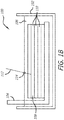
FIG. 1B is a schematic cross-sectional view of the system ofFIG. 1A . -
FIG. 1C is an enlarged cross-sectional view of the optical element manufactured by the system ofFIG. 1A . -
FIG. 2 is a photograph of a cross-section of an optical element manufactured by the system ofFIG. 1A demonstrating defects, as shown inFIG. 1C . -
FIG. 3 is a schematic isometric view showing a light beam traveling through an optical element manufactured by the system ofFIG. 1A . -
FIG. 4 is another schematic isometric view showing a light beam traveling through an optical element manufactured by the system ofFIG. 1A . -
FIG. 5 is a schematic cross-sectional view of a digital light processing projector stereolithography system for manufacturing of an optical element, not part of the present invention. -
FIG. 6 is a schematic isometric view showing a light beam traveling through an optical element manufactured by the system ofFIG. 5 . -
FIG. 7 is a schematic cross-sectional view of a system for additive manufacturing of a homogeneous optical element, according to the present invention. -
FIG. 8 is a schematic cross-sectional view of another system for additive manufacturing of a homogeneous optical element according to the present invention. -
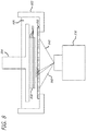
FIG. 9 is a schematic cross-sectional view of another system for additive manufacturing of a homogeneous optical element, not part of the present invention. -
FIG. 10 is a flow chart of a process for producing a homogeneous optical element, according to the present invention. -
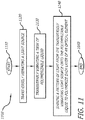
FIG. 11 is a flow chart of another process for producing a homogeneous optical element, not part of the present invention. - Throughout this description, elements appearing in figures are assigned three-digit reference designators, where the most significant digit is the figure number and the two least significant digits are specific to the element. An element that is not described in conjunction with a figure may be presumed to have the same characteristics and function as a previously-described element having a reference designator with the same least significant digits.
- An effective and innovative approach to improve the quality and optical performance of three-dimensional (3D) printed lenses is described herein. Systems and methods for increasing homogeneity of optical elements are described herein.
- Optical elements, such as lenses or spectacle lenses, can be made in any suitable shape and geometry by an additive manufacturing process. Stereo lithography (SLA) 3D printers are one such method. SLA printers can be adapted to different growing strategies, can be used on top of different growing platforms and/or substrates, and are fast.
- Manufacturing of spectacle lenses by additive processes provides some advantages for lens manufacturers, eye care practitioners and final customers (i.e., the lens user). Lens manufacturers may make lenses from scratch, without the need to buy and stock any blanks. Also, the additive manufacturing method is more environmentally friendly, as little or no waste is generated. Plus, making lenses by additive processes requires less energy than traditional techniques.
- SLA printers create objects as a set of 3D pixels, also called voxels. The 3D objects made from those voxels may not be homogenous. Physical and chemical properties of the material may change across the interfaces between voxels. In particular, local density and refractive index can be two of the physical properties that change across the interfaces between voxels. The optical effect of these changes in the lens material, once the lens is grown in the SLA printer, is that light scatters and diffracts as it goes through the 3D printed lens, decreasing its optical performance.
- SLA printing generally consists of shining ultra-violet (UV) light (e.g., with a wavelength of between 350nm and 420nm) in a very controlled way on a liquid resin contained in a tank. The UV light causes the resin to polymerize and turn into a solid. The desired object has a digital representation which is sliced into many layers. Each solid layer can be created on a previous solid layer by the polymerization of a liquid polymer layer through exposure to a pattern or image of UV light, e.g., from a scanning UV laser or a digital light processing (DLP) projector. With either the scanning laser or the DLP projector, the UV light shined on the resin is highly directional, and voxel structures are created on the polymer layer due to the pixels on the DLP projector image or lines made by the scanning laser.
- Referring now to
FIGs. 1A ,1B , and1C , a scanning laser SLA system includes aliquid resin 106 is inside atank 102, and asupport 104 to support anoptical element 108 is immersed in theresin 106. As used herein, the term optical element includes lenses and spectacle lenses. Alaser beam 112, e.g., a UV laser beam directed by ascanning mirror 118, impinges at different angles on theresin 106 along scanninglines 120 and polymerizes theresin 106 to formlayers 110 of theoptical element 108. - Light from the
laser beam 112 is directional, and anydefect 114, such as a dust spot or bubble, on the surface of or in the resin can create a tube-like shadow along the direction of the impinginglaser beam 112, causing a variation in irradiance and polymerization rate. The irradiance along this shadow may considerably differ from the irradiance at other points. The variation in polymerization rate can result in a non-homogeneousoptical element 108 withdefects 116, shown inFIG. 1C . The photographic microscope image ofFIG. 2 shows a non-homogeneous optical element manufactured by a scanning laser SLA system, such as shown inFIGs. 1A and1B . Thedefects 116 in the optical element resulting from thedefects 114 in theresin 106 can have a linear shape oriented along the direction of the incoming light, but can be randomly distributed across the layers. Referring again toFIG. 2 , horizontaldark lines 210 are the boundaries between layers, and vertical lines are variations of refractive index along the growing direction, caused by local variations of irradiance of the incoming light. In particular, micro-bubbles 214 created the tube-like structures 216. Similarly, other vertical lines were created by other defects not necessarily contained in the field of the photographic microscope image. As a result, the refractive index of theoptical element 108 can vary, causing scatter light and inhibiting optical quality. -
FIG. 3 shows alight beam 320 traveling through a non-homogeneousoptical element 308 manufactured by the system ofFIGs. 1A ,1B , and1C . When thelight beam 320 impinges on the non-homogeneousoptical element 308 withdefects 316, e.g., variations in refractive index, thelight beam 320 can be scattered, e.g., conically scattered 322, in an undesired manner as it passes through theoptical element 308. - Returning again to
FIG. 1A , the overlapping of scanninglines 120 can produce some variation of irradiance. Since perfect matching of irradiance along consecutive scans is difficult or impossible, scanning of thelaser beam 112 can produce a periodic irradiance pattern (e.g., a one-dimensional pattern) along the direction perpendicular to the line scans 120. Periodic irradiance can result in periodic variation of polymerization and a variation of physical properties of theoptical element 108, such as refractive index. As shown inFIG. 4 , when a light beam 420 impinges on a non-homogeneousoptical element 408 with a periodic variation inrefractive index 409, the light beam 420 will be diffracted into light beams 428a and 428b in an undesired manner. - Referring now to
FIG. 5 , a DLP projector SLA system includes atank 502 containing aresin 506 and a support 504 to support anoptical element 508 submerged in theresin 506. TheDLP projector 530 can direct a pattern oflight 540, e.g., UV light, on theresin 506 and polymerize theresin 506 to formlayers 510 of theoptical element 508. In the example shown inFIG. 5 , the pattern oflight 540 is directed through a transparent portion of the tank 502 (e.g., aglass bottom 532 of the tank). Polymer layers 510 of theoptical element 508 are created on the support 504 (e.g., growing platform), such that theoptical element 508 is created upside down. The DLP projectors can be based in any digital technology, such as liquid crystal display (LCD) filters and digital micromirror devices (DMDs). An advantage of DLP projector SLA systems is a faster printing process because an entire layer can be exposed at the same time. DLP projector SLA systems also have a simpler, more compact, and more cost-effective setup than a scanning laser SLA system. - Light from the DLP projector is strongly directional and local variations of irradiance between pixels or
defects 514 will cast a shadow on thelayer 510 that will produce a local variation of physical properties, such as refractive index. Defects on the glass, micro-bubbles on or in the resin, and irradiance variation from the pixels can produce a random set of defects in theoptical element 508, similar to thedefects 316 onoptical element 308, shown inFIG. 3 . These defects can propagate along the polymerization light direction and produce conical scattering. - Even if there were no defects and all pixels shined the same, significant variations of irradiance in the boundary between adjacent pixels would exist due to a fill factor of a light modulator used in the DLP projector being less than 100%, which can produce a two-dimensional periodic variation in the refractive index of the layer. As such, a pixel layout of a light modulator used in the
DLP projector 530 can produce a regular, periodic two-dimensional variation of refractive index within eachlayer 510. -
FIG. 6 shows alight beam 620 traveling through a non-homogeneous optical element 608 manufactured by the system ofFIG. 5 . When thelight beam 620 impinges on the non-homogeneous optical element 608 with a two-dimensional periodic variation inrefractive index 609, the emerginglight 634 will be diffracted, inhibiting the optical properties of the optical element 608. - To make an optical element with suitable optical properties with an SLA printer, scattering and diffraction effects must be reduced to negligible amounts. With respect to DLP projector SLA printers, the periodic structure of light irradiance caused by the pixels of the digital light projector must be minimized.
- A DLP projector SLA system that minimizes scattering and diffraction effects by changing light impinging on the resin from directional to non-directional or diffuse is shown in
FIG. 7 . Here, periodic transverse variations of irradiance on the resin are reduced or eliminated. Thetank 702 has atransparent portion 732, e.g., glass portion, between aDLP projector 730 and asupport 704 for anoptical element 708 so that light 740 from theDLP projector 730 passes through the transparent 732 to polymerizeresin 706 to form eachlayer 710 of theoptical element 708. Adiffuser 736, e.g., a thin layer described in more detail below of a diffuser, is positioned between thetransparent portion 736 and theresin 706 such that the light 740 passes through and is diffused by thediffuser 736 prior to impinging on theresin 706. - Because the
diffuser 736 is close to the forminglayer 710, the shape of the forminglayer 710 will be preserved. With adiffuser 736 of sufficient diffusing properties, the directional properties of the light 740 from the DLP projector will be interrupted.Light 740 will impinge from different directions at various points on theresin 706. For example, light from points A and B on thediffuser 736 overlaps on the forminglayer 710. As a result, shadows cast on the resin from defects are reduced or eliminated. The diffuser can also mix light from the pixel/inter-pixel structure to create a homogeneous irradiance pattern for thelayer 710. - SLA printers may use a non-sticking material on the transparent portion, e.g., a silicone compound or a PTFE (polytetrafluoroethylene) film. For a silicone-based film, a diffusive material, such as compatible dyes, micro particles, or nano-particle aggregates, can be incorporated into the film to create the
diffuser 736. For example, a 200 micron thick silicone-based film can be applied on thetransparent portion 732, where compatible dyes are incorporated in the film in quantities up to 3% of the weight of the film. The diffusive properties of this film are sufficient to reduce or eliminate both pixelation and directionality of the light from the DLP projector without significant light absorption. - In another example of an effective diffuser, a thin opal glass layer from 10 to 100 microns thick positioned on the
transparent portion 732 can form thediffuser 736. Opal glass has excellent diffusing characteristics, and can behave as a lambertian diffuser. - In yet another example of an effective diffuser, a holographic diffuser is positioned on the
glass 732 to precisely control the amount of scattering and fine tune the balance between available power and light diffusion. For example, a holographic diffuser can be formed from photopolymers. A holographic diffuser can be formed by embossing or machining a small scale pattern on a material with desired optical properties. - Another version of a DLP projector system that minimizes scattering and diffraction effects is shown in
FIG. 8 . A back surface of atransparent portion 850, for example, a glass portion, of tank 802 betweenoptical element 808 andDLP projector 830 windows can be made diffusive by grinding thetransparent portion 850 with a grinder of adequate grit, for example, aluminum oxide with 400 grit number. - Another version of a DLP projector SLA system that minimizes scattering and diffraction effects is shown in
FIG. 9 . Quasi-random transverse vibration ofDLP projector 930 and/or tank 902 can change light impinging on theresin 906 from directional to non-directional or diffuse and reduce or destroy periodical transverse variations of irradiance. A vibration device 960, e.g., an XY piezoelectric device, can be commanded to move in a transverse direction 962 (e.g., along an X axis and/or an Y axis) with a random amplitude the size of 1.5 pixels. The period of the vibration can be less than a tenth of the polymerization time per layer. For example, modern piezoelectric actuators or voice-coil actuators can create this movement. Vibration of only theDLP projector 930 may not remove the effect of linear defects on theresin 906 causing conical scattering. To remove these defects, avibration device 970, e.g., a piezoelectric device, should also vibrate the tank 902 in a transverse direction 972. In another version of the DLP projector SLA system, a mechanical vibrator to vibrate theglass 950 may be added to enhance removal of these defects. - Referring to
FIG. 10 , aprocess 1000 of creating homogeneous optical elements by additive manufacturing that starts at 1010 and ends at 1040 is shown. At 1020, a diffuser is positioned between a light source, e.g., a UV light source with a wavelength of between 350nm and 420nm, and a polymerizable liquid, such as a polymerizable resin. At 1030, a pattern of light from the light source is shined through the diffuser onto the polymerizable liquid to polymerize each layer of an optical element. This process may be implemented according to one of the DLP projector SLA systems described above inFIGs. 7 and8 . - Referring to
FIG. 11 , anotherprocess 1100 of creating homogeneous optical elements by additive manufacturing that starts at 1110 and ends at 1140 is shown. At 1120, a light source, e.g., a UV light source with a wavelength of between 350nm and 420nm, is transversely vibrated. At 1130, a tank of a polymerizable liquid, such as a polymerizable resin, is transversely vibrated. At 1140, a pattern of light from the transversely vibrated light source is shined onto the polymerizable liquid to polymerize each layer of an optical element. This process may be implemented according to the DLP projector SLA systems described above inFIG. 9 . - The systems and methods described herein are particularly suitable for prescription eyewear and ophthalmic lenses but may also be used for improving any lenses or optical elements made by an additive process.
- The lenses may be produced with the contour of the frame it will be put in, and optical and ergonomic criteria can be taken into account during lens design. The systems and methods described herein have as a prerequisite that the optimum surfaces -- arc, curvature, and the likeof the lens have been computed and properly described according to techniques known to those skilled in the art.
- The polymerizable liquid material is a monomer, oligomer, or prepolymer which can be cured to a solid transparent polymer in response to application of UV light (e.g., with a wavelength of between 350nm and 420nm) or other curing agent. The polymerizable liquid materials include monomers, oligomers, polyester resins, acrylic resins, and epoxy resins.
- Throughout this description, the embodiments and examples shown should be considered as exemplars, rather than limitations on the apparatus and procedures disclosed or claimed. Although many of the examples presented herein involve specific combinations of method acts or system elements, it should be understood that those acts and those elements may be combined in other ways to accomplish the same objectives. With regard to flowcharts, additional and fewer steps may be taken, and the steps as shown may be combined or further refined to achieve the methods described herein. Acts, elements and features discussed only in connection with one embodiment are not intended to be excluded from a similar role in other embodiments.
- As used herein, "plurality" means two or more. As used herein, a "set" of items may include one or more of such items. As used herein, whether in the written description or the claims, the terms "comprising", "including", "carrying", "having", "containing", "involving", and the like are to be understood to be open-ended, that is, to mean including but not limited to. Only the transitional phrases "consisting of' and "consisting essentially of', respectively, are closed or semi-closed transitional phrases with respect to claims. Use of ordinal terms such as "first", "second", "third", etc., in the claims to modify a claim element does not by itself connote any priority, precedence, or order of one claim element over another or the temporal order in which acts of a method are performed, but are used merely as labels to distinguish one claim element having a certain name from another element having a same name (but for use of the ordinal term) to distinguish the claim elements. As used herein, "and/or" means that the listed items are alternatives, but the alternatives also include any combination of the listed items.
Claims (21)
- A method for additive manufacturing an optical element (708,808) formed of layers (710,810) , the method comprising:positioning a diffuser (736, 850) between a light source and a light polymerizable liquid,wherein the diffuser (736, 850) is in contact with the light polymerizable liquid; wherein the light polymerizable liquid is a UV light polymerizable resin (706, 806); andfor each of the layers (710, 810) of the optical element (708,808), shining a pattern of light from thelight source through the diffuser (736, 850) onto the light polymerizable liquid tohomogeneously polymerize the layer (710, 810) wherein the light (740,840) impinging on the UV light polymerizable resin from the light source is changed from directional to non-directional wherein the resin (706,806) is in contact with a transparent portion (732, 850) of a tank (702,802) in which theresin (706, 806) is contained, said transparent portion (732, 850) is between the light source and a support (704, 804) for the optical element (708, 808) so that the light (740, 840) from the light source passes through the transparent portion (732, 850) to polymerize the resin (706, 806).
- The method of claim 1, wherein the diffuser (736, 850) comprises silicone.
- The method of claim 1, wherein the diffuser (736, 850) is a silicone film comprising a dye.
- The method of claim 3, wherein the silicone film is about 200 microns thick.
- The method of claim 3, wherein the dye is up to 3% of the weight of the silicone film.
- The method of claim 1, wherein the diffuser (736, 850) comprises an opal glass layer.
- The method of claim 6, wherein the opal glass layer is between 9 microns and 101 microns thick.
- The method of claim 1, wherein the diffuser (736, 850) is a holographic diffuser.
- The method of claim 1, wherein the diffuser is a ground surface of the tank (702,802) holding the light polymerizable liquid.
- The method of claim 1, wherein the diffuser (736, 850) is positioned on the transparent portion (732, 850) of the tank (702, 802) holding the light polymerizable liquid.
- The method of claim 1, wherein the light source is UV light with a wavelength of between 350nm and 420nm.
- The method of claim 1, wherein the light source is a digital light processing projector (730,830).
- A system for additively manufacturing an optical element (708,808) formed of layers (710, 810), the system comprising:a light source to generate a pattern of light for each layer (710,810) of the optical element (708,808);a diffuser (736, 850) positioned between the light source and a UV light polymerizable liquid, the system to homogenize the pattern of light for each layer and to change the light (740,840) from the light source from directional to non-directional wherein polymerizable liquid is a UV light polymerizable resin (706, 806) in contact with a transparent portion (732, 850) of a tank (702, 802) in which the resin (706, 806) is contained, said transparent portion (732, 850) is between the light source and a support (704, 804) for the optical element (708, 808) so that light (740, 840) from the light source passes through the transparent portion (732, 850) to polymerize the resin (706, 806),the light polymerizable liquid to polymerize each layer (710,810) in response to receiving the pattern of light for that layer (710,810), whereinthe diffuser (736, 850) is in contact with the light polymerizable liquid.
- The system of claim 13, wherein the light source is a digital light processing projector (730,830).
- The system of claim 13, wherein the diffuser (736, 850) comprises silicone.
- The system of claim 13, wherein the diffuser (736, 850) is a silicone film comprising a dye.
- The system of claim 16, wherein the silicone film is about 200 microns thick.
- The system of claim 16, wherein the dye is up to 3% of the weight of the silicone film.
- The system of claim 13, wherein the diffuser comprises an opal glass layer.
- The system of claim 19, wherein the opal glass layer is between about 10 microns and about 100 microns thick.
- The system of claim 13, wherein the diffuser (736, 850) is a holographic diffuser.
Applications Claiming Priority (2)
| Application Number | Priority Date | Filing Date | Title |
|---|---|---|---|
| US15/004,567 US10363710B2 (en) | 2016-01-22 | 2016-01-22 | Creating homogeneous optical elements by additive manufacturing |
| PCT/US2017/013674 WO2017127334A1 (en) | 2016-01-22 | 2017-01-16 | Creating homogeneous optical elements by additive manufacturing |
Publications (3)
| Publication Number | Publication Date |
|---|---|
| EP3405330A1 EP3405330A1 (en) | 2018-11-28 |
| EP3405330A4 EP3405330A4 (en) | 2019-09-11 |
| EP3405330B1 true EP3405330B1 (en) | 2021-08-18 |
Family
ID=59359446
Family Applications (1)
| Application Number | Title | Priority Date | Filing Date |
|---|---|---|---|
| EP17741799.5A Active EP3405330B1 (en) | 2016-01-22 | 2017-01-16 | Creating homogeneous optical elements by additive manufacturing |
Country Status (7)
| Country | Link |
|---|---|
| US (1) | US10363710B2 (en) |
| EP (1) | EP3405330B1 (en) |
| JP (1) | JP6784764B2 (en) |
| CN (1) | CN109311222A (en) |
| AU (1) | AU2017208985A1 (en) |
| CA (1) | CA3011252A1 (en) |
| WO (1) | WO2017127334A1 (en) |
Families Citing this family (18)
| Publication number | Priority date | Publication date | Assignee | Title |
|---|---|---|---|---|
| CN107457404B (en) * | 2017-08-02 | 2021-01-05 | 华中科技大学 | Additive machining forming method suitable for complex parts and dies |
| EP3473418B1 (en) * | 2017-10-19 | 2023-12-06 | Essilor International | Method for manufacturing an ophthalmic lens |
| WO2019183595A1 (en) | 2018-03-23 | 2019-09-26 | NanoPath, Inc. | Transparent illumination photolithography methods and systems |
| CN110920056A (en) * | 2018-09-04 | 2020-03-27 | 三纬国际立体列印科技股份有限公司 | Methods to improve the flatness of 3D printing surfaces |
| US10807311B2 (en) | 2018-09-10 | 2020-10-20 | Rebecca Metcalf | Additive manufacturing device with IR targeting and related methods |
| US12576588B2 (en) | 2019-02-21 | 2026-03-17 | Sprintray, Inc. | Reservoir with substrate assembly for reducing separation forces in three-dimensional printing |
| EP3698968A1 (en) | 2019-02-22 | 2020-08-26 | Essilor International | Method and system for manufacturing an optical volume element from a hardenable material using an additive manufacturing technology |
| EP3708368B1 (en) | 2019-03-14 | 2022-08-24 | DENTSPLY SIRONA Inc. | Method of operating a stereolithography apparatus for preventing adhesion of a 3d-object to the vat through oscillatory excitations |
| CN114072274B (en) * | 2019-06-24 | 2025-04-04 | 依视路国际公司 | Method and machine for producing optical components by additive manufacturing |
| EP3756863A1 (en) * | 2019-06-24 | 2020-12-30 | Essilor International | Method and system for outputting a manufacturing file for producing an optical element |
| CN110524874B (en) * | 2019-08-23 | 2022-03-08 | 源秩科技(上海)有限公司 | Photocuring 3D printing device and printing method thereof |
| US11633907B2 (en) * | 2020-10-16 | 2023-04-25 | Indizen Optical Technologies S.L. | Eyewear lens creation using additive techniques with diffuse light |
| US11919228B2 (en) * | 2020-12-23 | 2024-03-05 | Formlabs, Inc. | Techniques for improved additive fabrication on a film surface and related systems and methods |
| CR20230602A (en) * | 2021-06-09 | 2024-05-28 | Luxcreo Beijing Inc | Additive manufacturing apparatus and method |
| US12220866B2 (en) | 2021-06-09 | 2025-02-11 | Luxcreo Inc. | Additive manufacturing devices and methods |
| AU2023382064A1 (en) * | 2022-11-15 | 2025-05-29 | Zydex Pty Ltd | Apparatus and method for making a stereolithographic |
| EP4385708A1 (en) * | 2022-12-13 | 2024-06-19 | Essilor International | Method for additively manufacturing an ophthalmic device and manufacturing system configured to carry out such a method |
| US20260061701A1 (en) * | 2024-08-28 | 2026-03-05 | Indizen Optical Technologies S.L. | Eyewear lens creation by additive manufacturing using improved light pattern techniques |
Family Cites Families (21)
| Publication number | Priority date | Publication date | Assignee | Title |
|---|---|---|---|---|
| JPH04156326A (en) * | 1990-10-19 | 1992-05-28 | Fuji Photo Film Co Ltd | Shaping method using non-light emitting type display device |
| JPH04156325A (en) * | 1990-10-19 | 1992-05-28 | Fuji Photo Film Co Ltd | Shaping method using non-light emitting type display device and apparatus therefor |
| JPH0694979A (en) * | 1992-09-14 | 1994-04-08 | Nikon Corp | Camera with line-of-sight detection device |
| JPH07205303A (en) * | 1994-01-14 | 1995-08-08 | Mitsubishi Heavy Ind Ltd | Optical device for fine processing apparatus |
| JPH1184372A (en) * | 1997-09-05 | 1999-03-26 | Toppan Printing Co Ltd | Reflective liquid crystal display |
| US6505937B1 (en) | 2000-03-31 | 2003-01-14 | Titmus Optical, Inc. | Test slide for a vision testing apparatus |
| US20040159340A1 (en) | 2002-11-11 | 2004-08-19 | Hiatt William M. | Methods for removing and reclaiming unconsolidated material from substrates following fabrication of objects thereon by programmed material consolidation techniques |
| TW200626365A (en) * | 2004-09-27 | 2006-08-01 | Sumitomo Chemical Co | Light diffusing plate |
| DE102006060781B4 (en) * | 2006-09-29 | 2021-09-16 | Pictiva Displays International Limited | Organic light source |
| DE102009031915A1 (en) | 2009-07-06 | 2011-01-13 | Osram Opto Semiconductors Gmbh | A composition for producing a filter material for radiation, a method for producing a composition for a filter material, a material for filtering radiation and an optoelectronic component comprising the material |
| JP5609615B2 (en) | 2010-12-16 | 2014-10-22 | ウシオ電機株式会社 | Laser light source device |
| US10534114B2 (en) | 2010-12-31 | 2020-01-14 | Luminit LLC. | Substrate-guided holographic diffuser |
| US8721097B2 (en) * | 2011-05-19 | 2014-05-13 | Taiwan Semiconductor Manufacturing Company, Ltd. | LED lamp with improved light output |
| WO2013006970A1 (en) * | 2011-07-11 | 2013-01-17 | Raytheon Company | Compact light homogenizer |
| SG10201508107WA (en) * | 2012-03-30 | 2015-10-29 | Johnson & Johnson Vision Care | Methods and apparatus for forming a translating multifocal contact lens |
| TWI448732B (en) * | 2012-05-03 | 2014-08-11 | Young Optics Inc | Three-dimensional printing apparatus |
| WO2015072921A1 (en) * | 2013-11-14 | 2015-05-21 | Structo Pte. Ltd | Additive manufacturing device and method |
| US9952448B2 (en) * | 2014-03-26 | 2018-04-24 | Indizen Optical Technologies, S.L. | Eyewear lens production by additive techniques |
| US9933632B2 (en) | 2014-03-26 | 2018-04-03 | Indizen Optical Technologies, S.L. | Eyewear lens production by multi-layer additive techniques |
| WO2015197495A1 (en) * | 2014-06-27 | 2015-12-30 | Koninklijke Philips N.V. | Printing device and method for 3d printing |
| CN104802414A (en) * | 2015-05-20 | 2015-07-29 | 京东方科技集团股份有限公司 | Three-dimensional printing device and three-dimensional printing method |
-
2016
- 2016-01-22 US US15/004,567 patent/US10363710B2/en active Active
-
2017
- 2017-01-16 CN CN201780007205.4A patent/CN109311222A/en active Pending
- 2017-01-16 JP JP2018536295A patent/JP6784764B2/en active Active
- 2017-01-16 AU AU2017208985A patent/AU2017208985A1/en not_active Abandoned
- 2017-01-16 CA CA3011252A patent/CA3011252A1/en not_active Abandoned
- 2017-01-16 WO PCT/US2017/013674 patent/WO2017127334A1/en not_active Ceased
- 2017-01-16 EP EP17741799.5A patent/EP3405330B1/en active Active
Non-Patent Citations (1)
| Title |
|---|
| None * |
Also Published As
| Publication number | Publication date |
|---|---|
| EP3405330A1 (en) | 2018-11-28 |
| JP2019508283A (en) | 2019-03-28 |
| US20170210072A1 (en) | 2017-07-27 |
| WO2017127334A1 (en) | 2017-07-27 |
| US10363710B2 (en) | 2019-07-30 |
| CA3011252A1 (en) | 2017-07-27 |
| AU2017208985A1 (en) | 2018-08-02 |
| EP3405330A4 (en) | 2019-09-11 |
| CN109311222A (en) | 2019-02-05 |
| JP6784764B2 (en) | 2020-11-11 |
Similar Documents
| Publication | Publication Date | Title |
|---|---|---|
| US10363710B2 (en) | Creating homogeneous optical elements by additive manufacturing | |
| US12285909B2 (en) | High-throughput 3D printing of customized aspheric imaging lenses | |
| ES2826800T3 (en) | Spectacle lens and procedure for its manufacture | |
| KR101886615B1 (en) | Laser confocal sensor metrology system | |
| JP5267174B2 (en) | Stereolithography apparatus and modeling base | |
| ES2718918T3 (en) | Procedure and manufacturing system of an ophthalmic lens | |
| WO2019169960A1 (en) | Internal stereo direct light curing molding 3d printing device and control method therefor | |
| JP2017516155A (en) | Creation of eyewear and lenses using multilayer additive technology | |
| JP2021507279A (en) | Optical system | |
| EP3218166B1 (en) | Eyewear lens production by additive techniques | |
| US12269205B2 (en) | Eyewear lens creation using additive techniques with diffuse light | |
| US20260061701A1 (en) | Eyewear lens creation by additive manufacturing using improved light pattern techniques | |
| Christopher et al. | 3D printing optical components for microscopy using a desktop 3D printer | |
| US20260014754A1 (en) | Resin containment techniques for the additive manufacturing of eye wear lenses | |
| EP4349579A1 (en) | Method for manufacturing an optical device comprising a microstructure, manufacturing system to carry out such a method, and optical device thus obtained | |
| EP4385708A1 (en) | Method for additively manufacturing an ophthalmic device and manufacturing system configured to carry out such a method | |
| WO2024229533A1 (en) | 3d printing methods and light guides made therefrom | |
| JP2023061044A (en) | Light guide plate | |
| BR122022020382B1 (en) | GLASSES LENS |
Legal Events
| Date | Code | Title | Description |
|---|---|---|---|
| STAA | Information on the status of an ep patent application or granted ep patent |
Free format text: STATUS: THE INTERNATIONAL PUBLICATION HAS BEEN MADE |
|
| PUAI | Public reference made under article 153(3) epc to a published international application that has entered the european phase |
Free format text: ORIGINAL CODE: 0009012 |
|
| STAA | Information on the status of an ep patent application or granted ep patent |
Free format text: STATUS: REQUEST FOR EXAMINATION WAS MADE |
|
| 17P | Request for examination filed |
Effective date: 20180820 |
|
| AK | Designated contracting states |
Kind code of ref document: A1 Designated state(s): AL AT BE BG CH CY CZ DE DK EE ES FI FR GB GR HR HU IE IS IT LI LT LU LV MC MK MT NL NO PL PT RO RS SE SI SK SM TR |
|
| AX | Request for extension of the european patent |
Extension state: BA ME |
|
| DAV | Request for validation of the european patent (deleted) | ||
| DAX | Request for extension of the european patent (deleted) | ||
| A4 | Supplementary search report drawn up and despatched |
Effective date: 20190814 |
|
| RIC1 | Information provided on ipc code assigned before grant |
Ipc: G02C 7/02 20060101ALI20190808BHEP Ipc: G02B 3/00 20060101ALI20190808BHEP Ipc: B29C 67/00 20170101AFI20190808BHEP |
|
| STAA | Information on the status of an ep patent application or granted ep patent |
Free format text: STATUS: EXAMINATION IS IN PROGRESS |
|
| 17Q | First examination report despatched |
Effective date: 20200619 |
|
| GRAP | Despatch of communication of intention to grant a patent |
Free format text: ORIGINAL CODE: EPIDOSNIGR1 |
|
| STAA | Information on the status of an ep patent application or granted ep patent |
Free format text: STATUS: GRANT OF PATENT IS INTENDED |
|
| GRAJ | Information related to disapproval of communication of intention to grant by the applicant or resumption of examination proceedings by the epo deleted |
Free format text: ORIGINAL CODE: EPIDOSDIGR1 |
|
| STAA | Information on the status of an ep patent application or granted ep patent |
Free format text: STATUS: EXAMINATION IS IN PROGRESS |
|
| INTG | Intention to grant announced |
Effective date: 20210120 |
|
| GRAP | Despatch of communication of intention to grant a patent |
Free format text: ORIGINAL CODE: EPIDOSNIGR1 |
|
| INTC | Intention to grant announced (deleted) | ||
| STAA | Information on the status of an ep patent application or granted ep patent |
Free format text: STATUS: GRANT OF PATENT IS INTENDED |
|
| INTG | Intention to grant announced |
Effective date: 20210311 |
|
| GRAS | Grant fee paid |
Free format text: ORIGINAL CODE: EPIDOSNIGR3 |
|
| GRAA | (expected) grant |
Free format text: ORIGINAL CODE: 0009210 |
|
| STAA | Information on the status of an ep patent application or granted ep patent |
Free format text: STATUS: THE PATENT HAS BEEN GRANTED |
|
| AK | Designated contracting states |
Kind code of ref document: B1 Designated state(s): AL AT BE BG CH CY CZ DE DK EE ES FI FR GB GR HR HU IE IS IT LI LT LU LV MC MK MT NL NO PL PT RO RS SE SI SK SM TR |
|
| REG | Reference to a national code |
Ref country code: GB Ref legal event code: FG4D |
|
| REG | Reference to a national code |
Ref country code: CH Ref legal event code: EP |
|
| REG | Reference to a national code |
Ref country code: DE Ref legal event code: R096 Ref document number: 602017044285 Country of ref document: DE |
|
| REG | Reference to a national code |
Ref country code: IE Ref legal event code: FG4D Ref country code: AT Ref legal event code: REF Ref document number: 1421249 Country of ref document: AT Kind code of ref document: T Effective date: 20210915 |
|
| REG | Reference to a national code |
Ref country code: LT Ref legal event code: MG9D |
|
| REG | Reference to a national code |
Ref country code: NL Ref legal event code: MP Effective date: 20210818 |
|
| REG | Reference to a national code |
Ref country code: AT Ref legal event code: MK05 Ref document number: 1421249 Country of ref document: AT Kind code of ref document: T Effective date: 20210818 |
|
| PG25 | Lapsed in a contracting state [announced via postgrant information from national office to epo] |
Ref country code: RS Free format text: LAPSE BECAUSE OF FAILURE TO SUBMIT A TRANSLATION OF THE DESCRIPTION OR TO PAY THE FEE WITHIN THE PRESCRIBED TIME-LIMIT Effective date: 20210818 Ref country code: SE Free format text: LAPSE BECAUSE OF FAILURE TO SUBMIT A TRANSLATION OF THE DESCRIPTION OR TO PAY THE FEE WITHIN THE PRESCRIBED TIME-LIMIT Effective date: 20210818 Ref country code: HR Free format text: LAPSE BECAUSE OF FAILURE TO SUBMIT A TRANSLATION OF THE DESCRIPTION OR TO PAY THE FEE WITHIN THE PRESCRIBED TIME-LIMIT Effective date: 20210818 Ref country code: ES Free format text: LAPSE BECAUSE OF FAILURE TO SUBMIT A TRANSLATION OF THE DESCRIPTION OR TO PAY THE FEE WITHIN THE PRESCRIBED TIME-LIMIT Effective date: 20210818 Ref country code: FI Free format text: LAPSE BECAUSE OF FAILURE TO SUBMIT A TRANSLATION OF THE DESCRIPTION OR TO PAY THE FEE WITHIN THE PRESCRIBED TIME-LIMIT Effective date: 20210818 Ref country code: NO Free format text: LAPSE BECAUSE OF FAILURE TO SUBMIT A TRANSLATION OF THE DESCRIPTION OR TO PAY THE FEE WITHIN THE PRESCRIBED TIME-LIMIT Effective date: 20211118 Ref country code: PT Free format text: LAPSE BECAUSE OF FAILURE TO SUBMIT A TRANSLATION OF THE DESCRIPTION OR TO PAY THE FEE WITHIN THE PRESCRIBED TIME-LIMIT Effective date: 20211220 Ref country code: BG Free format text: LAPSE BECAUSE OF FAILURE TO SUBMIT A TRANSLATION OF THE DESCRIPTION OR TO PAY THE FEE WITHIN THE PRESCRIBED TIME-LIMIT Effective date: 20211118 Ref country code: AT Free format text: LAPSE BECAUSE OF FAILURE TO SUBMIT A TRANSLATION OF THE DESCRIPTION OR TO PAY THE FEE WITHIN THE PRESCRIBED TIME-LIMIT Effective date: 20210818 Ref country code: LT Free format text: LAPSE BECAUSE OF FAILURE TO SUBMIT A TRANSLATION OF THE DESCRIPTION OR TO PAY THE FEE WITHIN THE PRESCRIBED TIME-LIMIT Effective date: 20210818 |
|
| PG25 | Lapsed in a contracting state [announced via postgrant information from national office to epo] |
Ref country code: PL Free format text: LAPSE BECAUSE OF FAILURE TO SUBMIT A TRANSLATION OF THE DESCRIPTION OR TO PAY THE FEE WITHIN THE PRESCRIBED TIME-LIMIT Effective date: 20210818 Ref country code: LV Free format text: LAPSE BECAUSE OF FAILURE TO SUBMIT A TRANSLATION OF THE DESCRIPTION OR TO PAY THE FEE WITHIN THE PRESCRIBED TIME-LIMIT Effective date: 20210818 Ref country code: GR Free format text: LAPSE BECAUSE OF FAILURE TO SUBMIT A TRANSLATION OF THE DESCRIPTION OR TO PAY THE FEE WITHIN THE PRESCRIBED TIME-LIMIT Effective date: 20211119 |
|
| PG25 | Lapsed in a contracting state [announced via postgrant information from national office to epo] |
Ref country code: NL Free format text: LAPSE BECAUSE OF FAILURE TO SUBMIT A TRANSLATION OF THE DESCRIPTION OR TO PAY THE FEE WITHIN THE PRESCRIBED TIME-LIMIT Effective date: 20210818 |
|
| PG25 | Lapsed in a contracting state [announced via postgrant information from national office to epo] |
Ref country code: DK Free format text: LAPSE BECAUSE OF FAILURE TO SUBMIT A TRANSLATION OF THE DESCRIPTION OR TO PAY THE FEE WITHIN THE PRESCRIBED TIME-LIMIT Effective date: 20210818 |
|
| REG | Reference to a national code |
Ref country code: DE Ref legal event code: R097 Ref document number: 602017044285 Country of ref document: DE |
|
| PG25 | Lapsed in a contracting state [announced via postgrant information from national office to epo] |
Ref country code: SM Free format text: LAPSE BECAUSE OF FAILURE TO SUBMIT A TRANSLATION OF THE DESCRIPTION OR TO PAY THE FEE WITHIN THE PRESCRIBED TIME-LIMIT Effective date: 20210818 Ref country code: SK Free format text: LAPSE BECAUSE OF FAILURE TO SUBMIT A TRANSLATION OF THE DESCRIPTION OR TO PAY THE FEE WITHIN THE PRESCRIBED TIME-LIMIT Effective date: 20210818 Ref country code: RO Free format text: LAPSE BECAUSE OF FAILURE TO SUBMIT A TRANSLATION OF THE DESCRIPTION OR TO PAY THE FEE WITHIN THE PRESCRIBED TIME-LIMIT Effective date: 20210818 Ref country code: EE Free format text: LAPSE BECAUSE OF FAILURE TO SUBMIT A TRANSLATION OF THE DESCRIPTION OR TO PAY THE FEE WITHIN THE PRESCRIBED TIME-LIMIT Effective date: 20210818 Ref country code: CZ Free format text: LAPSE BECAUSE OF FAILURE TO SUBMIT A TRANSLATION OF THE DESCRIPTION OR TO PAY THE FEE WITHIN THE PRESCRIBED TIME-LIMIT Effective date: 20210818 Ref country code: AL Free format text: LAPSE BECAUSE OF FAILURE TO SUBMIT A TRANSLATION OF THE DESCRIPTION OR TO PAY THE FEE WITHIN THE PRESCRIBED TIME-LIMIT Effective date: 20210818 |
|
| PLBE | No opposition filed within time limit |
Free format text: ORIGINAL CODE: 0009261 |
|
| STAA | Information on the status of an ep patent application or granted ep patent |
Free format text: STATUS: NO OPPOSITION FILED WITHIN TIME LIMIT |
|
| 26N | No opposition filed |
Effective date: 20220519 |
|
| PG25 | Lapsed in a contracting state [announced via postgrant information from national office to epo] |
Ref country code: IT Free format text: LAPSE BECAUSE OF FAILURE TO SUBMIT A TRANSLATION OF THE DESCRIPTION OR TO PAY THE FEE WITHIN THE PRESCRIBED TIME-LIMIT Effective date: 20210818 |
|
| PG25 | Lapsed in a contracting state [announced via postgrant information from national office to epo] |
Ref country code: SI Free format text: LAPSE BECAUSE OF FAILURE TO SUBMIT A TRANSLATION OF THE DESCRIPTION OR TO PAY THE FEE WITHIN THE PRESCRIBED TIME-LIMIT Effective date: 20210818 Ref country code: MC Free format text: LAPSE BECAUSE OF FAILURE TO SUBMIT A TRANSLATION OF THE DESCRIPTION OR TO PAY THE FEE WITHIN THE PRESCRIBED TIME-LIMIT Effective date: 20210818 |
|
| REG | Reference to a national code |
Ref country code: CH Ref legal event code: PL |
|
| REG | Reference to a national code |
Ref country code: BE Ref legal event code: MM Effective date: 20220131 |
|
| PG25 | Lapsed in a contracting state [announced via postgrant information from national office to epo] |
Ref country code: LU Free format text: LAPSE BECAUSE OF NON-PAYMENT OF DUE FEES Effective date: 20220116 |
|
| PG25 | Lapsed in a contracting state [announced via postgrant information from national office to epo] |
Ref country code: BE Free format text: LAPSE BECAUSE OF NON-PAYMENT OF DUE FEES Effective date: 20220131 |
|
| PG25 | Lapsed in a contracting state [announced via postgrant information from national office to epo] |
Ref country code: LI Free format text: LAPSE BECAUSE OF NON-PAYMENT OF DUE FEES Effective date: 20220131 Ref country code: CH Free format text: LAPSE BECAUSE OF NON-PAYMENT OF DUE FEES Effective date: 20220131 |
|
| PG25 | Lapsed in a contracting state [announced via postgrant information from national office to epo] |
Ref country code: IE Free format text: LAPSE BECAUSE OF NON-PAYMENT OF DUE FEES Effective date: 20220116 |
|
| PG25 | Lapsed in a contracting state [announced via postgrant information from national office to epo] |
Ref country code: HU Free format text: LAPSE BECAUSE OF FAILURE TO SUBMIT A TRANSLATION OF THE DESCRIPTION OR TO PAY THE FEE WITHIN THE PRESCRIBED TIME-LIMIT; INVALID AB INITIO Effective date: 20170116 |
|
| PG25 | Lapsed in a contracting state [announced via postgrant information from national office to epo] |
Ref country code: MK Free format text: LAPSE BECAUSE OF FAILURE TO SUBMIT A TRANSLATION OF THE DESCRIPTION OR TO PAY THE FEE WITHIN THE PRESCRIBED TIME-LIMIT Effective date: 20210818 Ref country code: CY Free format text: LAPSE BECAUSE OF FAILURE TO SUBMIT A TRANSLATION OF THE DESCRIPTION OR TO PAY THE FEE WITHIN THE PRESCRIBED TIME-LIMIT Effective date: 20210818 |
|
| PG25 | Lapsed in a contracting state [announced via postgrant information from national office to epo] |
Ref country code: MT Free format text: LAPSE BECAUSE OF FAILURE TO SUBMIT A TRANSLATION OF THE DESCRIPTION OR TO PAY THE FEE WITHIN THE PRESCRIBED TIME-LIMIT Effective date: 20210818 |
|
| PG25 | Lapsed in a contracting state [announced via postgrant information from national office to epo] |
Ref country code: TR Free format text: LAPSE BECAUSE OF FAILURE TO SUBMIT A TRANSLATION OF THE DESCRIPTION OR TO PAY THE FEE WITHIN THE PRESCRIBED TIME-LIMIT Effective date: 20210818 |
|
| PGFP | Annual fee paid to national office [announced via postgrant information from national office to epo] |
Ref country code: GB Payment date: 20260127 Year of fee payment: 10 |
|
| PGFP | Annual fee paid to national office [announced via postgrant information from national office to epo] |
Ref country code: DE Payment date: 20260128 Year of fee payment: 10 |
|
| PGFP | Annual fee paid to national office [announced via postgrant information from national office to epo] |
Ref country code: FR Payment date: 20260126 Year of fee payment: 10 |