EP3404832A1 - Rf phase shifting device - Google Patents
Rf phase shifting device Download PDFInfo
- Publication number
- EP3404832A1 EP3404832A1 EP17171725.9A EP17171725A EP3404832A1 EP 3404832 A1 EP3404832 A1 EP 3404832A1 EP 17171725 A EP17171725 A EP 17171725A EP 3404832 A1 EP3404832 A1 EP 3404832A1
- Authority
- EP
- European Patent Office
- Prior art keywords
- amplifier
- signal
- output
- input
- phase shifting
- Prior art date
- Legal status (The legal status is an assumption and is not a legal conclusion. Google has not performed a legal analysis and makes no representation as to the accuracy of the status listed.)
- Granted
Links
Images



Classifications
-
- H—ELECTRICITY
- H03—ELECTRONIC CIRCUITRY
- H03H—IMPEDANCE NETWORKS, e.g. RESONANT CIRCUITS; RESONATORS
- H03H11/00—Networks using active elements
- H03H11/02—Multiple-port networks
- H03H11/16—Networks for phase shifting
-
- H—ELECTRICITY
- H03—ELECTRONIC CIRCUITRY
- H03F—AMPLIFIERS
- H03F3/00—Amplifiers with only discharge tubes or only semiconductor devices as amplifying elements
- H03F3/20—Power amplifiers, e.g. Class B amplifiers, Class C amplifiers
- H03F3/21—Power amplifiers, e.g. Class B amplifiers, Class C amplifiers with semiconductor devices only
- H03F3/211—Power amplifiers, e.g. Class B amplifiers, Class C amplifiers with semiconductor devices only using a combination of several amplifiers
-
- H—ELECTRICITY
- H03—ELECTRONIC CIRCUITRY
- H03F—AMPLIFIERS
- H03F1/00—Details of amplifiers with only discharge tubes, only semiconductor devices or only unspecified devices as amplifying elements
- H03F1/02—Modifications of amplifiers to raise the efficiency, e.g. gliding Class A stages, use of an auxiliary oscillation
- H03F1/0205—Modifications of amplifiers to raise the efficiency, e.g. gliding Class A stages, use of an auxiliary oscillation in transistor amplifiers
- H03F1/0211—Modifications of amplifiers to raise the efficiency, e.g. gliding Class A stages, use of an auxiliary oscillation in transistor amplifiers with control of the supply voltage or current
- H03F1/0216—Continuous control
-
- H—ELECTRICITY
- H03—ELECTRONIC CIRCUITRY
- H03F—AMPLIFIERS
- H03F3/00—Amplifiers with only discharge tubes or only semiconductor devices as amplifying elements
- H03F3/189—High-frequency amplifiers, e.g. radio frequency amplifiers
- H03F3/19—High-frequency amplifiers, e.g. radio frequency amplifiers with semiconductor devices only
-
- H—ELECTRICITY
- H03—ELECTRONIC CIRCUITRY
- H03F—AMPLIFIERS
- H03F3/00—Amplifiers with only discharge tubes or only semiconductor devices as amplifying elements
- H03F3/45—Differential amplifiers
- H03F3/45071—Differential amplifiers with semiconductor devices only
-
- H—ELECTRICITY
- H03—ELECTRONIC CIRCUITRY
- H03F—AMPLIFIERS
- H03F3/00—Amplifiers with only discharge tubes or only semiconductor devices as amplifying elements
- H03F3/60—Amplifiers in which coupling networks have distributed constants, e.g. with waveguide resonators
- H03F3/602—Combinations of several amplifiers
-
- H—ELECTRICITY
- H03—ELECTRONIC CIRCUITRY
- H03F—AMPLIFIERS
- H03F3/00—Amplifiers with only discharge tubes or only semiconductor devices as amplifying elements
- H03F3/68—Combinations of amplifiers, e.g. multi-channel amplifiers for stereophonics
-
- H—ELECTRICITY
- H03—ELECTRONIC CIRCUITRY
- H03H—IMPEDANCE NETWORKS, e.g. RESONANT CIRCUITS; RESONATORS
- H03H11/00—Networks using active elements
- H03H11/02—Multiple-port networks
- H03H11/16—Networks for phase shifting
- H03H11/20—Two-port phase shifters providing an adjustable phase shift
-
- H—ELECTRICITY
- H03—ELECTRONIC CIRCUITRY
- H03F—AMPLIFIERS
- H03F2200/00—Indexing scheme relating to amplifiers
- H03F2200/204—A hybrid coupler being used at the output of an amplifier circuit
-
- H—ELECTRICITY
- H03—ELECTRONIC CIRCUITRY
- H03F—AMPLIFIERS
- H03F2200/00—Indexing scheme relating to amplifiers
- H03F2200/336—A I/Q, i.e. phase quadrature, modulator or demodulator being used in an amplifying circuit
-
- H—ELECTRICITY
- H03—ELECTRONIC CIRCUITRY
- H03F—AMPLIFIERS
- H03F2200/00—Indexing scheme relating to amplifiers
- H03F2200/423—Amplifier output adaptation especially for transmission line coupling purposes, e.g. impedance adaptation
-
- H—ELECTRICITY
- H03—ELECTRONIC CIRCUITRY
- H03F—AMPLIFIERS
- H03F2200/00—Indexing scheme relating to amplifiers
- H03F2200/451—Indexing scheme relating to amplifiers the amplifier being a radio frequency amplifier
-
- H—ELECTRICITY
- H03—ELECTRONIC CIRCUITRY
- H03F—AMPLIFIERS
- H03F2200/00—Indexing scheme relating to amplifiers
- H03F2200/541—Transformer coupled at the output of an amplifier
-
- H—ELECTRICITY
- H03—ELECTRONIC CIRCUITRY
- H03F—AMPLIFIERS
- H03F2200/00—Indexing scheme relating to amplifiers
- H03F2200/72—Indexing scheme relating to amplifiers the amplifier stage being a common gate configuration MOSFET
-
- H—ELECTRICITY
- H03—ELECTRONIC CIRCUITRY
- H03F—AMPLIFIERS
- H03F2200/00—Indexing scheme relating to amplifiers
- H03F2200/75—Indexing scheme relating to amplifiers the amplifier stage being a common source configuration MOSFET
-
- H—ELECTRICITY
- H03—ELECTRONIC CIRCUITRY
- H03F—AMPLIFIERS
- H03F2203/00—Indexing scheme relating to amplifiers with only discharge tubes or only semiconductor devices as amplifying elements covered by H03F3/00
- H03F2203/45—Indexing scheme relating to differential amplifiers
- H03F2203/45228—A transformer being added at the output or the load circuit of the dif amp
Definitions
- the present inventive concept relates to a phase shifting device comprising an input amplifier, output amplifiers and a differential quadrature hybrid coupler.
- phase shifting devices may be used for providing an output signal having a controllable phase.
- the phase shifting device may comprise a power splitter for splitting an input signal into preferably two different output ports, and various means for combining the split signal into an output signal having the desired phase.
- Phase shifting devices are e.g. utilized in phased array systems, in which an array of antennas creates a beam of radio waves which can be electronically steered to point in different directions without moving the antennas.
- the steering of the beam may be enabled by the phase shifting devices, which may be arranged at each antenna path for controlling the signal phase of the radio frequency current from the transmitter.
- phased array systems constitute one example of applications wherein the phase shifting devices may be used.
- phase shifting devices capable of providing smaller phase steps, reduced amplitude variation over the phase steps, and a reduced power consumption.
- An objective of the present inventive concept is accordingly to provide a phase shifting device which is more compact and allows for a reduced power consumption. Additional and alternative objectives may be understood from the following.
- a phase shifting device comprising an input amplifier, a biasing circuit, a first output amplifier, a second output amplifier, and a quadrature hybrid coupler.
- the input amplifier may be connected to an input port of the coupler, the first output amplifier to a through port of the coupler, the second output amplifier to a coupled port of the coupler, and the biasing circuit to an isolated port of the coupler.
- the hybrid coupler may be configured to receive, at the input port, an input signal from the input amplifier, to output, at the through port, a through signal, to receive, at the isolated port, a bias signal from the biasing circuit, and to output, at the coupled port, a coupled signal having a phase differing from a phase of the through signal.
- the first output amplifier and the second output amplifier may be variable-gain amplifiers.
- the input amplifier may be used to drive the input port of the coupler and to provide current to the first output amplifier, i.e., the variable-gain amplifier at the through port of the coupler.
- the quadrature hybrid coupler which e.g. may be of a lumped or distributed configuration, may comprise a terminated fourth terminal, i.e., an isolated port
- a biasing circuit may be arranged to bias the isolated port and thereby provide current to the second output amplifier at the coupled port.
- the biasing circuit may be a duplicated version of the input amplifier, but it does not necessarily act as an amplifier providing an input signal. Instead, the biasing circuit may be arranged to merely provide a biasing current to the second output amplifier, matching the current in the in-phase branch of the coupler.
- variable-gain amplifiers at the through port and coupled port, a multilevel modulation of the resulting in-phase/coupled signal, output from the coupler, may be achieved.
- the phase shifting device may be configured to operate on a differential signal, i.e., a signal formed of a differential signal pair.
- the hybrid coupler may be a differential hybrid coupler, connected to differential amplifiers.
- the input amplifier may be a common source amplifier.
- a common source amplifier may be understood as a device comprising a transistor in which the signal enters the gate and exits the drain terminal.
- the input amplifier may hence act as a transconductance amplifier, in which the input voltage may modulate the current flowing through the amplifier and being fed to the input port of the coupler.
- the common source amplifier is advantageous in that is may provide more gain as compared to a common gate amplifier, and may be combined with common gate output amplifiers in a cascode configuration.
- the cascode configuration allows for the amplifiers to share current source and to provide a reduced power consumption.
- the input amplifier may be a differential amplifier that amplifies the difference between two input voltages and outputs a voltage that, ideally, may be proportional to the difference between the two input voltages.
- the differential amplifier may comprise a differential pair of common source amplifiers, in which the differential pair of transistors may have a current source connected to their respective sources for setting a biasing current and provide common mode suppression.
- the input amplifier may be a pseudo-differential amplifier, in which the current source may be removed and the biasing controlled by the gates of the common source transistors. This configuration may leave more headroom for the signal swing, since there one transistor less is required between the supply and the ground.
- the structure forming the input amplifier may be the same as the structure forming the biasing circuit.
- the input amplifier structure may be duplicated so as to provide a biasing current to match the current in the in-phase branch of the coupler.
- the first and, preferably, also the second output amplifier may comprise common gate amplifiers.
- the common gate amplifier should be understood as a device comprising a transistor in which the source terminal of the transistor serves as the input, the drain is the output and the gate may be connected to a fixed potential serving as a virtual ground for the AC signals.
- the signal from the differential through port and/or coupled port of the coupler may enter the source and exit through the drain terminal.
- the common gate amplifier is advantageous in that is has a relatively low input impedance, which may facilitate matching with the characteristic impedance of the coupler in a relatively compact manner.
- the first and second output amplifier may be differential amplifiers similar to what is described with reference to the input amplifier.
- the input and/or input amplifiers may e.g. comprise field-effect transistors (FETs).
- FETs field-effect transistors
- the phase shifting device may comprise a common source input amplifier and two common gate output amplifiers, with the differential quadrature hybrid coupler arranged to receive the input signal from the common source input amplifier and to output the through signal and the coupled signal to the first and second common gate output amplifier, respectively.
- the input amplifier and the output amplifiers may thus form a cascode amplifier, with the coupler arranged between the common source amplifier and the common gate amplifier.
- the common source amplifier may conduct in response to a gate voltage being applied to its gate, whereas the common gate output amplifiers may conduct due to the potential difference now appearing between their gate and source terminals.
- the cascode arrangement is advantageous in that the source voltage of the common gate output amplifier may be held at a substantially constant voltage during operation, which allows for the common gate output amplifier to exhibit a relatively low input resistance to the common source input amplifier. This allows for the input resistance of the input amplifier to be matched with the required impedance of the hybrid coupler. Further, cascode configuration allows for the common gate output amplifiers to share the current with the common source input amplifier.
- the transistor of the common gate output amplifier may have an increased gate length compared to the transistor of the common source input amplifier, so as to increase the output conductance of the output amplifier.
- the gate length By increasing the gate length, the impact of the loading impedance on the source impedance of the output amplifier may be reduced.
- each of the first and second output amplifiers may comprise a plurality of unit transistors that are interconnected to control the through signal and the coupled signal, respectively.
- the unit transistors may be individually controlled by bit lines, which, in case of common gate transistors, may act on the gate terminal of the transistor for turning on and off the transistor.
- This type of controllable transistor structures may also be referred to as variable-gain amplifiers, such as e.g. digital variable-gain amplifiers, which allows for the amplitude of the in-phase signal and the coupled signal to be varied.
- the first and second output amplifiers may be formed of a set of binary weighted transistors that can be used for combining the in-phase signal and the coupled signal into a desired output signal.
- each of the variable-gain amplifiers comprises four binary weighted transistors that allow for a 4-bit control of the output current.
- an additional, second set of binary weighted transistors may be added. These transistors may be formed of a similar structure as the above-described first transistor structure, which advantageously may be duplicated.
- This second set of transistors may act as dummy transistors that connect to the V DD and which may be used to keep the total number of switched-on unit transistors of the amplifier constant.
- a unit transistor of a certain size is switched off, a corresponding dummy transistor of the additional set may be switched on to keep the current substantially constant. This allows for a compensation of the impedance variations during the switching of the transistors, resulting in the coupler seeing a relatively stable, fixed impedance.
- the use of such a second set of binary switched transistors hence allows for the input impedance to be maintained at a relatively fixed level for the different switching states, thereby improving the operation of the coupler.
- the dummy transistors may be controlled by inverted bit lines, such that a dummy transistor of the additional set may be turned on when the corresponding unit transistor is switched off.
- the first set of binary weighted transistor (and also the set of dummy transistors) only allows a limited range of combinations of the in-phase signal and coupled signal.
- the coupled signal is a quadrature signal, having a phase shift of 90°
- combinations may be provided only in the first quadrant of the full 360° phase range. Therefore, a third set of transistors may be provided, which may be a duplicated version of the first transistor structure, and which may be connected to the opposite signal of the differential signal pair.
- a 180° phase shift may be achieved which allows for the full 360° phase range to be reached. In this way, an additional control bit may be provided, which allows of the resulting combined output signal to be formed also of a negative in-phase and/or coupled signal.
- the third set of transistors allows for a 5-bit control of the output current.
- the phase shifting device may comprise a combining means connected to the first and second output amplifier.
- the combining means may be configured to combine the through signal (i.e., the in-phase signal) and the coupled signal into a combined output signal.
- the combining means may e.g. comprise a transformer, an inductor or a transmission line.
- the differential quadrature hybrid coupler may be a quadrature coupler comprising four coils arranged in a first layer and a second layer.
- the first layer and the second layer may be separated from each other by an intermediate dielectric layer.
- the first coil may be arranged such that at least one turn extends in the first layer and another turn extends in the second layer.
- the second coil may be arranged such that at least one turn extends in the first layer and another turn extends in the second layer.
- the at least one turn of the second coil arranged in the first layer is further arranged along at least a portion of the first coil arranged in the first layer, wherein the another turn of the second coil arranged in the second layer may be arranged along at least a portion of the first coil arranged in the second layer.
- the third coil may be arranged such that at least one turn of the third coil extends in the first layer and superposes at least a portion of the first coil arranged in the second layer, and such that another turn of the third coil extends in the second layer and is superposed by at least a portion of the first coil arranged in the first layer.
- the fourth coil may extend in the first layer and superposes at least a portion of the second coil arranged in the second layer, and such that another turn of the fourth coil extends in the second layer and is superposed by at least a portion of the second coil arranged in the first layer.
- the differential input port may be formed by a first terminal of the first coil and a first terminal of the second coil, the differential through port by a second terminal of the first coil and a second terminal of the second coil, the differential coupled port by a second terminal of the third coil and a second terminal of the fourth coil, and the differential isolated port by a first terminal of the third coil and a first terminal of the fourth coil.
- Fig. 1 a illustrates a phase shifting device 100 according to an embodiment of the present inventive concept.
- the phase shifting device 100 may comprise an input amplifier 110, a differential quadrature hybrid coupler 150, two output amplifiers 130, 140 and a combining means 160.
- the phase shifting device 100 may be configured to receive, at the input amplifier 110, an input signal IN, which e.g. may comprise a differential pair of signals P, N.
- the input signal IN may be amplified by the input amplifier 110 to a level necessary for driving the input of the coupler 150.
- the coupler 150 the signal may be divided into two signals, a first one I which may be in phase with the input signal IN and a second, coupled signal Q which may have different phase ⁇ relative the in-phase signal I.
- the coupler is a quadrature hybrid coupler
- the coupled signal (or quadrature signal) Q may differ 90° from the in-phase signal I.
- the in-phase signal I and the coupled signal Q may be transmitted to the first output amplifier 130 and the second output amplifier 140, respectively, in which the different phases I, Q are weighted and transmitted to a combining means 160 to generate the desired output signal OUT.
- the output amplifiers 130, 140 may e.g. be digitally controlled variable amplifiers allowing a discrete number of combinations of the amplitude of the I and Q signals.
- Figure 1b is a schematic illustration of the phase components of the combined output signal OUT.
- the resulting output signal OUT is indicated by the arrow, and the phase difference by ⁇ .
- the amplitude of the in-phase signal I and the coupled signal Q may be scaled with the aim to keep the amplitude of the resulting output signal OUT approximately constant.
- four-bit output amplifiers may result in 256 different combinations in the first quadrant of the I/Q diagram. About 30 of the combinations, which are closest to the unity circle, may be preferred.
- Other quadrants may be used by swapping the polarity of the in-phase signal I and the coupled signal Q, resulting in a fifth control bit.
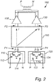
- Fig. 2 illustrates a phase shifting device 100 according to an embodiment, which may be similarly configured as the one described with reference to figure 1 a above.
- the phase shifting device 100 may comprise a coupling element, such as e.g. a quadrature hybrid coupler 150, for splitting an input signal IN into an in-phase signal I and a coupled signal Q.
- the coupler 150 may comprise an input port P1 and a through port P2, between which the input signal IN may be transmitted without having its phase shifted. Further, the coupler 150 may comprise a coupled port P3, at which the coupled (quadrature) signal Q may be provided.
- the coupler 150 may comprise a forth terminal, which may be an isolated or terminated port P4.
- the hybrid coupler may be a differential coupler for handling a differential signal P, N of the input signal IN.
- the input port P1 may be connected to an input amplifier 110, which e.g. may be a differential common source input amplifier 110 providing the necessary gain for driving the coupler 150.
- the input amplifier 110 may e.g. comprise a first common source amplifier 112, configured to receive the N signal of the differential pair of forming the input signal IN, and a second common source amplifier 114 that is configured to receive the P signal of the differential pair.
- the common source amplifiers 112, 114 may be formed of a respective field-effect transistor (FET) to which the input signal may be applied to the gate terminal and whose source terminal may be connected to ground.
- FET field-effect transistor
- a similar structure may be connected to the isolated port P4 of the coupler 150, thus forming a biasing circuit 120 comprising a first common source amplifier 122 and a second common source amplifier 124.
- the gate terminals of the respective transistors 122, 124 of the biasing circuit 120 may be connected to a common, biasing source Vg for supplying a matching current to the coupler 150.
- the through port P2 may be connected to a first output amplifier 130, which e.g. may be a differential variable-gain amplifier 130 configured to vary the amplitude of the in-phase signal I.
- a similar structure 140 may be arranged at the coupled port P3 for allowing the amplitude of the coupled signal Q to be varied.
- the performance of the coupler 150 may depend on parameters such as e.g. bandwidth, phase balance and amplitude balance of the coupler 150. These parameters may also be influenced by the loading of the outputs P2, P3 of the coupler 150. For proper operation of the coupler 150, the outputs P2, P3 of the coupler 150 may be terminated by an impedance corresponding to the characteristic impedance of the coupler 150. This impedance may e.g. be in the range of 30 to 100 Ohm.
- the phase shifting device 100 may further comprise a combining means, comprising e.g. a transformer 160, for combining the in-phase component I and the coupled component Q of the signal into a common output signal OUT, as described in connection with figure 1 b.
- a combining means comprising e.g. a transformer 160, for combining the in-phase component I and the coupled component Q of the signal into a common output signal OUT, as described in connection with figure 1 b.
- FIG 3 shows a schematic layout of a first output amplifier 130, which may be similarly configured as the amplifiers discussed in connection with figures 1 a and 2. Even though only the first output amplifier 130 will be described in detail in the following, it is appreciated that the same description, features and advantages may apply to the second output amplifier 140 as well.
- the output amplifier 130 may in some examples be a digitally controlled variable-gain amplifier (VGA), and may together with the second output amplifier 140 be configured to weigh the I/Q signals, generated by the coupler 150, separately and to generate the required phase at the combined output signal OUT.
- VGA digitally controlled variable-gain amplifier
- the VGA 130 may comprise a plurality of unit transistors T1, T2, T3, T4, whose operation may be individually controlled by dedicated bit lines (not shown).
- the unit transistors T1-T4 may be common gate transistors interconnected in a weighted amplifier structure, forming a first set of transistors 131, 132.
- Such transistors T1-T4 may provide an input impedance that is inversely proportional to their transconductance, thereby making relatively low impedances possible without any additional matching.
- the VGAs 130, 140 may comprise four binary weighted transistors T1-T4, arranged in a first amplifier structure 131 allowing a 4-bit control of the output current. It is preferable if the binary switched VGAs 130, 140 keep their input impedance relatively fixed for every switching state. However, changing the output current also changes the current at the source and thus the impedance seen at the source of the amplifier structure 131.
- an additional, second set 135, 136 of binary weighted transistors may be placed in parallel with the first amplifier structure 131.
- the second set 135, 136 of transistors may thus act as dummy transistors that connect to the V DD and are used to keep the total number of switched-on unit transistors constant.
- a unit transistor T1-T4 of a certain size is switched off in the first set 131, 132
- a corresponding dummy transistor of the second set 135, 136 may be switched on to keep the current in the output amplifier 130 substantially constant.
- the dummy transistors may be controlled by inverted bit lines, thereby allowing a dummy transistor of the second set 135, 136 to be turned on when the corresponding unit transistor T1-T4 is switched off.
- a third set of transistors 133 may be provided.
- the third set 133 may form a similar structure as the first amplifier structure 131, i.e., comprising a set of binary weighted unit transistors T1-T4, in which the positive signal N and the negative signal P of the differential signal pair of the in-phase signal I and the coupled signal Q are switched.
- the output of the first set 131, 132 and the third set 133, 134 may result in opposite polarities, which allows for the combined output signal OUT to be formed of both positive and negative I/Q combinations, i.e., combinations positioned also in the second, third and fourth quadrant of the I/Q diagram discussed in connection with figure 1 b.
- Figure 4 show a perspective view of a quadrature hybrid coupler 150 according to an embodiment, which may be similarly configured as the couplers 150 discussed in connection with the previous figures.
- the coupler 150 may comprise four coils 1100, 1200, 1300, 1400, each of which having at least four turns extending in a first layer and a second layer, respectively.
- the first coil 1100 may comprise a first terminal 1112 and a second terminal 1122 and may be arranged such that at least one turn 1110, forming a part of the coil 1100, extends in the first layer and at least another turn 1120 extends in the underlying, second layer.
- the first and second layers, and hence the respective turns 110, 1120 of the first coil 1100 may be separated from each other by an intermediate dielectric layer (not shown).
- the first terminal 1112 and the second terminal 1122 of the first coil 1100 may be arranged on a same side of the coupler 150 such that, during operation, power that is input at e.g. the first terminal 1112 may be output at the same side of the coupler 150.
- the second coil 1200 may be similarly arranged as the first coil 1100, extending in the first layer and the second layer and having a first terminal 1212 and a second terminal 1222. Further, the second coil 1200 may be arranged such that at least one turn 1210 of the second coil 1200 extends in the first layer and along at least a portion of the first coil 1100, i.e., along, or side by side with, at least a portion of the at least one turn 1110 arranged in the first layer. Further, another turn 1220 of the second coil may be arranged to extend in the second layer and along at least a portion of the first coil 1100, i.e., along at least a portion of the turn 1120 of the first coil 1100 arranged in the second layer.
- the first coil 1100 and the second coil 1200 can be described as two oppositely routed coils. Accordingly, the second terminal 1122 of the first coil 1100 is connected to the turn 1120 of the first coil 1100 that extends in the second layer, whereas the second terminal 1222 of the second coil 1200 is connected to the turn 1220 of the second coil 1200 that extends in the first layer.
- the second coil 1200 By arranging the second coil 1200 such that is at least partly extends along the first coil 1100 in a same plane, between the first coil 1100 and the second coil 1200, may be used to provide or modify the characteristic impedance of the coupler 150. Further, as a signal is provided at the first terminal 1112 and the second terminal 1212, the opposite routing of the first coil 1100 and the second coil 1200 allows for a differential signaling wherein the electromagnetic fields that are generated by the complementary signals P, N are directed in the same directions, thereby avoiding or at least reducing the risk of the magnetic fields canceling or counteracting each other.
- the third coil 1300 and the fourth coil 1400 maybe similarly arranged as the first coil 1100 and the second coil 1200. As indicated in the present figure, at least one turn 1310 of the third coil 1300 may be arranged to extend in the first layer and such that it superposes at least a portion 1120 of the first coil arranged in the second layer. Further, another turn 1320 of the third coil may be arranged to extend in the second layer and to superpose at least a portion 1110 of the first coil 1100 arranged in the first layer.
- an electromagnetic interaction may be provided.
- the electromagnetic interaction may allow for a transformer action between the first coil 1100 and the third coil 1300.
- the third coil 1300 may have a first terminal 1312 connected to the turn 1320 of the third coil 1300 that may be arranged in the second layer, and a second terminal 1322 connected to the turn 1310 of the third coil 1300 that may be arranged in the first layer.
- the fourth coil 1400 may comprise at least one turn 1410 that may be arranged to extend in the first layer and such that it superposes at least a portion 1220 of the second coil 1200 arranged in the second layer, and at least one turn 1420 that is arranged to extend in the second layer and such that it is superposed by at least a portion 1210 of the second coil 1200 arranged in the first layer. Further, the fourth coil 1400 may comprise a first terminal 1412 that may be connected to the turn 1410 arranged in the first layer, and a second terminal 1422 that is connected to the turn 1420 arranged in the second layer. Similarly to what is described above in connection to the third coil 1300, a transformer coupling may be provided between the fourth coil 1400 and the second coil 1200.
- the third coil 1300 and the fourth coil 1400 may be routed or operated in opposite directions, they may be used for differential signaling in a similar way as described with reference to the first coil 1100 and the second coil 1200.
- the coupler 150 may further comprise a differential input port P1 formed by the first terminal 1112 of the first coil 1100 and the first terminal 1212 of the second coil 1200.
- the second terminal 1122 of the first coil 1100 and the second terminal 1222 of the second coil 1200 may form a differential through port P2, wherein the differential input port P1 and the differential through port P2 may be arranged on the same side or opposite sides of the coupler 150.
- the first terminal 1312 of the third coil 1300 and the first terminal 1412 of the fourth coil 1400 may form a differential isolated port P4
- the second terminal 1322 of the third coil 1300 and a second terminal 1422 of the fourth coil 1400 may form a differential coupled port P3.
Landscapes
- Engineering & Computer Science (AREA)
- Power Engineering (AREA)
- Amplifiers (AREA)
Abstract
Description
- The present inventive concept relates to a phase shifting device comprising an input amplifier, output amplifiers and a differential quadrature hybrid coupler.
- In the prior art, phase shifting devices may be used for providing an output signal having a controllable phase. The phase shifting device may comprise a power splitter for splitting an input signal into preferably two different output ports, and various means for combining the split signal into an output signal having the desired phase.
- Phase shifting devices are e.g. utilized in phased array systems, in which an array of antennas creates a beam of radio waves which can be electronically steered to point in different directions without moving the antennas. The steering of the beam may be enabled by the phase shifting devices, which may be arranged at each antenna path for controlling the signal phase of the radio frequency current from the transmitter.
- The phased array systems constitute one example of applications wherein the phase shifting devices may be used. In order to improve the overall performance and efficiency of such systems and other applications wherein phase shifting devices may be used, there is a strive for phase shifting devices capable of providing smaller phase steps, reduced amplitude variation over the phase steps, and a reduced power consumption.
- An objective of the present inventive concept is accordingly to provide a phase shifting device which is more compact and allows for a reduced power consumption. Additional and alternative objectives may be understood from the following.
- According to an aspect of the present inventive concept there is provided a phase shifting device, comprising an input amplifier, a biasing circuit, a first output amplifier, a second output amplifier, and a quadrature hybrid coupler. The input amplifier may be connected to an input port of the coupler, the first output amplifier to a through port of the coupler, the second output amplifier to a coupled port of the coupler, and the biasing circuit to an isolated port of the coupler. Further, the hybrid coupler may be configured to receive, at the input port, an input signal from the input amplifier, to output, at the through port, a through signal, to receive, at the isolated port, a bias signal from the biasing circuit, and to output, at the coupled port, a coupled signal having a phase differing from a phase of the through signal. The first output amplifier and the second output amplifier may be variable-gain amplifiers.
- Thus, the input amplifier may be used to drive the input port of the coupler and to provide current to the first output amplifier, i.e., the variable-gain amplifier at the through port of the coupler. Since the quadrature hybrid coupler, which e.g. may be of a lumped or distributed configuration, may comprise a terminated fourth terminal, i.e., an isolated port, a biasing circuit may be arranged to bias the isolated port and thereby provide current to the second output amplifier at the coupled port. The biasing circuit may be a duplicated version of the input amplifier, but it does not necessarily act as an amplifier providing an input signal. Instead, the biasing circuit may be arranged to merely provide a biasing current to the second output amplifier, matching the current in the in-phase branch of the coupler.
- By using variable-gain amplifiers at the through port and coupled port, a multilevel modulation of the resulting in-phase/coupled signal, output from the coupler, may be achieved.
- The phase shifting device may be configured to operate on a differential signal, i.e., a signal formed of a differential signal pair. In such case, the hybrid coupler may be a differential hybrid coupler, connected to differential amplifiers.
- According to one embodiment, the input amplifier may be a common source amplifier. A common source amplifier may be understood as a device comprising a transistor in which the signal enters the gate and exits the drain terminal. The input amplifier may hence act as a transconductance amplifier, in which the input voltage may modulate the current flowing through the amplifier and being fed to the input port of the coupler. The common source amplifier is advantageous in that is may provide more gain as compared to a common gate amplifier, and may be combined with common gate output amplifiers in a cascode configuration. The cascode configuration allows for the amplifiers to share current source and to provide a reduced power consumption.
- According to an embodiment, the input amplifier may be a differential amplifier that amplifies the difference between two input voltages and outputs a voltage that, ideally, may be proportional to the difference between the two input voltages. The differential amplifier may comprise a differential pair of common source amplifiers, in which the differential pair of transistors may have a current source connected to their respective sources for setting a biasing current and provide common mode suppression. Alternatively, the input amplifier may be a pseudo-differential amplifier, in which the current source may be removed and the biasing controlled by the gates of the common source transistors. This configuration may leave more headroom for the signal swing, since there one transistor less is required between the supply and the ground.
- According to an embodiment, the structure forming the input amplifier may be the same as the structure forming the biasing circuit. In other words, the input amplifier structure may be duplicated so as to provide a biasing current to match the current in the in-phase branch of the coupler.
- According to an embodiment of the present inventive concept, the first and, preferably, also the second output amplifier may comprise common gate amplifiers. The common gate amplifier should be understood as a device comprising a transistor in which the source terminal of the transistor serves as the input, the drain is the output and the gate may be connected to a fixed potential serving as a virtual ground for the AC signals. Thus, the signal from the differential through port and/or coupled port of the coupler may enter the source and exit through the drain terminal. The common gate amplifier is advantageous in that is has a relatively low input impedance, which may facilitate matching with the characteristic impedance of the coupler in a relatively compact manner.
- The first and second output amplifier may be differential amplifiers similar to what is described with reference to the input amplifier.
- The input and/or input amplifiers may e.g. comprise field-effect transistors (FETs).
- In one embodiment, the phase shifting device may comprise a common source input amplifier and two common gate output amplifiers, with the differential quadrature hybrid coupler arranged to receive the input signal from the common source input amplifier and to output the through signal and the coupled signal to the first and second common gate output amplifier, respectively. The input amplifier and the output amplifiers may thus form a cascode amplifier, with the coupler arranged between the common source amplifier and the common gate amplifier. In such an arrangement, the common source amplifier may conduct in response to a gate voltage being applied to its gate, whereas the common gate output amplifiers may conduct due to the potential difference now appearing between their gate and source terminals. The cascode arrangement is advantageous in that the source voltage of the common gate output amplifier may be held at a substantially constant voltage during operation, which allows for the common gate output amplifier to exhibit a relatively low input resistance to the common source input amplifier. This allows for the input resistance of the input amplifier to be matched with the required impedance of the hybrid coupler. Further, cascode configuration allows for the common gate output amplifiers to share the current with the common source input amplifier.
- According to an embodiment, the transistor of the common gate output amplifier may have an increased gate length compared to the transistor of the common source input amplifier, so as to increase the output conductance of the output amplifier. By increasing the gate length, the impact of the loading impedance on the source impedance of the output amplifier may be reduced.
- According to an embodiment, each of the first and second output amplifiers may comprise a plurality of unit transistors that are interconnected to control the through signal and the coupled signal, respectively. The unit transistors may be individually controlled by bit lines, which, in case of common gate transistors, may act on the gate terminal of the transistor for turning on and off the transistor. This type of controllable transistor structures may also be referred to as variable-gain amplifiers, such as e.g. digital variable-gain amplifiers, which allows for the amplitude of the in-phase signal and the coupled signal to be varied.
- According to an embodiment, the first and second output amplifiers may be formed of a set of binary weighted transistors that can be used for combining the in-phase signal and the coupled signal into a desired output signal.
- In one example, each of the variable-gain amplifiers comprises four binary weighted transistors that allow for a 4-bit control of the output current.
- According to an embodiment, an additional, second set of binary weighted transistors may be added. These transistors may be formed of a similar structure as the above-described first transistor structure, which advantageously may be duplicated. This second set of transistors may act as dummy transistors that connect to the VDD and which may be used to keep the total number of switched-on unit transistors of the amplifier constant. Thus, when a unit transistor of a certain size is switched off, a corresponding dummy transistor of the additional set may be switched on to keep the current substantially constant. This allows for a compensation of the impedance variations during the switching of the transistors, resulting in the coupler seeing a relatively stable, fixed impedance. The use of such a second set of binary switched transistors hence allows for the input impedance to be maintained at a relatively fixed level for the different switching states, thereby improving the operation of the coupler. The dummy transistors may be controlled by inverted bit lines, such that a dummy transistor of the additional set may be turned on when the corresponding unit transistor is switched off.
- However, the first set of binary weighted transistor (and also the set of dummy transistors) only allows a limited range of combinations of the in-phase signal and coupled signal. In case the coupled signal is a quadrature signal, having a phase shift of 90°, combinations may be provided only in the first quadrant of the full 360° phase range. Therefore, a third set of transistors may be provided, which may be a duplicated version of the first transistor structure, and which may be connected to the opposite signal of the differential signal pair. By swapping the positive and negative signals of the differential signal pair, a 180° phase shift may be achieved which allows for the full 360° phase range to be reached. In this way, an additional control bit may be provided, which allows of the resulting combined output signal to be formed also of a negative in-phase and/or coupled signal.
- When combined with the 4-bit control provided by the binary weighted four transistor structure described above, the third set of transistors allows for a 5-bit control of the output current.
- According to an embodiment, the phase shifting device may comprise a combining means connected to the first and second output amplifier. The combining means may be configured to combine the through signal (i.e., the in-phase signal) and the coupled signal into a combined output signal. The combining means may e.g. comprise a transformer, an inductor or a transmission line.
- According to an embodiment, the differential quadrature hybrid coupler may be a quadrature coupler comprising four coils arranged in a first layer and a second layer. The first layer and the second layer may be separated from each other by an intermediate dielectric layer. The first coil may be arranged such that at least one turn extends in the first layer and another turn extends in the second layer. Similarly, the second coil may be arranged such that at least one turn extends in the first layer and another turn extends in the second layer. The at least one turn of the second coil arranged in the first layer is further arranged along at least a portion of the first coil arranged in the first layer, wherein the another turn of the second coil arranged in the second layer may be arranged along at least a portion of the first coil arranged in the second layer. The third coil may be arranged such that at least one turn of the third coil extends in the first layer and superposes at least a portion of the first coil arranged in the second layer, and such that another turn of the third coil extends in the second layer and is superposed by at least a portion of the first coil arranged in the first layer. The fourth coil may extend in the first layer and superposes at least a portion of the second coil arranged in the second layer, and such that another turn of the fourth coil extends in the second layer and is superposed by at least a portion of the second coil arranged in the first layer.
- The differential input port may be formed by a first terminal of the first coil and a first terminal of the second coil, the differential through port by a second terminal of the first coil and a second terminal of the second coil, the differential coupled port by a second terminal of the third coil and a second terminal of the fourth coil, and the differential isolated port by a first terminal of the third coil and a first terminal of the fourth coil.
- It is to be understood that the terminology used herein is for purpose of describing particular embodiments only, and is not intended to be limiting. It must be noted that, as used in the specification and the appended claim, the articles "a," "an," "the," and "said" are intended to mean that there are one or more of the elements unless the context clearly dictates otherwise. Thus, for example, reference to "a unit" or "the unit" may include several devices, and the like. Furthermore, the words "comprising", "including", "containing" and similar wordings does not exclude other elements or steps.
- The above, as well as additional objects, features and advantages of the present inventive concept, will be better understood through the following illustrative and non-limiting detailed description, with reference to the appended drawings. In the drawings like reference numerals will be used for like elements unless stated otherwise.
-
Figure 1 a illustrates a general schematic of a phase shifting device. -
Figure 1b is a diagram showing different amplitude combinations of the through signal and the coupled signal. -
Figure 2 shows a schematic of a phase shifting device according to an embodiment. -
Figure 3 shows a schematic of a variable-gain amplifier according to an embodiment. -
Figure 4 illustrates a perspective view of a coupler according to an embodiment. -
Fig. 1 a illustrates aphase shifting device 100 according to an embodiment of the present inventive concept. Thephase shifting device 100 may comprise aninput amplifier 110, a differentialquadrature hybrid coupler 150, twooutput amplifiers phase shifting device 100 may be configured to receive, at theinput amplifier 110, an input signal IN, which e.g. may comprise a differential pair of signals P, N. The input signal IN may be amplified by theinput amplifier 110 to a level necessary for driving the input of thecoupler 150. In thecoupler 150, the signal may be divided into two signals, a first one I which may be in phase with the input signal IN and a second, coupled signal Q which may have different phase ϕ relative the in-phase signal I. In case the coupler is a quadrature hybrid coupler, the coupled signal (or quadrature signal) Q may differ 90° from the in-phase signal I. - Subsequently, the in-phase signal I and the coupled signal Q may be transmitted to the
first output amplifier 130 and thesecond output amplifier 140, respectively, in which the different phases I, Q are weighted and transmitted to a combining means 160 to generate the desired output signal OUT. Theoutput amplifiers -
Figure 1b is a schematic illustration of the phase components of the combined output signal OUT. The resulting output signal OUT is indicated by the arrow, and the phase difference by ϕ. The amplitude of the in-phase signal I and the coupled signal Q may be scaled with the aim to keep the amplitude of the resulting output signal OUT approximately constant. Using e.g. four-bit output amplifiers may result in 256 different combinations in the first quadrant of the I/Q diagram. About 30 of the combinations, which are closest to the unity circle, may be preferred. Other quadrants may be used by swapping the polarity of the in-phase signal I and the coupled signal Q, resulting in a fifth control bit. -
Fig. 2 illustrates aphase shifting device 100 according to an embodiment, which may be similarly configured as the one described with reference tofigure 1 a above. Thephase shifting device 100 may comprise a coupling element, such as e.g. aquadrature hybrid coupler 150, for splitting an input signal IN into an in-phase signal I and a coupled signal Q. Thecoupler 150 may comprise an input port P1 and a through port P2, between which the input signal IN may be transmitted without having its phase shifted. Further, thecoupler 150 may comprise a coupled port P3, at which the coupled (quadrature) signal Q may be provided. Typically, thecoupler 150 may comprise a forth terminal, which may be an isolated or terminated port P4. It will be appreciated that the hybrid coupler may be a differential coupler for handling a differential signal P, N of the input signal IN. - The input port P1 may be connected to an
input amplifier 110, which e.g. may be a differential commonsource input amplifier 110 providing the necessary gain for driving thecoupler 150. Theinput amplifier 110 may e.g. comprise a firstcommon source amplifier 112, configured to receive the N signal of the differential pair of forming the input signal IN, and a secondcommon source amplifier 114 that is configured to receive the P signal of the differential pair. As indicated in the present figure, thecommon source amplifiers transistors - A similar structure may be connected to the isolated port P4 of the
coupler 150, thus forming abiasing circuit 120 comprising a firstcommon source amplifier 122 and a secondcommon source amplifier 124. As no input signal is needed on this port, the gate terminals of therespective transistors circuit 120 may be connected to a common, biasing source Vg for supplying a matching current to thecoupler 150. - The through port P2 may be connected to a
first output amplifier 130, which e.g. may be a differential variable-gain amplifier 130 configured to vary the amplitude of the in-phase signal I. Asimilar structure 140 may be arranged at the coupled port P3 for allowing the amplitude of the coupled signal Q to be varied. Theseoutput amplifiers figure 3 . - The performance of the
coupler 150 may depend on parameters such as e.g. bandwidth, phase balance and amplitude balance of thecoupler 150. These parameters may also be influenced by the loading of the outputs P2, P3 of thecoupler 150. For proper operation of thecoupler 150, the outputs P2, P3 of thecoupler 150 may be terminated by an impedance corresponding to the characteristic impedance of thecoupler 150. This impedance may e.g. be in the range of 30 to 100 Ohm. - The
phase shifting device 100 may further comprise a combining means, comprising e.g. atransformer 160, for combining the in-phase component I and the coupled component Q of the signal into a common output signal OUT, as described in connection withfigure 1 b. -
Figure 3 shows a schematic layout of afirst output amplifier 130, which may be similarly configured as the amplifiers discussed in connection withfigures 1 a and 2. Even though only thefirst output amplifier 130 will be described in detail in the following, it is appreciated that the same description, features and advantages may apply to thesecond output amplifier 140 as well. - The
output amplifier 130 may in some examples be a digitally controlled variable-gain amplifier (VGA), and may together with thesecond output amplifier 140 be configured to weigh the I/Q signals, generated by thecoupler 150, separately and to generate the required phase at the combined output signal OUT. - The
VGA 130 may comprise a plurality of unit transistors T1, T2, T3, T4, whose operation may be individually controlled by dedicated bit lines (not shown). In one example, the unit transistors T1-T4 may be common gate transistors interconnected in a weighted amplifier structure, forming a first set oftransistors - In the present example illustrated in
figure 3 , theVGAs first amplifier structure 131 allowing a 4-bit control of the output current. It is preferable if the binary switched VGAs 130, 140 keep their input impedance relatively fixed for every switching state. However, changing the output current also changes the current at the source and thus the impedance seen at the source of theamplifier structure 131. - Hence, an additional,
second set first amplifier structure 131. Thesecond set first set second set output amplifier 130 substantially constant. This allows for a compensation of the impedance variations during the switching of theVGAs coupler 150 seeing a relatively stable, fixed impedance and thus in an improved operation of thecoupler 150. The dummy transistors may be controlled by inverted bit lines, thereby allowing a dummy transistor of thesecond set - To reach the full 360° spectrum of combinations of the in-phase signal I and the coupled signal Q, a third set of
transistors 133 may be provided. Thethird set 133 may form a similar structure as thefirst amplifier structure 131, i.e., comprising a set of binary weighted unit transistors T1-T4, in which the positive signal N and the negative signal P of the differential signal pair of the in-phase signal I and the coupled signal Q are switched. In other words, the output of thefirst set third set figure 1 b. -
Figure 4 show a perspective view of aquadrature hybrid coupler 150 according to an embodiment, which may be similarly configured as thecouplers 150 discussed in connection with the previous figures. Thecoupler 150 may comprise fourcoils first coil 1100 may comprise afirst terminal 1112 and a second terminal 1122 and may be arranged such that at least one turn 1110, forming a part of thecoil 1100, extends in the first layer and at least another turn 1120 extends in the underlying, second layer. The first and second layers, and hence the respective turns 110, 1120 of thefirst coil 1100, may be separated from each other by an intermediate dielectric layer (not shown). - According to the present, exemplary embodiment, the
first terminal 1112 and the second terminal 1122 of thefirst coil 1100 may be arranged on a same side of thecoupler 150 such that, during operation, power that is input at e.g. the first terminal 1112 may be output at the same side of thecoupler 150. - The
second coil 1200 may be similarly arranged as thefirst coil 1100, extending in the first layer and the second layer and having afirst terminal 1212 and asecond terminal 1222. Further, thesecond coil 1200 may be arranged such that at least one turn 1210 of thesecond coil 1200 extends in the first layer and along at least a portion of thefirst coil 1100, i.e., along, or side by side with, at least a portion of the at least one turn 1110 arranged in the first layer. Further, another turn 1220 of the second coil may be arranged to extend in the second layer and along at least a portion of thefirst coil 1100, i.e., along at least a portion of the turn 1120 of thefirst coil 1100 arranged in the second layer. - By arranging the
first coil 1100 and thesecond coil 1200 such that thefirst terminal 112 of thefirst coil 1100 is connected to the turn 1110 of thefirst coil 1100 that extends in the first layer, and such that thefirst terminal 1212 of thesecond coil 1200 is connected to the turn 1220 of thesecond coil 1200 that extends in the second layer, thefirst coil 1100 and thesecond coil 1200 can be described as two oppositely routed coils. Accordingly, the second terminal 1122 of thefirst coil 1100 is connected to the turn 1120 of thefirst coil 1100 that extends in the second layer, whereas thesecond terminal 1222 of thesecond coil 1200 is connected to the turn 1220 of thesecond coil 1200 that extends in the first layer. By arranging thesecond coil 1200 such that is at least partly extends along thefirst coil 1100 in a same plane, between thefirst coil 1100 and thesecond coil 1200, may be used to provide or modify the characteristic impedance of thecoupler 150. Further, as a signal is provided at thefirst terminal 1112 and thesecond terminal 1212, the opposite routing of thefirst coil 1100 and thesecond coil 1200 allows for a differential signaling wherein the electromagnetic fields that are generated by the complementary signals P, N are directed in the same directions, thereby avoiding or at least reducing the risk of the magnetic fields canceling or counteracting each other. - The
third coil 1300 and thefourth coil 1400 maybe similarly arranged as thefirst coil 1100 and thesecond coil 1200. As indicated in the present figure, at least one turn 1310 of thethird coil 1300 may be arranged to extend in the first layer and such that it superposes at least a portion 1120 of the first coil arranged in the second layer. Further, another turn 1320 of the third coil may be arranged to extend in the second layer and to superpose at least a portion 1110 of thefirst coil 1100 arranged in the first layer. By arranging thethird coil 1300 such that it at least partly superposes thefirst coil 1100, i.e., such that thefirst coil 1100 and thethird coil 1300 are arranged in a stacked arrangement in relation to each other, an electromagnetic interaction may be provided. The electromagnetic interaction may allow for a transformer action between thefirst coil 1100 and thethird coil 1300. Thethird coil 1300 may have a first terminal 1312 connected to the turn 1320 of thethird coil 1300 that may be arranged in the second layer, and a second terminal 1322 connected to the turn 1310 of thethird coil 1300 that may be arranged in the first layer. - The
fourth coil 1400 may comprise at least one turn 1410 that may be arranged to extend in the first layer and such that it superposes at least a portion 1220 of thesecond coil 1200 arranged in the second layer, and at least one turn 1420 that is arranged to extend in the second layer and such that it is superposed by at least a portion 1210 of thesecond coil 1200 arranged in the first layer. Further, thefourth coil 1400 may comprise a first terminal 1412 that may be connected to the turn 1410 arranged in the first layer, and a second terminal 1422 that is connected to the turn 1420 arranged in the second layer. Similarly to what is described above in connection to thethird coil 1300, a transformer coupling may be provided between thefourth coil 1400 and thesecond coil 1200. - As the
third coil 1300 and thefourth coil 1400 may be routed or operated in opposite directions, they may be used for differential signaling in a similar way as described with reference to thefirst coil 1100 and thesecond coil 1200. - The
coupler 150 may further comprise a differential input port P1 formed by thefirst terminal 1112 of thefirst coil 1100 and thefirst terminal 1212 of thesecond coil 1200. The second terminal 1122 of thefirst coil 1100 and thesecond terminal 1222 of thesecond coil 1200 may form a differential through port P2, wherein the differential input port P1 and the differential through port P2 may be arranged on the same side or opposite sides of thecoupler 150. Similarly, thefirst terminal 1312 of thethird coil 1300 and thefirst terminal 1412 of thefourth coil 1400 may form a differential isolated port P4, whereas thesecond terminal 1322 of thethird coil 1300 and asecond terminal 1422 of thefourth coil 1400 may form a differential coupled port P3. - In the above the inventive concept has mainly been described with reference to a limited number of examples. However, as is readily appreciated by a person skilled in the art, other examples than the ones disclosed above are equally possible within the scope of the inventive concept, as defined by the appended claims.
Claims (14)
- A phase shifting device (100), comprising:an input amplifier (110);a biasing circuit (120);a first output amplifier (130);a second output amplifier (140); anda quadrature hybrid coupler (150);wherein:the input amplifier is connected to an input port (P1) of the coupler;the first output amplifier is connected to a through port (P2) of the coupler;the second output amplifier is connected to a coupled port (P3) of the coupler;the biasing circuit is connected to an isolated port (P4) of the coupler;wherein quadrature hybrid coupler is configured to:receive, at the input port, an input signal (IN) from the input amplifier;output, at the through port, a through signal (I);receive, at the isolated port, a bias signal from the biasing circuit; andoutput, at the coupled port, a coupled signal (Q) having a phase differing from a phase of the through signal;wherein the first output amplifier and the second output amplifier are variable-gain amplifiers.
- The phase shifting device according to claim 1, configured to operate on a differential input signal.
- The phase shifting device according to claim 2, wherein the input amplifier is a differential amplifier.
- The phase shifting device according to any one of the preceding claims, wherein the input amplifier is a common source amplifier.
- The phase shifting device according to claim 4, wherein the input amplifier is a pseudo-differential amplifier.
- The phase shifting device according to any one of the preceding claims, wherein the first and second output amplifiers are common gate amplifiers.
- The phase shifting device according to any one of the preceding claims, wherein the first and second output amplifiers are differential amplifiers.
- The phase shifting device according to any one of the preceding claims, wherein each of the first and second output amplifiers comprises a first set (131, 132) of a plurality of unit transistors (T1, T2, T3, T4) that are interconnected to control the through signal and the coupled signal, respectively.
- The phase shifting device according to claim 8, wherein the plurality of unit transistors form a binary weighted amplifier structure.
- The phase shifting device according to claim 8 or 9, wherein each of the first and second output amplifiers further comprises a second set (135, 136) of dummy transistors for compensating current variations in the first and second output amplifiers.
- The phase shifting device according to claim 10, wherein the unit transistors of the first set are individually operated by bit lines and wherein the dummy transistors of the second set are operated by inverted bit lines.
- The phase shifting device according to any one of claims 8 to 11, wherein each of the first and second output amplifiers further comprises a third set (133, 134) of transistors, wherein the first set and the third set of transistors are connected to opposite signals of a differential signal pair of the through signal and the coupled signal, respectively.
- The phase shifting device according to any one of the preceding claims, further comprising a combining means (160) connected to the first and second output amplifiers and configured to combine the through signal and the coupled signal into a combined output signal.
- The phase shifting device according to claim 13, wherein the combining means is a transformer, an inductor or a transmission line.
Priority Applications (2)
| Application Number | Priority Date | Filing Date | Title |
|---|---|---|---|
| EP17171725.9A EP3404832B1 (en) | 2017-05-18 | 2017-05-18 | Rf phase shifting device |
| US15/981,165 US10778190B2 (en) | 2017-05-18 | 2018-05-16 | RF phase shifting device |
Applications Claiming Priority (1)
| Application Number | Priority Date | Filing Date | Title |
|---|---|---|---|
| EP17171725.9A EP3404832B1 (en) | 2017-05-18 | 2017-05-18 | Rf phase shifting device |
Publications (2)
| Publication Number | Publication Date |
|---|---|
| EP3404832A1 true EP3404832A1 (en) | 2018-11-21 |
| EP3404832B1 EP3404832B1 (en) | 2020-02-12 |
Family
ID=58715116
Family Applications (1)
| Application Number | Title | Priority Date | Filing Date |
|---|---|---|---|
| EP17171725.9A Active EP3404832B1 (en) | 2017-05-18 | 2017-05-18 | Rf phase shifting device |
Country Status (2)
| Country | Link |
|---|---|
| US (1) | US10778190B2 (en) |
| EP (1) | EP3404832B1 (en) |
Cited By (2)
| Publication number | Priority date | Publication date | Assignee | Title |
|---|---|---|---|---|
| CN110601659A (en) * | 2019-08-28 | 2019-12-20 | 北京无线电测量研究所 | Active vector modulator |
| US11545950B2 (en) | 2019-06-03 | 2023-01-03 | Analog Devices, Inc. | Apparatus and methods for vector modulator phase shifters |
Families Citing this family (7)
| Publication number | Priority date | Publication date | Assignee | Title |
|---|---|---|---|---|
| US11569555B2 (en) * | 2019-12-06 | 2023-01-31 | Qualcomm Incorporated | Phase shifter with active signal phase generation |
| US11183973B1 (en) * | 2020-06-02 | 2021-11-23 | Samsung Electronics Co., Ltd | Method and circuit for power consumption reduction in active phase shifters |
| CN116671014A (en) * | 2020-12-23 | 2023-08-29 | 上海诺基亚贝尔股份有限公司 | Devices for processing radio frequency signals |
| CN114070299B (en) * | 2021-12-08 | 2025-06-13 | 苏州矽典微智能科技有限公司 | Fully differential coupler and broadband quadrature generator |
| US20240072402A1 (en) * | 2022-08-30 | 2024-02-29 | Texas Instruments Incorporated | Gain invariant bidirectional phase shifter |
| US20240429906A1 (en) * | 2023-06-23 | 2024-12-26 | Qualcomm Incorporated | Shared phase shifter radio architecture |
| US20250279564A1 (en) * | 2024-03-01 | 2025-09-04 | Apple Inc. | Compact phase shifter layout |
Citations (2)
| Publication number | Priority date | Publication date | Assignee | Title |
|---|---|---|---|---|
| US4511813A (en) * | 1981-06-12 | 1985-04-16 | Harris Corporation | Dual-gate MESFET combiner/divider for use in adaptive system applications |
| EP3109935A1 (en) * | 2015-06-26 | 2016-12-28 | IMEC vzw | Coupling element for differential hybrid coupler |
Family Cites Families (15)
| Publication number | Priority date | Publication date | Assignee | Title |
|---|---|---|---|---|
| US6496061B1 (en) * | 2000-10-10 | 2002-12-17 | Conexant Systems, Inc. | High efficiency multiple power level amplifier |
| WO2002045206A1 (en) * | 2000-11-28 | 2002-06-06 | Telefonaktiebolaget Lm Ericsson (Publ) | A radio frequency amplifying circuit |
| US6515541B2 (en) * | 2001-06-13 | 2003-02-04 | Skyworks Solutions, Inc. | Multi-level power amplifier |
| US6806768B2 (en) * | 2001-10-31 | 2004-10-19 | Qualcomm Incorporated | Balanced power amplifier with a bypass structure |
| US6743652B2 (en) * | 2002-02-01 | 2004-06-01 | Stmicroelectronics, Inc. | Method for making an integrated circuit device including photodiodes |
| EP1460437A1 (en) * | 2003-03-18 | 2004-09-22 | Agilent Technologies Inc | Power measurement apparatus and method therefor |
| US7215194B2 (en) * | 2004-05-28 | 2007-05-08 | Cornell Research Foundation, Inc. | Extended bandwidth amplifier and oscillator using positive current feedback through inductive load |
| US7561854B2 (en) * | 2006-12-01 | 2009-07-14 | Harris Corporation | Lossless transmit path antenna switch circuit |
| WO2009008975A2 (en) * | 2007-07-10 | 2009-01-15 | Skyworks Solutions, Inc. | Balanced amplifier with protection circuit |
| WO2010120790A2 (en) * | 2009-04-13 | 2010-10-21 | Viasat, Inc. | Half-duplex phased array antenna system |
| US8179198B2 (en) * | 2009-07-31 | 2012-05-15 | Texas Instruments Incorporated | Variable gain amplifier having automatic power consumption optimization |
| WO2011132348A1 (en) * | 2010-04-19 | 2011-10-27 | 日本電気株式会社 | Phase shifter |
| US8890616B2 (en) * | 2010-12-05 | 2014-11-18 | Rf Micro Devices (Cayman Islands), Ltd. | Power amplifier system with a current bias signal path |
| US9948243B2 (en) * | 2013-09-30 | 2018-04-17 | Qorvo Us, Inc. | Reconfigurable load modulation amplifier |
| US9685910B2 (en) * | 2014-10-03 | 2017-06-20 | Short Circuit Technologies Llc | Transformer based impedance matching network and related power amplifier, ADPLL and transmitter based thereon |
-
2017
- 2017-05-18 EP EP17171725.9A patent/EP3404832B1/en active Active
-
2018
- 2018-05-16 US US15/981,165 patent/US10778190B2/en active Active
Patent Citations (2)
| Publication number | Priority date | Publication date | Assignee | Title |
|---|---|---|---|---|
| US4511813A (en) * | 1981-06-12 | 1985-04-16 | Harris Corporation | Dual-gate MESFET combiner/divider for use in adaptive system applications |
| EP3109935A1 (en) * | 2015-06-26 | 2016-12-28 | IMEC vzw | Coupling element for differential hybrid coupler |
Non-Patent Citations (7)
| Title |
|---|
| CAPSALIS C N ET AL: "A New Active RF Phase Shifter Using Variable Gain, Drain Voltage Controlled PHEMTs: A 2.4-GHz ISM Implementation", IEEE MICROWAVE AND WIRELESS COMPONENTS LETTERS, IEEE SERVICE CENTER, NEW YORK, NY, US, vol. 15, no. 7, 1 July 2005 (2005-07-01), pages 454 - 456, XP011135290, ISSN: 1531-1309, DOI: 10.1109/LMWC.2005.851555 * |
| HETTAK K ET AL: "A novel topology of SiGe phase shifters using vector sum method with ultra-low power consumption for 5GHz applications", MICROWAVE CONFERENCE, 2009. EUMC 2009. EUROPEAN, IEEE, PISCATAWAY, NJ, USA, 29 September 2009 (2009-09-29), pages 244 - 247, XP031670127, ISBN: 978-1-4244-4748-0 * |
| HUIYU LI ET AL: "Research on a 0 DEG PRG 360 DEG FET analog phase shifter of x-ba", 2014 IEEE INTERNATIONAL CONFERENCE ON COMMUNICTION PROBLEM-SOLVING, IEEE, 5 December 2014 (2014-12-05), pages 246 - 249, XP032748454, ISBN: 978-1-4799-4246-6, [retrieved on 20150317], DOI: 10.1109/ICCPS.2014.7062264 * |
| MEDRA ALAA ET AL: "An 80-GHz low noise amplifier resilient to the TX-spillover in phase-modulated continuous-wave radars", 2015 IEEE RADIO FREQUENCY INTEGRATED CIRCUITS SYMPOSIUM (RFIC), IEEE, 17 May 2015 (2015-05-17), pages 323 - 326, XP032818647, DOI: 10.1109/RFIC.2015.7337770 * |
| MOHAMED ELKHOULY ET AL: "220 250-GHz Phased-Array Circuits in 0.13- $\mu{\hbox {m}}$ SiGe BiCMOS Technology", IEEE TRANSACTIONS ON MICROWAVE THEORY AND TECHNIQUES, PLENUM, USA, vol. 61, no. 8, 1 August 2013 (2013-08-01), pages 3115 - 3127, XP011522380, ISSN: 0018-9480, DOI: 10.1109/TMTT.2013.2258032 * |
| SHAHRIAR SHAHRAMIAN ET AL: "A 70 100GHz direct-conversion transmitter and receiver phased array chipset in 0.18Â[mu]m SiGe BiCMOS technology", 2012 IEEE RADIO FREQUENCY INTEGRATED CIRCUITS SYMPOSIUM (RFIC); ?MONTREAL, QC, CANADA; 17-19 JUNE 2012, IEEE, PISCATAWAY, NJ, USA, 17 June 2012 (2012-06-17), pages 123 - 126, XP032203319, ISBN: 978-1-4673-0413-9, DOI: 10.1109/RFIC.2012.6242246 * |
| YEH YI-SHIN ET AL: "A 28-GHz Phased-Array Receiver Front End With Dual-Vector Distributed Beamforming", IEEE JOURNAL OF SOLID-STATE CIRCUITS, IEEE SERVICE CENTER, PISCATAWAY, NJ, USA, vol. 52, no. 5, 1 May 2017 (2017-05-01), pages 1230 - 1244, XP011646404, ISSN: 0018-9200, [retrieved on 20170421], DOI: 10.1109/JSSC.2016.2635664 * |
Cited By (3)
| Publication number | Priority date | Publication date | Assignee | Title |
|---|---|---|---|---|
| US11545950B2 (en) | 2019-06-03 | 2023-01-03 | Analog Devices, Inc. | Apparatus and methods for vector modulator phase shifters |
| CN110601659A (en) * | 2019-08-28 | 2019-12-20 | 北京无线电测量研究所 | Active vector modulator |
| CN110601659B (en) * | 2019-08-28 | 2022-09-23 | 北京无线电测量研究所 | Active vector modulator |
Also Published As
| Publication number | Publication date |
|---|---|
| US10778190B2 (en) | 2020-09-15 |
| EP3404832B1 (en) | 2020-02-12 |
| US20180337658A1 (en) | 2018-11-22 |
Similar Documents
| Publication | Publication Date | Title |
|---|---|---|
| EP3404832B1 (en) | Rf phase shifting device | |
| US10211812B2 (en) | Phase-switch-equipped variable amplification device and phase shifter | |
| US10523167B2 (en) | Variable attenuation device, phase-switching variable attenuation device, and phase shifter | |
| US11063355B2 (en) | Bi-directional vector modulator/active phase shifter | |
| US9020069B2 (en) | Active general purpose hybrid | |
| US10848116B2 (en) | Bi-directional variable gain active combiner and splitter | |
| US10530384B2 (en) | Wireless-transmitter circuits including power digital-to-amplitude converters | |
| US8724739B2 (en) | Variable phase shifter-attenuator | |
| US20250350024A1 (en) | Frequency Tunable Bi-Directional Active Phased-Array Processing | |
| US20130033296A1 (en) | Phase shifter | |
| US12074575B2 (en) | Low power active phase shifter for phase-array systems | |
| JPH0238001B2 (en) | ||
| JPH10285224A (en) | Signal transmitting method, driving circuit used therefore and bias generating circuit | |
| US20230163732A1 (en) | Balanced amplifier arrangement for power control and improved deep back-off efficiency | |
| US10211797B2 (en) | Bidirectional amplifier | |
| US12199578B2 (en) | Amplifiers suitable for mm-wave signal splitting and combining | |
| US8970445B2 (en) | Radio device | |
| US20190356275A1 (en) | Amplifier and transmitter | |
| JP5459169B2 (en) | Amplifier circuit | |
| JPH03188705A (en) | High-frequency bidirectional amplifier | |
| JP7033067B2 (en) | Signal amplification device | |
| US11894619B2 (en) | Passive vector modulator | |
| US12549146B2 (en) | Bidirectional amplifier including matching circuits having symmetrical structure and communication device including the same | |
| JPH10335912A (en) | Lange coupler | |
| US5296762A (en) | Bidirectional microwave amplifier apparatus |
Legal Events
| Date | Code | Title | Description |
|---|---|---|---|
| PUAI | Public reference made under article 153(3) epc to a published international application that has entered the european phase |
Free format text: ORIGINAL CODE: 0009012 |
|
| STAA | Information on the status of an ep patent application or granted ep patent |
Free format text: STATUS: THE APPLICATION HAS BEEN PUBLISHED |
|
| AK | Designated contracting states |
Kind code of ref document: A1 Designated state(s): AL AT BE BG CH CY CZ DE DK EE ES FI FR GB GR HR HU IE IS IT LI LT LU LV MC MK MT NL NO PL PT RO RS SE SI SK SM TR |
|
| AX | Request for extension of the european patent |
Extension state: BA ME |
|
| STAA | Information on the status of an ep patent application or granted ep patent |
Free format text: STATUS: REQUEST FOR EXAMINATION WAS MADE |
|
| 17P | Request for examination filed |
Effective date: 20190517 |
|
| RBV | Designated contracting states (corrected) |
Designated state(s): AL AT BE BG CH CY CZ DE DK EE ES FI FR GB GR HR HU IE IS IT LI LT LU LV MC MK MT NL NO PL PT RO RS SE SI SK SM TR |
|
| GRAP | Despatch of communication of intention to grant a patent |
Free format text: ORIGINAL CODE: EPIDOSNIGR1 |
|
| STAA | Information on the status of an ep patent application or granted ep patent |
Free format text: STATUS: GRANT OF PATENT IS INTENDED |
|
| INTG | Intention to grant announced |
Effective date: 20190926 |
|
| GRAS | Grant fee paid |
Free format text: ORIGINAL CODE: EPIDOSNIGR3 |
|
| GRAA | (expected) grant |
Free format text: ORIGINAL CODE: 0009210 |
|
| STAA | Information on the status of an ep patent application or granted ep patent |
Free format text: STATUS: THE PATENT HAS BEEN GRANTED |
|
| AK | Designated contracting states |
Kind code of ref document: B1 Designated state(s): AL AT BE BG CH CY CZ DE DK EE ES FI FR GB GR HR HU IE IS IT LI LT LU LV MC MK MT NL NO PL PT RO RS SE SI SK SM TR |
|
| REG | Reference to a national code |
Ref country code: GB Ref legal event code: FG4D |
|
| REG | Reference to a national code |
Ref country code: CH Ref legal event code: EP |
|
| REG | Reference to a national code |
Ref country code: AT Ref legal event code: REF Ref document number: 1233443 Country of ref document: AT Kind code of ref document: T Effective date: 20200215 |
|
| REG | Reference to a national code |
Ref country code: IE Ref legal event code: FG4D |
|
| REG | Reference to a national code |
Ref country code: DE Ref legal event code: R096 Ref document number: 602017011502 Country of ref document: DE |
|
| PG25 | Lapsed in a contracting state [announced via postgrant information from national office to epo] |
Ref country code: RS Free format text: LAPSE BECAUSE OF FAILURE TO SUBMIT A TRANSLATION OF THE DESCRIPTION OR TO PAY THE FEE WITHIN THE PRESCRIBED TIME-LIMIT Effective date: 20200212 Ref country code: FI Free format text: LAPSE BECAUSE OF FAILURE TO SUBMIT A TRANSLATION OF THE DESCRIPTION OR TO PAY THE FEE WITHIN THE PRESCRIBED TIME-LIMIT Effective date: 20200212 Ref country code: NO Free format text: LAPSE BECAUSE OF FAILURE TO SUBMIT A TRANSLATION OF THE DESCRIPTION OR TO PAY THE FEE WITHIN THE PRESCRIBED TIME-LIMIT Effective date: 20200512 |
|
| REG | Reference to a national code |
Ref country code: LT Ref legal event code: MG4D |
|
| REG | Reference to a national code |
Ref country code: NL Ref legal event code: MP Effective date: 20200212 |
|
| PG25 | Lapsed in a contracting state [announced via postgrant information from national office to epo] |
Ref country code: LV Free format text: LAPSE BECAUSE OF FAILURE TO SUBMIT A TRANSLATION OF THE DESCRIPTION OR TO PAY THE FEE WITHIN THE PRESCRIBED TIME-LIMIT Effective date: 20200212 Ref country code: BG Free format text: LAPSE BECAUSE OF FAILURE TO SUBMIT A TRANSLATION OF THE DESCRIPTION OR TO PAY THE FEE WITHIN THE PRESCRIBED TIME-LIMIT Effective date: 20200512 Ref country code: SE Free format text: LAPSE BECAUSE OF FAILURE TO SUBMIT A TRANSLATION OF THE DESCRIPTION OR TO PAY THE FEE WITHIN THE PRESCRIBED TIME-LIMIT Effective date: 20200212 Ref country code: IS Free format text: LAPSE BECAUSE OF FAILURE TO SUBMIT A TRANSLATION OF THE DESCRIPTION OR TO PAY THE FEE WITHIN THE PRESCRIBED TIME-LIMIT Effective date: 20200612 Ref country code: HR Free format text: LAPSE BECAUSE OF FAILURE TO SUBMIT A TRANSLATION OF THE DESCRIPTION OR TO PAY THE FEE WITHIN THE PRESCRIBED TIME-LIMIT Effective date: 20200212 Ref country code: GR Free format text: LAPSE BECAUSE OF FAILURE TO SUBMIT A TRANSLATION OF THE DESCRIPTION OR TO PAY THE FEE WITHIN THE PRESCRIBED TIME-LIMIT Effective date: 20200513 |
|
| PG25 | Lapsed in a contracting state [announced via postgrant information from national office to epo] |
Ref country code: NL Free format text: LAPSE BECAUSE OF FAILURE TO SUBMIT A TRANSLATION OF THE DESCRIPTION OR TO PAY THE FEE WITHIN THE PRESCRIBED TIME-LIMIT Effective date: 20200212 |
|
| PG25 | Lapsed in a contracting state [announced via postgrant information from national office to epo] |
Ref country code: LT Free format text: LAPSE BECAUSE OF FAILURE TO SUBMIT A TRANSLATION OF THE DESCRIPTION OR TO PAY THE FEE WITHIN THE PRESCRIBED TIME-LIMIT Effective date: 20200212 Ref country code: EE Free format text: LAPSE BECAUSE OF FAILURE TO SUBMIT A TRANSLATION OF THE DESCRIPTION OR TO PAY THE FEE WITHIN THE PRESCRIBED TIME-LIMIT Effective date: 20200212 Ref country code: SM Free format text: LAPSE BECAUSE OF FAILURE TO SUBMIT A TRANSLATION OF THE DESCRIPTION OR TO PAY THE FEE WITHIN THE PRESCRIBED TIME-LIMIT Effective date: 20200212 Ref country code: DK Free format text: LAPSE BECAUSE OF FAILURE TO SUBMIT A TRANSLATION OF THE DESCRIPTION OR TO PAY THE FEE WITHIN THE PRESCRIBED TIME-LIMIT Effective date: 20200212 Ref country code: PT Free format text: LAPSE BECAUSE OF FAILURE TO SUBMIT A TRANSLATION OF THE DESCRIPTION OR TO PAY THE FEE WITHIN THE PRESCRIBED TIME-LIMIT Effective date: 20200705 Ref country code: SK Free format text: LAPSE BECAUSE OF FAILURE TO SUBMIT A TRANSLATION OF THE DESCRIPTION OR TO PAY THE FEE WITHIN THE PRESCRIBED TIME-LIMIT Effective date: 20200212 Ref country code: CZ Free format text: LAPSE BECAUSE OF FAILURE TO SUBMIT A TRANSLATION OF THE DESCRIPTION OR TO PAY THE FEE WITHIN THE PRESCRIBED TIME-LIMIT Effective date: 20200212 Ref country code: ES Free format text: LAPSE BECAUSE OF FAILURE TO SUBMIT A TRANSLATION OF THE DESCRIPTION OR TO PAY THE FEE WITHIN THE PRESCRIBED TIME-LIMIT Effective date: 20200212 Ref country code: RO Free format text: LAPSE BECAUSE OF FAILURE TO SUBMIT A TRANSLATION OF THE DESCRIPTION OR TO PAY THE FEE WITHIN THE PRESCRIBED TIME-LIMIT Effective date: 20200212 |
|
| REG | Reference to a national code |
Ref country code: DE Ref legal event code: R097 Ref document number: 602017011502 Country of ref document: DE |
|
| REG | Reference to a national code |
Ref country code: AT Ref legal event code: MK05 Ref document number: 1233443 Country of ref document: AT Kind code of ref document: T Effective date: 20200212 |
|
| PLBE | No opposition filed within time limit |
Free format text: ORIGINAL CODE: 0009261 |
|
| STAA | Information on the status of an ep patent application or granted ep patent |
Free format text: STATUS: NO OPPOSITION FILED WITHIN TIME LIMIT |
|
| 26N | No opposition filed |
Effective date: 20201113 |
|
| PG25 | Lapsed in a contracting state [announced via postgrant information from national office to epo] |
Ref country code: IT Free format text: LAPSE BECAUSE OF FAILURE TO SUBMIT A TRANSLATION OF THE DESCRIPTION OR TO PAY THE FEE WITHIN THE PRESCRIBED TIME-LIMIT Effective date: 20200212 Ref country code: LI Free format text: LAPSE BECAUSE OF NON-PAYMENT OF DUE FEES Effective date: 20200531 Ref country code: MC Free format text: LAPSE BECAUSE OF FAILURE TO SUBMIT A TRANSLATION OF THE DESCRIPTION OR TO PAY THE FEE WITHIN THE PRESCRIBED TIME-LIMIT Effective date: 20200212 Ref country code: CH Free format text: LAPSE BECAUSE OF NON-PAYMENT OF DUE FEES Effective date: 20200531 Ref country code: AT Free format text: LAPSE BECAUSE OF FAILURE TO SUBMIT A TRANSLATION OF THE DESCRIPTION OR TO PAY THE FEE WITHIN THE PRESCRIBED TIME-LIMIT Effective date: 20200212 |
|
| PG25 | Lapsed in a contracting state [announced via postgrant information from national office to epo] |
Ref country code: SI Free format text: LAPSE BECAUSE OF FAILURE TO SUBMIT A TRANSLATION OF THE DESCRIPTION OR TO PAY THE FEE WITHIN THE PRESCRIBED TIME-LIMIT Effective date: 20200212 Ref country code: PL Free format text: LAPSE BECAUSE OF FAILURE TO SUBMIT A TRANSLATION OF THE DESCRIPTION OR TO PAY THE FEE WITHIN THE PRESCRIBED TIME-LIMIT Effective date: 20200212 |
|
| REG | Reference to a national code |
Ref country code: BE Ref legal event code: MM Effective date: 20200531 |
|
| PG25 | Lapsed in a contracting state [announced via postgrant information from national office to epo] |
Ref country code: LU Free format text: LAPSE BECAUSE OF NON-PAYMENT OF DUE FEES Effective date: 20200518 |
|
| PG25 | Lapsed in a contracting state [announced via postgrant information from national office to epo] |
Ref country code: IE Free format text: LAPSE BECAUSE OF NON-PAYMENT OF DUE FEES Effective date: 20200518 |
|
| PG25 | Lapsed in a contracting state [announced via postgrant information from national office to epo] |
Ref country code: BE Free format text: LAPSE BECAUSE OF NON-PAYMENT OF DUE FEES Effective date: 20200531 |
|
| PG25 | Lapsed in a contracting state [announced via postgrant information from national office to epo] |
Ref country code: TR Free format text: LAPSE BECAUSE OF FAILURE TO SUBMIT A TRANSLATION OF THE DESCRIPTION OR TO PAY THE FEE WITHIN THE PRESCRIBED TIME-LIMIT Effective date: 20200212 Ref country code: MT Free format text: LAPSE BECAUSE OF FAILURE TO SUBMIT A TRANSLATION OF THE DESCRIPTION OR TO PAY THE FEE WITHIN THE PRESCRIBED TIME-LIMIT Effective date: 20200212 Ref country code: CY Free format text: LAPSE BECAUSE OF FAILURE TO SUBMIT A TRANSLATION OF THE DESCRIPTION OR TO PAY THE FEE WITHIN THE PRESCRIBED TIME-LIMIT Effective date: 20200212 |
|
| PG25 | Lapsed in a contracting state [announced via postgrant information from national office to epo] |
Ref country code: MK Free format text: LAPSE BECAUSE OF FAILURE TO SUBMIT A TRANSLATION OF THE DESCRIPTION OR TO PAY THE FEE WITHIN THE PRESCRIBED TIME-LIMIT Effective date: 20200212 Ref country code: AL Free format text: LAPSE BECAUSE OF FAILURE TO SUBMIT A TRANSLATION OF THE DESCRIPTION OR TO PAY THE FEE WITHIN THE PRESCRIBED TIME-LIMIT Effective date: 20200212 |
|
| P01 | Opt-out of the competence of the unified patent court (upc) registered |
Effective date: 20230513 |
|
| PGFP | Annual fee paid to national office [announced via postgrant information from national office to epo] |
Ref country code: DE Payment date: 20250423 Year of fee payment: 9 |
|
| PGFP | Annual fee paid to national office [announced via postgrant information from national office to epo] |
Ref country code: GB Payment date: 20250423 Year of fee payment: 9 |
|
| PGFP | Annual fee paid to national office [announced via postgrant information from national office to epo] |
Ref country code: FR Payment date: 20250424 Year of fee payment: 9 |