EP3404713A1 - Electrostatic discharge (esd) protection device and method for operating an esd protection device - Google Patents
Electrostatic discharge (esd) protection device and method for operating an esd protection device Download PDFInfo
- Publication number
- EP3404713A1 EP3404713A1 EP18171626.7A EP18171626A EP3404713A1 EP 3404713 A1 EP3404713 A1 EP 3404713A1 EP 18171626 A EP18171626 A EP 18171626A EP 3404713 A1 EP3404713 A1 EP 3404713A1
- Authority
- EP
- European Patent Office
- Prior art keywords
- bipolar transistor
- node
- protection device
- esd
- esd protection
- Prior art date
- Legal status (The legal status is an assumption and is not a legal conclusion. Google has not performed a legal analysis and makes no representation as to the accuracy of the status listed.)
- Granted
Links
Images




Classifications
-
- H—ELECTRICITY
- H10—SEMICONDUCTOR DEVICES; ELECTRIC SOLID-STATE DEVICES NOT OTHERWISE PROVIDED FOR
- H10D—INORGANIC ELECTRIC SEMICONDUCTOR DEVICES
- H10D89/00—Aspects of integrated devices not covered by groups H10D84/00 - H10D88/00
- H10D89/60—Integrated devices comprising arrangements for electrical or thermal protection, e.g. protection circuits against electrostatic discharge [ESD]
-
- H—ELECTRICITY
- H10—SEMICONDUCTOR DEVICES; ELECTRIC SOLID-STATE DEVICES NOT OTHERWISE PROVIDED FOR
- H10W—GENERIC PACKAGES, INTERCONNECTIONS, CONNECTORS OR OTHER CONSTRUCTIONAL DETAILS OF DEVICES COVERED BY CLASS H10
- H10W42/00—Arrangements for protection of devices
- H10W42/80—Arrangements for protection of devices protecting against overcurrent or overload, e.g. fuses or shunts
-
- H—ELECTRICITY
- H02—GENERATION; CONVERSION OR DISTRIBUTION OF ELECTRIC POWER
- H02H—EMERGENCY PROTECTIVE CIRCUIT ARRANGEMENTS
- H02H9/00—Emergency protective circuit arrangements for limiting excess current or voltage without disconnection
- H02H9/04—Emergency protective circuit arrangements for limiting excess current or voltage without disconnection responsive to excess voltage
- H02H9/045—Emergency protective circuit arrangements for limiting excess current or voltage without disconnection responsive to excess voltage adapted to a particular application and not provided for elsewhere
- H02H9/046—Emergency protective circuit arrangements for limiting excess current or voltage without disconnection responsive to excess voltage adapted to a particular application and not provided for elsewhere responsive to excess voltage appearing at terminals of integrated circuits
-
- H—ELECTRICITY
- H05—ELECTRIC TECHNIQUES NOT OTHERWISE PROVIDED FOR
- H05K—PRINTED CIRCUITS; CASINGS OR CONSTRUCTIONAL DETAILS OF ELECTRIC APPARATUS; MANUFACTURE OF ASSEMBLAGES OF ELECTRICAL COMPONENTS
- H05K9/00—Screening of apparatus or components against electric or magnetic fields
- H05K9/0067—Devices for protecting against damage from electrostatic discharge
-
- H—ELECTRICITY
- H10—SEMICONDUCTOR DEVICES; ELECTRIC SOLID-STATE DEVICES NOT OTHERWISE PROVIDED FOR
- H10D—INORGANIC ELECTRIC SEMICONDUCTOR DEVICES
- H10D30/00—Field-effect transistors [FET]
- H10D30/60—Insulated-gate field-effect transistors [IGFET]
- H10D30/601—Insulated-gate field-effect transistors [IGFET] having lightly-doped drain or source extensions, e.g. LDD IGFETs or DDD IGFETs
-
- H—ELECTRICITY
- H10—SEMICONDUCTOR DEVICES; ELECTRIC SOLID-STATE DEVICES NOT OTHERWISE PROVIDED FOR
- H10D—INORGANIC ELECTRIC SEMICONDUCTOR DEVICES
- H10D89/00—Aspects of integrated devices not covered by groups H10D84/00 - H10D88/00
-
- H—ELECTRICITY
- H10—SEMICONDUCTOR DEVICES; ELECTRIC SOLID-STATE DEVICES NOT OTHERWISE PROVIDED FOR
- H10D—INORGANIC ELECTRIC SEMICONDUCTOR DEVICES
- H10D89/00—Aspects of integrated devices not covered by groups H10D84/00 - H10D88/00
- H10D89/60—Integrated devices comprising arrangements for electrical or thermal protection, e.g. protection circuits against electrostatic discharge [ESD]
- H10D89/601—Integrated devices comprising arrangements for electrical or thermal protection, e.g. protection circuits against electrostatic discharge [ESD] for devices having insulated gate electrodes, e.g. for IGFETs or IGBTs
-
- H—ELECTRICITY
- H10—SEMICONDUCTOR DEVICES; ELECTRIC SOLID-STATE DEVICES NOT OTHERWISE PROVIDED FOR
- H10D—INORGANIC ELECTRIC SEMICONDUCTOR DEVICES
- H10D89/00—Aspects of integrated devices not covered by groups H10D84/00 - H10D88/00
- H10D89/60—Integrated devices comprising arrangements for electrical or thermal protection, e.g. protection circuits against electrostatic discharge [ESD]
- H10D89/601—Integrated devices comprising arrangements for electrical or thermal protection, e.g. protection circuits against electrostatic discharge [ESD] for devices having insulated gate electrodes, e.g. for IGFETs or IGBTs
- H10D89/711—Integrated devices comprising arrangements for electrical or thermal protection, e.g. protection circuits against electrostatic discharge [ESD] for devices having insulated gate electrodes, e.g. for IGFETs or IGBTs using bipolar transistors as protective elements
-
- H—ELECTRICITY
- H10—SEMICONDUCTOR DEVICES; ELECTRIC SOLID-STATE DEVICES NOT OTHERWISE PROVIDED FOR
- H10D—INORGANIC ELECTRIC SEMICONDUCTOR DEVICES
- H10D89/00—Aspects of integrated devices not covered by groups H10D84/00 - H10D88/00
- H10D89/60—Integrated devices comprising arrangements for electrical or thermal protection, e.g. protection circuits against electrostatic discharge [ESD]
- H10D89/601—Integrated devices comprising arrangements for electrical or thermal protection, e.g. protection circuits against electrostatic discharge [ESD] for devices having insulated gate electrodes, e.g. for IGFETs or IGBTs
- H10D89/711—Integrated devices comprising arrangements for electrical or thermal protection, e.g. protection circuits against electrostatic discharge [ESD] for devices having insulated gate electrodes, e.g. for IGFETs or IGBTs using bipolar transistors as protective elements
- H10D89/713—Integrated devices comprising arrangements for electrical or thermal protection, e.g. protection circuits against electrostatic discharge [ESD] for devices having insulated gate electrodes, e.g. for IGFETs or IGBTs using bipolar transistors as protective elements including a PNP transistor and a NPN transistor, wherein each of said transistors has its base region coupled to the collector region of the other transistor, e.g. silicon controlled rectifier [SCR] devices
Definitions
- Embodiments of the invention relate generally to electronic hardware and methods for operating electronic hardware, and, more particularly, to electrostatic discharge (ESD) protection devices and methods for operating an ESD protection device.
- ESD electrostatic discharge
- An ESD protection device can be integrated into an integrated circuit (IC) chip to provide a low impedance channel to protect against thermal damage in the IC chip.
- IC integrated circuit
- an ESD protection device shunts an ESD current pulse to protect a core circuit.
- an ESD protection device includes a bipolar transistor device connected between a first node and a second node, a series protection device connected in series with the bipolar transistor device, and a diode device connected between the second node and a third node.
- a drain terminal of an NMOS device to be protected is connectable to the first node.
- a body of the NMOS device to be protected is connectable to the second node.
- a source terminal of the NMOS device to be protected is connectable to the third node.
- the diode device and the bipolar transistor device are configured to form a parasitic silicon controlled rectifier (SCR). Other embodiments are also described.
- a distance between the diode device and the bipolar transistor device is shorter than a predefined threshold.
- the diode device overlaps with the bipolar transistor device.
- the diode device is formed within a boundary of the bipolar transistor device.
- the diode device is formed within a substrate contact ring of the bipolar transistor device.
- the series protection device is connected to the first node, and the bipolar transistor device is connected to the second node.
- the bipolar transistor device includes a PNP bipolar transistor or an NPN bipolar transistor.
- the bipolar transistor device includes a resistor connected between an emitter of the bipolar transistor device and a base of the bipolar transistor device.
- the series protection device includes a bipolar transistor or a diode.
- the bipolar transistor includes a resistor connected between an emitter of the bipolar transistor and a base of the bipolar transistor.
- the diode device includes at least one diode.
- the parasitic silicon controlled rectifier is configured to be inactive in response to an ESD pulse received between the first node and the second node.
- the parasitic silicon controlled rectifier is configured to be active in response to an ESD pulse received between the first node and the third node.
- an integrated circuit (IC) device includes the ESD protection device and the NMOS device to be protected.
- an ESD protection device includes a first PNP bipolar transistor connected between a first node and a second node, a second PNP bipolar transistor connected in series with the first PNP bipolar transistor, and a diode connected between the second node and a third node.
- a drain terminal of an NMOS device to be protected is connectable to the first node
- a body of the NMOS device to be protected is connectable to the second node
- a source terminal of the NMOS device to be protected is connectable to the third node.
- the first PNP bipolar transistor and the diode are configured to form a parasitic silicon controlled rectifier.
- the diode is formed within a boundary of the first PNP bipolar transistor.
- the diode is formed within a substrate contact ring of the first PNP bipolar transistor.
- the second PNP bipolar transistor is connected to the first node, and the first PNP bipolar transistor is connected to the second node.
- the parasitic silicon controlled rectifier is configured to be inactive in response to an ESD pulse received between the first node and the second node and to be active in response to an ESD pulse received between the first node and the third node.
- the ESD protection device further includes a second diode connected to the first node and to the second PNP bipolar transistor.
- a method for operating an ESD protection device involves conducting a first ESD pulse received between a first node and a second node using at least one bipolar transistor device connected between the first node and the second node, where a drain terminal of an NMOS device to be protected is connectable to the first node, and where a body of the NMOS device to be protected is connectable to the second node, and conducting a second ESD pulse received between the first node and a third node that is connectable to a source terminal of the NMOS device to be protected.
- Conducting the second ESD pulse involves activating a parasitic silicon controlled rectifier formed by the bipolar transistor device and a diode device that is connected between the NMOS device to be protected and the third node.
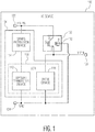
- Fig. 1 is a schematic block diagram of an IC device 100 in accordance with an embodiment of the invention.
- the IC device can be used in various applications, such as automotive applications, communications applications, industrial applications, medical applications, computer applications, and/or consumer or appliance applications.
- the IC device includes an NMOS device 102 and an ESD protection device 104 that is used to protect the NMOS device during an ESD event, which may be an ESD test or an actual ESD strike.
- the IC device can be implemented in a substrate, such as a semiconductor wafer.
- the IC device is packaged as a semiconductor IC chip.
- the IC device may be included in a microcontroller, which can be used for, for example, in vehicle control or communications, identification, wireless communications, and/or lighting control.
- the IC device is included in a computing device, such as a smartphone, a tablet computer, a laptop, etc.
- the IC device may be included in a Near Field Communications (NFC) capable computing device.
- NFC Near Field Communications
- the IC device is shown in Fig. 1 as including the NMOS device and the ESD protection device, in other embodiments, the IC device may include additional circuit elements.
- the IC device may include a control circuit that is located in a low voltage domain and used to control the NMOS device, which is located in a high voltage domain, and/or a drive circuit that is used to drive the NMOS device.
- the NMOS device 102 and the ESD protection device 104 are connected between first, second, and third nodes 122, 124, 126 through which one or more ESD pulses may be received.
- the first, second, and third nodes may be coupled to different voltages.
- the first, second, and third nodes may be implemented as electrical terminals of the IC device, such as electrical contact pads or electrical contact pins of the IC device.
- the first node is connected to a positive voltage and is referred to as a high voltage (HV) pin
- the third node is connected to a voltage that is lower than the voltage at the first node and is referred to as a low voltage (LV) pin
- the second node is connected to the ground and is referred to as a ground (GND) pin.
- HV high voltage
- LV low voltage
- GND ground
- the NMOS device 102 is susceptible to ESD strikes and is protected by the ESD protection device 104 in case of an ESD event.
- the NMOS device includes a source terminal, "S,” a gate terminal, "G,” a body, "B,” 132, and a drain terminal, "D.”
- the drain terminal, D, of the NMOS device is electrically connected to the first node 122
- the body, B, of the NMOS device is electrically connected to the second node 124
- the source terminal, S, of the NMOS device is electrically connected to the third node 126.
- the gate terminal, G, of the NMOS device may be electrically connected to a drive circuit that is used to generate a drive voltage for the NMOS device.
- the NMOS device can be implemented by at least one suitable semiconductor device.
- the NMOS device is an NMOS transistor.
- the NMOS device can be used in microcontrollers, transceivers, or switching circuits.
- the IC device may include serially connected diodes that are coupled in parallel with the NMOS device for current restriction and voltage surge protection.
- the ESD protection device 104 protects the NMOS device 102 during an ESD event.
- the ESD protection device can be used to protect a power supply domain of the IC device 100.
- the ESD protection device may be connected to a power supply rail of the IC device 100.
- the ESD protection device can be implemented by suitable semiconductor devices.
- the ESD protection device includes a bipolar transistor device 112, a series protection device 114, and a diode device 116.
- the ESD protection device is shown in Fig. 1 as including the bipolar transistor device, the series protection device, and the diode device, in other embodiments, the electrical device may include additional circuit elements.
- the ESD protection device may include one or more additional transistors and/or resistors.
- the bipolar transistor device 112 of the ESD protection device 104 is configured to shunt current in response to an ESD pulse.
- the bipolar transistor device is connected between the first node 122 and the second node 124.
- the bipolar transistor device can be implemented by at least one suitable semiconductor device.
- the bipolar transistor device is implemented by a bipolar transistor, which may be an NPN bipolar transistor or a PNP bipolar transistor.
- the series protection device 114 of the ESD protection device 104 is connected in series with the bipolar transistor device 112.
- the series protection device is used to maintain the hold voltage of the ESD protection device at a level that is suitable for latch up (e.g., allows latch-up safe operation of the IC device 100 up to its intended operating voltage (e.g., 3-5 V)).
- the hold voltage of the ESD protection device may be the snapback holding voltage at which a breakdown condition occurs in the ESD protection device.
- the series protection device is connected between the first node 122 and the bipolar transistor device.
- the series protection device is connected between the second node 124 and the bipolar transistor device.
- the series protection device can be implemented using at least one suitable semiconductor device.
- the series protection device is implemented using a bipolar transistor, which may be an NPN bipolar transistor or a PNP bipolar transistor.
- the series protection device is implemented using one or more diodes.
- the diode device 116 of the ESD protection device 104 is connected between the second node 124 and the third node 126.
- the diode device is connected to the source terminal, S, of the NMOS device 102 and to the third node.
- the diode device can be implemented using at least one suitable semiconductor device.
- the diode device is implemented using one or more diodes.
- the diode device 116 and the bipolar transistor device 112 are configured to form a parasitic silicon controlled rectifier (SCR) 118.
- the distance between the diode device and the bipolar transistor device is shorter than a predefined threshold.
- the diode device and the bipolar transistor device may be formed on the same substrate.
- the diode device overlaps with the bipolar transistor device.
- the diode device may be formed within the boundary (e.g., the packaging) of the bipolar transistor device.
- the diode device is formed within a substrate contact ring of the bipolar transistor device.
- the substrate contact ring may be made of one or more high electrical conductivity materials.
- the substrate contact ring includes one or more low resistance layers (e.g., silicided layers) formed on the surface of the ESD protection device 104 for better connection with other circuits.
- Figs. 2 and 3 illustrate two examples of ESD current paths through the ESD protection device 104 of the IC device 100 during an ESD event.
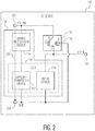
- Fig. 2 illustrates the ESD current path in the ESD protection device during an ESD pulse from the HV pin 122 to the GND pin 124.
- ESD current 220 flows through the series protection device 114 and the bipolar transistor device 112. Consequently, the SCR 118 formed by the diode device 116 and the bipolar transistor device 112 is not activated.
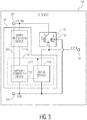
- Fig. 3 illustrates the ESD current path in the ESD protection device during an ESD pulse from the HV pin to the LV pin 126. As illustrated in Fig.
- ESD current 320 flows through the series protection device 114, the bipolar transistor device 112 and the diode device, which activates the SCR formed by the diode device and the bipolar transistor device. Activating the parasitic SCR causes the shorting of the bipolar transistor device, which results in an operating voltage that is lower than the operating voltage during an ESD pulse from the HV pin to GND.
- the NMOS device 102 may have a low fail voltage when stressed from the first node 122 to the third node 126 and a much higher fail voltage when stressed from the first node to the second node 124.
- the ESD protection device 104 depicted in Fig. 1 has a low operating voltage for ESD pulses received between the first node and the third node (e.g., lower than the fail voltage of the NMOS device) and allows a much higher DC stand-off voltage between the first node and the third node.
- the high DC stand-off voltage is beneficial for system robustness against over-voltages (e.g., a typical surge or a fault condition resulting in a DC voltage that is higher than intended operating voltage). Consequently, the ESD protection device provides adequate ESD protection for the NMOS device during an ESD strike from a high-voltage pin to a low-voltage pin as well as during an ESD strike from a high-voltage pin to the ground.
- Fig. 4 depicts an embodiment of the IC device 100 depicted in Fig. 1 .
- an IC device 400 includes an extended drain N-type MOSFET (EDNMOS) transistor 402 and an ESD protection device 404, which includes a first PNP bipolar transistor 412, a second PNP bipolar transistor 414, and a diode 416.
- the EDNMOS transistor includes a source terminal, "S,” a gate terminal, "G,” a body, "B,” 432, and a drain terminal, "D.”
- the EDNMOS transistor is configured as a source follower to create a low-voltage supply or is implemented in a data switch that is robust against high voltage.
- the drain terminal, D, of the EDNMOS transistor is electrically connected to a HV pin 422 and to the second PNP bipolar transistor
- the body, B, of the EDNMOS transistor is electrically connected to a ground (GND) pin 424, to the first PNP bipolar transistor, and to the diode
- the source terminal, S, of the EDNMOS transistor is electrically connected to a LV pin 426 and to the diode.
- NMOS device 102 is embodiments of the NMOS device 102, the ESD protection device 104, the bipolar transistor device 112, the series protection device 114, and the diode device 116 of the IC device 100 depicted in Fig. 1 , respectively.
- the IC device depicted in Fig. 4 is a possible implementation of the IC device 100 depicted in Fig. 1 .
- the IC device depicted in Fig. 1 can be implemented differently from the IC device depicted in Fig. 4 .
- the diode 416 and the first bipolar transistor 412 are configured to form a parasitic silicon controlled rectifier (SCR) 418.
- SCR parasitic silicon controlled rectifier
- the ESD protection device 404 when an ESD pulse is received between the HV pin and GND, ESD current flows through the second PNP bipolar transistor 414 and the first PNP bipolar transistor 412. Consequently, the SCR 418 formed by the diode and the first PNP bipolar transistor is not activated.
- ESD current flows through the second PNP bipolar transistor, the first PNP bipolar transistor, and the diode, which activates the SCR 418.
- the ESD protection device 404 can also meet latch-up safety requirements.
- the ESD protection device can be used for IC devices that operate at a relatively low operating voltage, but require a higher DC stand-off voltage for system robustness.
- Figs. 5-7 illustrate three examples of latch-up scenarios for the ESD protection device depicted in Fig. 4 .
- Fig. 5 illustrates a latch-up scenario for the ESD protection device where the HV pin is held at a normal operating voltage while a DC current (e.g., 100 mA) is pulled from the LV pin.
- the ESD protection device can withstand the latch-up scenario illustrated in Fig. 5 .
- the latch-up test voltage (e.g., the specified DC-stand-off voltage with respect to GND) at the HV pin is less than the sum of the hold voltages of the SCR and the second PNP bipolar transistor.
- the hold voltage of the SCR may be the snapback holding voltage at which a self-sustained current can flow in the SCR while the hold voltage of the second PNP bipolar transistor may be the snapback holding voltage at which a self-sustained current can flow in the second PNP bipolar transistor.
- the latch-up test voltage at the HV pin is limited to 13 V while the sum of the hold voltages of the SCR and the second PNP bipolar transistor is above 13 V.
- Fig. 6 illustrates a latch-up scenario for the ESD protection device 404 where an overvoltage is applied to the HV pin.
- the ESD protection device can withstand the latch-up scenario illustrated in Fig. 6 .
- the HV pin does not latch or sustain damage.
- the overvoltage can be limited to the Absolute Maximum Rating (AMR) listed for that HV pin.
- the latch-up test voltage e.g., the specified DC-stand-off voltage with respect to GND
- the latch-up test voltage at the HV pin is less than the sum of the hold voltages of the SCR and the second PNP bipolar transistor.
- the latch-up test voltage at the HV pin is limited to 26 V while the sum of the hold voltages of the SCR and the second PNP bipolar transistor is above 26 V.
- Fig. 7 illustrates a latch-up scenario for the ESD protection device where the HV pin is held at a normal operating voltage while a DC current (e.g., 100 mA) is pulled from an LV pin 756 that is not connected to the HV pin via the EDNMOS transistor 402.
- a DC current e.g. 100 mA
- the LV pin 756 is connected to the ground (GND) through a diode 746.
- the ESD protection device can withstand the latch-up scenario depicted in Fig. 7 .
- the latch-up test voltage (e.g., the specified DC-stand-off voltage with respect to GND) at the HV pin is less than the sum of the hold voltages of the SCR and the second PNP bipolar transistor.
- the latch-up test voltage at the HV pin is limited to 26 V while the sum of the hold voltages of the SCR and the second PNP bipolar transistor is above 26 V.
- Fig. 8 depicts an IC device 800 having three EDNMOS transistors 802-1, 802-2, 802-3 in accordance with an embodiment of the invention.
- the IC device includes three EDNMOS transistors 802-1, 802-2, 802-3 and an ESD protection device 804, which includes a first PNP bipolar transistor 812, a second PNP bipolar transistor 814, and three diodes 816-1, 816-2, 816-3.
- Each EDNMOS transistor includes a source terminal, "S,” a gate terminal, "G,” a body, "B,” 832-1, 832-2, or 832-3, and a drain terminal, "D.”
- S source terminal
- each EDNMOS transistor is electrically connected to a HV pin 822 and to the second PNP bipolar transistor
- the body, B, of each EDNMOS transistor is electrically connected to the ground (GND) pin 824, to the first PNP bipolar transistor, and to a respective diode
- the source terminal, S, of each EDNMOS transistor is electrically connected to an LV pin 826 and to a respective diode.
- NMOS device 102 is embodiments of the NMOS device 102, the ESD protection device 104, the bipolar transistor device 112, the series protection device 114, and the diode device 116 of the IC device 100 depicted in Fig. 1 , respectively.
- the IC device depicted in Fig. 8 is a possible implementation of the IC device 100 depicted in Fig. 1 .
- the IC device depicted in Fig. 1 can be implemented differently from the IC device depicted in Fig. 8 .
- the diode 816-1 and the first bipolar transistor 812 are configured to form a first parasitic SCR 818-1
- the diode 816-2 and the first bipolar transistor are configured to form a second parasitic SCR 818-2
- the diode 816-3 and the first bipolar transistor are configured to form a third parasitic SCR 818-3.
- ESD protection device 804 when an ESD pulse is received between the HV pin and GND, ESD current flows through the second PNP bipolar transistor 814 and the first PNP bipolar transistor 812. Consequently, the SCRs 818-1, 818-2, and 818-3 formed by the diodes and the first PNP bipolar transistor are not activated.
- ESD current flows through the second PNP bipolar transistor, the first PNP bipolar transistor, and a respective diode, which activates a respective SCR.
- Fig. 9 depicts an IC device 900 having two EDNMOS transistors 902-1, 902-2 in accordance with an embodiment of the invention.
- the IC device includes the two EDNMOS transistors and an ESD protection device 904, which includes a series diode 944, a first PNP bipolar transistor 912, a second PNP bipolar transistor 914, four diodes, "D_1b,” “D_2b,” “D_1t,” and “D_2t,” and an ESD railclamp 950.
- the ESD railclamp includes a combination of a bigFET and a trigger device for the bigFET.
- the ESD railclamp can be used to protect a supply domain of the IC device from sustaining damage (e.g., overheating or overvoltage) during an ESD strike by shunting the ESD current from the supply domain to the ground domain.
- damage e.g., overheating or overvoltage
- each EDNMOS transistor 902-1 or 902-2 includes a source terminal, "S,” a gate terminal, "G,” a body, “B,” 932-1, or 932-2, and a drain terminal, "D.”
- the drain terminal, D, of each EDNMOS transistor is electrically connected to a HV pin 922
- the body, B, of each EDNMOS transistor is electrically connected to the ground (GND) pin 924, to the first PNP bipolar transistor, and to a respective diode, D_1b, or D_2b
- the source terminal, S, of each EDNMOS transistor is electrically connected to an LV pin 826 and to respective diodes.
- the EDNMOS transistors, the ESD protection device 804, the first PNP bipolar transistor, the second PNP bipolar transistor, and the diodes of the IC device 900 depicted in Fig. 9 are embodiments of the NMOS device 102, the ESD protection device 104, the bipolar transistor device 112, the series protection device 114, and the diode device 116 of the IC device 100 depicted in Fig. 1 , respectively.
- the IC device depicted in Fig. 9 is a possible implementation of the IC device 100 depicted in Fig. 1 . However, the IC device depicted in Fig. 1 can be implemented differently from the IC device depicted in Fig. 9 .
- the diode D_1b and the first bipolar transistor 912 are configured to form a first parasitic SCR 918-1, and the diode D_2b and the first bipolar transistor are configured to form a second parasitic SCR 918-2.
- ESD protection device 904 when an ESD pulse is received between the HV pin and GND, ESD current flows through the series diode 944, the second PNP bipolar transistor 914, and the first PNP bipolar transistor 912. Consequently, the SCRs 918-1 and 918-2 formed by the diodes and the first PNP bipolar transistor are not activated.
- ESD protection device 904 has a relatively high operating voltage during an ESD pulse from the HV pin to GND and a lower operating voltage during an ESD pulse from the HV pin to the LV pin.
- Fig. 10 depicts a partial top layout view of the ESD protection device 904 depicted in Fig. 9 in accordance with an embodiment of the invention.
- the ESD protection device includes at least the series diode 944, the first PNP bipolar transistor 912, the second PNP bipolar transistor 914, and the four diodes, D_1b, D_2b, D_1t, and D_2t.
- the diodes, D_1b, D_2b overlap with the first PNP bipolar transistor 912 such that the substrate area of the diodes, D_1b, D_2b is part of the substrate area of the first PNP bipolar transistor 912.
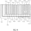
- Fig. 11 depicts a section of the partial ESD protection device 904 depicted in Fig. 10 .
- the first PNP bipolar transistor 912 includes collector components 1132-1, 1132-2, 1132-3, 1132-4, 1132-5, 1132-6, 1132-7, 1132-8, 1132-9, 1132-10, 1132-11, emitter components 1134-1, 1134-2, 1134-3, 1134-4, 1134-5, 1134-6, 1134-7, 1134-8, 1134-9, 1134-10, 1134-11 that are alternately located with respect to the collector components, a base structure 1136 and a substrate contact ring 1138.
- the substrate contact ring is used to capture holes that are accidentally injected into the substrate and/or ensure that the electric field inside the ESD protection device is contained within the edges of the ESD protection device, and does not affect neighboring semiconductor devices.
- the substrate contact ring forces zero potential around the edges of the ESD protection device such that there is no electric field protruding from the ESD protection device.
- the substrate contact ring may be made of one or more high electrical conductivity materials.
- the substrate contact ring may include low resistance layers (e.g., silicided layers) formed on the surface of the ESD protection device for better connection with other circuits.
- the diode, D_1b is formed within the substrate contact ring of the first PNP bipolar transistor 912 such that the substrate area of the diode, D_1b, is part of the substrate area of the substrate contact ring of the first PNP bipolar transistor 912. Because the diode, D_1b, is formed within the substrate contact ring of the first PNP bipolar transistor, the diode, D_1b, and the first PNP bipolar transistor form a parasitic silicon controlled rectifier (SCR).
- SCR parasitic silicon controlled rectifier
- Fig. 12 depicts a cross sectional view of the ESD protection device 904 depicted in Fig. 9 in accordance with an embodiment of the invention.
- the substrate contact ring 1138 and an active region 1244 are formed on top of (e.g., in direct contact with) a P-well region 1242 while an emitter region 1234 is formed on top of (e.g., in direct contact with) a base region 1236.
- Contact regions 1252, 1254, 1256 may be formed on top of (e.g., in direct contact with) the first active region, the second active region, and the emitter region, respectively.
- the contact regions 1252, 1254 may be connected to the ground pin 924 and to the LV pin 926 (shown in Fig. 9 ), respectively.
- the contact regions may include low resistance layers (e.g., silicided layers) formed on the surface of the ESD protection device for better connection with other circuits.
- Isolator regions e.g., shallow trench isolation regions filled with oxide or other isolation material
- the P-well region and the base region may be formed on top of (e.g., in direct contact with) a substrate 1258, which may be a silicon substrate region.
- the first PNP bipolar transistor 912 operates with a parasitic NPN bipolar transistor 1292 formed within the P-well region and the base region.
- Fig. 13 depicts another embodiment of the IC device 100 depicted in Fig. 1 .
- an IC device 1300 includes an EDNMOS transistor 1302 and an ESD protection device 1304, which includes a first PNP bipolar transistor 1312, a second PNP bipolar transistor 1314, and a diode 1316.
- a difference between the PNP bipolar transistor 1312 depicted in Fig. 13 and the PNP bipolar transistor 412 depicted in Fig. 4 is that a resistor 1334 is connected between the base and the emitter of the PNP bipolar transistor 1312.
- the EDNMOS transistor includes a source terminal, "S,” a gate terminal, "G,” a body, “B,” 432, and a drain terminal, "D.”
- S source terminal
- G gate terminal
- D drain terminal
- the drain terminal, D, of the EDNMOS transistor is electrically connected to a HV pin 1322 and to the second PNP bipolar transistor
- the body, B, of the EDNMOS transistor is electrically connected to a ground (GND) pin 1324, to the first PNP bipolar transistor, and to the diode
- the source terminal, S, of the EDNMOS transistor is electrically connected to a LV pin 1326 and to the diode.
- the diode 1316 and the first bipolar transistor 1312 form a parasitic silicon controlled rectifier (SCR) 1318.
- the EDNMOS transistor, the ESD protection device, the first PNP bipolar transistor, the second PNP bipolar transistor, and the diode of the IC device 400 depicted in Fig. 13 are embodiments of the NMOS device 102, the ESD protection device 104, the bipolar transistor device 112, the series protection device 114, and the diode device 116 of the IC device 100 depicted in Fig. 1 , respectively.
- the IC device depicted in Fig. 13 is a possible implementation of the IC device 100 depicted in Fig. 1 . However, the IC device depicted in Fig. 1 can be implemented differently from the IC device depicted in Fig. 13 .
- Fig. 14 is a process flow diagram that illustrates a method for operating an ESD protection device accordance with an embodiment of the invention.
- a first ESD pulse received between a first node and a second node is conducted using at least one bipolar transistor device connected between the first node and the second node.
- a drain terminal of an NMOS device to be protected is connectable to the first node, and a body of the NMOS device to be protected is connectable to the second node.
- a second ESD pulse received between the first node and a third node that is connectable to a source terminal of the NMOS device to be protected is conducted.
- a parasitic silicon controlled rectifier formed by one of the at least one bipolar transistor device and a diode device that is connected between the NMOS device to be protected and the third node is activated.
- the at least one bipolar transistor device may be the same as or similar to the bipolar transistor device 112 depicted in Fig. 1 , the PNP bipolar transistors 412, 414 depicted in Fig. 4 , the PNP bipolar transistors 812, 814 depicted in Fig. 8 , the PNP bipolar transistors 912, 914 depicted in Fig. 9 , and/or the PNP bipolar transistors 1312, 1314 depicted in Fig. 13 .
- the NMOS device to be protected may be the same as or similar to the NMOS device 102 depicted in Fig. 1 , the EDNMOS transistor 402 depicted in Fig. 4 , the EDNMOS transistors 802-1, 802-2, 802-3 depicted in Fig. 8 , the EDNMOS transistors 902-1, 902-2 depicted in Fig. 9 , and/or the EDNMOS transistor 1312 depicted in Fig. 13 .
- the diode device may be the same as or similar to the diode device 116 depicted in Fig. 1 , the diode 416 depicted in Fig. 4 , the diodes 816-1, 816-2, 816-3 depicted in Fig.
- the parasitic silicon controlled rectifier may be the same as or similar to the SCR 118 depicted in Fig. 1 , the SCR 418 depicted in Fig. 4 , the SCRs 818-1, 818-2, 818-3 depicted in Fig. 8 , the SCRs 918-1, 918-2 depicted in Fig. 9 , and/or the SCR 1318 depicted in Fig. 13 .
- an ESD protection device includes a bipolar transistor device connected between a first node and a second node, a series protection device connected in series with the bipolar transistor device, and a diode device connected between the second node and a third node.
- a drain terminal of an NMOS device to be protected is connectable to the first node.
- a body of the NMOS device to be protected is connectable to the second node.
- a source terminal of the NMOS device to be protected is connectable to the third node.
- the diode device and the bipolar transistor device are configured to form a parasitic silicon controlled rectifier. Other embodiments are also described.
Landscapes
- Engineering & Computer Science (AREA)
- Microelectronics & Electronic Packaging (AREA)
- Metal-Oxide And Bipolar Metal-Oxide Semiconductor Integrated Circuits (AREA)
- Semiconductor Integrated Circuits (AREA)
Abstract
Description
- Embodiments of the invention relate generally to electronic hardware and methods for operating electronic hardware, and, more particularly, to electrostatic discharge (ESD) protection devices and methods for operating an ESD protection device.
- An ESD protection device can be integrated into an integrated circuit (IC) chip to provide a low impedance channel to protect against thermal damage in the IC chip. During an ESD event such as an ESD strike or an ESD test, an ESD protection device shunts an ESD current pulse to protect a core circuit.
- Embodiments of an ESD protection device and a method of operating an ESD protection device are described. In one embodiment, an ESD protection device includes a bipolar transistor device connected between a first node and a second node, a series protection device connected in series with the bipolar transistor device, and a diode device connected between the second node and a third node. A drain terminal of an NMOS device to be protected is connectable to the first node. A body of the NMOS device to be protected is connectable to the second node. A source terminal of the NMOS device to be protected is connectable to the third node. The diode device and the bipolar transistor device are configured to form a parasitic silicon controlled rectifier (SCR). Other embodiments are also described.
- In an embodiment, a distance between the diode device and the bipolar transistor device is shorter than a predefined threshold.
- In an embodiment, the diode device overlaps with the bipolar transistor device.
- In an embodiment, the diode device is formed within a boundary of the bipolar transistor device.
- In an embodiment, the diode device is formed within a substrate contact ring of the bipolar transistor device.
- In an embodiment, the series protection device is connected to the first node, and the bipolar transistor device is connected to the second node.
- In an embodiment, the bipolar transistor device includes a PNP bipolar transistor or an NPN bipolar transistor.
- In an embodiment, the bipolar transistor device includes a resistor connected between an emitter of the bipolar transistor device and a base of the bipolar transistor device.
- In an embodiment, the series protection device includes a bipolar transistor or a diode.
- In an embodiment, the bipolar transistor includes a resistor connected between an emitter of the bipolar transistor and a base of the bipolar transistor.
- In an embodiment, the diode device includes at least one diode.
- In an embodiment, the parasitic silicon controlled rectifier is configured to be inactive in response to an ESD pulse received between the first node and the second node.
- In an embodiment, the parasitic silicon controlled rectifier is configured to be active in response to an ESD pulse received between the first node and the third node.
- In an embodiment, an integrated circuit (IC) device includes the ESD protection device and the NMOS device to be protected.
- In an embodiment, an ESD protection device includes a first PNP bipolar transistor connected between a first node and a second node, a second PNP bipolar transistor connected in series with the first PNP bipolar transistor, and a diode connected between the second node and a third node. A drain terminal of an NMOS device to be protected is connectable to the first node, a body of the NMOS device to be protected is connectable to the second node, and a source terminal of the NMOS device to be protected is connectable to the third node. The first PNP bipolar transistor and the diode are configured to form a parasitic silicon controlled rectifier. The diode is formed within a boundary of the first PNP bipolar transistor.
- In an embodiment, the diode is formed within a substrate contact ring of the first PNP bipolar transistor.
- In an embodiment, the second PNP bipolar transistor is connected to the first node, and the first PNP bipolar transistor is connected to the second node.
- In an embodiment, the parasitic silicon controlled rectifier is configured to be inactive in response to an ESD pulse received between the first node and the second node and to be active in response to an ESD pulse received between the first node and the third node.
- In an embodiment, the ESD protection device further includes a second diode connected to the first node and to the second PNP bipolar transistor.
- In an embodiment, a method for operating an ESD protection device involves conducting a first ESD pulse received between a first node and a second node using at least one bipolar transistor device connected between the first node and the second node, where a drain terminal of an NMOS device to be protected is connectable to the first node, and where a body of the NMOS device to be protected is connectable to the second node, and conducting a second ESD pulse received between the first node and a third node that is connectable to a source terminal of the NMOS device to be protected. Conducting the second ESD pulse involves activating a parasitic silicon controlled rectifier formed by the bipolar transistor device and a diode device that is connected between the NMOS device to be protected and the third node.
- Other aspects and advantages of embodiments of the present invention will become apparent from the following detailed description, taken in conjunction with the accompanying drawings, depicted by way of example of the principles of the invention.
-
-
Fig. 1 is a schematic block diagram of an IC device in accordance with an embodiment of the invention. -
Figs. 2 and3 illustrate two examples of ESD current paths through the ESD protection device of the IC device during an ESD event. -
Fig. 4 depicts an embodiment of the IC device depicted inFig. 1 . -
Figs. 5-7 illustrate three examples of test latch-up scenarios for the ESD protection device depicted inFig. 4 . -
Fig. 8 depicts an IC device having three extended drain N-type MOSFET (EDNMOS) transistors in accordance with an embodiment of the invention. -
Fig. 9 depicts an IC device having two EDNMOS transistors in accordance with an embodiment of the invention. -
Fig. 10 depicts a partial top layout view of the ESD protection device depicted inFig. 9 in accordance with an embodiment of the invention. -
Fig. 11 depicts a section of the partial ESD protection device depicted inFig. 10 . -
Fig. 12 depicts a cross sectional view of the ESD protection device depicted inFig. 9 in accordance with an embodiment of the invention. -
Fig. 13 depicts another embodiment of the IC device depicted inFig. 1 . -
Fig. 14 is a process flow diagram that illustrates a method for operating an ESD protection device in accordance with an embodiment of the invention. - Throughout the description, similar reference numbers may be used to identify similar elements.
- It will be readily understood that the components of the embodiments as generally described herein and illustrated in the appended figures could be arranged and designed in a wide variety of different configurations. Thus, the following detailed description of various embodiments, as represented in the figures, is not intended to limit the scope of the present disclosure, but is merely representative of various embodiments. While the various aspects of the embodiments are presented in drawings, the drawings are not necessarily drawn to scale unless specifically indicated.
- The described embodiments are to be considered in all respects only as illustrative and not restrictive. The scope of the invention is, therefore, indicated by the appended claims rather than by this detailed description. All changes which come within the meaning and range of equivalency of the claims are to be embraced within their scope.
- Reference throughout this specification to features, advantages, or similar language does not imply that all of the features and advantages that may be realized with the present invention should be or are in any single embodiment. Rather, language referring to the features and advantages is understood to mean that a specific feature, advantage, or characteristic described in connection with an embodiment is included in at least one embodiment. Thus, discussions of the features and advantages, and similar language, throughout this specification may, but do not necessarily, refer to the same embodiment.
- Furthermore, the described features, advantages, and characteristics of the invention may be combined in any suitable manner in one or more embodiments. One skilled in the relevant art will recognize, in light of the description herein, that the invention can be practiced without one or more of the specific features or advantages of a particular embodiment. In other instances, additional features and advantages may be recognized in certain embodiments that may not be present in all embodiments of the invention.
- Reference throughout this specification to "one embodiment," "an embodiment," or similar language means that a particular feature, structure, or characteristic described in connection with the indicated embodiment is included in at least one embodiment. Thus, the phrases "in one embodiment," "in an embodiment," and similar language throughout this specification may, but do not necessarily, all refer to the same embodiment.
-
Fig. 1 is a schematic block diagram of anIC device 100 in accordance with an embodiment of the invention. The IC device can be used in various applications, such as automotive applications, communications applications, industrial applications, medical applications, computer applications, and/or consumer or appliance applications. In the embodiment depicted inFig. 1 , the IC device includes anNMOS device 102 and anESD protection device 104 that is used to protect the NMOS device during an ESD event, which may be an ESD test or an actual ESD strike. The IC device can be implemented in a substrate, such as a semiconductor wafer. In an embodiment, the IC device is packaged as a semiconductor IC chip. The IC device may be included in a microcontroller, which can be used for, for example, in vehicle control or communications, identification, wireless communications, and/or lighting control. In some embodiments, the IC device is included in a computing device, such as a smartphone, a tablet computer, a laptop, etc. For example, the IC device may be included in a Near Field Communications (NFC) capable computing device. Although the IC device is shown inFig. 1 as including the NMOS device and the ESD protection device, in other embodiments, the IC device may include additional circuit elements. For example, the IC device may include a control circuit that is located in a low voltage domain and used to control the NMOS device, which is located in a high voltage domain, and/or a drive circuit that is used to drive the NMOS device. - In the embodiment depicted in
Fig. 1 , theNMOS device 102 and theESD protection device 104 are connected between first, second, andthird nodes - The
NMOS device 102 is susceptible to ESD strikes and is protected by theESD protection device 104 in case of an ESD event. In the embodiment depicted inFig. 1 , the NMOS device includes a source terminal, "S," a gate terminal, "G," a body, "B," 132, and a drain terminal, "D." In some embodiments, the drain terminal, D, of the NMOS device is electrically connected to thefirst node 122, the body, B, of the NMOS device is electrically connected to thesecond node 124, and the source terminal, S, of the NMOS device is electrically connected to thethird node 126. The gate terminal, G, of the NMOS device may be electrically connected to a drive circuit that is used to generate a drive voltage for the NMOS device. The NMOS device can be implemented by at least one suitable semiconductor device. In some embodiments, the NMOS device is an NMOS transistor. The NMOS device can be used in microcontrollers, transceivers, or switching circuits. In some embodiments, the IC device may include serially connected diodes that are coupled in parallel with the NMOS device for current restriction and voltage surge protection. - The
ESD protection device 104 protects theNMOS device 102 during an ESD event. The ESD protection device can be used to protect a power supply domain of theIC device 100. For example, the ESD protection device may be connected to a power supply rail of theIC device 100. The ESD protection device can be implemented by suitable semiconductor devices. In the embodiment depicted inFig. 1 , the ESD protection device includes abipolar transistor device 112, aseries protection device 114, and adiode device 116. Although the ESD protection device is shown inFig. 1 as including the bipolar transistor device, the series protection device, and the diode device, in other embodiments, the electrical device may include additional circuit elements. For example, the ESD protection device may include one or more additional transistors and/or resistors. - The
bipolar transistor device 112 of theESD protection device 104 is configured to shunt current in response to an ESD pulse. In the embodiment depicted inFig. 1 , the bipolar transistor device is connected between thefirst node 122 and thesecond node 124. The bipolar transistor device can be implemented by at least one suitable semiconductor device. In some embodiments, the bipolar transistor device is implemented by a bipolar transistor, which may be an NPN bipolar transistor or a PNP bipolar transistor. - The
series protection device 114 of theESD protection device 104 is connected in series with thebipolar transistor device 112. The series protection device is used to maintain the hold voltage of the ESD protection device at a level that is suitable for latch up (e.g., allows latch-up safe operation of theIC device 100 up to its intended operating voltage (e.g., 3-5 V)). The hold voltage of the ESD protection device may be the snapback holding voltage at which a breakdown condition occurs in the ESD protection device. In the embodiment depicted inFig. 1 , the series protection device is connected between thefirst node 122 and the bipolar transistor device. In some embodiments, the series protection device is connected between thesecond node 124 and the bipolar transistor device. The series protection device can be implemented using at least one suitable semiconductor device. In some embodiments, the series protection device is implemented using a bipolar transistor, which may be an NPN bipolar transistor or a PNP bipolar transistor. In some other embodiments, the series protection device is implemented using one or more diodes. - The
diode device 116 of theESD protection device 104 is connected between thesecond node 124 and thethird node 126. In the embodiment depicted inFig. 1 , the diode device is connected to the source terminal, S, of theNMOS device 102 and to the third node. The diode device can be implemented using at least one suitable semiconductor device. For example, the diode device is implemented using one or more diodes. - In the embodiment depicted in
Fig. 1 , thediode device 116 and thebipolar transistor device 112 are configured to form a parasitic silicon controlled rectifier (SCR) 118. In some embodiments, the distance between the diode device and the bipolar transistor device is shorter than a predefined threshold. The diode device and the bipolar transistor device may be formed on the same substrate. In some embodiments, the diode device overlaps with the bipolar transistor device. For example, the diode device may be formed within the boundary (e.g., the packaging) of the bipolar transistor device. In some embodiments, the diode device is formed within a substrate contact ring of the bipolar transistor device. The substrate contact ring may be made of one or more high electrical conductivity materials. In an embodiment, the substrate contact ring includes one or more low resistance layers (e.g., silicided layers) formed on the surface of theESD protection device 104 for better connection with other circuits. -
Figs. 2 and3 illustrate two examples of ESD current paths through theESD protection device 104 of theIC device 100 during an ESD event. Specifically,Fig. 2 illustrates the ESD current path in the ESD protection device during an ESD pulse from theHV pin 122 to theGND pin 124. As illustrated inFig. 2 , when an ESD pulse is received between the HV pin and GND, ESD current 220 flows through theseries protection device 114 and thebipolar transistor device 112. Consequently, theSCR 118 formed by thediode device 116 and thebipolar transistor device 112 is not activated.Fig. 3 illustrates the ESD current path in the ESD protection device during an ESD pulse from the HV pin to theLV pin 126. As illustrated inFig. 3 , when an ESD pulse is received between the HV pin and the LV pin, ESD current 320 flows through theseries protection device 114, thebipolar transistor device 112 and the diode device, which activates the SCR formed by the diode device and the bipolar transistor device. Activating the parasitic SCR causes the shorting of the bipolar transistor device, which results in an operating voltage that is lower than the operating voltage during an ESD pulse from the HV pin to GND. - The
NMOS device 102 may have a low fail voltage when stressed from thefirst node 122 to thethird node 126 and a much higher fail voltage when stressed from the first node to thesecond node 124. TheESD protection device 104 depicted inFig. 1 has a low operating voltage for ESD pulses received between the first node and the third node (e.g., lower than the fail voltage of the NMOS device) and allows a much higher DC stand-off voltage between the first node and the third node. The high DC stand-off voltage is beneficial for system robustness against over-voltages (e.g., a typical surge or a fault condition resulting in a DC voltage that is higher than intended operating voltage). Consequently, the ESD protection device provides adequate ESD protection for the NMOS device during an ESD strike from a high-voltage pin to a low-voltage pin as well as during an ESD strike from a high-voltage pin to the ground. -
Fig. 4 depicts an embodiment of theIC device 100 depicted inFig. 1 . In the embodiment depicted inFig. 4 , anIC device 400 includes an extended drain N-type MOSFET (EDNMOS)transistor 402 and anESD protection device 404, which includes a first PNPbipolar transistor 412, a second PNPbipolar transistor 414, and adiode 416. The EDNMOS transistor includes a source terminal, "S," a gate terminal, "G," a body, "B," 432, and a drain terminal, "D." In some embodiments, the EDNMOS transistor is configured as a source follower to create a low-voltage supply or is implemented in a data switch that is robust against high voltage. In the embodiment depicted inFig. 4 , the drain terminal, D, of the EDNMOS transistor is electrically connected to aHV pin 422 and to the second PNP bipolar transistor, the body, B, of the EDNMOS transistor is electrically connected to a ground (GND)pin 424, to the first PNP bipolar transistor, and to the diode, and the source terminal, S, of the EDNMOS transistor is electrically connected to aLV pin 426 and to the diode. The EDNMOS transistor, theESD protection device 404, the first PNP bipolar transistor, the second PNP bipolar transistor, and the diode of theIC device 400 depicted inFig. 4 are embodiments of theNMOS device 102, theESD protection device 104, thebipolar transistor device 112, theseries protection device 114, and thediode device 116 of theIC device 100 depicted inFig. 1 , respectively. The IC device depicted inFig. 4 is a possible implementation of theIC device 100 depicted inFig. 1 . However, the IC device depicted inFig. 1 can be implemented differently from the IC device depicted inFig. 4 . - In the embodiment depicted in
Fig. 4 , thediode 416 and the firstbipolar transistor 412 are configured to form a parasitic silicon controlled rectifier (SCR) 418. In an example operation of theESD protection device 404, when an ESD pulse is received between the HV pin and GND, ESD current flows through the second PNPbipolar transistor 414 and the first PNPbipolar transistor 412. Consequently, theSCR 418 formed by the diode and the first PNP bipolar transistor is not activated. In addition, when an ESD pulse is received between the HV pin and the LV pin, ESD current flows through the second PNP bipolar transistor, the first PNP bipolar transistor, and the diode, which activates theSCR 418. - In addition to providing ESD protection for the
EDNMOS transistor 402, theESD protection device 404 can also meet latch-up safety requirements. The ESD protection device can be used for IC devices that operate at a relatively low operating voltage, but require a higher DC stand-off voltage for system robustness.Figs. 5-7 illustrate three examples of latch-up scenarios for the ESD protection device depicted inFig. 4 . In particular,Fig. 5 illustrates a latch-up scenario for the ESD protection device where the HV pin is held at a normal operating voltage while a DC current (e.g., 100 mA) is pulled from the LV pin. The ESD protection device can withstand the latch-up scenario illustrated inFig. 5 . In particular, in theESD protection device 404, the latch-up test voltage (e.g., the specified DC-stand-off voltage with respect to GND) at the HV pin is less than the sum of the hold voltages of the SCR and the second PNP bipolar transistor. The hold voltage of the SCR may be the snapback holding voltage at which a self-sustained current can flow in the SCR while the hold voltage of the second PNP bipolar transistor may be the snapback holding voltage at which a self-sustained current can flow in the second PNP bipolar transistor. For example, the latch-up test voltage at the HV pin is limited to 13 V while the sum of the hold voltages of the SCR and the second PNP bipolar transistor is above 13 V. -
Fig. 6 illustrates a latch-up scenario for theESD protection device 404 where an overvoltage is applied to the HV pin. The ESD protection device can withstand the latch-up scenario illustrated inFig. 6 . In particular, in theESD protection device 404, the HV pin does not latch or sustain damage. The overvoltage can be limited to the Absolute Maximum Rating (AMR) listed for that HV pin. The latch-up test voltage (e.g., the specified DC-stand-off voltage with respect to GND) at the HV pin is less than the sum of the hold voltages of the SCR and the second PNP bipolar transistor. For example, the latch-up test voltage at the HV pin is limited to 26 V while the sum of the hold voltages of the SCR and the second PNP bipolar transistor is above 26 V. -
Fig. 7 illustrates a latch-up scenario for the ESD protection device where the HV pin is held at a normal operating voltage while a DC current (e.g., 100 mA) is pulled from anLV pin 756 that is not connected to the HV pin via theEDNMOS transistor 402. In the latch-up scenario illustrated inFig. 7 , theLV pin 756 is connected to the ground (GND) through adiode 746. The ESD protection device can withstand the latch-up scenario depicted inFig. 7 . In particular, in theESD protection device 404, the latch-up test voltage (e.g., the specified DC-stand-off voltage with respect to GND) at the HV pin is less than the sum of the hold voltages of the SCR and the second PNP bipolar transistor. For example, the latch-up test voltage at the HV pin is limited to 26 V while the sum of the hold voltages of the SCR and the second PNP bipolar transistor is above 26 V. -
Fig. 8 depicts anIC device 800 having three EDNMOS transistors 802-1, 802-2, 802-3 in accordance with an embodiment of the invention. In the embodiment depicted inFig. 8 , the IC device includes three EDNMOS transistors 802-1, 802-2, 802-3 and anESD protection device 804, which includes a first PNPbipolar transistor 812, a second PNPbipolar transistor 814, and three diodes 816-1, 816-2, 816-3. Each EDNMOS transistor includes a source terminal, "S," a gate terminal, "G," a body, "B," 832-1, 832-2, or 832-3, and a drain terminal, "D." In the embodiment depicted inFig. 8 , the drain terminal, D, of each EDNMOS transistor is electrically connected to aHV pin 822 and to the second PNP bipolar transistor, the body, B, of each EDNMOS transistor is electrically connected to the ground (GND)pin 824, to the first PNP bipolar transistor, and to a respective diode, and the source terminal, S, of each EDNMOS transistor is electrically connected to an LV pin 826 and to a respective diode. The EDNMOS transistors, theESD protection device 804, the first PNP bipolar transistor, the second PNP bipolar transistor, and the diodes of theIC device 800 depicted inFig. 8 are embodiments of theNMOS device 102, theESD protection device 104, thebipolar transistor device 112, theseries protection device 114, and thediode device 116 of theIC device 100 depicted inFig. 1 , respectively. The IC device depicted inFig. 8 is a possible implementation of theIC device 100 depicted inFig. 1 . However, the IC device depicted inFig. 1 can be implemented differently from the IC device depicted inFig. 8 . - In the embodiment depicted in
Fig. 8 , the diode 816-1 and the firstbipolar transistor 812 are configured to form a first parasitic SCR 818-1, the diode 816-2 and the first bipolar transistor are configured to form a second parasitic SCR 818-2, and the diode 816-3 and the first bipolar transistor are configured to form a third parasitic SCR 818-3. In an example operation of theESD protection device 804, when an ESD pulse is received between the HV pin and GND, ESD current flows through the second PNPbipolar transistor 814 and the first PNPbipolar transistor 812. Consequently, the SCRs 818-1, 818-2, and 818-3 formed by the diodes and the first PNP bipolar transistor are not activated. In addition, when an ESD pulse is received between the HV pin and a respective LV pin, ESD current flows through the second PNP bipolar transistor, the first PNP bipolar transistor, and a respective diode, which activates a respective SCR. -
Fig. 9 depicts anIC device 900 having two EDNMOS transistors 902-1, 902-2 in accordance with an embodiment of the invention. In the embodiment depicted inFig. 9 , the IC device includes the two EDNMOS transistors and anESD protection device 904, which includes aseries diode 944, a first PNPbipolar transistor 912, a second PNPbipolar transistor 914, four diodes, "D_1b," "D_2b," "D_1t," and "D_2t," and anESD railclamp 950. In some embodiments, the ESD railclamp includes a combination of a bigFET and a trigger device for the bigFET. The ESD railclamp can be used to protect a supply domain of the IC device from sustaining damage (e.g., overheating or overvoltage) during an ESD strike by shunting the ESD current from the supply domain to the ground domain. In the embodiment depicted inFig. 9 , each EDNMOS transistor 902-1 or 902-2 includes a source terminal, "S," a gate terminal, "G," a body, "B," 932-1, or 932-2, and a drain terminal, "D." The drain terminal, D, of each EDNMOS transistor is electrically connected to aHV pin 922, the body, B, of each EDNMOS transistor is electrically connected to the ground (GND)pin 924, to the first PNP bipolar transistor, and to a respective diode, D_1b, or D_2b, and the source terminal, S, of each EDNMOS transistor is electrically connected to an LV pin 826 and to respective diodes. The EDNMOS transistors, theESD protection device 804, the first PNP bipolar transistor, the second PNP bipolar transistor, and the diodes of theIC device 900 depicted inFig. 9 are embodiments of theNMOS device 102, theESD protection device 104, thebipolar transistor device 112, theseries protection device 114, and thediode device 116 of theIC device 100 depicted inFig. 1 , respectively. The IC device depicted inFig. 9 is a possible implementation of theIC device 100 depicted inFig. 1 . However, the IC device depicted inFig. 1 can be implemented differently from the IC device depicted inFig. 9 . - In the embodiment depicted in
Fig. 9 , the diode D_1b and the firstbipolar transistor 912 are configured to form a first parasitic SCR 918-1, and the diode D_2b and the first bipolar transistor are configured to form a second parasitic SCR 918-2. In an example operation of theESD protection device 904, when an ESD pulse is received between the HV pin and GND, ESD current flows through theseries diode 944, the second PNPbipolar transistor 914, and the first PNPbipolar transistor 912. Consequently, the SCRs 918-1 and 918-2 formed by the diodes and the first PNP bipolar transistor are not activated. In addition, when an ESD pulse is received between the HV pin and a respective LV pin, ESD current flows through the series diode, the second PNP bipolar transistor, the first PNP bipolar transistor, and respective diodes, which activates a respective SCR. TheESD protection device 904 has a relatively high operating voltage during an ESD pulse from the HV pin to GND and a lower operating voltage during an ESD pulse from the HV pin to the LV pin. -
Fig. 10 depicts a partial top layout view of theESD protection device 904 depicted inFig. 9 in accordance with an embodiment of the invention. In the partial top layout view depicted inFig. 10 , the ESD protection device includes at least theseries diode 944, the first PNPbipolar transistor 912, the second PNPbipolar transistor 914, and the four diodes, D_1b, D_2b, D_1t, and D_2t. The diodes, D_1b, D_2b, overlap with the first PNPbipolar transistor 912 such that the substrate area of the diodes, D_1b, D_2b is part of the substrate area of the first PNPbipolar transistor 912. -
Fig. 11 depicts a section of the partialESD protection device 904 depicted inFig. 10 . In the section depicted inFig. 11 , the first PNPbipolar transistor 912 includes collector components 1132-1, 1132-2, 1132-3, 1132-4, 1132-5, 1132-6, 1132-7, 1132-8, 1132-9, 1132-10, 1132-11, emitter components 1134-1, 1134-2, 1134-3, 1134-4, 1134-5, 1134-6, 1134-7, 1134-8, 1134-9, 1134-10, 1134-11 that are alternately located with respect to the collector components, abase structure 1136 and asubstrate contact ring 1138. In some embodiments, the substrate contact ring is used to capture holes that are accidentally injected into the substrate and/or ensure that the electric field inside the ESD protection device is contained within the edges of the ESD protection device, and does not affect neighboring semiconductor devices. For example, the substrate contact ring forces zero potential around the edges of the ESD protection device such that there is no electric field protruding from the ESD protection device. The substrate contact ring may be made of one or more high electrical conductivity materials. The substrate contact ring may include low resistance layers (e.g., silicided layers) formed on the surface of the ESD protection device for better connection with other circuits. The diode, D_1b, is formed within the substrate contact ring of the first PNPbipolar transistor 912 such that the substrate area of the diode, D_1b, is part of the substrate area of the substrate contact ring of the first PNPbipolar transistor 912. Because the diode, D_1b, is formed within the substrate contact ring of the first PNP bipolar transistor, the diode, D_1b, and the first PNP bipolar transistor form a parasitic silicon controlled rectifier (SCR). -
Fig. 12 depicts a cross sectional view of theESD protection device 904 depicted inFig. 9 in accordance with an embodiment of the invention. In the cross-sectional view ofFig. 12 , thesubstrate contact ring 1138 and anactive region 1244 are formed on top of (e.g., in direct contact with) a P-well region 1242 while anemitter region 1234 is formed on top of (e.g., in direct contact with) abase region 1236. Contactregions contact regions ground pin 924 and to the LV pin 926 (shown inFig. 9 ), respectively. The contact regions may include low resistance layers (e.g., silicided layers) formed on the surface of the ESD protection device for better connection with other circuits. Isolator regions (e.g., shallow trench isolation regions filled with oxide or other isolation material) 1262, 1264, 1266 are formed on top of (e.g., in direct contact with) the P-well region and the base region, respectively. The P-well region and the base region may be formed on top of (e.g., in direct contact with) a substrate 1258, which may be a silicon substrate region. As shown inFig. 12 , the first PNPbipolar transistor 912 operates with a parasitic NPNbipolar transistor 1292 formed within the P-well region and the base region. -
Fig. 13 depicts another embodiment of theIC device 100 depicted inFig. 1 . In the embodiment depicted inFig. 4 , anIC device 1300 includes anEDNMOS transistor 1302 and anESD protection device 1304, which includes a first PNPbipolar transistor 1312, a second PNPbipolar transistor 1314, and adiode 1316. A difference between the PNPbipolar transistor 1312 depicted inFig. 13 and the PNPbipolar transistor 412 depicted inFig. 4 is that aresistor 1334 is connected between the base and the emitter of the PNPbipolar transistor 1312. A difference between the PNPbipolar transistor 1314 depicted inFig. 13 and the PNPbipolar transistor 414 depicted inFig. 4 is that aresistor 1336 is connected between the base and the emitter of the PNPbipolar transistor 1314. The EDNMOS transistor includes a source terminal, "S," a gate terminal, "G," a body, "B," 432, and a drain terminal, "D." In the embodiment depicted inFig. 13 , the drain terminal, D, of the EDNMOS transistor is electrically connected to aHV pin 1322 and to the second PNP bipolar transistor, the body, B, of the EDNMOS transistor is electrically connected to a ground (GND)pin 1324, to the first PNP bipolar transistor, and to the diode, and the source terminal, S, of the EDNMOS transistor is electrically connected to aLV pin 1326 and to the diode. In the embodiment depicted inFig. 13 , thediode 1316 and the firstbipolar transistor 1312 form a parasitic silicon controlled rectifier (SCR) 1318. The EDNMOS transistor, the ESD protection device, the first PNP bipolar transistor, the second PNP bipolar transistor, and the diode of theIC device 400 depicted inFig. 13 are embodiments of theNMOS device 102, theESD protection device 104, thebipolar transistor device 112, theseries protection device 114, and thediode device 116 of theIC device 100 depicted inFig. 1 , respectively. The IC device depicted inFig. 13 is a possible implementation of theIC device 100 depicted inFig. 1 . However, the IC device depicted inFig. 1 can be implemented differently from the IC device depicted inFig. 13 . -
Fig. 14 is a process flow diagram that illustrates a method for operating an ESD protection device accordance with an embodiment of the invention. Atblock 1402, a first ESD pulse received between a first node and a second node is conducted using at least one bipolar transistor device connected between the first node and the second node. A drain terminal of an NMOS device to be protected is connectable to the first node, and a body of the NMOS device to be protected is connectable to the second node. Atblock 1404, a second ESD pulse received between the first node and a third node that is connectable to a source terminal of the NMOS device to be protected is conducted. A parasitic silicon controlled rectifier formed by one of the at least one bipolar transistor device and a diode device that is connected between the NMOS device to be protected and the third node is activated. The at least one bipolar transistor device may be the same as or similar to thebipolar transistor device 112 depicted inFig. 1 , the PNPbipolar transistors Fig. 4 , the PNPbipolar transistors Fig. 8 , the PNPbipolar transistors Fig. 9 , and/or the PNPbipolar transistors Fig. 13 . The NMOS device to be protected may be the same as or similar to theNMOS device 102 depicted inFig. 1 , theEDNMOS transistor 402 depicted inFig. 4 , the EDNMOS transistors 802-1, 802-2, 802-3 depicted inFig. 8 , the EDNMOS transistors 902-1, 902-2 depicted inFig. 9 , and/or theEDNMOS transistor 1312 depicted inFig. 13 . The diode device may be the same as or similar to thediode device 116 depicted inFig. 1 , thediode 416 depicted inFig. 4 , the diodes 816-1, 816-2, 816-3 depicted inFig. 8 , the diodes D_1b, D_2b depicted inFig. 9 , and/or thediode 1316 depicted inFig. 13 . The parasitic silicon controlled rectifier may be the same as or similar to theSCR 118 depicted inFig. 1 , theSCR 418 depicted inFig. 4 , the SCRs 818-1, 818-2, 818-3 depicted inFig. 8 , the SCRs 918-1, 918-2 depicted inFig. 9 , and/or theSCR 1318 depicted inFig. 13 . - Embodiments of an electrostatic discharge (ESD) protection device and a method of operating an ESD protection device are described. In one embodiment, an ESD protection device includes a bipolar transistor device connected between a first node and a second node, a series protection device connected in series with the bipolar transistor device, and a diode device connected between the second node and a third node. A drain terminal of an NMOS device to be protected is connectable to the first node. A body of the NMOS device to be protected is connectable to the second node. A source terminal of the NMOS device to be protected is connectable to the third node. The diode device and the bipolar transistor device are configured to form a parasitic silicon controlled rectifier. Other embodiments are also described.
- Although the operations of the method herein are shown and described in a particular order, the order of the operations of the method may be altered so that certain operations may be performed in an inverse order or so that certain operations may be performed, at least in part, concurrently with other operations. In another embodiment, instructions or sub-operations of distinct operations may be implemented in an intermittent and/or alternating manner.
- In addition, although specific embodiments of the invention that have been described or depicted include several components described or depicted herein, other embodiments of the invention may include fewer or more components to implement less or more features.
- Furthermore, although specific embodiments of the invention have been described and depicted, the invention is not to be limited to the specific forms or arrangements of parts so described and depicted. The scope of the invention is to be defined by the claims appended hereto and their equivalents.
Claims (15)
- An electrostatic discharge (ESD) protection device, the ESD protection device comprising:a bipolar transistor device connected between a first node and a second node, wherein a drain terminal of an NMOS device to be protected is connectable to the first node, and wherein a body of the NMOS device to be protected is connectable to the second node;a series protection device connected in series with the bipolar transistor device; anda diode device connected between the second node and a third node, wherein a source terminal of the NMOS device to be protected is connectable to the third node;wherein the diode device and the bipolar transistor device are configured to form a parasitic silicon controlled rectifier.
- The ESD protection device of claim 1, wherein a distance between the diode device and the bipolar transistor device is shorter than a predefined threshold.
- The ESD protection device of claim 1 or 2, wherein the diode device overlaps with the bipolar transistor device.
- The ESD protection device of any preceding claim, wherein the diode device is formed within a boundary of the bipolar transistor device.
- The ESD protection device of any preceding claim, wherein the diode device is formed within a substrate contact ring of the bipolar transistor device.
- The ESD protection device of any preceding claim, wherein the series protection device is connected to the first node, and wherein the bipolar transistor device is connected to the second node.
- The ESD protection device of any preceding claim, wherein the bipolar transistor device comprises a PNP bipolar transistor or an NPN bipolar transistor.
- The ESD protection device of any preceding claim, wherein the bipolar transistor device comprises a resistor connected between an emitter of the bipolar transistor device and a base of the bipolar transistor device.
- The ESD protection device of any preceding claim, wherein the series protection device comprises a bipolar transistor or a diode.
- The ESD protection device of any preceding claim, wherein the bipolar transistor comprises a resistor connected between an emitter of the bipolar transistor and a base of the bipolar transistor.
- The ESD protection device of any preceding claim, wherein the diode device comprises at least one diode.
- The ESD protection device of any preceding claim, wherein the parasitic silicon controlled rectifier is configured to be inactive in response to an ESD pulse received between the first node and the second node.
- The ESD protection device of any of claims 1 to 11, wherein the parasitic silicon controlled rectifier is configured to be active in response to an ESD pulse received between the first node and the third node.
- An integrated circuit (IC) device comprising the ESD protection device of any preceding claim and the NMOS device to be protected.
- A method for operating an electrostatic discharge (ESD) protection device, the method comprising:conducting a first ESD pulse received between a first node and a second node using at least one bipolar transistor device connected between the first node and the second node, wherein a drain terminal of an NMOS device to be protected is connectable to the first node, and wherein a body of the NMOS device to be protected is connectable to the second node; andconducting a second ESD pulse received between the first node and a third node that is connectable to a source terminal of the NMOS device to be protected, wherein conducting the second ESD pulse comprises activating a parasitic silicon controlled rectifier formed by the bipolar transistor device and a diode device that is connected between the NMOS device to be protected and the third node.
Applications Claiming Priority (1)
| Application Number | Priority Date | Filing Date | Title |
|---|---|---|---|
| US15/595,068 US10366974B2 (en) | 2017-05-15 | 2017-05-15 | Electrostatic discharge (ESD) protection device and method for operating an ESD protection device |
Publications (2)
| Publication Number | Publication Date |
|---|---|
| EP3404713A1 true EP3404713A1 (en) | 2018-11-21 |
| EP3404713B1 EP3404713B1 (en) | 2022-08-17 |
Family
ID=62167126
Family Applications (1)
| Application Number | Title | Priority Date | Filing Date |
|---|---|---|---|
| EP18171626.7A Active EP3404713B1 (en) | 2017-05-15 | 2018-05-09 | Electrostatic discharge (esd) protection device and method for operating an esd protection device |
Country Status (3)
| Country | Link |
|---|---|
| US (1) | US10366974B2 (en) |
| EP (1) | EP3404713B1 (en) |
| CN (1) | CN108878403B (en) |
Families Citing this family (7)
| Publication number | Priority date | Publication date | Assignee | Title |
|---|---|---|---|---|
| US10381340B2 (en) * | 2016-01-26 | 2019-08-13 | Nxp B.V. | Electrostatic discharge protection with integrated diode |
| KR20190140216A (en) * | 2018-06-11 | 2019-12-19 | 에스케이하이닉스 주식회사 | Semiconductor Integrated Circuit Device Including Circuit for Protecting Electro- Static Discharge |
| US10978444B2 (en) * | 2018-09-19 | 2021-04-13 | Nxp B.V. | RC-triggered bracing circuit |
| US11133299B2 (en) * | 2018-10-04 | 2021-09-28 | Nxp B.V. | Gate-lifted NMOS ESD protection device |
| US11532610B2 (en) | 2020-06-24 | 2022-12-20 | Amazing Microelectronic Corp. | Electrostatic discharge protection structure and electrostatic discharge protection circuit with low parasitic capacitance thereof |
| EP4213209B1 (en) | 2022-01-12 | 2025-12-24 | Nexperia B.V. | Esd protection device |
| US12484311B2 (en) | 2022-09-29 | 2025-11-25 | Nxp B.V. | ESD clamp circuit with vertical bipolar transistor |
Citations (3)
| Publication number | Priority date | Publication date | Assignee | Title |
|---|---|---|---|---|
| US20100044834A1 (en) * | 2008-08-20 | 2010-02-25 | Jae-Young Park | Electrostatic discharge protection circuit |
| US20140167104A1 (en) * | 2012-12-19 | 2014-06-19 | Analog Devices, Inc. | Interface protection device with integrated supply clamp and method of forming the same |
| EP3107122A1 (en) * | 2015-06-17 | 2016-12-21 | Nxp B.V. | An electrostatic discharge protection device |
Family Cites Families (17)
| Publication number | Priority date | Publication date | Assignee | Title |
|---|---|---|---|---|
| US5359211A (en) * | 1991-07-18 | 1994-10-25 | Harris Corporation | High voltage protection using SCRs |
| US5754381A (en) * | 1997-02-04 | 1998-05-19 | Industrial Technology Research Institute | Output ESD protection with high-current-triggered lateral SCR |
| US6825504B2 (en) * | 1999-05-03 | 2004-11-30 | Hitachi, Ltd. | Semiconductor integrated circuit device and method of manufacturing the same |
| US6512662B1 (en) | 1999-11-30 | 2003-01-28 | Illinois Institute Of Technology | Single structure all-direction ESD protection for integrated circuits |
| US7548401B2 (en) * | 2001-03-16 | 2009-06-16 | Sarnoff Corporation | Electrostatic discharge protection structures for high speed technologies with mixed and ultra-low voltage supplies |
| US6894881B1 (en) | 2002-02-19 | 2005-05-17 | National Semiconductor Corp | ESD protection methods and devices using additional terminal in the diode structures |
| US7154724B2 (en) * | 2004-03-29 | 2006-12-26 | Taiwan Semiconductor Manufacturing Co., Ltd | Output buffer ESD protection using parasitic SCR protection circuit for CMOS VLSI integrated circuits |
| JP4515822B2 (en) * | 2004-05-25 | 2010-08-04 | 株式会社東芝 | Electrostatic protection circuit and semiconductor integrated circuit device using the same |
| CN101142729B (en) * | 2005-03-30 | 2011-11-16 | 索菲克斯公司 | Semiconductor device based on a SCR |
| JP2008021852A (en) * | 2006-07-13 | 2008-01-31 | Toshiba Corp | Semiconductor device |
| US9202938B2 (en) * | 2006-11-30 | 2015-12-01 | Alpha And Omega Semiconductor Incorporated | Latch-up free vertical TVS diode array structure using trench isolation |
| JP4245644B1 (en) * | 2007-11-21 | 2009-03-25 | シャープ株式会社 | Electrostatic discharge protection device and semiconductor integrated circuit having the same |
| CN101938119B (en) * | 2009-06-30 | 2014-01-15 | 万国半导体股份有限公司 | Transient voltage suppressor (TVS) with improved clamping voltage |
| JP5540801B2 (en) * | 2010-03-19 | 2014-07-02 | 富士通セミコンダクター株式会社 | ESD protection circuit and semiconductor device |
| WO2013083767A1 (en) * | 2011-12-08 | 2013-06-13 | Sofics Bvba | A high holding voltage, mixed-voltage domain electrostatic discharge clamp |
| US8913358B2 (en) * | 2012-06-27 | 2014-12-16 | Globalfoundries Singapore Pte. Ltd. | Latch-up immune ESD protection |
| JP2015032767A (en) * | 2013-08-06 | 2015-02-16 | 株式会社日立製作所 | Semiconductor device |
-
2017
- 2017-05-15 US US15/595,068 patent/US10366974B2/en active Active
-
2018
- 2018-05-09 EP EP18171626.7A patent/EP3404713B1/en active Active
- 2018-05-15 CN CN201810464729.2A patent/CN108878403B/en active Active
Patent Citations (3)
| Publication number | Priority date | Publication date | Assignee | Title |
|---|---|---|---|---|
| US20100044834A1 (en) * | 2008-08-20 | 2010-02-25 | Jae-Young Park | Electrostatic discharge protection circuit |
| US20140167104A1 (en) * | 2012-12-19 | 2014-06-19 | Analog Devices, Inc. | Interface protection device with integrated supply clamp and method of forming the same |
| EP3107122A1 (en) * | 2015-06-17 | 2016-12-21 | Nxp B.V. | An electrostatic discharge protection device |
Also Published As
| Publication number | Publication date |
|---|---|
| EP3404713B1 (en) | 2022-08-17 |
| US20180331090A1 (en) | 2018-11-15 |
| CN108878403B (en) | 2023-05-30 |
| US10366974B2 (en) | 2019-07-30 |
| CN108878403A (en) | 2018-11-23 |
Similar Documents
| Publication | Publication Date | Title |
|---|---|---|
| EP3404713B1 (en) | Electrostatic discharge (esd) protection device and method for operating an esd protection device | |
| CN111009524B (en) | NMOS ESD protection device with gate boost | |
| US10367349B2 (en) | Electrostatic discharge (ESD) protection device and method for operating an ESD protection device | |
| US10600776B2 (en) | Device and method for electrostatic discharge (ESD) protection | |
| JP5540801B2 (en) | ESD protection circuit and semiconductor device | |
| EP3107122A1 (en) | An electrostatic discharge protection device | |
| EP3340298A1 (en) | Electrostatic discharge (esd) protection for use with an internal floating esd rail | |
| CN105047663A (en) | Integrated circuit having an esd protection structure and photon source | |
| US9331067B2 (en) | BigFET ESD protection that is robust against the first peak of a system-level pulse | |
| KR20090064932A (en) | Electrostatic discharge protection element | |
| EP3367436B1 (en) | Electrostatic discharge (esd) protection device and method for operating an esd protection device | |
| EP3503184A1 (en) | Device and method for electrostatic discharge (esd) protection | |
| US7763908B2 (en) | Design of silicon-controlled rectifier by considering electrostatic discharge robustness in human-body model and charged-device model devices | |
| US10431578B2 (en) | Electrostatic discharge (ESD) protection device and method for operating an ESD protection device | |
| JP6405986B2 (en) | Electrostatic protection circuit and semiconductor integrated circuit device | |
| US10290628B2 (en) | Electrostatic discharge protection circuit | |
| CN101814498A (en) | Structure with built-in NMOS auxiliary trigger controllable silicon | |
| CN107068675A (en) | Use the electrostatic discharge (ESD) protection of integrated diode | |
| KR20180058432A (en) | Esd protection circuit | |
| Liao et al. | Impact of guard ring layout on the stacked low-voltage PMOS for high-voltage ESD protection | |
| Wang | ESD Protection for Automotive Electronics |
Legal Events
| Date | Code | Title | Description |
|---|---|---|---|
| PUAI | Public reference made under article 153(3) epc to a published international application that has entered the european phase |
Free format text: ORIGINAL CODE: 0009012 |
|
| STAA | Information on the status of an ep patent application or granted ep patent |
Free format text: STATUS: THE APPLICATION HAS BEEN PUBLISHED |
|
| AK | Designated contracting states |
Kind code of ref document: A1 Designated state(s): AL AT BE BG CH CY CZ DE DK EE ES FI FR GB GR HR HU IE IS IT LI LT LU LV MC MK MT NL NO PL PT RO RS SE SI SK SM TR |
|
| AX | Request for extension of the european patent |
Extension state: BA ME |
|
| STAA | Information on the status of an ep patent application or granted ep patent |
Free format text: STATUS: REQUEST FOR EXAMINATION WAS MADE |
|
| 17P | Request for examination filed |
Effective date: 20190521 |
|
| RBV | Designated contracting states (corrected) |
Designated state(s): AL AT BE BG CH CY CZ DE DK EE ES FI FR GB GR HR HU IE IS IT LI LT LU LV MC MK MT NL NO PL PT RO RS SE SI SK SM TR |
|
| STAA | Information on the status of an ep patent application or granted ep patent |
Free format text: STATUS: EXAMINATION IS IN PROGRESS |
|
| 17Q | First examination report despatched |
Effective date: 20200511 |
|
| GRAP | Despatch of communication of intention to grant a patent |
Free format text: ORIGINAL CODE: EPIDOSNIGR1 |
|
| STAA | Information on the status of an ep patent application or granted ep patent |
Free format text: STATUS: GRANT OF PATENT IS INTENDED |
|
| INTG | Intention to grant announced |
Effective date: 20220426 |
|
| GRAS | Grant fee paid |
Free format text: ORIGINAL CODE: EPIDOSNIGR3 |
|
| GRAA | (expected) grant |
Free format text: ORIGINAL CODE: 0009210 |
|
| STAA | Information on the status of an ep patent application or granted ep patent |
Free format text: STATUS: THE PATENT HAS BEEN GRANTED |
|
| AK | Designated contracting states |
Kind code of ref document: B1 Designated state(s): AL AT BE BG CH CY CZ DE DK EE ES FI FR GB GR HR HU IE IS IT LI LT LU LV MC MK MT NL NO PL PT RO RS SE SI SK SM TR |
|
| REG | Reference to a national code |
Ref country code: CH Ref legal event code: EP |
|
| REG | Reference to a national code |
Ref country code: DE Ref legal event code: R096 Ref document number: 602018039309 Country of ref document: DE |
|
| REG | Reference to a national code |
Ref country code: IE Ref legal event code: FG4D |
|
| REG | Reference to a national code |
Ref country code: AT Ref legal event code: REF Ref document number: 1512729 Country of ref document: AT Kind code of ref document: T Effective date: 20220915 |
|
| REG | Reference to a national code |
Ref country code: NL Ref legal event code: MP Effective date: 20220817 |
|
| REG | Reference to a national code |
Ref country code: LT Ref legal event code: MG9D |
|
| PG25 | Lapsed in a contracting state [announced via postgrant information from national office to epo] |
Ref country code: SE Free format text: LAPSE BECAUSE OF FAILURE TO SUBMIT A TRANSLATION OF THE DESCRIPTION OR TO PAY THE FEE WITHIN THE PRESCRIBED TIME-LIMIT Effective date: 20220817 Ref country code: RS Free format text: LAPSE BECAUSE OF FAILURE TO SUBMIT A TRANSLATION OF THE DESCRIPTION OR TO PAY THE FEE WITHIN THE PRESCRIBED TIME-LIMIT Effective date: 20220817 Ref country code: PT Free format text: LAPSE BECAUSE OF FAILURE TO SUBMIT A TRANSLATION OF THE DESCRIPTION OR TO PAY THE FEE WITHIN THE PRESCRIBED TIME-LIMIT Effective date: 20221219 Ref country code: NO Free format text: LAPSE BECAUSE OF FAILURE TO SUBMIT A TRANSLATION OF THE DESCRIPTION OR TO PAY THE FEE WITHIN THE PRESCRIBED TIME-LIMIT Effective date: 20221117 Ref country code: NL Free format text: LAPSE BECAUSE OF FAILURE TO SUBMIT A TRANSLATION OF THE DESCRIPTION OR TO PAY THE FEE WITHIN THE PRESCRIBED TIME-LIMIT Effective date: 20220817 Ref country code: LV Free format text: LAPSE BECAUSE OF FAILURE TO SUBMIT A TRANSLATION OF THE DESCRIPTION OR TO PAY THE FEE WITHIN THE PRESCRIBED TIME-LIMIT Effective date: 20220817 Ref country code: LT Free format text: LAPSE BECAUSE OF FAILURE TO SUBMIT A TRANSLATION OF THE DESCRIPTION OR TO PAY THE FEE WITHIN THE PRESCRIBED TIME-LIMIT Effective date: 20220817 Ref country code: FI Free format text: LAPSE BECAUSE OF FAILURE TO SUBMIT A TRANSLATION OF THE DESCRIPTION OR TO PAY THE FEE WITHIN THE PRESCRIBED TIME-LIMIT Effective date: 20220817 |
|
| REG | Reference to a national code |
Ref country code: AT Ref legal event code: MK05 Ref document number: 1512729 Country of ref document: AT Kind code of ref document: T Effective date: 20220817 |
|
| PG25 | Lapsed in a contracting state [announced via postgrant information from national office to epo] |
Ref country code: PL Free format text: LAPSE BECAUSE OF FAILURE TO SUBMIT A TRANSLATION OF THE DESCRIPTION OR TO PAY THE FEE WITHIN THE PRESCRIBED TIME-LIMIT Effective date: 20220817 Ref country code: IS Free format text: LAPSE BECAUSE OF FAILURE TO SUBMIT A TRANSLATION OF THE DESCRIPTION OR TO PAY THE FEE WITHIN THE PRESCRIBED TIME-LIMIT Effective date: 20221217 Ref country code: HR Free format text: LAPSE BECAUSE OF FAILURE TO SUBMIT A TRANSLATION OF THE DESCRIPTION OR TO PAY THE FEE WITHIN THE PRESCRIBED TIME-LIMIT Effective date: 20220817 Ref country code: GR Free format text: LAPSE BECAUSE OF FAILURE TO SUBMIT A TRANSLATION OF THE DESCRIPTION OR TO PAY THE FEE WITHIN THE PRESCRIBED TIME-LIMIT Effective date: 20221118 |
|
| PG25 | Lapsed in a contracting state [announced via postgrant information from national office to epo] |
Ref country code: SM Free format text: LAPSE BECAUSE OF FAILURE TO SUBMIT A TRANSLATION OF THE DESCRIPTION OR TO PAY THE FEE WITHIN THE PRESCRIBED TIME-LIMIT Effective date: 20220817 Ref country code: RO Free format text: LAPSE BECAUSE OF FAILURE TO SUBMIT A TRANSLATION OF THE DESCRIPTION OR TO PAY THE FEE WITHIN THE PRESCRIBED TIME-LIMIT Effective date: 20220817 Ref country code: ES Free format text: LAPSE BECAUSE OF FAILURE TO SUBMIT A TRANSLATION OF THE DESCRIPTION OR TO PAY THE FEE WITHIN THE PRESCRIBED TIME-LIMIT Effective date: 20220817 Ref country code: DK Free format text: LAPSE BECAUSE OF FAILURE TO SUBMIT A TRANSLATION OF THE DESCRIPTION OR TO PAY THE FEE WITHIN THE PRESCRIBED TIME-LIMIT Effective date: 20220817 Ref country code: CZ Free format text: LAPSE BECAUSE OF FAILURE TO SUBMIT A TRANSLATION OF THE DESCRIPTION OR TO PAY THE FEE WITHIN THE PRESCRIBED TIME-LIMIT Effective date: 20220817 Ref country code: AT Free format text: LAPSE BECAUSE OF FAILURE TO SUBMIT A TRANSLATION OF THE DESCRIPTION OR TO PAY THE FEE WITHIN THE PRESCRIBED TIME-LIMIT Effective date: 20220817 |
|
| REG | Reference to a national code |
Ref country code: DE Ref legal event code: R097 Ref document number: 602018039309 Country of ref document: DE |
|
| PG25 | Lapsed in a contracting state [announced via postgrant information from national office to epo] |
Ref country code: SK Free format text: LAPSE BECAUSE OF FAILURE TO SUBMIT A TRANSLATION OF THE DESCRIPTION OR TO PAY THE FEE WITHIN THE PRESCRIBED TIME-LIMIT Effective date: 20220817 Ref country code: EE Free format text: LAPSE BECAUSE OF FAILURE TO SUBMIT A TRANSLATION OF THE DESCRIPTION OR TO PAY THE FEE WITHIN THE PRESCRIBED TIME-LIMIT Effective date: 20220817 |
|
| PLBE | No opposition filed within time limit |
Free format text: ORIGINAL CODE: 0009261 |
|
| STAA | Information on the status of an ep patent application or granted ep patent |
Free format text: STATUS: NO OPPOSITION FILED WITHIN TIME LIMIT |
|
| PG25 | Lapsed in a contracting state [announced via postgrant information from national office to epo] |
Ref country code: AL Free format text: LAPSE BECAUSE OF FAILURE TO SUBMIT A TRANSLATION OF THE DESCRIPTION OR TO PAY THE FEE WITHIN THE PRESCRIBED TIME-LIMIT Effective date: 20220817 |
|
| 26N | No opposition filed |
Effective date: 20230519 |
|
| P01 | Opt-out of the competence of the unified patent court (upc) registered |
Effective date: 20230725 |
|
| PG25 | Lapsed in a contracting state [announced via postgrant information from national office to epo] |
Ref country code: SI Free format text: LAPSE BECAUSE OF FAILURE TO SUBMIT A TRANSLATION OF THE DESCRIPTION OR TO PAY THE FEE WITHIN THE PRESCRIBED TIME-LIMIT Effective date: 20220817 |
|
| REG | Reference to a national code |
Ref country code: CH Ref legal event code: PL |
|
| PG25 | Lapsed in a contracting state [announced via postgrant information from national office to epo] |
Ref country code: MC Free format text: LAPSE BECAUSE OF FAILURE TO SUBMIT A TRANSLATION OF THE DESCRIPTION OR TO PAY THE FEE WITHIN THE PRESCRIBED TIME-LIMIT Effective date: 20220817 |
|
| GBPC | Gb: european patent ceased through non-payment of renewal fee |
Effective date: 20230509 |
|
| REG | Reference to a national code |
Ref country code: BE Ref legal event code: MM Effective date: 20230531 |
|
| PG25 | Lapsed in a contracting state [announced via postgrant information from national office to epo] |
Ref country code: MC Free format text: LAPSE BECAUSE OF FAILURE TO SUBMIT A TRANSLATION OF THE DESCRIPTION OR TO PAY THE FEE WITHIN THE PRESCRIBED TIME-LIMIT Effective date: 20220817 Ref country code: LU Free format text: LAPSE BECAUSE OF NON-PAYMENT OF DUE FEES Effective date: 20230509 Ref country code: LI Free format text: LAPSE BECAUSE OF NON-PAYMENT OF DUE FEES Effective date: 20230531 Ref country code: CH Free format text: LAPSE BECAUSE OF NON-PAYMENT OF DUE FEES Effective date: 20230531 |
|
| REG | Reference to a national code |
Ref country code: IE Ref legal event code: MM4A |
|
| PG25 | Lapsed in a contracting state [announced via postgrant information from national office to epo] |
Ref country code: IE Free format text: LAPSE BECAUSE OF NON-PAYMENT OF DUE FEES Effective date: 20230509 |
|
| PG25 | Lapsed in a contracting state [announced via postgrant information from national office to epo] |
Ref country code: IE Free format text: LAPSE BECAUSE OF NON-PAYMENT OF DUE FEES Effective date: 20230509 Ref country code: GB Free format text: LAPSE BECAUSE OF NON-PAYMENT OF DUE FEES Effective date: 20230509 |
|
| PG25 | Lapsed in a contracting state [announced via postgrant information from national office to epo] |
Ref country code: IT Free format text: LAPSE BECAUSE OF FAILURE TO SUBMIT A TRANSLATION OF THE DESCRIPTION OR TO PAY THE FEE WITHIN THE PRESCRIBED TIME-LIMIT Effective date: 20220817 Ref country code: FR Free format text: LAPSE BECAUSE OF NON-PAYMENT OF DUE FEES Effective date: 20230531 Ref country code: BE Free format text: LAPSE BECAUSE OF NON-PAYMENT OF DUE FEES Effective date: 20230531 |
|
| PG25 | Lapsed in a contracting state [announced via postgrant information from national office to epo] |
Ref country code: BG Free format text: LAPSE BECAUSE OF FAILURE TO SUBMIT A TRANSLATION OF THE DESCRIPTION OR TO PAY THE FEE WITHIN THE PRESCRIBED TIME-LIMIT Effective date: 20220817 |
|
| REG | Reference to a national code |
Ref country code: DE Ref legal event code: R079 Ref document number: 602018039309 Country of ref document: DE Free format text: PREVIOUS MAIN CLASS: H01L0027020000 Ipc: H10D0089000000 |
|
| PG25 | Lapsed in a contracting state [announced via postgrant information from national office to epo] |
Ref country code: BG Free format text: LAPSE BECAUSE OF FAILURE TO SUBMIT A TRANSLATION OF THE DESCRIPTION OR TO PAY THE FEE WITHIN THE PRESCRIBED TIME-LIMIT Effective date: 20220817 |
|
| PGFP | Annual fee paid to national office [announced via postgrant information from national office to epo] |
Ref country code: DE Payment date: 20250423 Year of fee payment: 8 |
|
| PG25 | Lapsed in a contracting state [announced via postgrant information from national office to epo] |
Ref country code: CY Free format text: LAPSE BECAUSE OF FAILURE TO SUBMIT A TRANSLATION OF THE DESCRIPTION OR TO PAY THE FEE WITHIN THE PRESCRIBED TIME-LIMIT; INVALID AB INITIO Effective date: 20180509 |
|
| PG25 | Lapsed in a contracting state [announced via postgrant information from national office to epo] |
Ref country code: HU Free format text: LAPSE BECAUSE OF FAILURE TO SUBMIT A TRANSLATION OF THE DESCRIPTION OR TO PAY THE FEE WITHIN THE PRESCRIBED TIME-LIMIT; INVALID AB INITIO Effective date: 20180509 |
|
| PG25 | Lapsed in a contracting state [announced via postgrant information from national office to epo] |
Ref country code: TR Free format text: LAPSE BECAUSE OF FAILURE TO SUBMIT A TRANSLATION OF THE DESCRIPTION OR TO PAY THE FEE WITHIN THE PRESCRIBED TIME-LIMIT Effective date: 20220817 |