EP3403236B1 - Systems and methods for rendering multiple levels of detail - Google Patents
Systems and methods for rendering multiple levels of detail Download PDFInfo
- Publication number
- EP3403236B1 EP3403236B1 EP16816537.1A EP16816537A EP3403236B1 EP 3403236 B1 EP3403236 B1 EP 3403236B1 EP 16816537 A EP16816537 A EP 16816537A EP 3403236 B1 EP3403236 B1 EP 3403236B1
- Authority
- EP
- European Patent Office
- Prior art keywords
- zone
- data
- electronic device
- rendering
- configurations
- Prior art date
- Legal status (The legal status is an assumption and is not a legal conclusion. Google has not performed a legal analysis and makes no representation as to the accuracy of the status listed.)
- Active
Links
- 238000009877 rendering Methods 0.000 title claims description 124
- 238000000034 method Methods 0.000 title claims description 102
- 230000015654 memory Effects 0.000 claims description 345
- 239000000872 buffer Substances 0.000 claims description 263
- 238000012545 processing Methods 0.000 claims description 98
- 238000004590 computer program Methods 0.000 claims description 5
- 238000004891 communication Methods 0.000 description 50
- 238000010586 diagram Methods 0.000 description 44
- 230000008859 change Effects 0.000 description 29
- 238000013459 approach Methods 0.000 description 25
- 230000003287 optical effect Effects 0.000 description 20
- 239000012634 fragment Substances 0.000 description 19
- 239000000203 mixture Substances 0.000 description 18
- 230000006870 function Effects 0.000 description 15
- 230000008569 process Effects 0.000 description 14
- 238000011156 evaluation Methods 0.000 description 12
- 208000019300 CLIPPERS Diseases 0.000 description 11
- 208000021930 chronic lymphocytic inflammation with pontine perivascular enhancement responsive to steroids Diseases 0.000 description 11
- 230000009471 action Effects 0.000 description 8
- 230000003190 augmentative effect Effects 0.000 description 8
- 230000001413 cellular effect Effects 0.000 description 7
- 238000000354 decomposition reaction Methods 0.000 description 6
- 238000012360 testing method Methods 0.000 description 6
- 238000002156 mixing Methods 0.000 description 5
- 230000009286 beneficial effect Effects 0.000 description 4
- 238000005516 engineering process Methods 0.000 description 4
- 230000006872 improvement Effects 0.000 description 4
- 230000005291 magnetic effect Effects 0.000 description 4
- 230000003068 static effect Effects 0.000 description 4
- 230000001360 synchronised effect Effects 0.000 description 4
- 230000009466 transformation Effects 0.000 description 4
- 230000005540 biological transmission Effects 0.000 description 3
- 238000005070 sampling Methods 0.000 description 3
- 238000006467 substitution reaction Methods 0.000 description 3
- 230000000007 visual effect Effects 0.000 description 3
- 239000011800 void material Substances 0.000 description 3
- 101100498818 Arabidopsis thaliana DDR4 gene Proteins 0.000 description 2
- 230000003044 adaptive effect Effects 0.000 description 2
- 230000008901 benefit Effects 0.000 description 2
- 238000013461 design Methods 0.000 description 2
- 210000000744 eyelid Anatomy 0.000 description 2
- 239000000835 fiber Substances 0.000 description 2
- 210000003811 finger Anatomy 0.000 description 2
- 230000007774 longterm Effects 0.000 description 2
- 238000012800 visualization Methods 0.000 description 2
- 230000008878 coupling Effects 0.000 description 1
- 238000010168 coupling process Methods 0.000 description 1
- 238000005859 coupling reaction Methods 0.000 description 1
- 238000013500 data storage Methods 0.000 description 1
- 238000009432 framing Methods 0.000 description 1
- 239000000446 fuel Substances 0.000 description 1
- 239000004973 liquid crystal related substance Substances 0.000 description 1
- 230000007246 mechanism Effects 0.000 description 1
- 238000012986 modification Methods 0.000 description 1
- 230000004048 modification Effects 0.000 description 1
- 230000005043 peripheral vision Effects 0.000 description 1
- 238000000638 solvent extraction Methods 0.000 description 1
- 239000012536 storage buffer Substances 0.000 description 1
- 210000003813 thumb Anatomy 0.000 description 1
- 238000012546 transfer Methods 0.000 description 1
- 230000001960 triggered effect Effects 0.000 description 1
- 239000002699 waste material Substances 0.000 description 1
- 238000013316 zoning Methods 0.000 description 1
Images


Classifications
-
- G—PHYSICS
- G06—COMPUTING; CALCULATING OR COUNTING
- G06T—IMAGE DATA PROCESSING OR GENERATION, IN GENERAL
- G06T17/00—Three dimensional [3D] modelling, e.g. data description of 3D objects
- G06T17/20—Finite element generation, e.g. wire-frame surface description, tesselation
-
- G—PHYSICS
- G06—COMPUTING; CALCULATING OR COUNTING
- G06T—IMAGE DATA PROCESSING OR GENERATION, IN GENERAL
- G06T1/00—General purpose image data processing
- G06T1/20—Processor architectures; Processor configuration, e.g. pipelining
-
- G—PHYSICS
- G06—COMPUTING; CALCULATING OR COUNTING
- G06T—IMAGE DATA PROCESSING OR GENERATION, IN GENERAL
- G06T11/00—2D [Two Dimensional] image generation
- G06T11/40—Filling a planar surface by adding surface attributes, e.g. colour or texture
-
- G—PHYSICS
- G06—COMPUTING; CALCULATING OR COUNTING
- G06T—IMAGE DATA PROCESSING OR GENERATION, IN GENERAL
- G06T15/00—3D [Three Dimensional] image rendering
- G06T15/005—General purpose rendering architectures
-
- G—PHYSICS
- G06—COMPUTING; CALCULATING OR COUNTING
- G06T—IMAGE DATA PROCESSING OR GENERATION, IN GENERAL
- G06T15/00—3D [Three Dimensional] image rendering
- G06T15/50—Lighting effects
- G06T15/503—Blending, e.g. for anti-aliasing
-
- G06T3/04—
-
- G—PHYSICS
- G09—EDUCATION; CRYPTOGRAPHY; DISPLAY; ADVERTISING; SEALS
- G09G—ARRANGEMENTS OR CIRCUITS FOR CONTROL OF INDICATING DEVICES USING STATIC MEANS TO PRESENT VARIABLE INFORMATION
- G09G5/00—Control arrangements or circuits for visual indicators common to cathode-ray tube indicators and other visual indicators
- G09G5/02—Control arrangements or circuits for visual indicators common to cathode-ray tube indicators and other visual indicators characterised by the way in which colour is displayed
- G09G5/026—Control of mixing and/or overlay of colours in general
-
- G—PHYSICS
- G06—COMPUTING; CALCULATING OR COUNTING
- G06T—IMAGE DATA PROCESSING OR GENERATION, IN GENERAL
- G06T2210/00—Indexing scheme for image generation or computer graphics
- G06T2210/36—Level of detail
-
- G—PHYSICS
- G09—EDUCATION; CRYPTOGRAPHY; DISPLAY; ADVERTISING; SEALS
- G09G—ARRANGEMENTS OR CIRCUITS FOR CONTROL OF INDICATING DEVICES USING STATIC MEANS TO PRESENT VARIABLE INFORMATION
- G09G2340/00—Aspects of display data processing
- G09G2340/14—Solving problems related to the presentation of information to be displayed
-
- G—PHYSICS
- G09—EDUCATION; CRYPTOGRAPHY; DISPLAY; ADVERTISING; SEALS
- G09G—ARRANGEMENTS OR CIRCUITS FOR CONTROL OF INDICATING DEVICES USING STATIC MEANS TO PRESENT VARIABLE INFORMATION
- G09G2354/00—Aspects of interface with display user
Definitions
- the present disclosure relates generally to electronic devices. More specifically, the present disclosure relates to systems and methods for rendering multiple levels of detail.
- Some electronic devices e.g., smart phones, computers, televisions, automobiles, videogame systems, media players, cameras, cellular phones, personal cameras, set-top boxes, projectors, monitors, etc.
- display images For example, a smartphone may capture and/or process still and/or video images. Processing images may demand a relatively large amount of time, memory and energy resources. The resources demanded may vary in accordance with the complexity of the processing.
- Processing large amounts of image data may be particularly difficult.
- large amounts of image data may require relatively large amounts of resources, such as power, time, processor bandwidth, memory and/or monetary costs.
- resources such as power, time, processor bandwidth, memory and/or monetary costs.
- the electronic device includes a processor configured to render a first zone of an image.
- the processor is also configured to render a second zone of the image.
- the first zone has a higher tessellated level of detail than the second zone.
- the processor is further configured to present the first zone and the second zone on at least one vehicle window.
- the electronic device may be at least part of a removable module in a vehicle.
- the electronic device may include at least one display.
- the processor may be configured to send the first zone and the second zone to the at least one display to present the first zone and the second zone.
- the at least one display may be a window projector or an integrated window display panel.
- the processor may be configured to present the first zone on a first window and to present the second zone on a second window.
- the first window may be a front windshield and the second window may be another window of a vehicle.
- the processor may be configured to present the first zone on a first section of a window and may be configured to present the second zone on a second section of the window.
- the first section may be a side section of a windshield and the second section may be another side section of the windshield.
- the first section may be a first horizontal bar across a windshield and the second section may be a second horizontal bar across the windshield.
- the processor may be configured to perform eye tracking.
- the processor may also be configured to render the first zone and the second zone based on the eye tracking.
- the processor may be configured to perform eye tracking for multiple users.
- the processor may prioritize zone rendering based on the eye tracking.
- the processor may be configured to render a third zone.
- the third zone may have a lower tessellated level of detail than the first zone and the second zone.
- the processor may be configured to present the third zone on the at least one vehicle window.
- a method performed by an electronic device includes rendering a first zone of an image.
- the method also includes rendering a second zone of the image.
- the first zone has a higher tessellated level of detail than the second zone.
- the method further includes presenting the first zone and the second zone on at least one vehicle window.
- a computer-program product includes a non-transitory tangible computer-readable medium with instructions.
- the instructions include code for causing an electronic device to render a first zone of an image.
- the instructions also include code for causing the electronic device to render a second zone of the image.
- the first zone has a higher tessellated level of detail than the second zone.
- the instructions further include code for causing the electronic device to present the first zone and the second zone on at least one vehicle window.
- the apparatus includes means for rendering a first zone of an image.
- the apparatus also includes means for rendering a second zone of the image.
- the first zone has a higher tessellated level of detail than the second zone.
- the apparatus further includes means for presenting the first zone and the second zone on at least one vehicle window.
- rendering may include performing one or more operations to convert geometry data (e.g., geometrical models, vertices, polygons, etc.) into image data (e.g., pixel data, pixels, visual domain data, etc.).
- the image data resulting from rendering may be presented on a display, stored and/or transmitted.
- rendered image data may or may not be presented on a display immediately.
- Rendered image data may be stored (for later presentation on a display, for example), may be transmitted to another device (which may present the rendered image data on a display, for example) and/or may be presented on a display.
- Rendering inefficiency may be one current problem.
- virtual reality may include rendering two views of a scene, which may make content twice as slow to render.
- One approach may involve performing eye tracking (which may be performed accurately and cheaply), rendering three geometry passes with differing levels of coarseness, performing anti-aliasing, and blending together the three different frame buffer qualities.
- eye tracking which may be performed accurately and cheaply
- rendering three geometry passes with differing levels of coarseness may be performed anti-aliasing, and blending together the three different frame buffer qualities.
- this approach may be inefficient since the multiple geometry passes may overlap, resulting in some pixels being processed repeatedly.
- the systems and methods disclosed herein may provide approaches for single-pass multi-level of detail (multi-LOD) rendering (e.g., single-pass foveated rendering).
- multi-LOD multi-level of detail
- some approaches may utilize a tessellator (e.g., tessellation engine), multisample anti-aliasing (MSAA), dynamic kernel dispatch and/or a multi-resolution (e.g., non-uniform) frame buffer (e.g., frame buffer object (FBO)).
- a tessellator e.g., tessellation engine
- MSAA multisample anti-aliasing
- FBO frame buffer object
- only one geometry pass may be needed. This improvement may reduce geometry bandwidth usage and/or may reuse MSAA.
- Some configurations of the systems and methods disclosed herein may offer one or more performance benefits.
- hardware may be implemented that includes a multi-resolution FBO and/or dynamic kernel dispatch. This may reduce bandwidth consumption.
- multiple (e.g., three) geometry passes may be collapsed into one using the tessellator (e.g., tessellation engine).
- Rasterization hardware anti-aliasing may be reused in some configurations. This may enable improvements on regular content rendering.
- dynamic dispatching of fragment kernels may reduce computation.
- VR virtual reality
- AR augmented reality
- the systems and methods disclosed herein may be beneficial, as the graphics processing industry searches for ways to provide immersive experiences.
- the systems and methods disclosed herein also describe approaches for rendering multiple zones for presentation on windows. These systems and methods may be particularly beneficial in the context of vehicles to enhance the user experience in applications such as driver assistance and autonomous vehicles (e.g., self-driving cars).
- driver assistance and autonomous vehicles e.g., self-driving cars.
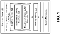
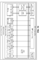
- FIG. 1 is a block diagram illustrating one configuration of an electronic device 102 in which systems and methods for rendering multiple levels of detail may be implemented.
- the electronic device 102 include smart phones, computers (e.g., desktop computers, laptop computers, etc.), head-mounted displays (e.g., virtual reality (VR) headsets, augmented reality (AR) headsets, etc.), VR devices, AR devices, tablet devices, media players, televisions, automobiles, vehicles, cameras, video camcorders, digital cameras, cellular phones, personal cameras, action cameras, aircraft, drones, unmanned aerial vehicles (UAVs), healthcare equipment, gaming consoles, personal digital assistants (PDAs), set-top boxes, media players, etc.
- the electronic device 102 may include one or more components or elements. One or more of the components or elements may be implemented in hardware (e.g., circuitry), firmware and/or a combination of hardware and software (e.g., a processor with instructions).
- the electronic device 102 may include a very long instruction word (VLIW) circuit 104 and system memory 114.
- the VLIW circuit 104 may be a circuit (e.g., processor) that implements instruction level parallelism. For example, the VLIW circuit 104 may execute instructions in parallel (e.g., concurrently).
- the VLIW circuit 104 may be coupled to (e.g., in electronic communication with) the system memory 114.
- the VLIW circuit 104 may be a device for rendering images.
- the VLIW circuit 104 may convert geometry data (e.g., geometrical model(s), two-dimensional (2D) or three dimensional (3D) geometry data, vertices, polygons, etc.) into one or more images.
- the resulting image(s) may be presented on one or more displays.
- the image(s) may be a single image to produce a 2D view or may be multiple images (e.g., stereoscopic images) to produce a 3D view.
- the VLIW circuit 104 may produce multiple images (e.g., different views) for a stereoscopic view (e.g., one image for a left eye and another image for a right eye). It should be noted that the VLIW circuit 104 may render a series of images (e.g., video).
- the VLIW circuit 104 may be implemented in hardware or in a combination of hardware and software.
- One example of the VLIW circuit 104 is a graphics processing unit (GPU).
- the electronic device 102 may perform one or more of the functions, procedures, methods, steps, etc., described in connection with one or more of Figures 2-5 , 9 , 11 , 13 and 15-24 . Additionally or alternatively, the electronic device 102 may include one or more of the structures described in connection with one or more of Figures 2-5 , 9 , 11 , 13 and 15-24 .
- the system memory 114 may store instructions and/or data. Examples of system memory 114 include random access memory (RAM), dynamic random access memory (DRAM), synchronous dynamic random access memory (SDRAM), double data rate synchronous dynamic random access memory (DDR SDRAM), DDR2, DDR3, DDR4, static random access memory (SRAM), registers, read-only memory (ROM), erasable programmable read-only memory (EPROM), electrically erasable programmable read-only memory (EEPROM), NAND flash memory, NOR flash memory, etc.
- the VLIW circuit 104 may access (e.g., read from and/or write to) the system memory 114.
- the system memory 114 may be accessible by other elements (if any) of the electronic device 102, such as one or more processors (e.g., central processing units (CPUs)).
- the system memory 114 may be separate from the VLIW circuit 104.
- Examples of instructions and/or data that may be stored by the system memory 114 may include instructions, command data, geometry data (e.g., vertices, polygons, normals (e.g., object orientations), primitives, metadata, etc.), texture data, unordered access view data, rendering parameter(s) (e.g., level of detail parameter(s)), etc.
- the electronic device 102 e.g., the system memory 114) may include one or more frame buffers.
- the frame buffer(s) may buffer (e.g., store) image data.
- the buffered image data may be presented on one or more displays.
- the VLIW circuit 104 may include one or more elements for rendering images.
- the elements may include a front end (FE), vertex processor (VPs, vertex fetcher (VF), vertex shader (VS), tessellation control shader (TCS), hull shader (HS), tessellator (e.g., tessellation engine) (TESS), tessellation evaluation shader (TES), domain shader (DS), geometry shader (GS), rasterizer (Rast), fragment shader (FS), pixel shader (PS), tiler, render output unit (ROP), clipper (Clip) and/or stream out (SOL), etc.
- a graphics pipeline 106 may be referred to as a graphics pipeline 106.
- the tessellator may be fixed function tessellation engine in some configurations.
- the tessellator (and/or one or more other elements of a graphics pipeline) may be implemented in hardware, software or a combination of hardware and software.
- the VLIW circuit 104 may include on-chip memory 110.
- the on-chip memory 110 may be implemented on the VLIW circuit 104 to provide fast memory access.
- the on-chip memory 110 may be accessed more quickly than the system memory 114.
- Examples of on-chip memory 110 may include random access memory (RAM), dynamic random access memory (DRAM), synchronous dynamic random access memory (SDRAM), double data rate synchronous dynamic random access memory (DDR SDRAM), DDR2, DDR3, DDR4, static random access memory (SRAM), registers, read-only memory (ROM), erasable programmable read-only memory (EPROM), electrically erasable programmable read-only memory (EEPROM), NAND flash memory, NOR flash memory, etc.
- RAM random access memory
- DRAM dynamic random access memory
- SDRAM synchronous dynamic random access memory
- DDR SDRAM double data rate synchronous dynamic random access memory
- SRAM static random access memory
- registers read-only memory
- ROM read-only memory
- EPROM erasable
- the on-chip memory 110 may be implemented in multiple levels (e.g., level 1 (LI), cache, level 2 (L2) cache, level 3 (L3) cache, etc.). Examples of data that may be stored by the on-chip memory 110 may include geometry data (e.g., vertices, polygons, normals, primitives, metadata, etc.), texture data, unordered access view data, one or more rendering parameters (e.g., level of detail (LOD) parameter(s)), etc.
- the on-chip memory 110 may include one or more frame buffer(s) (in addition to or alternatively from the system memory 114, for example). The frame buffer(s) may buffer (e.g., store) image data. The buffered image data may be presented on one or more displays.
- the VLIW circuit 104 may include an asynchronous memory controller 108.
- the asynchronous memory controller 108 may be implemented in hardware or a combination of hardware and software.
- the asynchronous memory controller 108 may be implemented in the VLIW circuit 104, separately from the VLIW circuit, or may be implemented partially in the VLIW circuit 104 and partially separate from the VLIW circuit 104.
- the asynchronous memory controller 108 may be configured to access memory (e.g., on-chip memory 110 and/or system memory 114) asynchronously.
- the asynchronous memory controller 108 operates "asynchronously" in the sense that the asynchronous memory controller 108 may access memory (e.g., parameter(s), level of detail (LOD) parameter(s), etc.) out of synchronization with a set of data that is being processed (e.g., tessellated).
- the VLIW circuit 104 may periodically process sets of data. Processing (e.g., tessellating) a single set of data may be referred to as a draw call.
- a draw call may be an instruction (e.g., a programmatic request, instruction, etc.) for the VLIW circuit 104 to process (e.g., render) a set of data.
- One or more parameters may be associated with and/or set for the draw call. Accordingly, a draw call may establish a LOD to be rendered for the set of data, for example.
- each set of data (e.g., draw call) has a fixed level of detail (LOD).
- LOD level of detail
- the LOD for a set of data cannot change once processing has begun on that set of data (e.g., cannot change during a draw call).
- each set of data may only have a single LOD in known approaches.
- the asynchronous memory controller 108 may asynchronously access memory (e.g., on-chip memory 110 and/or system memory 114) to enable rendering different levels of detail (e.g., different zones with different levels of detail) within a single data set (e.g., during processing of a draw call).
- the asynchronous memory controller 108 may access memory (e.g., parameter(s), LOD parameter(s), etc.) after processing (e.g., tessellation, shading, etc.) on a set of data has begun and before processing on the set of the data is completed. This may allow the VLIW circuit 104 to change LOD during processing of a set of data to produce different LODs in one set of data.
- Each set of data may include multiple primitives (e.g., points, polygons, etc.).
- each set of data may (initially) have a single LOD assigned.
- the asynchronous memory controller 108 may assign a different LOD to a set of data during processing of that data set.
- the asynchronous memory controller 108 may change the LOD for a set of data (after processing (e.g., tessellation, shading, etc.) on that set of data has begun but before processing (e.g., tessellation, shading, etc.) on that set of data has completed).
- the systems and methods disclosed herein may allow changing LOD on a per-pixel and/or per-primitive basis (even within a set of data, for instance).
- the parameters e.g., parameter(s), LOD parameter(s), etc.
- a processor e.g., central processing unit (CPU), digital signal processor (DSP), etc.
- any dedicated hardware block e.g., any hardware that deals with sensor data (e.g., eye tracking sensor data, motion sensor data, etc.)
- sensor data e.g., eye tracking sensor data, motion sensor data, etc.
- the VLIW circuit 104 may read (e.g., may always read, continuously read, periodically read, etc.) from a section of memory (e.g., on-chip memory 110 and/or system memory 114) that includes the parameters. Accordingly, the VLIW circuit 104 (e.g., GPU) may adjust accordingly per primitive instead of for an entire draw call. In some configurations, the VLIW circuit 104 may render different levels of detail in a single draw call.
- the asynchronous memory controller 108 may enable more efficient processing when rendering multiple LODs.
- multiple overlapping layers may be rendered, where each layer has a different LOD. Then, the overlapping layers may be blended. However, this approach is inefficient because the same data is rendered multiple times.
- different LODs may be rendered in a single pass. This may avoid re-rendering the same data and/or may avoid having to blend multiple layers with different levels of detail.
- the systems and methods disclosed herein may allow asynchronously changing LOD.
- rendering one or more zones of an image may be based on eye tracking.
- the electronic device 102 may render multiple zones with different levels of detail, where a zone with a highest level of detail is rendered in an area where a user is currently looking.
- the eye tracking may detect when a user changes gaze to look at a different part of the image.
- the systems and methods disclosed herein e.g., the asynchronous memory controller 108 may immediately change the LOD rendered based on the eye tracking.
- the VLIW circuit 104 may increase the LOD in an area of the image that the user has changed gaze to view, even during the processing of a data set. This may provide a better user experience.
- the systems and methods disclosed herein e.g., the asynchronous memory controller 108) may reduce the LOD in an area of the image that the user's gaze is no longer directed to. This may reduce unnecessary processing.
- the VLIW circuit 104 may include a non-uniform frame buffer controller 112.
- the non-uniform frame buffer controller 112 (e.g., multi-resolution FBO) may be implemented in hardware or a combination of hardware and software.
- the non-uniform frame buffer controller 112 may be implemented in the VLIW circuit 104, separately from the VLIW circuit 104, or may be implemented partially in the VLIW circuit 104 and partially separate from the VLIW circuit 104.
- the non-uniform frame buffer controller 112 may be implemented as part of the graphics pipeline 106.
- the non-uniform frame buffer controller 112 may be implemented as part of the on-chip memory 110.
- the non-uniform frame buffer controller 112 may be implemented in the VLIW circuit 104 but separate from the graphics pipeline 106 and the on-chip memory 110.
- the non-uniform frame buffer controller 112 may be configured to dynamically access different subsets of one or more frame buffer(s).
- the different subsets of a frame buffer may correspond to different levels of detail, zones with different levels of detail and/or different mipmap levels.
- the non-uniform frame buffer controller 112 may be configured to operate on different subsets of a frame buffer dynamically. It should be noted that there may be two or more frame buffer subsets.
- different subsets of the non-uniform frame buffer may correspond to different views (e.g., a left eye view and a right eye view for stereoscopic rendering).
- the non-uniform frame buffer may improve bandwidth utilization.
- the left eye view and right eye view may be processed concurrently (e.g., simultaneously) and saved out to system memory 114 in one pass. Additionally or alternatively, for example, the non-uniform frame buffer may enable and/or improve memory utilization for rendering multiple LODs in one pass.
- dynamically accessing different subsets of the frame buffer may include accessing at least one pixel of a first zone at a different rate from at least one pixel of a second zone.
- the first zone and the second zone may correspond to different levels of detail.
- the non-uniform frame buffer controller 112 may enable pixels of one zone (with a higher LOD, for instance) to be processed at a higher rate than pixels of another zone (with a lower LOD, for instance). This approach may allow for power savings by slowing processing of one or more zones (e.g., lower-LOD zones). It should be noted that there may be pixels from two or more zones that may be accessed at two or more different rates.
- dynamically accessing different subsets of the frame buffer may include enabling shader sub-routine swapping.
- shader sub-routine swapping may be performed when processing of a first pixel is ongoing and process of a second pixel is completed.
- a first subset of the frame buffer may be allocated for one or more pixels processed with a first shader sub-routine
- a second subset of the frame buffer may be allocated for one or more pixels processed with a second shader sub-routine.
- the electronic device 102 may swap shader sub-routines to occupy the second subset of the frame buffer. This may provide more efficient processing by allowing frame buffer capacity to be utilized more efficiently.
- two or more subsets of the frame buffer may be utilized to enable sub-routine swapping for one or more of the subsets.
- the non-uniform frame buffer controller 112 may be configured to substitute a processed first sample of a first pixel for a second sample of a second pixel to avoid processing the second sample of the second pixel.
- the first pixel may have a different number of samples than the second pixel. For example, a first pixel from a first zone may have a higher LOD than a neighboring second pixel from a second zone with a lower LOD.
- the non-uniform frame buffer controller 112 may replace the (unprocessed) sample of the second pixel with the (processed) sample of the first pixel. In this way, the non-uniform frame buffer controller 112 may reduce processing. It should be noted that the non-uniform frame buffer controller 112 may replace one or more (unprocessed) samples of one or more pixels with one or more (processed) samples of one or more other pixels.
- the electronic device 102 may include and/or may be coupled to one or more displays (e.g., head-mounted displays).
- the display(s) may be configured to present the different levels of detail.
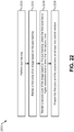
- Figure 2 is a flow diagram illustrating one configuration of a method 200 for rendering multiple levels of detail. The method 200 may be performed by the electronic device 102 described in connection with Figure 1 .
- the electronic device 102 may obtain 202 geometry data.
- the electronic device 102 may load geometry data from storage (e.g., hard disk storage, removable storage such as an external hard drive, digital video disc (DVD) drive, Blu-Ray drive, compact disc (CD), thumb drive, etc.) into memory (e.g., system memory 114 and/or on-chip memory 110).
- the electronic device 102 may receive geometry data from another device.
- the electronic device 102 may receive geometry data via a communication interface (e.g., Ethernet, Institute of Electrical and Electronics Engineers (IEEE) 802.11 interface, cellular network interface, etc.) and load the geometry data into memory (e.g., system memory 114 and/or on-chip memory 110).
- a communication interface e.g., Ethernet, Institute of Electrical and Electronics Engineers (IEEE) 802.11 interface, cellular network interface, etc.
- Examples of geometry data may include points, lines and/or polygons (e.g., triangles), etc.
- the electronic device 102 may render 204 different levels of detail asynchronously. This may be accomplished as described above in connection with Figure 1 .
- the electronic device 102 may asynchronously access the memory (e.g., system memory 114 and/or on-chip memory 110) to render different levels of detail.
- the electronic device 102 may change a LOD for a set of data during processing (where the set of data initially had a different LOD, for example).
- rendering 204 different levels of detail asynchronously may include performing dynamic LOD tessellation.
- the electronic device 102 may dynamically access 206 different subsets of a frame buffer. This may be accomplished as described above in connection with Figure 1 .
- the electronic device 102 may access at least one pixel of a first zone at a different rate from at least one pixel of a second zone.
- the electronic device 102 may enable shader sub-routine swapping when processing of a first pixel is ongoing and process of a second pixel is completed.
- the electronic device 102 may substitute a processed first sample of a first pixel for a second sample of a second pixel to avoid processing the second sample of the second pixel.
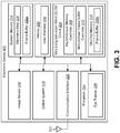
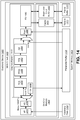
- Figure 3 is a block diagram illustrating one configuration of an electronic device 302 in which systems and methods for rendering multiple levels of detail may be implemented.
- the electronic device 302 described in connection with Figure 3 may be an example of the electronic device 102 described in connection with Figure 1 .
- one or more of the components or elements of the electronic device 302 may be similar to corresponding components or elements described in connection with Figure 1 .
- One or more of the components or elements may be implemented in hardware (e.g., circuitry) or a combination of hardware and software (e.g., a processor with instructions).
- the electronic device 302 may include a very long instruction word (VLIW) circuit 304, system memory 314, one or more displays 332, one or more image sensors 316, one or more optical systems 318, one or more communication interfaces 320, one or more antennas 322 and/or one or more processors 324.
- VLIW very long instruction word
- the VLIW circuit 304 may be coupled to (e.g., in electronic communication with) the system memory 314.
- the VLIW circuit 304 may be a device for rendering images as described above in connection with one or more of Figures 1 and 2 .
- the resulting image(s) may be presented on the one or more displays 332.
- the VLIW circuit 304 may be separate from the processor 324 in some implementations. In other implementations, the VLIW circuit 304 may be integrated into the processor 324.
- the communication interface 320 may enable the electronic device 302 to communicate with one or more other electronic devices.
- the communication interface 320 may provide an interface for wired and/or wireless communications.
- the communication interface 320 may be coupled to one or more antennas 322 for transmitting and/or receiving radio frequency (RF) signals.
- RF radio frequency
- the communication interface 320 may enable one or more kinds of wireline (e.g., Universal Serial Bus (USB), Ethernet, Video Graphics Array (VGA), Digital Visual Interface (DVI), High Definition Multimedia Interface (HDMI), DisplayPort, Mobile High-Definition Link (MHL), etc.) communication.
- USB Universal Serial Bus
- VGA Video Graphics Array
- DVI Digital Visual Interface
- HDMI High Definition Multimedia Interface
- MHL Mobile High-Definition Link
- multiple communication interfaces 320 may be implemented and/or utilized.
- one communication interface 320 may be a cellular (e.g., 3G, Long Term Evolution (LTE), CDMA, etc.) communication interface 320
- another communication interface 320 may be an Ethernet interface
- another communication interface 320 may be a universal serial bus (USB) interface
- yet another communication interface 320 may be a wireless local area network (WLAN) interface (e.g., Institute of Electrical and Electronics Engineers (IEEE) 802.11 interface)
- yet another communication interface 320 may be a Bluetooth interface.
- WLAN wireless local area network
- IEEE Institute of Electrical and Electronics Engineers 802.11 interface
- the electronic device 302 may perform one or more of the functions, procedures, methods, steps, etc., described in connection with one or more of Figures 1 , 3-5 , 9 , 11 , 13 and 15-24 . Additionally or alternatively, the electronic device 302 may include one or more of the structures described in connection with one or more of Figures 1 , 3-5 , 9 , 11 , 13 and 15-24 .
- the system memory 314 may store instructions and/or data.
- the system memory 314 described in connection with Figure 3 may be an example of the system memory 114 described in connection with Figure 1 .
- the VLIW circuit 304 may access (e.g., read from and/or write to) the system memory 314.
- the system memory 314 may also be accessible by the processor(s) 324.
- the system memory 314 may store geometry data 328.
- the system memory 314 may include a frame buffer 330a.
- the frame buffer 330a may be a portion of the system memory 314 for storing image data.
- the buffered image data may be presented on the one or more displays 332 in some configurations.
- the VLIW circuit 304 may include one or more elements for rendering images.
- the elements may include a front end (FE), vertex processor (VPs, vertex fetcher (VF), vertex shader (VS), tessellation control shader (TCS), hull shader (HS), tessellator (e.g., tessellation engine) (TESS), tessellation evaluation shader (TES), domain shader (DS), geometry shader (GS), rasterizer (Rast), fragment shader (FS), pixel shader (PS), tiler, render output unit (ROP), clipper (Clip) and/or stream out (SOL), etc.
- FE front end
- VPs vertex processor
- VF vertex fetcher
- VS vertex shader
- TCS tessellation control shader
- HS hull shader
- tessellator e.g., tessellation engine
- TES tessellation evaluation shader
- DS domain shader
- GS geometry shader
- the VLIW circuit 304 may include on-chip memory 310.
- the on-chip memory 310 described in connection with Figure 3 may be an example of the on-chip memory 110 described in connection with Figure 1 .
- the on-chip memory 310 may include a frame buffer 330b (in addition to or alternatively from the frame buffer 330a in system memory 314, for example).
- the frame buffer may be a portion of the on-chip memory 310 for storing image data.
- the buffered image data may be presented on the one or more displays 332 in some configurations.
- the VLIW circuit 304 may include an asynchronous memory controller 308.
- the asynchronous memory controller 308 may be implemented in hardware or a combination of hardware and software.
- the asynchronous memory controller 308 may be implemented in the VLIW circuit 304, separately from the VLIW circuit, or may be implemented partially in the VLIW circuit 304 and partially separate from the VLIW circuit 304.
- the asynchronous memory controller 308 may be configured to access memory (e.g., on-chip memory 310 and/or system memory 314) asynchronously. It should be noted that the asynchronous memory controller 308 may utilize (e.g., access) the on-chip memory 110 and/or the system memory 114 (e.g., either or both).
- the asynchronous memory controller 308 described in connection with Figure 3 may be an example of the asynchronous memory controller 108 described in connection with Figure 1 .
- the asynchronous memory controller 308 described in connection with Figure 3 may operate as described in connection with the asynchronous memory controller 108 described in connection with Figure 1 .
- the VLIW circuit 304 may include a non-uniform frame buffer controller 312.
- the non-uniform frame buffer controller 312 may be implemented in hardware or a combination of hardware and software.
- the non-uniform frame buffer controller 312 may be implemented in the VLIW circuit 304, separately from the VLIW circuit 304, or may be implemented partially in the VLIW circuit 304 and partially separate from the VLIW circuit 304.
- the non-uniform frame buffer controller 312 may be implemented as part of the graphics pipeline.
- the non-uniform frame buffer controller 312 may be implemented as part of the on-chip memory 310.
- the non-uniform frame buffer controller 312 may be implemented in the VLIW circuit 304 but separate from the graphics pipeline 306 and the on-chip memory 310.
- the non-uniform frame buffer controller 312 described in connection with Figure 3 may be an example of the non-uniform frame buffer controller 112 described in connection with Figure 1 .
- the non-uniform frame buffer controller 312 described in connection with Figure 3 may operate as described in connection with the non-uniform frame buffer controller 112 described in connection with Figure 1 .
- the electronic device 302 may perform single-pass multi-LOD rendering.
- Multi-LOD rendering may include rendering different zones of an image with different levels of detail.
- Single-pass multi-LOD rendering may include rendering different zones with different levels of detail (e.g., tessellated levels of detail) in a single pass (without repeatedly processing any pixel, for example).
- Single-pass foveated rendering may be an example of single-pass multi-LOD rendering, where different zones with different levels of detail may be based on eye tracking.
- a zone may be a circular area (or an area of another shape) approximately centered on the point of a display (e.g., image) where the user is looking.
- single-pass rendering may include performing one pass (e.g., processing pass) over the data and/or texture to be rendered, even though both a left-eye view and a right-eye view need to be rendered.
- one pass e.g., processing pass
- some configurations of the systems and methods disclosed herein may utilize as much of the data for both eye views as much as possible before moving the data between system memory and on-chip memory (e.g., GPU memory).
- the asynchronous memory controller 308 and/or the non-uniform frame buffer controller 312 may enable the performance of single-pass multi-LOD rendering (e.g., single-pass foveated rendering).
- the asynchronous memory controller 308 may allow reading parameter(s) (e.g., level of detail (LOD) parameter(s)) from a volatile memory block (e.g., dynamically adapting during a draw call).
- the asynchronous memory controller 308 may allow one or more of a tessellation control shader (TCS), tessellator (TESS), tessellation evaluation shader (TES), geometry shader (GS), rasterizer and fragment shader (FS) to access one or more parameters from a volatile memory block (e.g., to dynamically adapt during a draw call).
- TCS tessellation control shader
- TESS tessellator
- TES tessellation evaluation shader
- GS geometry shader
- FS fragment shader
- the VLIW circuit 304 may include a rasterizer.
- the rasterizer may enable MSAA to perform more sampling of the primitives, which in turn may activate more fragment shader (FS) evaluations. Additionally sampling of the primitives may be performed to avoid artifacts like jaggies, which are due to not enough samples being processed and averaged.
- FS fragment shader
- the electronic device 302 may obtain one or more images (e.g., digital images, image frames, video, etc.).
- the one or more images may be images of one or more users and/or a scene (e.g., one or more objects and/or background).
- the electronic device 302 may include one or more image sensors 316 and/or one or more optical systems 318 (e.g., lenses) that focus images of objects that are located within the field of view of the optical system(s) 318 onto the image sensor(s) 316.
- the image sensor(s) 316 may capture the one or more images.
- the image sensor(s) 316 and/or optical system(s) 318 may be coupled to and/or controlled by the processor 324.
- the electronic device 302 may request and/or receive the one or more images from another device (e.g., an external image sensor coupled to the electronic device 302, a network server, traffic camera, drop camera, automobile camera, web camera, etc.). In some configurations, the electronic device 302 may request and/or receive the one or more images via the communication interface 320.
- the electronic device 302 may or may not include a camera (e.g., an image sensor 316 and/or optical system 318) and may receive images from a remote device.
- the one or more image sensors 316 included in the electronic device 302 and/or one or more other image sensors coupled to the electronic device 302 may be oriented to capture one or more images of a user.
- a smartphone may include a camera mounted on the same face as a display (e.g., display 332). In this way, the camera may capture images of a user while the user is looking at the display.
- a camera may be mounted in a console and/or steering wheel of a vehicle to capture images of a user (e.g., driver).
- the one or more image sensors 316 included in the electronic device 302 and/or one or more other image sensors coupled to the electronic device 302 may be oriented to capture scenery.
- one or more cameras may be mounted on the back side of a smart phone.
- one or more cameras may be mounted on the exterior of a vehicle.
- the electronic device 302 may utilize the images of scenery in augmented reality (AR) applications, virtual reality (VR) applications and/or other applications (e.g., surround view visualization, driver assistance, advanced driver assistance systems (ADAS), etc.).
- AR augmented reality
- VR virtual reality
- ADAS advanced driver assistance systems
- the image(s) captured by the image sensor(s) 316 and/or received via the communication interface(s) 320 may be utilized by the electronic device 302 for eye tracking.
- the processor 324 may include and/or implement an eye tracker 326.
- the eye tracker 326 may track the gaze (e.g., look direction) of one or more users' eye(s).
- the eye tracker 326 may locate the eye(s) of one or more users in the image(s) and may estimate the gaze (e.g., look direction) of the user(s).
- the eye tracker 326 may determine (e.g., estimate) where a user is looking on a display (e.g., display 332 or an external display) and/or where a user is looking on an image presented by a display. In other words, the eye tracker 326 may determine (e.g., estimate) where a user's gaze is directed relative to an image and/or a display.
- a display e.g., display 332 or an external display
- the eye tracker 326 may determine (e.g., estimate) where a user's gaze is directed relative to an image and/or a display.
- rendering one or more zones of an image may be based on eye tracking.
- the zones of the image may have different levels of detail.
- the electronic device 302 may render multiple zones with different levels of detail, where a zone with a highest level of detail is rendered in an area where a user is currently looking. In some configurations, this may be referred to as foveated rendering.
- the eye tracker 326 may produce eye tracking information.
- the eye tracking information may indicate where a user's gaze is directed (e.g., users' gazes are directed) relative to a display and/or image.
- the processor 324 and/or the VLIW circuit 304 may determine one or more LOD parameters based on the eye tracking information.
- the LOD parameter(s) may indicate a LOD to be rendered for one or more zones of an image.
- the LOD parameter(s) may be stored in system memory 314 and/or on-chip memory 310.
- the LOD parameter(s) may be updated asynchronously in relation to a set of data (e.g., draw call) that is being processed by the VLIW circuit 304.
- the asynchronous memory controller 308 may read the LOD parameter(s) (from the system memory 314 and/or on-chip memory 310) during the processing of the data set (e.g., draw call). For example, the asynchronous memory controller 308 may update tessellation settings during the processing of the data set (e.g., draw call).
- the eye tracker 326 may detect when a user changes gaze to look at a different part of the image.
- the systems and methods disclosed herein e.g., the asynchronous memory controller 308 may immediately change the LOD rendered based on the eye tracking (e.g., the eye tracking information and/or LOD parameter(s)).
- the asynchronous memory controller 308 may read one or more parameters (e.g., LOD parameters), which may change during the processing of a data set (e.g., draw call).
- the VLIW circuit 304 may increase the LOD in an area (e.g., zone) of the image that the user has changed gaze to view, even during the processing of a data set.
- a zone may be a circular area (or an area of another shape) approximately centered on the point of a display (e.g., image) where the user is looking.
- a zone may be the entire area of an image corresponding to a window that the user is viewing.
- the electronic device 302 may include a camera application and/or a display 332.
- the camera application When the camera application is running, images of objects that are located within the field of view of the optical system 318 may be captured by the image sensor 316. The images that are being captured by the image sensor 316 may be presented on the display 332. In some configurations, these images may be displayed in rapid succession at a relatively high frame rate so that, at any given moment in time, the objects that are located within the field of view of the optical system 318 are presented on the display 332.
- one or more of the elements illustrated in the electronic device 302 may be optional.
- one or more of the elements illustrated in the electronic device 302 may or may not be included and/or implemented.
- one or more of the elements illustrated in the processor 324 and/or VLIW circuit 304 may be implemented separately from the processor 324 and/or VLIW circuit 304 (e.g., in other circuitry, on another processor, on a separate electronic device, etc.).
- the image sensor 316, the optical system 318, the communication interface 320, the processor 324, the eye tracker 326 and/or the display 332 may not be implemented on the electronic device 302.
- the electronic device 302 may receive images and/or eye tracking information from another device. Additionally or alternatively, one or more displays may be implemented on one or more separate devices.
- the electronic device 302 may present a user interface 334 on the display 332.
- the user interface 334 may enable a user to interact with the electronic device 302.
- the display 332 may be a touchscreen that receives input from physical touch (by a finger, stylus or other tool, for example).
- the electronic device 302 may include or be coupled to another input interface.
- the electronic device 302 may include a camera facing a user and may detect user gestures (e.g., hand gestures, arm gestures, eye tracking, eyelid blink, etc.).
- the electronic device 302 may be coupled to a mouse and may detect a mouse click. It should be noted that no user input may be necessary in some configurations.
- the electronic device 302 may optionally include a motion sensor (e.g., gyroscope(s), accelerometer(s), etc.).
- the motion sensor may detect motion and/or an orientation (of the electronic device 302, for instance).
- the image being rendered may be based on motion and/or orientation information.
- the electronic device 302 may be a head-mounted display (e.g., a virtual reality (VR) headset, augmented reality (AR) headset, etc.), a vehicle (e.g., automobile, drone, airplane, etc.), a mobile device (e.g., smartphone) or other device that may utilize motion and/or orientation information to render an image.
- VR virtual reality
- AR augmented reality
- the motion and/or orientation information may indicate a general viewing direction in a rendered scene.
- the electronic device 302 may render the image based on this viewing direction in addition to or alternatively from the eye tracking information in some configurations.
- the use of a motion sensor may illustrate another aspect of the asynchronous operation of the asynchronous memory controller 308.
- a motion sensor may provide motion information and/or orientation information to memory (e.g., system memory 314 and/or on-chip memory 310) at a particular rate (e.g., 1000 hertz (Hz)), while the VLIW circuit 304 may render frames at a comparatively lower rate (e.g., 30 frames per second (fps)).
- the asynchronous memory controller 308 may asynchronously change one or more rendering operations (e.g., tessellation) in the midst of rendering a set of data based on the motion information and/or orientation information.
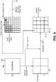
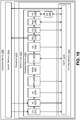
- Figure 4 is a diagram illustrating one example of a non-uniform frame buffer 430.
- the frame buffer 430 has a capacity of 2n x 2m pixels.
- the electronic device 302 may optionally tile 432 the frame buffer 430 into tiles 436. In the example illustrated in Figure 4 , four tiles 436 of size (n, m) are illustrated.
- on-chip memory 310 or a portion of on-chip memory 310 may be limited to the size of a tile 436. Accordingly, the electronic device 302 may split the frame buffer 430 into tiles 436. In other implementations, the on-chip memory 310 or a portion of on-chip memory 310 may be large enough to accommodate the entire frame buffer 430 and no tiling 434 may be performed.
- the electronic device 302 may subdivide 438 the frame buffer 430 and/or tiles 436 into scaled portions 440.
- the frame buffer 430 and/or tiles 436 may be subdivided to fit multiple resolutions and/or levels of detail.
- the scaled portions 440 are of size (n/c, m/c), where c is a scaling factor.
- the scaling factor c may vary and/or may be selected based on the configuration.
- the electronic device 302 may dynamically access different subsets 442a-c of the frame buffer 430.
- the electronic device 302 may dynamically access buffer subset A 442a, buffer subset B 442b and buffer subset C 442c. It should be noted that fewer or more buffer subsets may be utilized. It should also be noted that all or only a portion of the frame buffer 430 may be occupied by buffer subsets. For example, the other non-hatched portions of the frame buffer may be utilized by one or more other subsets.
- Dynamic access (e.g., reading and/or writing) of different frame buffer subsets may enable one or more approaches to provide greater control and/or efficiency in rendering images.
- dynamic access of different frame buffer subsets may enable single-pass multi-LOD rendering. This is because rendering a zone at one LOD does not need to be completed before rendering another zone at a different LOD can be started.
- one or more of the buffer subsets 442a-c may correspond to different image zones.
- buffer subset A 442a may correspond to a zone with a highest LOD
- buffer subset B 442b may correspond to a zone with a medium LOD
- buffer subset C 442c may correspond to a zone with a lower LOD.
- the VLIW circuit 304 may render a highest LOD zone, which may be written to buffer subset A 442a while concurrently or sequentially rendering a medium LOD zone, which may be written to buffer subset B 442b.
- different LOD zones may be rendered in any order (e.g., from highest LOD to lowest, in reverse order or another order).
- dynamic access of different frame buffer subsets may allow processing different zones at different rates (e.g., a larger frame buffer subset may be allocated for one zone to be processed more quickly, while a smaller frame buffer subset may be allocated for another zone to be processed more slowly).
- dynamic access of different frame buffer subsets may enable parallel shader processes (e.g., sub-routines). For instance, different shader processes may be executed in parallel, where one shader process accesses one subset of the frame buffer and another shader process accesses another subset of the frame buffer. Additionally or alternatively, dynamic access of different frame buffer subsets may allow shader sub-routine swapping. For example, a first shader sub-routine may be executed that accesses buffer subset A 442a. While the first shader sub-routine is ongoing, a second shader sub-routine that accesses buffer subset B 442b may finish.
- shader processes e.g., sub-routines
- the second shader sub-routine may be swapped for another shader sub-routine (which may access buffer subset B 442b, for example) while the first shader sub-routine is ongoing. This may allow greater efficiency in utilizing the space of the frame buffer, rather than having to wait for a shader sub-routine to finish before another can be started.
- dynamic access of different frame buffer subsets may enable sample substitution.
- the non-uniform frame buffer controller 312 may swap one or more samples of a processed pixel for one or more samples of another pixel.
- the VLIW circuit 304 may perform anti-aliasing (e.g., multi-sample anti-aliasing (MSAA)). In performing anti-aliasing, different pixels may have different numbers of samples.
- MSAA multi-sample anti-aliasing
- a first (e.g., "fine") pixel in buffer subset A 442a may have 4 samples and may use higher quality shading
- a nearby (e.g., neighboring) second (e.g., "coarse”) pixel in buffer subset B 442b may have 1 sample and use lower quality shading.
- the non-uniform frame buffer controller 312 may substitute a sample of the first pixel for a sample of the second pixel. This may avoid performing any of the processing for the second pixel. Additionally or alternatively, the non-uniform frame buffer controller 312 may perform sample substitution in processing mipmaps.
- the non-uniform frame buffer controller 312 may substitute a sample from a higher level (in buffer subset A 442a, for instance) for a sample from a lower level (in buffer subset B 442b, for instance). This may avoid some or processing at one or more lower levels.
- the non-uniform frame buffer controller 312 may enable dynamic dispatch of shader processing (e.g., sub-routines, kernels, etc.), may enable pixel sample substitution and/or may provide a multi-LOD frame buffer.
- shader processing e.g., sub-routines, kernels, etc.
- the frame buffer 430 may store image data that may be streamed out as multiple rendered targets 444.
- Listing (1) illustrates one example of pseudocode that illustrates one approach for non-uniform frame buffer functionality. It should be noted that GLSL is an abbreviation for OpenGL Shading Language and SSBO is an abbreviation for Shader Storage Buffer Object. Listing (1) illustrates how multiple zones with different levels of detail
- Figure 5 is a flow diagram illustrating a more specific configuration of a method 500 for rendering multiple levels of detail.
- the method 500 may be performed by the electronic device 302 described in connection with Figure 3 .
- the electronic device 302 may obtain 502 geometry data (e.g., geometry data 328). This may be accomplished as described in connection with one or more of Figures 1-3 .
- the electronic device 302 may load geometry data from storage into memory (e.g., system memory 314 and/or on-chip memory 310) and/or may receive geometry data from another device and load the geometry data into memory (e.g., system memory 314 and/or on-chip memory 310).
- the electronic device 302 may perform 504 eye tracking. This may be accomplished as described in connection with Figure 3 .
- the electronic device 302 may obtain (e.g., capture and/or receive) one or more images and may determine where a user's gaze is directed (e.g., where a user is looking on a display and/or an image being presented on the display) based on the one or more images.
- the electronic device 302 may render 506 different levels of detail asynchronously based on the eye tracking. This may be accomplished as described above in connection with one or more of Figures 1-3 .
- the electronic device 302 may asynchronously access the memory (e.g., system memory 314 and/or on-chip memory 310) to render different levels of detail based on the eye tracking.
- the electronic device 302 may change a LOD for a set of data during processing (where the set of data initially had a different LOD, for example) when the zone for the set of data changes based on the eye tracking.
- the electronic device 302 may increase the LOD for the set of data when a user's gaze is directed to an area of the image corresponding to the set of data.
- the electronic device 302 may decrease the LOD for the set of data when a user's gaze direction moves away from an area of the image corresponding to the set of data.
- rendering 506 different levels of detail asynchronously may include performing dynamic LOD tessellation.
- the memory e.g., system memory 314 and/or on-chip memory 310
- LOD tessellation parameter(s) e.g., a degree of tessellation
- the asynchronous memory controller 308 may access the updated LOD tessellation parameter to change the LOD tessellation asynchronously.
- the electronic device 302 may dynamically access 508 different subsets of a frame buffer. This may be accomplished as described above in connection with one or more of Figures 1-4 .
- the electronic device 302 may access at least one pixel of a first zone at a different rate from at least one pixel of a second zone.
- the electronic device 302 may enable shader sub-routine swapping when processing of a first pixel is ongoing and process of a second pixel is completed.
- the electronic device 302 may substitute a processed first sample of a first pixel for a second sample of a second pixel to avoid processing the second sample of the second pixel.
- the electronic device 302 may present 510 the rendered image.
- the electronic device 302 may stream out image data that has been rendered 506 with different levels of detail asynchronously.
- the image data may be provided to an integrated display 332.
- the image data may be provided to a remote display that is in communication with the electronic device 302.
- the electronic device 302 may provide the image data to a display that is coupled to the electronic device 302 (via VGA, DVI, HDMI, etc.)
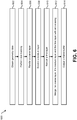
- Figure 6 is a flow diagram illustrating example of a method 600 for foveated rendering.
- geometry data is obtained 602.
- Eye tracking is also performed 604.
- a coarse layer is rendered 606, a medium layer is rendered 608 and a fine layer is rendered 610.
- the fine layer may be rendered 610 on an image where a user's gaze is directed.
- the medium layer may be rendered 608 in a larger area that overlaps the fine layer area.
- the coarse layer may be rendered 606 in an even larger area (e.g., the whole image) that includes the medium layer area and the fine layer area. Accordingly, there may be significant overlap between the layers.
- the coarse layer, the medium layer and the fine layer may be merged 612 with anti-aliasing.
- the resulting image may be output 614 to the frame buffer.
- the method 600 may include rendering significant amounts of overlapping areas.
- the fine detail area may be rendered three times: once at the coarse layer, once at the medium layer, and once at the fine layer. This may be inefficient as it performs multiple rendering passes over the same pixels.
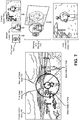
- Figure 7 illustrates one example of foveated rendering.
- Figure 7 illustrates an example of a scene for foveated rendering.
- the scene for foveated rendering includes a coarse detail area 748, a medium detail area 750 and a fine detail area 752.
- one approach to foveated rendering includes rendering the coarse layer 754, rendering the medium layer 756 and rendering the fine layer 758.
- merging and blending 760 may be performed on the coarse layer 754, medium layer 756 and fine layer 758 to produce a final blended image 762.
- blend mask A 764a between the medium layer 756 and coarse layer 754 may be used to blend the medium layer 756 and coarse layer 754.
- blend mask B 764b between the medium layer 756 and fine layer 758 may be used to blend the medium layer 756 and fine layer 758.
- this approach renders the same pixels in multiple passes, leading to inefficiencies.
- one or more of the blend masks 764a-b may provide a weighted (e.g., gradual) blend in some configurations, where the blending weight increases from the outer edges of the blend masks to the inner area.
- the coarse layer 754 and/or the final blended image 762 are illustrated in Figure 7 as subsets of the entire scene for convenience. However, the coarse layer 754 and/or the final blended image 762 may cover the entire scene.
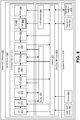
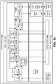
- Figure 8 is a block diagram illustrating an example of an electronic device 866 including a very long instruction word (VLIW) circuit 868.
- Figure 8 illustrates one example of an architecture for graphics processing.
- This architecture may provide immediate mode rendering (IMR) with a high-bandwidth design at the cost of power and die area.
- IMR immediate mode rendering
- cache 801 may be utilized to reduce bandwidth (e.g., to avoid repeated sampling, reading from and/or writing to system memory 805).
- the cache 801 may be large enough to accommodate data for an entire image frame.
- one or more of the graphics pipelines described herein may have one or more aspects similar to DirectX and/or OpenGL pipelines and/or application programming interfaces (APIs).
- APIs application programming interfaces
- the electronic device 866 may include a VLIW circuit 868 (e.g., GPU) and system memory 805 (e.g., DRAM).
- the VLIW circuit 868 may include a graphics pipeline 870 and on-chip memory 803.
- the graphics pipeline 870 may include one or more of a front-end (FE) 872, a vertex fetcher (VF) 874, vertex shader (VS) 876, tessellation control shader (TCS) 878, tessellator (TESS) 880 (e.g., tessellation engine), tessellation evaluation shader (TES) 882, geometry shader (GS) 884, rasterizer (Rast) 886, fragment shader (FS) 890 and render output unit (ROP) 894.
- FE front-end
- VF vertex fetcher
- VS vertex shader
- TCS tessellation control shader
- TCS tessellator
- TES tessellator
- TES tessel
- the on-chip memory 803 may include a buffer 896, composition/decomposition (C/D) memory 898 and cache 801.
- the buffer 896 may be and/or include a texture buffer, frame buffer and/or another block of on-chip memory 910.
- the system memory 805 may include command data (Cmd) 807, vertex data 809, texture data and unordered access view data 811 and rendered targets data 813.
- the electronic device 866 may load command data 807 and vertex data 809 from the system memory 805 to the cache 801 in on-chip memory 803.
- the vertex data 809 may indicate one or more points (e.g., vertices), lines and/or polygons.
- the vertex data 809 may represent a scene and/or one or more objects in a scene.
- the FE 872 may provide an interface between the cache 801 and the graphics pipeline 870 (e.g., VF 874). For example, the FE 872 may obtain data to be deformatted by the VF 874 and/or may control the VF 874 regarding the data (e.g., vertex data) that is retrieved from the cache 801.
- the data e.g., vertex data
- the VF 874 may fetch vertex data from the cache 801 into the graphics pipeline 870.
- the VF 874 may access the buffer 896.
- the VF may write data to the buffer 896.
- the VF 874 may provide the vertex data to the VS 876. Additionally or alternatively, the VS 876 may retrieve vertex data from the buffer 896.
- the VS 876 may transform the vertex data into a different space. For example the VS 876 may transform the vertex data from three-dimensional (3D) space into a two-dimensional (2D) space. The VS 876 may provide the transformed vertex data to the TCS 878 and/or may store transformed vertex data in the buffer 896.
- 3D three-dimensional
- 2D two-dimensional
- the TCS 878 may receive vertex data (e.g., transformed vertex data) from the VS 876 and/or from the buffer 896.
- the TCS 878 may transform the basis of the vertex data (e.g., the transformed vertex data).
- the TCS 878 may transform the basis of the vertex data to a basis for tessellation (e.g., for efficiently subdividing polygons such as triangles).
- the TCS 878 may store information in the cache 801.
- the TCS 878 may store a basis indicator that indicates the basis transformation performed by the TCS 878.
- the basis-transformed vertex data may be provided to the TESS 880.
- the TESS 880 may tessellate the vertex data (e.g., basis-transformed vertex data). For example, the TESS 880 may generate more vertices based on the vertex data (e.g., may subdivide triangles into more triangles). The TESS 880 may operate based on a LOD parameter.
- the LOD parameter may specify the LOD and/or may indicate a degree of tessellation for the TESS 880 to perform.
- the tessellated vertex data may be provided to the TES 882.
- the TES 882 may transform the basis of the vertex data (e.g., tessellated vertex data). For example, the TES 882 may transform the basis of the vertex data back to the basis before the basis transform applied by the TCS 878. In some configurations, the TES 882 may read the basis indicator from the cache 801 in order to transform (e.g., inverse transform) the basis of the vertex data. The TES 882 may provide vertex data (e.g., the inverse basis-transformed vertex data) to the GS 884 and/or store the vertex data in the buffer 896.
- vertex data e.g., tessellated vertex data
- the TES 882 may transform the basis of the vertex data back to the basis before the basis transform applied by the TCS 878.
- the TES 882 may read the basis indicator from the cache 801 in order to transform (e.g., inverse transform) the basis of the vertex data.
- the TES 882 may provide vertex data (e.
- the GS 884 may perform one or more operations on the vertex data (e.g., the inverse basis-transformed vertex data). For example, the GS 884 may generate additional geometry based on the vertex data. The GS 884 may provide the vertex data (with additional geometry, for example) to the rasterizer 886 and/or the cache 801.
- the vertex data e.g., the inverse basis-transformed vertex data
- the GS 884 may generate additional geometry based on the vertex data.
- the GS 884 may provide the vertex data (with additional geometry, for example) to the rasterizer 886 and/or the cache 801.
- the rasterizer 886 may receive the vertex data from the GS 884 and/or the cache 801. The rasterizer 886 may rasterize the vertex data. For example, the rasterizer may convert the vertex data to pixel data. The pixel data may be provided to the FS 890.
- the FS 890 may perform fragment shading or pixel shading on the pixel data. For example, the FS 890 may determine one or more attributes (e.g., color, brightness, transparency, etc.) of one or more pixels. In some configurations, the FS 890 may perform hidden surface removal (HSR).
- the FS 890 may include a composition/decomposition (C/D) block 892. Alternatively, the C/D 892 may be separate from the FS 890 and/or coupled to the FS 890.
- the C/D 892 may perform operations such as texturing and/or blending. For example, the C/D 892 may blend multiple layers to determine a final pixel value. In some configurations, the C/D 892 may combine different frame buffers (e.g., may blend multiple images together per pixel). It should be noted the C/D 892 may be implemented on-chip (on the VLIW circuit 868), in the graphics pipeline 870, in the on-chip memory 803 and/or separate from the VLIW circuit 868. The C/D 892 may not be implemented in system memory 805 in some configurations. The C/D 892 may operate on image data before the image data is written out to system memory 805 and/or to another stream out (e.g., HDMI stream out).
- another stream out e.g., HDMI stream out
- the FS 890 (and/or C/D 892) may access C/D memory 898.
- the system memory 805 may provide texture data and/or unordered access view data 811 to the cache 801.
- the FS 890 may perform one or more operations by accessing the C/D memory and/or the cache 801.
- the FS 890 may provide the pixel data (e.g., processed pixel data) to the ROP 894.
- the ROP 894 may output the pixel data (e.g., processed pixel data). For example, the ROP 894 may output the pixel data via the C/D memory 898 and/or cache 801 to system memory 805 as rendered targets data 813.
- the rendered targets data 813 may be provided (e.g., output) for presentation. For example, the rendered targets data 813 may be sent to a display for presentation.
- each data set may have one or more established parameters for rendering (e.g., rendering parameter(s)).
- each data set may have a fixed LOD assigned for tessellation operations. Accordingly, LOD may not be changed during rendering for a data set (e.g., during a draw call). This may result in multiple passes for rendering multiple LODs as described in connection with Figures 6-7 , for example.
- a frame buffer (which may be implemented in the on-chip memory 803, buffer 896 and/or cache 801) may be uniform.
- the frame buffer may include uniform data (e.g., data with the same LOD, data with the same number of pixel samples, data from the same shader sub-routine, etc.). For instance, subsets of the buffer may not be accessed independently (e.g., concurrently by different shader sub-routines).
- the frame buffer may be uniform in a sense that only one data write to the frame buffer may occur at a time. Additionally or alternatively, the frame buffer may be uniform in the sense that each data write may only be from a single shader sub-routine at a time. Additionally or alternatively, the frame buffer may be uniform in the sense that each data write may only include data with the same LOD and/or with the same number of pixel samples.
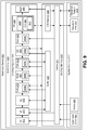
- Figure 9 is a block diagram illustrating an example of the systems and methods disclosed herein implemented in the architecture described in connection with Figure 8 .
- Figure 9 illustrates an electronic device 902.
- the electronic device 902 described in connection with Figure 9 may be an example of one or more of the electronic devices 102, 302 described above in connection with one or more of Figures 1-5 .
- the electronic device 902 may be configured to perform one or more of the methods, functions, steps, operations, etc., described in connection with one or more of Figures 1-5 .
- the electronic device 902 may include a VLIW circuit 904 (e.g., a GPU) and system memory 914.
- the VLIW circuit 904 may be one example of one or more of the VLIW circuits 104, 304 described above in connection with one or more of Figures 1-5
- the system memory 914 may be an example of one or more of the system memories 114, 314 described in connection with one or more of Figures 1-5 .
- the system memory 914 may include command data (Cmd) 907, vertex data 909, texture & unordered access view data 911 and/or rendered target data 913.
- One or more of the command data (Cmd) 907, vertex data 909, texture & unordered access view data 911 and/or rendered target data 913 may be similar to corresponding data described in connection with Figure 8 .
- the VLIW circuit 904 may include a graphics pipeline 906 and on-chip memory 910.
- the graphics pipeline 906 described in connection with Figure 9 may be one example of one or more of the graphics pipelines 106, 306 described in connection with one or more of Figures 1-5 .
- the on-chip memory 910 described in connection with Figure 9 may be one example of one or more of the on-chip memories 110, 310 described in connection with one or more of Figures 1-5 .
- the on-chip memory 910 may include a buffer 996, a cache 901 and/or a C/D memory 998. In some configurations, one or more of the on-chip memory 910, the buffer 996, the cache 901 and/or the C/D memory 998 may be similar to corresponding elements described in connection with Figure 8 . It should be noted that the on-chip memory 910 may include one or more frame buffers as described in connection with one or more of Figures 3-4 . The frame buffer(s) may be included in one or more of the on-chip memory 910, the buffer 996, the cache 901 and/or the C/D memory 998. Additionally or alternatively, the frame buffer(s) may be included in the system memory 914. In some configurations, one or more frame buffers may be included in the on-chip memory 910, the system memory 914 or both.
- the graphics pipeline 906 may include one or more of an FE 972, VF 974, VS 976, TCS 978, TESS 980, TES 982, GS 984, rasterizer 986, FS 990 and ROP 994.
- one or more of the FE 972, VF 974, VS 976, TCS 978, TESS 980, TES 982, GS 984, rasterizer 986, FS 990 and ROP 994 may perform one or more of the operations of one or more corresponding elements described in connection with Figure 8 .
- the VLIW circuit 904 may include an asynchronous memory controller 908.
- the asynchronous memory controller 908 may be included and/or implemented in one or more of the TCS 978, the TESS 980, the TES 982, the GS 984, the rasterizer 986 and the FS 990.
- Completely or partially, for example, an asynchronous memory controller 908a may be implemented in the TCS 978, the TESS 980, the TES 982, the GS 984, the rasterizer 986 and/or the FS 990.
- the generic label "908" may denote that the asynchronous memory controller 908 may be implemented in any or all of the elements 908a-f illustrated in Figure 9 .
- the asynchronous memory controller 908 may be implemented only in one or more of the TCS 978, TESS 980, TES 982 and GS 984.
- the asynchronous memory controller 908 may only asynchronously read one or more parameters in the TCS 978, TESS 980, TES 982 and/or GS 984, since data may be forwarded to later stages.
- the asynchronous memory controller 908 described in connection with Figure 9 may be an example of one or more of the asynchronous memory controllers 108, 308 described in connection with one or more of Figures 1-5 .
- the asynchronous memory controller 908 may asynchronously read one or more parameters (e.g., LOD parameters) from the on-chip memory 910 and/or the system memory 914 (during the processing of a data set, for instance).
- the updated parameter(s) may be provided to one or more of the TCS 978, the TESS 980, the TES 982, the GS 984, the rasterizer 986 and the FS 990.
- one or more of the TCS 978, the TESS 980, the TES 982, the GS 984, the rasterizer 986 and the FS 990 may change processing of the data set to be different from the processing initially established for a data set, while the data set is being processed.
- this may enable the electronic device 902 to perform single-pass multiple-LOD rendering.
- the asynchronous memory controller 908 may read an LOD parameter that is different from another LOD parameter initially established for the set of data that is currently being processed and/or rendered (e.g., tessellated).
- the updated LOD parameter may be provided to one or more of the TCS 978, the TESS 980, the TES 982, the GS 984, the rasterizer 986 and the FS 990.
- one or more of the TCS 978, the TESS 980, the TES 982, the GS 984, the rasterizer 986 and the FS 990 may change processing (e.g., change tessellation level) of a data set according to the updated LOD parameter during processing of the data set that was initiated with one or more different parameters.
- change processing e.g., change tessellation level
- the VLIW circuit 904 may include a non-uniform frame buffer controller 912.
- the non-uniform frame buffer controller 912 may be included and/or implemented in the FS 990 (e.g., the C/D 992). It should be noted that the non-uniform frame buffer controller 912 may be additionally or alternatively included and/or implemented in one or more of the FS 990, C/D 992, graphics pipeline 906 and on-chip memory 910. Completely or partially, for example, a non-uniform frame buffer controller 912 may be implemented in one or more of the FS 990, C/D 992, graphics pipeline 906, on-chip memory 910 and the electronic device 902. The non-uniform frame buffer controller 912 may be implemented in the C/D 992. It should be noted that extra latency may be incurred otherwise.
- the non-uniform frame buffer controller 912 described in connection with Figure 9 may be an example of one or more of the non-uniform frame buffer controllers 112, 312 described in connection with one or more of Figures 1-5 .
- the non-uniform frame buffer controller 912 may dynamically access different subsets of one or more frame buffer(s).
- dynamically accessing different subsets of the frame buffer may include accessing at least one pixel of a first zone at a different rate from at least one pixel of a second zone.
- dynamically accessing different subsets of the frame buffer may include enabling dynamic shader sub-routine swapping (when processing of a first pixel is ongoing and process of a second pixel is completed, for example).
- the non-uniform frame buffer controller 912 may be configured to substitute a processed first sample of a first pixel for a second sample of a second pixel to avoid processing the second sample of the second pixel.
- a dedicated cache may be implemented to handle specific textures and render targets.
- the cache may be as large as the set of textures themselves.
- Figure 10 is a block diagram illustrating another example of an electronic device 1066 including a very long instruction word (VLIW) circuit 1068.
- Figure 10 illustrates another example of an architecture for graphics processing.
- This architecture may provide immediate mode rendering (IMR) as well as a unified memory architecture (UMA) with shared physical and virtual memory.
- IMR immediate mode rendering
- UMA unified memory architecture
- This architecture may enable zero-copy sharing as well as pointer-sharing.
- the electronic device 1066 may include a processor 1015 (e.g., a CPU).
- the processor 1015 may include a VLIW circuit 1068.
- the VLIW circuit 1068 may be integrated into the processor 1015.
- the electronic device 1066 may include a VLIW circuit 1068 (e.g., GPU) and system memory 1005.
- the VLIW circuit 1068 may include a graphics pipeline 1070 and on-chip memory 1003.
- the graphics pipeline 1070 may include one or more of a command streamer (CS) 1017, a vertex fetcher (VF) 1074, vertex shader (VS) 1076, hull shader (HS) 1078, tessellator (TESS) 1080 (e.g., tessellation engine), domain shader (DS) 1082, geometry shader (GS) 1084, stream out (SOL) 1019, clipper (Clip) 1021, rasterizer (Rast) 1086 and fragment shader (FS) 1090.
- CS command streamer
- VF vertex fetcher
- VS vertex shader
- HS hull shader
- TSS tessellator
- DS domain shader
- GS geometry shader
- SOL stream out
- clipper Clip
- the on-chip memory 1003 may include one or more buffers, one or more caches, etc. In some configurations, the on-chip memory 1003 may include a texture buffer, frame buffer and/or another block of on-chip memory 1110.
- the system memory 1005 may include command data, vertex data (e.g., geometry data) and/or texture data.
- the electronic device 1066 may obtain command data and vertex data from the system memory.
- the CS 1017 may receive and/or execute rendering command(s) from the system memory 1005.
- the vertex data may indicate one or more points (e.g., vertices), lines and/or polygons.
- the vertex data 1009 may represent a scene and/or one or more objects in a scene.
- the VF 1074 may fetch vertex data from the system memory 1005 into the VLIW circuit 1068 (e.g., graphics pipeline 1070).
- the VF 1074 may provide the vertex data to the VS 1076 and/or may store the vertex data in the cache 1001.
- the VS 1076 may transform the vertex data into a different space. For example the VS 1076 may transform the vertex data from three-dimensional (3D) space into a two-dimensional (2D) space. The VS 1076 may provide the transformed vertex data to the HS 1078 and/or may store transformed vertex data in the cache 1001.
- 3D three-dimensional
- 2D two-dimensional
- the HS 1078 may receive vertex data (e.g., transformed vertex data) from the VS 1076 and/or from the cache 1001.
- the HS 1078 may transform the basis of the vertex data (e.g., the transformed vertex data).
- the HS 1078 may transform the basis of the vertex data to a basis for tessellation (e.g., for efficiently subdividing polygons such as triangles).
- the HS 1078 may store information in the cache 1001.
- the HS 1078 may store a basis indicator that indicates the basis transformation performed by the HS 1078.
- the basis-transformed vertex data may be provided to the TESS 1080.
- the TESS 1080 may tessellate the vertex data (e.g., basis-transformed vertex data). For example, the TESS 1080 may generate more vertices based on the vertex data (e.g., may subdivide triangles into more triangles). The TESS 1080 may operate based on a LOD parameter.
- the LOD parameter may specify the LOD and/or may indicate a degree of tessellation for the TESS 1080 to perform.
- the tessellated vertex data may be provided to the DS 1082.
- the DS 1082 may transform the basis of the vertex data (e.g., tessellated vertex data). For example, the DS 1082 may transform the basis of the vertex data back to the basis before the basis transform applied by the HS 1078. In some configurations, the DS 1082 may read the basis indicator from the cache 1001 in order to transform (e.g., inverse transform) the basis of the vertex data. In other configurations, the DS 1082 may be coupled directly to the HS 1078 and may receive the basis indicator from the HS 1078 in order to transform (e.g., inverse transform) the basis of the vertex data. The DS 1082 may provide vertex data (e.g., the inverse basis-transformed vertex data) to the GS 1084 and/or store the vertex data in the cache 1001.
- vertex data e.g., the inverse basis-transformed vertex data
- the GS 1084 may perform one or more operations on the vertex data (e.g., the inverse basis-transformed vertex data). For example, the GS 1084 may generate additional geometry based on the vertex data. The GS 1084 may provide the vertex data (with additional geometry, for example) to the SOL 1019.
- the vertex data e.g., the inverse basis-transformed vertex data
- the GS 1084 may generate additional geometry based on the vertex data.
- the GS 1084 may provide the vertex data (with additional geometry, for example) to the SOL 1019.
- the SOL 1019 may stream the vertex data (with additional geometry, for example) to and/or store the vertex data in the system memory 1005.
- the SOL 1019 may provide the vertex data (with additional geometry, for example) to the clipper 1021.
- the clipper 1021 may discard some of the vertex data (with additional geometry, for example). For example, the clipper 1021 may discard vertex data that lies outside of a view (e.g., viewing frustum). The clipper 1021 may provide the clipped vertex data to the rasterizer 1086 and/or the cache 1001.
- the rasterizer 1086 may receive the clipped vertex data from the clipper 1021 and/or the cache 1001.
- the rasterizer 1086 may rasterize the vertex data.
- the rasterizer may convert the vertex data to pixel data.
- the pixel data may be provided to the FS 1090 and/or to the cache 1001.
- the FS 1090 may perform fragment shading or pixel shading on the pixel data. For example, the FS 1090 may determine one or more attributes (e.g., color, brightness, transparency, etc.) of one or more pixels. In some configurations, the FS 1090 may perform hidden surface removal (HSR). In some configurations, the FS 1090 may include a composition/decomposition (C/D) block 1092. Alternatively, the C/D 1092 may be separate from the FS 1090 and/or coupled to the FS 1090 as illustrated in Figure 10 .
- C/D composition/decomposition
- the C/D 1092 may perform operations such as texturing and/or blending. For example, the C/D 1092 may blend multiple layers to determine a final pixel value. In some configurations, the C/D 1092 may combine different frame buffers (e.g., may blend multiple images together per pixel). It should be noted the C/D 1092 may be implemented on-chip (on the VLIW circuit 1068), in the graphics pipeline 1070, in the on-chip memory 1003 and/or separate from the VLIW circuit 1068. The C/D 1092 may operate on image data before the image data is written out to system memory 1005 and/or to another stream out (e.g., HDMI stream out).
- another stream out e.g., HDMI stream out
- the system memory 1005 may provide texture data to the cache 1001, which may be accessed by the FS 1090 and/or the C/D 1092.
- the FS 1090 may perform one or more operations by accessing the cache 1001.
- the FS 1090 may provide the pixel data (e.g., processed pixel data) to the C/D 1092, which may perform composition/decomposition and provide the pixel data to the cache 1001.
- the pixel data may be output via the cache 1001 to system memory 1005.
- the pixel data may be provided (e.g., output) for presentation.
- the pixel data may be sent to a display for presentation.
- Figure 11 is a block diagram illustrating another example of the systems and methods disclosed herein implemented in the architecture described in connection with Figure 10 .
- Figure 11 illustrates an electronic device 1102.
- the electronic device 1102 described in connection with Figure 11 may be an example of one or more of the electronic devices 102, 302 described above in connection with one or more of Figures 1-5 .
- the electronic device 1102 may be configured to perform one or more of the methods, functions, steps, operations, etc., described in connection with one or more of Figures 1-5 .
- the electronic device 1102 may include a processor 1124 (e.g., a CPU).
- the processor 1124 may be one example of the processor 324 described in connection with Figure 3 .
- the processor 1015 may include a VLIW circuit 1104.
- the VLIW circuit 1104 may be integrated into the processor 1124.
- the electronic device 1102 may include a VLIW circuit 1104 (e.g., a GPU) and system memory 1114.
- the VLIW circuit 1104 may be one example of one or more of the VLIW circuits 104, 304 described above in connection with one or more of Figures 1-5
- the system memory 1114 may be an example of one or more of the system memories 114, 314 described in connection with one or more of Figures 1-5 .
- the system memory 1114 may include command data, vertex data (e.g., geometry data), texture data and/or rendered target data (e.g., pixel data).
- the VLIW circuit 1104 may include a graphics pipeline 1106 and on-chip memory 1110.
- the graphics pipeline 1106 described in connection with Figure 11 may be one example of one or more of the graphics pipelines 106, 306 described in connection with one or more of Figures 1-5 .
- the on-chip memory 1110 described in connection with Figure 11 may be one example of one or more of the on-chip memories 110, 310 described in connection with one or more of Figures 1-5 .
- the on-chip memory 1110 may include one or more frame buffers, one or more caches 1101, etc.
- level 1 (L1) and/or level 2 (L2) caches may be utilized as on-chip storage.
- pipeline prediction hardware may be disabled.
- the on-chip memory 1110 may include one or more frame buffers as described in connection with one or more of Figures 3-4 .
- the frame buffer(s) may be included in one or more of the on-chip memory 1110, the cache 1101, etc. Additionally or alternatively, the frame buffer(s) may be included in the system memory 1114. In some configurations, one or more frame buffers may be included in the on-chip memory 1110, the system memory 1114 or both.
- the graphics pipeline 1106 may include one or more of a CS 1117, VF 1174, VS 1176, HS 1178, TESS 1180, DS 1182, GS 1184, SOL 1119, clipper 1121, rasterizer 1186, FS 1190 and C/D 1192.
- one or more of the CS 1117, VF 1174, VS 1176, HS 1178, TESS 1180, DS 1182, GS 1184, SOL 1119, clipper 1121, rasterizer 1186, FS 1190 and C/D 1192 may perform one or more of the operations of one or more corresponding elements described in connection with Figure 10 .
- the VLIW circuit 1104 may include an asynchronous memory controller 1108.
- the asynchronous memory controller 1108 may be included and/or implemented in one or more of the HS 1178, the TESS 1180, the DS 1182, the GS 1184, the rasterizer 1186 and the FS 1190.
- an asynchronous memory controller 1108a may be implemented in the HS 1178, the TESS 1180, the DS 1182, the GS 1184, the rasterizer 1186 and/or the FS 1190.
- the generic label "1108" may denote that the asynchronous memory controller 1108 may be implemented in any or all of the elements 1108a-f illustrated in Figure 11 .
- the asynchronous memory controller 1108 may be implemented only in one or more of the HS 1178, TESS 1180, DS 1182 and GS 1184.
- the asynchronous memory controller 1108 may only asynchronously read one or more parameters in the HS 1178, TESS 1180, DS 1182 and/or GS 1184, since data may be forwarded to later stages.
- the asynchronous memory controller 1108 described in connection with Figure 11 may be an example of one or more of the asynchronous memory controllers 108, 308 described in connection with one or more of Figures 1-5 .
- the asynchronous memory controller 1108 may asynchronously read one or more parameters (e.g., LOD parameters) from the on-chip memory 1110 and/or the system memory 1114 (during the processing of a data set, for instance).
- the updated parameter(s) may be provided to one or more of the HS 1178, the TESS 1180, the DS 1182, the GS 1184, the rasterizer 1186 and the FS 1190.
- one or more of the HS 1178, the TESS 1180, the DS 1182, the GS 1184, the rasterizer 1186 and the FS 1190 may change processing of the data set to be different from the processing initially established for a data set, while the data set is being processed.
- this may enable the electronic device 1102 to perform single-pass multiple-LOD rendering.
- the asynchronous memory controller 1108 may read an LOD parameter that is different from another LOD parameter initially established for the set of data that is currently being processed and/or rendered (e.g., tessellated).
- the updated LOD parameter may be provided to one or more of the HS 1178, the TESS 1180, the DS 1182, the GS 1184, the rasterizer 1186 and the FS 1190.
- one or more of the HS 1178, the TESS 1180, the DS 1182, the GS 1184, the rasterizer 1186 and the FS 1190 may change processing (e.g., change tessellation level) of a data set according to the updated LOD parameter during processing of the data set that was initiated with one or more different parameters.
- the VLIW circuit 1104 may include a non-uniform frame buffer controller 1112. As illustrated in Figure 11 , the non-uniform frame buffer controller 1112 may be included and/or implemented in the C/D 1192. It should be noted that the non-uniform frame buffer controller 1112 may be additionally or alternatively included and/or implemented in one or more of the FS 1190, C/D 1192, graphics pipeline 1106 and on-chip memory 1110. Completely or partially, for example, a non-uniform frame buffer controller 1112 may be implemented in one or more of the FS 1190, C/D 1192, graphics pipeline 1106, on-chip memory 1110 and the electronic device 1102.
- the non-uniform frame buffer controller 1112 described in connection with Figure 11 may be an example of one or more of the non-uniform frame buffer controllers 112, 312 described in connection with one or more of Figures 1-5 .
- the non-uniform frame buffer controller 1112 may dynamically access different subsets of one or more frame buffer(s).
- dynamically accessing different subsets of the frame buffer may include accessing at least one pixel of a first zone at a different rate from at least one pixel of a second zone.
- dynamically accessing different subsets of the frame buffer may include enabling dynamic shader sub-routine swapping (when processing of a first pixel is ongoing and process of a second pixel is completed, for example).
- the non-uniform frame buffer controller 1112 may be configured to substitute a processed first sample of a first pixel for a second sample of a second pixel to avoid processing the second sample of the second pixel. It should be noted that in some configurations, the electronic device 1102 described in connection with Figure 11 may be implemented to perform asynchronous adaptive anti-aliasing using shared memory and/or adaptive multi-frequency shading.
- Figure 12 is a block diagram illustrating another example of an electronic device 1266 including a very long instruction word (VLIW) circuit 1268.
- Figure 12 illustrates one example of an architecture for graphics processing.
- One or more aspects of the architecture described in connection with Figure 12 may function similar to aspects of Imagine Technologies (e.g., PowerVR graphics) architecture.
- This architecture is a tiled architecture that may provide Tile-Based Deferred Rendering (TBDR).
- TBDR Tile-Based Deferred Rendering
- Opaque geometry may be sorted into tiles (instead of caching, for example).
- the electronic device 1266 may include a VLIW circuit 1268 (e.g., GPU) and system memory 1205 (e.g., DRAM).
- the VLIW circuit 1268 may include a graphics pipeline 1270 and on-chip memory 1203.
- the graphics pipeline 1270 may include one or more of a vertex processor (VP) 1274, vertex shader (VS) 1276, tessellation control shader (TCS) 1278, tessellator (TESS) 1280 (e.g., tessellation engine), tessellation evaluation shader (TES) 1282, geometry shader (GS) 1284, tiler 1223, rasterizer (Rast) 1286 and fragment shader (FS) 1290.
- VP vertex processor
- VS vertex shader
- TCS tessellation control shader
- TCS tessellator
- TES tessellator
- TES tessellation evaluation shader
- GS geometry shader
- tiler 1223 tiler 1223
- the on-chip memory 1203 may include a depth buffer 1237 and a color buffer 1239.
- the system memory 1205 may include geometry data 1209, a parameter buffer 1235, texture data 1211 and a frame buffer 1241.
- the geometry data 1209 may indicate one or more points (e.g., vertices), lines and/or polygons.
- the geometry data 1209 may represent a scene and/or one or more objects in a scene.
- the VP 1274 may fetch geometry data from the system memory 1205 into the VLIW circuit 1268 (e.g., graphic pipeline 1270).
- the VP 1274 may provide the geometry data to the VS 1276.
- the VS 1276 may transform (e.g., project) the geometry data into a different space.
- the VS 1276 may transform the geometry data from three-dimensional (3D) space into a two-dimensional (2D) space.
- the VS 1276 may perform clipping, projection and/or culling.
- the VS 1276 may clip out geometry data that is outside of the viewing frustum.
- the VS 1276 may project the geometry data from 3D space into 2D space.
- the VS 1276 may also cull some of the geometry data.
- geometry data corresponding to occluded geometry e.g., geometry that is not viewable because it is blocked by other geometry
- the VS 1276 may provide the transformed geometry data to the TCS 1278.
- the TCS 1278 may receive geometry data (e.g., transformed geometry data) from the VS 1276 and/or from the buffer 1296.
- the TCS 1278 may transform the basis of the geometry data (e.g., the transformed geometry data).
- the TCS 1278 may transform the basis of the geometry data to a basis for tessellation (e.g., for efficiently subdividing polygons such as triangles).
- the TCS 1278 may produce a basis indicator that indicates the basis transformation performed by the TCS 1278.
- the basis-transformed geometry data may be provided to the TESS 1280.
- the TESS 1280 may tessellate the geometry data (e.g., basis-transformed geometry data). For example, the TESS 1280 may generate more geometry data (e.g., vertices) based on the geometry data (e.g., may subdivide triangles into more triangles). The TESS 1280 may operate based on a LOD parameter.
- the LOD parameter may specify the LOD and/or may indicate a degree of tessellation for the TESS 1280 to perform.
- the tessellated geometry data may be provided to the TES 1282.
- the TES 1282 may transform the basis of the geometry data (e.g., tessellated geometry data). For example, the TES 1282 may transform the basis of the geometry data back to the basis before the basis transform applied by the TCS 1278. In some configurations, the TES 1282 may obtain the basis indicator from the TCS 1278 and/or memory (e.g., on-chip memory 1203 and/or system memory 1205) in order to transform (e.g., inverse transform) the basis of the geometry data. The TES 1282 may provide geometry data (e.g., the inverse basis-transformed geometry data) to the GS 1284.
- geometry data e.g., tessellated geometry data
- the TES 1282 may transform the basis of the geometry data back to the basis before the basis transform applied by the TCS 1278.
- the TES 1282 may obtain the basis indicator from the TCS 1278 and/or memory (e.g., on-chip memory 1203 and/or system memory 1205) in order to transform (e.g.,
- the GS 1284 may perform one or more operations on the geometry data (e.g., the inverse basis-transformed geometry data). For example, the GS 1284 may generate additional geometry based on the geometry data. The GS 1284 may provide the geometry data (with additional geometry, for example) to the tiler 1223.
- the geometry data e.g., the inverse basis-transformed geometry data.
- the GS 1284 may generate additional geometry based on the geometry data.
- the GS 1284 may provide the geometry data (with additional geometry, for example) to the tiler 1223.
- the tiler 1223 may split the geometry data (with additional geometry, for example) into tiles. For example, the tiler 1223 may divide the geometry data into smaller groups of geometry data. The tiles may include contiguous geometry data. The tiler 1223 may provide the tiles to the parameter buffer 1235.
- the parameter buffer 1235 may store the tiles.
- the parameter buffer 1235 may store a list of primitives (e.g., geometry data, vertices, lines, polygons, etc.).
- tile processing may leverage spatial locality of system memory accesses. For example, operations that are local to a tile may be relatively "cheap" (e.g., may utilize very little processing, power, memory and/or time resources).
- the VLIW circuit 1268 may tessellate the geometry data and send those geometry data out for tiling to the parameter buffer 1235.
- the geometry data (e.g., tiled geometry data, primitives, etc.) may be provided to the rasterizer 1286.
- the parameters stored in the parameter buffer 1235 may not include rendering parameter(s) (e.g., LOD parameter(s)).
- the rasterizer 1286 may receive the geometry data (e.g., tiled geometry data, primitives, etc.) from the parameter buffer 1235.
- the rasterizer 1286 may rasterize the geometry data.
- the rasterizer may convert the geometry data to pixel data.
- the pixel data may be provided to the FS 1290.
- the FS 1290 may perform fragment shading or pixel shading on the pixel data. For example, the FS 1290 may determine one or more attributes (e.g., color, brightness, transparency, etc.) of one or more pixels.
- the FS 1290 may include one or more of a hidden surface removal (HSR) and depth test (DT) block 1225, a tag buffer (TB) 1227, a texture and shade (T&S) block 1229, an alpha test (AT) block 1231 and an alpha blend (AB) block 1233.
- HSR & DT 1225 may perform depth testing and hidden surface removal. For example, depth testing may include determining a depth corresponding to pixels.
- the HSR & DT may determine the depth for each pixel and store depth indicators in the depth buffer 1237. Performing hidden surface removal may include discarding pixels that at a greater depth than other pixels (e.g., that are occluded by other pixels).
- the tag buffer (TB) 1227 may optionally regroup pixels for faster execution.
- the T&S 1229 may obtain texture data 1211 from the system memory.
- the AT 1231 may perform a custom "stencil" test (e.g., another depth test). In some configurations, the AT 1231 may update the HSR & DT 1225.
- the AB 1233 may blend pixels (e.g., pixels from one or more layers and/or frame buffers). For example, the AB 1233 may perform a compose and/or decompose operation, where two images may be blended using an alpha value.
- the AB 1233 may provide pixel data to the color buffer 1239. As illustrated in Figure 12 , the color and depth buffer data may be stored on-chip.
- the color buffer 1239 may provide the pixel data to the frame buffer 1241.
- the frame buffer 1241 may output the pixel data.
- the pixel data may be provided (e.g., output) for presentation. For example, the pixel data may be sent to a display for presentation.
- Figure 13 is a block diagram illustrating an example of the systems and methods disclosed herein implemented in the architecture described in connection with Figure 12 .
- This architecture may provide TBDR.
- Figure 13 illustrates an electronic device 1302.
- the electronic device 1302 described in connection with Figure 13 may be an example of one or more of the electronic devices 102, 302 described above in connection with one or more of Figures 1-5 .
- the electronic device 1302 may be configured to perform one or more of the methods, functions, steps, operations, etc., described in connection with one or more of Figures 1-5 .
- the electronic device 1302 may include a VLIW circuit 1304 (e.g., a GPU) and system memory 1314.
- the VLIW circuit 1304 may be one example of one or more of the VLIW circuits 104, 304 described above in connection with one or more of Figures 1-5
- the system memory 1314 may be an example of one or more of the system memories 114, 314 described in connection with one or more of Figures 1-5 .
- the system memory 1314 may include geometry data 1309, a parameter buffer 1335, texture data 1311 and/or a frame buffer 1341.
- One or more of the geometry data 1309, a parameter buffer 1335, texture data 1311 and/or a frame buffer 1341 may be similar to corresponding elements described in connection with Figure 12 .
- system memory 1314 may include one or more frame buffers as described in connection with one or more of Figures 3-4 .
- the frame buffer 1341 may be an example of one or more of the frame buffers described in connection with one or more of Figures 3-4 .
- one or more frame buffers may be included in the on-chip memory 1310, the system memory 1314 or both.
- the VLIW circuit 1304 may include a graphics pipeline 1306 and on-chip memory 1310.
- the graphics pipeline 1306 described in connection with Figure 13 may be one example of one or more of the graphics pipelines 106, 306 described in connection with one or more of Figures 1-5 .
- the on-chip memory 1310 described in connection with Figure 13 may be one example of one or more of the on-chip memories 110, 310 described in connection with one or more of Figures 1-5 .
- the on-chip memory 1310 may include a cache 1301 and/or a depth and color buffer 1343. In some configurations, one or more of the on-chip memory 1310, the cache 1301 and/or the depth a color buffer 1343 may be similar to corresponding elements described in connection with Figure 12 .
- the graphics pipeline 1306 may include one or more of a VP 1374, VS 1376, TCS 1378, TESS 1380, TES 1382, GS 1384, tiler 1323, rasterizer 1386 and FS 1390.
- one or more of the VP 1374, VS 1376, TCS 1378, TESS 1380, TES 1382, GS 1384, tiler 1323, rasterizer 1386 and FS 1390 may perform one or more of the operations of one or more corresponding elements described in connection with Figure 12 .
- the FS 1390 may include one or more of an HSR & DT, TB, T&S, AT and AB as described in connection with Figure 12 in some configurations.
- the VLIW circuit 1304 may include an asynchronous memory controller 1308.
- the asynchronous memory controller 1308 may be included and/or implemented in one or more of the TCS 1378, the TESS 1380, the TES 1382, the GS 1384, the rasterizer 1386 and the FS 1390.
- an asynchronous memory controller 1308 may be implemented in the TCS 1378, the TESS 1380, the TES 1382, the GS 1384, the rasterizer 1386 and/or the FS 1390.
- the generic label "1308" may denote that the asynchronous memory controller 1308 may be implemented in any or all of the elements 1308a-f illustrated in Figure 13 .
- the asynchronous memory controller 1308 may be implemented only in one or more of the TCS 1378, TESS 1380, TES 1382 and GS 1384.
- the asynchronous memory controller 1308 may only asynchronously read one or more parameters in the TCS 1378, TESS 1380, TES 1382 and/or GS 1384, since data may be forwarded to later stages.
- the asynchronous memory controller 1308 described in connection with Figure 13 may be an example of one or more of the asynchronous memory controllers 108, 308 described in connection with one or more of Figures 1-5 .
- the asynchronous memory controller 1308 may asynchronously read one or more parameters (e.g., LOD parameters) from the system memory 1314 (during the processing of a data set, for instance).
- the updated parameter(s) may be provided to one or more of the TCS 1378, the TESS 1380, the TES 1382, the GS 1384, the rasterizer 1386 and the FS 1390.
- one or more of the TCS 1378, the TESS 1380, the TES 1382, the GS 1384, the rasterizer 1386 and the FS 1390 may change processing of the data set to be different from the processing initially established for a data set, while the data set is being processed.
- this may enable the electronic device 1302 to perform single-pass multiple-LOD rendering.
- the asynchronous memory controller 1308 may read an LOD parameter that is different from another LOD parameter initially established for the set of data that is currently being processed and/or rendered (e.g., tessellated).
- the updated LOD parameter may be provided to one or more of the TCS 1378, the TESS 1380, the TES 1382, the GS 1384, the rasterizer 1386 and the FS 1390.
- one or more of the TCS 1378, the TESS 1380, the TES 1382, the GS 1384, the rasterizer 1386 and the FS 1390 may change processing (e.g., change tessellation level) of a data set according to the updated LOD parameter during processing of the data set that was initiated with one or more different parameters.
- the VLIW circuit 1304 may include a non-uniform frame buffer controller 1312. As illustrated in Figure 13 , the non-uniform frame buffer controller 1312 may be included and/or implemented in the FS 1390. It should be noted that the non-uniform frame buffer controller 1312 may be additionally or alternatively included and/or implemented in one or more of the FS 1390, graphics pipeline 1306 and on-chip memory 1310. Completely or partially, for example, a non-uniform frame buffer controller 1312 may be implemented in one or more of the FS 1390, graphics pipeline 1306, on-chip memory 1310 and the electronic device 1302.
- the non-uniform frame buffer controller 1312 described in connection with Figure 13 may be an example of one or more of the non-uniform frame buffer controllers 112, 312 described in connection with one or more of Figures 1-5 .
- the non-uniform frame buffer controller 1312 may dynamically access different subsets of one or more frame buffer(s) (e.g., frame buffer 1341).
- dynamically accessing different subsets of the frame buffer may include accessing at least one pixel of a first zone at a different rate from at least one pixel of a second zone.
- dynamically accessing different subsets of the frame buffer may include enabling dynamic shader sub-routine swapping (when processing of a first pixel is ongoing and process of a second pixel is completed, for example).
- the non-uniform frame buffer controller 1312 may be configured to substitute a processed first sample of a first pixel for a second sample of a second pixel to avoid processing the second sample of the second pixel.
- the architecture illustrated in Figure 13 may allow custom configuration of the on-chip buffers (e.g., depth and color buffers). This may allow side-by-side rendering for VR, mipmap generation, etc.
- Figure 14 is a block diagram illustrating another example of an electronic device 1466 including a very long instruction word (VLIW) circuit 1468.
- VLIW very long instruction word
- Figure 14 illustrates one example of an architecture for graphics processing.
- This architecture may provide (e.g., support) both immediate mode (e.g. IMR) and tiled mode (e.g., TBDR).
- the architecture may provide a selection of immediate mode or tiled mode.
- the example illustrated in Figure 14 may avoid large on-chip cache/buffers (needed for intermediate geometry, for instance).
- the electronic device 1466 may include a VLIW circuit 1468 (e.g., GPU) and system memory 1405 (e.g., DRAM).
- the VLIW circuit 1468 may include a graphics pipeline 1470 and on-chip memory 1403.
- the graphics pipeline 1470 may include one or more of a vertex processor (VP) 1474, vertex shader (VS) 1476, switches A-B 1447a-b (e.g., multiplexers), tessellation control shader (TCS) 1478, tessellator (TESS) 1480 (e.g., tessellation engine), tessellation evaluation shader (TES) 1482, geometry shader (GS) 1484, tiler 1449, rasterizer (Rast) 1486 and fragment shader (FS) 1490.
- VP vertex processor
- VS vertex shader
- switches A-B 1447a-b e.g., multiplexers
- TCS tessellation control shader
- TSS tessellator
- the on-chip memory 1403 may include a cache 1401 and a depth and color buffer 1443.
- the system memory 1405 may include geometry data 1409, a parameter buffer 1435, texture data 1411 and a frame buffer 1441.
- the geometry data 1409 may indicate one or more points (e.g., vertices), lines and/or polygons.
- the geometry data 1409 may represent a scene and/or one or more objects in a scene.
- the VP 1474 may fetch geometry data from the system memory 1405 into the VLIW circuit 1468 (e.g., graphics pipeline 1470). The VP 1474 may provide the geometry data to the VS 1476.
- VLIW circuit 1468 e.g., graphics pipeline 1470
- the VS 1476 may transform (e.g., project) the geometry data into a different space.
- the VS 1476 may transform the geometry data from three-dimensional (3D) space into a two-dimensional (2D) space.
- the VS 1476 may perform clipping, projection and/or culling.
- the VS 1476 may clip out geometry data that is outside of the viewing frustum.
- the VS 1476 may project the geometry data from 3D space into 2D space.
- the VS 1476 may also cull some of the geometry data.
- geometry data corresponding to occluded geometry e.g., geometry that is not viewable because it is blocked by other geometry
- the VS 1476 may provide the transformed geometry data to switch A 1447a (e.g., a multiplexer).
- Switch A 1447a may route the transformed geometry data to the TCS 1478 or to the tiler 1449 based on a mode 1445.
- the mode 1445 may indicate a rendering mode.
- the rendering modes may include tiled mode (e.g., tile-based deferred rendering (TBDR) mode) and immediate mode (e.g., immediate mode rendering (IMR)).
- TBDR tile-based deferred rendering
- IMR immediate mode rendering
- switch A 1447a may route the transformed geometry data to be tessellated. Otherwise, switch A 1447a may route the transformed geometry data to be tiled.
- switch A 1447a may direct the transformed geometry to the tiler 1449.
- switch A 1447a may direct the transformed geometry to the TCS 1478.
- Immediate mode may include one or more of the operations described in connection with one or more of Figures 8 and 10 .
- Tiled mode may include one or more of the operations described in connection with Figure 12 .
- the TCS 1478 may receive geometry data (e.g., transformed geometry data) from switch A 1447a (e.g., the VS 1476).
- the TCS 1478 may transform the basis of the geometry data (e.g., the transformed geometry data).
- the TCS 1478 may transform the basis of the geometry data to a basis for tessellation (e.g., for efficiently subdividing polygons such as triangles).
- the TCS 1478 may produce a basis indicator that indicates the basis transformation performed by the TCS 1478.
- the basis-transformed geometry data may be provided to the TESS 1480.
- the TESS 1480 may tessellate the geometry data (e.g., basis-transformed geometry data). For example, the TESS 1480 may generate more geometry data (e.g., vertices) based on the geometry data (e.g., may subdivide triangles into more triangles). The TESS 1480 may operate based on a LOD parameter.
- the LOD parameter may specify the LOD and/or may indicate a degree of tessellation for the TESS 1480 to perform.
- the tessellated geometry data may be provided to the TES 1482.
- the TES 1482 may transform the basis of the geometry data (e.g., tessellated geometry data). For example, the TES 1482 may transform the basis of the geometry data back to the basis before the basis transform applied by the TCS 1478. In some configurations, the TES 1482 may obtain the basis indicator from the TCS 1478 and/or memory (e.g., on-chip memory 1403 and/or system memory 1405) in order to transform (e.g., inverse transform) the basis of the geometry data. The TES 1482 may provide geometry data (e.g., the inverse basis-transformed geometry data) to the GS 1484.
- geometry data e.g., tessellated geometry data
- the TES 1482 may transform the basis of the geometry data back to the basis before the basis transform applied by the TCS 1478.
- the TES 1482 may obtain the basis indicator from the TCS 1478 and/or memory (e.g., on-chip memory 1403 and/or system memory 1405) in order to transform (e.g.,
- the GS 1484 may perform one or more operations on the geometry data (e.g., the inverse basis-transformed geometry data). For example, the GS 1484 may generate additional geometry based on the geometry data.
- the GS 1484 may provide the geometry data (with additional geometry, for example) to switch B 1447b.
- Switch B 1447b e.g., a multiplexer
- switch A 1447a may provide the transformed geometry data to the tiler 1449 (from the VS 1476, for example).
- the tiler 1449 may split the transformed geometry data into tiles. For example, the tiler 1449 may divide the geometry data into smaller groups of geometry data. The tiles may include contiguous geometry data.
- the tiler 1449 may provide the tiles to the parameter buffer 1435.
- the parameter buffer 1435 may store the tiles.
- the parameter buffer 1435 may store a list of primitives (e.g., geometry data, vertices, lines, polygons, etc.).
- tile processing may leverage spatial locality of system memory accesses. For example, operations that are local to a tile may be relatively "cheap" (e.g., may utilize very little processing, power, memory and/or time resources).
- the geometry data e.g., tiled geometry data, primitives, etc.
- Switch B 1447b may route the geometry data to the rasterizer 1486 from the parameter buffer 1435 (in the case of tiled mode, for example).
- the rasterizer 1486 may receive the geometry data (e.g., tiled geometry data from the parameter buffer 1435 or geometry data (with additional geometry, for example) from the GS 1484).
- the rasterizer 1486 may rasterize the geometry data.
- the rasterizer may convert the geometry data to pixel data.
- the pixel data may be provided to the FS 1490.
- the FS 1490 may perform fragment shading or pixel shading on the pixel data. For example, the FS 1490 may determine one or more attributes (e.g., color, brightness, transparency, etc.) of one or more pixels. For example, the FS 1490 may perform one or more of the operations and/or may include one or more of the structures described above in connection with one or more of the FSs 890, 990, 1090, 1190, 1290, 1390 described in connection with one or more of Figures 8-12 .
- the FS 1490 may provide pixel data to one or more of the cache 1401 and depth and color buffer 1443.
- the FS 1490 and/or depth and color buffer 1443 may provide similar functionality to the composition/decomposition blocks described herein.
- the architecture described in connection with Figure 14 may not mix immediate mode and tiled mode.
- the mode e.g., mode 1445
- the cache 1401 may receive texture data 1411 from the system memory. In some configurations, only texture accesses and frame buffer tiles may be cached. In the case of immediate mode, a tile may be allocated that is the size of the entire frame buffer 1441.
- the color and depth buffer data may be stored on-chip.
- the depth and color buffer 1443 may provide the pixel data to the frame buffer 1441.
- the frame buffer 1441 may output the pixel data.
- the pixel data may be provided (e.g., output) for presentation.
- the pixel data may be sent to a display for presentation.
- Figure 15 is a block diagram illustrating an example of the systems and methods disclosed herein implemented in the architecture described in connection with Figure 14 .
- This architecture may provide immediate mode (e.g., IMR) and tiled mode (e.g., TBDR).
- Figure 15 illustrates an electronic device 1502.
- the electronic device 1502 described in connection with Figure 15 may be an example of one or more of the electronic devices 102, 302 described above in connection with one or more of Figures 1-5 .
- the electronic device 1502 may be configured to perform one or more of the methods, functions, steps, operations, etc., described in connection with one or more of Figures 1-5 .
- the electronic device 1502 may include a VLIW circuit 1504 (e.g., a GPU) and system memory 1514.
- the VLIW circuit 1504 may be one example of one or more of the VLIW circuits 104, 304 described above in connection with one or more of Figures 1-5
- the system memory 1514 may be an example of one or more of the system memories 114, 314 described in connection with one or more of Figures 1-5 .
- the system memory 1514 may include geometry data 1509, a parameter buffer 1535, texture data 1511 and/or a frame buffer 1541.
- One or more of the geometry data 1509, a parameter buffer 1535, texture data 1511 and/or a frame buffer 1541 may be similar to corresponding elements described in connection with Figure 14 .
- system memory 1514 may include one or more frame buffers as described in connection with one or more of Figures 3-4 .
- the frame buffer 1541 may be an example of one or more of the frame buffers described in connection with one or more of Figures 3-4 .
- one or more frame buffers may be included in the on-chip memory 1510, the system memory 1514 or both.
- the VLIW circuit 1504 may include a graphics pipeline 1506 and on-chip memory 1510.
- the graphics pipeline 1506 described in connection with Figure 15 may be one example of one or more of the graphics pipelines 106, 306 described in connection with one or more of Figures 1-5 .
- the on-chip memory 1510 described in connection with Figure 15 may be one example of one or more of the on-chip memories 110, 310 described in connection with one or more of Figures 1-5 .
- the on-chip memory 1510 may include a cache 1501 and/or a depth and color buffer 1543.
- one or more of the on-chip memory 1510, the cache 1501 and/or the depth a color buffer 1543 may be similar to corresponding elements described in connection with Figure 14 .
- the graphics pipeline 1506 may include one or more of a VP 1574, VS 1576, switches A-B 1547a-b, TCS 1578, TESS 1580, TES 1582, GS 1584, tiler 1549, rasterizer 1586 and FS 1590.
- one or more of the VP 1574, VS 1576, switches 1547a-b, TCS 1578, TESS 1580, TES 1582, GS 1584, tiler 1549, rasterizer 1586 and FS 1590 may perform one or more of the operations of one or more corresponding elements described in connection with Figure 14 .
- the FS 1590 may include one or more of an HSR & DT, TB, T&S, AT and AB as described in connection with Figure 14 in some configurations.
- the VLIW circuit 1504 may include an asynchronous memory controller 1508.
- the asynchronous memory controller 1508 may be included and/or implemented in one or more of the TCS 1578, the TESS 1580, the TES 1582, the GS 1584, the rasterizer 1586, the FS 1590 and the tiler 1549.
- an asynchronous memory controller 1508 may be implemented in the TCS 1578, the TESS 1580, the TES 1582, the GS 1584, the rasterizer 1586, the FS 1590 and/or the tiler 1549.
- the generic label "1508" may denote that the asynchronous memory controller 1508 may be implemented in any or all of the elements 1508a-g illustrated in Figure 15 .
- the asynchronous memory controller 1508 may be implemented only in one or more of the TCS 1578, TESS 1580, TES 1582 and GS 1584.
- the asynchronous memory controller 1508 may only asynchronously read one or more parameters in the TCS 1578, TESS 1580, TES 1582 and/or GS 1584, since data may be forwarded to later stages.
- Switch A 1547a may route data to the TCS 1578 or to the tiler 1549 based on a mode 1545.
- the mode 1545 may indicate a rendering mode.
- the rendering modes may include tiled mode (e.g., tile-based deferred rendering (TBDR) mode) and immediate mode (e.g., immediate mode rendering (IMR)). If tessellation is enabled, switch A 1547a may route data to be tessellated. Otherwise, switch A 1547a may route the data to be tiled.
- Immediate mode may include one or more of the operations described in connection with one or more of Figures 8 and 10 .
- Tiled mode may include one or more of the operations described in connection with Figure 12 .
- the asynchronous memory controller 1508e-g included in one or more of the tiler 1549, rasterizer 1586 and FS 1590 may perform zoning and/or reducing the computation of the FS 1590 in some configurations.
- the asynchronous memory controller 1508e-g may employ a more expensive shader for a high-LOD zone, a moderately expensive shader for a middle-LOD zone and a cheaper shader for a low-LOD zone.
- foveated rendering may include the LOD of geometry and/or shader computation.
- the geometry may not be modified, but one or more shaders that are run per pixel may have varying computation expenses.
- the asynchronous memory controller 1508 described in connection with Figure 15 may be an example of one or more of the asynchronous memory controllers 108, 308 described in connection with one or more of Figures 1-5 .
- the asynchronous memory controller 1508 may asynchronously read one or more parameters (e.g., LOD parameters) from the system memory 1514 (during the processing of a data set, for instance).
- the updated parameter(s) may be provided to one or more of the TCS 1578, the TESS 1580, the TES 1582, the GS 1584, the rasterizer 1586, the FS 1590 and the tiler 1549.
- one or more of the TCS 1578, the TESS 1580, the TES 1582, the GS 1584, the rasterizer 1586, the FS 1590 and the tiler 1549 may change processing of the data set to be different from the processing initially established for a data set, while the data set is being processed.
- this may enable the electronic device 1502 to perform single-pass multiple-LOD rendering.
- the asynchronous memory controller 1508 may read an LOD parameter that is different from another LOD parameter initially established for the set of data that is currently being processed and/or rendered (e.g., tessellated).
- the updated LOD parameter may be provided to one or more of the TCS 1578, the TESS 1580, the TES 1582, the GS 1584, the rasterizer 1586, the FS 1590 and the tiler 1549.
- one or more of the TCS 1578, the TESS 1580, the TES 1582, the GS 1584, the rasterizer 1586, the FS 1590 and the tiler 1549 may change processing (e.g., change tessellation level and/or change one or more shaders) of a data set according to the updated LOD parameter during processing of the data set that was initiated with one or more different parameters.
- change processing e.g., change tessellation level and/or change one or more shaders
- the VLIW circuit 1504 may include a non-uniform frame buffer controller 1512. As illustrated in Figure 15 , the non-uniform frame buffer controller 1512 may be included and/or implemented in the FS 1590. It should be noted that the non-uniform frame buffer controller 1512 may be additionally or alternatively included and/or implemented in one or more of the FS 1590, graphics pipeline 1506 and on-chip memory 1510. Completely or partially, for example, a non-uniform frame buffer controller 1512 may be implemented in one or more of the FS 1590, graphics pipeline 1506, on-chip memory 1510 and the electronic device 1502.
- the non-uniform frame buffer controller 1512 described in connection with Figure 15 may be an example of one or more of the non-uniform frame buffer controllers 112, 312 described in connection with one or more of Figures 1-5 .
- the non-uniform frame buffer controller 1512 may dynamically access different subsets of one or more frame buffer(s) (e.g., frame buffer 1541).
- dynamically accessing different subsets of the frame buffer may include accessing at least one pixel of a first zone at a different rate from at least one pixel of a second zone.
- dynamically accessing different subsets of the frame buffer may include enabling dynamic shader sub-routine swapping (when processing of a first pixel is ongoing and process of a second pixel is completed, for example).
- the non-uniform frame buffer controller 1512 may be configured to substitute a processed first sample of a first pixel for a second sample of a second pixel to avoid processing the second sample of the second pixel.
- the architecture illustrated in Figure 15 may allow custom configuration of the on-chip buffers (e.g., depth and color buffers). This may allow side-by-side rendering for VR, mipmap generation, etc.
- the non-uniform frame buffer controller 312 may provide efficient frame buffer partitioning, reading and/or writing.
- the non-uniform frame buffer controller 312 may enable a fragment shader (FS) and/or composition/decomposition block to access the frame buffer in a non-uniform manner (e.g., to write to different subsets of the frame buffer with different levels of detail concurrently, write to different subsets with different numbers of samples, etc.).
- FS fragment shader
- composition/decomposition block to access the frame buffer in a non-uniform manner (e.g., to write to different subsets of the frame buffer with different levels of detail concurrently, write to different subsets with different numbers of samples, etc.).
- FIG 16 is a block diagram illustrating one configuration of an electronic device 1651 in which systems and methods for rendering multiple zones may be implemented.
- the electronic device 1651 include smart phones, computers (e.g., desktop computers, laptop computers, etc.), head-mounted displays (e.g., virtual reality (VR) headsets, augmented reality (AR) headsets, etc.), VR devices, AR devices, tablet devices, media players, televisions, automobiles, vehicles, cameras, video camcorders, digital cameras, cellular phones, personal cameras, action cameras, aircraft, drones, unmanned aerial vehicles (UAVs), healthcare equipment, gaming consoles, personal digital assistants (PDAs), set-top boxes, media players, etc.
- the electronic device 1651 may be at least part of a removable module in a vehicle.
- the electronic device 1651 may be included in and/or coupled to a vehicle and may be removable from the vehicle.
- the electronic device 1651 described in connection with Figure 16 may or may not be an example of one or more of the electronic devices 102, 302, 866, 902, 1066, 1102, 1266, 1302, 1466, 1502 described in connection with one or more of Figures 1-5 and 8-15 .
- one or more of the components or elements of the electronic device 1651 may or may not be similar to corresponding components or elements described in connection with one or more of Figures 1-5 and 8-15 .
- One or more of the components or elements may be implemented in hardware (e.g., circuitry) or a combination of hardware and software (e.g., a processor with instructions).
- the electronic device 1651 may include a memory 1667, one or more displays 1673, one or more image sensors 1653, one or more optical systems 1655, one or more communication interfaces 1657, one or more antennas 1659 and/or one or more processors 1661. Two or more of the elements or components described in connection with Figure 16 may be in electronic communication with each other.
- the processor 1661 may be coupled to (e.g., in electronic communication with) the memory 1667.
- the processor(s) 1661 may include one or more central processing units (CPUs), very long instruction word (VLIW) circuits, graphics processing units, application-specific integrated circuits (ASICs), etc., or any combination thereof.
- the processor 1661 may be a VLIW circuit 104, 304, 868, 904, 1068, 1104, 1268, 1304, 1468, 1504 described in connection with one or more of Figures 1-5 and 8-15 .
- the processor 1661 may be a CPU with an integrated VLIW circuit (e.g., GPU) or may be a CPU and a separate VLIW circuit (e.g., GPU).
- the processor 1661 may be a device for rendering images. In some configurations, the resulting image(s) may be presented on the one or more displays 1673.
- the communication interface 1657 may enable the electronic device 1651 to communicate with one or more other electronic devices.
- the communication interface 1657 may provide an interface for wired and/or wireless communications.
- the communication interface 1657 may be coupled to one or more antennas 1659 for transmitting and/or receiving radio frequency (RF) signals.
- RF radio frequency
- the communication interface 1657 may enable one or more kinds of wireline (e.g., Universal Serial Bus (USB), Ethernet, Video Graphics Array (VGA), Digital Visual Interface (DVI), High Definition Multimedia Interface (HDMI), DisplayPort, Mobile High-Definition Link (MHL), etc.) communication.
- USB Universal Serial Bus
- VGA Video Graphics Array
- DVI Digital Visual Interface
- HDMI High Definition Multimedia Interface
- MHL Mobile High-Definition Link
- multiple communication interfaces 1657 may be implemented and/or utilized.
- one communication interface 1657 may be a cellular (e.g., 3G, Long Term Evolution (LTE), CDMA, etc.) communication interface 1657
- another communication interface 1657 may be an Ethernet interface
- another communication interface 1657 may be a universal serial bus (USB) interface
- yet another communication interface 1657 may be a wireless local area network (WLAN) interface (e.g., Institute of Electrical and Electronics Engineers (IEEE) 802.11 interface)
- yet another communication interface 1657 may be a Bluetooth interface.
- WLAN wireless local area network
- IEEE Institute of Electrical and Electronics Engineers 802.11 interface
- the electronic device 1651 may perform one or more of the functions, procedures, methods, steps, etc., described in connection with one or more of Figures 1-15 and 17-24 . Additionally or alternatively, the electronic device 1651 may include one or more of the structures described in connection with one or more of Figures 1-15 and 17-24 .
- the memory 1667 may store instructions and/or data.
- the memory 1667 may include system memory and/or on-chip memory.
- the memory 1667 described in connection with Figure 16 may or may not be an example of one or more of the memories 110, 114, 310, 314, 803, 805, 910, 914, 1003, 1005, 1110, 1114, 1203, 1205, 1310, 1314, 1403, 1405, 1510, 1514 described in connection with one or more of Figures 1-5 and 8-15 .
- the processor 1661 may access (e.g., read from and/or write to) the memory 1667.
- the memory 1667 may store geometry data 1669.
- the memory 1667 may include a frame buffer 1671.
- the frame buffer 1671 may be a portion of the memory 1667 for storing image data.
- the buffered image data may be presented on the one or more displays 1673 in some configurations.
- processor 1661 may include one or more elements for rendering images.
- Some examples of the elements may include a front end (FE), vertex processor (VPs, vertex fetcher (VF), vertex shader (VS), tessellation control shader (TCS), hull shader (HS), tessellator (e.g., tessellation engine) (TESS), tessellation evaluation shader (TES), domain shader (DS), geometry shader (GS), rasterizer (Rast), fragment shader (FS), pixel shader (PS), tiler, render output unit (ROP), clipper (Clip) and/or stream out (SOL), etc.
- FE front end
- VPs vertex processor
- VF vertex fetcher
- VS vertex shader
- TCS tessellation control shader
- HS hull shader
- tessellator e.g., tessellation engine
- TES tessellation evaluation shader
- DS domain shader
- GS geometry shader
- the processor 1661 may include and/or implement a multi-zone renderer 1663.
- the multi-zone renderer may be implemented in hardware or a combination of hardware and software.
- the multi-zone renderer 1663 may render multiple zones of an image.
- the multi-zone renderer 1663 may render multiple zones of an image based on the geometry data 1669.
- the multiple zones may be rendered with different tessellated levels of detail.
- the multi-zone renderer 1663 may render N zones, where at least two of the zones have different tessellated levels of detail.
- the multi-zone renderer may render a first zone of an image at a first tessellated level of detail and may render a second zone of the image with a second higher tessellated level of detail.
- the zones may be static or dynamic.
- the zones may be at predetermined locations on a display 1673.
- the multi-zone renderer 1663 may render the geometry at the level of detail corresponding to the static zones.
- the zones may be dynamic.
- the zones may move based on eye tracking and/or other factors (e.g., object type, priority, received settings, etc.).
- a zone may be a circular area (or an area of another shape) approximately centered on the point of a display (e.g., image) where the user is looking.
- a zone may be the entire area of an image corresponding to a window that the user is viewing.
- the electronic device 1651 may be coupled to one or more displays 1673.
- the electronic device 1651 may include one or more displays 1673 and/or may be coupled to one or more external (e.g., remote) displays 1673.
- the display 1673 include liquid crystal display (LCD) panels, light emitting diode (LED) panels (e.g., organic light emitting diode (OLED)) panels, cathode ray tube (CRT) displays, monitors, televisions, projectors, plasma display, head-mounted display(s), electronic ink displays, etc.
- LCD liquid crystal display
- LED light emitting diode
- OLED organic light emitting diode
- CRT cathode ray tube
- the display(s) 1673 may be capable of presenting images on one or more windows (e.g., vehicle windows, building windows, etc.).
- the display(s) 1673 may include one or more window projectors and/or one or more integrated window display panels.
- the multi-zone renderer 1663 may render the multiple zones (where two or more zones may have different levels of detail, for example).
- the electronic device 1651 e.g., processor 1661 may present different zones on different windows.
- a first zone may be presented on a first window (e.g., windshield), a second zone may be presented on a second window (e.g., vehicle door window(s)) and/or a third zone may be presented on a third window (e.g., vehicle back window).
- different zones may be presented on different sections of the same window.
- a first zone may be presented on a first section of a window (e.g., a driver's side section of a windshield) and a second zone may be presented on a second section of the window (e.g., a passenger side section of the windshield).
- the zones may be presented as bars (e.g., horizontal or vertical bars) on a window.
- a first zone may be presented on a middle horizontal bar on a window (e.g., windshield) while a second zone may be presented on lower and upper horizontal bars on the window (e.g., windshield).
- a combination of the foregoing approaches may be utilized.
- a first zone may be presented on a driver side of a windshield
- a second zone may be provided on a passenger side of the windshield
- a third zone may be presented on vehicle door windows.
- Other variations may be implemented.
- the electronic device 1651 may include an asynchronous memory controller and/or a non-uniform frame buffer controller.
- the multi-zone renderer 1663 may include and/or be coupled to an asynchronous memory controller and/or a non-uniform frame buffer controller.
- the multi-zone renderer 1663 may or may not render the multiple zones in accordance with the operations, functions and/or approaches described in connection with the asynchronous memory controller and/or the non-uniform frame buffer controller as described herein.
- the electronic device 1651 may or may not perform single-pass multi-LOD rendering as described herein.
- the electronic device 1651 may obtain one or more images (e.g., digital images, image frames, video, etc.).
- the one or more images may be images of one or more users and/or a scene (e.g., one or more objects and/or background).
- the electronic device 1651 may include one or more image sensors 1653 and/or one or more optical systems 1655 (e.g., lenses) that focus images of objects that are located within the field of view of the optical system(s) 1655 onto the image sensor(s) 1653.
- the image sensor(s) 1653 may capture the one or more images.
- the image sensor(s) 1653 and/or optical system(s) 1655 may be coupled to and/or controlled by the processor 1661.
- the electronic device 1651 may request and/or receive the one or more images from another device (e.g., an external image sensor coupled to the electronic device 1651, a network server, traffic camera, drop camera, automobile camera, web camera, etc.). In some configurations, the electronic device 1651 may request and/or receive the one or more images via the communication interface 1657.
- the electronic device 1651 may or may not include a camera (e.g., an image sensor 1653 and/or optical system 1655) and may receive images from a remote device.
- the one or more image sensors 1653 included in the electronic device 1651 and/or one or more other image sensors coupled to the electronic device 1651 may be oriented to capture one or more images of a user.
- a smartphone may include a camera mounted on the same face as a display (e.g., display 1673). In this way, the camera may capture images of a user while the user is looking at the display.
- a camera may be mounted in a console and/or steering wheel of a vehicle to capture images of a user (e.g., driver).
- the one or more image sensors 1653 included in the electronic device 1651 and/or one or more other image sensors coupled to the electronic device 1651 may be oriented to capture scenery.
- one or more cameras may be mounted on the back side of a smart phone.
- one or more cameras may be mounted on the exterior of a vehicle.
- the electronic device 1651 may utilize the images of scenery in augmented reality (AR) applications, virtual reality (VR) applications and/or other applications (e.g., surround view visualization, driver assistance, advanced driver assistance systems (ADAS), etc.).
- AR augmented reality
- VR virtual reality
- ADAS advanced driver assistance systems
- the image(s) captured by the image sensor(s) 1653 and/or received via the communication interface(s) 1657 may be utilized by the electronic device 1651 for eye tracking.
- the processor 1661 may include and/or implement an eye tracker 1665.
- the eye tracker 1665 may track the gaze (e.g., look direction) of one or more users' eye(s).
- the eye tracker 1665 may locate the eye(s) of one or more users in the image(s) and may estimate the gaze (e.g., look direction) of the user(s).
- the eye tracker 1665 may determine (e.g., estimate) where a user is looking on a display (e.g., display 1673 or an external display) and/or where a user is looking on an image presented by a display. In other words, the eye tracker 1665 may determine (e.g., estimate) where a user's gaze is directed relative to an image and/or a display. In some configurations, the eye tracker 1665 may perform eye tracking similarly to the eye tracker 326 described above in connection with Figure 3 .
- the multi-zone renderer 1663 may render one or more zones of an image based on eye tracking.
- the zones of the image may have different levels of detail.
- the multi-zone renderer 1663 may render multiple zones with different levels of detail, where a zone with a highest level of detail is rendered in an area where a user is currently looking. In some configurations, this may be referred to as foveated rendering.
- the eye tracker 1665 may produce eye tracking information.
- the eye tracking information may indicate where a user's gaze is directed (e.g., users' gazes are directed) relative to a display and/or image.
- the processor 1661 and/or the processor 1661 may determine one or more LOD parameters based on the eye tracking information.
- the LOD parameter(s) may indicate a LOD to be rendered for one or more zones of an image.
- the LOD parameter(s) may be stored in memory 1667.
- the LOD parameter(s) may or may not be updated asynchronously in relation to a set of data (e.g., draw call) that is being processed by the processor 1661.
- the eye tracker 1665 may detect when a user changes gaze to look at a different part of the image.
- the systems and methods disclosed herein may change the LOD rendering based on the eye tracking (e.g., the eye tracking information and/or LOD parameter(s)).
- the multi-zone renderer 1663 may increase the LOD in an area of the image that the user has changed gaze to view. Additionally or alternatively, the systems and methods disclosed herein may reduce the LOD in an area of the image that the user's gaze is no longer directed to.
- different zones may correspond to different windows in some configurations.
- the multi-zone renderer 1663 may change the zone that corresponds to a window (and/or a window section) based on which window the user is looking at.
- the multi-zone renderer 1663 may render a high-LOD zone on the windshield of a vehicle while the user (e.g., driver) is looking at (e.g., through) the windshield.
- the multi-zone renderer 1663 may change the high-LOD zone to the window (e.g., side window and/or back window) that the user is looking at (e.g., through).
- the eye tracker 1665 may track one or more eyes of each of multiple users (e.g., a driver's eyes and one or more passengers' eyes).
- the systems and methods disclosed herein may prioritize the zone rendering (e.g., LOD rendering) based on the eye tracking (e.g., the eye tracking information and/or LOD parameter(s)).
- the multi-zone renderer 1663 may provide a higher LOD for a zone corresponding to one user (or for zones corresponding to a set of priority users, for example) and one or more lower LODs for one or more zones corresponding to one or more other users.
- the multi-zone renderer 1663 may render a zone first corresponding to one user first and may render one or more other zones afterwards (in a sequence, for example) corresponding to one or more other users.
- the multi-zone renderer 1663 may provide increased LOD in an area of the image being viewed by a driver and/or may render the image first in an area of the image being viewed by the driver.
- the multi-zone renderer 1663 may provide lower LOD in an area of the image being viewed by a passenger and/or may render the image in an area of the image being viewed by the passenger after that of the driver.
- the priority may be predetermined (e.g., a manufacturer and/or a user may set a priority), may be based on user location (e.g., vehicle driver gets highest priority and passenger(s) get lower priority) and/or may be based on user recognition (e.g., a recognized user gets higher priority, other recognized and/or non-recognized users get lower priority or priorities).
- a vehicle may be equipped with one or more window displays (e.g., window projector(s) and/or window display panel(s)).
- the window display(s) may be configured to operate in one or more applications.
- a vehicle window display may present driving directions to a driver.
- the electronic device 1651 may render an image with an arrow that shows an upcoming turn at a side street. Other images may be rendered and/or presented.
- the electronic device 1651 may render indicator(s) and/or highlight(s) that show and/or emphasize street signs, stop signs, traffic lights, pedestrians, navigation information (e.g., driving directions, maps, vehicle location, destination, etc.), obstructions, warnings, other safety information (e.g., distance to another vehicle in front, whether there is enough stopping distance at the current speed, etc.), vehicle information (e.g., current speed, low fuel indicator, revolutions per minute (RPMs), distance traveled, temperature, time, oil change indicator, check engine indicator, engine temperature, temperature warning), entertainment information (e.g., radio station, music track name, song duration, song time played, movie name, movie duration, movie time played, movie content, photo content, etc.), communication information (e.g., phone call information, local area network (LAN) status, Bluetooth connectivity, etc.), etc.
- navigation information e.g., driving directions, maps, vehicle location, destination, etc.
- obstructions, warnings, other safety information e.g., distance to another vehicle in front, whether
- rendering different zones with different levels of detail may help to prioritize rendering resources. Accordingly, more detail may be provided to information that is more important and/or that is of interest to a user. For example, a zone with a higher LOD may be rendered where a user is looking and/or is likely to look (e.g., in a middle portion of a windshield, where the user's eyes are gazing, where a warning is being displayed, etc.).
- tessellated level of detail is different from pixel resolution.
- pixel resolution may refer to pixel density and/or how many pixels are dedicated to a certain image (or area of an image).
- Tessellated level of detail may refer to how finely rendered geometry is tessellated (e.g., subdivided). For example, the greater number of points, polygons and/or lines dedicated to render geometry and/or area of an image may reflect the tessellated level of detail (LOD).
- LOD level of detail
- different levels of detail may correspond to different quality shaders (e.g., a higher LOD may correspond to a higher quality shader, where more detailed and/or expensive processing is performed).
- the pixel resolution may constrain the tessellation level. For example, 1 pixel may not need 100 triangles; a 10x10 tile may not need 1,000 triangles, etc.
- the electronic device 1651 may include a camera application and/or a display 1673.
- the camera application When the camera application is running, images of objects that are located within the field of view of the optical system 1655 may be captured by the image sensor 1653. The images that are being captured by the image sensor 1653 may be presented on the display 1673. In some configurations, these images may be displayed in rapid succession at a relatively high frame rate so that, at any given moment in time, the objects that are located within the field of view of the optical system 1655 are presented on the display 1673.
- one or more of the elements illustrated in the electronic device 1651 may be optional.
- one or more of the elements illustrated in the electronic device 1651 may or may not be included and/or implemented.
- one or more of the elements illustrated in the processor 1661 may be implemented separately from the processor 1661 (e.g., in other circuitry, on another processor, on a separate electronic device, etc.).
- the image sensor 1653, the optical system 1655, the communication interface 1657, the eye tracker 1665 and/or the display 1673 may not be implemented on the electronic device 1651.
- the electronic device 1651 may receive images and/or eye tracking information from another device. Additionally or alternatively, one or more displays may be implemented on separate device.
- the electronic device 1651 may present a user interface 1675 on the display 1673.
- the user interface 1675 may enable a user to interact with the electronic device 1651.
- the display 1673 may be a touchscreen that receives input from physical touch (by a finger, stylus or other tool, for example).
- the electronic device 1651 may include or be coupled to another input interface.
- the electronic device 1651 may include a camera facing a user and may detect user gestures (e.g., hand gestures, arm gestures, eye tracking, eyelid blink, etc.).
- the electronic device 1651 may be coupled to a mouse and may detect a mouse click. It should be noted that no user input may be necessary in some configurations.
- the electronic device 1651 may optionally include a motion sensor (e.g., gyroscope(s), accelerometer(s), etc.).
- the motion sensor may detect motion and/or an orientation (of the electronic device 1651, for instance).
- the image being rendered may be based on motion and/or orientation information.
- the electronic device 1651 may be a head-mounted display (e.g., a virtual reality (VR) headset, augmented reality (AR) headset, etc.), a vehicle (e.g., automobile, drone, airplane, etc.), a mobile device (e.g., smartphone) or other device that may utilize motion and/or orientation information to render an image.
- the motion and/or orientation information may indicate a general viewing direction in a rendered scene.
- the electronic device 1651 may render the image based on this viewing direction in addition to or alternatively from the eye tracking information in some configurations.
- Figure 17 is a flow diagram illustrating a method 1700 for rendering multiple zones. The method 1700 may be performed by the electronic device 1651 described in connection with Figure 16 .
- the electronic device 1651 may render 1702 a first zone of an image. This may be accomplished as described above in connection with Figure 16 .
- the electronic device 1651 may perform one or more of geometry fetching (e.g., vertex fetching), vertex shading, tessellation control shading, tessellation, tessellation evaluation shading, geometry shading, tiling, rasterizing and/or fragment shading corresponding to a first zone of an image.
- the electronic device 1651 may render 1704 a second zone of the image. This may be accomplished as described above in connection with Figure 16 .
- the electronic device 1651 may perform one or more of geometry fetching (e.g., vertex fetching), vertex shading, tessellation control shading, tessellation, tessellation evaluation shading, geometry shading, tiling, rasterizing and/or fragment shading corresponding to a second zone of the image.
- the first zone may have a higher tessellated level of detail than the second zone.
- the first zone may have a higher tessellation setting (e.g., higher geometry density) than a tessellation setting for the second zone.
- the electronic device 1651 may present 1706 the first zone and the second zone on at least one vehicle window. This may be accomplished as described above in connection with Figure 16 .
- the first zone and the second zone may be presented on separate sections of a window (e.g., windshield) and/or on different windows.
- Figure 18 is a diagram illustrating some examples 1877a-b of window displays.
- example A 1877a illustrates window A 1879a (e.g., a windshield).
- a projector 1881 is mounted in order to project an image onto window A 1879a.
- one or more projectors 1881 may be mounted in a dashboard, door, on the ceiling and/or on walls (e.g., framing) of a vehicle.
- a single projector 1881 may be configured to project images to one or more windows.
- multiple projectors 1881 may be configured to project images to one or more windows.
- the projector 1881 may be mounted in a removable device and/or a mobile device.
- Example B 1877b illustrates window B 1879b (e.g., a windshield).
- an integrated display 1883 may be attached to window B 1879.
- the integrated display 1883 may be transparent or semitransparent.
- the integrated display 1883 may present images on window B 1879b.
- the integrated display 1883 may be an LCD panel, an OLED panel, etc.
- a single projector integrated display 1883 may be configured to present images on one or more windows.
- multiple integrated displays 1883 may be configured to present images on one or more windows.
- window projectors and/or integrated displays may be implemented in many kinds of windows (e.g., window(s) in a vehicle, building, airplane, boat, tram, train, etc.).
- FIG 19 is a diagram illustrating one example of zones 1985a-b on a window 1979.
- zone A 1985a is a side section (e.g., left side section) of the window 1979 (e.g., windshield) and zone B 1985b is another side section (e.g., right side section) of the window.
- the electronic device 1651 e.g., multi-zone renderer 1663 may render a higher level of detail in the zone corresponding to the driver's side (e.g., zone A 1985a).
- a lower level of detail may be rendered in the zone corresponding to the passenger side (e.g., zone B 1985b).
- the driver may view of higher level of detail of an image in an area that the driver typically sees.
- a different number of zones may be rendered. Additionally or alternatively, the zones 1985a-b may each occupy half or different proportions of the window 1979 (e.g., 70% versus 30%).
- Figure 20 is a diagram illustrating another example of zones 2085a-c on a window 2079.
- zone A 2085a is a horizontal bar across a middle portion of the window 2079 (e.g., windshield).
- Zone B 2085b includes two horizontal bars that border zone A 2085a and zone C 2085c includes two horizontal bars that border zone B 2085b.
- the electronic device 1651 e.g., multi-zone renderer 1663 may render a higher level of detail in zone A 2085a.
- a lower level of detail may be rendered in zone B 2085b.
- An even lower level of detail may be rendered in zone C 2085c.
- the driver may view of higher level of detail of an image in an area that the driver sees when looking over the span of the windshield.
- a different number of zones may be rendered. Additionally or alternatively, the zones 2085a-c may each occupy equal or different proportions of the window 2079 (e.g., 50%/30%/20%).
- Figure 21 is a diagram illustrating another example of zones 2185a-c on multiple windows 2179a-e.
- zone A 2185a is rendered on window A 2179a (e.g., a windshield).
- Zone B 2185b is rendered on window B 2179b and window C 2179c (e.g., front left and right windows).
- Zone C 2185c is rendered on window D 2179d and window E 2179e (e.g., back left and right windows).
- the electronic device 1651 e.g., multi-zone renderer 1663
- a lower level of detail may be rendered in zone B 2185b.
- zone C 2185c An even lower level of detail may be rendered in zone C 2185c. In this way, the driver may view of higher level of detail of an image in an area that the driver sees when looking out of the windshield. It should be noted that a different configuration of zones and/or a different number of zones may be rendered. For example, zone C 2185c (or another zone) may be rendered on a rear window.
- Figure 22 is a flow diagram illustrating a more specific configuration of a method 2200 for rendering multiple zones.
- the method 2200 may be performed by the electronic device 1651 described in connection with Figure 16 .
- the electronic device 1651 may perform 2202 eye tracking. This may be accomplished as described in connection with one or more of Figures 3 , 5 and 16 .
- the electronic device 1651 may capture one or more images of a user (e.g., one or more users).
- the electronic device 1651 may identify one or more eyes of one or more users in the image(s).
- the electronic device 1651 may then determine where the one or more users' eye(s) are directed relative to one or more displays (e.g., display 1673) and/or image(s) on the display(s).
- the electronic device 1651 may render 2204 a first zone of an image based on the eye tracking. This may be accomplished as described in connection with one or more of Figures 1-5 and 8-17 .
- the electronic device 1651 may perform one or more of geometry fetching (e.g., vertex fetching), vertex shading, tessellation control shading, tessellation, tessellation evaluation shading, geometry shading, tiling, rasterizing and/or fragment shading corresponding to a first zone of an image.
- the location of the first zone may be based on the eye tracking.
- the electronic device 1651 may establish the first zone as a section of an image around the location where the user's eye(s) are directed.
- the first zone may be a circular area (or an area of another shape) approximately centered on the point of a display (e.g., image) where the user is looking. In other configurations, the first zone may be the entire area of an image corresponding to a window that the user is viewing.
- the electronic device 1651 may render 2206 a second zone of the image based on the eye tracking. This may be accomplished as described in connection with one or more of Figures 1-5 and 8-17 .
- the electronic device 1651 may perform one or more of geometry fetching (e.g., vertex fetching), vertex shading, tessellation control shading, tessellation, tessellation evaluation shading, geometry shading, tiling, rasterizing and/or fragment shading corresponding to a second zone of the image.
- the first zone may have a higher tessellated level of detail than the second zone.
- the first zone may have a higher tessellation setting (e.g., higher geometry density) than a tessellation setting for the second zone.
- the location of the second zone may be based on the eye tracking.
- the electronic device 1651 may establish the second zone as a section of an image around the first zone.
- the second zone may be a circular area (or an area of another shape) surrounding the first zone.
- the second zone may be an area of an image corresponding to a window that the user is not viewing.
- the second zone may be the whole image except for the first zone. It should be noted that more zones may be rendered. The zones may or may not overlap. In some configurations, zone rendering may be prioritized as described in connection with Figure 16 .
- the electronic device 1651 may present 2208 the first zone and the second zone on at least one vehicle window. This may be accomplished as described above in connection with one or more of Figures 16-21 .
- the first zone and the second zone may be presented on separate sections of a window (e.g., windshield) and/or on different windows.
- Figure 23 is a diagram illustrating another example of zones 2385a-c on a window 2379.
- zone A 2385a is a circular area of the window 2379 (e.g., windshield) where a user is looking based on eye tracking.
- Zone B 2385b is a circular area surrounding zone A 2385a.
- Zone C 2385c is an area of the window 2379 that does not include zone A 2385a and zone B 2385b.
- the electronic device 1651 e.g., multi-zone renderer 1663
- a lower level of detail may be rendered in zone B 2385b.
- An even lower level of detail may be rendered in zone C 2385c.
- the driver may view of higher level of detail of an image in an area where the driver is currently looking (anywhere on the windshield). It should be noted that a different number of zones may be rendered.
- Figure 24 illustrates certain components that may be included within an electronic device 2487.
- the electronic device 2487 may be (or may be included within) a camera, video camcorder, digital camera, cellular phone, smart phone, computer (e.g., desktop computer, laptop computer, etc.), tablet device, media player, television, vehicle, headset (e.g., virtual reality headset, augmented reality headset), head-mounted display, personal camera, action camera, surveillance camera, mounted camera, connected camera, robot, aircraft, drone, unmanned aerial vehicle (UAV), healthcare equipment, gaming console, personal digital assistants (PDA), set-top box, etc.
- the electronic device 2487 may be implemented in accordance with one or more of the electronic devices 102, 302, 866, 902, 1066, 1102, 1266, 1302, 1466, 1502, 1651 described herein.
- the electronic device 2487 includes a processor 2407.
- the processor 2407 may be a general purpose single- or multi-chip microprocessor (e.g., an ARM), a special purpose microprocessor (e.g., a digital signal processor (DSP)), a microcontroller, a programmable gate array, etc.
- the processor 2407 may be referred to as a central processing unit (CPU) and/or VLIW circuit (e.g., GPU).
- the processor 2407 may be implemented in accordance with one or more of the VLIW circuits 104, 304, 868, 904, 1068, 1104, 1268, 1304, 1468, 1504 and/or processors 324, 1015, 1124, 1661 described herein.
- a single processor 2407 is shown in the electronic device 2487, in an alternative configuration, a combination of processors (e.g., an ARM and DSP, a CPU and GPU, etc.) could be used.
- the electronic device 2487 also includes memory 2489.
- the memory 2489 may be any electronic component capable of storing electronic information.
- the memory 2489 may be embodied as random access memory (RAM), read-only memory (ROM), magnetic disk storage media, optical storage media, flash memory devices in RAM, on-board memory included with the processor, EPROM memory, EEPROM memory, registers, and so forth, including combinations thereof.
- the memory 2489 may be implemented in accordance with one or more of the memories 110, 114, 310, 314, 803, 805, 910, 914, 1003, 1005, 1110, 1114, 1203, 1205, 1310, 1314, 1403, 1405, 1510, 1514, 1667 described herein.
- Data 2493a and instructions 2491a may be stored in the memory 2489.
- the instructions 2491a may be executable by the processor 2407 to implement one or more of the methods 200, 500, 600, 1700, 2200 described herein. Executing the instructions 2491a may involve the use of the data 2493a that is stored in the memory 2489.
- various portions of the instructions 2491b may be loaded onto the processor 2407, and various pieces of data 2493b may be loaded onto the processor 2407.
- the electronic device 2487 may also include a transmitter 2497 and a receiver 2499 to allow transmission and reception of signals to and from the electronic device 2487.
- the transmitter 2497 and receiver 2499 may be collectively referred to as a transceiver 2401.
- One or multiple antennas 2409a-b may be electrically coupled to the transceiver 2401.
- the electronic device 2487 may also include (not shown) multiple transmitters, multiple receivers, multiple transceivers and/or additional antennas.
- the electronic device 2487 may include a digital signal processor (DSP) 2403.
- the electronic device 2487 may also include a communication interface 2405.
- the communication interface 2405 may enable one or more kinds of input and/or output.
- the communication interface 2405 may include one or more ports and/or communication devices for linking other devices to the electronic device 2487.
- the communication interface 2405 may include one or more other interfaces (e.g., touchscreen, keypad, keyboard, microphone, camera, etc.).
- the communication interface 2405 may enable a user to interact with the electronic device 2487.
- the various components of the electronic device 2487 may be coupled together by one or more buses, which may include a power bus, a control signal bus, a status signal bus, a data bus, etc.
- buses may include a power bus, a control signal bus, a status signal bus, a data bus, etc.
- the various buses are illustrated in Figure 24 as a bus system 2495.
- determining encompasses a wide variety of actions and, therefore, “determining” can include calculating, computing, processing, deriving, investigating, looking up (e.g., looking up in a table, a database or another data structure), ascertaining and the like. Also, “determining” can include receiving (e.g., receiving information), accessing (e.g., accessing data in a memory) and the like. Also, “determining” can include resolving, selecting, choosing, establishing and the like.
- processor should be interpreted broadly to encompass a general purpose processor, a central processing unit (CPU), a microprocessor, a digital signal processor (DSP), a graphics processing unit (GPU), a controller, a microcontroller, a state machine, and so forth. Under some circumstances, a “processor” may refer to an application specific integrated circuit (ASIC), a programmable logic device (PLD), a field programmable gate array (FPGA), etc.
- ASIC application specific integrated circuit
- PLD programmable logic device
- FPGA field programmable gate array
- processor may refer to a combination of processing devices, e.g., a combination of a DSP and a microprocessor, a plurality of microprocessors, one or more microprocessors in conjunction with a DSP core, a combination of a CPU and GPU, or any other such configuration.
- memory should be interpreted broadly to encompass any electronic component capable of storing electronic information.
- the term memory may refer to various types of processor-readable media such as random access memory (RAM), read-only memory (ROM), non-volatile random access memory (NVRAM), programmable read-only memory (PROM), erasable programmable read-only memory (EPROM), electrically erasable PROM (EEPROM), flash memory, magnetic or optical data storage, registers, etc.
- RAM random access memory
- ROM read-only memory
- NVRAM non-volatile random access memory
- PROM programmable read-only memory
- EPROM erasable programmable read-only memory
- EEPROM electrically erasable PROM
- flash memory magnetic or optical data storage, registers, etc.
- instructions and “code” should be interpreted broadly to include any type of computer-readable statement(s).
- the terms “instructions” and “code” may refer to one or more programs, routines, sub-routines, functions, procedures, etc.
- “Instructions” and “code” may comprise a single computer-readable statement or many computer-readable statements.
- a computer-readable medium or “computer-program product” refers to any tangible storage medium that can be accessed by a computer or a processor.
- a computer-readable medium may comprise RAM, ROM, EEPROM, CD-ROM or other optical disk storage, magnetic disk storage or other magnetic storage devices, or any other medium that can be used to carry or store desired program code in the form of instructions or data structures and that can be accessed by a computer.
- Disk and disc includes compact disc (CD), laser disc, optical disc, digital versatile disc (DVD), floppy disk and Blu-ray® disc where disks usually reproduce data magnetically, while discs reproduce data optically with lasers.
- a computer-readable medium may be tangible and non-transitory.
- the term "computer-program product” refers to a computing device or processor in combination with code or instructions (e.g., a "program”) that may be executed, processed or computed by the computing device or processor.
- code may refer to software, instructions, code or data that is/are executable by a computing device or processor.
- Software or instructions may also be transmitted over a transmission medium.
- a transmission medium For example, if the software is transmitted from a website, server, or other remote source using a coaxial cable, fiber optic cable, twisted pair, digital subscriber line (DSL), or wireless technologies such as infrared, radio and microwave, then the coaxial cable, fiber optic cable, twisted pair, DSL, or wireless technologies such as infrared, radio and microwave are included in the definition of transmission medium.
- DSL digital subscriber line
- the methods disclosed herein comprise one or more steps or actions for achieving the described method.
- the method steps and/or actions may be interchanged with one another without departing from the scope of the claims.
- the order and/or use of specific steps and/or actions may be modified without departing from the scope of the claims.
- modules and/or other appropriate means for performing the methods and techniques described herein can be downloaded and/or otherwise obtained by a device.
- a device may be coupled to a server to facilitate the transfer of means for performing the methods described herein.
- various methods described herein can be provided via a storage means (e.g., random access memory (RAM), read-only memory (ROM), a physical storage medium such as a compact disc (CD) or floppy disk, etc.), such that a device may obtain the various methods upon coupling or providing the storage means to the device.
- RAM random access memory
- ROM read-only memory
- CD compact disc
- floppy disk floppy disk
Description
- The present disclosure relates generally to electronic devices. More specifically, the present disclosure relates to systems and methods for rendering multiple levels of detail.
- Some electronic devices (e.g., smart phones, computers, televisions, automobiles, videogame systems, media players, cameras, cellular phones, personal cameras, set-top boxes, projectors, monitors, etc.) display images. For example, a smartphone may capture and/or process still and/or video images. Processing images may demand a relatively large amount of time, memory and energy resources. The resources demanded may vary in accordance with the complexity of the processing.
- Processing large amounts of image data may be particularly difficult. For example, large amounts of image data may require relatively large amounts of resources, such as power, time, processor bandwidth, memory and/or monetary costs. As can be observed from this discussion, systems and methods that improve image processing may be beneficial.
- An electronic device is described. The electronic device includes a processor configured to render a first zone of an image. The processor is also configured to render a second zone of the image. The first zone has a higher tessellated level of detail than the second zone. The processor is further configured to present the first zone and the second zone on at least one vehicle window. The electronic device may be at least part of a removable module in a vehicle.
- The electronic device may include at least one display. The processor may be configured to send the first zone and the second zone to the at least one display to present the first zone and the second zone. The at least one display may be a window projector or an integrated window display panel.
- The processor may be configured to present the first zone on a first window and to present the second zone on a second window. The first window may be a front windshield and the second window may be another window of a vehicle.
- The processor may be configured to present the first zone on a first section of a window and may be configured to present the second zone on a second section of the window. The first section may be a side section of a windshield and the second section may be another side section of the windshield. The first section may be a first horizontal bar across a windshield and the second section may be a second horizontal bar across the windshield.
- The processor may be configured to perform eye tracking. The processor may also be configured to render the first zone and the second zone based on the eye tracking. The processor may be configured to perform eye tracking for multiple users. The processor may prioritize zone rendering based on the eye tracking.
- The processor may be configured to render a third zone. The third zone may have a lower tessellated level of detail than the first zone and the second zone. The processor may be configured to present the third zone on the at least one vehicle window.
- A method performed by an electronic device is also described. The method includes rendering a first zone of an image. The method also includes rendering a second zone of the image. The first zone has a higher tessellated level of detail than the second zone. The method further includes presenting the first zone and the second zone on at least one vehicle window.
- A computer-program product is also described. The computer-program product includes a non-transitory tangible computer-readable medium with instructions. The instructions include code for causing an electronic device to render a first zone of an image. The instructions also include code for causing the electronic device to render a second zone of the image. The first zone has a higher tessellated level of detail than the second zone. The instructions further include code for causing the electronic device to present the first zone and the second zone on at least one vehicle window.
- An apparatus is also described. The apparatus includes means for rendering a first zone of an image. The apparatus also includes means for rendering a second zone of the image. The first zone has a higher tessellated level of detail than the second zone. The apparatus further includes means for presenting the first zone and the second zone on at least one vehicle window.
-
-
Figure 1 is a block diagram illustrating one configuration of an electronic device in which systems and methods for rendering multiple levels of detail may be implemented; -
Figure 2 is a flow diagram illustrating one configuration of a method for rendering multiple levels of detail; -
Figure 3 is a block diagram illustrating one configuration of an electronic device in which systems and methods for rendering multiple levels of detail may be implemented; -
Figure 4 is a diagram illustrating one example of a non-uniform frame buffer; -
Figure 5 is a flow diagram illustrating a more specific configuration of a method for rendering multiple levels of detail; -
Figure 6 is a flow diagram illustrating example of a method for foveated rendering; -
Figure 7 illustrates one example of foveated rendering; -
Figure 8 is a block diagram illustrating an example of an electronic device including a very long instruction word (VLIW) circuit; -
Figure 9 is a block diagram illustrating an example of the systems and methods disclosed herein implemented in the architecture described in connection withFigure 8 ; -
Figure 10 is a block diagram illustrating another example of an electronic device including a very long instruction word (VLIW) circuit; -
Figure 11 is a block diagram illustrating another example of the systems and methods disclosed herein implemented in the architecture described in connection withFigure 10 ; -
Figure 12 is a block diagram illustrating another example of an electronic device including a very long instruction word (VLIW) circuit; -
Figure 13 is a block diagram illustrating an example of the systems and methods disclosed herein implemented in the architecture described in connection withFigure 12 ; -
Figure 14 is a block diagram illustrating another example of an electronic device including a very long instruction word (VLIW) circuit; -
Figure 15 is a block diagram illustrating an example of the systems and methods disclosed herein implemented in the architecture described in connection withFigure 14 ; -
Figure 16 is a block diagram illustrating one configuration of an electronic device in which systems and methods for rendering multiple zones may be implemented; -
Figure 17 is a flow diagram illustrating a method for rendering multiple zones; -
Figure 18 is a diagram illustrating some examples of window displays; -
Figure 19 is a diagram illustrating one example of zones on a window; -
Figure 20 is a diagram illustrating another example of zones on a window; -
Figure 21 is a diagram illustrating another example of zones on multiple windows; -
Figure 22 is a flow diagram illustrating a more specific configuration of a method for rendering multiple zones; -
Figure 23 is a diagram illustrating another example of zones on a window; and -
Figure 24 illustrates certain components that may be included within an electronic device. - The systems and methods disclosed herein may provide approaches for rendering multiple levels of detail. For example, multiple different levels of detail may be rendered in the same image. This may improve rendering efficiency and/or user experience. As used herein, the term "render" and variations thereof may mean performing one or more operations for producing image data. For example, rendering may include performing one or more operations to convert geometry data (e.g., geometrical models, vertices, polygons, etc.) into image data (e.g., pixel data, pixels, visual domain data, etc.). The image data resulting from rendering may be presented on a display, stored and/or transmitted. For example, rendered image data may or may not be presented on a display immediately. Rendered image data may be stored (for later presentation on a display, for example), may be transmitted to another device (which may present the rendered image data on a display, for example) and/or may be presented on a display.
- Rendering inefficiency may be one current problem. For example, virtual reality (VR) may include rendering two views of a scene, which may make content twice as slow to render. One approach may involve performing eye tracking (which may be performed accurately and cheaply), rendering three geometry passes with differing levels of coarseness, performing anti-aliasing, and blending together the three different frame buffer qualities. However, this approach may be inefficient since the multiple geometry passes may overlap, resulting in some pixels being processed repeatedly.
- In some configurations, the systems and methods disclosed herein may provide approaches for single-pass multi-level of detail (multi-LOD) rendering (e.g., single-pass foveated rendering). For example, some approaches may utilize a tessellator (e.g., tessellation engine), multisample anti-aliasing (MSAA), dynamic kernel dispatch and/or a multi-resolution (e.g., non-uniform) frame buffer (e.g., frame buffer object (FBO)). In some approaches, only one geometry pass may be needed. This improvement may reduce geometry bandwidth usage and/or may reuse MSAA.
- Some configurations of the systems and methods disclosed herein may offer one or more performance benefits. For example, hardware may be implemented that includes a multi-resolution FBO and/or dynamic kernel dispatch. This may reduce bandwidth consumption. For example, multiple (e.g., three) geometry passes may be collapsed into one using the tessellator (e.g., tessellation engine). Rasterization hardware anti-aliasing may be reused in some configurations. This may enable improvements on regular content rendering. Additionally or alternatively, dynamic dispatching of fragment kernels may reduce computation. These improvements may be particularly beneficial in the context of virtual reality (VR) and/or augmented reality (AR), where multiple views of a scene may be rendered at a time (for stereoscopic views, for example). In some configurations, VR and AR may be combined. The systems and methods disclosed herein may be beneficial, as the graphics processing industry searches for ways to provide immersive experiences.
- The systems and methods disclosed herein also describe approaches for rendering multiple zones for presentation on windows. These systems and methods may be particularly beneficial in the context of vehicles to enhance the user experience in applications such as driver assistance and autonomous vehicles (e.g., self-driving cars).
- Various configurations are now described with reference to the Figures, where like reference numbers may indicate functionally similar elements. The systems and methods as generally described and illustrated in the Figures herein could be arranged and designed in a wide variety of different configurations. Thus, the following more detailed description of several configurations, as represented in the Figures, is not intended to limit scope, as claimed, but is merely representative of the systems and methods.
-
Figure 1 is a block diagram illustrating one configuration of anelectronic device 102 in which systems and methods for rendering multiple levels of detail may be implemented. Examples of theelectronic device 102 include smart phones, computers (e.g., desktop computers, laptop computers, etc.), head-mounted displays (e.g., virtual reality (VR) headsets, augmented reality (AR) headsets, etc.), VR devices, AR devices, tablet devices, media players, televisions, automobiles, vehicles, cameras, video camcorders, digital cameras, cellular phones, personal cameras, action cameras, aircraft, drones, unmanned aerial vehicles (UAVs), healthcare equipment, gaming consoles, personal digital assistants (PDAs), set-top boxes, media players, etc. Theelectronic device 102 may include one or more components or elements. One or more of the components or elements may be implemented in hardware (e.g., circuitry), firmware and/or a combination of hardware and software (e.g., a processor with instructions). - In some configurations, the
electronic device 102 may include a very long instruction word (VLIW)circuit 104 andsystem memory 114. TheVLIW circuit 104 may be a circuit (e.g., processor) that implements instruction level parallelism. For example, theVLIW circuit 104 may execute instructions in parallel (e.g., concurrently). TheVLIW circuit 104 may be coupled to (e.g., in electronic communication with) thesystem memory 114. TheVLIW circuit 104 may be a device for rendering images. For example, theVLIW circuit 104 may convert geometry data (e.g., geometrical model(s), two-dimensional (2D) or three dimensional (3D) geometry data, vertices, polygons, etc.) into one or more images. The resulting image(s) may be presented on one or more displays. For example, the image(s) may be a single image to produce a 2D view or may be multiple images (e.g., stereoscopic images) to produce a 3D view. For example, theVLIW circuit 104 may produce multiple images (e.g., different views) for a stereoscopic view (e.g., one image for a left eye and another image for a right eye). It should be noted that theVLIW circuit 104 may render a series of images (e.g., video). TheVLIW circuit 104 may be implemented in hardware or in a combination of hardware and software. One example of theVLIW circuit 104 is a graphics processing unit (GPU). - In some configurations, the
electronic device 102 may perform one or more of the functions, procedures, methods, steps, etc., described in connection with one or more ofFigures 2-5 ,9 ,11 ,13 and15-24 . Additionally or alternatively, theelectronic device 102 may include one or more of the structures described in connection with one or more ofFigures 2-5 ,9 ,11 ,13 and15-24 . - The
system memory 114 may store instructions and/or data. Examples ofsystem memory 114 include random access memory (RAM), dynamic random access memory (DRAM), synchronous dynamic random access memory (SDRAM), double data rate synchronous dynamic random access memory (DDR SDRAM), DDR2, DDR3, DDR4, static random access memory (SRAM), registers, read-only memory (ROM), erasable programmable read-only memory (EPROM), electrically erasable programmable read-only memory (EEPROM), NAND flash memory, NOR flash memory, etc. TheVLIW circuit 104 may access (e.g., read from and/or write to) thesystem memory 114. Thesystem memory 114 may be accessible by other elements (if any) of theelectronic device 102, such as one or more processors (e.g., central processing units (CPUs)). Thesystem memory 114 may be separate from theVLIW circuit 104. Examples of instructions and/or data that may be stored by thesystem memory 114 may include instructions, command data, geometry data (e.g., vertices, polygons, normals (e.g., object orientations), primitives, metadata, etc.), texture data, unordered access view data, rendering parameter(s) (e.g., level of detail parameter(s)), etc. In some configurations, the electronic device 102 (e.g., the system memory 114) may include one or more frame buffers. The frame buffer(s) may buffer (e.g., store) image data. The buffered image data may be presented on one or more displays. - The
VLIW circuit 104 may include one or more elements for rendering images. Some examples of the elements may include a front end (FE), vertex processor (VPs, vertex fetcher (VF), vertex shader (VS), tessellation control shader (TCS), hull shader (HS), tessellator (e.g., tessellation engine) (TESS), tessellation evaluation shader (TES), domain shader (DS), geometry shader (GS), rasterizer (Rast), fragment shader (FS), pixel shader (PS), tiler, render output unit (ROP), clipper (Clip) and/or stream out (SOL), etc. In some configurations, one or more of these elements may be referred to as a graphics pipeline 106. It should be noted that the tessellator may be fixed function tessellation engine in some configurations. The tessellator (and/or one or more other elements of a graphics pipeline) may be implemented in hardware, software or a combination of hardware and software. - The
VLIW circuit 104 may include on-chip memory 110. The on-chip memory 110 may be implemented on theVLIW circuit 104 to provide fast memory access. For example, the on-chip memory 110 may be accessed more quickly than thesystem memory 114. Examples of on-chip memory 110 may include random access memory (RAM), dynamic random access memory (DRAM), synchronous dynamic random access memory (SDRAM), double data rate synchronous dynamic random access memory (DDR SDRAM), DDR2, DDR3, DDR4, static random access memory (SRAM), registers, read-only memory (ROM), erasable programmable read-only memory (EPROM), electrically erasable programmable read-only memory (EEPROM), NAND flash memory, NOR flash memory, etc. In some configurations, the on-chip memory 110 may be implemented in multiple levels (e.g., level 1 (LI), cache, level 2 (L2) cache, level 3 (L3) cache, etc.). Examples of data that may be stored by the on-chip memory 110 may include geometry data (e.g., vertices, polygons, normals, primitives, metadata, etc.), texture data, unordered access view data, one or more rendering parameters (e.g., level of detail (LOD) parameter(s)), etc. In some configurations, the on-chip memory 110 may include one or more frame buffer(s) (in addition to or alternatively from thesystem memory 114, for example). The frame buffer(s) may buffer (e.g., store) image data. The buffered image data may be presented on one or more displays. - In some configurations, the
VLIW circuit 104 may include an asynchronous memory controller 108. The asynchronous memory controller 108 may be implemented in hardware or a combination of hardware and software. The asynchronous memory controller 108 may be implemented in theVLIW circuit 104, separately from the VLIW circuit, or may be implemented partially in theVLIW circuit 104 and partially separate from theVLIW circuit 104. The asynchronous memory controller 108 may be configured to access memory (e.g., on-chip memory 110 and/or system memory 114) asynchronously. In some configurations, the asynchronous memory controller 108 operates "asynchronously" in the sense that the asynchronous memory controller 108 may access memory (e.g., parameter(s), level of detail (LOD) parameter(s), etc.) out of synchronization with a set of data that is being processed (e.g., tessellated). For example, theVLIW circuit 104 may periodically process sets of data. Processing (e.g., tessellating) a single set of data may be referred to as a draw call. For example, a draw call may be an instruction (e.g., a programmatic request, instruction, etc.) for theVLIW circuit 104 to process (e.g., render) a set of data. One or more parameters (e.g., LOD parameter, tessellation setting, one or more other parameters, etc.) may be associated with and/or set for the draw call. Accordingly, a draw call may establish a LOD to be rendered for the set of data, for example. - In known approaches, each set of data (e.g., draw call) has a fixed level of detail (LOD). In those approaches, the LOD for a set of data cannot change once processing has begun on that set of data (e.g., cannot change during a draw call). Additionally, each set of data may only have a single LOD in known approaches.
- In accordance with the systems and methods disclosed herein, the asynchronous memory controller 108 may asynchronously access memory (e.g., on-
chip memory 110 and/or system memory 114) to enable rendering different levels of detail (e.g., different zones with different levels of detail) within a single data set (e.g., during processing of a draw call). For example, the asynchronous memory controller 108 may access memory (e.g., parameter(s), LOD parameter(s), etc.) after processing (e.g., tessellation, shading, etc.) on a set of data has begun and before processing on the set of the data is completed. This may allow theVLIW circuit 104 to change LOD during processing of a set of data to produce different LODs in one set of data. Each set of data may include multiple primitives (e.g., points, polygons, etc.). In some configurations, each set of data may (initially) have a single LOD assigned. However, the asynchronous memory controller 108 may assign a different LOD to a set of data during processing of that data set. In other words, the asynchronous memory controller 108 may change the LOD for a set of data (after processing (e.g., tessellation, shading, etc.) on that set of data has begun but before processing (e.g., tessellation, shading, etc.) on that set of data has completed). For example, the systems and methods disclosed herein may allow changing LOD on a per-pixel and/or per-primitive basis (even within a set of data, for instance). In some configurations, the parameters (e.g., parameter(s), LOD parameter(s), etc.) may be updated during processing. For example, a processor (e.g., central processing unit (CPU), digital signal processor (DSP), etc.) or any dedicated hardware block (e.g., any hardware that deals with sensor data (e.g., eye tracking sensor data, motion sensor data, etc.)) may update the parameters. The VLIW circuit 104 (e.g., GPU) may read (e.g., may always read, continuously read, periodically read, etc.) from a section of memory (e.g., on-chip memory 110 and/or system memory 114) that includes the parameters. Accordingly, the VLIW circuit 104 (e.g., GPU) may adjust accordingly per primitive instead of for an entire draw call. In some configurations, theVLIW circuit 104 may render different levels of detail in a single draw call. - The systems and methods disclosed herein may provide one or more benefits. For example, the asynchronous memory controller 108 may enable more efficient processing when rendering multiple LODs. In known approaches, multiple overlapping layers may be rendered, where each layer has a different LOD. Then, the overlapping layers may be blended. However, this approach is inefficient because the same data is rendered multiple times. In accordance with the systems and methods disclosed herein, different LODs may be rendered in a single pass. This may avoid re-rendering the same data and/or may avoid having to blend multiple layers with different levels of detail.
- Additionally or alternatively, the systems and methods disclosed herein may allow asynchronously changing LOD. For example, rendering one or more zones of an image may be based on eye tracking. For instance, the
electronic device 102 may render multiple zones with different levels of detail, where a zone with a highest level of detail is rendered in an area where a user is currently looking. The eye tracking may detect when a user changes gaze to look at a different part of the image. The systems and methods disclosed herein (e.g., the asynchronous memory controller 108) may immediately change the LOD rendered based on the eye tracking. For example, theVLIW circuit 104 may increase the LOD in an area of the image that the user has changed gaze to view, even during the processing of a data set. This may provide a better user experience. Additionally, the systems and methods disclosed herein (e.g., the asynchronous memory controller 108) may reduce the LOD in an area of the image that the user's gaze is no longer directed to. This may reduce unnecessary processing. - The
VLIW circuit 104 may include a non-uniformframe buffer controller 112. The non-uniform frame buffer controller 112 (e.g., multi-resolution FBO) may be implemented in hardware or a combination of hardware and software. The non-uniformframe buffer controller 112 may be implemented in theVLIW circuit 104, separately from theVLIW circuit 104, or may be implemented partially in theVLIW circuit 104 and partially separate from theVLIW circuit 104. In some configurations, the non-uniformframe buffer controller 112 may be implemented as part of the graphics pipeline 106. Alternatively, the non-uniformframe buffer controller 112 may be implemented as part of the on-chip memory 110. In another implementation, the non-uniformframe buffer controller 112 may be implemented in theVLIW circuit 104 but separate from the graphics pipeline 106 and the on-chip memory 110. - The non-uniform
frame buffer controller 112 may be configured to dynamically access different subsets of one or more frame buffer(s). In some configurations, the different subsets of a frame buffer may correspond to different levels of detail, zones with different levels of detail and/or different mipmap levels. For example, the non-uniformframe buffer controller 112 may be configured to operate on different subsets of a frame buffer dynamically. It should be noted that there may be two or more frame buffer subsets. In some configurations, different subsets of the non-uniform frame buffer may correspond to different views (e.g., a left eye view and a right eye view for stereoscopic rendering). The non-uniform frame buffer may improve bandwidth utilization. With a non-uniform frame buffer, for example, the left eye view and right eye view may be processed concurrently (e.g., simultaneously) and saved out tosystem memory 114 in one pass. Additionally or alternatively, for example, the non-uniform frame buffer may enable and/or improve memory utilization for rendering multiple LODs in one pass. - In some configurations, dynamically accessing different subsets of the frame buffer may include accessing at least one pixel of a first zone at a different rate from at least one pixel of a second zone. The first zone and the second zone may correspond to different levels of detail. For example, the non-uniform
frame buffer controller 112 may enable pixels of one zone (with a higher LOD, for instance) to be processed at a higher rate than pixels of another zone (with a lower LOD, for instance). This approach may allow for power savings by slowing processing of one or more zones (e.g., lower-LOD zones). It should be noted that there may be pixels from two or more zones that may be accessed at two or more different rates. - Additionally or alternatively, dynamically accessing different subsets of the frame buffer may include enabling shader sub-routine swapping. For example, shader sub-routine swapping may be performed when processing of a first pixel is ongoing and process of a second pixel is completed. For example, a first subset of the frame buffer may be allocated for one or more pixels processed with a first shader sub-routine, while a second subset of the frame buffer may be allocated for one or more pixels processed with a second shader sub-routine. When processing of the one or more second shader sub-routine pixels is completed, the
electronic device 102 may swap shader sub-routines to occupy the second subset of the frame buffer. This may provide more efficient processing by allowing frame buffer capacity to be utilized more efficiently. It should be noted that two or more subsets of the frame buffer may be utilized to enable sub-routine swapping for one or more of the subsets. - The non-uniform
frame buffer controller 112 may be configured to substitute a processed first sample of a first pixel for a second sample of a second pixel to avoid processing the second sample of the second pixel. The first pixel may have a different number of samples than the second pixel. For example, a first pixel from a first zone may have a higher LOD than a neighboring second pixel from a second zone with a lower LOD. The non-uniformframe buffer controller 112 may replace the (unprocessed) sample of the second pixel with the (processed) sample of the first pixel. In this way, the non-uniformframe buffer controller 112 may reduce processing. It should be noted that the non-uniformframe buffer controller 112 may replace one or more (unprocessed) samples of one or more pixels with one or more (processed) samples of one or more other pixels. - In some configurations, the
electronic device 102 may include and/or may be coupled to one or more displays (e.g., head-mounted displays). The display(s) may be configured to present the different levels of detail. -
Figure 2 is a flow diagram illustrating one configuration of amethod 200 for rendering multiple levels of detail. Themethod 200 may be performed by theelectronic device 102 described in connection withFigure 1 . - The
electronic device 102 may obtain 202 geometry data. For example, theelectronic device 102 may load geometry data from storage (e.g., hard disk storage, removable storage such as an external hard drive, digital video disc (DVD) drive, Blu-Ray drive, compact disc (CD), thumb drive, etc.) into memory (e.g.,system memory 114 and/or on-chip memory 110). Additionally or alternatively, theelectronic device 102 may receive geometry data from another device. For example, theelectronic device 102 may receive geometry data via a communication interface (e.g., Ethernet, Institute of Electrical and Electronics Engineers (IEEE) 802.11 interface, cellular network interface, etc.) and load the geometry data into memory (e.g.,system memory 114 and/or on-chip memory 110). Examples of geometry data may include points, lines and/or polygons (e.g., triangles), etc. - The
electronic device 102 may render 204 different levels of detail asynchronously. This may be accomplished as described above in connection withFigure 1 . For example, theelectronic device 102 may asynchronously access the memory (e.g.,system memory 114 and/or on-chip memory 110) to render different levels of detail. For instance, theelectronic device 102 may change a LOD for a set of data during processing (where the set of data initially had a different LOD, for example). In some configurations, rendering 204 different levels of detail asynchronously may include performing dynamic LOD tessellation. - The
electronic device 102 may dynamically access 206 different subsets of a frame buffer. This may be accomplished as described above in connection withFigure 1 . For example, theelectronic device 102 may access at least one pixel of a first zone at a different rate from at least one pixel of a second zone. Additionally or alternatively, theelectronic device 102 may enable shader sub-routine swapping when processing of a first pixel is ongoing and process of a second pixel is completed. Additionally or alternatively, theelectronic device 102 may substitute a processed first sample of a first pixel for a second sample of a second pixel to avoid processing the second sample of the second pixel. -
Figure 3 is a block diagram illustrating one configuration of anelectronic device 302 in which systems and methods for rendering multiple levels of detail may be implemented. Theelectronic device 302 described in connection withFigure 3 may be an example of theelectronic device 102 described in connection withFigure 1 . In some configurations, one or more of the components or elements of theelectronic device 302 may be similar to corresponding components or elements described in connection withFigure 1 . One or more of the components or elements may be implemented in hardware (e.g., circuitry) or a combination of hardware and software (e.g., a processor with instructions). - In some configurations, the
electronic device 302 may include a very long instruction word (VLIW)circuit 304,system memory 314, one ormore displays 332, one ormore image sensors 316, one or moreoptical systems 318, one ormore communication interfaces 320, one ormore antennas 322 and/or one ormore processors 324. Two or more of the elements or components described in connection withFigure 3 may be in electronic communication with each other. For example, theVLIW circuit 304 may be coupled to (e.g., in electronic communication with) thesystem memory 314. TheVLIW circuit 304 may be a device for rendering images as described above in connection with one or more ofFigures 1 and2 . In some configurations, the resulting image(s) may be presented on the one ormore displays 332. TheVLIW circuit 304 may be separate from theprocessor 324 in some implementations. In other implementations, theVLIW circuit 304 may be integrated into theprocessor 324. - The
communication interface 320 may enable theelectronic device 302 to communicate with one or more other electronic devices. For example, thecommunication interface 320 may provide an interface for wired and/or wireless communications. In some configurations, thecommunication interface 320 may be coupled to one ormore antennas 322 for transmitting and/or receiving radio frequency (RF) signals. Additionally or alternatively, thecommunication interface 320 may enable one or more kinds of wireline (e.g., Universal Serial Bus (USB), Ethernet, Video Graphics Array (VGA), Digital Visual Interface (DVI), High Definition Multimedia Interface (HDMI), DisplayPort, Mobile High-Definition Link (MHL), etc.) communication. - In some configurations,
multiple communication interfaces 320 may be implemented and/or utilized. For example, onecommunication interface 320 may be a cellular (e.g., 3G, Long Term Evolution (LTE), CDMA, etc.)communication interface 320, anothercommunication interface 320 may be an Ethernet interface, anothercommunication interface 320 may be a universal serial bus (USB) interface, yet anothercommunication interface 320 may be a wireless local area network (WLAN) interface (e.g., Institute of Electrical and Electronics Engineers (IEEE) 802.11 interface), and yet anothercommunication interface 320 may be a Bluetooth interface. - In some configurations, the
electronic device 302 may perform one or more of the functions, procedures, methods, steps, etc., described in connection with one or more ofFigures 1 ,3-5 ,9 ,11 ,13 and15-24 . Additionally or alternatively, theelectronic device 302 may include one or more of the structures described in connection with one or more ofFigures 1 ,3-5 ,9 ,11 ,13 and15-24 . - The
system memory 314 may store instructions and/or data. Thesystem memory 314 described in connection withFigure 3 may be an example of thesystem memory 114 described in connection withFigure 1 . TheVLIW circuit 304 may access (e.g., read from and/or write to) thesystem memory 314. Thesystem memory 314 may also be accessible by the processor(s) 324. Thesystem memory 314 may storegeometry data 328. In some configurations, thesystem memory 314 may include aframe buffer 330a. Theframe buffer 330a may be a portion of thesystem memory 314 for storing image data. The buffered image data may be presented on the one ormore displays 332 in some configurations. - The
VLIW circuit 304 may include one or more elements for rendering images. Some examples of the elements may include a front end (FE), vertex processor (VPs, vertex fetcher (VF), vertex shader (VS), tessellation control shader (TCS), hull shader (HS), tessellator (e.g., tessellation engine) (TESS), tessellation evaluation shader (TES), domain shader (DS), geometry shader (GS), rasterizer (Rast), fragment shader (FS), pixel shader (PS), tiler, render output unit (ROP), clipper (Clip) and/or stream out (SOL), etc. In some configurations, one or more of these elements may be referred to as a graphics pipeline. - The
VLIW circuit 304 may include on-chip memory 310. The on-chip memory 310 described in connection withFigure 3 may be an example of the on-chip memory 110 described in connection withFigure 1 . In some configurations, the on-chip memory 310 may include a frame buffer 330b (in addition to or alternatively from theframe buffer 330a insystem memory 314, for example). The frame buffer may be a portion of the on-chip memory 310 for storing image data. The buffered image data may be presented on the one ormore displays 332 in some configurations. - In some configurations, the
VLIW circuit 304 may include an asynchronous memory controller 308. The asynchronous memory controller 308 may be implemented in hardware or a combination of hardware and software. The asynchronous memory controller 308 may be implemented in theVLIW circuit 304, separately from the VLIW circuit, or may be implemented partially in theVLIW circuit 304 and partially separate from theVLIW circuit 304. The asynchronous memory controller 308 may be configured to access memory (e.g., on-chip memory 310 and/or system memory 314) asynchronously. It should be noted that the asynchronous memory controller 308 may utilize (e.g., access) the on-chip memory 110 and/or the system memory 114 (e.g., either or both). Some configurations may depend on a use case. For example, if sensor data (e.g.,image sensor 316 data) is being written at a high rate (e.g., 1000 hertz (Hz)), then caching may waste time, battery and/or other resources. The asynchronous memory controller 308 described in connection withFigure 3 may be an example of the asynchronous memory controller 108 described in connection withFigure 1 . The asynchronous memory controller 308 described in connection withFigure 3 may operate as described in connection with the asynchronous memory controller 108 described in connection withFigure 1 . - The
VLIW circuit 304 may include a non-uniformframe buffer controller 312. The non-uniformframe buffer controller 312 may be implemented in hardware or a combination of hardware and software. The non-uniformframe buffer controller 312 may be implemented in theVLIW circuit 304, separately from theVLIW circuit 304, or may be implemented partially in theVLIW circuit 304 and partially separate from theVLIW circuit 304. In some configurations, the non-uniformframe buffer controller 312 may be implemented as part of the graphics pipeline. Alternatively, the non-uniformframe buffer controller 312 may be implemented as part of the on-chip memory 310. In another implementation, the non-uniformframe buffer controller 312 may be implemented in theVLIW circuit 304 but separate from the graphics pipeline 306 and the on-chip memory 310. The non-uniformframe buffer controller 312 described in connection withFigure 3 may be an example of the non-uniformframe buffer controller 112 described in connection withFigure 1 . The non-uniformframe buffer controller 312 described in connection withFigure 3 may operate as described in connection with the non-uniformframe buffer controller 112 described in connection withFigure 1 . - In some configurations, the
electronic device 302 may perform single-pass multi-LOD rendering. Multi-LOD rendering may include rendering different zones of an image with different levels of detail. Single-pass multi-LOD rendering may include rendering different zones with different levels of detail (e.g., tessellated levels of detail) in a single pass (without repeatedly processing any pixel, for example). Single-pass foveated rendering may be an example of single-pass multi-LOD rendering, where different zones with different levels of detail may be based on eye tracking. For example, a zone may be a circular area (or an area of another shape) approximately centered on the point of a display (e.g., image) where the user is looking. Additionally or alternatively, single-pass rendering (e.g., single-pass multi-LOD rendering) may include performing one pass (e.g., processing pass) over the data and/or texture to be rendered, even though both a left-eye view and a right-eye view need to be rendered. Accordingly, some configurations of the systems and methods disclosed herein may utilize as much of the data for both eye views as much as possible before moving the data between system memory and on-chip memory (e.g., GPU memory). In some configurations, the asynchronous memory controller 308 and/or the non-uniformframe buffer controller 312 may enable the performance of single-pass multi-LOD rendering (e.g., single-pass foveated rendering). For example, the asynchronous memory controller 308 may allow reading parameter(s) (e.g., level of detail (LOD) parameter(s)) from a volatile memory block (e.g., dynamically adapting during a draw call). For instance, the asynchronous memory controller 308 may allow one or more of a tessellation control shader (TCS), tessellator (TESS), tessellation evaluation shader (TES), geometry shader (GS), rasterizer and fragment shader (FS) to access one or more parameters from a volatile memory block (e.g., to dynamically adapt during a draw call). - In some configurations, the
VLIW circuit 304 may include a rasterizer. The rasterizer may enable MSAA to perform more sampling of the primitives, which in turn may activate more fragment shader (FS) evaluations. Additionally sampling of the primitives may be performed to avoid artifacts like jaggies, which are due to not enough samples being processed and averaged. - The
electronic device 302 may obtain one or more images (e.g., digital images, image frames, video, etc.). The one or more images may be images of one or more users and/or a scene (e.g., one or more objects and/or background). For example, theelectronic device 302 may include one ormore image sensors 316 and/or one or more optical systems 318 (e.g., lenses) that focus images of objects that are located within the field of view of the optical system(s) 318 onto the image sensor(s) 316. In some configurations, the image sensor(s) 316 may capture the one or more images. The image sensor(s) 316 and/or optical system(s) 318 may be coupled to and/or controlled by theprocessor 324. - Additionally or alternatively, the
electronic device 302 may request and/or receive the one or more images from another device (e.g., an external image sensor coupled to theelectronic device 302, a network server, traffic camera, drop camera, automobile camera, web camera, etc.). In some configurations, theelectronic device 302 may request and/or receive the one or more images via thecommunication interface 320. For example, theelectronic device 302 may or may not include a camera (e.g., animage sensor 316 and/or optical system 318) and may receive images from a remote device. - In some configurations, the one or
more image sensors 316 included in theelectronic device 302 and/or one or more other image sensors coupled to theelectronic device 302 may be oriented to capture one or more images of a user. For example, a smartphone may include a camera mounted on the same face as a display (e.g., display 332). In this way, the camera may capture images of a user while the user is looking at the display. In another example, a camera may be mounted in a console and/or steering wheel of a vehicle to capture images of a user (e.g., driver). - Additionally or alternatively, the one or
more image sensors 316 included in theelectronic device 302 and/or one or more other image sensors coupled to theelectronic device 302 may be oriented to capture scenery. For example, one or more cameras may be mounted on the back side of a smart phone. In another example, one or more cameras may be mounted on the exterior of a vehicle. In some configurations, theelectronic device 302 may utilize the images of scenery in augmented reality (AR) applications, virtual reality (VR) applications and/or other applications (e.g., surround view visualization, driver assistance, advanced driver assistance systems (ADAS), etc.). - In some configurations, the image(s) captured by the image sensor(s) 316 and/or received via the communication interface(s) 320 may be utilized by the
electronic device 302 for eye tracking. For example, theprocessor 324 may include and/or implement aneye tracker 326. Theeye tracker 326 may track the gaze (e.g., look direction) of one or more users' eye(s). For example, theeye tracker 326 may locate the eye(s) of one or more users in the image(s) and may estimate the gaze (e.g., look direction) of the user(s). For instance, theeye tracker 326 may determine (e.g., estimate) where a user is looking on a display (e.g.,display 332 or an external display) and/or where a user is looking on an image presented by a display. In other words, theeye tracker 326 may determine (e.g., estimate) where a user's gaze is directed relative to an image and/or a display. - The systems and methods disclosed herein may allow asynchronously changing LOD and/or rending multiple levels of detail in a single pass. In some configurations, rendering one or more zones of an image may be based on eye tracking. The zones of the image may have different levels of detail. For instance, the
electronic device 302 may render multiple zones with different levels of detail, where a zone with a highest level of detail is rendered in an area where a user is currently looking. In some configurations, this may be referred to as foveated rendering. Theeye tracker 326 may produce eye tracking information. The eye tracking information may indicate where a user's gaze is directed (e.g., users' gazes are directed) relative to a display and/or image. In some configurations, theprocessor 324 and/or theVLIW circuit 304 may determine one or more LOD parameters based on the eye tracking information. The LOD parameter(s) may indicate a LOD to be rendered for one or more zones of an image. The LOD parameter(s) may be stored insystem memory 314 and/or on-chip memory 310. The LOD parameter(s) may be updated asynchronously in relation to a set of data (e.g., draw call) that is being processed by theVLIW circuit 304. The asynchronous memory controller 308 may read the LOD parameter(s) (from thesystem memory 314 and/or on-chip memory 310) during the processing of the data set (e.g., draw call). For example, the asynchronous memory controller 308 may update tessellation settings during the processing of the data set (e.g., draw call). - The
eye tracker 326 may detect when a user changes gaze to look at a different part of the image. The systems and methods disclosed herein (e.g., the asynchronous memory controller 308) may immediately change the LOD rendered based on the eye tracking (e.g., the eye tracking information and/or LOD parameter(s)). For example, the asynchronous memory controller 308 may read one or more parameters (e.g., LOD parameters), which may change during the processing of a data set (e.g., draw call). For instance, theVLIW circuit 304 may increase the LOD in an area (e.g., zone) of the image that the user has changed gaze to view, even during the processing of a data set. Additionally or alternatively, the systems and methods disclosed herein (e.g., the asynchronous memory controller 308) may reduce the LOD in an area (e.g., zone) of the image that the user's gaze is no longer directed to. In some configurations, a zone may be a circular area (or an area of another shape) approximately centered on the point of a display (e.g., image) where the user is looking. In other configurations, a zone may be the entire area of an image corresponding to a window that the user is viewing. - In some configurations, the
electronic device 302 may include a camera application and/or adisplay 332. When the camera application is running, images of objects that are located within the field of view of theoptical system 318 may be captured by theimage sensor 316. The images that are being captured by theimage sensor 316 may be presented on thedisplay 332. In some configurations, these images may be displayed in rapid succession at a relatively high frame rate so that, at any given moment in time, the objects that are located within the field of view of theoptical system 318 are presented on thedisplay 332. - It should be noted that one or more of the elements illustrated in the
electronic device 302 may be optional. For example, one or more of the elements illustrated in theelectronic device 302 may or may not be included and/or implemented. Additionally or alternatively, one or more of the elements illustrated in theprocessor 324 and/orVLIW circuit 304 may be implemented separately from theprocessor 324 and/or VLIW circuit 304 (e.g., in other circuitry, on another processor, on a separate electronic device, etc.). For example, theimage sensor 316, theoptical system 318, thecommunication interface 320, theprocessor 324, theeye tracker 326 and/or thedisplay 332 may not be implemented on theelectronic device 302. In some configurations, theelectronic device 302 may receive images and/or eye tracking information from another device. Additionally or alternatively, one or more displays may be implemented on one or more separate devices. - In some configurations, the
electronic device 302 may present a user interface 334 on thedisplay 332. For example, the user interface 334 may enable a user to interact with theelectronic device 302. In some configurations, thedisplay 332 may be a touchscreen that receives input from physical touch (by a finger, stylus or other tool, for example). Additionally or alternatively, theelectronic device 302 may include or be coupled to another input interface. For example, theelectronic device 302 may include a camera facing a user and may detect user gestures (e.g., hand gestures, arm gestures, eye tracking, eyelid blink, etc.). In another example, theelectronic device 302 may be coupled to a mouse and may detect a mouse click. It should be noted that no user input may be necessary in some configurations. - In some configurations, the
electronic device 302 may optionally include a motion sensor (e.g., gyroscope(s), accelerometer(s), etc.). For example, the motion sensor may detect motion and/or an orientation (of theelectronic device 302, for instance). In some configurations, the image being rendered may be based on motion and/or orientation information. For example, theelectronic device 302 may be a head-mounted display (e.g., a virtual reality (VR) headset, augmented reality (AR) headset, etc.), a vehicle (e.g., automobile, drone, airplane, etc.), a mobile device (e.g., smartphone) or other device that may utilize motion and/or orientation information to render an image. For instance, the motion and/or orientation information may indicate a general viewing direction in a rendered scene. Theelectronic device 302 may render the image based on this viewing direction in addition to or alternatively from the eye tracking information in some configurations. The use of a motion sensor may illustrate another aspect of the asynchronous operation of the asynchronous memory controller 308. For example, a motion sensor may provide motion information and/or orientation information to memory (e.g.,system memory 314 and/or on-chip memory 310) at a particular rate (e.g., 1000 hertz (Hz)), while theVLIW circuit 304 may render frames at a comparatively lower rate (e.g., 30 frames per second (fps)). The asynchronous memory controller 308 may asynchronously change one or more rendering operations (e.g., tessellation) in the midst of rendering a set of data based on the motion information and/or orientation information. -
Figure 4 is a diagram illustrating one example of anon-uniform frame buffer 430. In this example, theframe buffer 430 has a capacity of 2n x 2m pixels. In some configurations, theelectronic device 302 may optionally tile 432 theframe buffer 430 intotiles 436. In the example illustrated inFigure 4 , fourtiles 436 of size (n, m) are illustrated. In some implementations, on-chip memory 310 or a portion of on-chip memory 310 may be limited to the size of atile 436. Accordingly, theelectronic device 302 may split theframe buffer 430 intotiles 436. In other implementations, the on-chip memory 310 or a portion of on-chip memory 310 may be large enough to accommodate theentire frame buffer 430 and notiling 434 may be performed. - The
electronic device 302 may subdivide 438 theframe buffer 430 and/ortiles 436 into scaledportions 440. For example, theframe buffer 430 and/ortiles 436 may be subdivided to fit multiple resolutions and/or levels of detail. In the example illustrated inFigure 4 , the scaledportions 440 are of size (n/c, m/c), where c is a scaling factor. The scaling factor c may vary and/or may be selected based on the configuration. - The electronic device 302 (e.g., non-uniform frame buffer controller 312) may dynamically access different subsets 442a-c of the
frame buffer 430. In the example, illustrated inFigure 4 , theelectronic device 302 may dynamically access buffer subset A 442a,buffer subset B 442b andbuffer subset C 442c. It should be noted that fewer or more buffer subsets may be utilized. It should also be noted that all or only a portion of theframe buffer 430 may be occupied by buffer subsets. For example, the other non-hatched portions of the frame buffer may be utilized by one or more other subsets. - Dynamic access (e.g., reading and/or writing) of different frame buffer subsets (e.g., buffer subsets 442a-c) may enable one or more approaches to provide greater control and/or efficiency in rendering images. In some approaches, dynamic access of different frame buffer subsets may enable single-pass multi-LOD rendering. This is because rendering a zone at one LOD does not need to be completed before rendering another zone at a different LOD can be started. In this approach, one or more of the buffer subsets 442a-c may correspond to different image zones. For example, buffer subset A 442a may correspond to a zone with a highest LOD,
buffer subset B 442b may correspond to a zone with a medium LOD andbuffer subset C 442c may correspond to a zone with a lower LOD. For instance, theVLIW circuit 304 may render a highest LOD zone, which may be written to buffer subset A 442a while concurrently or sequentially rendering a medium LOD zone, which may be written tobuffer subset B 442b. It should be noted that different LOD zones may be rendered in any order (e.g., from highest LOD to lowest, in reverse order or another order). Additionally or alternatively, dynamic access of different frame buffer subsets may allow processing different zones at different rates (e.g., a larger frame buffer subset may be allocated for one zone to be processed more quickly, while a smaller frame buffer subset may be allocated for another zone to be processed more slowly). - In some approaches, dynamic access of different frame buffer subsets may enable parallel shader processes (e.g., sub-routines). For instance, different shader processes may be executed in parallel, where one shader process accesses one subset of the frame buffer and another shader process accesses another subset of the frame buffer. Additionally or alternatively, dynamic access of different frame buffer subsets may allow shader sub-routine swapping. For example, a first shader sub-routine may be executed that accesses buffer subset A 442a. While the first shader sub-routine is ongoing, a second shader sub-routine that accesses
buffer subset B 442b may finish. The second shader sub-routine may be swapped for another shader sub-routine (which may accessbuffer subset B 442b, for example) while the first shader sub-routine is ongoing. This may allow greater efficiency in utilizing the space of the frame buffer, rather than having to wait for a shader sub-routine to finish before another can be started. - In some approaches, dynamic access of different frame buffer subsets may enable sample substitution. For example, the non-uniform
frame buffer controller 312 may swap one or more samples of a processed pixel for one or more samples of another pixel. In some configurations, theVLIW circuit 304 may perform anti-aliasing (e.g., multi-sample anti-aliasing (MSAA)). In performing anti-aliasing, different pixels may have different numbers of samples. For example, a first (e.g., "fine") pixel in buffer subset A 442a may have 4 samples and may use higher quality shading, while a nearby (e.g., neighboring) second (e.g., "coarse") pixel inbuffer subset B 442b may have 1 sample and use lower quality shading. Instead of performing the processing (e.g., shading) on the second pixel, the non-uniformframe buffer controller 312 may substitute a sample of the first pixel for a sample of the second pixel. This may avoid performing any of the processing for the second pixel. Additionally or alternatively, the non-uniformframe buffer controller 312 may perform sample substitution in processing mipmaps. For example, the non-uniformframe buffer controller 312 may substitute a sample from a higher level (in buffer subset A 442a, for instance) for a sample from a lower level (inbuffer subset B 442b, for instance). This may avoid some or processing at one or more lower levels. - The non-uniform
frame buffer controller 312 may enable dynamic dispatch of shader processing (e.g., sub-routines, kernels, etc.), may enable pixel sample substitution and/or may provide a multi-LOD frame buffer. As illustrated inFigure 4 , theframe buffer 430 may store image data that may be streamed out as multiple renderedtargets 444. - Listing (1) illustrates one example of pseudocode that illustrates one approach for non-uniform frame buffer functionality. It should be noted that GLSL is an abbreviation for OpenGL Shading Language and SSBO is an abbreviation for Shader Storage Buffer Object. Listing (1) illustrates how multiple zones with different levels of detail
      void main() { //compute buffer_subset_A using GLSL + arbitrary textures.
        //imageStore()/color buffer/SSBO as a writing mechanism.
      }
      void main_lod_1(samplerTile/imageTile red_square) {
        //compute green square using GLSL + arbitrary textures
        //and possibly texture(red_square, uv)/imageRead()
      }
      ... void main_lod_n(samplerTile last_square) {
        //"_lod_<n>()" would be triggered after the rendering of level 0
      (buffer_subset_A).
        //could be simulated via a full-screen triangle and changing viewport.
        //"_lod_<i>()" can either execute forward [0 to n - 1] or reverse [n - 1 to 0].
      }
                                 Listing (1)
Claims (15)
- An apparatus, comprising:means for rendering a first zone of an image with a first level of detail during tessellation processing;means for rendering a second zone of the image with a second level of detail during tessellation processing, wherein the first level of detail is higher than the second level of detail; andmeans for presenting the first zone and the second zone on at least one display,wherein the means for rendering the first and second zones are configured to render the first and second zones in a single draw call.
- The apparatus of claim 1,
wherein the means for presenting comprises means for sending the first zone and the second zone to at least one display to present the first zone and the second zone; or.
further comprising means for presenting the first zone on a first vehicle window and to present the second zone on a second vehicle window. - The apparatus of claim 1, wherein the at least one display is a window projector or an integrated window display panel.
- The apparatus of claim 1, wherein the means for presenting is configured to present the first zone on a first vehicle window and to present the second zone on a second vehicle window.
- The apparatus of claim 4, wherein the first window is a front windshield and the second window is another window of a vehicle.
- The apparatus of claim 2, wherein the means for presenting is configured to present the first zone on a first section of a vehicle window and to present the second zone on a second section of the vehicle window.
- The apparatus of claim 6, wherein:the first section is a side section of a windshield and the second section is another side section of the windshield; orwherein the first section is a first horizontal bar across a windshield and the second section is a second horizontal bar across the windshield.
- The apparatus of claim 1, further comprising
means for performing eye tracking for multiple users including a first user and a second user; and
means for prioritizing the rendering of the first and second zones, based on the eye tracking wherein prioritizing the rendering of the first and second zones comprises rendering the first zone with the first level of detail that is higher than the second level of detail for the second zone based on the first zone being for presentation to the first user and the second zone being for presentation to the second user and the first user being prioritized over the second user. - The apparatus of claim 1, wherein the apparatus is at least part of a removable module in a vehicle.
- The apparatus of claim 1, wherein the apparatus is at least part of a virtual reality, VR, device such as a VR headset.
- The apparatus of claim 1, wherein the means for rendering the first and second zones are configured to asynchronously access memory to render the different levels of detail in the single draw call.
- The apparatus of claim 1, wherein the means for rendering the first and second zones comprises a non-uniform frame buffer controller configured to access different subsets of one or more frame buffers, the different subsets of the frame buffer corresponding to the different levels of detail.
- The apparatus of claim 1, wherein the means for rendering the first and second zones comprises a very long instruction word, VLIW, circuit.
- A method performed by an electronic device, the method comprising:rendering a first zone of an image with a first level of detail during tessellation processing;rendering a second zone of the image with a second level of detail during tessellation processing, wherein the first level of detail is higher than the second level of detail; andpresenting the first zone and the second zone on at least one display, wherein the electronic device renders the first and second zones during a single draw call.
- A computer-program product, comprising a non-transitory tangible computer-readable medium having instructions thereon, the instructions comprising:code for causing an electronic device to render a first zone of an image with a first level of detail during tessellation processing;code for causing the electronic device to render a second zone of the image with a second level of detail during tessellation processing, wherein the first level of detail is higher than the second level of detail; andcode for causing the electronic device to present the first zone and the second zone on at least one display,wherein the code causes the electronic device to render the first and second zones during a single draw call.
Applications Claiming Priority (2)
| Application Number | Priority Date | Filing Date | Title |
|---|---|---|---|
| US14/993,760 US10643381B2 (en) | 2016-01-12 | 2016-01-12 | Systems and methods for rendering multiple levels of detail |
| PCT/US2016/064769 WO2017123341A1 (en) | 2016-01-12 | 2016-12-02 | Systems and methods for rendering multiple levels of detail |
Publications (2)
| Publication Number | Publication Date |
|---|---|
| EP3403236A1 EP3403236A1 (en) | 2018-11-21 |
| EP3403236B1 true EP3403236B1 (en) | 2020-03-11 |
Family
ID=57590872
Family Applications (1)
| Application Number | Title | Priority Date | Filing Date |
|---|---|---|---|
| EP16816537.1A Active EP3403236B1 (en) | 2016-01-12 | 2016-12-02 | Systems and methods for rendering multiple levels of detail |
Country Status (11)
| Country | Link |
|---|---|
| US (1) | US10643381B2 (en) |
| EP (1) | EP3403236B1 (en) |
| JP (1) | JP6968803B2 (en) |
| KR (1) | KR20180102563A (en) |
| CN (1) | CN108463837B (en) |
| BR (1) | BR112018014012B1 (en) |
| ES (1) | ES2797150T3 (en) |
| HK (1) | HK1252843A1 (en) |
| HU (1) | HUE050455T2 (en) |
| SG (1) | SG11201804506RA (en) |
| WO (1) | WO2017123341A1 (en) |
Families Citing this family (49)
| Publication number | Priority date | Publication date | Assignee | Title |
|---|---|---|---|---|
| US9857871B2 (en) | 2015-09-04 | 2018-01-02 | Sony Interactive Entertainment Inc. | Apparatus and method for dynamic graphics rendering based on saccade detection |
| US10643296B2 (en) | 2016-01-12 | 2020-05-05 | Qualcomm Incorporated | Systems and methods for rendering multiple levels of detail |
| US10311540B2 (en) * | 2016-02-03 | 2019-06-04 | Valve Corporation | Radial density masking systems and methods |
| US9990035B2 (en) * | 2016-03-14 | 2018-06-05 | Robert L. Richmond | Image changes based on viewer's gaze |
| US10192528B2 (en) | 2016-03-31 | 2019-01-29 | Sony Interactive Entertainment Inc. | Real-time user adaptive foveated rendering |
| US10401952B2 (en) | 2016-03-31 | 2019-09-03 | Sony Interactive Entertainment Inc. | Reducing rendering computation and power consumption by detecting saccades and blinks |
| US10372205B2 (en) | 2016-03-31 | 2019-08-06 | Sony Interactive Entertainment Inc. | Reducing rendering computation and power consumption by detecting saccades and blinks |
| US10169846B2 (en) * | 2016-03-31 | 2019-01-01 | Sony Interactive Entertainment Inc. | Selective peripheral vision filtering in a foveated rendering system |
| GB2553744B (en) * | 2016-04-29 | 2018-09-05 | Advanced Risc Mach Ltd | Graphics processing systems |
| WO2018035505A1 (en) * | 2016-08-19 | 2018-02-22 | Linear Algebra Technologies Limited | Operations using sparse volumetric data |
| GB2553353B (en) * | 2016-09-05 | 2021-11-24 | Advanced Risc Mach Ltd | Graphics processing systems and graphics processors |
| US10332292B1 (en) * | 2017-01-17 | 2019-06-25 | Zoox, Inc. | Vision augmentation for supplementing a person's view |
| US10242654B2 (en) | 2017-01-25 | 2019-03-26 | Microsoft Technology Licensing, Llc | No miss cache structure for real-time image transformations |
| US9978118B1 (en) | 2017-01-25 | 2018-05-22 | Microsoft Technology Licensing, Llc | No miss cache structure for real-time image transformations with data compression |
| US10514753B2 (en) * | 2017-03-27 | 2019-12-24 | Microsoft Technology Licensing, Llc | Selectively applying reprojection processing to multi-layer scenes for optimizing late stage reprojection power |
| US10410349B2 (en) | 2017-03-27 | 2019-09-10 | Microsoft Technology Licensing, Llc | Selective application of reprojection processing on layer sub-regions for optimizing late stage reprojection power |
| US10255891B2 (en) | 2017-04-12 | 2019-04-09 | Microsoft Technology Licensing, Llc | No miss cache structure for real-time image transformations with multiple LSR processing engines |
| US10843686B2 (en) * | 2017-06-08 | 2020-11-24 | Envisics Ltd | Augmented reality (AR) visualization of advanced driver-assistance system |
| US10853918B2 (en) * | 2017-06-09 | 2020-12-01 | Sony Interactive Entertainment Inc. | Foveal adaptation of temporal anti-aliasing |
| US11521349B2 (en) * | 2017-09-21 | 2022-12-06 | Faro Technologies, Inc. | Virtual reality system for viewing point cloud volumes while maintaining a high point cloud graphical resolution |
| US10395624B2 (en) | 2017-11-21 | 2019-08-27 | Nvidia Corporation | Adjusting an angular sampling rate during rendering utilizing gaze information |
| US10559276B2 (en) | 2018-02-03 | 2020-02-11 | Facebook Technologies, Llc | Apparatus, system, and method for mitigating motion-to-photon latency in head-mounted displays |
| US10706813B1 (en) | 2018-02-03 | 2020-07-07 | Facebook Technologies, Llc | Apparatus, system, and method for mitigating motion-to-photon latency in head-mounted displays |
| GB2573543B (en) * | 2018-05-09 | 2021-10-27 | Advanced Risc Mach Ltd | Graphics Processing |
| US10796407B2 (en) * | 2018-05-11 | 2020-10-06 | Samsung Electronics Co., Ltd. | Foveated domain storage and processing |
| US11262839B2 (en) * | 2018-05-17 | 2022-03-01 | Sony Interactive Entertainment Inc. | Eye tracking with prediction and late update to GPU for fast foveated rendering in an HMD environment |
| US10678325B2 (en) | 2018-05-22 | 2020-06-09 | Facebook Technologies, Llc | Apparatus, system, and method for accelerating positional tracking of head-mounted displays |
| US10764581B2 (en) | 2018-05-24 | 2020-09-01 | Lockhead Martin Corporation | Multi-resolution regionalized data transmission |
| US10419738B1 (en) * | 2018-06-14 | 2019-09-17 | Telefonaktiebolaget Lm Ericsson (Publ) | System and method for providing 360° immersive video based on gaze vector information |
| US10841662B2 (en) | 2018-07-27 | 2020-11-17 | Telefonaktiebolaget Lm Ericsson (Publ) | System and method for inserting advertisement content in 360° immersive video |
| US10712837B1 (en) * | 2018-07-30 | 2020-07-14 | David Douglas | Using geo-registered tools to manipulate three-dimensional medical images |
| US11037271B2 (en) * | 2018-08-07 | 2021-06-15 | Qualcomm Incorporated | Dynamic rendering for foveated rendering |
| US10565689B1 (en) | 2018-08-07 | 2020-02-18 | Qualcomm Incorporated | Dynamic rendering for foveated rendering |
| US11099381B2 (en) * | 2018-08-10 | 2021-08-24 | Varjo Technologies Oy | Synchronizing light sources and optics in display apparatuses |
| US20200049946A1 (en) * | 2018-08-10 | 2020-02-13 | Varjo Technologies Oy | Display apparatus and method of displaying using gaze prediction and image steering |
| US10650568B2 (en) | 2018-09-13 | 2020-05-12 | Qualcomm Incorporated | In-flight adaptive foveated rendering |
| US10757389B2 (en) | 2018-10-01 | 2020-08-25 | Telefonaktiebolaget Lm Ericsson (Publ) | Client optimization for providing quality control in 360° immersive video during pause |
| GB2583061B (en) * | 2019-02-12 | 2023-03-15 | Advanced Risc Mach Ltd | Data processing systems |
| JP2020177074A (en) * | 2019-04-16 | 2020-10-29 | 株式会社デンソー | Device for vehicle, and method for controlling device for vehicle |
| KR102582407B1 (en) * | 2019-07-28 | 2023-09-26 | 구글 엘엘씨 | Methods, systems, and media for rendering immersive video content with foveated meshes |
| CN112799499A (en) * | 2019-10-24 | 2021-05-14 | 福特全球技术公司 | Motor vehicle man-machine interaction system and method |
| US11182970B1 (en) | 2019-12-09 | 2021-11-23 | Rockwell Collins, Inc. | Augmented reality aircraft window and method |
| JP7376616B2 (en) | 2019-12-27 | 2023-11-08 | マクセル株式会社 | Head-mounted information output device |
| GB2598366B (en) * | 2020-08-28 | 2023-03-08 | Sony Interactive Entertainment Inc | Image rendering system and method |
| GB2600763B (en) * | 2020-11-10 | 2023-05-24 | Sony Interactive Entertainment Inc | Image rendering system and method |
| US11151774B1 (en) * | 2020-11-20 | 2021-10-19 | At&T Intellectual Property I, L.P. | Adaptive immersive media rendering pipeline |
| US11722655B2 (en) | 2021-11-30 | 2023-08-08 | SoliDDD Corp. | Low latency networking of plenoptic data |
| US11908079B2 (en) * | 2022-04-08 | 2024-02-20 | Qualcomm Incorporated | Variable rate tessellation |
| CN115546154B (en) * | 2022-10-11 | 2024-02-06 | 数坤科技股份有限公司 | Image processing method, device, computing equipment and storage medium |
Family Cites Families (59)
| Publication number | Priority date | Publication date | Assignee | Title |
|---|---|---|---|---|
| US6879341B1 (en) * | 1997-07-15 | 2005-04-12 | Silverbrook Research Pty Ltd | Digital camera system containing a VLIW vector processor |
| US6438516B1 (en) | 1998-12-07 | 2002-08-20 | International Business Machines Corporation | Method and apparatus for optimizing unicode composition and decomposition |
| US6577329B1 (en) * | 1999-02-25 | 2003-06-10 | International Business Machines Corporation | Method and system for relevance feedback through gaze tracking and ticker interfaces |
| US20020085497A1 (en) * | 2000-12-28 | 2002-07-04 | Phillips Robert C. | Non-volatile data storage to cell-based switch fabric interface |
| US7068813B2 (en) | 2001-03-28 | 2006-06-27 | Koninklijke Philips Electronics N.V. | Method and apparatus for eye gazing smart display |
| TW499818B (en) * | 2001-03-29 | 2002-08-21 | Winbond Electronics Corp | Audio/video packet synchronous decoding method |
| US6677945B2 (en) | 2001-04-20 | 2004-01-13 | Xgi Cayman, Ltd. | Multi-resolution depth buffer |
| US7075535B2 (en) | 2003-03-05 | 2006-07-11 | Sand Codex | System and method for exact rendering in a zooming user interface |
| US8063916B2 (en) | 2003-10-22 | 2011-11-22 | Broadcom Corporation | Graphics layer reduction for video composition |
| AU2003300514A1 (en) | 2003-12-01 | 2005-06-24 | Volvo Technology Corporation | Perceptual enhancement displays based on knowledge of head and/or eye and/or gaze position |
| JP4038689B2 (en) * | 2004-01-21 | 2008-01-30 | ソニー株式会社 | Display control apparatus and method, recording medium, and program |
| US7436405B2 (en) | 2004-05-14 | 2008-10-14 | Microsoft Corporation | Terrain rendering using nested regular grids |
| EP1782228A1 (en) | 2004-08-03 | 2007-05-09 | Silverbrook Research Pty. Ltd | Walk-up printing |
| JP2006106254A (en) | 2004-10-04 | 2006-04-20 | Denso Corp | Head-up display for vehicle |
| US8390874B2 (en) | 2004-10-14 | 2013-03-05 | Hewlett-Packard Development Company, L.P. | Optimal resolution imaging system and method |
| US7209139B1 (en) * | 2005-01-07 | 2007-04-24 | Electronic Arts | Efficient rendering of similar objects in a three-dimensional graphics engine |
| US7856602B2 (en) * | 2005-04-20 | 2010-12-21 | Apple Inc. | Updatable menu items |
| US20070008333A1 (en) * | 2005-07-07 | 2007-01-11 | Via Technologies, Inc. | Texture filter using parallel processing to improve multiple mode filter performance in a computer graphics environment |
| US20070141538A1 (en) | 2005-07-08 | 2007-06-21 | Quinn Edward W | Simulator utilizing a high resolution visual display |
| US9250703B2 (en) * | 2006-03-06 | 2016-02-02 | Sony Computer Entertainment Inc. | Interface with gaze detection and voice input |
| US8018472B2 (en) | 2006-06-08 | 2011-09-13 | Qualcomm Incorporated | Blending multiple display layers |
| KR100745768B1 (en) * | 2006-08-29 | 2007-08-02 | 삼성전자주식회사 | Method for calculate lod value for reducing power consumption and 3 dimension rendering system using the same |
| US7830381B2 (en) | 2006-12-21 | 2010-11-09 | Sectra Ab | Systems for visualizing images using explicit quality prioritization of a feature(s) in multidimensional image data sets, related methods and computer products |
| US20080282050A1 (en) | 2007-05-07 | 2008-11-13 | On Demand Microelectronics | Methods and arrangements for controlling memory operations |
| US7777960B2 (en) | 2007-09-10 | 2010-08-17 | Microvision, Inc. | Wide field of view head-up display system |
| US20090195541A1 (en) * | 2008-02-05 | 2009-08-06 | Rambus Inc. | Rendering dynamic objects using geometry level-of-detail in a graphics processing unit |
| GB2460411B (en) | 2008-05-27 | 2012-08-08 | Simpleware Ltd | Image processing method |
| US8284197B2 (en) | 2008-07-11 | 2012-10-09 | Advanced Micro Devices, Inc. | Method and apparatus for rendering instance geometry |
| CN101655993B (en) * | 2008-08-20 | 2012-01-11 | 武汉大学 | Multi-resolution modeling method for three dimensional model of complex building |
| CN101369345B (en) * | 2008-09-08 | 2011-01-05 | 北京航空航天大学 | Multi-attribute object drafting sequential optimization method based on drafting state |
| US20100079454A1 (en) | 2008-09-29 | 2010-04-01 | Legakis Justin S | Single Pass Tessellation |
| CA2748459C (en) * | 2009-01-30 | 2014-06-03 | Karl-Friedrich Stapelfeldt | Adaptive voltage control for wind turbines |
| CN101872488B (en) * | 2009-04-27 | 2012-05-16 | 鸿富锦精密工业(深圳)有限公司 | Curved surface rendering system and method |
| US8963931B2 (en) | 2009-09-10 | 2015-02-24 | Advanced Micro Devices, Inc. | Tiling compaction in multi-processor systems |
| US8917271B2 (en) | 2009-10-05 | 2014-12-23 | Nvidia Corporation | Redistribution of generated geometric primitives |
| US8493390B2 (en) * | 2010-12-08 | 2013-07-23 | Sony Computer Entertainment America, Inc. | Adaptive displays using gaze tracking |
| CN102693065A (en) * | 2011-03-24 | 2012-09-26 | 介面光电股份有限公司 | Method for processing visual effect of stereo image |
| US8184069B1 (en) * | 2011-06-20 | 2012-05-22 | Google Inc. | Systems and methods for adaptive transmission of data |
| US9897805B2 (en) * | 2013-06-07 | 2018-02-20 | Sony Interactive Entertainment Inc. | Image rendering responsive to user actions in head mounted display |
| CN103077497B (en) * | 2011-10-26 | 2016-01-27 | 中国移动通信集团公司 | Image in level of detail model is carried out to the method and apparatus of convergent-divergent |
| RU2567575C1 (en) * | 2011-12-28 | 2015-11-10 | Халлибертон Энерджи Сервисез, Инк. | System and method for automatic calibration of load at drill bit transducer and control over drill string flexure |
| US9423994B2 (en) * | 2012-02-22 | 2016-08-23 | Citrix Systems, Inc. | Hierarchical display |
| US9105129B2 (en) * | 2012-06-05 | 2015-08-11 | Google Inc. | Level of detail transitions for geometric objects in a graphics application |
| US9177351B2 (en) * | 2012-10-09 | 2015-11-03 | Qualcomm Incorporated | Multi-primitive graphics rendering pipeline |
| EP2725323B1 (en) * | 2012-10-29 | 2023-11-29 | Harman Becker Automotive Systems GmbH | Map viewer and method |
| US9558573B2 (en) * | 2012-12-17 | 2017-01-31 | Nvidia Corporation | Optimizing triangle topology for path rendering |
| US9183609B2 (en) * | 2012-12-20 | 2015-11-10 | Nvidia Corporation | Programmable blending in multi-threaded processing units |
| US9727991B2 (en) | 2013-03-01 | 2017-08-08 | Microsoft Technology Licensing, Llc | Foveated image rendering |
| US20140347363A1 (en) | 2013-05-22 | 2014-11-27 | Nikos Kaburlasos | Localized Graphics Processing Based on User Interest |
| US9395540B2 (en) | 2013-06-11 | 2016-07-19 | Honda Motor Co., Ltd. | HUD fusion interface |
| US10269090B2 (en) | 2013-08-16 | 2019-04-23 | Nvidia Corporation | Rendering to multi-resolution hierarchies |
| US9569886B2 (en) | 2013-12-19 | 2017-02-14 | Intel Corporation | Variable shading |
| US20160364809A1 (en) * | 2014-02-26 | 2016-12-15 | Nittsu System Co., Ltd. | Personnel expense simulation system, personnel expense simulation method, and personnel expense simulation program |
| KR102197064B1 (en) | 2014-10-10 | 2020-12-30 | 삼성전자 주식회사 | Graphics processing unit for adjusting level-of-detail, method thereof, and devices having the same |
| US9704217B2 (en) | 2015-04-20 | 2017-07-11 | Intel Corporation | Apparatus and method for non-uniform frame buffer rasterization |
| US10726619B2 (en) * | 2015-10-29 | 2020-07-28 | Sony Interactive Entertainment Inc. | Foveated geometry tessellation |
| US10643296B2 (en) | 2016-01-12 | 2020-05-05 | Qualcomm Incorporated | Systems and methods for rendering multiple levels of detail |
| US10192528B2 (en) * | 2016-03-31 | 2019-01-29 | Sony Interactive Entertainment Inc. | Real-time user adaptive foveated rendering |
| KR20180051842A (en) * | 2016-11-09 | 2018-05-17 | 엘지전자 주식회사 | Display apparatus and method for controlling thereof |
-
2016
- 2016-01-12 US US14/993,760 patent/US10643381B2/en active Active
- 2016-12-02 WO PCT/US2016/064769 patent/WO2017123341A1/en active Application Filing
- 2016-12-02 BR BR112018014012-0A patent/BR112018014012B1/en active IP Right Grant
- 2016-12-02 HU HUE16816537A patent/HUE050455T2/en unknown
- 2016-12-02 JP JP2018536099A patent/JP6968803B2/en active Active
- 2016-12-02 KR KR1020187019465A patent/KR20180102563A/en not_active Application Discontinuation
- 2016-12-02 EP EP16816537.1A patent/EP3403236B1/en active Active
- 2016-12-02 ES ES16816537T patent/ES2797150T3/en active Active
- 2016-12-02 CN CN201680078337.1A patent/CN108463837B/en active Active
- 2016-12-02 SG SG11201804506RA patent/SG11201804506RA/en unknown
-
2018
- 2018-09-21 HK HK18112174.3A patent/HK1252843A1/en unknown
Non-Patent Citations (1)
| Title |
|---|
| None * |
Also Published As
| Publication number | Publication date |
|---|---|
| CN108463837A (en) | 2018-08-28 |
| US20170200308A1 (en) | 2017-07-13 |
| SG11201804506RA (en) | 2018-07-30 |
| BR112018014012B1 (en) | 2023-11-07 |
| KR20180102563A (en) | 2018-09-17 |
| JP6968803B2 (en) | 2021-11-17 |
| BR112018014012A2 (en) | 2018-12-11 |
| CN108463837B (en) | 2022-05-24 |
| WO2017123341A1 (en) | 2017-07-20 |
| HK1252843A1 (en) | 2019-06-06 |
| US10643381B2 (en) | 2020-05-05 |
| EP3403236A1 (en) | 2018-11-21 |
| ES2797150T3 (en) | 2020-12-01 |
| HUE050455T2 (en) | 2020-12-28 |
| JP2019510993A (en) | 2019-04-18 |
Similar Documents
| Publication | Publication Date | Title |
|---|---|---|
| EP3403236B1 (en) | Systems and methods for rendering multiple levels of detail | |
| US10643296B2 (en) | Systems and methods for rendering multiple levels of detail | |
| US20220392154A1 (en) | Untransformed display lists in a tile based rendering system | |
| US11699404B2 (en) | Glare and occluded view compensation for automotive and other applications | |
| US20200098165A1 (en) | Dynamic rendering for foveated rendering | |
| US11631212B2 (en) | Methods and apparatus for efficient multi-view rasterization | |
| US11875452B2 (en) | Billboard layers in object-space rendering | |
| US20230101978A1 (en) | Meshlet shading atlas | |
| WO2023055655A1 (en) | Meshlet shading atlas |
Legal Events
| Date | Code | Title | Description |
|---|---|---|---|
| STAA | Information on the status of an ep patent application or granted ep patent |
Free format text: STATUS: UNKNOWN |
|
| STAA | Information on the status of an ep patent application or granted ep patent |
Free format text: STATUS: THE INTERNATIONAL PUBLICATION HAS BEEN MADE |
|
| PUAI | Public reference made under article 153(3) epc to a published international application that has entered the european phase |
Free format text: ORIGINAL CODE: 0009012 |
|
| STAA | Information on the status of an ep patent application or granted ep patent |
Free format text: STATUS: REQUEST FOR EXAMINATION WAS MADE |
|
| 17P | Request for examination filed |
Effective date: 20180704 |
|
| AK | Designated contracting states |
Kind code of ref document: A1 Designated state(s): AL AT BE BG CH CY CZ DE DK EE ES FI FR GB GR HR HU IE IS IT LI LT LU LV MC MK MT NL NO PL PT RO RS SE SI SK SM TR |
|
| AX | Request for extension of the european patent |
Extension state: BA ME |
|
| DAV | Request for validation of the european patent (deleted) | ||
| DAX | Request for extension of the european patent (deleted) | ||
| GRAP | Despatch of communication of intention to grant a patent |
Free format text: ORIGINAL CODE: EPIDOSNIGR1 |
|
| STAA | Information on the status of an ep patent application or granted ep patent |
Free format text: STATUS: GRANT OF PATENT IS INTENDED |
|
| INTG | Intention to grant announced |
Effective date: 20191004 |
|
| GRAS | Grant fee paid |
Free format text: ORIGINAL CODE: EPIDOSNIGR3 |
|
| GRAA | (expected) grant |
Free format text: ORIGINAL CODE: 0009210 |
|
| STAA | Information on the status of an ep patent application or granted ep patent |
Free format text: STATUS: THE PATENT HAS BEEN GRANTED |
|
| AK | Designated contracting states |
Kind code of ref document: B1 Designated state(s): AL AT BE BG CH CY CZ DE DK EE ES FI FR GB GR HR HU IE IS IT LI LT LU LV MC MK MT NL NO PL PT RO RS SE SI SK SM TR |
|
| REG | Reference to a national code |
Ref country code: GB Ref legal event code: FG4D |
|
| REG | Reference to a national code |
Ref country code: CH Ref legal event code: EP |
|
| REG | Reference to a national code |
Ref country code: AT Ref legal event code: REF Ref document number: 1244070 Country of ref document: AT Kind code of ref document: T Effective date: 20200315 |
|
| REG | Reference to a national code |
Ref country code: IE Ref legal event code: FG4D |
|
| REG | Reference to a national code |
Ref country code: DE Ref legal event code: R096 Ref document number: 602016031703 Country of ref document: DE |
|
| REG | Reference to a national code |
Ref country code: CH Ref legal event code: NV Representative=s name: MAUCHER JENKINS PATENTANWAELTE AND RECHTSANWAE, DE |
|
| REG | Reference to a national code |
Ref country code: FI Ref legal event code: FGE |
|
| REG | Reference to a national code |
Ref country code: NL Ref legal event code: FP |
|
| PG25 | Lapsed in a contracting state [announced via postgrant information from national office to epo] |
Ref country code: NO Free format text: LAPSE BECAUSE OF FAILURE TO SUBMIT A TRANSLATION OF THE DESCRIPTION OR TO PAY THE FEE WITHIN THE PRESCRIBED TIME-LIMIT Effective date: 20200611 Ref country code: RS Free format text: LAPSE BECAUSE OF FAILURE TO SUBMIT A TRANSLATION OF THE DESCRIPTION OR TO PAY THE FEE WITHIN THE PRESCRIBED TIME-LIMIT Effective date: 20200311 |
|
| PG25 | Lapsed in a contracting state [announced via postgrant information from national office to epo] |
Ref country code: HR Free format text: LAPSE BECAUSE OF FAILURE TO SUBMIT A TRANSLATION OF THE DESCRIPTION OR TO PAY THE FEE WITHIN THE PRESCRIBED TIME-LIMIT Effective date: 20200311 Ref country code: SE Free format text: LAPSE BECAUSE OF FAILURE TO SUBMIT A TRANSLATION OF THE DESCRIPTION OR TO PAY THE FEE WITHIN THE PRESCRIBED TIME-LIMIT Effective date: 20200311 Ref country code: LV Free format text: LAPSE BECAUSE OF FAILURE TO SUBMIT A TRANSLATION OF THE DESCRIPTION OR TO PAY THE FEE WITHIN THE PRESCRIBED TIME-LIMIT Effective date: 20200311 Ref country code: GR Free format text: LAPSE BECAUSE OF FAILURE TO SUBMIT A TRANSLATION OF THE DESCRIPTION OR TO PAY THE FEE WITHIN THE PRESCRIBED TIME-LIMIT Effective date: 20200612 Ref country code: BG Free format text: LAPSE BECAUSE OF FAILURE TO SUBMIT A TRANSLATION OF THE DESCRIPTION OR TO PAY THE FEE WITHIN THE PRESCRIBED TIME-LIMIT Effective date: 20200611 |
|
| REG | Reference to a national code |
Ref country code: LT Ref legal event code: MG4D |
|
| PG25 | Lapsed in a contracting state [announced via postgrant information from national office to epo] |
Ref country code: LT Free format text: LAPSE BECAUSE OF FAILURE TO SUBMIT A TRANSLATION OF THE DESCRIPTION OR TO PAY THE FEE WITHIN THE PRESCRIBED TIME-LIMIT Effective date: 20200311 Ref country code: PT Free format text: LAPSE BECAUSE OF FAILURE TO SUBMIT A TRANSLATION OF THE DESCRIPTION OR TO PAY THE FEE WITHIN THE PRESCRIBED TIME-LIMIT Effective date: 20200805 Ref country code: CZ Free format text: LAPSE BECAUSE OF FAILURE TO SUBMIT A TRANSLATION OF THE DESCRIPTION OR TO PAY THE FEE WITHIN THE PRESCRIBED TIME-LIMIT Effective date: 20200311 Ref country code: IS Free format text: LAPSE BECAUSE OF FAILURE TO SUBMIT A TRANSLATION OF THE DESCRIPTION OR TO PAY THE FEE WITHIN THE PRESCRIBED TIME-LIMIT Effective date: 20200711 Ref country code: RO Free format text: LAPSE BECAUSE OF FAILURE TO SUBMIT A TRANSLATION OF THE DESCRIPTION OR TO PAY THE FEE WITHIN THE PRESCRIBED TIME-LIMIT Effective date: 20200311 Ref country code: SK Free format text: LAPSE BECAUSE OF FAILURE TO SUBMIT A TRANSLATION OF THE DESCRIPTION OR TO PAY THE FEE WITHIN THE PRESCRIBED TIME-LIMIT Effective date: 20200311 Ref country code: EE Free format text: LAPSE BECAUSE OF FAILURE TO SUBMIT A TRANSLATION OF THE DESCRIPTION OR TO PAY THE FEE WITHIN THE PRESCRIBED TIME-LIMIT Effective date: 20200311 Ref country code: SM Free format text: LAPSE BECAUSE OF FAILURE TO SUBMIT A TRANSLATION OF THE DESCRIPTION OR TO PAY THE FEE WITHIN THE PRESCRIBED TIME-LIMIT Effective date: 20200311 |
|
| REG | Reference to a national code |
Ref country code: AT Ref legal event code: MK05 Ref document number: 1244070 Country of ref document: AT Kind code of ref document: T Effective date: 20200311 |
|
| REG | Reference to a national code |
Ref country code: ES Ref legal event code: FG2A Ref document number: 2797150 Country of ref document: ES Kind code of ref document: T3 Effective date: 20201201 |
|
| REG | Reference to a national code |
Ref country code: DE Ref legal event code: R097 Ref document number: 602016031703 Country of ref document: DE |
|
| REG | Reference to a national code |
Ref country code: HU Ref legal event code: AG4A Ref document number: E050455 Country of ref document: HU |
|
| PLBE | No opposition filed within time limit |
Free format text: ORIGINAL CODE: 0009261 |
|
| STAA | Information on the status of an ep patent application or granted ep patent |
Free format text: STATUS: NO OPPOSITION FILED WITHIN TIME LIMIT |
|
| PG25 | Lapsed in a contracting state [announced via postgrant information from national office to epo] |
Ref country code: DK Free format text: LAPSE BECAUSE OF FAILURE TO SUBMIT A TRANSLATION OF THE DESCRIPTION OR TO PAY THE FEE WITHIN THE PRESCRIBED TIME-LIMIT Effective date: 20200311 Ref country code: AT Free format text: LAPSE BECAUSE OF FAILURE TO SUBMIT A TRANSLATION OF THE DESCRIPTION OR TO PAY THE FEE WITHIN THE PRESCRIBED TIME-LIMIT Effective date: 20200311 Ref country code: IT Free format text: LAPSE BECAUSE OF FAILURE TO SUBMIT A TRANSLATION OF THE DESCRIPTION OR TO PAY THE FEE WITHIN THE PRESCRIBED TIME-LIMIT Effective date: 20200311 |
|
| 26N | No opposition filed |
Effective date: 20201214 |
|
| PG25 | Lapsed in a contracting state [announced via postgrant information from national office to epo] |
Ref country code: SI Free format text: LAPSE BECAUSE OF FAILURE TO SUBMIT A TRANSLATION OF THE DESCRIPTION OR TO PAY THE FEE WITHIN THE PRESCRIBED TIME-LIMIT Effective date: 20200311 Ref country code: PL Free format text: LAPSE BECAUSE OF FAILURE TO SUBMIT A TRANSLATION OF THE DESCRIPTION OR TO PAY THE FEE WITHIN THE PRESCRIBED TIME-LIMIT Effective date: 20200311 |
|
| PG25 | Lapsed in a contracting state [announced via postgrant information from national office to epo] |
Ref country code: MC Free format text: LAPSE BECAUSE OF FAILURE TO SUBMIT A TRANSLATION OF THE DESCRIPTION OR TO PAY THE FEE WITHIN THE PRESCRIBED TIME-LIMIT Effective date: 20200311 |
|
| REG | Reference to a national code |
Ref country code: BE Ref legal event code: MM Effective date: 20201231 |
|
| PG25 | Lapsed in a contracting state [announced via postgrant information from national office to epo] |
Ref country code: IE Free format text: LAPSE BECAUSE OF NON-PAYMENT OF DUE FEES Effective date: 20201202 Ref country code: LU Free format text: LAPSE BECAUSE OF NON-PAYMENT OF DUE FEES Effective date: 20201202 |
|
| PG25 | Lapsed in a contracting state [announced via postgrant information from national office to epo] |
Ref country code: TR Free format text: LAPSE BECAUSE OF FAILURE TO SUBMIT A TRANSLATION OF THE DESCRIPTION OR TO PAY THE FEE WITHIN THE PRESCRIBED TIME-LIMIT Effective date: 20200311 Ref country code: MT Free format text: LAPSE BECAUSE OF FAILURE TO SUBMIT A TRANSLATION OF THE DESCRIPTION OR TO PAY THE FEE WITHIN THE PRESCRIBED TIME-LIMIT Effective date: 20200311 Ref country code: CY Free format text: LAPSE BECAUSE OF FAILURE TO SUBMIT A TRANSLATION OF THE DESCRIPTION OR TO PAY THE FEE WITHIN THE PRESCRIBED TIME-LIMIT Effective date: 20200311 |
|
| PG25 | Lapsed in a contracting state [announced via postgrant information from national office to epo] |
Ref country code: MK Free format text: LAPSE BECAUSE OF FAILURE TO SUBMIT A TRANSLATION OF THE DESCRIPTION OR TO PAY THE FEE WITHIN THE PRESCRIBED TIME-LIMIT Effective date: 20200311 Ref country code: AL Free format text: LAPSE BECAUSE OF FAILURE TO SUBMIT A TRANSLATION OF THE DESCRIPTION OR TO PAY THE FEE WITHIN THE PRESCRIBED TIME-LIMIT Effective date: 20200311 |
|
| PG25 | Lapsed in a contracting state [announced via postgrant information from national office to epo] |
Ref country code: BE Free format text: LAPSE BECAUSE OF NON-PAYMENT OF DUE FEES Effective date: 20201231 |
|
| PGFP | Annual fee paid to national office [announced via postgrant information from national office to epo] |
Ref country code: ES Payment date: 20230109 Year of fee payment: 7 Ref country code: CH Payment date: 20230101 Year of fee payment: 7 |
|
| PGFP | Annual fee paid to national office [announced via postgrant information from national office to epo] |
Ref country code: NL Payment date: 20231110 Year of fee payment: 8 |
|
| PGFP | Annual fee paid to national office [announced via postgrant information from national office to epo] |
Ref country code: GB Payment date: 20231108 Year of fee payment: 8 |
|
| PGFP | Annual fee paid to national office [announced via postgrant information from national office to epo] |
Ref country code: HU Payment date: 20231124 Year of fee payment: 8 Ref country code: FR Payment date: 20231108 Year of fee payment: 8 Ref country code: FI Payment date: 20231129 Year of fee payment: 8 Ref country code: DE Payment date: 20231108 Year of fee payment: 8 |