EP3402018A1 - Light amplification method using an optical gain medium comprising quantum dots - Google Patents
Light amplification method using an optical gain medium comprising quantum dots Download PDFInfo
- Publication number
- EP3402018A1 EP3402018A1 EP17170479.4A EP17170479A EP3402018A1 EP 3402018 A1 EP3402018 A1 EP 3402018A1 EP 17170479 A EP17170479 A EP 17170479A EP 3402018 A1 EP3402018 A1 EP 3402018A1
- Authority
- EP
- European Patent Office
- Prior art keywords
- light
- quantum dots
- gain medium
- optical gain
- wavelength range
- Prior art date
- Legal status (The legal status is an assumption and is not a legal conclusion. Google has not performed a legal analysis and makes no representation as to the accuracy of the status listed.)
- Withdrawn
Links
- 239000002096 quantum dot Substances 0.000 title claims abstract description 115
- 230000003287 optical effect Effects 0.000 title claims abstract description 66
- 230000003321 amplification Effects 0.000 title claims abstract description 33
- 238000003199 nucleic acid amplification method Methods 0.000 title claims abstract description 33
- 238000000034 method Methods 0.000 title claims abstract description 15
- 229910004262 HgTe Inorganic materials 0.000 claims abstract description 36
- 239000004065 semiconductor Substances 0.000 claims abstract description 10
- 239000002609 medium Substances 0.000 claims description 50
- 230000007704 transition Effects 0.000 claims description 41
- YXFVVABEGXRONW-UHFFFAOYSA-N Toluene Chemical compound CC1=CC=CC=C1 YXFVVABEGXRONW-UHFFFAOYSA-N 0.000 claims description 21
- 230000005274 electronic transitions Effects 0.000 claims description 16
- 239000002612 dispersion medium Substances 0.000 claims description 14
- 239000007787 solid Substances 0.000 claims description 9
- YBNMDCCMCLUHBL-UHFFFAOYSA-N (2,5-dioxopyrrolidin-1-yl) 4-pyren-1-ylbutanoate Chemical compound C=1C=C(C2=C34)C=CC3=CC=CC4=CC=C2C=1CCCC(=O)ON1C(=O)CCC1=O YBNMDCCMCLUHBL-UHFFFAOYSA-N 0.000 claims description 6
- 229910017115 AlSb Inorganic materials 0.000 claims description 6
- 229910004613 CdTe Inorganic materials 0.000 claims description 6
- 229910002601 GaN Inorganic materials 0.000 claims description 6
- 229910005540 GaP Inorganic materials 0.000 claims description 6
- 229910005542 GaSb Inorganic materials 0.000 claims description 6
- 229910001218 Gallium arsenide Inorganic materials 0.000 claims description 6
- 229910000673 Indium arsenide Inorganic materials 0.000 claims description 6
- GPXJNWSHGFTCBW-UHFFFAOYSA-N Indium phosphide Chemical compound [In]#P GPXJNWSHGFTCBW-UHFFFAOYSA-N 0.000 claims description 6
- 229910017680 MgTe Inorganic materials 0.000 claims description 6
- 229910007709 ZnTe Inorganic materials 0.000 claims description 6
- UHYPYGJEEGLRJD-UHFFFAOYSA-N cadmium(2+);selenium(2-) Chemical compound [Se-2].[Cd+2] UHYPYGJEEGLRJD-UHFFFAOYSA-N 0.000 claims description 6
- WPYVAWXEWQSOGY-UHFFFAOYSA-N indium antimonide Chemical compound [Sb]#[In] WPYVAWXEWQSOGY-UHFFFAOYSA-N 0.000 claims description 6
- RPQDHPTXJYYUPQ-UHFFFAOYSA-N indium arsenide Chemical compound [In]#[As] RPQDHPTXJYYUPQ-UHFFFAOYSA-N 0.000 claims description 6
- 239000000203 mixture Substances 0.000 claims description 6
- SBIBMFFZSBJNJF-UHFFFAOYSA-N selenium;zinc Chemical compound [Se]=[Zn] SBIBMFFZSBJNJF-UHFFFAOYSA-N 0.000 claims description 6
- OCGWQDWYSQAFTO-UHFFFAOYSA-N tellanylidenelead Chemical compound [Pb]=[Te] OCGWQDWYSQAFTO-UHFFFAOYSA-N 0.000 claims description 6
- 229910002665 PbTe Inorganic materials 0.000 claims description 5
- 239000007788 liquid Substances 0.000 claims description 3
- 230000002269 spontaneous effect Effects 0.000 description 13
- 230000005284 excitation Effects 0.000 description 11
- 229920003229 poly(methyl methacrylate) Polymers 0.000 description 11
- 239000004926 polymethyl methacrylate Substances 0.000 description 11
- 238000005086 pumping Methods 0.000 description 11
- 238000005406 washing Methods 0.000 description 6
- 230000005281 excited state Effects 0.000 description 5
- 238000010521 absorption reaction Methods 0.000 description 4
- 239000002159 nanocrystal Substances 0.000 description 4
- OKKJLVBELUTLKV-UHFFFAOYSA-N Methanol Chemical compound OC OKKJLVBELUTLKV-UHFFFAOYSA-N 0.000 description 3
- 238000002835 absorbance Methods 0.000 description 3
- 230000008901 benefit Effects 0.000 description 3
- 230000007547 defect Effects 0.000 description 3
- 239000000463 material Substances 0.000 description 3
- 238000005424 photoluminescence Methods 0.000 description 3
- 229920000642 polymer Polymers 0.000 description 3
- 238000006862 quantum yield reaction Methods 0.000 description 3
- 239000011541 reaction mixture Substances 0.000 description 3
- 239000000243 solution Substances 0.000 description 3
- QGLWBTPVKHMVHM-KTKRTIGZSA-N (z)-octadec-9-en-1-amine Chemical compound CCCCCCCC\C=C/CCCCCCCCN QGLWBTPVKHMVHM-KTKRTIGZSA-N 0.000 description 2
- IJGRMHOSHXDMSA-UHFFFAOYSA-N Atomic nitrogen Chemical compound N#N IJGRMHOSHXDMSA-UHFFFAOYSA-N 0.000 description 2
- XSTXAVWGXDQKEL-UHFFFAOYSA-N Trichloroethylene Chemical group ClC=C(Cl)Cl XSTXAVWGXDQKEL-UHFFFAOYSA-N 0.000 description 2
- 238000000862 absorption spectrum Methods 0.000 description 2
- 230000001419 dependent effect Effects 0.000 description 2
- WNAHIZMDSQCWRP-UHFFFAOYSA-N dodecane-1-thiol Chemical compound CCCCCCCCCCCCS WNAHIZMDSQCWRP-UHFFFAOYSA-N 0.000 description 2
- 238000002474 experimental method Methods 0.000 description 2
- 230000001443 photoexcitation Effects 0.000 description 2
- 230000008569 process Effects 0.000 description 2
- 230000003252 repetitive effect Effects 0.000 description 2
- 239000002904 solvent Substances 0.000 description 2
- UBOXGVDOUJQMTN-UHFFFAOYSA-N trichloroethylene Natural products ClCC(Cl)Cl UBOXGVDOUJQMTN-UHFFFAOYSA-N 0.000 description 2
- ATJFFYVFTNAWJD-UHFFFAOYSA-N Tin Chemical compound [Sn] ATJFFYVFTNAWJD-UHFFFAOYSA-N 0.000 description 1
- 238000006243 chemical reaction Methods 0.000 description 1
- 239000002131 composite material Substances 0.000 description 1
- 238000001816 cooling Methods 0.000 description 1
- 239000013078 crystal Substances 0.000 description 1
- 230000001934 delay Effects 0.000 description 1
- 239000011521 glass Substances 0.000 description 1
- 238000005286 illumination Methods 0.000 description 1
- 238000002347 injection Methods 0.000 description 1
- 239000007924 injection Substances 0.000 description 1
- 238000004020 luminiscence type Methods 0.000 description 1
- 238000005259 measurement Methods 0.000 description 1
- 230000007246 mechanism Effects 0.000 description 1
- LWJROJCJINYWOX-UHFFFAOYSA-L mercury dichloride Chemical compound Cl[Hg]Cl LWJROJCJINYWOX-UHFFFAOYSA-L 0.000 description 1
- 239000002114 nanocomposite Substances 0.000 description 1
- 229910052757 nitrogen Inorganic materials 0.000 description 1
- 238000002161 passivation Methods 0.000 description 1
- 230000004044 response Effects 0.000 description 1
- 239000011550 stock solution Substances 0.000 description 1
- 239000000758 substrate Substances 0.000 description 1
- 229910052714 tellurium Inorganic materials 0.000 description 1
- PORWMNRCUJJQNO-UHFFFAOYSA-N tellurium atom Chemical compound [Te] PORWMNRCUJJQNO-UHFFFAOYSA-N 0.000 description 1
- RMZAYIKUYWXQPB-UHFFFAOYSA-N trioctylphosphane Chemical compound CCCCCCCCP(CCCCCCCC)CCCCCCCC RMZAYIKUYWXQPB-UHFFFAOYSA-N 0.000 description 1
- XLYOFNOQVPJJNP-UHFFFAOYSA-N water Substances O XLYOFNOQVPJJNP-UHFFFAOYSA-N 0.000 description 1
Images



Classifications
-
- H—ELECTRICITY
- H01—ELECTRIC ELEMENTS
- H01S—DEVICES USING THE PROCESS OF LIGHT AMPLIFICATION BY STIMULATED EMISSION OF RADIATION [LASER] TO AMPLIFY OR GENERATE LIGHT; DEVICES USING STIMULATED EMISSION OF ELECTROMAGNETIC RADIATION IN WAVE RANGES OTHER THAN OPTICAL
- H01S5/00—Semiconductor lasers
- H01S5/50—Amplifier structures not provided for in groups H01S5/02 - H01S5/30
-
- H—ELECTRICITY
- H01—ELECTRIC ELEMENTS
- H01S—DEVICES USING THE PROCESS OF LIGHT AMPLIFICATION BY STIMULATED EMISSION OF RADIATION [LASER] TO AMPLIFY OR GENERATE LIGHT; DEVICES USING STIMULATED EMISSION OF ELECTROMAGNETIC RADIATION IN WAVE RANGES OTHER THAN OPTICAL
- H01S5/00—Semiconductor lasers
- H01S5/30—Structure or shape of the active region; Materials used for the active region
- H01S5/34—Structure or shape of the active region; Materials used for the active region comprising quantum well or superlattice structures, e.g. single quantum well [SQW] lasers, multiple quantum well [MQW] lasers or graded index separate confinement heterostructure [GRINSCH] lasers
- H01S5/341—Structures having reduced dimensionality, e.g. quantum wires
- H01S5/3412—Structures having reduced dimensionality, e.g. quantum wires quantum box or quantum dash
-
- H—ELECTRICITY
- H01—ELECTRIC ELEMENTS
- H01S—DEVICES USING THE PROCESS OF LIGHT AMPLIFICATION BY STIMULATED EMISSION OF RADIATION [LASER] TO AMPLIFY OR GENERATE LIGHT; DEVICES USING STIMULATED EMISSION OF ELECTROMAGNETIC RADIATION IN WAVE RANGES OTHER THAN OPTICAL
- H01S5/00—Semiconductor lasers
- H01S5/30—Structure or shape of the active region; Materials used for the active region
- H01S5/34—Structure or shape of the active region; Materials used for the active region comprising quantum well or superlattice structures, e.g. single quantum well [SQW] lasers, multiple quantum well [MQW] lasers or graded index separate confinement heterostructure [GRINSCH] lasers
- H01S5/347—Structure or shape of the active region; Materials used for the active region comprising quantum well or superlattice structures, e.g. single quantum well [SQW] lasers, multiple quantum well [MQW] lasers or graded index separate confinement heterostructure [GRINSCH] lasers in AIIBVI compounds, e.g. ZnCdSe- laser
Definitions
- the present invention relates to a light amplification method. According to a second aspect, the present invention relates to an optical gain medium.
- exciting light in a first wavelength range can be used as an optical pump in such a way that the medium emits and then amplifies light in a second wavelength range.
- the power density threshold of such an optical gain medium is defined as the minimum power density required to obtain optical gain.
- an optical gain medium where the sun light can be used as pumping light, and then be amplified.
- Such an optical gain medium should be able to work with an exciting light that is continuous wave light.
- such an optical gain medium must have a low power density threshold since the total solar irradiance only amounts approximately to 100 mW/cm 2 , the total solar irradiance being the power per unit area of sunlight integrated over all wavelengths.
- WO2015/186033 discloses a gain medium working with continuous wave pumping.
- the gain medium consists in a film of colloidal nanocrystals of semiconductor material.
- the nanocrystals are two-dimensional nanocrystals.
- Continuous wave light amplification occurs due to a biexciton gain mechanism.
- the power density threshold of the optical pump is equal to 6,5 W/cm 2 for continuous wave pumping, which is too high to obtain amplification induced by solar light.
- an object of the invention is to provide a light amplification method that can achieve continuous wave light amplification under low power density continuous wave optical pumping.
- the invention a light amplification method for amplifying light coming from a light source, the light amplification method comprising the steps of:
- the optically active electronic transition involving the band gap intermediate state can be called a sub-bandgap transition. It involves a difference of energy lower than the band gap transition. It can be a transition between the conduction band and the band gap intermediate state, between the band gap intermediate state and the valence band or between the band gap intermediate state and a second band gap intermediate state.
- the inventors have shown that the power density threshold for the amplification of spontaneous emission under continuous wave light excitation by colloidal semiconductor quantum dots having such a sub-bandgap transition can be as low as 40 mW/cm 2 , which is considerably better than the power density threshold of 6,5 W/cm 2 indicated in document WO2015/186033 .
- Colloidal semiconductor quantum dots having a sub-bandgap transition are therefore able to meet the requirements for emission induced by solar light and for DC electrical pumping.
- a modal gain of up to 2.1 cm -1 in a optical gain medium comprising such quantum dots was demonstrated by the inventors under continuous wave light excitation and under pulsed excitation, the modal gain being the gain achieved by the guided optical mode of the photonic structure.
- the material gain can be substantially higher due to low confinement of the guided mode in the quantum dot-enriched region of the slab.
- Amplification of continuous wave light by the quantum dots is possible because of the sub-bandgap transition and because the lifetime of the excited state that gives rise to the optically active sub-bandgap transition with the low power density threshold can be around 28 ⁇ s, which is much longer than the lifetime of 20 to 40 ns disclosed in the PhD of Pieter Geigerat. It is therefore possible to achieve, with continuous wave pumping, excitation of enough quantum dots to obtain amplification.
- the inventors can explain the long lifetime of the excited state by a model involving two types of quantum dots.
- the quantum dots of the first type are intrinsic and show fast band-to-band decay. They do not contribute to the light amplification.
- the quantum dots of the second type have the band gap intermediate state and fall back to the valence band following the sub-bandgap transition and another transition.
- This other transition can be non-radiative.
- a non-radiative transition can bring the quantum dot from the conduction band to the band gap intermediate state having a long lifetime and then the optically active sub-bandgap transition can happen between the band gap intermediate state and the valence band.
- This model is fundamentally different from the model disclosed in the PhD of Pieter Geigerat wherein a single electron in the conduction band is coupled together to the valence band and to the band gap intermediate state.
- the inventors have shown that in such quantum dots, excitation to the conduction band caused by continuous wave light is followed by the spontaneous emission of light through the sub-bandgap transition. Since the band gap intermediate state is unoccupied at equilibrium, the sub-bandgap transition occurs at wavelengths where the quantum dots are transparent, meaning that the emitted light is not reabsorbed by the quantum dots. The emitted light can then generate stimulated emission in another quantum dot, which creates optical amplification. As a result, stimulated emission involving this transition leads to net optical gain as attested, for example, by the amplification of the spontaneous emission at very low levels of pumping power.
- colloidal semiconductor quantum dots can provide such a low power density threshold and a good modal gain.
- stimulated emission across the band-gap transition is utilized to achieve optical amplification. Since these band-edge states are degenerate, quantum dots must contain more than one exciton on average to achieve population inversion.
- multi-excitons rapidly recombine through non-radiative Auger processes, which limits the population inversion lifetime to a few tens of picoseconds. This makes that optical amplification is mostly only achieved using femtosecond pulsed illumination. All this indicates that quantum dots are not expected to provide good optical amplification characteristics.
- the band gap intermediate state is due to the presence of defects in the crystal structure or ill passivated sites at the quantum dot surface that create a surface-localized gap state.
- Such defects or ill passivated sites are often seen as disadvantageous for the optical properties of colloidal quantum dots.
- the extend of surface passivation has been explicitly linked to a low photoluminenescence quantum yield of colloidal quantum dots.
- US6819692B2 emphasizes that optical gain characteristics of nanocrystal solids will be better with longer non-radiative lifetime of multi-excitons. Hence, defects that trap electrons or holes are generally expected to be disadvantageous for optical gain.
- colloidal quantum dots An advantage of colloidal quantum dots is that the emission wavelength can be tuned by tuning the size of the quantum dots. Another advantage is that the colloidal quantum dots are easy and cheap to produce.
- the exciting light received at step (b) has a power density below 1 W/cm 2 , preferably below 100 mW/cm 2 , more preferably below 50 mW/cm 2 .
- the quantum dots comprise ZnO, ZnS, ZnSe, ZnTe, CdO, CdS, CdSe, CdTe, MgO, MgS, MgSe, MgTe, HgO, HgS, HgSe, HgTe, AlN, AlP, AlAs, AlSb, GaN, GaP, GaAs, GaSb, InN, InP, InAs, InSb, TIN, TIP, TlAs, TlSb, TlSb, PbS, PbSe, PbTe, or mixtures thereof.
- the quantum dots comprise HgTe, preferably are HgTe quantum dots.
- the band gap intermediate state is a surface-localized gap state. It is especially advantageous because the amplification can be tuned by washing the optical gain medium.
- the invention provides an optical gain medium comprising colloidal semiconductor quantum dots having a band gap intermediate state between a valence band and a conduction band, the band gap intermediate state being unoccupied at equilibrium, the quantum dots being able to be excited by exciting light in a first wavelength range corresponding to a transition between the valence band and the conduction band, and to amplify emitted light in a second wavelength range corresponding to an optically active electronic transition involving the band gap intermediate state, the wavelengths in the second wavelength range being higher than the wavelengths in the first wavelength range.
- optical gain medium Any embodiment of an optical gain medium described in the present document can be used in the light amplification method according to the invention.
- the quantum dots comprise ZnO, ZnS, ZnSe, ZnTe, CdO, CdS, CdSe, CdTe, MgO, MgS, MgSe, MgTe, HgO, HgS, HgSe, HgTe, AlN, AlP, AlAs, AlSb, GaN, GaP, GaAs, GaSb, InN, InP, InAs, InSb, TlN, TlP, TlAs, TlSb, TlSb, PbS, PbSe, PbTe, or mixtures thereof.
- the quantum dots comprise HgTe, preferably are HgTe quantum dots.
- the quantum dots have an average diameter between 1 and 20 nm, preferably between 2 and 10 nm, more preferably between 3.0 and 4.0 nm.
- the dispersion medium is a liquid, for example toluene. It makes possible to give any shape to the optical gain medium.
- the dispersion medium is a flexible solid. It makes the optical gain medium especially solid and easy to handle.
- the invention also provides a luminescent solar concentrator comprising the optical gain medium according to an embodiment of the invention.
- the optical gain medium is arranged for receiving continuous wave exciting light, for example continuous wave light coming from the sun, from a first direction and to emit amplified light in a second direction
- the luminescent solar concentrator comprises an output device arranged in the second direction to receive the light emitted by the optical gain medium.
- the second direction is different from the first direction.
- the second direction may be essentially perpendicular to the first direction.
- the output device comprises a photovoltaic cell.
- the invention also provides a light emitting device comprising:
- the continuous wave light source is arranged to provide light at a power density below 1 W/cm 2 , preferably below 100 mW/cm 2 , even more preferably below 50 W/cm 2 .
- the invention also provides a laser comprising:
- a “continuous wave light” is a light which is continuous in time over a period of at least 30 ⁇ s, preferably at least one second, more preferably at least 60 seconds.
- a "state unoccupied at equilibrium” is an energy state which cannot be reached without excitation at temperature below the equilibrium temperature of the system.
- the "exciton density”, noted ⁇ N> is defined as the average number of electron-hole pairs per quantum dot, either at time zero for pulsed excitation, or as time-averaged for the continuous wave experiments.
- the "gain threshold”, also called the threshold ⁇ N> is , for every wavelength, defined as the average number of electron-hole pairs per quantum dot needed to achieve transparency (zero absorbance or a perfect balance between absorption and stimulated emission) at that wavelength.
- Figure 1 schematically illustrates a light source 1 emitting continuous wave light, which is an exciting light 11, and an optical gain medium 2 comprising colloidal semiconductor quantum dots 3 and a dispersion medium 4.
- the optical gain medium 2 receives the exciting light 11 and, in response to the exciting light 11, emits amplified emitted light 12.
- the light source 1 is a device. In that case, the light source 1 and the optical gain medium 2 can be part of a light emitting device according to the invention. In another embodiment of the invention, the light source 1 is the sun.
- the exciting light 11, which can be called pumping light, is in a first wavelength range.
- the first wavelength range is preferably at least partially below 1250 nm, more preferably totally below 1250 nm.
- the first wavelength range preferably corresponds to wavelengths that are absorbed by the quantum dots 3.
- the first wavelength range preferably corresponds to a range of energy higher than the band gap of the quantum dots 3.
- the quantum dots 3 have preferably an average diameter between 1 and 20 nm, more preferably between 2 and 10 nm, even more preferably between 3.0 and 4.0 nm.
- the quantum dots 3 preferably comprises ZnO, ZnS, ZnSe, ZnTe, CdO, CdS, CdSe, CdTe, MgO, MgS, MgSe, MgTe, HgO, HgS, HgSe, HgTe, AlN, AlP, AlAs, AlSb, GaN, GaP, GaAs, GaSb, InN, InP, InAs, InSb, TlN, TlP, TlAs, TlSb, TlSb, PbS, PbSe, PbTe or mixtures thereof.
- the quantum dots 3 are preferably ZnO, ZnS, ZnSe, ZnTe, CdO, CdS, CdSe, CdTe, MgO, MgS, MgSe, MgTe, HgO, HgS, HgSe, HgTe, AlN, AlP, AlAs, AlSb, GaN, GaP, GaAs, GaSb, InN, InP, InAs, InSb, TlN, TlP, TlAs, TlSb, TlSb, PbS, PbSe, PbTe quantum dots or mixtures thereof.
- the quantum dots 3 are dispersed in the dispersion medium 4.
- the dispersion medium 4 is a liquid, for example toluene.
- the dispersion medium 4 is a flexible solid, for example a PMMA (polymethyl-methacrylate) film.
- the optical gain medium 2 comprises a nanocomposite made of the flexible solid and the quantum dots 3.
- the emitted light 12 is generated and then amplified by the quantum dots 3.
- the emitted light 12 has a longer wavelength than the exciting light 11.
- the emitted light 12 is in a second wavelength range.
- the wavelengths in the second wavelength range are higher than the wavelengths in the first wavelength range.
- the second wavelength range is preferably at least partially between 1100 nm and 1400 nm.
- the dispersion medium 4 is preferably transparent in the first and the second wavelength ranges.
- the quantum dots 3 do not absorb light in the second wavelength range because the band gap intermediate state 23 is empty at equilibrium. This will be described with reference to Figures 2 and 3 .
- the optical gain medium 2 is preferably comprised in a luminescent light concentrator.
- the luminescent light concentrator also preferably comprises an output device, which can comprise a photovoltaic cell.
- the optical gain medium 2 is arranged for receiving continuous wave light 11 coming from the sun from a first direction and to emit amplified light in a second direction, and the output device is arranged in the second direction to receive the light 12 emitted by the optical gain medium.
- Figure 2a schematically illustrates a spontaneous emission 32a and Figure 2b schematically illustrates a stimulated emission 33a according to an embodiment of the invention.
- Figure 3a schematically illustrates a spontaneous emission 32b and Figure 3b schematically illustrates a stimulated emission 33b according to an embodiment of the invention.
- the quantum dots 3 have a band gap between their valence band 21 and their conduction band 22.
- the valence band 21 comprises a plurality of energy states 41.
- the conduction band 22 comprises a plurality of energy states 42.
- a band gap intermediate state 23 is present in the band gap. The band gap intermediate state 23 is far enough from the valence band 21 to be unoccupied at equilibrium.
- the conduction band 22 is empty.
- the exciting light 11 excites an electron of the quantum dot 3 to the conduction band 22 by a pumping transition 31.
- an electron in a first quantum dot 3 goes down to the band gap intermediate state 23 by a spontaneous emission, which is an optically active electronic transition 32a.
- This spontaneous emission 32a generates emitted light 12.
- an electron in a second quantum dot 3 goes down to the band gap intermediate state 23 by a stimulated emission, which is an optically active electronic transition 33a.
- This stimulated emission 33a is caused by the light 12 emitted by the spontaneous emission of the first quantum dot 3 and received by the second quantum dot 3.
- the stimulated emission 33a results in two photons of emitted light 12. Therefore, as a result, the emitted light 12 is amplified by the second quantum dots.
- the electron will go back to the valence band 21 by a further transition, which may be radiative or non-radiative.
- the optically active electronic transition 32a, 33a involving the band gap intermediate state 23 is the transition between the conduction band 22 and the band gap intermediate state 23.
- the excited state that gives rise to the optically active electronic transition 32a, 33a is one of the energy states 42 of the conduction band 22.
- an electron in a first quantum dot 3 goes down to the band gap intermediate state 23 by a first transition, which may be radiative or non-radiative. Then, the electron goes down the band gap intermediate state 23 by a spontaneous emission, which is an optically active electronic transition 32b. This spontaneous emission 32b generates emitted light 12. Then, as illustrated at Figure 3b , an electron in a second quantum dot 3 goes down from the band gap intermediate state 23 to the valence band 21 by a stimulated emission, which is an optically active electronic transition 33b.
- the stimulated emission 33b is due to the light 12 emitted by the spontaneous emission of the first quantum dot 3.
- the stimulated emission 33b results in two photons of emitted 12. Therefore, as a result, the emitted light 12 is amplified by the second quantum dot 3.
- the optically active electronic transition 32b, 33b involving the band gap intermediate state 23 is the transition between the band gap intermediate state 23 and one of the energy states 41 of the valence band 21.
- the excited state that gives rise to the optically active electronic transition 32b, 33b is the band gap intermediate state 23.
- the optically active electronic transition involving the band gap intermediate state 23 is a transition between the band gap intermediate state 23 and a lower band gap intermediate state.
- the quantum dots 3 used in the experiments resulting in the plots illustrated in the Figures 4 to 9 are HgTe quantum dots that were prepared with the following process.
- reaction mixture was kept at the injection temperature to allow for quantum dot growth for 1 minute (1220 nm emission) to 3 minutes (1300 nm emission), after which the reaction was quenched by injecting 10 mL of toluene and cooling with a water bath.
- HgTe quantum dots were purified twice using toluene and methanol.
- the dispersion medium 4 is a flexible solid
- PMMA polymethyl-methacrylate
- 0.96 g of PMMA was dissolved in 10 mL of toluene to obtain a 5 m% solution.
- 1 mL was mixed with a given HgTe quantum dot solution in toluene to obtain a volume fraction of quantum dots of 0.1 to 1 % relative to PMMA.
- These composites were dropcast or spincoated on glass substrates to achieve different film thicknesses of a few 100 nm to several 100 ⁇ m.
- the films were delaminated, yielding a flexible and free-standing hybrid polymer/quantum dot lightguide and put on a support.
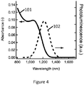
- Figure 4 shows a plot of the absorbance 101 and emission 102 of HgTe quantum dots suspended in trichloroethylene.
- the emission can be called photoluminescence. It is visible that the quantum dots 3 absorb exciting light 11 mainly below 1100 nm, which preferably corresponds to the first wavelength range, and emit light 12 mainly between 1100 nm and 1400 nm, which preferably corresponds to the second wavelength range.
- Figures 5a and 5b illustrate the light output of the 1 D amplifier (made by illuminating a stripe on the 2D PMMA/HgTe film) as a function of pump power ( Figure 5a ) and stripe length ( Figure 5b ).
- the exciting light 11 is at 447 nm.
- Figure 5a shows a plot 201 as function of the fluence of the exciting light 11.
- a power density threshold of 40 mW/cm 2 is extracted from this plot by fitting an exponential.
- Figure 5b shows a plot 202 of as function of the length of the optical gain medium 2.
- a net modal gain coefficient of 2.4 cm -1 is extracted from this plot by fitting an exponential 203.
- Figures 5a and 5b indicate a supralinear increase pointing towards light amplification of the type: exp(g(P)*L) where L is the stripe length pumped and g(P) is the gain (per cm, per mW) at a power of P.
- the supralinear output with pump power and increasing stripe length is a clear indication of light amplification.
- Figure 6a shows the photoluminescence intensity of a solid film obtained through dropcasting, containing 1 vol% HgTe quantum dots and 99 vol% polymer host after 700 nm excitation.
- the measured peak has two contributions.
- a first contribution 111 comes from quantum dots 3 following a radiative transition from the conduction band 22 to the valence band 21.
- the first contribution 111 comes from quantum dots 3 of a first type, which are intrinsic and show fast band-to-band decay.
- the wavelength range of first contribution 111 is the first wavelength range. Light in this first wavelength range is absorbed by the quantum dots 3.
- a second contribution 112 comes from quantum dots 3 following the transition scheme illustrated at Figures 2a and 2b .
- the second contribution 112 comes from quantum dots 3 of a second type, which have the band gap intermediate state 23 and fall back to the valence band 21 following the sub-bandgap transition and another transition.
- the wavelength range of second contribution 112 is the second wavelength range. Light in this second wavelength range is emitted by the quantum dots 3. It clearly appears that the contributions 111, 112 does not have their peak at the same wavelength. In other words, there is no linear absorption of the quantum dots 3 at the wavelengths of emission of the emitted light 12.
- Figure 6b shows the fraction of the second contribution to the total emission as function of the temperature. These values were extracted from plots equivalent to Figure 6a at various temperatures.
- Figure 7a shows a non-linear absorption spectra, taken 2.5 ns after photo-excitation for different pump fluences which correspond to different exciton densities ⁇ N>.
- the exciton density is equal to 0.3 for plot 103, 0.12 for plot 104, 0.06 for plot 105, 0.03 for plot 106 and 0.006 for plot 107.
- the delay of 2.5 ns strongly exceeds the lifetime of multi-excitons, such that quantum dots contain a single exciton at the most.
- Figure 7b shows the wavelength dependent gain threshold as obtained from the plots of Figure 7a.
- Figure 7b explicitly shows that HgTe quantum dots reach transparency at thresholds (N) dropping to 0.005 beyond 1450 nm.
- a threshold (N) value of 0.01 indicates that only one electron-hole pair per quantum dot out of hundred needs to be excited to get light amplification.
- Figure 8 illustrates the luminesce decay of the HgTe quantum dots dispersed in a solvent.
- the fast decay (480 ns) is due to direct transitions between levels 22 to 21 ( Figure 2a ) and the slow decay (several microseconds) is due to the transition from levels 22 to 23, i.e. the gain transition.
- the gain state is long lived, a requisite for achieving continuous wave gain.
- the inventors have analyzed the optical gain after repetitive washing of an optical gain medium 2 where the dispersion medium 4 is PMMA.
- HgTe quantum dots other quantum dots able to be excited by exciting light 11 in a first wavelength range corresponding to a transition 31 between the valence band 21 and the conduction band 22, and to amplify emitted light 12 in a second wavelength range corresponding to optically active electronic transition 32a, 32b, 33a, 33b involving a band gap intermediate state 23 which is unoccupied at equilibrium will exhibit similar characteristics as the HgTe quantum dots.
Landscapes
- Physics & Mathematics (AREA)
- Condensed Matter Physics & Semiconductors (AREA)
- General Physics & Mathematics (AREA)
- Electromagnetism (AREA)
- Optics & Photonics (AREA)
- Luminescent Compositions (AREA)
Abstract
The present invention relates to an optical gain medium (2) comprising colloidal semiconductor quantum dots (3) and a light amplification method using the optical gain medium (2). The quantum dots (3) are preferably HgTe quantum dots. The optical gain medium (2) can be pumped by continuous wave exciting light (11) at low power density. It can therefore be used to amplify sun light.
Description
- According to a first aspect, the present invention relates to a light amplification method. According to a second aspect, the present invention relates to an optical gain medium.
- In an optical gain medium, exciting light in a first wavelength range can be used as an optical pump in such a way that the medium emits and then amplifies light in a second wavelength range. The power density threshold of such an optical gain medium is defined as the minimum power density required to obtain optical gain.
- It is desirable, for example for solar panels, to have an optical gain medium where the sun light can be used as pumping light, and then be amplified. Such an optical gain medium should be able to work with an exciting light that is continuous wave light. Moreover, such an optical gain medium must have a low power density threshold since the total solar irradiance only amounts approximately to 100 mW/cm2, the total solar irradiance being the power per unit area of sunlight integrated over all wavelengths.
- The PhD thesis of Pieter Geiregat, called "Colloidal Quantum Dots for Guided Wave Photonics : from Optical Gain to Ultrafast Modulation", Universiteit Gent, 2015, discloses an optical gain medium comprising HgTe quantum dots that provides optical gain at low power density. This low power density threshold is explained by a model wherein a single electron in the conduction band is coupled to both the valence band and a band gap intermediate state. This model involves a transition of a conduction band electron to a band gap intermediate state that is empty in unexcited quantum dots or a transition of a valence band hole to an occupied band gap intermediate state that have no counterpart in absorption. This PhD thesis describes that the lifetime of the excited state that gives rise to the optical transition with the low power density threshold has been determined by measuring the decay of the luminescence signal at various time delays and has been found in the range 20 to 40 ns.
- Such a lifetime requires the excitation of many quantum dots at the same time to obtain amplification, which cannot be achieved by continuous wave pumping. Therefore, according to this PhD thesis, the HgTe quantum dots would be unable to provide amplification for continuous wave pumping at low power density. That would make the HgTe quantum dots unsuitable for amplification of solar light.
- Document
WO2015/186033 discloses a gain medium working with continuous wave pumping. The gain medium consists in a film of colloidal nanocrystals of semiconductor material. The nanocrystals are two-dimensional nanocrystals. Continuous wave light amplification occurs due to a biexciton gain mechanism. In the gain medium presented inWO2015/186033 , the power density threshold of the optical pump is equal to 6,5 W/cm2 for continuous wave pumping, which is too high to obtain amplification induced by solar light. - According to a first aspect, an object of the invention is to provide a light amplification method that can achieve continuous wave light amplification under low power density continuous wave optical pumping.
- According to this first aspect, the invention a light amplification method for amplifying light coming from a light source, the light amplification method comprising the steps of:
- (a) providing an optical gain medium comprising colloidal semiconductor quantum dots having a band gap intermediate state between a valence band and a conduction band, the band gap intermediate state being unoccupied at equilibrium, the quantum dots being able to be excited by exciting light in a first wavelength range corresponding to a transition between the valence band and the conduction band, and to amplify emitted light in a second wavelength range corresponding to an optically active electronic transition involving the band gap intermediate state, the wavelengths in the second wavelength range being higher than the wavelengths in the first wavelength range,
- (b) receiving, from said light source and with said gain medium, exciting light in the first wavelength range to generate a transition from the valence band to the conduction band,
- (c) emitting, with said gain medium, emitted light in the second wavelength range by a transition involving the band gap intermediate state,
- The optically active electronic transition involving the band gap intermediate state can be called a sub-bandgap transition. It involves a difference of energy lower than the band gap transition. It can be a transition between the conduction band and the band gap intermediate state, between the band gap intermediate state and the valence band or between the band gap intermediate state and a second band gap intermediate state.
- The inventors have shown that the power density threshold for the amplification of spontaneous emission under continuous wave light excitation by colloidal semiconductor quantum dots having such a sub-bandgap transition can be as low as 40 mW/cm2, which is considerably better than the power density threshold of 6,5 W/cm2 indicated in document
WO2015/186033 . Colloidal semiconductor quantum dots having a sub-bandgap transition are therefore able to meet the requirements for emission induced by solar light and for DC electrical pumping. Moreover, a modal gain of up to 2.1 cm-1 in a optical gain medium comprising such quantum dots was demonstrated by the inventors under continuous wave light excitation and under pulsed excitation, the modal gain being the gain achieved by the guided optical mode of the photonic structure. The material gain can be substantially higher due to low confinement of the guided mode in the quantum dot-enriched region of the slab. - Amplification of continuous wave light by the quantum dots is possible because of the sub-bandgap transition and because the lifetime of the excited state that gives rise to the optically active sub-bandgap transition with the low power density threshold can be around 28 µs, which is much longer than the lifetime of 20 to 40 ns disclosed in the PhD of Pieter Geigerat. It is therefore possible to achieve, with continuous wave pumping, excitation of enough quantum dots to obtain amplification.
- The inventors can explain the long lifetime of the excited state by a model involving two types of quantum dots. The quantum dots of the first type are intrinsic and show fast band-to-band decay. They do not contribute to the light amplification. The quantum dots of the second type have the band gap intermediate state and fall back to the valence band following the sub-bandgap transition and another transition. This other transition can be non-radiative. For example, a non-radiative transition can bring the quantum dot from the conduction band to the band gap intermediate state having a long lifetime and then the optically active sub-bandgap transition can happen between the band gap intermediate state and the valence band. This model is fundamentally different from the model disclosed in the PhD of Pieter Geigerat wherein a single electron in the conduction band is coupled together to the valence band and to the band gap intermediate state.
- Actually, the inventors have shown that in such quantum dots, excitation to the conduction band caused by continuous wave light is followed by the spontaneous emission of light through the sub-bandgap transition. Since the band gap intermediate state is unoccupied at equilibrium, the sub-bandgap transition occurs at wavelengths where the quantum dots are transparent, meaning that the emitted light is not reabsorbed by the quantum dots. The emitted light can then generate stimulated emission in another quantum dot, which creates optical amplification. As a result, stimulated emission involving this transition leads to net optical gain as attested, for example, by the amplification of the spontaneous emission at very low levels of pumping power.
- The fact that colloidal semiconductor quantum dots can provide such a low power density threshold and a good modal gain is surprising. Typically, stimulated emission across the band-gap transition is utilized to achieve optical amplification. Since these band-edge states are degenerate, quantum dots must contain more than one exciton on average to achieve population inversion. Next to this intrinsic drawback of 2-level gain media, multi-excitons rapidly recombine through non-radiative Auger processes, which limits the population inversion lifetime to a few tens of picoseconds. This makes that optical amplification is mostly only achieved using femtosecond pulsed illumination. All this indicates that quantum dots are not expected to provide good optical amplification characteristics.
- The band gap intermediate state is due to the presence of defects in the crystal structure or ill passivated sites at the quantum dot surface that create a surface-localized gap state. Such defects or ill passivated sites are often seen as disadvantageous for the optical properties of colloidal quantum dots. For example, the extend of surface passivation has been explicitly linked to a low photoluminenescence quantum yield of colloidal quantum dots. From a similar perspective,
US6819692B2 emphasizes that optical gain characteristics of nanocrystal solids will be better with longer non-radiative lifetime of multi-excitons. Hence, defects that trap electrons or holes are generally expected to be disadvantageous for optical gain. - An advantage of colloidal quantum dots is that the emission wavelength can be tuned by tuning the size of the quantum dots. Another advantage is that the colloidal quantum dots are easy and cheap to produce.
- An advantage of continuous wave excitation over pulsed excitation is that the amplification happens continuously instead of happening by pulses.
- In an embodiment of the invention, the exciting light received at step (b) has a power density below 1 W/cm2, preferably below 100 mW/cm2, more preferably below 50 mW/cm2.
- In an embodiment of the invention, the quantum dots comprise ZnO, ZnS, ZnSe, ZnTe, CdO, CdS, CdSe, CdTe, MgO, MgS, MgSe, MgTe, HgO, HgS, HgSe, HgTe, AlN, AlP, AlAs, AlSb, GaN, GaP, GaAs, GaSb, InN, InP, InAs, InSb, TIN, TIP, TlAs, TlSb, TlSb, PbS, PbSe, PbTe, or mixtures thereof.
- In an embodiment of the invention, the quantum dots comprise HgTe, preferably are HgTe quantum dots.
- In an embodiment of the invention, the band gap intermediate state is a surface-localized gap state. It is especially advantageous because the amplification can be tuned by washing the optical gain medium.
- According to a second aspect, the invention provides an optical gain medium comprising colloidal semiconductor quantum dots having a band gap intermediate state between a valence band and a conduction band, the band gap intermediate state being unoccupied at equilibrium, the quantum dots being able to be excited by exciting light in a first wavelength range corresponding to a transition between the valence band and the conduction band, and to amplify emitted light in a second wavelength range corresponding to an optically active electronic transition involving the band gap intermediate state, the wavelengths in the second wavelength range being higher than the wavelengths in the first wavelength range.
- Any embodiment of an optical gain medium described in the present document can be used in the light amplification method according to the invention.
- In an embodiment of the invention, the quantum dots comprise ZnO, ZnS, ZnSe, ZnTe, CdO, CdS, CdSe, CdTe, MgO, MgS, MgSe, MgTe, HgO, HgS, HgSe, HgTe, AlN, AlP, AlAs, AlSb, GaN, GaP, GaAs, GaSb, InN, InP, InAs, InSb, TlN, TlP, TlAs, TlSb, TlSb, PbS, PbSe, PbTe, or mixtures thereof.
- In an embodiment of the invention, the quantum dots comprise HgTe, preferably are HgTe quantum dots.
- In an embodiment of the invention, the quantum dots have an average diameter between 1 and 20 nm, preferably between 2 and 10 nm, more preferably between 3.0 and 4.0 nm.
- In an embodiment of the invention, the dispersion medium is a liquid, for example toluene. It makes possible to give any shape to the optical gain medium.
- In an embodiment of the invention, the dispersion medium is a flexible solid. It makes the optical gain medium especially solid and easy to handle.
- The invention also provides a luminescent solar concentrator comprising the optical gain medium according to an embodiment of the invention.
- In an embodiment of the invention, the optical gain medium is arranged for receiving continuous wave exciting light, for example continuous wave light coming from the sun, from a first direction and to emit amplified light in a second direction, and the luminescent solar concentrator comprises an output device arranged in the second direction to receive the light emitted by the optical gain medium. The second direction is different from the first direction. The second direction may be essentially perpendicular to the first direction.
- In an embodiment of the invention, the output device comprises a photovoltaic cell.
- The invention also provides a light emitting device comprising:
- an optical gain medium according to an embodiment of the invention, and
- a continuous wave light source arranged to provide continuous wave exciting light in the first wavelength range to the optical gain medium.
- In an embodiment of the invention, the continuous wave light source is arranged to provide light at a power density below 1 W/cm2, preferably below 100 mW/cm2, even more preferably below 50 W/cm2.
- The invention also provides a laser comprising:
- an optical cavity,
- a light emitting device according to an embodiment of the invention, wherein the optical gain medium is arranged inside the optical cavity. The invention also provides an electronic circuit comprising:
- a connecting device comprising a light emitting device according to an embodiment of the invention, and
- an electronic device arranged to receive the light emitted by the connecting device.
- For a better understanding of the present invention, reference will now be made, by way of example, to the accompanying drawings in which:
-
Figure 1 schematically illustrates a light source and an optical gain medium according to an embodiment of the invention, -
Figure 2a schematically illustrates a spontaneous emission andFigure 2b schematically illustrates a stimulated emission according to an embodiment of the invention. -
Figure 3a schematically illustrates a spontaneous emission andFigure 3b schematically illustrates a stimulated emission according to an embodiment of the invention, -
Figure 4 shows a plot of the absorbance and emission of HgTe quantum dots suspended in trichloroethylene, -
Figure 5a illustrates the light output versus optically pumped pump power for an embodiment of the invention where the quantum dots are HgTe quantum dots and the dispersion medium is PMMA, -
Figure 5b illustrates the light output versus stripe length of the device for an embodiment of the invention where the quantum dots are HgTe quantum dots and the dispersion medium is PMMA, -
Figure 6a shows the photoluminescence intensity of a solid film obtained through dropcasting, containing 1 vol% HgTe quantum dots and 99 vol% polymer host, -
Figure 6b shows the fraction of the second contribution to the total emission as function of the temperature, -
Figure 7a shows a non-linear absorption spectra, taken 2.5 ns after photo-excitation for different pump fluences which correspond to different exciton densities <N> in an embodiment of the invention where the quantum dots are HgTe quantum dots, -
Figure 7b shows the wavelength dependent gain threshold as obtained from the plots ofFigure 7a , -
Figure 8 illustrates the luminesce decay of the HgTe quantum dots dispersed in a solvent, and -
Figure 9 shows the gain cross section and the photoluminescent quantum yield as function of the number of washing steps for an embodiment of the invention where the quantum dots are HgTe quantum dots and the dispersion medium is PMMA. - The present invention will be described with respect to particular embodiments and with reference to certain drawings but the invention is not limited thereto. The drawings described are only schematic and are nonlimiting. In the drawings, the size of some of the elements may be exaggerated and not drawn on scale for illustrative purposes.
- Furthermore, the terms first, second, third and the like in the description and in the claims, are used for distinguishing between similar elements and not necessarily for describing a sequential or chronological order. The terms are interchangeable under appropriate circumstances and the embodiments of the invention can operate in other sequences than described or illustrated herein.
- Furthermore, the various embodiments, although referred to as "preferred" are to be construed as exemplary manners in which the invention may be implemented rather than as limiting the scope of the invention.
- The term "comprising", used in the claims, should not be interpreted as being restricted to the elements or steps listed thereafter; it does not exclude other elements or steps. It needs to be interpreted as specifying the presence of the stated features, integers, steps or components as referred to, but does not preclude the presence or addition of one or more other features, integers, steps or components, or groups thereof. Thus, the scope of the expression "a device comprising A and B" should not be limited to devices consisting only of components A and B, rather with respect to the present invention, the only enumerated components of the device are A and B, and further the claim should be interpreted as including equivalents of those components.
- On the figures, identical or analogous elements may be referred by a same number.
- In the frame of the present document, a "continuous wave light" is a light which is continuous in time over a period of at least 30 µs, preferably at least one second, more preferably at least 60 seconds..
- In the frame of the present document, the "optical gain", g, is the the increase of light intensity I per unit of propagation length L. It is such as

- In the frame of the present document, a "state unoccupied at equilibrium" is an energy state which cannot be reached without excitation at temperature below the equilibrium temperature of the system.
- In the frame of the present document, the "exciton density", noted <N>, is defined as the average number of electron-hole pairs per quantum dot, either at time zero for pulsed excitation, or as time-averaged for the continuous wave experiments. The probability to have N electron-hole pairs is expected to be given by a Poisson distribution with mean <N>, i.e. P(N) = exp(-<N>) <N>N/N!.
- In the frame of the present document, the "gain threshold", also called the threshold <N> is , for every wavelength, defined as the average number of electron-hole pairs per quantum dot needed to achieve transparency (zero absorbance or a perfect balance between absorption and stimulated emission) at that wavelength.
-
Figure 1 schematically illustrates alight source 1 emitting continuous wave light, which is anexciting light 11, and anoptical gain medium 2 comprising colloidalsemiconductor quantum dots 3 and adispersion medium 4. Theoptical gain medium 2 receives theexciting light 11 and, in response to theexciting light 11, emits amplified emittedlight 12. - In an embodiment of the invention, the
light source 1 is a device. In that case, thelight source 1 and theoptical gain medium 2 can be part of a light emitting device according to the invention. In another embodiment of the invention, thelight source 1 is the sun. - The
exciting light 11, which can be called pumping light, is in a first wavelength range. The first wavelength range is preferably at least partially below 1250 nm, more preferably totally below 1250 nm. The first wavelength range preferably corresponds to wavelengths that are absorbed by thequantum dots 3. The first wavelength range preferably corresponds to a range of energy higher than the band gap of thequantum dots 3. - The
quantum dots 3 have preferably an average diameter between 1 and 20 nm, more preferably between 2 and 10 nm, even more preferably between 3.0 and 4.0 nm. - The
quantum dots 3 preferably comprises ZnO, ZnS, ZnSe, ZnTe, CdO, CdS, CdSe, CdTe, MgO, MgS, MgSe, MgTe, HgO, HgS, HgSe, HgTe, AlN, AlP, AlAs, AlSb, GaN, GaP, GaAs, GaSb, InN, InP, InAs, InSb, TlN, TlP, TlAs, TlSb, TlSb, PbS, PbSe, PbTe or mixtures thereof. - The
quantum dots 3 are preferably ZnO, ZnS, ZnSe, ZnTe, CdO, CdS, CdSe, CdTe, MgO, MgS, MgSe, MgTe, HgO, HgS, HgSe, HgTe, AlN, AlP, AlAs, AlSb, GaN, GaP, GaAs, GaSb, InN, InP, InAs, InSb, TlN, TlP, TlAs, TlSb, TlSb, PbS, PbSe, PbTe quantum dots or mixtures thereof. - The
quantum dots 3 are dispersed in thedispersion medium 4. In an embodiment of the invention, thedispersion medium 4 is a liquid, for example toluene. In an embodiment of the invention, thedispersion medium 4 is a flexible solid, for example a PMMA (polymethyl-methacrylate) film. In that case, theoptical gain medium 2 comprises a nanocomposite made of the flexible solid and thequantum dots 3. - The emitted
light 12 is generated and then amplified by thequantum dots 3. The emittedlight 12 has a longer wavelength than theexciting light 11. The emittedlight 12 is in a second wavelength range. The wavelengths in the second wavelength range are higher than the wavelengths in the first wavelength range. The second wavelength range is preferably at least partially between 1100 nm and 1400 nm. - The
dispersion medium 4 is preferably transparent in the first and the second wavelength ranges. - The
quantum dots 3 do not absorb light in the second wavelength range because the band gapintermediate state 23 is empty at equilibrium. This will be described with reference toFigures 2 and 3 . - If the
light source 1 is the sun, theoptical gain medium 2 is preferably comprised in a luminescent light concentrator. The luminescent light concentrator also preferably comprises an output device, which can comprise a photovoltaic cell. In an embodiment of the invention, theoptical gain medium 2 is arranged for receiving continuous wave light 11 coming from the sun from a first direction and to emit amplified light in a second direction, and the output device is arranged in the second direction to receive the light 12 emitted by the optical gain medium. -
Figure 2a schematically illustrates aspontaneous emission 32a andFigure 2b schematically illustrates a stimulatedemission 33a according to an embodiment of the invention.Figure 3a schematically illustrates aspontaneous emission 32b andFigure 3b schematically illustrates a stimulatedemission 33b according to an embodiment of the invention. - The
quantum dots 3 have a band gap between theirvalence band 21 and theirconduction band 22. Thevalence band 21 comprises a plurality of energy states 41. Theconduction band 22 comprises a plurality of energy states 42. A band gapintermediate state 23 is present in the band gap. The band gapintermediate state 23 is far enough from thevalence band 21 to be unoccupied at equilibrium. - At equilibrium, the
conduction band 22 is empty. Theexciting light 11 excites an electron of thequantum dot 3 to theconduction band 22 by apumping transition 31. - In the embodiment of the invention illustrated at
Figure 2a , an electron in a firstquantum dot 3 goes down to the band gapintermediate state 23 by a spontaneous emission, which is an optically activeelectronic transition 32a. Thisspontaneous emission 32a generates emittedlight 12. Then, as illustrated atFigure 2b , an electron in a secondquantum dot 3 goes down to the band gapintermediate state 23 by a stimulated emission, which is an optically activeelectronic transition 33a. This stimulatedemission 33a is caused by the light 12 emitted by the spontaneous emission of the firstquantum dot 3 and received by the secondquantum dot 3. The stimulatedemission 33a results in two photons of emittedlight 12. Therefore, as a result, the emittedlight 12 is amplified by the second quantum dots. Later, the electron will go back to thevalence band 21 by a further transition, which may be radiative or non-radiative. - In the case illustrated by
Figures 2a and 2b , the optically activeelectronic transition intermediate state 23 is the transition between theconduction band 22 and the band gapintermediate state 23. The excited state that gives rise to the optically activeelectronic transition conduction band 22. - In the embodiment of the invention illustrated at
Figure 3a , an electron in a firstquantum dot 3 goes down to the band gapintermediate state 23 by a first transition, which may be radiative or non-radiative. Then, the electron goes down the band gapintermediate state 23 by a spontaneous emission, which is an optically activeelectronic transition 32b. Thisspontaneous emission 32b generates emittedlight 12. Then, as illustrated atFigure 3b , an electron in a secondquantum dot 3 goes down from the band gapintermediate state 23 to thevalence band 21 by a stimulated emission, which is an optically activeelectronic transition 33b. The stimulatedemission 33b is due to the light 12 emitted by the spontaneous emission of the firstquantum dot 3. The stimulatedemission 33b results in two photons of emitted 12. Therefore, as a result, the emittedlight 12 is amplified by the secondquantum dot 3. - In the case illustrated by
Figures 3a and 3b , the optically activeelectronic transition intermediate state 23 is the transition between the band gapintermediate state 23 and one of the energy states 41 of thevalence band 21. The excited state that gives rise to the optically activeelectronic transition intermediate state 23. - It is also possible that the optically active electronic transition involving the band gap
intermediate state 23 is a transition between the band gapintermediate state 23 and a lower band gap intermediate state. - Since the band gap
intermediate state 23 is unoccupied at equilibrium, there is no absorption at the wavelength of the emittedlight 12. - The
quantum dots 3 used in the experiments resulting in the plots illustrated in theFigures 4 to 9 are HgTe quantum dots that were prepared with the following process. - 270 mg (1 mmol) of HgCl2, 1.6 mL (6 mmol) of dodecanethiol (DDT) and 8 mL of oleylamine (OLA) were mixed in a 25 mL flask and degassed under vacuum at 100°C for one hour, after which the reaction mixture was placed under nitrogen while keeping the temperature at 60°C. Next, 1 mL of a 1 M solution of tellurium in tri-octylphosphine was rapidly injected and a black-colored reaction mixture was obtained within a few seconds. The reaction mixture was kept at the injection temperature to allow for quantum dot growth for 1 minute (1220 nm emission) to 3 minutes (1300 nm emission), after which the reaction was quenched by injecting 10 mL of toluene and cooling with a water bath. As obtained HgTe quantum dots were purified twice using toluene and methanol.
- In the case where the
dispersion medium 4 is a flexible solid, the following further steps were used. PMMA (polymethyl-methacrylate) with a molecular weight of 120,000 and a mass density of 1.19 g/cm3 was used. 0.96 g of PMMA was dissolved in 10 mL of toluene to obtain a 5 m% solution. From this stock solution, 1 mL was mixed with a given HgTe quantum dot solution in toluene to obtain a volume fraction of quantum dots of 0.1 to 1 % relative to PMMA. These composites were dropcast or spincoated on glass substrates to achieve different film thicknesses of a few 100 nm to several 100 µm. For the ASE/VSL measurements the films were delaminated, yielding a flexible and free-standing hybrid polymer/quantum dot lightguide and put on a support. -
Figure 4 shows a plot of theabsorbance 101 andemission 102 of HgTe quantum dots suspended in trichloroethylene. The emission can be called photoluminescence. It is visible that thequantum dots 3 absorbexciting light 11 mainly below 1100 nm, which preferably corresponds to the first wavelength range, and emit light 12 mainly between 1100 nm and 1400 nm, which preferably corresponds to the second wavelength range. -
Figures 5a and 5b illustrate the light output of the 1 D amplifier (made by illuminating a stripe on the 2D PMMA/HgTe film) as a function of pump power (Figure 5a ) and stripe length (Figure 5b ). Theexciting light 11 is at 447 nm.Figure 5a shows aplot 201 as function of the fluence of theexciting light 11. A power density threshold of 40 mW/cm2 is extracted from this plot by fitting an exponential.Figure 5b shows aplot 202 of as function of the length of theoptical gain medium 2. A net modal gain coefficient of 2.4 cm-1 is extracted from this plot by fitting an exponential 203.Figures 5a and 5b indicate a supralinear increase pointing towards light amplification of the type: exp(g(P)*L) where L is the stripe length pumped and g(P) is the gain (per cm, per mW) at a power of P. The supralinear output with pump power and increasing stripe length is a clear indication of light amplification. -
Figure 6a shows the photoluminescence intensity of a solid film obtained through dropcasting, containing 1 vol% HgTe quantum dots and 99 vol% polymer host after 700 nm excitation. The measured peak has two contributions. Afirst contribution 111 comes fromquantum dots 3 following a radiative transition from theconduction band 22 to thevalence band 21. In other words, thefirst contribution 111 comes fromquantum dots 3 of a first type, which are intrinsic and show fast band-to-band decay. The wavelength range offirst contribution 111 is the first wavelength range. Light in this first wavelength range is absorbed by thequantum dots 3. Asecond contribution 112 comes fromquantum dots 3 following the transition scheme illustrated atFigures 2a and 2b . In other words, thesecond contribution 112 comes fromquantum dots 3 of a second type, which have the band gapintermediate state 23 and fall back to thevalence band 21 following the sub-bandgap transition and another transition. The wavelength range ofsecond contribution 112 is the second wavelength range. Light in this second wavelength range is emitted by thequantum dots 3. It clearly appears that thecontributions quantum dots 3 at the wavelengths of emission of the emittedlight 12. -
Figure 6b shows the fraction of the second contribution to the total emission as function of the temperature. These values were extracted from plots equivalent toFigure 6a at various temperatures. -
Figure 7a shows a non-linear absorption spectra, taken 2.5 ns after photo-excitation for different pump fluences which correspond to different exciton densities <N>. The exciton density is equal to 0.3 forplot 103, 0.12 for plot 104, 0.06 forplot 105, 0.03 forplot 106 and 0.006 forplot 107. The delay of 2.5 ns strongly exceeds the lifetime of multi-excitons, such that quantum dots contain a single exciton at the most. -
Figure 7b shows the wavelength dependent gain threshold as obtained from the plots ofFigure 7a. Figure 7b explicitly shows that HgTe quantum dots reach transparency at thresholds (N) dropping to 0.005 beyond 1450 nm. A threshold (N) value of 0.01 indicates that only one electron-hole pair per quantum dot out of hundred needs to be excited to get light amplification. -
Figure 8 illustrates the luminesce decay of the HgTe quantum dots dispersed in a solvent. The fast decay (480 ns) is due to direct transitions betweenlevels 22 to 21 (Figure 2a ) and the slow decay (several microseconds) is due to the transition fromlevels 22 to 23, i.e. the gain transition. Clearly, the gain state is long lived, a requisite for achieving continuous wave gain. - To further identify the origin of the gap states involved, the inventors have analyzed the optical gain after repetitive washing of an
optical gain medium 2 where thedispersion medium 4 is PMMA. - Repetitive washing is known to displace surface passivating moieties, induce dangling bonds at the quantum dots surface and reduce the photoluminescent quantum yield (PLQY), which is the ratio between the number of photons emitted and absorbed by the quantum dots. As illustrated at
Figure 9 , the inventors have found that increased washing yields a strong increase in thegain cross section 121 and a concomitant decrease inPLQY 122. This seems to indicate that the optically active electronic transition involves a band gapintermediate state 23 at the HgTe surface, possibly created by Te dangling bonds after Hg-thiolate removal upon washing. The gain cross section is related to the material gain gi as: gi x volume = cross section. - Even if the present document mainly refers to HgTe quantum dots, other quantum dots able to be excited by
exciting light 11 in a first wavelength range corresponding to atransition 31 between thevalence band 21 and theconduction band 22, and to amplify emitted light 12 in a second wavelength range corresponding to optically activeelectronic transition intermediate state 23 which is unoccupied at equilibrium will exhibit similar characteristics as the HgTe quantum dots. - Although the present invention has been described above with respect to particular embodiments, it will readily be appreciated that other embodiments are also possible.
Claims (16)
- Light amplification method for amplifying light coming from a light source (1), the light amplification method comprising the steps of:(a) providing an optical gain medium (2) comprising colloidal semiconductor quantum dots (3) having a band gap intermediate state (23) between a valence band (21) and a conduction band (22), the band gap intermediate state (23) being unoccupied at equilibrium, the quantum dots (3) being able to be excited by exciting light (11) in a first wavelength range corresponding to a transition (31) between the valence band (21) and the conduction band (22), and to amplify emitted light (12) in a second wavelength range corresponding to an optically active electronic transition (32a, 32b, 33a, 33b) involving the band gap intermediate state (23), the wavelengths in the second wavelength range being higher than the wavelengths in the first wavelength range,(b) receiving, from said light source (1) and with said gain medium (2), exciting light (11) in the first wavelength range to generate a transition (31) from the valence band (21) to the conduction band (22),(c) emitting, with said gain medium (2), emitted light (12) in the second wavelength range by a transition (32a, 32b, 33a, 33b) involving the band gap intermediate state (23),characterized in that the exciting light (11) received at step (b) is a continuous wave light.
- Light amplification method according to claim 1, characterized in that the exciting light (11) received at step (b) has a power density below 1 W/cm2, preferably below 100 mW/cm2, more preferably below 50 mW/cm2.
- Light amplification method according to claim 1 or 2, characterized in that the quantum dots (3) comprise ZnO, ZnS, ZnSe, ZnTe, CdO, CdS, CdSe, CdTe, MgO, MgS, MgSe, MgTe, HgO, HgS, HgSe, HgTe, AlN, AlP, AlAs, AlSb, GaN, GaP, GaAs, GaSb, InN, InP, InAs, InSb, TlN, TlP, TlAs, TlSb, TlSb, PbS, PbSe, PbTe, or mixtures thereof.
- Light amplification method according to the preceding claim, characterized in that the quantum dots (3) comprise HgTe, preferably are HgTe quantum dots.
- Light amplification method according to any of the preceding claims, characterized in that the band gap intermediate state (23) is a surface-localized gap state.
- Optical gain medium (2) comprising colloidal semiconductor quantum dots (3) having a band gap intermediate state (23) between a valence band (21) and a conduction band (22), the band gap intermediate state (23) being unoccupied at equilibrium, the quantum dots (3) being able to be excited by exciting light (11) in a first wavelength range corresponding to a transition (31) between the valence band (21) and the conduction band (22), and to amplify emitted light (12) in a second wavelength range corresponding to an optically active electronic transition (32a, 32b, 33a, 33b) involving the band gap intermediate state (23), the wavelengths in the second wavelength range being higher than the wavelengths in the first wavelength range.
- Optical gain medium (2) according to the preceding claim, characterized in that the quantum dots (3) comprise ZnO, ZnS, ZnSe, ZnTe, CdO, CdS, CdSe, CdTe, MgO, MgS, MgSe, MgTe, HgO, HgS, HgSe, HgTe, AlN, AlP, AlAs, AlSb, GaN, GaP, GaAs, GaSb, InN, InP, InAs, InSb, TlN, TlP, TlAs, TlSb, TlSb, PbS, PbSe, PbTe, or mixtures thereof.
- Optical gain medium (2) according to the preceding claim, characterized in that the quantum dots (3) comprise HgTe, preferably are HgTe quantum dots.
- Optical gain medium (2) according to any of claims 6 to 8, characterized in that the quantum dots (3) have an average diameter between 1 and 20 nm, preferably between 2 and 10 nm, more preferably between 3.0 and 4.0 nm.
- Optical gain medium according to any of claims 6 to 9, characterized in that the dispersion medium (4) is a liquid, for example toluene.
- Optical gain medium according to any of claims 6 to 9, characterized in that the dispersion medium (4) is a flexible solid.
- Luminescent solar concentrator comprising the optical gain medium (2) according to any of claims 6 to 11.
- Luminescent solar concentrator according to the preceding claim wherein the optical gain medium (2) is arranged for receiving continuous wave exciting light (11), for example continuous wave light coming from the sun, from a first direction and to emit amplified light (12) in a second direction, and comprising an output device arranged in the second direction to receive the light (12) emitted by the optical gain medium (2).
- Luminescent solar concentrator according to the preceding claim, characterized in that the output device comprises a photovoltaic cell.
- Light emitting device comprising:• an optical gain medium according to any of claims 6 to 11, and• a continuous wave light source (1) arranged to provide continuous wave exciting light (11) in the first wavelength range to the optical gain medium (2).
- Light emitting device according to the preceding claim, characterized in that the continuous wave light source (1) is arranged to provide light (11) at a power density below 1 W/cm2, preferably below 100 mW/cm2, more preferably below 50 mW/cm2.
Priority Applications (1)
| Application Number | Priority Date | Filing Date | Title |
|---|---|---|---|
| EP17170479.4A EP3402018A1 (en) | 2017-05-10 | 2017-05-10 | Light amplification method using an optical gain medium comprising quantum dots |
Applications Claiming Priority (1)
| Application Number | Priority Date | Filing Date | Title |
|---|---|---|---|
| EP17170479.4A EP3402018A1 (en) | 2017-05-10 | 2017-05-10 | Light amplification method using an optical gain medium comprising quantum dots |
Publications (1)
| Publication Number | Publication Date |
|---|---|
| EP3402018A1 true EP3402018A1 (en) | 2018-11-14 |
Family
ID=58701491
Family Applications (1)
| Application Number | Title | Priority Date | Filing Date |
|---|---|---|---|
| EP17170479.4A Withdrawn EP3402018A1 (en) | 2017-05-10 | 2017-05-10 | Light amplification method using an optical gain medium comprising quantum dots |
Country Status (1)
| Country | Link |
|---|---|
| EP (1) | EP3402018A1 (en) |
Citations (2)
| Publication number | Priority date | Publication date | Assignee | Title |
|---|---|---|---|---|
| US6819692B2 (en) | 2000-03-14 | 2004-11-16 | Massachusetts Institute Of Technology | Optical amplifiers and lasers |
| WO2015186033A1 (en) | 2014-06-03 | 2015-12-10 | Fondazione Istituto Italiano Di Tecnologia | Continuous-wave pumped colloidal nanocrystal laser |
-
2017
- 2017-05-10 EP EP17170479.4A patent/EP3402018A1/en not_active Withdrawn
Patent Citations (2)
| Publication number | Priority date | Publication date | Assignee | Title |
|---|---|---|---|---|
| US6819692B2 (en) | 2000-03-14 | 2004-11-16 | Massachusetts Institute Of Technology | Optical amplifiers and lasers |
| WO2015186033A1 (en) | 2014-06-03 | 2015-12-10 | Fondazione Istituto Italiano Di Tecnologia | Continuous-wave pumped colloidal nanocrystal laser |
Non-Patent Citations (5)
| Title |
|---|
| BARBOSA: "Luminescence of PbS quantum dots on a silica microstructured fiber", SPIE, PO BOX 10 BELLINGHAM WA 98227-0010 USA, 2010, XP040523666 * |
| CHAO LIU ET AL: "Novel nano-structured glasses containing semiconductor quantum dots: controlling the photoluminescence with phonons and photons", JOURNAL OF MATERIALS SCIENCE: MATERIALS IN ELECTRONICS, KLUWER ACADEMIC PUBLISHERS, BO, vol. 20, no. 1, 11 March 2008 (2008-03-11), pages 282 - 285, XP019644548, ISSN: 1573-482X * |
| CHENG CHENG ET AL: "Experimental Realization of a PbSe-Quantum-Dot Doped Fiber Laser", IEEE PHOTONICS TECHNOLOGY LETTERS, IEEE SERVICE CENTER, PISCATAWAY, NJ, US, vol. 25, no. 6, 1 March 2013 (2013-03-01), pages 572 - 575, XP011495787, ISSN: 1041-1135, DOI: 10.1109/LPT.2013.2243139 * |
| M. R. HUMMON ET AL: "Measuring charge trap occupation and energy level in CdSe/ZnS quantum dots using a scanning tunneling microscope", PHYSICAL REVIEW. B, CONDENSED MATTER AND MATERIALS PHYSICS, vol. 81, no. 11, 1 March 2010 (2010-03-01), US, pages 115439 - 1, XP055225254, ISSN: 1098-0121, DOI: 10.1103/PhysRevB.81.115439 * |
| PIETER GEIREGAT: "Colloidal quantum dots for guided wave photonics : from optical gain to ultrafast modulation -Dissertation", 2015, GHENT UNIVERSITY. FACULTY OF ENGINEERING AND ARCHITECTURE ; FACULTY OF SCIENCES, ISBN: 9789085787662, pages: Frontpg-XXV, 1 - 259, XP002776627 * |
Similar Documents
| Publication | Publication Date | Title |
|---|---|---|
| Malko et al. | From amplified spontaneous emission to microring lasing using nanocrystal quantum dot solids | |
| Moreels et al. | Nearly Temperature‐Independent Threshold for Amplified Spontaneous Emission in Colloidal CdSe/CdS Quantum Dot‐in‐Rods | |
| Wang et al. | Light emission and amplification in charged CdSe quantum dots | |
| Klimov et al. | Ultrafast carrier dynamics in semiconductor quantum dots | |
| Frolov et al. | Cooperative emission in π-conjugated polymer thin films | |
| Reynolds et al. | Optically pumped ultraviolet lasing from ZnO | |
| Seilmeier et al. | Intersubband relaxation in GaAs-Al x Ga 1− x As quantum well structures observed directly by an infrared bleaching technique | |
| US5434878A (en) | Optical gain medium having doped nanocrystals of semiconductors and also optical scatterers | |
| Butty et al. | Room temperature optical gain in sol‐gel derived CdS quantum dots | |
| Klimov et al. | Ultrafast carrier dynamics, optical amplification, and lasing in nanocrystal quantum dots | |
| Lin et al. | Backward Raman amplification and pulse steepening in silica fibers | |
| Nootz et al. | Size dependence of carrier dynamics and carrier multiplication in PbS quantum dots | |
| US7778301B2 (en) | Cadmium sulfide quantum dot lasing in room temperature liquid solution | |
| Lingk et al. | Dynamics of amplified spontaneous emission in InAs/GaAs quantum dots | |
| Kushida et al. | Effects of excitation-induced optical absorption in highly excited semiconductors | |
| Capasso et al. | Conversion of Poisson photons into sub-Poisson photons by the action of electron feedback | |
| Lagatsky et al. | PbS quantum-dot-doped glass for efficient passive mode locking in a CW Yb: KYW laser | |
| Bakker et al. | Single-pass gain measurements on optically pumped Al x Ga (1-x) As-Al y Ga (1-y) As double-heterojunction laser structures at room temperature | |
| Hwang et al. | Effect of glass electronic states on carrier dynamics in semiconductor quantum-dot structures | |
| Mitra et al. | Ultraviolet laser emission from optically pumped ZnO | |
| US4378599A (en) | Semiconductor laser having broadband laser gain | |
| Masumoto | Luminescence and lasing of CuCl nanocrystals | |
| Saad et al. | Effect of temperature and pumping power on the photoluminescence properties of type-II CdTe/CdSe core-shell QDs | |
| Dang et al. | Very low threshold of amplified spontaneous emission in II–VI colloidal quantum dots at low exciton number | |
| Vogelgesang et al. | Wavelength-dependent optical degradation of green II–VI laser diodes |
Legal Events
| Date | Code | Title | Description |
|---|---|---|---|
| PUAI | Public reference made under article 153(3) epc to a published international application that has entered the european phase |
Free format text: ORIGINAL CODE: 0009012 |
|
| STAA | Information on the status of an ep patent application or granted ep patent |
Free format text: STATUS: THE APPLICATION HAS BEEN PUBLISHED |
|
| AK | Designated contracting states |
Kind code of ref document: A1 Designated state(s): AL AT BE BG CH CY CZ DE DK EE ES FI FR GB GR HR HU IE IS IT LI LT LU LV MC MK MT NL NO PL PT RO RS SE SI SK SM TR |
|
| AX | Request for extension of the european patent |
Extension state: BA ME |
|
| STAA | Information on the status of an ep patent application or granted ep patent |
Free format text: STATUS: THE APPLICATION IS DEEMED TO BE WITHDRAWN |
|
| 18D | Application deemed to be withdrawn |
Effective date: 20190515 |