EP3401717A1 - Optical receptacle, optical module, and measurement method - Google Patents
Optical receptacle, optical module, and measurement method Download PDFInfo
- Publication number
- EP3401717A1 EP3401717A1 EP16883759.9A EP16883759A EP3401717A1 EP 3401717 A1 EP3401717 A1 EP 3401717A1 EP 16883759 A EP16883759 A EP 16883759A EP 3401717 A1 EP3401717 A1 EP 3401717A1
- Authority
- EP
- European Patent Office
- Prior art keywords
- optical
- recess
- opening
- insertion hole
- optical receptacle
- Prior art date
- Legal status (The legal status is an assumption and is not a legal conclusion. Google has not performed a legal analysis and makes no representation as to the accuracy of the status listed.)
- Withdrawn
Links
Images



Classifications
-
- G—PHYSICS
- G02—OPTICS
- G02B—OPTICAL ELEMENTS, SYSTEMS OR APPARATUS
- G02B6/00—Light guides; Structural details of arrangements comprising light guides and other optical elements, e.g. couplings
- G02B6/24—Coupling light guides
- G02B6/42—Coupling light guides with opto-electronic elements
- G02B6/4201—Packages, e.g. shape, construction, internal or external details
- G02B6/4219—Mechanical fixtures for holding or positioning the elements relative to each other in the couplings; Alignment methods for the elements, e.g. measuring or observing methods especially used therefor
- G02B6/4228—Passive alignment, i.e. without a detection of the degree of coupling or the position of the elements
- G02B6/423—Passive alignment, i.e. without a detection of the degree of coupling or the position of the elements using guiding surfaces for the alignment
-
- G—PHYSICS
- G02—OPTICS
- G02B—OPTICAL ELEMENTS, SYSTEMS OR APPARATUS
- G02B6/00—Light guides; Structural details of arrangements comprising light guides and other optical elements, e.g. couplings
- G02B6/24—Coupling light guides
- G02B6/42—Coupling light guides with opto-electronic elements
-
- G—PHYSICS
- G02—OPTICS
- G02B—OPTICAL ELEMENTS, SYSTEMS OR APPARATUS
- G02B6/00—Light guides; Structural details of arrangements comprising light guides and other optical elements, e.g. couplings
- G02B6/24—Coupling light guides
- G02B6/42—Coupling light guides with opto-electronic elements
- G02B6/4201—Packages, e.g. shape, construction, internal or external details
- G02B6/4204—Packages, e.g. shape, construction, internal or external details the coupling comprising intermediate optical elements, e.g. lenses, holograms
- G02B6/4214—Packages, e.g. shape, construction, internal or external details the coupling comprising intermediate optical elements, e.g. lenses, holograms the intermediate optical element having redirecting reflective means, e.g. mirrors, prisms for deflecting the radiation from horizontal to down- or upward direction toward a device
-
- G—PHYSICS
- G02—OPTICS
- G02B—OPTICAL ELEMENTS, SYSTEMS OR APPARATUS
- G02B6/00—Light guides; Structural details of arrangements comprising light guides and other optical elements, e.g. couplings
- G02B6/24—Coupling light guides
- G02B6/42—Coupling light guides with opto-electronic elements
- G02B6/4201—Packages, e.g. shape, construction, internal or external details
- G02B6/4219—Mechanical fixtures for holding or positioning the elements relative to each other in the couplings; Alignment methods for the elements, e.g. measuring or observing methods especially used therefor
- G02B6/4236—Fixing or mounting methods of the aligned elements
- G02B6/424—Mounting of the optical light guide
-
- G—PHYSICS
- G02—OPTICS
- G02B—OPTICAL ELEMENTS, SYSTEMS OR APPARATUS
- G02B6/00—Light guides; Structural details of arrangements comprising light guides and other optical elements, e.g. couplings
- G02B6/24—Coupling light guides
- G02B6/42—Coupling light guides with opto-electronic elements
- G02B6/4201—Packages, e.g. shape, construction, internal or external details
- G02B6/4249—Packages, e.g. shape, construction, internal or external details comprising arrays of active devices and fibres
-
- H—ELECTRICITY
- H01—ELECTRIC ELEMENTS
- H01S—DEVICES USING THE PROCESS OF LIGHT AMPLIFICATION BY STIMULATED EMISSION OF RADIATION [LASER] TO AMPLIFY OR GENERATE LIGHT; DEVICES USING STIMULATED EMISSION OF ELECTROMAGNETIC RADIATION IN WAVE RANGES OTHER THAN OPTICAL
- H01S5/00—Semiconductor lasers
- H01S5/02—Structural details or components not essential to laser action
- H01S5/022—Mountings; Housings
- H01S5/0239—Combinations of electrical or optical elements
-
- H—ELECTRICITY
- H10—SEMICONDUCTOR DEVICES; ELECTRIC SOLID-STATE DEVICES NOT OTHERWISE PROVIDED FOR
- H10F—INORGANIC SEMICONDUCTOR DEVICES SENSITIVE TO INFRARED RADIATION, LIGHT, ELECTROMAGNETIC RADIATION OF SHORTER WAVELENGTH OR CORPUSCULAR RADIATION
- H10F77/00—Constructional details of devices covered by this subclass
- H10F77/40—Optical elements or arrangements
-
- G—PHYSICS
- G02—OPTICS
- G02B—OPTICAL ELEMENTS, SYSTEMS OR APPARATUS
- G02B6/00—Light guides; Structural details of arrangements comprising light guides and other optical elements, e.g. couplings
- G02B6/24—Coupling light guides
- G02B6/42—Coupling light guides with opto-electronic elements
- G02B6/4201—Packages, e.g. shape, construction, internal or external details
- G02B6/4246—Bidirectionally operating package structures
-
- G—PHYSICS
- G02—OPTICS
- G02B—OPTICAL ELEMENTS, SYSTEMS OR APPARATUS
- G02B6/00—Light guides; Structural details of arrangements comprising light guides and other optical elements, e.g. couplings
- G02B6/24—Coupling light guides
- G02B6/42—Coupling light guides with opto-electronic elements
- G02B6/4201—Packages, e.g. shape, construction, internal or external details
- G02B6/4256—Details of housings
- G02B6/4257—Details of housings having a supporting carrier or a mounting substrate or a mounting plate
Definitions
- the present invention relates to an optical receptacle including an insertion hole for inserting an optical transmission member, and an optical module including the optical receptacle, and a method of measuring the position and the shape of the insertion hole in the optical receptacle.
- an optical module including a light emitting element such as a surface-emitting laser for example, a vertical cavity surface emitting laser (VCSEL)
- the optical module includes one or more photoelectric conversion elements (light-emitting element or light-receiving element), and a light coupling element for transmission or reception (hereinafter referred to as "optical receptacle").
- An optical receptacle in which a structure for holding an optical transmission member is formed is known (see, for example, PTL 1).
- FIG. 1 is a sectional view illustrating a configuration of optical module 10 disclosed in PTL 1.
- Optical module 10 disclosed in PTL 1 includes substrate 20, photoelectric conversion element 30 installed on substrate 20, and optical receptacle 40 formed of a transparent material.
- Optical receptacle 40 includes first optical surface 41; reflection surface 42; second optical surface 43; first recess 44 and second recess 45 that open at the top surface of optical receptacle 40; first insertion hole 46 configured for insertion of optical transmission member 50 from second recess 45 side and having both ends respectively open to first recess 44 and second recess 45; and second insertion hole 47 communicating between second recess 45 and outside and configured for insertion of optical transmission member 50 from the outside.
- first opening 461 the opening of first insertion hole 46 opening at the inner side surface of first recess 44 is also referred to as "first opening 461”
- second opening 462 the opening of first insertion hole 46 opening at the inner side surface of second recess 45 is also referred to as "second opening 462.”
- First optical surface 41 allows incidence of light emitted from photoelectric conversion element 30.
- Reflection surface 42 reflects, toward second optical surface 43, light incident on first optical surface 41.
- Second optical surface 43 emits, toward the end surface of optical transmission member 50, light passing through the inside of optical receptacle 40 after entering optical receptacle 40 from first optical surface 41.
- optical transmission member 50 is inserted from the outside through second insertion hole 47, second recess 45 and first insertion hole 46 in this order, and is thus connected to optical receptacle 40.
- first insertion hole 46 functions as the guide of optical transmission member 50, and optical transmission member 50 is connected to optical receptacle 40 such that end surface 51 of optical transmission member 50 makes contact with second optical surface 43. In this manner, light emitted from photoelectric conversion element 30 is optically coupled to end surface 51 of optical transmission member 50 through first optical surface 41, reflection surface 42 and second optical surface 43.
- first insertion hole 46 In view of optically coupling photoelectric conversion element 30 and end surface 51 of optical transmission member 50 in an appropriate manner by use of optical receptacle 10 disclosed in PTL 1, the positional accuracy of first insertion hole 46 is an important point.
- the position and the shape of first insertion hole 46 can be measured with a non-contact three-dimensional measurement device using a publicly known laser probe, for example.
- second insertion hole 47 larger than first insertion hole 46 is formed at a position opposite to second opening 462 of first insertion hole 46. With this configuration, the position and the shape of second opening 462 can be correctly measured through second insertion hole 47 with a laser probe.
- second optical surface 43 is disposed at a position opposite to first opening 461 of first insertion hole 46. Accordingly, the laser probe cannot be installed a position opposite to first opening 461, and the position and the shape of first opening 461 cannot be correctly measured with the laser probe. Further, since first opening 461 is disposed at a surface parallel to the depth direction of first recess 44, it cannot be correctly measured also from the opening side of first opening 461 (the top surface side of optical receptacle 40) with the laser probe.
- An object of the present invention is to provide an optical receptacle which can correctly measure the position and the shape of an insertion hole for inserting an optical transmission member even when an optical surface is disposed on the central axis of the insertion hole at a position opposite to one opening of the insertion hole .
- another object of the present invention is to provide an optical module including the above-mentioned optical receptacle.
- another object of the present invention is to provide a method of measuring the position and the shape of an insertion hole for inserting an optical transmission member in an optical receptacle.
- An optical receptacle is configured to be disposed between a photoelectric conversion element and an optical transmission member, and to optically couple the photoelectric conversion element and an end surface of the optical transmission member, the optical receptacle including: a first optical surface configured to allow incidence of light emitted from the photoelectric conversion element, or to emit, toward the photoelectric conversion element, light emitted from the end surface of the optical transmission member and passing through inside of the optical receptacle; a second optical surface configured to emit, toward the end surface of the optical transmission member, light incident on the first optical surface that passes through the inside of the optical receptacle, or to allow incidence of light emitted from the end surface of the optical transmission member; a first recess in which the second optical surface is disposed in a part of an inner side surface of the first recess; a second recess opening in a direction identical to a direction in which the first recess opens; a slope surface disposed opposite to the second optical surface in the inner side surface of the
- An optical module includes: a substrate; a photoelectric conversion element disposed on the substrate; and the above-mentioned optical receptacle in which the first optical surfaces is disposed opposite to the photoelectric conversion element on the substrate.
- a measurement method includes is a method of measuring a position and a shape of the insertion hole in the above-mentioned optical receptacle with a laser probe in a noncontact manner, the method including: preparing the optical receptacle according to the present invention; measuring a position and a shape of the second opening via the through hole based on a positional relationship between the second opening, and a reference surface and the reference part, measuring, from the reference surface side, an inclination angle of the slope surface; and measuring, from the reference surface side, a position and a shape of the first opening based on a positional relationship between the first opening on the slope surface and the reference part, and the inclination angle of the slope surface.
- the position and the shape of an insertion hole for inserting an optical transmission member in an optical receptacle can be correctly measured.
- the width and the inclination angle of the insertion hole can be correctly measured based on the measured position and shape of the insertion hole. Accordingly, the photoelectric conversion element and the end surface of the optical transmission member can be optically coupled with each other in an appropriate manner.
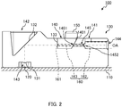
- FIG. 2 is a sectional view illustrating a configuration of optical module 100 according to the embodiment of the present invention.
- the hatching of the cross-section of optical receptacle 130 is omitted to illustrate the light paths of optical receptacle 130.
- the dashed line indicates optical axis OA.
- FIG. 2 illustrates a cross section of optical receptacle 130 taken along line A-A of FIG. 3C .
- optical module 100 includes substrate 110, photoelectric conversion element 120, and optical receptacle 130.
- Optical module 100 is used with optical transmission member 160 and optical receptacle 130 connected with each other.
- substrate 110 On substrate 110, one or more photoelectric conversion elements 120, and optical receptacle 130 are disposed. A protrusion (not illustrated in the drawing) corresponding to positioning recess 146 of optical receptacle 130 described later is formed on substrate 110. Optical receptacle 130 can be fixed at a predetermined position with respect to photoelectric conversion element 120 disposed on substrate 110 by fitting the protrusion into positioning recess 146.
- the material of substrate 110 is not limited.
- Substrate 110 is, for example, a glass composite substrate, a glass epoxy substrate or the like.
- Photoelectric conversion element 120 is a light-emitting element or a light-receiving element, and is disposed on substrate 110.
- six light-emitting elements and six light-receiving elements are disposed on substrate 110.
- six light-emitting elements (near side) and six light-receiving elements (depth side) are arranged on a straight line along the depth direction of FIG. 2 .
- the light-emitting elements are used as photoelectric conversion element 120.
- the light-receiving elements are used as photoelectric conversion element 120.
- Each light-emitting element is a vertical cavity surface emitting laser (VCSEL), for example.
- VCSEL vertical cavity surface emitting laser
- Each light-receiving element is a photodiode (PD), for example.
- Optical receptacle 130 is disposed on substrate 110 such that one or more first optical surfaces 131 described later face one or more photoelectric conversion elements 120.
- Optical receptacle 130 optically couples photoelectric conversion element 120 and end surface 161 of optical transmission member 160 in the state where optical receptacle 130 is disposed between photoelectric conversion element 120 and optical transmission member 160.
- optical receptacle 130 emits, toward end surface 161 of optical transmission member 160, light emitted from photoelectric conversion element 120 (light-emitting element).
- optical receptacle 130 In a portion that functions as optical module 100 for reception use, optical receptacle 130 emits, toward photoelectric conversion element 120 (light-receiving element), light emitted from end surface 161 of optical transmission member 160.
- Optical module 100 according to the present embodiment is an optical module for reception and transmission uses. The configurations of optical receptacle 130 are elaborated later.
- optical transmission member 160 is not limited. Optical transmission member 160 is inserted to insertion hole 145 described later. Examples of optical transmission member 160 include an optical fiber, a light waveguide, and the like. Optical transmission member 160 is connected to optical receptacle 130. In the present embodiment, optical transmission member 160 is an optical fiber. In addition, the optical fiber may be of a single mode type, or a multiple mode type.
- Optical transmission member 160 includes multicore part 162 and single core part 163.
- Multicore part 162 is, for example, a tape core wire of optical fibers, and is composed of a plurality of optical fibers collected with a tape coating.
- Single core part 163 is formed by separating multicore part 162 into single cores for example.
- Single core part 163 is disposed in insertion hole 145 and first recess 140 of optical receptacle 130 described later.
- Multicore part 162 is disposed in second recess 141 of optical receptacle 130.
- FIGS. 3A to 3E illustrate a configuration of optical receptacle 130 according to the present embodiment.
- FIG. 3A is a plan view of optical receptacle 130
- FIG. 3B is a bottom view of optical receptacle 130
- FIG. 3C is a front view of optical receptacle 130
- FIG. 3D is a back view of optical receptacle 130
- FIG. 3E is a left side view of optical receptacle 130.
- a structural configuration of optical receptacle 130 is described, and thereafter a functional configuration of optical receptacle 130 is described.
- optical receptacle 130 is a member having a substantially cuboid shape. As illustrated in FIG. 2 and FIGS. 3A to 3E , in the present embodiment, optical receptacle 130 includes first recess 140, second recess 141 and third recess 142 formed in the top surface of optical receptacle 130, fourth recess 143 formed in the bottom surface of optical receptacle 130, slope surface 1401 disposed at the inner side surface of first recess 140, insertion hole 145 configured for insertion of optical transmission member 160 and communicating between first recess 140 and second recess 141, through hole 144 communicating between second recess 141 and the outside, reference part 150 disposed on the surface (top surface) on the side on which first recess 140 and second recess 141 open, and fifth recess (positioning recess) 146 formed in the bottom surface of optical receptacle 130.
- First recess 140 is a recess having a substantially rectangular prism shape which is formed at a center portion of the top surface of optical receptacle 130.
- Second optical surface 133 described later is disposed at the inner side surface of first recess 140 on the back side of optical receptacle 130, and slope surface 1401 is disposed opposite to second optical surface 133 at the inner side surface of first recess 140 on the front surface side of optical receptacle 130.
- Slope surface 1401 is tilted such that the distance from second optical surface 133 increases toward the opening of first recess 140 (the top surface).
- the inclination angle of slope surface 1401 with respect to a plane perpendicular to the depth direction of first recess 140 is preferably 10 degrees to 60 degrees, more preferably, 10 degrees to 40 degrees.
- the plane perpendicular to the depth direction of first recess 140 and the bottom surface of optical receptacle 130 are parallel to each other.
- slope surface 1401 is formed at a portion of the inner side surface of first recess 140 where one opening (first opening 1451 described later) of insertion hole 145 is disposed such that slope surface 1401 can be visually recognized from the opening side of first recess 140.
- a portion of the inner side surface of first recess 140 where first opening 1451 is not formed may or may not be tilted.
- Second recess 141 is a recess having a substantially rectangular prism shape formed in a portion of the top surface on the front surface side of optical receptacle 130.
- the opening direction of second recess 141 is identical to that of first recess 140.
- First recess 140 and second recess 141 may open at the top surface of optical receptacle 130, or at the side surface of optical receptacle 130 as long as first recess 140 and second recess 141 open in the same direction.
- first recess 140 and second recess 141 may not open at the same plane.
- first recess 140 and second recess 141 open at the top surface side of optical receptacle 130 and on same plane.
- the other opening (second opening 1452 described later) of insertion hole 145 is disposed at the inner side surface of second recess 141 on the back side of optical receptacle 130.
- the inner side surface of second recess 141 may or may not be tilted with respect to the depth direction of second recess 141.
- the inner side surface of second recess 141 may be tilted at an inclination angle corresponding to the releasing taper for the injection molding with respect to the depth direction of second recess 141.
- through hole 144 is formed opposite to second opening 1452 on the central axis of insertion hole 145.
- An adhesive agent is supplied into first recess 140 and second recess 141 and cured in the state where single core part 163 of optical transmission member 160 is disposed in first recess 140 and insertion hole 145, and multicore part 162 is disposed in second recess 141. In this manner, optical transmission member 160 can be fixed to optical receptacle 130.
- the adhesive agent is a thermosetting resin or a photosetting resin for example, and the type of the adhesive agent is not limited as long as optical transmission member 160 can be fixed.
- Third recess 142 is a recess having a substantially triangular prism shape formed in a portion of the top surface on the back side of optical receptacle 130. Reflection surface 132 described later is disposed at a part of the inner surface of third recess 142.
- the inner surface facing reflection surface 132 may or may not be tilted with respect to the depth direction of third recess 142.
- the inner side surface of third recess 142 may be tilted at an inclination angle corresponding to the releasing taper for the injection molding with respect to the depth direction of third recess 142.
- Fourth recess 143 is a recess formed in the bottom surface of optical receptacle 130. First optical surface 131 described later is disposed at the bottom surface of fourth recess 143.
- Through hole 144 is formed on the front surface side of optical receptacle 130 on the central axis of insertion hole 145 in such a manner as to communicate between second recess 141 and the outside.
- Through hole 144 functions as a guide of optical transmission member 160 when connecting optical transmission member 160 to optical receptacle 130, and functions also as a holding part of optical transmission member 160 (to be more specific, multicore part 162).
- through hole 144 also function as an observing hole for measuring the position and the shape of second opening 1452 of insertion hole 145.
- the size of through hole 144 is greater than the opening of second opening 1452, for example, and is not limited as long as through hole 144 can function as an observing hole for measuring the position and the shape of second opening 1452.
- One or more through holes 144 are provided, and the number of through hole 144 is set in accordance with the number of first optical surface 131 and second optical surface 133.
- one through hole 144 is provided.
- the cross-sectional shape, the length, and the inclination angle of through hole 144 are not limited as long as the above-mentioned functions can be ensured. Examples of the cross-sectional shape of through hole 144 include a circular shape, a quadrangular shape and a polygonal shape. In the present embodiment, through hole 144 has a circular shape.
- Insertion hole 145 is a linear through hole including first opening 1451 opening at slope surface 1401 of first recess 140, and second opening 1452 opening at the inner side surface of second recess 141. First opening 1451 and second opening 1452 are disposed at respective both ends of insertion hole 145. As described above, insertion hole 145 communicates between first recess 140 and second recess 141. In addition, insertion hole 145 functions as a guide of optical transmission member 160 when optical transmission member 160 is inserted to optical receptacle 130 from second recess 141 side, and also functions as the holding part of optical transmission member 160 (to be more specific, single core part 163).
- Two or more insertion holes 145 are provided, and the number of insertion holes 145 is set in accordance with the numbers of first optical surface 131 and second optical surface 133.
- twelve insertion holes 145 are provided.
- the cross-sectional shape, the width, the length, and the inclination angle of insertion hole 145 are not limited as long as the above-mentioned function can be ensured.
- the examples of the cross-sectional shape of insertion hole 145 include a circular shape, a quadrangular shape and a polygonal shape.
- insertion hole 145 has a circular shape.
- insertion hole 145 is configured such that the central axis of insertion hole 145 is perpendicular to second optical surface 133 described later.
- Reference part 150 is disposed on the surface on the side on which first recess 140 and second recess 141 open. In the present embodiment, reference part 150 is disposed on the top surface of optical receptacle 130. As elaborated later, reference part 150 serves as the reference position for measuring the position and the shape of insertion hole 145 (first opening 1451 and second opening 1452). The shape, the number, the arrangement and the size of reference part 150 are not limited as long as the above-mentioned function can be ensured. Examples of the shape of reference part 150 include a recessed shape and a protruding shape. Examples of the shape in plan view of reference part 150 include a circular shape, a quadrangular shape and a polygonal shape.
- reference part 150 is a pair of protrusions, and has a circular shape in plan view.
- the pair of protrusions are arranged parallel to the arrangement direction of insertion hole 145.
- Reference part 150 may be formed integrally with optical receptacle 130, or separated from optical receptacle 130.
- Fifth recess 146 is a positioning recess that is fitted to the protrusion formed on substrate 110 so as to appropriately position twelve first optical surfaces 131 of optical receptacle 130 with respect to respective twelve photoelectric conversion elements 120.
- the shape, the number, the arrangement, and the size of fifth recess 146 are not limited, and are set in accordance with the shape of substrate 110 and the like.
- fifth recess 146 is a recess having a substantially columnar shape.
- optical receptacle 130 includes first optical surface 131, reflection surface 132 and second optical surface 133.
- twelve first optical surfaces 131 are provided.
- First optical surface 131 is an optical surface that allows light emitted from photoelectric conversion element 120 (light-emitting element) to enter optical receptacle 130, or emits, toward photoelectric conversion element 120 (light-receiving element), light passing through the inside of optical receptacle 130 after being emitted from end surface 161 of optical transmission member 160.
- the number of first optical surface 131 is not limited. In the present embodiment, as described above, twelve first optical surfaces 131 are provided. In optical receptacle 130 according to the present embodiment, six first optical surfaces 131 on the right side in FIG. 3B are used as first optical surface 131 of transmission side, and six first optical surfaces 131 on the left side in FIG. 3B are used as first optical surface 131 of reception side.
- first optical surfaces 131 are opposite to respective twelve photoelectric conversion elements 120.
- twelve first optical surfaces 131 are disposed in a line on the bottom surface of fourth recess 143 provided on the rear side (bottom surface) of optical receptacle 130.
- the shape of first optical surface 131 is not limited.
- first optical surface 131 is a convex lens surface protruding toward photoelectric conversion element 120.
- first optical surface 131 has a circular shape.
- the central axis of first optical surface 131 is perpendicular to the light-emitting surface or the light-receiving surface of photoelectric conversion element 120 (and the surface of substrate 110).
- the central axis of first optical surface 131 coincides with optical axis OA of light emitted from photoelectric conversion element 120 (light-emitting element), or light incident on photoelectric conversion element 120 (light-receiving element).
- Reflection surface 132 is an optical surface that reflects light incident on first optical surface 131 toward second optical surface 133, or reflects light incident on second optical surface 133 toward first optical surface 131.
- Reflection surface 132 is a part of the inner surface of third recess 142.
- Reflection surface 132 is tilted such that the distance to optical transmission member 160, which is disposed on the front side, decreases from the bottom surface toward the top surface of optical receptacle 130.
- the inclination angle of reflection surface 132 is not limited. In the present embodiment, the inclination angle of reflection surface 132 is 45 degrees with respect to optical axis OA of light incident on reflection surface 132.
- the shape of reflection surface 132 is not limited. In the present embodiment, reflection surface 132 is a flat surface. Light incident on first optical surface 131 or second optical surface 133 impinges on reflection surface 132 at an incident angle greater than the critical angle.
- Second optical surface 133 is an optical surface that emits, toward end surface 161 of optical transmission member 160, light passing through the inside of optical receptacle 130 after impinging on first optical surface 131, or allows light emitted from end surface 161 of optical transmission member 160 to enter optical receptacle 130.
- Second optical surface 133 is disposed at a part of the inner side surface of first recess 140 so as to face slope surface 1401 (first opening 1451).
- End surface 161 of optical transmission member 160 is disposed opposite to second optical surface 133.
- the shape of second optical surface 133 is not limited. In the present embodiment, second optical surface 133 is parallel to the depth direction of first recess 140. Preferably, second optical surface 133 is perpendicular to optical transmission member 160.
- second optical surface 133 is perpendicular to optical axis OA of light emitted from end surface 161 of optical transmission member 160, or light incident on end surface 161 of optical transmission member 160.
- Optical receptacle 130 is formed of a material that is transparent to light of a wavelength used in optical communications.
- Examples of the material of optical receptacle 130 include transparent resins such as polyetherimide (PEI) and cyclic olefin resin.
- Optical receptacle 130 is manufactured by injection molding, for example.
- light emitted from photoelectric conversion element 120 enters optical receptacle 130 from first optical surface 131.
- the incident light is converted to collimate light by first optical surface 131, and advances toward reflection surface 132.
- the incident light is reflected by reflection surface 132, and advances toward second optical surface 133.
- the light having reached second optical surface 133 is emitted out of optical receptacle 130 from second optical surface 133, and reaches end surface 161 of optical transmission member 160.
- optical module 100 For reception use, light emitted from end surface 161 of optical transmission member 160 enters optical receptacle 130 from second optical surface 133, and advances toward reflection surface 132. Then, the incident light is reflected by reflection surface 132, and advances toward first optical surface 131. The light having reached first optical surface 131 is emitted out of optical receptacle 130 from first optical surface 131, and reaches photoelectric conversion element 120 (light-receiving element). At this time, the emission light reaches the center of the light-receiving surface of photoelectric conversion element 120 (light-receiving element) while being condensed by first optical surface 131.
- optical receptacle 130 can optically couple photoelectric conversion element 120 and the end surface of optical transmission member 160 in an appropriate manner.
- a method of measuring the position and the shape of insertion hole 145 of optical receptacle 130 according to the present embodiment with a laser probe in a noncontact manner (a measurement method according to the present embodiment) is described.
- a non-contact three-dimensional measuring device using a publicly known laser probe can be used.
- a method of measuring the width (in the present embodiment, the diameter) and the inclination angle of insertion hole 145 based on the measured position and shape of insertion hole 145 are also described.
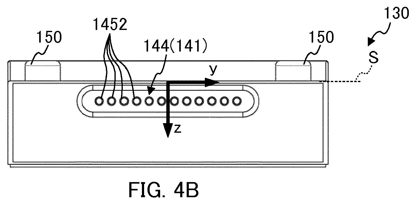
- FIGS. 4A to 4C illustrate a method of measuring the position and the shape of insertion hole 145 in optical receptacle 130.
- FIG. 4A is a sectional view of optical receptacle 130
- FIG. 4B is a front view of optical receptacle 130
- FIG. 4C is a plan view of optical receptacle 130.
- FIG. 4A is a sectional view taken along line A-A of FIG. 3C , in which hatching of optical receptacle 130 is omitted.
- FIGS. 4A is a sectional view taken along line A-A of FIG. 3C , in which hatching of optical receptacle 130 is omitted.
- the x-axis direction is the direction from the front side to the back side of optical receptacle 130
- the y-axis direction is the direction from the left side to the right side of optical receptacle 130
- the z-axis direction is the direction from the top side to the bottom side.
- the x-axis direction is parallel to the central axis of insertion hole 145
- the y-axis direction is parallel to the arrangement direction of insertion hole 145
- the z-axis direction is parallel to the depth direction of first recess 140 and second recess 141.
- a y-z plane including second opening 1452 is set as a reference (0, y, z) in the x-axis direction
- a z-x plane including the center of optical receptacle 130 in the arrangement direction (the y-axis direction) of insertion hole 145 is set as a reference (x, 0, z) in the y-axis direction
- an x-y plane of optical receptacle 130 on which reference part 150 is disposed hereinafter referred to as "reference surface S" is set as a reference (x, y, 0) in the z-axis direction.
- i represents the positions of insertion holes 145 in the arrangement direction of insertion hole 145, which are numbered from the left side as viewed from the front side of optical receptacle 130. It is to be noted that, in FIG. 4A , the white large arrow indicates the measurement direction in the steps.
- FIG. 5 is a flowchart of an exemplary measurement method according to the present embodiment.
- the measurement method according to the present embodiment includes a step of preparing optical receptacle 130 according to the present embodiment (S10), a step of measuring position A2 and the shape of second opening 1452 of insertion hole 145 through via hole 144 (S20), a step of measuring inclination angle ⁇ of slope surface 1401 from reference surface S side (S30), a step of measuring position A1 and the shape of first opening 1451 of insertion hole 145 from reference surface S side (S40), and a step of calculating the diameter and the inclination angle of insertion hole 145 (S50).
- optical receptacle 130 according to the present embodiment is prepared, and installed in the measurement device (step S10).
- position A2 (x i , y i , z i ) and the shape of second opening 1452 of insertion hole 145 are measured (step S20).
- the position (y i and z i ) and the shape of second opening 1452 in the y-axis direction and the z-axis direction are measured via through hole 144 based on the positional relationship between second opening 1452, and reference surface S and reference part 150 (see FIG. 4A ).
- Position (x i ) of second opening 1452 in the x-axis direction is defined based on the positional relationship between second opening 1452 and reference part 150 on reference surface S.
- the surface including second opening 1452 is set as the reference in the x-axis direction, and therefore xi is defined as 0.
- xi is defined as 0.
- the number of measurement points is preferably 600 or greater.
- inclination angle ⁇ of slope surface 1401 is measured (step S30).
- the inclination angle of the bottom surface (installation plane) of optical receptacle 130 and the inclination angle of slope surface 1401 with respect to reference surface (0 degrees) in the device are measured from reference surface S side (see FIG. 4A ) with a measurement device, and the difference therebetween is calculated to measure inclination angle ⁇ of slope surface 1401 with respect to the plane perpendicular to the depth direction of the first recess.
- position A1 (x i , y i , z i ) and the shape of first opening 1451 of insertion hole 145 are measured (step S40).
- position A1 and the shape of first opening 1451 of insertion hole 145 are measured from reference surface S side based on the positional relationship between first opening 1451 and reference part 150, and inclination angle ⁇ of slope surface 1401 (see FIG. 4A ).
- the position (x i and y i ) and the shape in the plane direction (the x-axis direction and the y-axis direction) of reference surface S are measured from reference surface S side based on the positional relationship between first opening 1451 and reference part 150.
- slope surface 1401 is formed at a portion of the inner side surface of first recess 140 where first opening 1451 is disposed, the position (z i ) of first opening 1451 in the z-axis direction can be calculated based on the position (x i and y i ) and the shape of first opening 1451 in the plane direction of reference surface S and inclination angle ⁇ of slope surface 1401, and as a result, position A1 and the shape of first opening 1451 can be measured.
- inclination angle ⁇ of slope surface 1401 with respect to the plane perpendicular to the depth direction of first recess 140 (the z-axis direction) is preferably 10 degrees to 60 degrees and more preferably, 10 degrees to 40 degrees.
- the number of the measurement points is preferably 600 or greater.
- the positions (position A1 of first opening 1451 and position A2 of second opening 1452) and the shape of linear insertion hole 145 can be measured.
- the positional accuracy of insertion hole 145 can be confirmed.
- the diameter and the inclination angle of insertion hole 145 are calculated (step S50).
- the diameter of insertion hole 145 and the inclination angle of insertion hole 145 are calculated based on position A1 (x i , y i , z i ) and the shape of first opening 1451 of insertion hole 145 and position A2 (x i , y i , z i ) and the shape of second opening 1452 measured at step S20 and step S40.
- slope surface 1401 is formed at a portion of the inner side surface of first recess 140 where first opening 1451 of insertion hole 145 is disposed.
- first recess 140 and second recess 141 opening in the same direction, the positions and the shapes of first opening 1451 and second opening 1452 can be measured based on the positional relationship with common reference part 150, and accordingly the position and the shape of insertion hole 145 (first opening 1451 and second opening 1452) can be correctly measured.
- position A1 and the shape of first opening 1451 are measured after position A2 and the shape of second opening 1452 are measured in the present embodiment
- the present invention is not limited to the measurement of this order.
- position A2 and the shape of second opening 1452 may be measured after position A1 and the shape of first opening 1451 are measured.
- optical receptacle 130 includes reflection surface 132
- reflection surface 132 may not be provided.
- the first optical surface and the second optical surface are disposed on the opposite sides in the optical receptacle. Then, at the portion that functions as the optical module for transmission use, light emitted from the photoelectric conversion element (light-emitting element) enters the optical receptacle from the first optical surface. The incident light reaches the second optical surface without being reflected by reflection surface 132, and is then emitted out of the optical receptacle from the second optical surface. Finally, the emission light reaches the end surface of the optical transmission member.
- first optical surfaces 131 and two or more insertion holes 145 are provided in optical receptacle 130 according to the embodiment, the present invention is not limited to this.
- one first optical surface and one insertion hole may be provided.
- one photoelectric conversion element, and one optical transmission member are used in the optical module.
- optical receptacle and the optical module according to the embodiment of the present invention are suitable for optical communications using an optical transmission member.
Landscapes
- Physics & Mathematics (AREA)
- General Physics & Mathematics (AREA)
- Optics & Photonics (AREA)
- Condensed Matter Physics & Semiconductors (AREA)
- Electromagnetism (AREA)
- Optical Couplings Of Light Guides (AREA)
- Semiconductor Lasers (AREA)
- Light Receiving Elements (AREA)
Abstract

Description
- The present invention relates to an optical receptacle including an insertion hole for inserting an optical transmission member, and an optical module including the optical receptacle, and a method of measuring the position and the shape of the insertion hole in the optical receptacle.
- Conventionally, in optical communications using an optical transmission member such as an optical fiber and an optical waveguide, an optical module including a light emitting element such as a surface-emitting laser (for example, a vertical cavity surface emitting laser (VCSEL)) has been used. The optical module includes one or more photoelectric conversion elements (light-emitting element or light-receiving element), and a light coupling element for transmission or reception (hereinafter referred to as "optical receptacle"). An optical receptacle in which a structure for holding an optical transmission member is formed is known (see, for example, PTL 1).
-
FIG. 1 is a sectional view illustrating a configuration ofoptical module 10 disclosed in PTL 1.Optical module 10 disclosed in PTL 1 includessubstrate 20,photoelectric conversion element 30 installed onsubstrate 20, andoptical receptacle 40 formed of a transparent material.Optical receptacle 40 includes firstoptical surface 41;reflection surface 42; secondoptical surface 43;first recess 44 andsecond recess 45 that open at the top surface ofoptical receptacle 40;first insertion hole 46 configured for insertion ofoptical transmission member 50 fromsecond recess 45 side and having both ends respectively open tofirst recess 44 andsecond recess 45; andsecond insertion hole 47 communicating betweensecond recess 45 and outside and configured for insertion ofoptical transmission member 50 from the outside. In the following, the opening offirst insertion hole 46 opening at the inner side surface offirst recess 44 is also referred to as "first opening 461," and the opening offirst insertion hole 46 opening at the inner side surface ofsecond recess 45 is also referred to as "second opening 462." - First
optical surface 41 allows incidence of light emitted fromphotoelectric conversion element 30.Reflection surface 42 reflects, toward secondoptical surface 43, light incident on firstoptical surface 41. Secondoptical surface 43 emits, toward the end surface ofoptical transmission member 50, light passing through the inside ofoptical receptacle 40 after enteringoptical receptacle 40 from firstoptical surface 41. Inoptical module 10 disclosed in PTL 1,optical transmission member 50 is inserted from the outside throughsecond insertion hole 47,second recess 45 andfirst insertion hole 46 in this order, and is thus connected tooptical receptacle 40. At this time,first insertion hole 46 functions as the guide ofoptical transmission member 50, andoptical transmission member 50 is connected tooptical receptacle 40 such thatend surface 51 ofoptical transmission member 50 makes contact with secondoptical surface 43. In this manner, light emitted fromphotoelectric conversion element 30 is optically coupled toend surface 51 ofoptical transmission member 50 through firstoptical surface 41,reflection surface 42 and secondoptical surface 43. - PTL 1 Japanese Patent Application Laid-Open No.
2013-235243 - In view of optically coupling
photoelectric conversion element 30 andend surface 51 ofoptical transmission member 50 in an appropriate manner by use ofoptical receptacle 10 disclosed in PTL 1, the positional accuracy offirst insertion hole 46 is an important point. The position and the shape offirst insertion hole 46 can be measured with a non-contact three-dimensional measurement device using a publicly known laser probe, for example. Inoptical receptacle 10 disclosed in PTL 1,second insertion hole 47 larger thanfirst insertion hole 46 is formed at a position opposite tosecond opening 462 offirst insertion hole 46. With this configuration, the position and the shape ofsecond opening 462 can be correctly measured throughsecond insertion hole 47 with a laser probe. On the other hand, secondoptical surface 43 is disposed at a position opposite to first opening 461 offirst insertion hole 46. Accordingly, the laser probe cannot be installed a position opposite to first opening 461, and the position and the shape offirst opening 461 cannot be correctly measured with the laser probe. Further, sincefirst opening 461 is disposed at a surface parallel to the depth direction offirst recess 44, it cannot be correctly measured also from the opening side of first opening 461 (the top surface side of optical receptacle 40) with the laser probe. - An object of the present invention is to provide an optical receptacle which can correctly measure the position and the shape of an insertion hole for inserting an optical transmission member even when an optical surface is disposed on the central axis of the insertion hole at a position opposite to one opening of the insertion hole . In addition, another object of the present invention is to provide an optical module including the above-mentioned optical receptacle. Further, another object of the present invention is to provide a method of measuring the position and the shape of an insertion hole for inserting an optical transmission member in an optical receptacle.
- An optical receptacle according to an embodiment of the present invention is configured to be disposed between a photoelectric conversion element and an optical transmission member, and to optically couple the photoelectric conversion element and an end surface of the optical transmission member, the optical receptacle including: a first optical surface configured to allow incidence of light emitted from the photoelectric conversion element, or to emit, toward the photoelectric conversion element, light emitted from the end surface of the optical transmission member and passing through inside of the optical receptacle; a second optical surface configured to emit, toward the end surface of the optical transmission member, light incident on the first optical surface that passes through the inside of the optical receptacle, or to allow incidence of light emitted from the end surface of the optical transmission member; a first recess in which the second optical surface is disposed in a part of an inner side surface of the first recess; a second recess opening in a direction identical to a direction in which the first recess opens; a slope surface disposed opposite to the second optical surface in the inner side surface of the first recess, the slope surface being tilted such that a distance of the slope surface from the second optical surface increases toward an opening of the first recess; an insertion hole having a linear shape and including a first opening and a second opening disposed at respective ends of the insertion hole; a through hole formed opposite to the second opening on a central axis of the insertion hole and communicating between the second recess and outside of the optical receptacle; and a reference part disposed on a surface of the optical receptacle on a side on which the first recess and the second recess open. The first opening opens at the slope surface of the first recess, the second opening opens at an inner side surface of the second recess, and the insertion hole is configured for insertion of the optical transmission member from the second recess side.
- An optical module according to an embodiment of the present invention includes: a substrate; a photoelectric conversion element disposed on the substrate; and the above-mentioned optical receptacle in which the first optical surfaces is disposed opposite to the photoelectric conversion element on the substrate.
- A measurement method according to an embodiment of the present invention includes is a method of measuring a position and a shape of the insertion hole in the above-mentioned optical receptacle with a laser probe in a noncontact manner, the method including: preparing the optical receptacle according to the present invention; measuring a position and a shape of the second opening via the through hole based on a positional relationship between the second opening, and a reference surface and the reference part, measuring, from the reference surface side, an inclination angle of the slope surface; and measuring, from the reference surface side, a position and a shape of the first opening based on a positional relationship between the first opening on the slope surface and the reference part, and the inclination angle of the slope surface.
- According to the present invention, the position and the shape of an insertion hole for inserting an optical transmission member in an optical receptacle can be correctly measured. In addition, according to the present invention, the width and the inclination angle of the insertion hole can be correctly measured based on the measured position and shape of the insertion hole. Accordingly, the photoelectric conversion element and the end surface of the optical transmission member can be optically coupled with each other in an appropriate manner.
-
-
FIG. 1 illustrates a configuration of the optical receptacle disclosed in PTL 1; -
FIG. 2 is a sectional view illustrating a configuration of an optical module according to an embodiment of the present invention; -
FIGS. 3A to 3E illustrate a configuration of an optical receptacle according to the embodiment of the present invention; -
FIGS. 4A to 4C illustrate a method of measuring the position and the shape of an insertion hole of the optical receptacle according to the embodiment of the present invention; and -
FIG. 5 is a flowchart of an exemplary measurement method according to the embodiment of the present invention. - An embodiment of the present invention is elaborated below with reference to the drawings.
-
FIG. 2 is a sectional view illustrating a configuration ofoptical module 100 according to the embodiment of the present invention. InFIG. 2 , the hatching of the cross-section ofoptical receptacle 130 is omitted to illustrate the light paths ofoptical receptacle 130. It is to be noted that, inFIG. 2 , the dashed line indicates optical axis OA. It is to be noted thatFIG. 2 illustrates a cross section ofoptical receptacle 130 taken along line A-A ofFIG. 3C . - As illustrated in
FIG. 2 ,optical module 100 includessubstrate 110,photoelectric conversion element 120, andoptical receptacle 130.Optical module 100 is used with optical transmission member 160 andoptical receptacle 130 connected with each other. - On
substrate 110, one or morephotoelectric conversion elements 120, andoptical receptacle 130 are disposed. A protrusion (not illustrated in the drawing) corresponding topositioning recess 146 ofoptical receptacle 130 described later is formed onsubstrate 110.Optical receptacle 130 can be fixed at a predetermined position with respect tophotoelectric conversion element 120 disposed onsubstrate 110 by fitting the protrusion intopositioning recess 146. The material ofsubstrate 110 is not limited.Substrate 110 is, for example, a glass composite substrate, a glass epoxy substrate or the like. -
Photoelectric conversion element 120 is a light-emitting element or a light-receiving element, and is disposed onsubstrate 110. In the present embodiment, six light-emitting elements and six light-receiving elements are disposed onsubstrate 110. In the present embodiment, six light-emitting elements (near side) and six light-receiving elements (depth side) are arranged on a straight line along the depth direction ofFIG. 2 . In a portion that functions asoptical module 100 for transmission use, the light-emitting elements are used asphotoelectric conversion element 120. In a portion that functions asoptical module 100 for reception use, the light-receiving elements are used asphotoelectric conversion element 120. Each light-emitting element is a vertical cavity surface emitting laser (VCSEL), for example. Each light-receiving element is a photodiode (PD), for example. -
Optical receptacle 130 is disposed onsubstrate 110 such that one or more firstoptical surfaces 131 described later face one or morephotoelectric conversion elements 120.Optical receptacle 130 optically couplesphotoelectric conversion element 120 andend surface 161 of optical transmission member 160 in the state whereoptical receptacle 130 is disposed betweenphotoelectric conversion element 120 and optical transmission member 160. In a portion that functions asoptical module 100 for transmission use,optical receptacle 130 emits, towardend surface 161 of optical transmission member 160, light emitted from photoelectric conversion element 120 (light-emitting element). In a portion that functions asoptical module 100 for reception use,optical receptacle 130 emits, toward photoelectric conversion element 120 (light-receiving element), light emitted fromend surface 161 of optical transmission member 160.Optical module 100 according to the present embodiment is an optical module for reception and transmission uses. The configurations ofoptical receptacle 130 are elaborated later. - The type of optical transmission member 160 is not limited. Optical transmission member 160 is inserted to
insertion hole 145 described later. Examples of optical transmission member 160 include an optical fiber, a light waveguide, and the like. Optical transmission member 160 is connected tooptical receptacle 130. In the present embodiment, optical transmission member 160 is an optical fiber. In addition, the optical fiber may be of a single mode type, or a multiple mode type. - Optical transmission member 160 includes multicore part 162 and single core part 163. Multicore part 162 is, for example, a tape core wire of optical fibers, and is composed of a plurality of optical fibers collected with a tape coating. Single core part 163 is formed by separating multicore part 162 into single cores for example. Single core part 163 is disposed in
insertion hole 145 andfirst recess 140 ofoptical receptacle 130 described later. Multicore part 162 is disposed insecond recess 141 ofoptical receptacle 130. -
FIGS. 3A to 3E illustrate a configuration ofoptical receptacle 130 according to the present embodiment.FIG. 3A is a plan view ofoptical receptacle 130,FIG. 3B is a bottom view ofoptical receptacle 130,FIG. 3C is a front view ofoptical receptacle 130,FIG. 3D is a back view ofoptical receptacle 130, andFIG. 3E is a left side view ofoptical receptacle 130. In the following, a structural configuration ofoptical receptacle 130 is described, and thereafter a functional configuration ofoptical receptacle 130 is described. -
Optical receptacle 130 is a member having a substantially cuboid shape. As illustrated inFIG. 2 andFIGS. 3A to 3E , in the present embodiment,optical receptacle 130 includesfirst recess 140,second recess 141 andthird recess 142 formed in the top surface ofoptical receptacle 130,fourth recess 143 formed in the bottom surface ofoptical receptacle 130,slope surface 1401 disposed at the inner side surface offirst recess 140,insertion hole 145 configured for insertion of optical transmission member 160 and communicating betweenfirst recess 140 andsecond recess 141, throughhole 144 communicating betweensecond recess 141 and the outside,reference part 150 disposed on the surface (top surface) on the side on whichfirst recess 140 andsecond recess 141 open, and fifth recess (positioning recess) 146 formed in the bottom surface ofoptical receptacle 130. In the present embodiment, throughhole 144,second recess 141,insertion hole 145 andfirst recess 140 are communicated with each other in this order from the front surface side ofoptical receptacle 130. -
First recess 140 is a recess having a substantially rectangular prism shape which is formed at a center portion of the top surface ofoptical receptacle 130. Secondoptical surface 133 described later is disposed at the inner side surface offirst recess 140 on the back side ofoptical receptacle 130, andslope surface 1401 is disposed opposite to secondoptical surface 133 at the inner side surface offirst recess 140 on the front surface side ofoptical receptacle 130.Slope surface 1401 is tilted such that the distance from secondoptical surface 133 increases toward the opening of first recess 140 (the top surface). As elaborated later, the inclination angle ofslope surface 1401 with respect to a plane perpendicular to the depth direction offirst recess 140 is preferably 10 degrees to 60 degrees, more preferably, 10 degrees to 40 degrees. In the present embodiment, the plane perpendicular to the depth direction offirst recess 140 and the bottom surface ofoptical receptacle 130 are parallel to each other. It suffices thatslope surface 1401 is formed at a portion of the inner side surface offirst recess 140 where one opening (first opening 1451 described later) ofinsertion hole 145 is disposed such thatslope surface 1401 can be visually recognized from the opening side offirst recess 140. A portion of the inner side surface offirst recess 140 wherefirst opening 1451 is not formed may or may not be tilted. -
Second recess 141 is a recess having a substantially rectangular prism shape formed in a portion of the top surface on the front surface side ofoptical receptacle 130. The opening direction ofsecond recess 141 is identical to that offirst recess 140.First recess 140 andsecond recess 141 may open at the top surface ofoptical receptacle 130, or at the side surface ofoptical receptacle 130 as long asfirst recess 140 andsecond recess 141 open in the same direction. In addition,first recess 140 andsecond recess 141 may not open at the same plane. In the present embodiment,first recess 140 andsecond recess 141 open at the top surface side ofoptical receptacle 130 and on same plane. The other opening (second opening 1452 described later) ofinsertion hole 145 is disposed at the inner side surface ofsecond recess 141 on the back side ofoptical receptacle 130. The inner side surface ofsecond recess 141 may or may not be tilted with respect to the depth direction ofsecond recess 141. For example, the inner side surface ofsecond recess 141 may be tilted at an inclination angle corresponding to the releasing taper for the injection molding with respect to the depth direction ofsecond recess 141. In addition, at the inner side surface ofsecond recess 141 on the front surface side ofoptical receptacle 130, throughhole 144 is formed opposite tosecond opening 1452 on the central axis ofinsertion hole 145. - An adhesive agent is supplied into
first recess 140 andsecond recess 141 and cured in the state where single core part 163 of optical transmission member 160 is disposed infirst recess 140 andinsertion hole 145, and multicore part 162 is disposed insecond recess 141. In this manner, optical transmission member 160 can be fixed tooptical receptacle 130. The adhesive agent is a thermosetting resin or a photosetting resin for example, and the type of the adhesive agent is not limited as long as optical transmission member 160 can be fixed. -
Third recess 142 is a recess having a substantially triangular prism shape formed in a portion of the top surface on the back side ofoptical receptacle 130.Reflection surface 132 described later is disposed at a part of the inner surface ofthird recess 142. Inthird recess 142, the inner surface facingreflection surface 132 may or may not be tilted with respect to the depth direction ofthird recess 142. For example, the inner side surface ofthird recess 142 may be tilted at an inclination angle corresponding to the releasing taper for the injection molding with respect to the depth direction ofthird recess 142. -
Fourth recess 143 is a recess formed in the bottom surface ofoptical receptacle 130. Firstoptical surface 131 described later is disposed at the bottom surface offourth recess 143. - Through
hole 144 is formed on the front surface side ofoptical receptacle 130 on the central axis ofinsertion hole 145 in such a manner as to communicate betweensecond recess 141 and the outside. Throughhole 144 functions as a guide of optical transmission member 160 when connecting optical transmission member 160 tooptical receptacle 130, and functions also as a holding part of optical transmission member 160 (to be more specific, multicore part 162). Further, throughhole 144 also function as an observing hole for measuring the position and the shape ofsecond opening 1452 ofinsertion hole 145. The size of throughhole 144 is greater than the opening ofsecond opening 1452, for example, and is not limited as long as throughhole 144 can function as an observing hole for measuring the position and the shape ofsecond opening 1452. One or more throughholes 144 are provided, and the number of throughhole 144 is set in accordance with the number of firstoptical surface 131 and secondoptical surface 133. In the present embodiment, one throughhole 144 is provided. The cross-sectional shape, the length, and the inclination angle of throughhole 144 are not limited as long as the above-mentioned functions can be ensured. Examples of the cross-sectional shape of throughhole 144 include a circular shape, a quadrangular shape and a polygonal shape. In the present embodiment, throughhole 144 has a circular shape. -
Insertion hole 145 is a linear through hole includingfirst opening 1451 opening atslope surface 1401 offirst recess 140, andsecond opening 1452 opening at the inner side surface ofsecond recess 141.First opening 1451 andsecond opening 1452 are disposed at respective both ends ofinsertion hole 145. As described above,insertion hole 145 communicates betweenfirst recess 140 andsecond recess 141. In addition,insertion hole 145 functions as a guide of optical transmission member 160 when optical transmission member 160 is inserted tooptical receptacle 130 fromsecond recess 141 side, and also functions as the holding part of optical transmission member 160 (to be more specific, single core part 163). Two ormore insertion holes 145 are provided, and the number of insertion holes 145 is set in accordance with the numbers of firstoptical surface 131 and secondoptical surface 133. In the present embodiment, twelveinsertion holes 145 are provided. The cross-sectional shape, the width, the length, and the inclination angle ofinsertion hole 145 are not limited as long as the above-mentioned function can be ensured. The examples of the cross-sectional shape ofinsertion hole 145 include a circular shape, a quadrangular shape and a polygonal shape. In the present embodiment,insertion hole 145 has a circular shape. Preferably,insertion hole 145 is configured such that the central axis ofinsertion hole 145 is perpendicular to secondoptical surface 133 described later. -
Reference part 150 is disposed on the surface on the side on whichfirst recess 140 andsecond recess 141 open. In the present embodiment,reference part 150 is disposed on the top surface ofoptical receptacle 130. As elaborated later,reference part 150 serves as the reference position for measuring the position and the shape of insertion hole 145 (first opening 1451 and second opening 1452). The shape, the number, the arrangement and the size ofreference part 150 are not limited as long as the above-mentioned function can be ensured. Examples of the shape ofreference part 150 include a recessed shape and a protruding shape. Examples of the shape in plan view ofreference part 150 include a circular shape, a quadrangular shape and a polygonal shape. In the present embodiment,reference part 150 is a pair of protrusions, and has a circular shape in plan view. In addition, in the present embodiment, the pair of protrusions are arranged parallel to the arrangement direction ofinsertion hole 145.Reference part 150 may be formed integrally withoptical receptacle 130, or separated fromoptical receptacle 130. -
Fifth recess 146 is a positioning recess that is fitted to the protrusion formed onsubstrate 110 so as to appropriately position twelve firstoptical surfaces 131 ofoptical receptacle 130 with respect to respective twelvephotoelectric conversion elements 120. The shape, the number, the arrangement, and the size offifth recess 146 are not limited, and are set in accordance with the shape ofsubstrate 110 and the like. In the present embodiment,fifth recess 146 is a recess having a substantially columnar shape. - In addition,
optical receptacle 130 includes firstoptical surface 131,reflection surface 132 and secondoptical surface 133. In the present embodiment, twelve firstoptical surfaces 131 are provided. - First
optical surface 131 is an optical surface that allows light emitted from photoelectric conversion element 120 (light-emitting element) to enteroptical receptacle 130, or emits, toward photoelectric conversion element 120 (light-receiving element), light passing through the inside ofoptical receptacle 130 after being emitted fromend surface 161 of optical transmission member 160. The number of firstoptical surface 131 is not limited. In the present embodiment, as described above, twelve firstoptical surfaces 131 are provided. Inoptical receptacle 130 according to the present embodiment, six firstoptical surfaces 131 on the right side inFIG. 3B are used as firstoptical surface 131 of transmission side, and six firstoptical surfaces 131 on the left side inFIG. 3B are used as firstoptical surface 131 of reception side. On the bottom surface ofoptical receptacle 130, twelve firstoptical surfaces 131 are opposite to respective twelvephotoelectric conversion elements 120. In the present embodiment, twelve firstoptical surfaces 131 are disposed in a line on the bottom surface offourth recess 143 provided on the rear side (bottom surface) ofoptical receptacle 130. The shape of firstoptical surface 131 is not limited. In the present embodiment, firstoptical surface 131 is a convex lens surface protruding towardphotoelectric conversion element 120. In addition, in plan view, firstoptical surface 131 has a circular shape. Preferably, the central axis of firstoptical surface 131 is perpendicular to the light-emitting surface or the light-receiving surface of photoelectric conversion element 120 (and the surface of substrate 110). In addition, preferably, the central axis of firstoptical surface 131 coincides with optical axis OA of light emitted from photoelectric conversion element 120 (light-emitting element), or light incident on photoelectric conversion element 120 (light-receiving element). -
Reflection surface 132 is an optical surface that reflects light incident on firstoptical surface 131 toward secondoptical surface 133, or reflects light incident on secondoptical surface 133 toward firstoptical surface 131.Reflection surface 132 is a part of the inner surface ofthird recess 142.Reflection surface 132 is tilted such that the distance to optical transmission member 160, which is disposed on the front side, decreases from the bottom surface toward the top surface ofoptical receptacle 130. The inclination angle ofreflection surface 132 is not limited. In the present embodiment, the inclination angle ofreflection surface 132 is 45 degrees with respect to optical axis OA of light incident onreflection surface 132. The shape ofreflection surface 132 is not limited. In the present embodiment,reflection surface 132 is a flat surface. Light incident on firstoptical surface 131 or secondoptical surface 133 impinges onreflection surface 132 at an incident angle greater than the critical angle. - Second
optical surface 133 is an optical surface that emits, towardend surface 161 of optical transmission member 160, light passing through the inside ofoptical receptacle 130 after impinging on firstoptical surface 131, or allows light emitted fromend surface 161 of optical transmission member 160 to enteroptical receptacle 130. Secondoptical surface 133 is disposed at a part of the inner side surface offirst recess 140 so as to face slope surface 1401 (first opening 1451).End surface 161 of optical transmission member 160 is disposed opposite to secondoptical surface 133. The shape of secondoptical surface 133 is not limited. In the present embodiment, secondoptical surface 133 is parallel to the depth direction offirst recess 140. Preferably, secondoptical surface 133 is perpendicular to optical transmission member 160. In addition, preferably, secondoptical surface 133 is perpendicular to optical axis OA of light emitted fromend surface 161 of optical transmission member 160, or light incident onend surface 161 of optical transmission member 160. With this configuration, it is possible to allow light emitted fromend surface 161 of optical transmission member 160 to enteroptical receptacle 130 without refracting the light, and it is possible to emit, to the outside ofoptical receptacle 130, light incident onend surface 161 of optical transmission member 160 without refracting the light. -
Optical receptacle 130 is formed of a material that is transparent to light of a wavelength used in optical communications. Examples of the material ofoptical receptacle 130 include transparent resins such as polyetherimide (PEI) and cyclic olefin resin.Optical receptacle 130 is manufactured by injection molding, for example. - Next, light paths in
optical module 100 according to the present embodiment are described. - In a portion that functions as
optical module 100 for transmission use, light emitted from photoelectric conversion element 120 (light-emitting element) entersoptical receptacle 130 from firstoptical surface 131. At this time, the incident light is converted to collimate light by firstoptical surface 131, and advances towardreflection surface 132. Then, the incident light is reflected byreflection surface 132, and advances toward secondoptical surface 133. The light having reached secondoptical surface 133 is emitted out ofoptical receptacle 130 from secondoptical surface 133, and reachesend surface 161 of optical transmission member 160. - On the other hand, in a portion that functions as
optical module 100 for reception use, light emitted fromend surface 161 of optical transmission member 160 entersoptical receptacle 130 from secondoptical surface 133, and advances towardreflection surface 132. Then, the incident light is reflected byreflection surface 132, and advances toward firstoptical surface 131. The light having reached firstoptical surface 131 is emitted out ofoptical receptacle 130 from firstoptical surface 131, and reaches photoelectric conversion element 120 (light-receiving element). At this time, the emission light reaches the center of the light-receiving surface of photoelectric conversion element 120 (light-receiving element) while being condensed by firstoptical surface 131. - In the above-mentioned configuration,
optical receptacle 130 according to the present embodiment can optically couplephotoelectric conversion element 120 and the end surface of optical transmission member 160 in an appropriate manner. - Next, a method of measuring the position and the shape of
insertion hole 145 ofoptical receptacle 130 according to the present embodiment with a laser probe in a noncontact manner (a measurement method according to the present embodiment) is described. In the measurement method according to the present embodiment, a non-contact three-dimensional measuring device using a publicly known laser probe can be used. Further, in the present embodiment, a method of measuring the width (in the present embodiment, the diameter) and the inclination angle ofinsertion hole 145 based on the measured position and shape ofinsertion hole 145 are also described. -
FIGS. 4A to 4C illustrate a method of measuring the position and the shape ofinsertion hole 145 inoptical receptacle 130.FIG. 4A is a sectional view ofoptical receptacle 130,FIG. 4B is a front view ofoptical receptacle 130, andFIG. 4C is a plan view ofoptical receptacle 130.FIG. 4A is a sectional view taken along line A-A ofFIG. 3C , in which hatching ofoptical receptacle 130 is omitted. In the following, as illustrated inFIGS. 4A to 4C , the x-axis direction is the direction from the front side to the back side ofoptical receptacle 130, the y-axis direction is the direction from the left side to the right side ofoptical receptacle 130, and the z-axis direction is the direction from the top side to the bottom side. In the present embodiment, the x-axis direction is parallel to the central axis ofinsertion hole 145, the y-axis direction is parallel to the arrangement direction ofinsertion hole 145, and the z-axis direction is parallel to the depth direction offirst recess 140 andsecond recess 141. In addition, a y-z plane includingsecond opening 1452 is set as a reference (0, y, z) in the x-axis direction, a z-x plane including the center ofoptical receptacle 130 in the arrangement direction (the y-axis direction) ofinsertion hole 145 is set as a reference (x, 0, z) in the y-axis direction, and an x-y plane ofoptical receptacle 130 on whichreference part 150 is disposed (hereinafter referred to as "reference surface S") is set as a reference (x, y, 0) in the z-axis direction. In addition, the position offirst opening 1451 of eachinsertion hole 145 is represented by A1 (xi, yi, zi)(i=1 to 12), and the position ofsecond opening 1452 of eachinsertion hole 145 is represented by A2 (xi, yi, zi)(i=1 to 12). Here, i represents the positions ofinsertion holes 145 in the arrangement direction ofinsertion hole 145, which are numbered from the left side as viewed from the front side ofoptical receptacle 130. It is to be noted that, inFIG. 4A , the white large arrow indicates the measurement direction in the steps. -
FIG. 5 is a flowchart of an exemplary measurement method according to the present embodiment. The measurement method according to the present embodiment includes a step of preparingoptical receptacle 130 according to the present embodiment (S10), a step of measuring position A2 and the shape ofsecond opening 1452 ofinsertion hole 145 through via hole 144 (S20), a step of measuring inclination angle θ ofslope surface 1401 from reference surface S side (S30), a step of measuring position A1 and the shape offirst opening 1451 ofinsertion hole 145 from reference surface S side (S40), and a step of calculating the diameter and the inclination angle of insertion hole 145 (S50). - First,
optical receptacle 130 according to the present embodiment is prepared, and installed in the measurement device (step S10). - Next, position A2 (xi, yi, zi) and the shape of
second opening 1452 ofinsertion hole 145 are measured (step S20). To be more specific, the position (yi and zi) and the shape ofsecond opening 1452 in the y-axis direction and the z-axis direction are measured via throughhole 144 based on the positional relationship betweensecond opening 1452, and reference surface S and reference part 150 (seeFIG. 4A ). Position (xi) ofsecond opening 1452 in the x-axis direction is defined based on the positional relationship betweensecond opening 1452 andreference part 150 on reference surface S. In the present embodiment, as described above, the surface includingsecond opening 1452 is set as the reference in the x-axis direction, and therefore xi is defined as 0. At this time, sincesecond recess 141 ofoptical receptacle 130 functions as an observing hole, position (xi) ofsecond opening 1452 in the x-axis direction can be correctly determined. In addition, from the viewpoint of measuring position A2 (xi, yi, zi) and the shape ofsecond opening 1452 with high accuracy, the number of measurement points is preferably 600 or greater. - Next, inclination angle θ of
slope surface 1401 is measured (step S30). To be more specific, the inclination angle of the bottom surface (installation plane) ofoptical receptacle 130 and the inclination angle ofslope surface 1401 with respect to reference surface (0 degrees) in the device are measured from reference surface S side (seeFIG. 4A ) with a measurement device, and the difference therebetween is calculated to measure inclination angle θ ofslope surface 1401 with respect to the plane perpendicular to the depth direction of the first recess. - Next, position A1 (xi, yi, zi) and the shape of
first opening 1451 ofinsertion hole 145 are measured (step S40). To be more specific, position A1 and the shape offirst opening 1451 ofinsertion hole 145 are measured from reference surface S side based on the positional relationship betweenfirst opening 1451 andreference part 150, and inclination angle θ of slope surface 1401 (seeFIG. 4A ). To be more specific, the position (xi and yi) and the shape in the plane direction (the x-axis direction and the y-axis direction) of reference surface S are measured from reference surface S side based on the positional relationship betweenfirst opening 1451 andreference part 150. Sinceslope surface 1401 is formed at a portion of the inner side surface offirst recess 140 wherefirst opening 1451 is disposed, the position (zi) offirst opening 1451 in the z-axis direction can be calculated based on the position (xi and yi) and the shape offirst opening 1451 in the plane direction of reference surface S and inclination angle θ ofslope surface 1401, and as a result, position A1 and the shape offirst opening 1451 can be measured. In view of appropriately measuring position A1 and the shape offirst opening 1451 from reference surface S side, inclination angle θ ofslope surface 1401 with respect to the plane perpendicular to the depth direction of first recess 140 (the z-axis direction) (in the present embodiment, the bottom surface of optical receptacle 130) is preferably 10 degrees to 60 degrees and more preferably, 10 degrees to 40 degrees. In addition, in view of measuring position A1 (xi, yi, zi) and the shape offirst opening 1451 with high accuracy, the number of the measurement points is preferably 600 or greater. - Through the above-mentioned steps, the positions (position A1 of
first opening 1451 and position A2 of second opening 1452) and the shape oflinear insertion hole 145 can be measured. Thus, the positional accuracy ofinsertion hole 145 can be confirmed. - Finally, the diameter and the inclination angle of
insertion hole 145 are calculated (step S50). To be more specific, the diameter ofinsertion hole 145 and the inclination angle ofinsertion hole 145 are calculated based on position A1 (xi, yi, zi) and the shape offirst opening 1451 ofinsertion hole 145 and position A2 (xi, yi, zi) and the shape ofsecond opening 1452 measured at step S20 and step S40. - In
optical receptacle 130 according to the present embodiment,slope surface 1401 is formed at a portion of the inner side surface offirst recess 140 wherefirst opening 1451 ofinsertion hole 145 is disposed. With this configuration, the position and the shape ofinsertion hole 145 can be correctly measured from above even when secondoptical surface 133 is disposed opposite tofirst opening 1451. In addition, with the present embodiment, the diameter and the inclination angle can also be measured. In addition, in the present embodiment,second recess 141 opens at reference surface S, and thus the position ofsecond opening 1452 ofinsertion hole 145 in the x-axis direction can be correctly determined. Further, withfirst recess 140 andsecond recess 141 opening in the same direction, the positions and the shapes offirst opening 1451 andsecond opening 1452 can be measured based on the positional relationship withcommon reference part 150, and accordingly the position and the shape of insertion hole 145 (first opening 1451 and second opening 1452) can be correctly measured. - While position A1 and the shape of
first opening 1451 are measured after position A2 and the shape ofsecond opening 1452 are measured in the present embodiment, the present invention is not limited to the measurement of this order. For example, position A2 and the shape ofsecond opening 1452 may be measured after position A1 and the shape offirst opening 1451 are measured. - In addition, while
optical receptacle 130 according to the embodiment includesreflection surface 132,reflection surface 132 may not be provided. In this case, the first optical surface and the second optical surface are disposed on the opposite sides in the optical receptacle. Then, at the portion that functions as the optical module for transmission use, light emitted from the photoelectric conversion element (light-emitting element) enters the optical receptacle from the first optical surface. The incident light reaches the second optical surface without being reflected byreflection surface 132, and is then emitted out of the optical receptacle from the second optical surface. Finally, the emission light reaches the end surface of the optical transmission member. On the other hand, in the portion that functions as the optical module for reception use, light emitted from the end surface of the optical transmission member enters the optical receptacle from the second optical surface. The incident light reaches the first optical surface, and is then emitted out of the optical receptacle from the first optical surface. Finally, the emission light reaches the photoelectric conversion element (light-receiving element). - Further, while two or more first
optical surfaces 131 and two ormore insertion holes 145 are provided inoptical receptacle 130 according to the embodiment, the present invention is not limited to this. In the present invention, one first optical surface and one insertion hole may be provided. In this case, in the optical module, one photoelectric conversion element, and one optical transmission member are used. - This application is entitled to and claims the benefit of Japanese Patent Application No.
2016-000128 filed on January 4, 2016 - The optical receptacle and the optical module according to the embodiment of the present invention are suitable for optical communications using an optical transmission member.
-
- 10 Optical module
- 20 Substrate
- 30 Photoelectric conversion element
- 40 Optical receptacle
- 41 First optical surface
- 42 Reflection surface
- 43 Second optical surface
- 44 First recess
- 45 Second recess
- 46 First insertion hole
- 461 First opening
- 462 Second opening
- 47 Second insertion hole
- 50 Optical transmission member
- 51 End surface of optical transmission member
- 100 Optical module
- 110 Substrate
- 120 Photoelectric conversion element
- 130 Optical receptacle
- 131 First optical surface
- 132 Reflection surface
- 133 Second optical surface
- 140 First recess
- 1401 Slope surface
- 141 Second recess
- 142 Third recess
- 143 Fourth recess
- 144 Through hole
- 145 Insertion hole
- 1451 First opening
- 1452 Second opening
- 146 Fifth recess
- 150 Reference part
- 160 Optical transmission member
- 161 End surface of optical transmission member
- 162 Multicore part
- 163 Single core part
- OA Optical axis
- S Reference surface
- θ Inclination angle of slope surface
Claims (8)
- An optical receptacle configured to be disposed between a photoelectric conversion element and an optical transmission member, and to optically couple the photoelectric conversion element and an end surface of the optical transmission member, the optical receptacle comprising:a first optical surface configured to allow incidence of light emitted from the photoelectric conversion element, or to emit, toward the photoelectric conversion element, light emitted from the end surface of the optical transmission member and passing through inside of the optical receptacle;a second optical surface configured to emit, toward the end surface of the optical transmission member, light incident on the first optical surface that passes through the inside of the optical receptacle, or to allow incidence of light emitted from the end surface of the optical transmission member;a first recess in which the second optical surface is disposed in a part of an inner side surface of the first recess;a second recess opening in a direction identical to a direction in which the first recess opens;a slope surface disposed opposite to the second optical surface in the inner side surface of the first recess, the slope surface being tilted such that a distance of the slope surface from the second optical surface increases toward an opening of the first recess;an insertion hole having a linear shape and including a first opening and a second opening disposed at respective ends of the insertion hole, wherein the first opening opens at the slope surface of the first recess, the second opening opens at an inner side surface of the second recess, and the insertion hole is configured for insertion of the optical transmission member from the second recess side;a through hole formed opposite to the second opening on a central axis of the insertion hole and communicating between the second recess and outside of the optical receptacle; anda reference part disposed on a surface of the optical receptacle on a side on which the first recess and the second recess open.
- The optical receptacle according to claim 1, wherein an inclination angle of the slope surface with respect to a plane perpendicular to a depth direction of the first recess is 10 degrees to 60 degrees.
- The optical receptacle according to claim 1 or 2, wherein the reference part is a pair of protrusions or a pair of recesses.
- The optical receptacle according to any one of claims 1 to 3, further comprising, a reflection surface configured to reflect light incident on the first optical surface toward the second optical surface, or to reflect light incident on the second optical surface toward the first optical surface.
- An optical module comprising:a substrate;a photoelectric conversion element disposed on the substrate; andthe optical receptacle according to any one of claims 1 to 4 in which the first optical surfaces is disposed opposite to the photoelectric conversion element on the substrate.
- A method of measuring a position and a shape of the insertion hole in the optical receptacle according to any one of claims 1 to 4 with a laser probe in a noncontact manner, the method comprising:preparing the optical receptacle according to any one of claims 1 to 4;measuring a position and a shape of the second opening via the through hole based on a positional relationship between the second opening, and a reference surface and the reference part, wherein the reference surface is the surface on which the reference part is disposed in the optical receptacle;measuring, from the reference surface side, an inclination angle of the slope surface; andmeasuring, from the reference surface side, a position and a shape of the first opening based on a positional relationship between the first opening on the slope surface and the reference part, and the inclination angle of the slope surface.
- The method according to claim 6, further comprising, calculating a width of the insertion hole based on the positions and the shapes of the first opening and the second opening.
- The method according to claim 6 or 7, further comprising, calculating an inclination angle of the insertion hole based on a positional relationship between the first opening and the second opening.
Applications Claiming Priority (2)
| Application Number | Priority Date | Filing Date | Title |
|---|---|---|---|
| JP2016000128A JP2017122754A (en) | 2016-01-04 | 2016-01-04 | Optical receptacle, optical module, and measuring method |
| PCT/JP2016/087470 WO2017119259A1 (en) | 2016-01-04 | 2016-12-16 | Optical receptacle, optical module, and measurement method |
Publications (2)
| Publication Number | Publication Date |
|---|---|
| EP3401717A1 true EP3401717A1 (en) | 2018-11-14 |
| EP3401717A4 EP3401717A4 (en) | 2019-08-14 |
Family
ID=59274306
Family Applications (1)
| Application Number | Title | Priority Date | Filing Date |
|---|---|---|---|
| EP16883759.9A Withdrawn EP3401717A4 (en) | 2016-01-04 | 2016-12-16 | OPTICAL RECEPTACLE, OPTICAL MODULE, AND MEASURING METHOD |
Country Status (5)
| Country | Link |
|---|---|
| US (1) | US10459178B2 (en) |
| EP (1) | EP3401717A4 (en) |
| JP (1) | JP2017122754A (en) |
| CN (1) | CN108474916B (en) |
| WO (1) | WO2017119259A1 (en) |
Families Citing this family (1)
| Publication number | Priority date | Publication date | Assignee | Title |
|---|---|---|---|---|
| US11552205B2 (en) * | 2020-11-13 | 2023-01-10 | Taiwan Semiconductor Manufacturing Company, Ltd. | Optical sensing device having inclined reflective surface |
Family Cites Families (21)
| Publication number | Priority date | Publication date | Assignee | Title |
|---|---|---|---|---|
| US7050678B1 (en) * | 1998-08-28 | 2006-05-23 | Fujikura Ltd. | Optical module, optical element attachment method, and receptacle-fitted optical module |
| MXPA03006104A (en) * | 2001-01-09 | 2005-10-05 | Takahiko Mukouda | Connector component for multi-core optical fiber, ferrule, and method for manufacturing the same. |
| US6619855B2 (en) * | 2001-06-29 | 2003-09-16 | Xanoptix, Inc. | Post-formation feature optimization |
| JPWO2005052666A1 (en) * | 2003-11-27 | 2008-03-06 | イビデン株式会社 | IC chip mounting substrate, motherboard substrate, optical communication device, IC chip mounting substrate manufacturing method, and motherboard substrate manufacturing method |
| JP4606954B2 (en) * | 2004-07-15 | 2011-01-05 | Toto株式会社 | Ferrule holding member for optical receptacle, method for manufacturing the same, and optical receptacle using the same |
| US7556440B2 (en) * | 2006-12-22 | 2009-07-07 | Lightwire Inc. | Dual-lensed unitary optical receiver assembly |
| JP5156502B2 (en) * | 2007-06-26 | 2013-03-06 | パナソニック株式会社 | Optical module |
| US8985865B2 (en) * | 2008-11-28 | 2015-03-24 | Us Conec, Ltd. | Unitary fiber optic ferrule and adapter therefor |
| JP2011085647A (en) * | 2009-10-13 | 2011-04-28 | Hitachi Chem Co Ltd | Optical waveguide substrate and method for manufacturing the same |
| US8961037B2 (en) * | 2009-10-16 | 2015-02-24 | Fujikura Ltd. | Optical connector |
| US9134489B2 (en) * | 2009-11-11 | 2015-09-15 | Samtec, Inc. | Optical engine for active optical cable |
| TWI524103B (en) * | 2010-12-14 | 2016-03-01 | 鴻海精密工業股份有限公司 | Optical fiber coupling connector and assembling method for same |
| TWI497142B (en) * | 2011-01-26 | 2015-08-21 | Hon Hai Prec Ind Co Ltd | Optical fiber connector |
| US9377594B2 (en) * | 2011-12-29 | 2016-06-28 | Intel Corporation | Two-dimensional, high-density optical connector |
| JP2013235243A (en) * | 2012-04-09 | 2013-11-21 | Fujikura Ltd | Optical path changing member |
| US9348102B2 (en) * | 2012-12-03 | 2016-05-24 | Finisar Corporation | Pin cadence for high-speed connectors |
| US8903210B2 (en) * | 2013-04-29 | 2014-12-02 | International Business Machines Corporation | Vertical bend waveguide coupler for photonics applications |
| US9739962B2 (en) * | 2013-05-14 | 2017-08-22 | Vixar | Plastic optical fiber data communication links |
| JP6255237B2 (en) * | 2013-12-25 | 2017-12-27 | 株式会社エンプラス | Optical receptacle and optical module |
| EP3271765A1 (en) | 2015-03-19 | 2018-01-24 | Corning Optical Communications LLC | A connector device for connecting at least one optical fiber end piece and manufacturing method |
| US9766416B1 (en) * | 2016-09-12 | 2017-09-19 | Yottahn, Inc. | Optical module and method of manufacturing the same |
-
2016
- 2016-01-04 JP JP2016000128A patent/JP2017122754A/en active Pending
- 2016-12-16 EP EP16883759.9A patent/EP3401717A4/en not_active Withdrawn
- 2016-12-16 CN CN201680077258.9A patent/CN108474916B/en not_active Expired - Fee Related
- 2016-12-16 WO PCT/JP2016/087470 patent/WO2017119259A1/en not_active Ceased
- 2016-12-16 US US16/067,827 patent/US10459178B2/en not_active Expired - Fee Related
Also Published As
| Publication number | Publication date |
|---|---|
| CN108474916B (en) | 2020-07-03 |
| US10459178B2 (en) | 2019-10-29 |
| WO2017119259A1 (en) | 2017-07-13 |
| EP3401717A4 (en) | 2019-08-14 |
| CN108474916A (en) | 2018-08-31 |
| JP2017122754A (en) | 2017-07-13 |
| US20190011651A1 (en) | 2019-01-10 |
Similar Documents
| Publication | Publication Date | Title |
|---|---|---|
| JP5238651B2 (en) | Optical path changing member, optical connection method | |
| US9158071B2 (en) | Optical path-changing member | |
| US9201201B2 (en) | Fiber trays, fiber optical modules, and methods of processing optical fibers | |
| US7614802B2 (en) | Optically coupled device and optical module including optically coupled device | |
| US20130230280A1 (en) | Modularized interposer | |
| US20190033528A1 (en) | Optical connector and optical transmission module | |
| US9588306B2 (en) | Fiber optic module assemblies and connector assemblies using the same | |
| US9244234B2 (en) | Optical receptacle and optical module | |
| US10416397B2 (en) | Optical receptacle, optical module, and method for manufacturing optical module | |
| US10451822B2 (en) | Optical module manufacturing method, optical module receptacle and optical module | |
| EP3121631A1 (en) | Optical receptacle and optical module | |
| US10156687B2 (en) | Optical receptacle and optical module | |
| US9804351B2 (en) | Optical receptacle and optical module | |
| US10627586B2 (en) | Optical receptacle, optical module, and method for manufacturing optical module | |
| US10459178B2 (en) | Optical receptacle, optical module, and measurement method | |
| JP6729060B2 (en) | Optical connector ferrule and method for measuring eccentricity of optical connector ferrule | |
| US20190101710A1 (en) | Optical receptacle and optical module | |
| EP3546998A1 (en) | Optical module and manufacturing method for optical module | |
| JPWO2016175126A1 (en) | Optical transmission module | |
| JP2016048284A (en) | Optical receptacle and optical module | |
| US20240319452A1 (en) | Optical receptacle and optical module | |
| US20220082768A1 (en) | Optical module and optical connector cable |
Legal Events
| Date | Code | Title | Description |
|---|---|---|---|
| STAA | Information on the status of an ep patent application or granted ep patent |
Free format text: STATUS: THE INTERNATIONAL PUBLICATION HAS BEEN MADE |
|
| PUAI | Public reference made under article 153(3) epc to a published international application that has entered the european phase |
Free format text: ORIGINAL CODE: 0009012 |
|
| STAA | Information on the status of an ep patent application or granted ep patent |
Free format text: STATUS: REQUEST FOR EXAMINATION WAS MADE |
|
| 17P | Request for examination filed |
Effective date: 20180629 |
|
| AK | Designated contracting states |
Kind code of ref document: A1 Designated state(s): AL AT BE BG CH CY CZ DE DK EE ES FI FR GB GR HR HU IE IS IT LI LT LU LV MC MK MT NL NO PL PT RO RS SE SI SK SM TR |
|
| AX | Request for extension of the european patent |
Extension state: BA ME |
|
| DAV | Request for validation of the european patent (deleted) | ||
| DAX | Request for extension of the european patent (deleted) | ||
| A4 | Supplementary search report drawn up and despatched |
Effective date: 20190711 |
|
| RIC1 | Information provided on ipc code assigned before grant |
Ipc: H01L 31/0232 20140101ALI20190705BHEP Ipc: H01S 5/022 20060101ALI20190705BHEP Ipc: G02B 6/42 20060101AFI20190705BHEP |
|
| STAA | Information on the status of an ep patent application or granted ep patent |
Free format text: STATUS: THE APPLICATION IS DEEMED TO BE WITHDRAWN |
|
| 18D | Application deemed to be withdrawn |
Effective date: 20220701 |