EP3401692A1 - Capacitive sensing system and related voltage correction method therefor - Google Patents
Capacitive sensing system and related voltage correction method therefor Download PDFInfo
- Publication number
- EP3401692A1 EP3401692A1 EP16922669.3A EP16922669A EP3401692A1 EP 3401692 A1 EP3401692 A1 EP 3401692A1 EP 16922669 A EP16922669 A EP 16922669A EP 3401692 A1 EP3401692 A1 EP 3401692A1
- Authority
- EP
- European Patent Office
- Prior art keywords
- data value
- unit
- pixel data
- pixel
- original pixel
- Prior art date
- Legal status (The legal status is an assumption and is not a legal conclusion. Google has not performed a legal analysis and makes no representation as to the accuracy of the status listed.)
- Withdrawn
Links
Images

Classifications
-
- G—PHYSICS
- G06—COMPUTING OR CALCULATING; COUNTING
- G06V—IMAGE OR VIDEO RECOGNITION OR UNDERSTANDING
- G06V40/00—Recognition of biometric, human-related or animal-related patterns in image or video data
- G06V40/10—Human or animal bodies, e.g. vehicle occupants or pedestrians; Body parts, e.g. hands
- G06V40/12—Fingerprints or palmprints
- G06V40/13—Sensors therefor
- G06V40/1306—Sensors therefor non-optical, e.g. ultrasonic or capacitive sensing
-
- G—PHYSICS
- G01—MEASURING; TESTING
- G01R—MEASURING ELECTRIC VARIABLES; MEASURING MAGNETIC VARIABLES
- G01R27/00—Arrangements for measuring resistance, reactance, impedance, or electric characteristics derived therefrom
- G01R27/02—Measuring real or complex resistance, reactance, impedance, or other two-pole characteristics derived therefrom, e.g. time constant
- G01R27/26—Measuring inductance or capacitance; Measuring quality factor, e.g. by using the resonance method; Measuring loss factor; Measuring dielectric constants ; Measuring impedance or related variables
Definitions
- the disclosure relates to the field of electronics, and in particular to a capacitive sensing system and a method for voltage calibration of the same.
- a main object of the present disclosure is to provide a capacitive sensing system and a method for voltage calibration of the same, in which a voltage variation of a capacitive sensing device is calibrated by a resistor so as to prevent occurrence of image distortion.
- the present disclosure provides a capacitive sensing system, including: a pixel matrix, arranged for sensing a plurality of voltage variations generated by pressing of a fingerprint; and a calibration unit, coupled to the pixel matrix, the calibration unit being used for calibrating the plurality of voltage variations of the pixel matrix according to a control signal generated based on the plurality of voltage variations.
- the capacitive sensing system further includes: an analog-to-digital converter, coupled to the pixel matrix, the analog-to-digital converter being used for converting the plurality of voltage variations into a plurality of original pixel data values; and a control unit, coupled to the analog-to-digital converter, the control unit being used for generating the control signal based on the plurality of original pixel data values.
- the pixel matrix includes a plurality of pixel units, and the plurality of pixel units correspond to the plurality of voltage variations respectively.
- the calibration unit is a variable resistor which is used for generating a calibration voltage according to the control signal so as to adjust the plurality of voltage variations.
- the control signal is determined by the control unit according to a difference between the first original pixel data value and the second original pixel data value.
- the calibration unit generates a voltage-drop current according to the control signal so as to reduce the voltage variation corresponding to the first pixel unit.
- the control signal is determined by the control unit according to the difference between the first original pixel data value and the second original pixel data value.
- the calibration unit generates the voltage-drop current according to the control signal so as to reduce the voltage variation corresponding to the second pixel unit.
- the voltage variation is maintained by the calibration unit to be less than a voltage swing range of the analog-to-digital converter according to the control signal.
- the present disclosure further provides a voltage calibration method for a pixel matrix, the method includes: determining a first original pixel data value corresponding to a first pixel unit and a second original pixel data value corresponding to a second pixel unit which is located in the same row as the first pixel unit; determining a control signal according to a difference between the first original pixel data value and the second original pixel data value; and adjusting the first original pixel data value corresponding to the first pixel unit or the second original pixel data value corresponding to the second pixel unit according to the control signal.
- the method further includes: when the first original pixel data value corresponding to the first pixel unit is greater than the second original pixel data value corresponding to the second pixel unit which is located in the same row as the first pixel unit, determining the control signal according to the difference between the first original pixel data value and the second original pixel data value; and generating a voltage-drop current according to the control signal so as to reduce the first original pixel data value corresponding to the first pixel unit.
- the method further includes: when the first original pixel data value corresponding to the first pixel unit is smaller than the second original pixel data value corresponding to the second pixel unit which is located in the same row as the first pixel unit, determining the control signal according to the difference between the first original pixel data value and the second original pixel data value; and generating a voltage-drop current according to the control signal so as to reduce the second original pixel data value corresponding to the second pixel unit.
- the capacitive sensing system according to the present disclosure has advantages of improving the consistency of voltage variations detected by pixel units and avoiding the distortion during image processing.
- FIG. 1 is a schematic diagram of a capacitive sensing system 10 according to some embodiments of the present disclosure.
- the capacitive sensing system 10 may be implemented in a form of a touch screen device, a capacitive sensing device or a fingerprint identification device so as to sense the images sensed by the touch screen device or the fingerprint identification device.
- the capacitive sensing system 10 includes: a pixel matrix 102, an analog-to-digital converter 104, a control unit 106 and a calibration unit 108.
- the pixel matrix 102 is a matrix of pixel units including n columns and m rows, and is used for sensing a plurality of voltage variations V p_nm (where n and m represent a pixel unit located in the n th column and the m th row respectively in the pixel matrix 102) corresponding to the pixel matrix 102, which are generated when a fingerprint presses on a capacitive sensing device.
- the analog-to-digital converter 104 is coupled to the pixel matrix 102, and is used for converting the plurality of voltage variations V p_nm into a plurality of original pixel data values.
- the control unit 106 is coupled to the analog-to-digital converter 104, and is used for generating a control signal based on the plurality of original pixel data values.
- the calibration unit 108 is coupled to the control unit 106, and is used for calibrating the voltage variations V p_nm of the pixel matrix 102 according to the control signal generated by the control unit 106, thus avoiding the distortion of the voltage variations V p_nm .
- a capacitance error ⁇ C s may be introduced to the capacitance sensing device due to the process offset or parasitic capacitance effect. Therefore, capacitive sensing results of the pixel units may not be completely the same to each other.
- a voltage error ⁇ V p may be introduced to the voltage variations V p_nm of the pixel units due to the capacitance error ⁇ C s , and thus the voltage variations V p_nm of the pixel unit may exceed a range of a voltage swing V swing of the analog-to-digital converter 104, which causes distortion of the output original pixel data values and erroneous determination.
- the capacitive sensing system 10 of the present disclosure when the capacitive sensing device is pressed by a fingerprint, the voltage variations V p_nm corresponding to individual pixel units are generated by the pixel matrix 102 through charging and discharging capacitors. After the voltage variations V p_nm of the individual pixel units are converted by the analog-to-digital converter 104 into original pixel data values, a control signal is generated by the control unit 106 based on the plurality of original pixel data values obtained after conversion, and is transmitted to the calibration unit 108.
- a calibration voltage V ref_nm (where n and m represent a pixel unit of the n th column and the m th row respectively in the pixel matrix 102) is generated by the calibration unit 108 according to the control signal, so as to adjust the voltage variations V p_nm of the pixel units.
- the calibration unit 108 may be a variable resistor or other devices which generate a variable impedance to change the voltage of a node where the calibration unit 108 is located, and the disclosure is not limited to this.
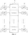
- FIG. 2 is a schematic diagram of the pixel matrix 102 and the calibration unit 108 according to some embodiments of the present disclosure. Since each of the pixel units in the same row of the pixel matrix 102 is influenced by a capacitance effect, the voltage variations of the pixel units in the same row exhibit a linearly ascending or descending trend.
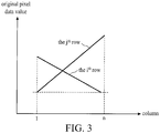
- FIG. 3 is a schematic diagram of the distribution of original pixel data values of pixel units in the same row that are not calibrated according to some embodiments of the present disclosure.
- a voltage-drop current I is generated when the variable resistor of the calibration unit 108 is turned on, so as to reduce a voltage variation V p_nm of the first pixel unit in the same row or the n th pixel unit in the same row, and to further adjust a voltage variation V p_nm of each pixel unit in the same row.
- the first pixel unit and the n th pixel unit of the pixel units in the i th row have a corresponding first original pixel data value and a corresponding n th original pixel data value, respectively. As shown in FIG.
- a line denoted as the i th row represents the distribution of the original pixel data values of the pixel units in the i th row in the pixel array 102.
- the first original pixel data value is greater than the n th original pixel data value, which means that the first original pixel unit is influenced by capacitance process offset or parasitic capacitance effect such that the first original pixel data value is greater than the n th original pixel data value.
- a control signal is generated by the control unit 106 and is transmitted to the calibration unit 108.
- a calibration voltage V ref_11 is determined by the calibration unit 108 according to a difference between the first original pixel data value and the n th original pixel data value, in order to reduce the voltage variation V p_11 corresponding to the first pixel unit.
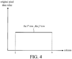
- the voltage variation V p_11 of the first original pixel data value corresponding to the first pixel unit can be reduced using the calibration voltage V ref_11 . Therefore, the first original pixel data value after calibration is consistent with the n th original pixel data value in the i th row.
- the first original pixel data value is smaller than the n th original pixel data value, that is, as shown in FIG. 3 , in which a line denoted as the j th row represents the distribution of the original pixel data values of the pixel units in the j th row in the pixel array 102
- the n th original pixel unit in the j th row is influenced by capacitance process offset or parasitic capacitance effect
- the first original pixel data value is smaller than the n th original pixel data value.
- a control signal is generated by the control unit 106 and is transmitted to the calibration unit 108.
- a calibration voltage V ref_1n can be determined by the calibration unit 108 according to a difference between the first original pixel data value and the n th original pixel data value so as to reduce the voltage variation V p_1n corresponding to the n th pixel unit.
- V p_1n the voltage variation of the n th pixel unit generated due to fingerprint pressing
- the voltage variation V p_1n of the n th original pixel data value corresponding to the n th pixel unit can be reduced using the calibration voltage V ref_1n . Therefore, the first original pixel data value is consistent with the n th original pixel data value after calibration in the j th row.
- the original pixel data values without being calibrated by the calibration unit 108 may be distorted due to the process offset or parasitic capacitance effect, and therefore the distribution of the original pixel data values exhibits no consistency (that is, the original pixel data values of individual pixel units in the same row are not completely the same).
- the consistency of the original pixel data values of the pixel units in the same row may be improved after being calibrated one by one by the calibration unit 108 so that the voltage variation V p_nm output by the pixel unit does not exceed a voltage swing range V swing of the analog-to-digital converter 104. Therefore, the original pixel data values are distributed with consistency, thus reducing the distortion situation.
- the voltage calibration can be performed by the calibration unit 108 of the present disclosure on the first pixel unit and the n th pixel unit in the same row of the pixel matrix 102 (as described in the foregoing embodiments), but also the voltage calibration can be performed by the calibration unit 108 on any two pixel units in the same row of the pixel matrix 102 (for example, the third pixel unit and the fifth pixel unit in the same row of the pixel matrix); alternatively, the voltage calibration may be performed by the calibration unit 108 on more than two pixel units in the same row of the pixel matrix 102, and the voltage calibration is further performed on all the pixel units in the pixel matrix 102 after the pixel units in the same row of the pixel matrix 102 are calibrated.
- the calibration unit 108 may adjust not only the voltage of the node where the variable resistor is located by generating the voltage-drop current I, but also adjust the voltage variations V p_nm of the pixel units by increasing the voltage of the node where the calibration unit 108 is located, and the disclosure is not limited to this. All the above described methods will fall within the scope of the present disclosure.
- the voltage variations detected by the pixel units are calibrated so as to improve the consistency of the voltage variations, thereby reducing distortions in image processing.
Landscapes
- Engineering & Computer Science (AREA)
- Physics & Mathematics (AREA)
- General Physics & Mathematics (AREA)
- Human Computer Interaction (AREA)
- Multimedia (AREA)
- Theoretical Computer Science (AREA)
- Image Input (AREA)
Abstract
Description
- The disclosure relates to the field of electronics, and in particular to a capacitive sensing system and a method for voltage calibration of the same.
- With the development and progress of science and technology, mobile electronic devices such as mobile phones, digital cameras, tablet computers, and notebook computers have become indispensable tools in people's lives. In order to effectively prevent the data inside the personal mobile electronic devices from being stolen, various protection methods have been devised accordingly, such as password verification, voiceprint identification, or fingerprint identification, wherein the fingerprint identification is widely used. In existing capacitive sensing devices, the capacitance variation generated by charging and discharging a capacitor is typically converted into original data value; however, since a distortion of the conversion voltage variation is caused by process offset or parasitic capacitance effect, errors or distortions in image processing are caused accordingly.
- Therefore, how to provide a system for sensing capacitances to avoid occurrence of the above situation becomes one of the goals to be achieved in the industry.
- Therefore, a main object of the present disclosure is to provide a capacitive sensing system and a method for voltage calibration of the same, in which a voltage variation of a capacitive sensing device is calibrated by a resistor so as to prevent occurrence of image distortion.
- In order to solve the above issues, the present disclosure provides a capacitive sensing system, including: a pixel matrix, arranged for sensing a plurality of voltage variations generated by pressing of a fingerprint; and a calibration unit, coupled to the pixel matrix, the calibration unit being used for calibrating the plurality of voltage variations of the pixel matrix according to a control signal generated based on the plurality of voltage variations.
- For instance, the capacitive sensing system further includes: an analog-to-digital converter, coupled to the pixel matrix, the analog-to-digital converter being used for converting the plurality of voltage variations into a plurality of original pixel data values; and a control unit, coupled to the analog-to-digital converter, the control unit being used for generating the control signal based on the plurality of original pixel data values.
- For instance, the pixel matrix includes a plurality of pixel units, and the plurality of pixel units correspond to the plurality of voltage variations respectively.
- For instance, the calibration unit is a variable resistor which is used for generating a calibration voltage according to the control signal so as to adjust the plurality of voltage variations.
- For instance, when a first original pixel data value corresponding to a first pixel unit is greater than a second original pixel data value corresponding to a second pixel unit which is located in the same row as the first pixel unit, the control signal is determined by the control unit according to a difference between the first original pixel data value and the second original pixel data value.
- For instance, the calibration unit generates a voltage-drop current according to the control signal so as to reduce the voltage variation corresponding to the first pixel unit.
- For instance, when the first original pixel data value corresponding to the first pixel unit is smaller than the second original pixel data value corresponding to the second pixel unit which is located in the same row as the first pixel unit, the control signal is determined by the control unit according to the difference between the first original pixel data value and the second original pixel data value.
- For instance, the calibration unit generates the voltage-drop current according to the control signal so as to reduce the voltage variation corresponding to the second pixel unit.
- For instance, the voltage variation is maintained by the calibration unit to be less than a voltage swing range of the analog-to-digital converter according to the control signal.
- In order to solve the above issues, the present disclosure further provides a voltage calibration method for a pixel matrix, the method includes: determining a first original pixel data value corresponding to a first pixel unit and a second original pixel data value corresponding to a second pixel unit which is located in the same row as the first pixel unit; determining a control signal according to a difference between the first original pixel data value and the second original pixel data value; and adjusting the first original pixel data value corresponding to the first pixel unit or the second original pixel data value corresponding to the second pixel unit according to the control signal.
- For instance, the method further includes: when the first original pixel data value corresponding to the first pixel unit is greater than the second original pixel data value corresponding to the second pixel unit which is located in the same row as the first pixel unit, determining the control signal according to the difference between the first original pixel data value and the second original pixel data value; and generating a voltage-drop current according to the control signal so as to reduce the first original pixel data value corresponding to the first pixel unit.
- For instance, the method further includes: when the first original pixel data value corresponding to the first pixel unit is smaller than the second original pixel data value corresponding to the second pixel unit which is located in the same row as the first pixel unit, determining the control signal according to the difference between the first original pixel data value and the second original pixel data value; and generating a voltage-drop current according to the control signal so as to reduce the second original pixel data value corresponding to the second pixel unit.
- The capacitive sensing system according to the present disclosure has advantages of improving the consistency of voltage variations detected by pixel units and avoiding the distortion during image processing.
-
-
FIG. 1 is a schematic diagram of a capacitive sensing system according to some embodiments of the present disclosure; -
FIG. 2 is a schematic diagram of a pixel matrix and a calibration unit according to some embodiments of the present disclosure; -
FIG. 3 is a schematic diagram of the distribution of original pixel data values of pixel units in the same row that are not calibrated according to some embodiments of the present disclosure; and -
FIG. 4 is a schematic diagram of the distribution of original pixel data values of pixel units in the same row after calibration according to some embodiments of the present disclosure. - In order to make the objects, technical solutions and advantages of the disclosure clearer and more apparent, the disclosure will be further described below in detail with reference to the embodiments and the accompanying drawings. It should be noted that the specific embodiments described herein are merely used to explain the disclosure, and are not intended to limit the disclosure.
- Reference is made to
FIG. 1 , which is a schematic diagram of acapacitive sensing system 10 according to some embodiments of the present disclosure. Thecapacitive sensing system 10 may be implemented in a form of a touch screen device, a capacitive sensing device or a fingerprint identification device so as to sense the images sensed by the touch screen device or the fingerprint identification device. Thecapacitive sensing system 10 includes: apixel matrix 102, an analog-to-digital converter 104, acontrol unit 106 and acalibration unit 108. Thepixel matrix 102 is a matrix of pixel units including n columns and m rows, and is used for sensing a plurality of voltage variations Vp_nm (where n and m represent a pixel unit located in the nth column and the mth row respectively in the pixel matrix 102) corresponding to thepixel matrix 102, which are generated when a fingerprint presses on a capacitive sensing device. The analog-to-digital converter 104 is coupled to thepixel matrix 102, and is used for converting the plurality of voltage variations Vp_nm into a plurality of original pixel data values. Thecontrol unit 106 is coupled to the analog-to-digital converter 104, and is used for generating a control signal based on the plurality of original pixel data values. Thecalibration unit 108 is coupled to thecontrol unit 106, and is used for calibrating the voltage variations Vp_nm of thepixel matrix 102 according to the control signal generated by thecontrol unit 106, thus avoiding the distortion of the voltage variations Vp_nm. - A capacitance error ΔCs may be introduced to the capacitance sensing device due to the process offset or parasitic capacitance effect. Therefore, capacitive sensing results of the pixel units may not be completely the same to each other. In this case, a voltage error ΔVp may be introduced to the voltage variations Vp_nm of the pixel units due to the capacitance error ΔCs, and thus the voltage variations Vp_nm of the pixel unit may exceed a range of a voltage swing Vswing of the analog-to-
digital converter 104, which causes distortion of the output original pixel data values and erroneous determination. - Hence, in the
capacitive sensing system 10 of the present disclosure, when the capacitive sensing device is pressed by a fingerprint, the voltage variations Vp_nm corresponding to individual pixel units are generated by thepixel matrix 102 through charging and discharging capacitors. After the voltage variations Vp_nm of the individual pixel units are converted by the analog-to-digital converter 104 into original pixel data values, a control signal is generated by thecontrol unit 106 based on the plurality of original pixel data values obtained after conversion, and is transmitted to thecalibration unit 108. Then, a calibration voltage Vref_nm (where n and m represent a pixel unit of the nth column and the mth row respectively in the pixel matrix 102) is generated by thecalibration unit 108 according to the control signal, so as to adjust the voltage variations Vp_nm of the pixel units. It should be noted that in the present embodiment, thecalibration unit 108 may be a variable resistor or other devices which generate a variable impedance to change the voltage of a node where thecalibration unit 108 is located, and the disclosure is not limited to this. - To elaborate,
FIG. 2 is a schematic diagram of thepixel matrix 102 and thecalibration unit 108 according to some embodiments of the present disclosure. Since each of the pixel units in the same row of thepixel matrix 102 is influenced by a capacitance effect, the voltage variations of the pixel units in the same row exhibit a linearly ascending or descending trend. Reference is made toFIG. 3 , which is a schematic diagram of the distribution of original pixel data values of pixel units in the same row that are not calibrated according to some embodiments of the present disclosure. In this embodiment, a voltage-drop current I is generated when the variable resistor of thecalibration unit 108 is turned on, so as to reduce a voltage variation Vp_nm of the first pixel unit in the same row or the nth pixel unit in the same row, and to further adjust a voltage variation Vp_nm of each pixel unit in the same row. For example, the first pixel unit and the nth pixel unit of the pixel units in the ith row have a corresponding first original pixel data value and a corresponding nth original pixel data value, respectively. As shown inFIG. 3 , a line denoted as the ith row represents the distribution of the original pixel data values of the pixel units in the ith row in thepixel array 102. The first original pixel data value is greater than the nth original pixel data value, which means that the first original pixel unit is influenced by capacitance process offset or parasitic capacitance effect such that the first original pixel data value is greater than the nth original pixel data value. Hence, a control signal is generated by thecontrol unit 106 and is transmitted to thecalibration unit 108. Then, a calibration voltage Vref_11 is determined by thecalibration unit 108 according to a difference between the first original pixel data value and the nth original pixel data value, in order to reduce the voltage variation Vp_11 corresponding to the first pixel unit. In this example, the calibration voltage Vref_11 is generated by thecalibration unit 108 so as to reduce the voltage variation Vp_11 corresponding to the first pixel unit, and the voltage variation Vp_11' of the first pixel unit after calibration is:
- In this way, as shown in
FIG. 4 , the voltage variation Vp_11 of the first original pixel data value corresponding to the first pixel unit can be reduced using the calibration voltage Vref_11. Therefore, the first original pixel data value after calibration is consistent with the nth original pixel data value in the ith row. - Likewise, when the first original pixel data value is smaller than the nth original pixel data value, that is, as shown in
FIG. 3 , in which a line denoted as the jth row represents the distribution of the original pixel data values of the pixel units in the jth row in thepixel array 102, when the nth original pixel unit in the jth row is influenced by capacitance process offset or parasitic capacitance effect, the first original pixel data value is smaller than the nth original pixel data value. Hence, a control signal is generated by thecontrol unit 106 and is transmitted to thecalibration unit 108. Then, a calibration voltage Vref_1n can be determined by thecalibration unit 108 according to a difference between the first original pixel data value and the nth original pixel data value so as to reduce the voltage variation Vp_1n corresponding to the nth pixel unit. For example, the voltage variation of the nth pixel unit generated due to fingerprint pressing is Vp_1n, and the voltage variation Vp_1n' of the nth pixel unit after calibration is:
- In this way, as shown in
FIG. 4 , the voltage variation Vp_1n of the nth original pixel data value corresponding to the nth pixel unit can be reduced using the calibration voltage Vref_1n. Therefore, the first original pixel data value is consistent with the nth original pixel data value after calibration in the jth row. - In light of the above, as shown in
FIG. 3 , the original pixel data values without being calibrated by thecalibration unit 108 may be distorted due to the process offset or parasitic capacitance effect, and therefore the distribution of the original pixel data values exhibits no consistency (that is, the original pixel data values of individual pixel units in the same row are not completely the same). In contrast, as shown inFIG. 4 , the consistency of the original pixel data values of the pixel units in the same row may be improved after being calibrated one by one by thecalibration unit 108 so that the voltage variation Vp_nm output by the pixel unit does not exceed a voltage swing range Vswing of the analog-to-digital converter 104. Therefore, the original pixel data values are distributed with consistency, thus reducing the distortion situation. - It should be noted that the foregoing embodiments are used to explain the concept of the present disclosure, various modifications can be made by those skilled in the art based on the foregoing embodiments, and the disclosure is not limited to the foregoing embodiments. For example, not only the voltage calibration can be performed by the
calibration unit 108 of the present disclosure on the first pixel unit and the nth pixel unit in the same row of the pixel matrix 102 (as described in the foregoing embodiments), but also the voltage calibration can be performed by thecalibration unit 108 on any two pixel units in the same row of the pixel matrix 102 (for example, the third pixel unit and the fifth pixel unit in the same row of the pixel matrix); alternatively, the voltage calibration may be performed by thecalibration unit 108 on more than two pixel units in the same row of thepixel matrix 102, and the voltage calibration is further performed on all the pixel units in thepixel matrix 102 after the pixel units in the same row of thepixel matrix 102 are calibrated. In addition, in some embodiments of the present disclosure, other methods for adjusting voltage (such as capacitance, inductance or the like) may be used so that the voltage variation does not exceed a voltage swing range Vswing of the analog-to-digital converter 104. Alternatively, thecalibration unit 108 may adjust not only the voltage of the node where the variable resistor is located by generating the voltage-drop current I, but also adjust the voltage variations Vp_nm of the pixel units by increasing the voltage of the node where thecalibration unit 108 is located, and the disclosure is not limited to this. All the above described methods will fall within the scope of the present disclosure. - In summary, according to the present disclosure, the voltage variations detected by the pixel units are calibrated so as to improve the consistency of the voltage variations, thereby reducing distortions in image processing.
- The above description merely relates to preferred embodiments of the present disclosure and is not intended to limit the present disclosure. Any change, equivalent substitution, improvements or the like made within the spirit and principles of the present disclosure should be considered as falling within the scope of protection of the present disclosure.
Claims (12)
- A capacitive sensing system, comprising:a pixel matrix, arranged for sensing a plurality of voltage variations generated by pressing of a fingerprint; anda calibration unit, coupled to the pixel matrix, the calibration unit being used for calibrating the plurality of voltage variations of the pixel matrix according to a control signal generated based on the plurality of voltage variations.
- The capacitive sensing system of claim 1, wherein the capacitive sensing system further comprises:an analog-to-digital converter, coupled to the pixel matrix, the analog-to-digital converter being used for converting the plurality of voltage variations into a plurality of original pixel data values; anda control unit, coupled to the analog-to-digital converter, the control unit being used for generating the control signal based on the plurality of original pixel data values.
- The capacitive sensing system of claim 1 or 2, wherein the pixel matrix comprises a plurality of pixel units, and the plurality of pixel units correspond to the plurality of voltage variations respectively.
- The capacitive sensing system of claim 1 or 2, wherein the calibration unit is a variable resistor which is used for generating a calibration voltage according to the control signal, so as to adjust the plurality of voltage variations.
- The capacitive sensing system of any one of claims 1 to 4, wherein when a first original pixel data value corresponding to a first pixel unit is greater than a second original pixel data value corresponding to a second pixel unit which is located in the same row as the first pixel unit, the control signal is determined by the control unit according to a difference between the first original pixel data value and the second original pixel data value.
- The capacitive sensing system of claim 5, wherein the calibration unit generates a voltage-drop current according to the control signal so as to reduce the voltage variation corresponding to the first pixel unit.
- The capacitive sensing system of any one of claims 1 to 4, wherein when the first original pixel data value corresponding to the first pixel unit is smaller than the second original pixel data value corresponding to the second pixel unit which is located in the same row as the first pixel unit, the control signal is determined by the control unit according to the difference between the first original pixel data value and the second original pixel data value.
- The capacitive sensing system of claim 7, wherein the calibration unit generates a voltage-drop current according to the control signal so as to reduce the voltage variation corresponding to the second pixel unit.
- The capacitive sensing system of claim 2, wherein the voltage variation is maintained by the calibration unit to be less than a voltage swing range of the analog-to-digital converter according to the control signal.
- A voltage calibration method for a pixel matrix, the method comprising:determining a first original pixel data value corresponding to a first pixel unit and a second original pixel data value corresponding to a second pixel unit which is located in the same row as the first pixel unit;determining a control signal according to a difference between the first original pixel data value and the second original pixel data value; andadjusting the first original pixel data value corresponding to the first pixel unit or the second original pixel data value corresponding to the second pixel unit according to the control signal.
- The method of claim 10, further comprising:when the first original pixel data value corresponding to the first pixel unit is greater than the second original pixel data value corresponding to the second pixel unit which is located in the same row as the first pixel unit, determining the control signal according to the difference between the first original pixel data value and the second original pixel data value; andgenerating a voltage-drop current according to the control signal so as to reduce the first original pixel data value corresponding to the first pixel unit.
- The method of claim 10, further comprising:when the first original pixel data value corresponding to the first pixel unit is smaller than the second original pixel data value corresponding to the second pixel unit which is located in the same row as the first pixel unit, determining the control signal according to the difference between the first original pixel data value and the second original pixel data value; andgenerating a voltage-drop current according to the control signal so as to reduce the second original pixel data value corresponding to the second pixel unit.
Applications Claiming Priority (1)
| Application Number | Priority Date | Filing Date | Title |
|---|---|---|---|
| PCT/CN2016/108232 WO2018098779A1 (en) | 2016-12-01 | 2016-12-01 | Capacitive sensing system and related voltage correction method therefor |
Publications (2)
| Publication Number | Publication Date |
|---|---|
| EP3401692A1 true EP3401692A1 (en) | 2018-11-14 |
| EP3401692A4 EP3401692A4 (en) | 2019-01-16 |
Family
ID=62241041
Family Applications (1)
| Application Number | Title | Priority Date | Filing Date |
|---|---|---|---|
| EP16922669.3A Withdrawn EP3401692A4 (en) | 2016-12-01 | 2016-12-01 | CAPACITIVE DETECTION SYSTEM AND ASSOCIATED VOLTAGE CORRECTION METHOD |
Country Status (4)
| Country | Link |
|---|---|
| US (1) | US10740587B2 (en) |
| EP (1) | EP3401692A4 (en) |
| CN (1) | CN108474813A (en) |
| WO (1) | WO2018098779A1 (en) |
Families Citing this family (1)
| Publication number | Priority date | Publication date | Assignee | Title |
|---|---|---|---|---|
| US11443546B1 (en) * | 2021-04-19 | 2022-09-13 | Novatek Microelectronics Corp. | Fingerprint sensing signal correction method and device thereof |
Family Cites Families (15)
| Publication number | Priority date | Publication date | Assignee | Title |
|---|---|---|---|---|
| US5065444A (en) * | 1988-02-08 | 1991-11-12 | Northrop Corporation | Streak removal filtering method and apparatus |
| US5987156A (en) * | 1996-11-25 | 1999-11-16 | Lucent Technologies | Apparatus for correcting fixed column noise in images acquired by a fingerprint sensor |
| US6330345B1 (en) * | 1997-11-17 | 2001-12-11 | Veridicom, Inc. | Automatic adjustment processing for sensor devices |
| ATE506807T1 (en) * | 2001-06-18 | 2011-05-15 | Casio Computer Co Ltd | PHOTOSENSOR SYSTEM AND CONTROL METHOD THEREOF |
| JP4036798B2 (en) * | 2003-07-29 | 2008-01-23 | アルプス電気株式会社 | Capacitance detection circuit, detection method, and fingerprint sensor |
| JP4450016B2 (en) * | 2007-06-12 | 2010-04-14 | ソニー株式会社 | Liquid crystal display device and liquid crystal driving circuit |
| US8446158B1 (en) * | 2007-11-09 | 2013-05-21 | Cypress Semiconductor Corporation | Compensation for parasitic capacitance of a capacitive sensor |
| CN102004903B (en) * | 2010-11-17 | 2013-07-10 | 深圳市中控生物识别技术有限公司 | Anti-counterfeiting fingerprint identification device and fingerprint identification method |
| CN102497531A (en) * | 2011-11-21 | 2012-06-13 | 上海凯卓信息科技有限公司 | Human face recognition wireless video monitoring system based on cloud computing platform |
| CN103679163B (en) * | 2012-09-18 | 2017-03-22 | 成都方程式电子有限公司 | Novel capacitance type fingerprint image acquisition system |
| TW201543375A (en) * | 2014-05-07 | 2015-11-16 | 茂丞科技股份有限公司 | Capacitive sensing array device with high sensing sensitivity and high image capturing rate and electronic device using the same |
| US8947283B2 (en) * | 2013-06-12 | 2015-02-03 | University Of Macau | Sampling front-end for analog to digital converter |
| US9939400B1 (en) * | 2013-09-09 | 2018-04-10 | Apple Inc. | Fixed pattern noise compensation techniques for capacitive fingerprint sensors |
| CN103870817B (en) * | 2014-03-27 | 2019-04-05 | 成都费恩格尔微电子技术有限公司 | Radio frequency type micro-capacitor fingerprint acquisition chip and acquisition method |
| CN105528574B (en) * | 2014-10-16 | 2020-02-11 | 韩国科泰高科株式会社 | Offset adjustment fingerprint detection device |
-
2016
- 2016-12-01 CN CN201680002047.9A patent/CN108474813A/en active Pending
- 2016-12-01 WO PCT/CN2016/108232 patent/WO2018098779A1/en not_active Ceased
- 2016-12-01 EP EP16922669.3A patent/EP3401692A4/en not_active Withdrawn
-
2018
- 2018-08-16 US US16/104,093 patent/US10740587B2/en active Active
Also Published As
| Publication number | Publication date |
|---|---|
| WO2018098779A1 (en) | 2018-06-07 |
| US10740587B2 (en) | 2020-08-11 |
| EP3401692A4 (en) | 2019-01-16 |
| US20180357458A1 (en) | 2018-12-13 |
| CN108474813A (en) | 2018-08-31 |
Similar Documents
| Publication | Publication Date | Title |
|---|---|---|
| US8618818B2 (en) | Electrostatic capacity type touch sensor | |
| US10268285B2 (en) | Stylus pen, touch sensing system and driving method thereof | |
| US20180136761A1 (en) | Capacitive detection device, method and pressure detection system | |
| JP6463513B2 (en) | Apparatus and method for capacitive sensing identification system | |
| KR102577251B1 (en) | Fingerprint sensor and electronic device having the same | |
| US10095910B2 (en) | Fingerprint identification circuit, touch apparatus and fingerprint identification method | |
| US20140132559A1 (en) | Display device and driving method thereof | |
| US20110248723A1 (en) | Capacitive sensor having calibration mechanism and capacitive sensing method | |
| US11099690B2 (en) | Capacitance compensation module and method, self-capacitive touch display panel and display device | |
| CN106488151A (en) | Sensor based on event and the pixel of the sensor based on event | |
| CN102637096B (en) | Light sensing device and adjustment method thereof | |
| JP2005049107A (en) | Capacitance detector, method of detecting capacitance, and fingerprint sensor | |
| US20180032780A1 (en) | Fingerprint detection circuit and electronic device | |
| US20180173366A1 (en) | Apparatus and method for capacitance calibration, and touch display screen | |
| US9753583B2 (en) | Method of scanning touch panel and touch integrated circuit for performing the same | |
| CN105242804B (en) | Touch-control compensation circuit, its compensation method, touch-screen and display device | |
| US10740587B2 (en) | Capacitive sensing system and method for voltage calibration of the same | |
| US10429982B2 (en) | Method and apparatus for detecting force | |
| US20190056810A1 (en) | Method of Handling Sensing Data and Related Image Sensing Circuit | |
| CN108304760B (en) | Method and electronic device for detecting finger on-hand and off-hand | |
| US10444903B2 (en) | Touch detection method | |
| CN104834421B (en) | Capacitive sensing system and its signal adjusting method, capacitance touch screen terminal | |
| US10203805B2 (en) | Touch detection method of a touch detection device for obtaining a calibrated variation for determining whether a touch event has been triggered | |
| TWI712935B (en) | Capacitive sensing device and driving method thereof | |
| US20100053106A1 (en) | Sensing circuit for touch panel |
Legal Events
| Date | Code | Title | Description |
|---|---|---|---|
| STAA | Information on the status of an ep patent application or granted ep patent |
Free format text: STATUS: THE INTERNATIONAL PUBLICATION HAS BEEN MADE |
|
| PUAI | Public reference made under article 153(3) epc to a published international application that has entered the european phase |
Free format text: ORIGINAL CODE: 0009012 |
|
| STAA | Information on the status of an ep patent application or granted ep patent |
Free format text: STATUS: REQUEST FOR EXAMINATION WAS MADE |
|
| 17P | Request for examination filed |
Effective date: 20180810 |
|
| AK | Designated contracting states |
Kind code of ref document: A1 Designated state(s): AL AT BE BG CH CY CZ DE DK EE ES FI FR GB GR HR HU IE IS IT LI LT LU LV MC MK MT NL NO PL PT RO RS SE SI SK SM TR |
|
| AX | Request for extension of the european patent |
Extension state: BA ME |
|
| A4 | Supplementary search report drawn up and despatched |
Effective date: 20181219 |
|
| RIC1 | Information provided on ipc code assigned before grant |
Ipc: G06K 9/00 20060101ALI20181213BHEP Ipc: G01R 27/26 20060101AFI20181213BHEP |
|
| DAV | Request for validation of the european patent (deleted) | ||
| DAX | Request for extension of the european patent (deleted) | ||
| STAA | Information on the status of an ep patent application or granted ep patent |
Free format text: STATUS: EXAMINATION IS IN PROGRESS |
|
| 17Q | First examination report despatched |
Effective date: 20201123 |
|
| STAA | Information on the status of an ep patent application or granted ep patent |
Free format text: STATUS: THE APPLICATION HAS BEEN WITHDRAWN |
|
| 18W | Application withdrawn |
Effective date: 20210330 |