EP3396832A1 - A waveform shaping circuit for spurious harmonic suppression - Google Patents
A waveform shaping circuit for spurious harmonic suppression Download PDFInfo
- Publication number
- EP3396832A1 EP3396832A1 EP18168956.3A EP18168956A EP3396832A1 EP 3396832 A1 EP3396832 A1 EP 3396832A1 EP 18168956 A EP18168956 A EP 18168956A EP 3396832 A1 EP3396832 A1 EP 3396832A1
- Authority
- EP
- European Patent Office
- Prior art keywords
- input
- control unit
- lighting control
- neutral line
- line voltage
- Prior art date
- Legal status (The legal status is an assumption and is not a legal conclusion. Google has not performed a legal analysis and makes no representation as to the accuracy of the status listed.)
- Withdrawn
Links
Images


Classifications
-
- H—ELECTRICITY
- H05—ELECTRIC TECHNIQUES NOT OTHERWISE PROVIDED FOR
- H05B—ELECTRIC HEATING; ELECTRIC LIGHT SOURCES NOT OTHERWISE PROVIDED FOR; CIRCUIT ARRANGEMENTS FOR ELECTRIC LIGHT SOURCES, IN GENERAL
- H05B47/00—Circuit arrangements for operating light sources in general, i.e. where the type of light source is not relevant
- H05B47/10—Controlling the light source
-
- B—PERFORMING OPERATIONS; TRANSPORTING
- B60—VEHICLES IN GENERAL
- B60Q—ARRANGEMENT OF SIGNALLING OR LIGHTING DEVICES, THE MOUNTING OR SUPPORTING THEREOF OR CIRCUITS THEREFOR, FOR VEHICLES IN GENERAL
- B60Q1/00—Arrangement of optical signalling or lighting devices, the mounting or supporting thereof or circuits therefor
- B60Q1/0088—Details of electrical connections
- B60Q1/0094—Arrangement of electronic circuits separated from the light source, e.g. mounting of housings for starter circuits for discharge lamps
-
- H—ELECTRICITY
- H03—ELECTRONIC CIRCUITRY
- H03K—PULSE TECHNIQUE
- H03K5/00—Manipulating of pulses not covered by one of the other main groups of this subclass
- H03K5/01—Shaping pulses
-
- H—ELECTRICITY
- H04—ELECTRIC COMMUNICATION TECHNIQUE
- H04B—TRANSMISSION
- H04B15/00—Suppression or limitation of noise or interference
- H04B15/005—Reducing noise, e.g. humm, from the supply
-
- H—ELECTRICITY
- H05—ELECTRIC TECHNIQUES NOT OTHERWISE PROVIDED FOR
- H05B—ELECTRIC HEATING; ELECTRIC LIGHT SOURCES NOT OTHERWISE PROVIDED FOR; CIRCUIT ARRANGEMENTS FOR ELECTRIC LIGHT SOURCES, IN GENERAL
- H05B47/00—Circuit arrangements for operating light sources in general, i.e. where the type of light source is not relevant
- H05B47/10—Controlling the light source
- H05B47/175—Controlling the light source by remote control
- H05B47/19—Controlling the light source by remote control via wireless transmission
-
- H—ELECTRICITY
- H05—ELECTRIC TECHNIQUES NOT OTHERWISE PROVIDED FOR
- H05B—ELECTRIC HEATING; ELECTRIC LIGHT SOURCES NOT OTHERWISE PROVIDED FOR; CIRCUIT ARRANGEMENTS FOR ELECTRIC LIGHT SOURCES, IN GENERAL
- H05B47/00—Circuit arrangements for operating light sources in general, i.e. where the type of light source is not relevant
- H05B47/20—Responsive to malfunctions or to light source life; for protection
- H05B47/23—Responsive to malfunctions or to light source life; for protection of two or more light sources connected in series
- H05B47/235—Responsive to malfunctions or to light source life; for protection of two or more light sources connected in series with communication between the lamps and a central unit
Definitions
- a Digital Addressable Lighting Interface is a data and protocol standard for lighting and/or related equipment (e.g., ballasts, dimmers, photoelectric cells, transformers, motion detectors, etc.). DALI compatible equipment can be interconnected on a DALI bus, even if from different manufactures and of different lighting technologies. DALI requires a single pair of wires as the communication bus to all devices on the same DALI network. All devices connected to the network can be addressed by a broadcast message, or individual devices can be controlled with a unique bus address.
- lighting and/or related equipment e.g., ballasts, dimmers, photoelectric cells, transformers, motion detectors, etc.
- DALI compatible equipment can be interconnected on a DALI bus, even if from different manufactures and of different lighting technologies. DALI requires a single pair of wires as the communication bus to all devices on the same DALI network. All devices connected to the network can be addressed by a broadcast message, or individual devices can be controlled with a unique bus address.
- a DALI network can include a controller and one or more lighting and/or related equipment devices having DALI interfaces.
- a DALI system can include a luminaire control unit (LCU), a luminaire (which can include a control unit and a LED light engine), and a data concentrator unit (DCU).
- LCU luminaire control unit
- DCU data concentrator unit
- the LCU can wirelessly communicate with the DCU via radio frequency transmissions (e.g., typically in the range 869.4-869.65 MHz, at 500 mW).
- the LCU can be series connected via wires/cables between a line voltage power source and the luminaire control unit.
- the LCU can switch off the luminaire by interrupting the line voltage power to the luminaire control unit. Additionally, the LCU could also include connections to the luminaire control unit via the DALI network.
- a conventional luminaire and a conventional LCU can each fulfill typical electromagnetic compatibility (EMC) requirements for spurious harmonic generation/suppression.
- EMC electromagnetic compatibility
- this conventional equipment fails to meet specified EMC standards.
- EMC electromagnetic compatibility
- the LCU is active, RF communication with the DCU is non-predictable. The RF communication from the LCU to the DCU can cause generation of the unwanted harmonics.
- the LCU's control of line voltage power to the luminaire control unit can result in high peak-current spikes, which themselves can generate unwanted harmonics.
- EMC electromagnetic compatibility
- Embodying systems include a waveform shaping circuit between the line voltage power and a LCU and a luminaire associated with the LCU (a single LCU can provide independent control to one or more luminaires).
- the waveform shaping circuit can be a series resistance (e.g., in the range of about 200-980 Ohm) and a bypass switch connected in parallel between the line voltage source and the LCU input.
- the waveform shaping circuit can include ferrite line elements in conjunction with discrete circuit components.
- Embodying systems include the waveform shaping circuit to suppress unwanted spurious harmonics generated by operation of a conventional LCU in the control of a luminaire. These spurious harmonics can be caused due to the LCU having a high peak input current coincident with about the maximum swing (i.e., peak and valley) of each half period cycle of the AC input line voltage.
- the high peak input current can cause high total harmonic distortion (THD) on the line voltage, where one or more of the harmonics can have a high current.
- embodying waveform shaping circuits decrease the generation of noise at its source by affecting the impedance match of the LCU to the input line voltage.
- each embodiment of the waveform shaping circuit includes an impedance matching network that alters the input impedance of the LCU to minimize harmonic generation by the LCU.
- FIG. 1 depicts system 100 that includes waveform shaping circuit 110 in accordance with embodiments.
- Waveform shaping circuit 110 is external to LCU 120, which communicates with DCU 130 via RF signals.
- System 100 includes at least one luminaire 140 controlled by the LCU.
- the luminaire can internally include control unit 142, driver electronics 144, and lighting source 146.
- Waveform shaping circuit 110 alters the input impedance of LCU 120 as seen by the voltage lines to affect a better impedance match to reduce these spurious harmonics.
- waveform shaping circuit can be in series with the LCU input terminals and the line and the neutral voltage lines.
- Waveform shaping circuit 210 can be in series with the LCU voltage input terminal and the line voltage power source.
- waveform shaping circuit 210 can include series resistor 212 (e.g., having a resistance in the range of about 200-980 Ohms). Placement of a resistor of this value can generate an additional power consumption of up to about 0.5 W.
- This power consumption can be decreased by including bypass switch 214, which can be controlled by the LCU to bypass series resistor 212 with an about zero, or low, resistance circuit when the current limitation is not needed (i.e., when the LCU is not active).
- Bypass switch 214 can be implemented by a semiconductor switch (e.g., transistor, MOSFET, JFET, TRIAC, etc.), a relay, and the like.
- Waveform shaping circuit 310 can include input ferrite choke 311, and output ferrite choke 312, each of which can suppress high frequency spurious harmonics present on the line and the neutral voltage lines.
- waveform shaping circuit can include capacitor C1 314 (having a capacitance of about 47 nF).
- Capacitor C1 can filter noise on the input voltages to suppress the spurious harmonics.
- Resistor R1 316 (having a resistance of about 470 Ohms), can be in series with the neutral line input to LCU 120.
- Capacitor C2 (having a capacitance of about 47 nF) is connected from the neutral line voltage to protected earth (PE) ground 319. Capacitor C2 can bypass spurious harmonics to the earth ground.
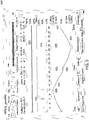
- Figure 4 depicts an illustration of diagnostic modeling display 400 of a conventional system that does not include an embodying waveform shaping circuit.
- Harmonic pane 410 depicts harmonic distribution across a frequency band of about 50-2500 Hz. It should be readily understood that in the frequency band of about 400-1200 Hz, there are multiple harmonics 412 that are above an acceptable threshold.
- Waveform pane 420 depicts models of ideal input current waveform 422, and impacted input current waveform 424. As can be observed, impacted waveform 424 includes perturbations at about voltage crossover points 426, 427. Similarly, high peak noise can be seen at input current peak 428, and input current valley 429.
- Figure 5 depicts an illustration of diagnostic modeling results 500 of an embodying system that includes a waveform shaping circuit in accordance with embodiments.
- Harmonic pane 510 depicts that an embodying system that includes a waveform shaping circuit generates harmonics 512 that are below predetermined threshold level 515.
- Waveform pane 520 depicts models of ideal input current waveform 522, and impacted input current waveform 524. As can be observed, impacted waveform 524 includes minimal perturbations at about current crossover points 526, 527. Similarly, waveform perturbations at input current peak 528, and input current valley 529 are no longer present.
- the model impacted waveform 524 indicates that instead of high spikes at the input waveform peak and valleys (as present in the conventional systems), the excursion of the peak and valley is reduced and smoothed by an embodying system that includes a waveform shaping circuit.
Landscapes
- Engineering & Computer Science (AREA)
- Computer Networks & Wireless Communication (AREA)
- Physics & Mathematics (AREA)
- Nonlinear Science (AREA)
- Mechanical Engineering (AREA)
- Signal Processing (AREA)
- Cable Transmission Systems, Equalization Of Radio And Reduction Of Echo (AREA)
Abstract
Description
- A Digital Addressable Lighting Interface (DALI) is a data and protocol standard for lighting and/or related equipment (e.g., ballasts, dimmers, photoelectric cells, transformers, motion detectors, etc.). DALI compatible equipment can be interconnected on a DALI bus, even if from different manufactures and of different lighting technologies. DALI requires a single pair of wires as the communication bus to all devices on the same DALI network. All devices connected to the network can be addressed by a broadcast message, or individual devices can be controlled with a unique bus address.
- A DALI network can include a controller and one or more lighting and/or related equipment devices having DALI interfaces. In some implementations, a DALI system can include a luminaire control unit (LCU), a luminaire (which can include a control unit and a LED light engine), and a data concentrator unit (DCU).
- The LCU can wirelessly communicate with the DCU via radio frequency transmissions (e.g., typically in the range 869.4-869.65 MHz, at 500 mW). The LCU can be series connected via wires/cables between a line voltage power source and the luminaire control unit. The LCU can switch off the luminaire by interrupting the line voltage power to the luminaire control unit. Additionally, the LCU could also include connections to the luminaire control unit via the DALI network.
- Individually, a conventional luminaire and a conventional LCU can each fulfill typical electromagnetic compatibility (EMC) requirements for spurious harmonic generation/suppression. However, when integrated at a system level this conventional equipment fails to meet specified EMC standards. When the LCU is active, RF communication with the DCU is non-predictable. The RF communication from the LCU to the DCU can cause generation of the unwanted harmonics. Further, the LCU's control of line voltage power to the luminaire control unit can result in high peak-current spikes, which themselves can generate unwanted harmonics. Thus, at a system level EMC standards are not often met by a DALI network containing an LCU, a DCU, and a luminaire.
-
-
FIG. 1 depicts a system with a waveform shaping circuit in accordance with embodiments; -
FIG. 2 depicts a system with a waveform shaping circuit in accordance with embodiments; -
FIG. 3 depicts a system with a waveform shaping circuit in accordance with embodiments; -
FIG. 4 depicts an illustration of diagnostic modeling results of a conventional system; and -
FIG. 5 depicts an illustration of diagnostic modeling results of an embodying system that includes a waveform shaping circuit in accordance with embodiments. - Embodying systems include a waveform shaping circuit between the line voltage power and a LCU and a luminaire associated with the LCU (a single LCU can provide independent control to one or more luminaires). In accordance with an embodiment, the waveform shaping circuit can be a series resistance (e.g., in the range of about 200-980 Ohm) and a bypass switch connected in parallel between the line voltage source and the LCU input. In accordance with some embodiments, the waveform shaping circuit can include ferrite line elements in conjunction with discrete circuit components.
- Embodying systems include the waveform shaping circuit to suppress unwanted spurious harmonics generated by operation of a conventional LCU in the control of a luminaire. These spurious harmonics can be caused due to the LCU having a high peak input current coincident with about the maximum swing (i.e., peak and valley) of each half period cycle of the AC input line voltage. The high peak input current can cause high total harmonic distortion (THD) on the line voltage, where one or more of the harmonics can have a high current. In contrast to conventional line filters that passively dissipate noise, embodying waveform shaping circuits decrease the generation of noise at its source by affecting the impedance match of the LCU to the input line voltage. Embodying devices do not merely dissipate noise, but rather eliminate the root cause of the noise generation. Accordingly, each embodiment of the waveform shaping circuit includes an impedance matching network that alters the input impedance of the LCU to minimize harmonic generation by the LCU.
-
Figure 1 depictssystem 100 that includeswaveform shaping circuit 110 in accordance with embodiments.Waveform shaping circuit 110 is external toLCU 120, which communicates withDCU 130 via RF signals.System 100 includes at least oneluminaire 140 controlled by the LCU. The luminaire can internally includecontrol unit 142,driver electronics 144, andlighting source 146. - RF communication by
LCU 120 toDCU 130 can generate spurious harmonics on the line (L) and neutral (N)voltage lines 150.Waveform shaping circuit 110 alters the input impedance ofLCU 120 as seen by the voltage lines to affect a better impedance match to reduce these spurious harmonics. In accordance with embodiments, waveform shaping circuit can be in series with the LCU input terminals and the line and the neutral voltage lines. -
Figure 2 depictssystem 200 that includeswaveform shaping circuit 210 in accordance with embodiments.Waveform shaping circuit 210 can be in series with the LCU voltage input terminal and the line voltage power source. In accordance with embodiments,waveform shaping circuit 210 can include series resistor 212 (e.g., having a resistance in the range of about 200-980 Ohms). Placement of a resistor of this value can generate an additional power consumption of up to about 0.5 W. This power consumption can be decreased by includingbypass switch 214, which can be controlled by the LCU tobypass series resistor 212 with an about zero, or low, resistance circuit when the current limitation is not needed (i.e., when the LCU is not active).Bypass switch 214 can be implemented by a semiconductor switch (e.g., transistor, MOSFET, JFET, TRIAC, etc.), a relay, and the like. -
Figure 3 depictssystem 300 that includeswaveform shaping circuit 310 in accordance with embodiments.Waveform shaping circuit 310 can includeinput ferrite choke 311, andoutput ferrite choke 312, each of which can suppress high frequency spurious harmonics present on the line and the neutral voltage lines. Across the input line voltage (between the line and the neutral lines), waveform shaping circuit can include capacitor C1 314 (having a capacitance of about 47 nF). Capacitor C1 can filter noise on the input voltages to suppress the spurious harmonics. Resistor R1 316 (having a resistance of about 470 Ohms), can be in series with the neutral line input toLCU 120. Capacitor C2 (having a capacitance of about 47 nF) is connected from the neutral line voltage to protected earth (PE)ground 319. Capacitor C2 can bypass spurious harmonics to the earth ground. -
Figure 4 depicts an illustration ofdiagnostic modeling display 400 of a conventional system that does not include an embodying waveform shaping circuit.Harmonic pane 410 depicts harmonic distribution across a frequency band of about 50-2500 Hz. It should be readily understood that in the frequency band of about 400-1200 Hz, there aremultiple harmonics 412 that are above an acceptable threshold. -
Waveform pane 420 depicts models of ideal inputcurrent waveform 422, and impacted inputcurrent waveform 424. As can be observed, impactedwaveform 424 includes perturbations at aboutvoltage crossover points current peak 428, and inputcurrent valley 429. -
Figure 5 depicts an illustration ofdiagnostic modeling results 500 of an embodying system that includes a waveform shaping circuit in accordance with embodiments.Harmonic pane 510 depicts that an embodying system that includes a waveform shaping circuit generatesharmonics 512 that are below predeterminedthreshold level 515.Waveform pane 520 depicts models of ideal inputcurrent waveform 522, and impacted inputcurrent waveform 524. As can be observed, impactedwaveform 524 includes minimal perturbations at aboutcurrent crossover points current peak 528, and inputcurrent valley 529 are no longer present. The model impactedwaveform 524 indicates that instead of high spikes at the input waveform peak and valleys (as present in the conventional systems), the excursion of the peak and valley is reduced and smoothed by an embodying system that includes a waveform shaping circuit. - Although specific hardware and methods have been described herein, note that any number of other configurations may be provided in accordance with embodiments of the invention. Thus, while there have been shown, described, and pointed out fundamental novel features of the invention, it will be understood that various omissions, substitutions, and changes in the form and details of the illustrated embodiments, and in their operation, may be made by those skilled in the art without departing from the spirit and scope of the invention. Substitutions of elements from one embodiment to another are also fully intended and contemplated. The invention is defined solely with regard to the claims appended hereto, and equivalents of the recitations therein.
Claims (10)
- A waveform shaping circuit (110, 210, 310) for a lighting system (100, 200, 300) that includes a lighting control unit (120) and at least one luminaire (140), the waveform shaping circuit (110, 210, 310) comprising:a line voltage input (L) (150) connectable to a line voltage power source (146);a line voltage output (150), the line voltage output connectable to an input voltage port of the lighting control unit (120);a neutral line input (N) connectable to a neutral line of the line voltage power source (146); andthe waveform shaping circuit (110, 210, 310) including an impedance matching network configured to alter an input impedance of the lighting control circuit.
- The waveform shaping circuit (110, 210, 310) of claim 1, including a neutral line output connectable to a neutral line input (N) port of the lighting control unit (120).
- The waveform shaping circuit (110, 210, 310) of claim 1 or claim 2, the impedance matching network including:a resistor (212) in series with the line voltage input (150); anda bypass switch (214) in parallel with the resistor (212).
- The waveform shaping circuit (110, 210, 310) of claim 3, including the bypass switch (214) actively controlled by the lighting control unit (120), wherein the lighting control unit (120) activates the bypass switch (214) during periods of lighting control unit (120) inactivity.
- The waveform shaping circuit (110, 210, 310) of any of claims 2 to 4, the impedance matching network including:a first ferrite choke (311) surrounding the line voltage input (150) and the neutral line input (N);a second ferrite choke (312) surrounding the lighting control unit (120) input line voltage port and the lighting control unit (120) neutral line input port;a shunt capacitor (314) located between the line voltage input (150) and the neutral line input (N);a bypass capacitor (318) located between the neutral line input (N) and a protected earth ground (319); anda resistor (316) in series between the neutral line input (N) and the lighting control unit (120) neutral line input port (N).
- A lighting system (100, 200, 300) comprising:a lighting control unit (120) in control communication with a luminaire (140), the lighting control unit (120) including a line voltage input port (L) and a neutral line input port (N);a waveform shaping circuit (110, 210, 310) comprising:a line voltage input (150) connectable to a line voltage power source (146);a line voltage output (150), the line voltage output connectable to the lighting control unit (120) input voltage port;a neutral line input (N) connectable to a neutral line of the line voltage power source (146); andthe waveform shaping circuit (110, 210, 310) including an impedance matching network configured to alter an input impedance of the lighting control circuit.
- The lighting system (100, 200, 300) of claim 6, the waveform shaping circuit (110, 210, 310) including a neutral line output connectable to the lighting control unit (120) neutral line input port (N).
- The lighting system (100, 200, 300) of claim 6 or claim 7, the impedance matching network including:a resistor (212) in series with the line voltage input (150); anda bypass switch (214) in parallel with the resistor (212).
- The lighting system (100, 200, 300) of claim 8, including the bypass switch (214) actively controlled by the lighting control unit (120), wherein the lighting control unit (120) activates the bypass switch (214) during periods of lighting control unit (120) inactivity.
- The lighting system (100, 200, 300) of any of claims 7 to 9, the impedance matching network including:a first ferrite choke (311) surrounding the line voltage input (150) and the neutral line input (N);a second ferrite choke (312) surrounding the lighting control unit (120) input line voltage port and the lighting control unit (120) neutral line input port (N);a shunt capacitor (314) located between the line voltage input (150) and the neutral line input (N);a bypass capacitor (318) located between the neutral line input (N) and a protected earth ground (319); anda resistor (316) in series between the neutral line input (N) and the lighting control unit (120) neutral line input port (N).
Applications Claiming Priority (1)
| Application Number | Priority Date | Filing Date | Title |
|---|---|---|---|
| US15/496,882 US10375796B2 (en) | 2017-04-25 | 2017-04-25 | Waveform shaping circuit for spurious harmonic suppression |
Publications (1)
| Publication Number | Publication Date |
|---|---|
| EP3396832A1 true EP3396832A1 (en) | 2018-10-31 |
Family
ID=62062892
Family Applications (1)
| Application Number | Title | Priority Date | Filing Date |
|---|---|---|---|
| EP18168956.3A Withdrawn EP3396832A1 (en) | 2017-04-25 | 2018-04-24 | A waveform shaping circuit for spurious harmonic suppression |
Country Status (3)
| Country | Link |
|---|---|
| US (1) | US10375796B2 (en) |
| EP (1) | EP3396832A1 (en) |
| CA (1) | CA3001147A1 (en) |
Families Citing this family (1)
| Publication number | Priority date | Publication date | Assignee | Title |
|---|---|---|---|---|
| US11506696B2 (en) * | 2020-10-15 | 2022-11-22 | Western Digital Technologies, Inc. | Hold-up capacitance health measurement with current leakage detection |
Citations (3)
| Publication number | Priority date | Publication date | Assignee | Title |
|---|---|---|---|---|
| US5703438A (en) * | 1996-01-22 | 1997-12-30 | Valmont Industries, Inc. | Line current filter for less than 10% total harmonic distortion |
| US20030001516A1 (en) * | 2001-06-22 | 2003-01-02 | Lutron Electronics Co., Inc | Electronic ballast |
| EP2592901A1 (en) * | 2011-11-10 | 2013-05-15 | Toshiba Lighting & Technology Corporation | Lighting power source and luminaire |
Family Cites Families (12)
| Publication number | Priority date | Publication date | Assignee | Title |
|---|---|---|---|---|
| US4277726A (en) * | 1978-08-28 | 1981-07-07 | Litton Systems, Inc. | Solid-state ballast for rapid-start type fluorescent lamps |
| JPH03116698A (en) | 1989-09-29 | 1991-05-17 | Toshiba Lighting & Technol Corp | Discharge lamp lighting device |
| DE9318071U1 (en) * | 1993-11-25 | 1995-03-23 | Patent-Treuhand-Gesellschaft für elektrische Glühlampen mbH, 81543 München | Circuit arrangement for operating a low-pressure discharge lamp on a low-voltage voltage source |
| US7602157B2 (en) * | 2005-12-28 | 2009-10-13 | Flyback Energy, Inc. | Supply architecture for inductive loads |
| KR101001241B1 (en) * | 2008-09-05 | 2010-12-17 | 서울반도체 주식회사 | AC LED dimmer and dimming method |
| US20120146525A1 (en) | 2009-04-24 | 2012-06-14 | City University Of Hong Kong | Apparatus and methods of operation of passive and active led lighting equipment |
| CA2785715A1 (en) | 2009-12-28 | 2011-07-28 | Paul M. Babcock | Controllable universal supply with reactive power management |
| CN102523666B (en) | 2012-01-16 | 2013-08-14 | 矽力杰半导体技术(杭州)有限公司 | High-efficiency LED (Light Emitting Diode) driving circuit and driving method thereof |
| BR112017002027A2 (en) * | 2014-07-31 | 2018-01-30 | Enel Sole Srl | fixed installation outdoor lighting adapted for connection to a mains to be supplied with mains supply voltage and external lighting system |
| US9475581B2 (en) * | 2014-10-08 | 2016-10-25 | Goodrich Corporation | Adjustable restraint assemblies |
| WO2016110833A2 (en) * | 2015-01-06 | 2016-07-14 | Cmoo Systems Itd. | A method and apparatus for power extraction in a pre-existing ac wiring infrastructure |
| CN107517520A (en) | 2015-05-08 | 2017-12-26 | 湖南工业大学 | A wall control switch that sends LED light brightness control signals through a single live wire |
-
2017
- 2017-04-25 US US15/496,882 patent/US10375796B2/en active Active
-
2018
- 2018-04-12 CA CA3001147A patent/CA3001147A1/en not_active Abandoned
- 2018-04-24 EP EP18168956.3A patent/EP3396832A1/en not_active Withdrawn
Patent Citations (3)
| Publication number | Priority date | Publication date | Assignee | Title |
|---|---|---|---|---|
| US5703438A (en) * | 1996-01-22 | 1997-12-30 | Valmont Industries, Inc. | Line current filter for less than 10% total harmonic distortion |
| US20030001516A1 (en) * | 2001-06-22 | 2003-01-02 | Lutron Electronics Co., Inc | Electronic ballast |
| EP2592901A1 (en) * | 2011-11-10 | 2013-05-15 | Toshiba Lighting & Technology Corporation | Lighting power source and luminaire |
Also Published As
| Publication number | Publication date |
|---|---|
| CA3001147A1 (en) | 2018-10-25 |
| US20180310382A1 (en) | 2018-10-25 |
| US10375796B2 (en) | 2019-08-06 |
Similar Documents
| Publication | Publication Date | Title |
|---|---|---|
| RU2624452C2 (en) | Interface digital communication circuit for wired pair with individually adjustable transition borders | |
| CN101933343B (en) | An electrostatic speaker system | |
| CN105939554B (en) | LED light modulating devices and LED drive power | |
| US10264635B2 (en) | Ripple suppression circuit and light emitting diode driver | |
| US20100253245A1 (en) | Method, system and current limiting circuit for preventing excess current surges | |
| US10938205B2 (en) | Electronic device | |
| CN112512180A (en) | DMX512 control circuit capable of meeting EMC requirements | |
| US10375796B2 (en) | Waveform shaping circuit for spurious harmonic suppression | |
| US10784678B1 (en) | Damped PI-type filter Y-type capacitance network for radiated and conducted emission | |
| CN104538963B (en) | Adaptive filter | |
| CN113328617B (en) | An active common mode electromagnetic interference filter, power management device and filtering method | |
| US10219332B2 (en) | Constant-current constant-voltage (CCCV) control unit power supply | |
| CN110191548A (en) | Bus multichannel regulating system and method, bus desk lamp with dimmer switch, DC mould group and DC lamps and lanterns | |
| US11737188B2 (en) | LED-driver with PFC and wired bus interface | |
| CN105144843A (en) | Operating device for luminous elements | |
| CN107071962B (en) | A kind of power supply and telecommunication circuit that can prevent high pressure damage | |
| CN211240230U (en) | Wireless ad hoc network type regulator for power track | |
| CN205142040U (en) | Power Circuit Isolation System | |
| CN206380143U (en) | A kind of power supply that can prevent high pressure from damaging and telecommunication circuit | |
| US20210168913A1 (en) | Remote power delivery for distributed lighting with integrated data transmission | |
| CN203608419U (en) | LED driver | |
| CN109818491A (en) | Power supply device and LED driving device | |
| CN209608343U (en) | A kind of DCS control system power supply and DCS control system | |
| CN209088805U (en) | A high voltage DC switching power supply and its filter circuit | |
| CN209675936U (en) | DC power supply and power supply device |
Legal Events
| Date | Code | Title | Description |
|---|---|---|---|
| PUAI | Public reference made under article 153(3) epc to a published international application that has entered the european phase |
Free format text: ORIGINAL CODE: 0009012 |
|
| STAA | Information on the status of an ep patent application or granted ep patent |
Free format text: STATUS: THE APPLICATION HAS BEEN PUBLISHED |
|
| AK | Designated contracting states |
Kind code of ref document: A1 Designated state(s): AL AT BE BG CH CY CZ DE DK EE ES FI FR GB GR HR HU IE IS IT LI LT LU LV MC MK MT NL NO PL PT RO RS SE SI SK SM TR |
|
| AX | Request for extension of the european patent |
Extension state: BA ME |
|
| STAA | Information on the status of an ep patent application or granted ep patent |
Free format text: STATUS: REQUEST FOR EXAMINATION WAS MADE |
|
| 17P | Request for examination filed |
Effective date: 20190430 |
|
| RBV | Designated contracting states (corrected) |
Designated state(s): AL AT BE BG CH CY CZ DE DK EE ES FI FR GB GR HR HU IE IS IT LI LT LU LV MC MK MT NL NO PL PT RO RS SE SI SK SM TR |
|
| STAA | Information on the status of an ep patent application or granted ep patent |
Free format text: STATUS: EXAMINATION IS IN PROGRESS |
|
| 17Q | First examination report despatched |
Effective date: 20200423 |
|
| STAA | Information on the status of an ep patent application or granted ep patent |
Free format text: STATUS: THE APPLICATION IS DEEMED TO BE WITHDRAWN |
|
| 18D | Application deemed to be withdrawn |
Effective date: 20201104 |