EP3396777A1 - Connection structure of high-frequency transmission line - Google Patents
Connection structure of high-frequency transmission line Download PDFInfo
- Publication number
- EP3396777A1 EP3396777A1 EP16878916.2A EP16878916A EP3396777A1 EP 3396777 A1 EP3396777 A1 EP 3396777A1 EP 16878916 A EP16878916 A EP 16878916A EP 3396777 A1 EP3396777 A1 EP 3396777A1
- Authority
- EP
- European Patent Office
- Prior art keywords
- conductor
- central conductor
- transmission line
- connection structure
- outer conductor
- Prior art date
- Legal status (The legal status is an assumption and is not a legal conclusion. Google has not performed a legal analysis and makes no representation as to the accuracy of the status listed.)
- Withdrawn
Links
Images


Classifications
-
- H—ELECTRICITY
- H01—ELECTRIC ELEMENTS
- H01P—WAVEGUIDES; RESONATORS, LINES, OR OTHER DEVICES OF THE WAVEGUIDE TYPE
- H01P5/00—Coupling devices of the waveguide type
- H01P5/08—Coupling devices of the waveguide type for linking dissimilar lines or devices
- H01P5/085—Coaxial-line/strip-line transitions
-
- H—ELECTRICITY
- H01—ELECTRIC ELEMENTS
- H01R—ELECTRICALLY-CONDUCTIVE CONNECTIONS; STRUCTURAL ASSOCIATIONS OF A PLURALITY OF MUTUALLY-INSULATED ELECTRICAL CONNECTING ELEMENTS; COUPLING DEVICES; CURRENT COLLECTORS
- H01R13/00—Details of coupling devices of the kinds covered by groups H01R12/70 or H01R24/00 - H01R33/00
- H01R13/62—Means for facilitating engagement or disengagement of coupling parts or for holding them in engagement
-
- H—ELECTRICITY
- H01—ELECTRIC ELEMENTS
- H01R—ELECTRICALLY-CONDUCTIVE CONNECTIONS; STRUCTURAL ASSOCIATIONS OF A PLURALITY OF MUTUALLY-INSULATED ELECTRICAL CONNECTING ELEMENTS; COUPLING DEVICES; CURRENT COLLECTORS
- H01R24/00—Two-part coupling devices, or either of their cooperating parts, characterised by their overall structure
- H01R24/38—Two-part coupling devices, or either of their cooperating parts, characterised by their overall structure having concentrically or coaxially arranged contacts
- H01R24/40—Two-part coupling devices, or either of their cooperating parts, characterised by their overall structure having concentrically or coaxially arranged contacts specially adapted for high frequency
-
- H—ELECTRICITY
- H01—ELECTRIC ELEMENTS
- H01R—ELECTRICALLY-CONDUCTIVE CONNECTIONS; STRUCTURAL ASSOCIATIONS OF A PLURALITY OF MUTUALLY-INSULATED ELECTRICAL CONNECTING ELEMENTS; COUPLING DEVICES; CURRENT COLLECTORS
- H01R9/00—Structural associations of a plurality of mutually-insulated electrical connecting elements, e.g. terminal strips or terminal blocks; Terminals or binding posts mounted upon a base or in a case; Bases therefor
- H01R9/03—Connectors arranged to contact a plurality of the conductors of a multiconductor cable, e.g. tapping connections
- H01R9/05—Connectors arranged to contact a plurality of the conductors of a multiconductor cable, e.g. tapping connections for coaxial cables
-
- H—ELECTRICITY
- H03—ELECTRONIC CIRCUITRY
- H03H—IMPEDANCE NETWORKS, e.g. RESONANT CIRCUITS; RESONATORS
- H03H7/00—Multiple-port networks comprising only passive electrical elements as network components
- H03H7/38—Impedance-matching networks
-
- H—ELECTRICITY
- H01—ELECTRIC ELEMENTS
- H01R—ELECTRICALLY-CONDUCTIVE CONNECTIONS; STRUCTURAL ASSOCIATIONS OF A PLURALITY OF MUTUALLY-INSULATED ELECTRICAL CONNECTING ELEMENTS; COUPLING DEVICES; CURRENT COLLECTORS
- H01R12/00—Structural associations of a plurality of mutually-insulated electrical connecting elements, specially adapted for printed circuits, e.g. printed circuit boards [PCB], flat or ribbon cables, or like generally planar structures, e.g. terminal strips, terminal blocks; Coupling devices specially adapted for printed circuits, flat or ribbon cables, or like generally planar structures; Terminals specially adapted for contact with, or insertion into, printed circuits, flat or ribbon cables, or like generally planar structures
- H01R12/50—Fixed connections
- H01R12/51—Fixed connections for rigid printed circuits or like structures
- H01R12/55—Fixed connections for rigid printed circuits or like structures characterised by the terminals
- H01R12/57—Fixed connections for rigid printed circuits or like structures characterised by the terminals surface mounting terminals
-
- H—ELECTRICITY
- H01—ELECTRIC ELEMENTS
- H01R—ELECTRICALLY-CONDUCTIVE CONNECTIONS; STRUCTURAL ASSOCIATIONS OF A PLURALITY OF MUTUALLY-INSULATED ELECTRICAL CONNECTING ELEMENTS; COUPLING DEVICES; CURRENT COLLECTORS
- H01R2103/00—Two poles
-
- H—ELECTRICITY
- H01—ELECTRIC ELEMENTS
- H01R—ELECTRICALLY-CONDUCTIVE CONNECTIONS; STRUCTURAL ASSOCIATIONS OF A PLURALITY OF MUTUALLY-INSULATED ELECTRICAL CONNECTING ELEMENTS; COUPLING DEVICES; CURRENT COLLECTORS
- H01R24/00—Two-part coupling devices, or either of their cooperating parts, characterised by their overall structure
- H01R24/38—Two-part coupling devices, or either of their cooperating parts, characterised by their overall structure having concentrically or coaxially arranged contacts
- H01R24/40—Two-part coupling devices, or either of their cooperating parts, characterised by their overall structure having concentrically or coaxially arranged contacts specially adapted for high frequency
- H01R24/50—Two-part coupling devices, or either of their cooperating parts, characterised by their overall structure having concentrically or coaxially arranged contacts specially adapted for high frequency mounted on a PCB [Printed Circuit Board]
-
- H—ELECTRICITY
- H01—ELECTRIC ELEMENTS
- H01R—ELECTRICALLY-CONDUCTIVE CONNECTIONS; STRUCTURAL ASSOCIATIONS OF A PLURALITY OF MUTUALLY-INSULATED ELECTRICAL CONNECTING ELEMENTS; COUPLING DEVICES; CURRENT COLLECTORS
- H01R9/00—Structural associations of a plurality of mutually-insulated electrical connecting elements, e.g. terminal strips or terminal blocks; Terminals or binding posts mounted upon a base or in a case; Bases therefor
- H01R9/03—Connectors arranged to contact a plurality of the conductors of a multiconductor cable, e.g. tapping connections
- H01R9/05—Connectors arranged to contact a plurality of the conductors of a multiconductor cable, e.g. tapping connections for coaxial cables
- H01R9/0515—Connection to a rigid planar substrate, e.g. printed circuit board
Definitions
- the present invention relates to a connection structure of a high-frequency transmission line and to, for example, a connection structure that connects a coaxial line and a planar transmission line.
- coaxial line and a coplanar line as high-frequency transmission lines for transmission of a high-frequency signal such as a microwave or millimeter wave signal.
- non-patent literature 1 discloses a connection structure of an arrangement in which the axis of a signal line between a coaxial line and a coplanar line is continuously shifted toward the coplanar line from the center of the coaxial line.
- Non-Patent Literature 1 R.L. Eisenhart, "A BETTER MICROSTRIP CONNECTOR", Microwave Symposium Digest, IEEE-MTT-S International, 27 - 29 June 1978 P. 318 - P. 320 .
- Figs. 15 to 17 are views each showing the conventional connection structure.
- Fig. 15 shows the sectional shape of the side surface of a conventional connection structure 90 of a coaxial line and a coplanar line.
- Fig. 16 shows the sectional shape of the upper surface of the conventional connection structure 90.
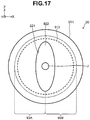
- Fig. 17 shows the planar shape of the conventional connection structure 90 when viewed from a Y-axis direction. Note that in Fig. 17 , a substrate 200, a connection block 8 for connecting the substrate 200 and a central conductor 7, and a metal member 10 are not illustrated.
- the conventional connection structure 90 of the coaxial line and the coplanar line includes a coaxial mode block 91 connected to a coaxial line 1, and a coplanar mode block 92 connected to the coplanar line formed on the substrate 200.
- the coaxial mode block 91 is formed from the central conductor 7, as an inner conductor, having one end connected to the coaxial line 1 and the other end connected, via the pedestal 8, to the coplanar line formed on the substrate 200, a dielectric body 912 covering the central conductor 7, and an outer conductor 911 covering the dielectric body 912.
- the coplanar mode block 92 is formed from an outer conductor 921 having an elliptic hole formed by processing the metal member 10, and a dielectric body 922 filled between the hole of the outer conductor 921 and the central conductor 7.
- the connection structure 90 shown in Figs. 15 to 17 includes a boundary portion between the coaxial mode block 91 and the coplanar mode block 92, that is, edge regions 93A and 93B where the surface of the coaxial mode block 91 intersects the surface of the coplanar mode block 92.
- the surface of the metal member 10 contacting the coaxial mode block 91 is close to the surface of the outer conductor 921 of the coplanar mode block 92. Since, in the edge regions 93A and 93B, the areas of the surfaces close to each other are relatively large, an electric field is concentrated, and a mismatch between electromagnetic field modes occurs. This eventually causes a problem of parasitic capacitances generated in the edge regions 93A and 93B, and deterioration of the transmission characteristic between the coaxial line and the coplanar line.
- connection structure in which the axis of the signal line between the coaxial line and the coplanar line is continuously shifted toward the coplanar line from the center of the coaxial line, as described in the above non-patent literature 1, it is not easy to process the metal member for implementing a shape in which the axis of the signal line is continuously shifted.
- the present invention has been made in consideration of the above problems, and has as its object to provide a connection structure of a high-frequency transmission line having excellent processability, which is also capable of suppressing deterioration in signal transmission characteristics.
- a connection structure of a high-frequency transmission line that connects a coaxial line and a planar transmission line, including a columnar central conductor having one end connected to an inner conductor of the coaxial line and the other end connected to the planar transmission line, a first outer conductor including a first hole that is formed coaxially with the central conductor and is larger than an outer diameter of the central conductor, and arranged on a side of the one end of the central conductor, a first dielectric body filled between the central conductor and the first outer conductor, a second outer conductor including a second hole that is formed coaxially with the central conductor and is larger than the outer diameter of the central conductor, and arranged on a side of the other end of the central conductor, a second dielectric body filled between the central conductor and the second outer conductor, a third outer conductor including a third hole that is formed coaxially with the central conductor and is larger than the outer diameter of the central conductor, and arranged between the first outer
- connection structure of a high-frequency transmission line having excellent processability, which is also capable of suppressing deterioration in signal transmission characteristics.
- connection structure (3; 13; 23) of a high-frequency transmission line that connects a coaxial line (1) and a planar transmission line (2), including a columnar central conductor (7) having one end connected to an inner conductor of the coaxial line and the other end connected to the planar transmission line, a first outer conductor (41) including a first hole (10A) that is formed coaxially with the central conductor and is larger than an outer diameter of the central conductor, and arranged on a side of the one end of the central conductor, a first dielectric body (42) filled between the central conductor and the first outer conductor, a second outer conductor (61; 63) including a second hole (10B) that is formed coaxially with the central conductor and is larger than the outer diameter of the central conductor, and arranged on a side of the other end of the central conductor, a second dielectric body (62) filled between the central conductor and the second outer conductor, a third outer conductor (51; 53) including a
- the second outer conductor (61) and the third outer conductor (51) are integrally formed by a single metal member (10).
- the third dielectric body (52) is air.
- the third hole is formed from a plurality of holes (10G, 10H) having different sizes and arranged in the axial (Y) direction of the central conductor.
- Figs. 1 to 4 are views each schematically showing a connection structure of a high-frequency transmission line according to an embodiment of the present invention.
- Fig. 1 is a perspective view schematically showing a connection structure 3 of a high-frequency transmission line according to the first embodiment.
- Fig. 2 shows a sectional shape viewed from an X-axis direction when cutting the connection structure 3 of the high-frequency transmission line along a Y-Z axial plane.
- Fig. 3 shows a sectional shape viewed from a Z-axis direction when cutting the connection structure 3 of the high-frequency transmission line along an X-Y axial plane.
- Fig. 4 shows the planar shape of the connection structure 3 of the high-frequency transmission line when viewed from a Y-axis direction. Note that in Fig. 4 , a substrate 200, a pedestal 8, and a metal member 10 are not illustrated.
- connection structure 3 of the high-frequency transmission line shown in Figs. 1 to 4 is a connection structure between different types of transmission lines, that relays the different types of transmission lines, and is, for example, a connection structure for relaying a coaxial line 1 and a planar transmission line 2 as high-frequency transmission lines each for transmitting a high-frequency signal such as a microwave or millimeter wave signal.
- the coaxial line 1 is a transmission line obtained by coaxially arranging an inner conductor and an outer conductor to sandwich a dielectric body, and is, for example, a high-frequency coaxial cable. Note that in Figs. 1 to 4 , the internal structure of the coaxial line 1 is not illustrated.
- the planar transmission line 2 is a transmission line obtained by patterning a signal wiring 201 and a ground wiring 202, both of which are made of a metal, on the substrate 200 formed from a dielectric body, and is, for example, a coplanar line or a microstrip line.
- the dielectric body forming the substrate 200 can be alumina, quartz, or a resin.
- planar line 2 is a coplanar line
- the ground wiring 202 is formed around the signal wiring 201 on the substrate 200.
- connection structure 3 of the high-frequency transmission line has a structure in which the metal member 10 is provided with a coaxial mode block 4 electrically connected to the coaxial line 1, a coplanar mode block 6 electrically connected to the planar transmission line 2, and a buffer block 5 arranged between the coaxial mode block 4 and the coplanar mode block 6.
- the metal member 10 is made of a conductive material, and serves as the base of the connection structure 3 of the high-frequency transmission line while supporting the planar transmission line 2.
- Examples of the material of the metal member 10 can be metallic materials such as copper (Cu), aluminum (Al), and kovar.
- the coaxial mode block 4 includes a central conductor 7, an outer conductor 41, and a dielectric body 42.
- the central conductor 7 is made of a columnar conductive material having one end connected to the inner conductor of the coaxial line 1 and the other end connected to the signal wiring 201 of the planar transmission line 2.
- An example of the above material can be a metallic material such as copper or kovar.
- the outer conductor 41 is coaxially spaced apart from the central conductor 7 on the one end side of the central conductor 7, that is connected to the coaxial line 1. More specifically, the outer conductor 41 includes a hole 41A that is formed coaxially with the central conductor 7 and is larger than the outer diameter of the central conductor 7, and is arranged on the one end side of the central conductor 7. Similarly to the central conductor 7, the outer conductor 41 is made of a conductive metallic material such as copper or kovar.
- the outer conductor 41 is formed from a first tubular portion 411 having an outer diameter R1 corresponding to the coaxial line 1, and a second tubular portion 412 that is joined to the first tubular portion 411 in the axial direction of the central conductor 7 and has an outer diameter R2 smaller than the outer diameter R1 of the first tubular portion 411.
- the dielectric body 42 is filled between the central conductor 7 and the outer conductor 41.
- An example of the dielectric body 42 can be a glass material (for example, a relative dielectric constant: about 4.0).
- the central conductor 7, the outer conductor 41, and the dielectric body 42 form one connector 40.
- the connector 40 by inserting the connector 40 into a hole 10A that is formed in advance in the metal member 10 in accordance with the shape of the connector 40, the coaxial mode block 4 is disposed in the metal member 10.
- the coplanar mode block 6 includes an outer conductor 61 and a dielectric body 62.
- the outer conductor 61 is coaxially spaced apart from the central conductor 7 on the other end side (the side of the planar transmission line 2) of the central conductor 7. More specifically, the outer conductor 61 includes a hole 10B that is formed coaxially with the central conductor 7 and is larger than the outer diameter of the central conductor 7, and is arranged on the other end side of the central conductor 7.
- a partial region of the metal member 10, where the hole 10B is formed, is used as the outer conductor 61.
- the hole 10B of the outer conductor 61 is formed into a rectangular shape in which the length in the Z-axis direction is longer than that of in the X-axis direction when viewed from the Y-axis direction. More specifically, the hole 10B is formed into a rectangular shape having four rounded corners.
- the dielectric body 62 is filled between the central conductor 7 and the outer conductor 61.
- an example of the dielectric body 62 can be a glass material.
- the buffer block 5 includes an outer conductor 51 and a dielectric body 52.
- the outer conductor 51 is coaxially spaced apart from the central conductor 7 between the outer conductors 41 and 61 in the axial direction of the central conductor 7. More specifically, the outer conductor 51 includes a hole 10C that is formed coaxially with the central conductor 7 and is larger than the outer diameter of the central conductor, and is arranged between the outer conductors 41 and 61.
- a partial region of the metal member 10, where the hole 10C is formed is used as the outer conductor 51, similarly to the outer conductor 61.
- the hole 10C of the outer conductor 51 is formed into a rectangular shape in which the length in the Z-axis direction is longer than that of in the X-axis direction when viewed from the Y-axis direction. More specifically, the hole 10C is formed into a rectangular shape having four rounded corners.
- the dielectric body 52 is filled between the central conductor 7 and the outer conductor 51.
- the dielectric body 52 has a relative dielectric constant lower than that of the dielectric body 42.
- the dielectric body 52 is air (relative dielectric constant: about 1.0), and forms a coaxial tube (a coaxial line having a so-called air coaxial structure) together with the central conductor 7 and the outer conductor 51.
- a fluororesin (relative dielectric constant: 2.0 to 3.0) can be used as the dielectric body 52, instead of air.
- the buffer block 5 is arranged in a region inside the coaxial mode block 4 when viewed from the axial direction (Y-axis direction) of the central conductor 7. More specifically, the dielectric body 52 of the buffer block 5 is arranged inside a region filled with the dielectric body 42 when viewed from the Y-axis direction.
- At least part of the coplanar mode block 6 is arranged in a region inside the buffer block 5 when viewed from the axial direction (Y-axis direction) of the central conductor 7. More specifically, at least part of the dielectric body 62 of the coplanar mode block 6 is arranged inside a region filled with the dielectric body 52 forming the buffer block 5 when viewed from the Y-axis direction. That is, two end portions in the Z-axis direction of the elliptic coplanar mode block 6 are arranged inside the buffer block 5 when viewed from the Y-axis direction. On the other hand, two end portions in the Z-axis direction of the elliptic coplanar mode block 6 are arranged outside the buffer block 5.
- a shortest distance between the central conductor 7 and the outer conductor 41 (the inner wall surface of the outer conductor 41 contacting the dielectric body 42), that of between the central conductor 7 and the outer conductor 51, and that of between the central conductor 7 and the outer conductor 61 are represented by x1, x2, and x3, respectively, x3 ⁇ x2 ⁇ x1 holds.
- the buffer block 5 and the coplanar mode block 6 are arranged so that the lengths in the X-axis direction (widthwise direction) of the outer conductors 41, 51, 61 in a signal path from the coaxial mode to the coplanar mode gradually decrease.
- the thickness of the buffer block 5, that is, the length in the Y-axis direction of the dielectric body 52 need only be a length that can suppress generation of a parasitic capacitance at the boundary between the coaxial mode block 4 (connector 40) and the coplanar mode block 6. More specifically, the length need only be 1/4 wavelength of an electromagnetic wave used for transmission or less. When, for example, the electromagnetic wave has a frequency of 90 GHz, the length need only fall within the range of, for example, 0.15 mm to 0.75 mm.
- Figs. 7 and 8 each show a transmission characteristic simulation result of the connection structure according to this embodiment.
- Fig. 7 shows a TDR (Time Domain Reflectometry) simulation result 700 of the connection structure 3 of the high-frequency transmission line according to the first embodiment, and a TDR simulation result 701 of the conventional connection structure 90 as a comparative example.
- the abscissa represents time [ps] and the ordinate represents a characteristic impedance [ ⁇ ].
- Fig. 8 shows a transmission characteristic simulation result 800 of the connection structure 3 of the high-frequency transmission line according to the first embodiment, and a transmission characteristic simulation result 801 of the conventional connection structure 90 as a comparative example.
- the abscissa represents a frequency [GHz] and the ordinate represents S21 [dB] of S-parameters.
- connection structure 3 that connects the coaxial line 1 and the planar transmission line (coplanar line) 2 shown in Fig. 1 is used as a simulation model
- kovar is used as the metallic material of the central conductor 7, outer conductor 41, and metal member 10 (outer conductors 51 and 61)
- air is used as the dielectric body 52 (thickness: 0.15 mm) of the buffer block 5
- a glass material having a relative dielectric constant of about 4.0 is used as the dielectric bodies 42 and 62.
- connection structure 3 can improve the transmission characteristic, as compared to the conventional connection structure 90, by providing the buffer block 5 to suppress generation of a parasitic capacitance between the coaxial mode block 4 (connector 40) and the coplanar mode block 6. Especially, as shown in Fig. 8 , it is possible to suppress deterioration in transmission characteristic at a frequency of 80 GHz or higher, as compared to the conventional connection structure 90.
- connection structure 3 of the high-frequency transmission line according to the first embodiment is configured such that the buffer block 5 is provided between the coaxial mode block 4 and the coplanar mode block 6 and the lengths in the X-axis direction (widthwise direction) of the outer conductors 41, 51, and 61 in the signal path from the axial mode to the coplanar mode gradually decrease. That is, in the connection structure 3 of the high-frequency transmission line according to the first embodiment, the coaxial mode block 4 and the coplanar mode block 6 are connected via the buffer block 5 having an intermediate mode between the coaxial mode and the coplanar mode, instead of directly switching between the coaxial mode in which an electromagnetic field spreads radially and the coplanar mode in which an electromagnetic field spreads in the horizontal direction.
- connection structure 3 of the high-frequency transmission line according to the first embodiment can suppress deterioration in transmission characteristic, as compared to the above-described conventional connection structure 90.
- connection structure 3 of the high-frequency transmission line it is not necessary to form a shape in which the center of the coplanar mode block 6 is shifted from the coaxial mode block 4, unlike the connection structure disclosed in non-patent literature 1. Therefore, it is easy to process the metal member 10 when forming the coplanar mode block 6 and the coaxial mode block 4, thereby providing a connection structure with excellent processability.
- the hole 10C can be readily formed by inserting a drill in a direction (Y-axis direction) perpendicular to the X-Z plane of the metal member 10 and shifting it in the Z-axis direction to cut the metal member 10. The same applies to the hole 10B.
- the outer conductors 51 and 61 may be easier to design the high-frequency transmission line by forming the outer conductors 51 and 61 into a rectangular shape, that is, a shape having straight lines. For example, it may be easier to adjust the characteristic impedance to a desired value (for example, 50 ⁇ ).
- Figs. 9 to 11 are views each showing a connection structure of a high-frequency transmission line according to the second embodiment.
- Fig. 9 shows a sectional shape viewed from an X-axis direction when cutting a connection structure 13 of the high-frequency transmission line along a Y-Z axial plane.
- Fig. 10 shows a sectional shape viewed from a Z-axis direction when cutting the connection structure 13 of the high-frequency transmission line along an X-Y axial plane.
- Fig. 11 shows the planar shape of the connection structure 13 of the high-frequency transmission line when viewed from a Y-axis direction. Note that in Fig. 11 , a substrate 200, a pedestal 8, and a metal member 10 are not illustrated.
- connection structure 13 of the high-frequency transmission line according to the second embodiment is different from the connection structure 3 of the high-frequency transmission line according to the first embodiment in terms of the arrangements of a buffer block and a coplanar mode block.
- the remaining structures are the same as in the connection structure 3 of the high-frequency transmission line according to the first embodiment.
- the same reference numerals as in the connection structure 3 according to the first embodiment denote the same constituent elements and a detailed description thereof will be omitted.
- a buffer block 15 includes an outer conductor 53 and a dielectric body 52.
- the outer conductor 53 is coaxially spaced apart from a central conductor 7 between outer conductors 41 and 63 in the axial direction of the central conductor 7. More specifically, the outer conductor 53 includes a hole 10F that is formed coaxially with the central conductor 7 and is larger than the outer diameter of the central conductor 7, and is arranged between the outer conductors 41 and 63.
- the hole 10F in the metal member 10 a partial region of the metal member 10, where the hole 10F is formed, is used as the outer conductor 53, similarly to the outer conductor 51 according to the first embodiment.
- the dielectric body 52 is filled between the outer conductor 53 and the central conductor 7.
- the hole 10F is formed into a circular shape when viewed from the Y-axis direction. More specifically, when viewed from the Y-axis direction, the hole 10F (dielectric body 52) has a circular shape with a diameter smaller than that of a hole 10A of a coaxial mode block 4 (the outer circumferential circle of a dielectric body 42), and is arranged inside a region filled with the dielectric body 42 of the coaxial mode block 4.
- a coplanar mode block 16 includes an outer conductor 63 and a dielectric body 62.
- the outer conductor 63 is coaxially spaced apart from the central conductor 7 on the other end side (the side of a planar transmission line 2) of the central conductor 7. More specifically, the outer conductor 63 includes a hole 10E that is larger than the outer diameter of the central conductor 7, and the other end of the central conductor 7 is arranged coaxially with the hole 10E in the hole 10E.
- the hole 10E in the metal member 10 a partial region of the metal member 10, where the hole 10E is formed, is used as the outer conductor 63, similarly to the outer conductor 61 according to the first embodiment.
- the dielectric body 62 is filled between the outer conductor 63 and the central conductor 7.
- the hole 10E (dielectric body 62) is formed into a rectangular shape when viewed from the Y-axis direction. More specifically, the hole 10E (dielectric body 62) has a rectangular shape with four rounded corners when viewed from the Y-axis direction, and is arranged inside a region filled with the dielectric body 52 of the buffer block 15.
- the thickness of the buffer block 15 need only be a length that can suppress generation of a parasitic capacitance at the boundary between the coaxial mode block 4 (a connector 40) and the coplanar mode block 6.
- the buffer block 15 and the coplanar mode block 16 are arranged so that the lengths in the X-axis direction (widthwise direction) of the outer conductors 41, 53, 63 in a signal path from the coaxial mode to the coplanar mode gradually decrease. More specifically, as shown in Fig.
- a shortest distance between the central conductor 7 and the outer conductor 41, that of between the central conductor 7 and the outer conductor 53, and that of between the central conductor 7 and the outer conductor 63 are represented by x1, x2, and x3, respectively, x3 ⁇ x2 ⁇ x1 holds.
- connection structure 13 according to the second embodiment is configured so that the coaxial mode block 4 (connector 40) and the coplanar mode block 6 are arranged to sandwich the buffer block 15 in the Y-axis direction and the lengths in the X-axis direction (widthwise direction) of the outer conductors 41, 53, and 63 in the signal path from the axial mode to the coplanar mode gradually decrease.
- This can prevent an electric field from being concentrated at the boundary between the coaxial mode block 4 and the coplanar mode block 6, thereby suppressing deterioration in transmission characteristic, as compared to the above-described conventional connection structure 90.
- Figs. 12 to 14 are views each showing a connection structure of a high-frequency transmission line according to the third embodiment.
- Fig. 12 shows the sectional shape of the side surface of a connection structure 23 of the high-frequency transmission line according to the third embodiment.
- Fig. 13 is a plan view showing the connection structure 23 of the high-frequency transmission line when viewed from a Y direction.
- Fig. 14 is an enlarged view showing a partial region of the connection structure 23 shown in Fig. 12 .
- connection structure 23 of the high-frequency transmission line according to the third embodiment is different from the connection structure 13 of the high-frequency transmission line according to the second embodiment in that a plurality of buffer blocks of different sizes are included.
- the remaining structures are the same as that of in the connection structure 13 of the high-frequency transmission line according to the second embodiment.
- connection structure 23 according to the third embodiment the same reference numerals as in the connection structure 13 according to the second embodiment denote the same constituent elements and a detailed description thereof will be omitted.
- connection structure 23 of the high-frequency transmission line includes two buffer blocks 25A and 25B arranged in the Y-axis direction between a coaxial mode block 4 and a coplanar mode block 6.
- the buffer blocks 25A and 25B are coaxially arranged.
- the buffer block 25A includes an outer conductor 53A and a dielectric body 52A. Similarly to the outer conductor 53 according to the second embodiment, the outer conductor 53A is coaxially spaced apart from a central conductor 7 between outer conductors 41 and 63 in the axial direction of the central conductor 7. More specifically, the outer conductor 53A includes a hole 10G that is formed coaxially with the central conductor 7 and is larger than the outer diameter of the central conductor 7, and is arranged between the outer conductors 41 and 63.
- the hole 10G in a metal member 10, a partial region of the metal member 10, where the hole 10G is formed, is used as the outer conductor 53A, similarly to the outer conductor 51 according to the first embodiment.
- the dielectric body 52A is filled between the outer conductor 53A and the central conductor 7.
- the hole 10G is formed into a circular shape when viewed from the Y-axis direction. More specifically, when viewed from the Y-axis direction, the hole 10G (dielectric body 52A) has a circular shape with a diameter smaller than that of a hole 10A of the coaxial mode block 4 (the outer circumferential circle of a dielectric body 42), and is arranged inside a region filled with the dielectric body 42 of the coaxial mode block 4.
- the buffer block 25B includes an outer conductor 53B and a dielectric body 52B. Similarly to the outer conductor 53 according to the second embodiment, the outer conductor 53B is coaxially spaced apart from the central conductor 7 between the outer conductors 41 and 63 in the axial direction of the central conductor 7.
- the outer conductor 53B includes a hole 10H that is formed coaxially with the central conductor 7 and is larger than the outer diameter of the central conductor 7, and is arranged between the outer conductors 41 and 63.
- the hole 10H in the metal member 10 a partial region of the metal member 10, where the hole 10H is formed, is used as the outer conductor 53B, similarly to the outer conductor 53A.
- the dielectric body 52B is filled between the outer conductor 53B and the central conductor 7.
- the hole 10H is formed into a circular shape when viewed from the Y-axis direction. More specifically, when viewed from the Y-axis direction, the hole 10H (dielectric body 52B) has a circular shape with a diameter smaller than that of the hole 10A of the coaxial mode block 4 (the outer circumferential circle of the dielectric body 42), and is arranged inside the region filled with the dielectric body 42 of the coaxial mode block 4. The diameter of the hole 10H is smaller than that of the hole 10G.
- a buffer block 15 and a coplanar mode block 16 are arranged so that the lengths in the X-axis direction (widthwise direction) of the outer conductors 41, 53A, 53B, and 63 in a signal path from the axial mode to the coplanar mode gradually decrease. More specifically, as shown in Fig.
- a shortest distance between the central conductor 7 and the outer conductor 41, that of between the central conductor 7 and the outer conductor 53A, that of between the central conductor 7 and the outer conductor 53B, and that of between the central conductor 7 and the outer conductor 63 are represented by x1, xa, xb, and x3, respectively, x3 ⁇ xb ⁇ xa ⁇ x1 holds.
- the hole 10G is filled with the dielectric body 52A
- the hole 10H is filled with the dielectric body 52B.
- the dielectric bodies 52A and 52B may be made of the same dielectric material or different dielectric materials, and the present invention is not particularly limited.
- both of the dielectric bodies 52A and 52B may be air (relative dielectric constant: about 1.0) or a fluororesin (relative dielectric constant: 2.0 to 3.0).
- a fluororesin may be used as the dielectric body 52A on the side of the coaxial mode block 4, and air may be used as the dielectric body 52B on the side of the coplanar mode block 6. This facilitates smoother switching between the coaxial mode and the coplanar mode.
- connection structure 23 of the high-frequency transmission line according to the third embodiment can prevent an electric field from being concentrated at the boundary portion between the coaxial mode block 4 and the coplanar mode block 6, thereby suppressing deterioration in transmission characteristic.
- connection structure 23 of the high-frequency transmission line according to the third embodiment is provided with the plurality of buffer blocks, it is easy to finely adjust the characteristic impedance.
- the above embodiments have exemplified a case in which the dielectric body 52 forming the buffer block 5 is air.
- the present invention is not limited to this, and another dielectric material may be used in accordance with the target characteristic impedance.
- the dielectric body 42 of the coaxial mode block 4 or the dielectric body 62 of the coplanar mode block 6 is not limited to the above-described glass material, and another dielectric material such as air may be used.
- the connector 40 convex in the Y-axis direction is used as the coaxial mode block 4.
- a portion of the metal member 10 may be used as the outer conductors 41 and 42 by processing the metal member 10 in accordance with the shape of the connector 40 without providing the connector 40.
- the processed metal member 10 need only be directly filled with the dielectric body 42.
- a connector formed from dielectric bodies forming the outer conductors 51 and 61 may be prepared, and arranged in the holes 10B and 10C formed in the metal member 10.
- a connector forming the outer conductors 51 and 61 may be fixed onto the metal member 10 without forming the holes 10B and 10C in the metal member 10.
- examples of the dielectric bodies forming the connector can be metallic materials such as copper or kovar.
- the third embodiment has exemplified a case in which the two buffer blocks 25A and 25B are provided between the coaxial mode block 4 and the coplanar mode block 6.
- the number of buffer blocks is not limited to two, and may be three or more.
- each of the outer conductors 51, 53, 53A, 53B, 61, and 63 are not limited to the rectangular shape or the circular shape as long as the lengths in the X-axis direction (widthwise direction) of the outer conductors in the signal path from the coaxial mode to the coplanar mode gradually decrease.
- each of the outer conductors 61 and 63 may have an elliptic shape in which the length in the Z-axis direction is longer than that of in the X-axis direction when viewed from the Y-axis direction.
- connection structure of the high-frequency transmission line can be applied as a connection structure of a high-frequency transmission line for transmission of a high-frequency signal such as a microwave or millimeter wave signal.
Landscapes
- Coupling Device And Connection With Printed Circuit (AREA)
- Waveguides (AREA)
- Waveguide Connection Structure (AREA)
Abstract
Description
- The present invention relates to a connection structure of a high-frequency transmission line and to, for example, a connection structure that connects a coaxial line and a planar transmission line.
- There are known a coaxial line and a coplanar line as high-frequency transmission lines for transmission of a high-frequency signal such as a microwave or millimeter wave signal.
- In a high-frequency transmission line, a single transmission line may be achieved by connecting different types of transmission lines. In such a case, it is necessary to connect the different types of transmission lines yet still suppressing deterioration in transmission characteristics. For example, non-patent
literature 1 discloses a connection structure of an arrangement in which the axis of a signal line between a coaxial line and a coplanar line is continuously shifted toward the coplanar line from the center of the coaxial line. - Non-Patent Literature 1: R.L. Eisenhart, "A BETTER MICROSTRIP CONNECTOR", Microwave Symposium Digest, IEEE-MTT-S International, 27 - 29 June 1978 P. 318 - P. 320.
- However, the present inventors have found that the conventional connection structure of the coaxial line and the coplanar line described in
non-patent literature 1 contains the following problems. -
Figs. 15 to 17 are views each showing the conventional connection structure.Fig. 15 shows the sectional shape of the side surface of aconventional connection structure 90 of a coaxial line and a coplanar line.Fig. 16 shows the sectional shape of the upper surface of theconventional connection structure 90.Fig. 17 shows the planar shape of theconventional connection structure 90 when viewed from a Y-axis direction. Note that inFig. 17 , asubstrate 200, aconnection block 8 for connecting thesubstrate 200 and acentral conductor 7, and ametal member 10 are not illustrated. - As shown in
Figs. 15 to 17 , theconventional connection structure 90 of the coaxial line and the coplanar line includes acoaxial mode block 91 connected to acoaxial line 1, and acoplanar mode block 92 connected to the coplanar line formed on thesubstrate 200. Thecoaxial mode block 91 is formed from thecentral conductor 7, as an inner conductor, having one end connected to thecoaxial line 1 and the other end connected, via thepedestal 8, to the coplanar line formed on thesubstrate 200, adielectric body 912 covering thecentral conductor 7, and anouter conductor 911 covering thedielectric body 912. Thecoplanar mode block 92 is formed from anouter conductor 921 having an elliptic hole formed by processing themetal member 10, and adielectric body 922 filled between the hole of theouter conductor 921 and thecentral conductor 7. - The
connection structure 90 shown inFigs. 15 to 17 includes a boundary portion between thecoaxial mode block 91 and thecoplanar mode block 92, that is,edge regions coaxial mode block 91 intersects the surface of thecoplanar mode block 92. In theedge regions metal member 10 contacting thecoaxial mode block 91 is close to the surface of theouter conductor 921 of thecoplanar mode block 92. Since, in theedge regions edge regions - Furthermore, when an electric field is concentrated in the
edge regions edge regions - In addition, in the connection structure in which the axis of the signal line between the coaxial line and the coplanar line is continuously shifted toward the coplanar line from the center of the coaxial line, as described in the above
non-patent literature 1, it is not easy to process the metal member for implementing a shape in which the axis of the signal line is continuously shifted. - The present invention has been made in consideration of the above problems, and has as its object to provide a connection structure of a high-frequency transmission line having excellent processability, which is also capable of suppressing deterioration in signal transmission characteristics. Means of Solution to the Problem
- According to the present invention, there is provided a connection structure of a high-frequency transmission line that connects a coaxial line and a planar transmission line, including a columnar central conductor having one end connected to an inner conductor of the coaxial line and the other end connected to the planar transmission line, a first outer conductor including a first hole that is formed coaxially with the central conductor and is larger than an outer diameter of the central conductor, and arranged on a side of the one end of the central conductor, a first dielectric body filled between the central conductor and the first outer conductor, a second outer conductor including a second hole that is formed coaxially with the central conductor and is larger than the outer diameter of the central conductor, and arranged on a side of the other end of the central conductor, a second dielectric body filled between the central conductor and the second outer conductor, a third outer conductor including a third hole that is formed coaxially with the central conductor and is larger than the outer diameter of the central conductor, and arranged between the first outer conductor and the second outer conductor, and a third dielectric body filled between the central conductor and the third outer conductor, wherein in a direction perpendicular to each of an axial direction of the central conductor and a direction perpendicular to the planar transmission line, a shortest distance between the central conductor and the first outer conductor is longer than a shortest distance between the central conductor and the third outer conductor, and the shortest distance between the central conductor and the third outer conductor is longer than a shortest distance between the central conductor and the second outer conductor.
- According to the present invention, it is possible to provide a connection structure of a high-frequency transmission line having excellent processability, which is also capable of suppressing deterioration in signal transmission characteristics.
-
-
Fig. 1 is a perspective view schematically showing a connection structure of a high-frequency transmission line according to the first embodiment; -
Fig. 2 is a view showing the sectional shape of the side surface of the connection structure of the high-frequency transmission line according to the first embodiment; -
Fig. 3 is a view showing the sectional shape of the upper surface of the connection structure of the high-frequency transmission line according to the first embodiment; -
Fig. 4 is a front view showing the connection structure of the high-frequency transmission line according to the first embodiment; -
Fig. 5A is a perspective view showing the structure of a connector; -
Fig. 5B is another perspective view showing the structure of the connector; -
Fig. 6A is a front view showing the structure of the connector; -
Fig. 6B is a side view showing the structure of the connector; -
Fig. 7 is a timing chart showing a transmission characteristic simulation result of the connection structure of the high-frequency transmission line according to the first embodiment; -
Fig. 8 is a graph showing another transmission characteristic simulation result of the connection structure of the high-frequency transmission line according to the first embodiment; -
Fig. 9 is a view showing the sectional shape of the side surface of a connection structure of a high-frequency transmission line according to the second embodiment; -
Fig. 10 is a view showing the sectional shape of the upper surface of the connection structure of the high-frequency transmission line according to the second embodiment; -
Fig. 11 is a front view showing the connection structure of the high-frequency transmission line according to the second embodiment; -
Fig. 12 is a view showing the sectional shape of the side surface of a connection structure of a high-frequency transmission line according to the third embodiment; -
Fig. 13 is a front view showing the connection structure of the high-frequency transmission line according to the third embodiment; -
Fig. 14 is an enlarged view showing part of the connection structure of the high-frequency transmission line shown inFig. 12 ; -
Fig. 15 is a view showing the sectional shape of the side surface of a conventional connection structure of a high-frequency transmission line; -
Fig. 16 is a view showing the sectional shape of the upper surface of the conventional connection structure of the high-frequency transmission line; and -
Fig. 17 is a front view showing the conventional connection structure of the high-frequency transmission line. - An outline of a pressure sensor according to the present invention will be described first. Note that in the following description, constituent elements in drawings corresponding to those of the present invention are denoted by reference numerals in parentheses, as an example.
- According to the present invention, there is provided a connection structure (3; 13; 23) of a high-frequency transmission line that connects a coaxial line (1) and a planar transmission line (2), including a columnar central conductor (7) having one end connected to an inner conductor of the coaxial line and the other end connected to the planar transmission line, a first outer conductor (41) including a first hole (10A) that is formed coaxially with the central conductor and is larger than an outer diameter of the central conductor, and arranged on a side of the one end of the central conductor, a first dielectric body (42) filled between the central conductor and the first outer conductor, a second outer conductor (61; 63) including a second hole (10B) that is formed coaxially with the central conductor and is larger than the outer diameter of the central conductor, and arranged on a side of the other end of the central conductor, a second dielectric body (62) filled between the central conductor and the second outer conductor, a third outer conductor (51; 53) including a third hole (10C) that is formed coaxially with the central conductor and is larger than the outer diameter of the central conductor, and arranged between the first outer conductor and the second outer conductor in an axial direction (Y direction) of the central conductor, and a third dielectric body (52) filled between the central conductor and the third outer conductor, wherein in a direction (X direction) perpendicular to each of the axial direction of the central conductor and a direction (Z direction) perpendicular to the planar transmission line, a shortest distance between the central conductor and the first outer conductor is longer than a shortest distance between the central conductor and the third outer conductor, and the shortest distance between the central conductor and the third outer conductor is longer than a shortest distance between the central conductor and the second outer conductor.
- In the connection structure of the high-frequency transmission line, the second outer conductor (61) and the third outer conductor (51) are integrally formed by a single metal member (10).
- In the connection structure of the high-frequency transmission line, the third dielectric body (52) is air.
- In the connection structure of the high-frequency transmission line, the third hole is formed from a plurality of holes (10G, 10H) having different sizes and arranged in the axial (Y) direction of the central conductor.
- Practical embodiments of the present invention will be described next with reference to the accompanying drawings.
-
Figs. 1 to 4 are views each schematically showing a connection structure of a high-frequency transmission line according to an embodiment of the present invention. -
Fig. 1 is a perspective view schematically showing aconnection structure 3 of a high-frequency transmission line according to the first embodiment.Fig. 2 shows a sectional shape viewed from an X-axis direction when cutting theconnection structure 3 of the high-frequency transmission line along a Y-Z axial plane.Fig. 3 shows a sectional shape viewed from a Z-axis direction when cutting theconnection structure 3 of the high-frequency transmission line along an X-Y axial plane.Fig. 4 shows the planar shape of theconnection structure 3 of the high-frequency transmission line when viewed from a Y-axis direction. Note that inFig. 4 , asubstrate 200, apedestal 8, and ametal member 10 are not illustrated. - The
connection structure 3 of the high-frequency transmission line shown inFigs. 1 to 4 is a connection structure between different types of transmission lines, that relays the different types of transmission lines, and is, for example, a connection structure for relaying acoaxial line 1 and aplanar transmission line 2 as high-frequency transmission lines each for transmitting a high-frequency signal such as a microwave or millimeter wave signal. - The
coaxial line 1 is a transmission line obtained by coaxially arranging an inner conductor and an outer conductor to sandwich a dielectric body, and is, for example, a high-frequency coaxial cable. Note that inFigs. 1 to 4 , the internal structure of thecoaxial line 1 is not illustrated. - The
planar transmission line 2 is a transmission line obtained by patterning asignal wiring 201 and aground wiring 202, both of which are made of a metal, on thesubstrate 200 formed from a dielectric body, and is, for example, a coplanar line or a microstrip line. Examples of the dielectric body forming thesubstrate 200 can be alumina, quartz, or a resin. - In this embodiment, it is assumed that the
planar line 2 is a coplanar line, and theground wiring 202 is formed around thesignal wiring 201 on thesubstrate 200. - More specifically, the
connection structure 3 of the high-frequency transmission line according to the first embodiment has a structure in which themetal member 10 is provided with acoaxial mode block 4 electrically connected to thecoaxial line 1, acoplanar mode block 6 electrically connected to theplanar transmission line 2, and abuffer block 5 arranged between thecoaxial mode block 4 and thecoplanar mode block 6. - The
metal member 10 is made of a conductive material, and serves as the base of theconnection structure 3 of the high-frequency transmission line while supporting theplanar transmission line 2. Examples of the material of themetal member 10 can be metallic materials such as copper (Cu), aluminum (Al), and kovar. - The
coaxial mode block 4 includes acentral conductor 7, anouter conductor 41, and adielectric body 42. - The
central conductor 7 is made of a columnar conductive material having one end connected to the inner conductor of thecoaxial line 1 and the other end connected to thesignal wiring 201 of theplanar transmission line 2. An example of the above material can be a metallic material such as copper or kovar. - The
outer conductor 41 is coaxially spaced apart from thecentral conductor 7 on the one end side of thecentral conductor 7, that is connected to thecoaxial line 1. More specifically, theouter conductor 41 includes ahole 41A that is formed coaxially with thecentral conductor 7 and is larger than the outer diameter of thecentral conductor 7, and is arranged on the one end side of thecentral conductor 7. Similarly to thecentral conductor 7, theouter conductor 41 is made of a conductive metallic material such as copper or kovar. - As shown in, for example,
Figs. 2 to 4 , theouter conductor 41 is formed from a firsttubular portion 411 having an outer diameter R1 corresponding to thecoaxial line 1, and a secondtubular portion 412 that is joined to the firsttubular portion 411 in the axial direction of thecentral conductor 7 and has an outer diameter R2 smaller than the outer diameter R1 of the firsttubular portion 411. - The
dielectric body 42 is filled between thecentral conductor 7 and theouter conductor 41. An example of thedielectric body 42 can be a glass material (for example, a relative dielectric constant: about 4.0). - As shown in, for example,
Figs. 5A, 5B ,6A, and 6B , thecentral conductor 7, theouter conductor 41, and thedielectric body 42 form oneconnector 40. For example, by inserting theconnector 40 into ahole 10A that is formed in advance in themetal member 10 in accordance with the shape of theconnector 40, thecoaxial mode block 4 is disposed in themetal member 10. - The
coplanar mode block 6 includes anouter conductor 61 and adielectric body 62. - The
outer conductor 61 is coaxially spaced apart from thecentral conductor 7 on the other end side (the side of the planar transmission line 2) of thecentral conductor 7. More specifically, theouter conductor 61 includes ahole 10B that is formed coaxially with thecentral conductor 7 and is larger than the outer diameter of thecentral conductor 7, and is arranged on the other end side of thecentral conductor 7. - In this embodiment, as an example, by forming the
hole 10B in themetal member 10, a partial region of themetal member 10, where thehole 10B is formed, is used as theouter conductor 61. - As shown in, for example,
Fig. 4 , thehole 10B of theouter conductor 61 is formed into a rectangular shape in which the length in the Z-axis direction is longer than that of in the X-axis direction when viewed from the Y-axis direction. More specifically, thehole 10B is formed into a rectangular shape having four rounded corners. - The
dielectric body 62 is filled between thecentral conductor 7 and theouter conductor 61. Similarly to thedielectric body 42, an example of thedielectric body 62 can be a glass material. - The
buffer block 5 includes anouter conductor 51 and adielectric body 52. - The
outer conductor 51 is coaxially spaced apart from thecentral conductor 7 between theouter conductors central conductor 7. More specifically, theouter conductor 51 includes ahole 10C that is formed coaxially with thecentral conductor 7 and is larger than the outer diameter of the central conductor, and is arranged between theouter conductors - In this embodiment, as an example, by forming the
hole 10C in themetal member 10, a partial region of themetal member 10, where thehole 10C is formed, is used as theouter conductor 51, similarly to theouter conductor 61. - As shown in, for example,
Fig. 4 , thehole 10C of theouter conductor 51 is formed into a rectangular shape in which the length in the Z-axis direction is longer than that of in the X-axis direction when viewed from the Y-axis direction. More specifically, thehole 10C is formed into a rectangular shape having four rounded corners. - The
dielectric body 52 is filled between thecentral conductor 7 and theouter conductor 51. Thedielectric body 52 has a relative dielectric constant lower than that of thedielectric body 42. For example, thedielectric body 52 is air (relative dielectric constant: about 1.0), and forms a coaxial tube (a coaxial line having a so-called air coaxial structure) together with thecentral conductor 7 and theouter conductor 51. Note that a fluororesin (relative dielectric constant: 2.0 to 3.0) can be used as thedielectric body 52, instead of air. - As shown in
Fig. 4 , thebuffer block 5 is arranged in a region inside thecoaxial mode block 4 when viewed from the axial direction (Y-axis direction) of thecentral conductor 7. More specifically, thedielectric body 52 of thebuffer block 5 is arranged inside a region filled with thedielectric body 42 when viewed from the Y-axis direction. - As shown in
Fig. 4 , at least part of thecoplanar mode block 6 is arranged in a region inside thebuffer block 5 when viewed from the axial direction (Y-axis direction) of thecentral conductor 7. More specifically, at least part of thedielectric body 62 of thecoplanar mode block 6 is arranged inside a region filled with thedielectric body 52 forming thebuffer block 5 when viewed from the Y-axis direction. That is, two end portions in the Z-axis direction of the ellipticcoplanar mode block 6 are arranged inside thebuffer block 5 when viewed from the Y-axis direction. On the other hand, two end portions in the Z-axis direction of the ellipticcoplanar mode block 6 are arranged outside thebuffer block 5. - As shown in
Fig. 4 , when, in a direction (X direction) perpendicular to each of the axial direction (Y direction) of thecentral conductor 7 and a direction (Z direction) perpendicular to theplanar transmission line 2, a shortest distance between thecentral conductor 7 and the outer conductor 41 (the inner wall surface of theouter conductor 41 contacting the dielectric body 42), that of between thecentral conductor 7 and theouter conductor 51, and that of between thecentral conductor 7 and theouter conductor 61 are represented by x1, x2, and x3, respectively, x3 < x2 < x1 holds. - That is, the
buffer block 5 and thecoplanar mode block 6 are arranged so that the lengths in the X-axis direction (widthwise direction) of theouter conductors - As described above, when the coaxial mode block 4 (connector 40) and the
coplanar mode block 6 are arranged along a signal propagation direction (Y-axis direction) to sandwich thebuffer block 5, asurface 10D contacting thecoaxial mode block 4 of themetal member 10 and the surface (the inner wall of thehole 10B of the metal member 10) of theouter conductor 61 of thecoplanar mode block 6 are spaced apart from each other. Thus, it is possible to prevent an electric field from being concentrated at the boundary between the coaxial mode block 4 (connector 40) and thecoplanar mode block 6. This can prevent generation of a parasitic capacitance at the boundary and the occurrence of bypassing, at the boundary, of a return current to the ground node. - The thickness of the
buffer block 5, that is, the length in the Y-axis direction of thedielectric body 52 need only be a length that can suppress generation of a parasitic capacitance at the boundary between the coaxial mode block 4 (connector 40) and thecoplanar mode block 6. More specifically, the length need only be 1/4 wavelength of an electromagnetic wave used for transmission or less. When, for example, the electromagnetic wave has a frequency of 90 GHz, the length need only fall within the range of, for example, 0.15 mm to 0.75 mm. -
Figs. 7 and 8 each show a transmission characteristic simulation result of the connection structure according to this embodiment. -
Fig. 7 shows a TDR (Time Domain Reflectometry)simulation result 700 of theconnection structure 3 of the high-frequency transmission line according to the first embodiment, and aTDR simulation result 701 of theconventional connection structure 90 as a comparative example. InFig. 7 , the abscissa represents time [ps] and the ordinate represents a characteristic impedance [Ω]. -
Fig. 8 shows a transmissioncharacteristic simulation result 800 of theconnection structure 3 of the high-frequency transmission line according to the first embodiment, and a transmissioncharacteristic simulation result 801 of theconventional connection structure 90 as a comparative example. The abscissa represents a frequency [GHz] and the ordinate represents S21 [dB] of S-parameters. - In the simulations shown in
Figs. 7 and 8 , theconnection structure 3 that connects thecoaxial line 1 and the planar transmission line (coplanar line) 2 shown inFig. 1 is used as a simulation model, kovar is used as the metallic material of thecentral conductor 7,outer conductor 41, and metal member 10 (outer conductors 51 and 61), air is used as the dielectric body 52 (thickness: 0.15 mm) of thebuffer block 5, and a glass material having a relative dielectric constant of about 4.0 is used as thedielectric bodies - As will be understood from
Figs. 7 and 8 , theconnection structure 3 according to the first embodiment can improve the transmission characteristic, as compared to theconventional connection structure 90, by providing thebuffer block 5 to suppress generation of a parasitic capacitance between the coaxial mode block 4 (connector 40) and thecoplanar mode block 6. Especially, as shown inFig. 8 , it is possible to suppress deterioration in transmission characteristic at a frequency of 80 GHz or higher, as compared to theconventional connection structure 90. - As described above, the
connection structure 3 of the high-frequency transmission line according to the first embodiment is configured such that thebuffer block 5 is provided between thecoaxial mode block 4 and thecoplanar mode block 6 and the lengths in the X-axis direction (widthwise direction) of theouter conductors connection structure 3 of the high-frequency transmission line according to the first embodiment, thecoaxial mode block 4 and thecoplanar mode block 6 are connected via thebuffer block 5 having an intermediate mode between the coaxial mode and the coplanar mode, instead of directly switching between the coaxial mode in which an electromagnetic field spreads radially and the coplanar mode in which an electromagnetic field spreads in the horizontal direction. This can prevent an electric field from being concentrated at the boundary between thecoaxial mode block 4 and thecoplanar mode block 6, thereby preventing generation of a parasitic capacitance at the boundary and the occurrence of bypassing, at the boundary, of a return current to the ground node. - Therefore, the
connection structure 3 of the high-frequency transmission line according to the first embodiment can suppress deterioration in transmission characteristic, as compared to the above-describedconventional connection structure 90. - In the
connection structure 3 of the high-frequency transmission line according to the first embodiment, it is not necessary to form a shape in which the center of thecoplanar mode block 6 is shifted from thecoaxial mode block 4, unlike the connection structure disclosed innon-patent literature 1. Therefore, it is easy to process themetal member 10 when forming thecoplanar mode block 6 and thecoaxial mode block 4, thereby providing a connection structure with excellent processability. - Especially, it becomes easy to process the
holes outer conductors outer conductors hole 10C, thehole 10C can be readily formed by inserting a drill in a direction (Y-axis direction) perpendicular to the X-Z plane of themetal member 10 and shifting it in the Z-axis direction to cut themetal member 10. The same applies to thehole 10B. - Furthermore, it may be easier to design the high-frequency transmission line by forming the
outer conductors -
Figs. 9 to 11 are views each showing a connection structure of a high-frequency transmission line according to the second embodiment. -
Fig. 9 shows a sectional shape viewed from an X-axis direction when cutting aconnection structure 13 of the high-frequency transmission line along a Y-Z axial plane.Fig. 10 shows a sectional shape viewed from a Z-axis direction when cutting theconnection structure 13 of the high-frequency transmission line along an X-Y axial plane.Fig. 11 shows the planar shape of theconnection structure 13 of the high-frequency transmission line when viewed from a Y-axis direction. Note that inFig. 11 , asubstrate 200, apedestal 8, and ametal member 10 are not illustrated. - The
connection structure 13 of the high-frequency transmission line according to the second embodiment is different from theconnection structure 3 of the high-frequency transmission line according to the first embodiment in terms of the arrangements of a buffer block and a coplanar mode block. The remaining structures are the same as in theconnection structure 3 of the high-frequency transmission line according to the first embodiment. Note that in theconnection structure 13 according to the second embodiment, the same reference numerals as in theconnection structure 3 according to the first embodiment denote the same constituent elements and a detailed description thereof will be omitted. - A
buffer block 15 includes anouter conductor 53 and adielectric body 52. - The
outer conductor 53 is coaxially spaced apart from acentral conductor 7 betweenouter conductors central conductor 7. More specifically, theouter conductor 53 includes ahole 10F that is formed coaxially with thecentral conductor 7 and is larger than the outer diameter of thecentral conductor 7, and is arranged between theouter conductors - In the second embodiment, as an example, by forming the
hole 10F in themetal member 10, a partial region of themetal member 10, where thehole 10F is formed, is used as theouter conductor 53, similarly to theouter conductor 51 according to the first embodiment. Thedielectric body 52 is filled between theouter conductor 53 and thecentral conductor 7. - As shown in, for example,
Fig. 11 , thehole 10F is formed into a circular shape when viewed from the Y-axis direction. More specifically, when viewed from the Y-axis direction, thehole 10F (dielectric body 52) has a circular shape with a diameter smaller than that of ahole 10A of a coaxial mode block 4 (the outer circumferential circle of a dielectric body 42), and is arranged inside a region filled with thedielectric body 42 of thecoaxial mode block 4. - A
coplanar mode block 16 includes anouter conductor 63 and adielectric body 62. - The
outer conductor 63 is coaxially spaced apart from thecentral conductor 7 on the other end side (the side of a planar transmission line 2) of thecentral conductor 7. More specifically, theouter conductor 63 includes ahole 10E that is larger than the outer diameter of thecentral conductor 7, and the other end of thecentral conductor 7 is arranged coaxially with thehole 10E in thehole 10E. - In this embodiment, as an example, by forming the
hole 10E in themetal member 10, a partial region of themetal member 10, where thehole 10E is formed, is used as theouter conductor 63, similarly to theouter conductor 61 according to the first embodiment. Thedielectric body 62 is filled between theouter conductor 63 and thecentral conductor 7. - For example, as shown in
Fig. 11 , thehole 10E (dielectric body 62) is formed into a rectangular shape when viewed from the Y-axis direction. More specifically, thehole 10E (dielectric body 62) has a rectangular shape with four rounded corners when viewed from the Y-axis direction, and is arranged inside a region filled with thedielectric body 52 of thebuffer block 15. - Similarly to the
buffer block 5, the thickness of thebuffer block 15 need only be a length that can suppress generation of a parasitic capacitance at the boundary between the coaxial mode block 4 (a connector 40) and thecoplanar mode block 6. - Similarly to the high-frequency transmission line according to the first embodiment, the
buffer block 15 and thecoplanar mode block 16 are arranged so that the lengths in the X-axis direction (widthwise direction) of theouter conductors Fig. 11 , when, in a direction (X direction) perpendicular to each of the axial direction (Y direction) of thecentral conductor 7 and a direction (Z direction) perpendicular to theplanar transmission line 2, a shortest distance between thecentral conductor 7 and theouter conductor 41, that of between thecentral conductor 7 and theouter conductor 53, and that of between thecentral conductor 7 and theouter conductor 63 are represented by x1, x2, and x3, respectively, x3 < x2 < x1 holds. - As described above, similarly to the
connection structure 3 according to the first embodiment, theconnection structure 13 according to the second embodiment is configured so that the coaxial mode block 4 (connector 40) and thecoplanar mode block 6 are arranged to sandwich thebuffer block 15 in the Y-axis direction and the lengths in the X-axis direction (widthwise direction) of theouter conductors coaxial mode block 4 and thecoplanar mode block 6, thereby suppressing deterioration in transmission characteristic, as compared to the above-describedconventional connection structure 90. -
Figs. 12 to 14 are views each showing a connection structure of a high-frequency transmission line according to the third embodiment. -
Fig. 12 shows the sectional shape of the side surface of aconnection structure 23 of the high-frequency transmission line according to the third embodiment.Fig. 13 is a plan view showing theconnection structure 23 of the high-frequency transmission line when viewed from a Y direction.Fig. 14 is an enlarged view showing a partial region of theconnection structure 23 shown inFig. 12 . - The
connection structure 23 of the high-frequency transmission line according to the third embodiment is different from theconnection structure 13 of the high-frequency transmission line according to the second embodiment in that a plurality of buffer blocks of different sizes are included. The remaining structures are the same as that of in theconnection structure 13 of the high-frequency transmission line according to the second embodiment. Note that in theconnection structure 23 according to the third embodiment, the same reference numerals as in theconnection structure 13 according to the second embodiment denote the same constituent elements and a detailed description thereof will be omitted. - More specifically, as shown in
Figs. 12 to 14 , theconnection structure 23 of the high-frequency transmission line according to the third embodiment includes twobuffer blocks coaxial mode block 4 and acoplanar mode block 6. The buffer blocks 25A and 25B are coaxially arranged. - The
buffer block 25A includes anouter conductor 53A and adielectric body 52A. Similarly to theouter conductor 53 according to the second embodiment, theouter conductor 53A is coaxially spaced apart from acentral conductor 7 betweenouter conductors central conductor 7. More specifically, theouter conductor 53A includes ahole 10G that is formed coaxially with thecentral conductor 7 and is larger than the outer diameter of thecentral conductor 7, and is arranged between theouter conductors - In the third embodiment, as an example, by forming the
hole 10G in ametal member 10, a partial region of themetal member 10, where thehole 10G is formed, is used as theouter conductor 53A, similarly to theouter conductor 51 according to the first embodiment. Thedielectric body 52A is filled between theouter conductor 53A and thecentral conductor 7. - As shown in, for example,
Fig. 13 , thehole 10G is formed into a circular shape when viewed from the Y-axis direction. More specifically, when viewed from the Y-axis direction, thehole 10G (dielectric body 52A) has a circular shape with a diameter smaller than that of ahole 10A of the coaxial mode block 4 (the outer circumferential circle of a dielectric body 42), and is arranged inside a region filled with thedielectric body 42 of thecoaxial mode block 4. - The
buffer block 25B includes anouter conductor 53B and adielectric body 52B. Similarly to theouter conductor 53 according to the second embodiment, theouter conductor 53B is coaxially spaced apart from thecentral conductor 7 between theouter conductors central conductor 7. - More specifically, the
outer conductor 53B includes ahole 10H that is formed coaxially with thecentral conductor 7 and is larger than the outer diameter of thecentral conductor 7, and is arranged between theouter conductors - In the third embodiment, as an example, by forming the
hole 10H in themetal member 10, a partial region of themetal member 10, where thehole 10H is formed, is used as theouter conductor 53B, similarly to theouter conductor 53A. Thedielectric body 52B is filled between theouter conductor 53B and thecentral conductor 7. - As shown in, for example,
Fig. 13 , thehole 10H is formed into a circular shape when viewed from the Y-axis direction. More specifically, when viewed from the Y-axis direction, thehole 10H (dielectric body 52B) has a circular shape with a diameter smaller than that of thehole 10A of the coaxial mode block 4 (the outer circumferential circle of the dielectric body 42), and is arranged inside the region filled with thedielectric body 42 of thecoaxial mode block 4. The diameter of thehole 10H is smaller than that of thehole 10G. - Similarly to the high-frequency transmission line according to the first embodiment, a
buffer block 15 and acoplanar mode block 16 are arranged so that the lengths in the X-axis direction (widthwise direction) of theouter conductors Fig. 13 , when, in a direction (X direction) perpendicular to each of the axial direction (Y direction) of thecentral conductor 7 and a direction (Z direction) perpendicular to aplanar transmission line 2, a shortest distance between thecentral conductor 7 and theouter conductor 41, that of between thecentral conductor 7 and theouter conductor 53A, that of between thecentral conductor 7 and theouter conductor 53B, and that of between thecentral conductor 7 and theouter conductor 63 are represented by x1, xa, xb, and x3, respectively, x3 < xb < xa < x1 holds. - As shown in
Fig. 14 , thehole 10G is filled with thedielectric body 52A, and thehole 10H is filled with thedielectric body 52B. Thedielectric bodies dielectric bodies - Furthermore, a fluororesin may be used as the
dielectric body 52A on the side of thecoaxial mode block 4, and air may be used as thedielectric body 52B on the side of thecoplanar mode block 6. This facilitates smoother switching between the coaxial mode and the coplanar mode. - Similarly to the
connection structures connection structure 23 of the high-frequency transmission line according to the third embodiment can prevent an electric field from being concentrated at the boundary portion between thecoaxial mode block 4 and thecoplanar mode block 6, thereby suppressing deterioration in transmission characteristic. - Furthermore, since the
connection structure 23 of the high-frequency transmission line according to the third embodiment is provided with the plurality of buffer blocks, it is easy to finely adjust the characteristic impedance. - The invention made by the present inventors has been described in detail above based on the embodiments. However, the present invention is not limited to them, and various changes can be made without departing from the spirit of the invention, as a matter of course.
- For example, the above embodiments have exemplified a case in which the
dielectric body 52 forming thebuffer block 5 is air. The present invention, however, is not limited to this, and another dielectric material may be used in accordance with the target characteristic impedance. Similarly, thedielectric body 42 of thecoaxial mode block 4 or thedielectric body 62 of thecoplanar mode block 6 is not limited to the above-described glass material, and another dielectric material such as air may be used. - The above embodiments have exemplified a case in which the
connector 40 convex in the Y-axis direction is used as thecoaxial mode block 4. The present invention, however, is not limited to this. For example, theconnector 40 may be formed into one tubular shape (R1 = R2). A portion of themetal member 10 may be used as theouter conductors metal member 10 in accordance with the shape of theconnector 40 without providing theconnector 40. In this case, the processedmetal member 10 need only be directly filled with thedielectric body 42. - The above embodiments have exemplified a case in which the inner walls of the holes formed in the
metal member 10 are used as theouter conductor 51 of the buffer block and theouter conductor 61 of thecoplanar mode block 6. The present invention, however, is not limited to this. - For example, a connector formed from dielectric bodies forming the
outer conductors connector 40, may be prepared, and arranged in theholes metal member 10. Alternatively, a connector forming theouter conductors metal member 10 without forming theholes metal member 10. In this case, similarly to thecentral conductor 7, examples of the dielectric bodies forming the connector can be metallic materials such as copper or kovar. - The third embodiment has exemplified a case in which the two
buffer blocks coaxial mode block 4 and thecoplanar mode block 6. However, the number of buffer blocks is not limited to two, and may be three or more. - The shapes of the
outer conductors Fig. 17 , each of theouter conductors - The connection structure of the high-frequency transmission line according to the present invention can be applied as a connection structure of a high-frequency transmission line for transmission of a high-frequency signal such as a microwave or millimeter wave signal. Explanation of the Reference Numerals and Signs
- 1...coaxial line, 2...planar transmission line, 200...substrate, 201...signal wiring, 202...ground wiring, 3, 13, 23...connection structure, 4...coaxial mode block, 5, 15, 25A, 25B...buffer block, 6, 16, 26A, 26B...coplanar mode block, 7...central conductor, 8...pedestal, 10...metal member, 10A, 10B, 10C, 10E, 10F, 10G, 10H...hole, 41, 51, 53, 53A, 53B, 61, 63, 63A, 63B...outer conductor, 42, 52, 52A, 52B, 62...dielectric body, 62...dielectric body, 411...first tubular portion, 412...second tubular portion
Claims (4)
- A connection structure of a high-frequency transmission line that connects a coaxial line and a planar transmission line, comprising:a columnar central conductor having one end connected to an inner conductor of the coaxial line and the other end connected to the planar transmission line;a first outer conductor including a first hole that is formed coaxially with the central conductor and is larger than an outer diameter of the central conductor, and arranged on a side of the one end of the central conductor;a first dielectric body filled between the central conductor and the first outer conductor;a second outer conductor including a second hole that is formed coaxially with the central conductor and is larger than the outer diameter of the central conductor, and arranged on a side of the other end of the central conductor;a second dielectric body filled between the central conductor and the second outer conductor;a third outer conductor including a third hole that is formed coaxially with the central conductor and is larger than the outer diameter of the central conductor, and arranged between the first outer conductor and the second outer conductor; anda third dielectric body filled between the central conductor and the third outer conductor,wherein in a direction perpendicular to each of an axial direction of the central conductor and a direction perpendicular to the planar transmission line, a shortest distance between the central conductor and the first outer conductor is longer than a shortest distance between the central conductor and the third outer conductor, and the shortest distance between the central conductor and the third outer conductor is longer than a shortest distance between the central conductor and the second outer conductor.
- The connection structure of the high-frequency transmission line according to claim 1, wherein the second outer conductor and the third outer conductor are integrally formed by a single metal member.
- The connection structure of the high-frequency transmission line according to claim 1 or 2, wherein the third dielectric body is air.
- The connection structure of the high-frequency transmission line according to any one of claims 1 to 3, wherein the third hole is formed from a plurality of holes having different sizes and arranged in the axial direction of the central conductor.
Applications Claiming Priority (2)
| Application Number | Priority Date | Filing Date | Title |
|---|---|---|---|
| JP2015253491 | 2015-12-25 | ||
| PCT/JP2016/088398 WO2017111029A1 (en) | 2015-12-25 | 2016-12-22 | Connection structure of high-frequency transmission line |
Publications (2)
| Publication Number | Publication Date |
|---|---|
| EP3396777A1 true EP3396777A1 (en) | 2018-10-31 |
| EP3396777A4 EP3396777A4 (en) | 2019-07-31 |
Family
ID=59090381
Family Applications (1)
| Application Number | Title | Priority Date | Filing Date |
|---|---|---|---|
| EP16878916.2A Withdrawn EP3396777A4 (en) | 2015-12-25 | 2016-12-22 | CONNECTION STRUCTURE OF A HIGH FREQUENCY TRANSMISSION LINE |
Country Status (6)
| Country | Link |
|---|---|
| US (1) | US10594014B2 (en) |
| EP (1) | EP3396777A4 (en) |
| JP (1) | JPWO2017111029A1 (en) |
| CN (1) | CN108780939A (en) |
| CA (1) | CA3006263C (en) |
| WO (1) | WO2017111029A1 (en) |
Families Citing this family (5)
| Publication number | Priority date | Publication date | Assignee | Title |
|---|---|---|---|---|
| US10709011B2 (en) * | 2018-01-31 | 2020-07-07 | Raytheon Company | Radio frequency (RF) shielding structure for RF connector to microwave transmission interconnect regions and methods for manufacturing such RF shielding structure |
| CN113937447B (en) | 2020-07-13 | 2022-12-27 | 华为技术有限公司 | Switching device, feeding device and antenna |
| US12456790B2 (en) * | 2021-07-09 | 2025-10-28 | Kyocera Corporation | Electronic element storing package and electronic device |
| CN114512868A (en) * | 2022-01-19 | 2022-05-17 | 中国电子科技集团公司第十研究所 | Bonding type radio frequency coaxial connector |
| US20250247973A1 (en) * | 2024-01-31 | 2025-07-31 | Rohde & Schwarz Gmbh & Co. Kg | Microwave device for high frequency application |
Family Cites Families (3)
| Publication number | Priority date | Publication date | Assignee | Title |
|---|---|---|---|---|
| US5570068A (en) | 1995-05-26 | 1996-10-29 | Hughes Aircraft Company | Coaxial-to-coplanar-waveguide transmission line connector using integrated slabline transition |
| JPH0923108A (en) * | 1995-07-05 | 1997-01-21 | Mitsubishi Electric Corp | Track converter |
| US7011529B2 (en) | 2004-03-01 | 2006-03-14 | Anritsu Company | Hermetic glass bead assembly having high frequency compensation |
-
2016
- 2016-12-22 JP JP2017558268A patent/JPWO2017111029A1/en active Pending
- 2016-12-22 CN CN201680075724.XA patent/CN108780939A/en active Pending
- 2016-12-22 US US16/065,089 patent/US10594014B2/en active Active
- 2016-12-22 WO PCT/JP2016/088398 patent/WO2017111029A1/en not_active Ceased
- 2016-12-22 CA CA3006263A patent/CA3006263C/en active Active
- 2016-12-22 EP EP16878916.2A patent/EP3396777A4/en not_active Withdrawn
Also Published As
| Publication number | Publication date |
|---|---|
| EP3396777A4 (en) | 2019-07-31 |
| US10594014B2 (en) | 2020-03-17 |
| CN108780939A (en) | 2018-11-09 |
| JPWO2017111029A1 (en) | 2018-04-26 |
| CA3006263C (en) | 2019-06-11 |
| US20190020091A1 (en) | 2019-01-17 |
| CA3006263A1 (en) | 2017-06-29 |
| WO2017111029A1 (en) | 2017-06-29 |
Similar Documents
| Publication | Publication Date | Title |
|---|---|---|
| US10594014B2 (en) | Connection structure of high-frequency transmission line | |
| US10892535B2 (en) | Vertical transition method applied between coaxial structure and microstrip line | |
| US10116031B2 (en) | Vertical-transition structure | |
| EP0746053B1 (en) | Microwave vertical interconnect trough circuit with compressible conductor | |
| US9166300B2 (en) | Slot antenna | |
| JP7122523B2 (en) | antenna device | |
| JP6907918B2 (en) | Connector and connector flat line connection structure | |
| JP2019103125A (en) | RF device | |
| US10811753B2 (en) | Hollow-waveguide-to-planar-waveguide transition including a coupling conductor having one or more conductors branching therefrom | |
| JP2018157500A (en) | Circuit board | |
| US8125292B2 (en) | Coaxial line to planar RF transmission line transition using a microstrip portion of greater width than the RF transmission line | |
| EP2897216B1 (en) | Systems and methods for a suspended stripline antenna driving system | |
| US20120262254A1 (en) | Antenna Coupler | |
| US20150349396A1 (en) | Air Gap Creation In Electronic Devices | |
| US10505251B2 (en) | Cable for coupling a coaxial line to a strip-line including a coupling ground plane for reducing passive intermodulation interference in the cable | |
| JP7077137B2 (en) | Transmission lines and connectors | |
| JP2011010137A (en) | High frequency switch | |
| US20200352024A1 (en) | Structure and wiring substrate | |
| JP3895716B2 (en) | High frequency transmission board and high frequency transmission board connection structure | |
| JPH03117906A (en) | Balanced high frequency mixer with balance and unbalance transformers | |
| WO2021117355A1 (en) | Dielectric waveguide resonator and dielectric waveguide filter | |
| JP5405920B2 (en) | High frequency switch | |
| CN105723475A (en) | Thin, flexible transmission line for band-pass signals | |
| JP5257303B2 (en) | Directional coupler | |
| CN119137804A (en) | Mode conversion structure |
Legal Events
| Date | Code | Title | Description |
|---|---|---|---|
| PUAI | Public reference made under article 153(3) epc to a published international application that has entered the european phase |
Free format text: ORIGINAL CODE: 0009012 |
|
| 17P | Request for examination filed |
Effective date: 20180607 |
|
| AK | Designated contracting states |
Kind code of ref document: A1 Designated state(s): AL AT BE BG CH CY CZ DE DK EE ES FI FR GB GR HR HU IE IS IT LI LT LU LV MC MK MT NL NO PL PT RO RS SE SI SK SM TR |
|
| AX | Request for extension of the european patent |
Extension state: BA ME |
|
| DAV | Request for validation of the european patent (deleted) | ||
| DAX | Request for extension of the european patent (deleted) | ||
| A4 | Supplementary search report drawn up and despatched |
Effective date: 20190628 |
|
| RIC1 | Information provided on ipc code assigned before grant |
Ipc: H01P 5/08 20060101AFI20190624BHEP Ipc: H01R 103/00 20060101ALN20190624BHEP Ipc: H01R 13/62 20060101ALI20190624BHEP Ipc: H01R 9/05 20060101ALI20190624BHEP Ipc: H01R 24/40 20110101ALI20190624BHEP |
|
| STAA | Information on the status of an ep patent application or granted ep patent |
Free format text: STATUS: THE APPLICATION IS DEEMED TO BE WITHDRAWN |
|
| 18D | Application deemed to be withdrawn |
Effective date: 20200128 |