EP3396671A1 - Semiconductor device, and unique id generation method - Google Patents
Semiconductor device, and unique id generation method Download PDFInfo
- Publication number
- EP3396671A1 EP3396671A1 EP18164230.7A EP18164230A EP3396671A1 EP 3396671 A1 EP3396671 A1 EP 3396671A1 EP 18164230 A EP18164230 A EP 18164230A EP 3396671 A1 EP3396671 A1 EP 3396671A1
- Authority
- EP
- European Patent Office
- Prior art keywords
- data
- complementary
- unique
- cell
- memory
- Prior art date
- Legal status (The legal status is an assumption and is not a legal conclusion. Google has not performed a legal analysis and makes no representation as to the accuracy of the status listed.)
- Granted
Links
Images




Classifications
-
- G—PHYSICS
- G06—COMPUTING OR CALCULATING; COUNTING
- G06F—ELECTRIC DIGITAL DATA PROCESSING
- G06F21/00—Security arrangements for protecting computers, components thereof, programs or data against unauthorised activity
- G06F21/70—Protecting specific internal or peripheral components, in which the protection of a component leads to protection of the entire computer
- G06F21/71—Protecting specific internal or peripheral components, in which the protection of a component leads to protection of the entire computer to assure secure computing or processing of information
- G06F21/73—Protecting specific internal or peripheral components, in which the protection of a component leads to protection of the entire computer to assure secure computing or processing of information by creating or determining hardware identification, e.g. serial numbers
-
- G—PHYSICS
- G11—INFORMATION STORAGE
- G11C—STATIC STORES
- G11C8/00—Arrangements for selecting an address in a digital store
- G11C8/12—Group selection circuits, e.g. for memory block selection, chip selection, array selection
-
- G—PHYSICS
- G11—INFORMATION STORAGE
- G11C—STATIC STORES
- G11C16/00—Erasable programmable read-only memories
- G11C16/02—Erasable programmable read-only memories electrically programmable
- G11C16/06—Auxiliary circuits, e.g. for writing into memory
- G11C16/22—Safety or protection circuits preventing unauthorised or accidental access to memory cells
-
- G—PHYSICS
- G06—COMPUTING OR CALCULATING; COUNTING
- G06F—ELECTRIC DIGITAL DATA PROCESSING
- G06F12/00—Accessing, addressing or allocating within memory systems or architectures
- G06F12/02—Addressing or allocation; Relocation
- G06F12/06—Addressing a physical block of locations, e.g. base addressing, module addressing, memory dedication
- G06F12/0646—Configuration or reconfiguration
-
- G—PHYSICS
- G06—COMPUTING OR CALCULATING; COUNTING
- G06F—ELECTRIC DIGITAL DATA PROCESSING
- G06F21/00—Security arrangements for protecting computers, components thereof, programs or data against unauthorised activity
- G06F21/70—Protecting specific internal or peripheral components, in which the protection of a component leads to protection of the entire computer
- G06F21/78—Protecting specific internal or peripheral components, in which the protection of a component leads to protection of the entire computer to assure secure storage of data
- G06F21/79—Protecting specific internal or peripheral components, in which the protection of a component leads to protection of the entire computer to assure secure storage of data in semiconductor storage media, e.g. directly-addressable memories
-
- G—PHYSICS
- G09—EDUCATION; CRYPTOGRAPHY; DISPLAY; ADVERTISING; SEALS
- G09C—CIPHERING OR DECIPHERING APPARATUS FOR CRYPTOGRAPHIC OR OTHER PURPOSES INVOLVING THE NEED FOR SECRECY
- G09C1/00—Apparatus or methods whereby a given sequence of signs, e.g. an intelligible text, is transformed into an unintelligible sequence of signs by transposing the signs or groups of signs or by replacing them by others according to a predetermined system
-
- G—PHYSICS
- G11—INFORMATION STORAGE
- G11C—STATIC STORES
- G11C16/00—Erasable programmable read-only memories
- G11C16/02—Erasable programmable read-only memories electrically programmable
- G11C16/04—Erasable programmable read-only memories electrically programmable using variable threshold transistors, e.g. FAMOS
- G11C16/0408—Erasable programmable read-only memories electrically programmable using variable threshold transistors, e.g. FAMOS comprising cells containing floating gate transistors
- G11C16/0425—Erasable programmable read-only memories electrically programmable using variable threshold transistors, e.g. FAMOS comprising cells containing floating gate transistors comprising cells containing a merged floating gate and select transistor
-
- G—PHYSICS
- G11—INFORMATION STORAGE
- G11C—STATIC STORES
- G11C16/00—Erasable programmable read-only memories
- G11C16/02—Erasable programmable read-only memories electrically programmable
- G11C16/06—Auxiliary circuits, e.g. for writing into memory
- G11C16/26—Sensing or reading circuits; Data output circuits
-
- G—PHYSICS
- G11—INFORMATION STORAGE
- G11C—STATIC STORES
- G11C7/00—Arrangements for writing information into, or reading information out from, a digital store
- G11C7/10—Input/output [I/O] data interface arrangements, e.g. I/O data control circuits, I/O data buffers
- G11C7/1051—Data output circuits, e.g. read-out amplifiers, data output buffers, data output registers, data output level conversion circuits
-
- G—PHYSICS
- G11—INFORMATION STORAGE
- G11C—STATIC STORES
- G11C7/00—Arrangements for writing information into, or reading information out from, a digital store
- G11C7/24—Memory cell safety or protection circuits, e.g. arrangements for preventing inadvertent reading or writing; Status cells; Test cells
-
- G—PHYSICS
- G11—INFORMATION STORAGE
- G11C—STATIC STORES
- G11C8/00—Arrangements for selecting an address in a digital store
- G11C8/06—Address interface arrangements, e.g. address buffers
-
- H—ELECTRICITY
- H04—ELECTRIC COMMUNICATION TECHNIQUE
- H04L—TRANSMISSION OF DIGITAL INFORMATION, e.g. TELEGRAPHIC COMMUNICATION
- H04L9/00—Cryptographic mechanisms or cryptographic arrangements for secret or secure communications; Network security protocols
- H04L9/08—Key distribution or management, e.g. generation, sharing or updating, of cryptographic keys or passwords
- H04L9/0861—Generation of secret information including derivation or calculation of cryptographic keys or passwords
- H04L9/0866—Generation of secret information including derivation or calculation of cryptographic keys or passwords involving user or device identifiers, e.g. serial number, physical or biometrical information, DNA, hand-signature or measurable physical characteristics
-
- G—PHYSICS
- G06—COMPUTING OR CALCULATING; COUNTING
- G06F—ELECTRIC DIGITAL DATA PROCESSING
- G06F2221/00—Indexing scheme relating to security arrangements for protecting computers, components thereof, programs or data against unauthorised activity
- G06F2221/21—Indexing scheme relating to G06F21/00 and subgroups addressing additional information or applications relating to security arrangements for protecting computers, components thereof, programs or data against unauthorised activity
- G06F2221/2105—Dual mode as a secondary aspect
-
- G—PHYSICS
- G11—INFORMATION STORAGE
- G11C—STATIC STORES
- G11C29/00—Checking stores for correct operation ; Subsequent repair; Testing stores during standby or offline operation
- G11C29/04—Detection or location of defective memory elements, e.g. cell constructio details, timing of test signals
- G11C29/08—Functional testing, e.g. testing during refresh, power-on self testing [POST] or distributed testing
- G11C29/12—Built-in arrangements for testing, e.g. built-in self testing [BIST] or interconnection details
- G11C2029/4402—Internal storage of test result, quality data, chip identification, repair information
Definitions
- the present disclosure relates to a semiconductor device and a unique ID generation method, and relates to, for example, a semiconductor device and a unique ID generation method capable of generating an ID unique to a device using a PUF technology.
- the PUF technology includes a technology of generating identifiers (IDs: identification) unique to semiconductor devices using manufacturing variations when the semiconductor devices are manufactured.
- IDs identifiers
- Japanese Unexamined Patent Application Publication No. 2011-243263 discloses a technique related to a non-volatile semiconductor memory including a plurality of complementary cells, each of which includes a memory cell MC1 and a memory cell MC2, in which the non-volatile semiconductor memory is capable of holding data in each of the complementary cells using the difference between a threshold voltage of the memory cell MC1 and a threshold voltage of the memory cell MC2.
- Japanese Unexamined Patent Application Publication No. 2016-105278 discloses a PUF technology for generating a unique ID using a resistance variable non-volatile memory cell.
- the unique ID can be generated using a difference between an initial threshold voltage of the memory cell MC1 and an initial threshold voltage of the memory cell MC2.
- the difference between the initial threshold voltage of the memory cell MC1 and the initial threshold voltage of the memory cell MC2 may become small depending on the combination of the two memory cells MC1 and MC2. In this case, data read out from the complementary cell becomes unstable, which causes a problem that the reliability of the unique ID that has been generated is reduced.
- a semiconductor device includes a unique ID generation circuit configured to generate a unique ID using a memory array including a plurality of complementary cells, each of the complementary cells includes first and second memory cells.
- the unique ID generation circuit uses, when data in the complementary cell read out in a first state in which an initial threshold voltage of the first memory cell has been virtually offset and data in the complementary cell read out in a second state in which an initial threshold voltage of the second memory cell has been virtually offset coincide with each other, the data in the complementary cell as the unique ID.
- the embodiment it is possible to provide a semiconductor device and a unique ID generation method capable of improving the reliability of a unique ID that has been generated.
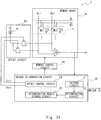
- Fig. 1 is a block diagram showing a semiconductor device according to the first embodiment.
- a semiconductor device 1 according to this embodiment includes a memory array 10, a unique ID generation circuit 20, an offset circuit 30, and a memory control circuit 40.
- the memory array 10 includes a plurality of complementary cells 11, each of the complementary cells 11 including a memory cell MC1 and a memory cell MC2. Each of the complementary cells 11 is configured to be able to hold data using the difference between a threshold voltage Vt1 of the memory cell MC1 and a threshold voltage Vt2 of the memory cell MC2.
- Fig. 2 is a diagram showing a configuration example of the memory cells MC1 and MC2 used in the semiconductor device according to this embodiment.
- each of the memory cells MC1 and MC2 includes a source region S, a drain region D, a channel forming region 15 provided between the source region S and the drain region D, and a control gate CG and a memory gate MG arranged on the channel forming region 15 with a gate insulating film 16 interposed therebetween.
- a charge trapping region 17 such as silicon nitride is arranged between the memory gate MG and the gate insulating film 16.
- the memory cells MC1 and MC2 are split gate flash memory cells (e.g., SG-MONOS).
- the drain regions D of the respective memory cells MC1 and MC2 are connected to bit lines BL1 and BL2, the source regions S thereof are connected to a source line SL, the control gates CG are connected to a word line WL, and the memory gates MG are connected to a memory gate selection line MGL.
- the threshold voltages Vt1 and Vt2 of the memory cells MC1 and MC2 vary depending on the number of electrons trapped by the charge trapping region 17 of the memory cells MC1 and MC2. Specifically, when the number of the electrons trapped by the charge trapping region 17 of the memory cells MC1 and MC2 is large, the threshold voltages Vt1 and Vt2 increase. On the other hand, when the number of the electrons trapped by the charge trapping region 17 of the memory cells MC1 and MC2 is small, the threshold voltages Vt1 and Vt2 decrease.
- V D 0 V
- V CG 1.5 V
- V MG 10 V
- V SL 6 V
- V D 0 V
- V CG 0 V
- V MG -10 V
- V SL 6 V.
- V D 1.5 V
- V CG 1.5 V
- V MG 0 V
- V SL 0 V.
- the threshold voltages Vt1 and Vt2 of the memory cells MC1 and MC2 are low, the memory cells MC1 and MC2 are in the ON state.
- the threshold voltages Vt1 and Vt2 of the memory cells MC1 and MC2 are high, the memory cells MC1 and MC2 are in the OFF state.
- the voltage values V D , V CG , V MG , and V SL of the memory cells MC1 and MC2 described above are merely examples, and values other than those stated above may be used in the semiconductor device according to this embodiment. Further, the configuration of the memory cells MC1 and MC2 shown in Fig. 2 is merely one example, and a memory cell having a configuration other than that shown in Fig. 2 may be used in the semiconductor device according to this embodiment.
- Figs. 3A to 3C are a diagram showing a distribution of the threshold voltages Vt1 and Vt2 of the memory cells MC1 and MC2 that form the complementary cell 11.
- the complementary cell 11 is configured to be able to hold data using the difference between the threshold voltage Vt1 of the memory cell MC1 and the threshold voltage Vt2 of the memory cell MC2.
- the complementary cell 11 is configured to be able to hold data using the two-bit memory cells MC1 and MC2.
- the memory cell MC1 may be herein referred to as a "positive memory” and the memory cell MC2 may be herein referred to as a "negative memory”.
- the relation between the threshold voltages Vt1 and Vt2 of the memory cells MC1 and MC2 and the data in the complementary cell 11 may be defined in such a way that this relation becomes opposite to that in the case shown in Figs. 3A and 3B . That is, when the threshold voltage Vt1 of the memory cell MC1 is higher than the threshold voltage Vt2 of the memory cell MC2, data “1" may be written in the complementary cell 11. Further, when the threshold voltage Vt2 of the memory cell MC2 is higher than the threshold voltage Vt1 of the memory cell MC1, data "0" may be written in the complementary cell 11.
- the aforementioned state of the threshold voltages Vt1 and Vt2 of the memory cells MC1 and MC2 can be read out using a sense amplifier SA provided in the memory array 10. Further, the data writing to the memory cells MC1 and MC2 and the data reading from the memory cells MC1 and MC2 described above can be executed using the memory control circuit 40. Specifically, by controlling the bit lines BL1 and BL2, the word line WL, the memory gate selection line MGL, the source line SL and the like of the memory cell array 10 using the memory control circuit 40, the data writing to the memory cells MC1 and MC2 and the data reading from the memory cells MC1 and MC2 can be executed.
- Fig. 3C shows a distribution of the threshold voltages Vt1 and Vt2 of the memory cells MC1 and MC2 in the initial state after the memory array 10 is manufactured. As shown in Fig. 3C , in the initial state, the distributions of the threshold voltages Vt1 and Vt2 of the memory cells MC1 and MC2 overlap each other, and the threshold voltages Vt1 and Vt2 uniformly vary. In the following description, the threshold voltages Vt1 and Vt2 of the memory cells MC1 and MC2 may be collectively referred to as a threshold voltage Vt.
- Fig. 4 is a diagram showing a relation between the initial threshold voltages Vt of the memory cells MC1 and MC2 and a cumulative probability. As shown in Fig. 4 , the initial threshold voltages Vt of the memory cells MC1 and MC2 uniformly varies. Therefore, when the memory cells MC1 and MC2 are randomly retrieved to examine the threshold voltages Vt1 and Vt2, there may be a difference between the threshold voltage Vt1 and the threshold voltage Vt2.
- the initial threshold voltage Vt1 of the memory cell MC1 when there is a potential difference ⁇ V between the initial threshold voltage Vt1 of the memory cell MC1 and the initial threshold voltage Vt2 of the memory cell MC2, it is possible to read out predetermined data ("1" or "0") by carrying out processing of reading out data by connecting the memory cell MC1 and the memory cell MC2 to the sense amplifier SA.
- the initial threshold voltage Vt2 of the memory cell MC2 is higher than the initial threshold voltage Vt1 of the memory cell MC1. In this case, data "1" is read out.
- the ID specific to the memory array 10 can be generated.
- the potential difference ⁇ Vt between the initial threshold voltages Vt1 and Vt2 of the memory cells MC1 and MC2 needs to be equal to or larger than 0.5 V in Fig. 5 , about 0.763 ⁇ (22.3 %) of the memory cells cannot be used to generate the unique ID since the difference between the initial threshold voltages Vt1 and Vt2 of the memory cells MC1 and MC2 is small and the data that has been read out becomes indefinite.
- the potential difference ⁇ Vt between the threshold voltages to be required is set to be equal to or larger than 0.5 V, about 75 % of all the memory cells can be used to generate the unique ID.
- Fig. 6 is a diagram showing a relation between the potential difference ⁇ Vt between the initial threshold voltages Vt1 and Vt2 and the cumulative probability.
- e.g., 0.5 V
- becomes smaller than the predetermined value of
- the data in these memory cells are read out, the data becomes unstable (indefinite) and the error rate increases when the unique ID is generated.
- the unique ID generation circuit 20 shown in Fig. 1 uses the unique ID generation circuit 20 shown in Fig. 1 , these unstable memory cells (bits) are specified, and these memory cells are masked so that these cells are not used when the unique ID is generated.
- the unique ID is generated by extracting only the memory cells having ⁇ Vt equal to or larger than a minimum sensitivity of the sense amplifier SA. It is therefore possible to improve the reliability of the unique ID that has been generated.
- the unique ID generation circuit 20 will be explained.
- the unique ID generation circuit 20 shown in Fig. 1 generates the ID specific to the memory array 10 using the initial threshold voltage Vt1 of the memory cell MC1 and the initial threshold voltage Vt2 of the memory cell MC2.
- the unique ID generation circuit 20 reads data (first data) in the complementary cell 11 in a first state in which the initial threshold voltage Vt1 of the memory cell MC1 has been virtually offset and reads data (second data) in the complementary cell 11 in a second state in which the initial threshold voltage Vt2 of the memory cell MC2 has been virtually offset.
- the data (the first data) in the complementary cell 11 read out in the first state coincides with the data (the second data) in the complementary cell 11 read out in the second state, the data in the complementary cell 11 is used as the unique ID.
- the unique ID generation circuit 20 includes a holding circuit 21, a determination circuit 22, a determination result storage circuit 23, and an offset control circuit 24.
- the holding circuit 21 temporarily holds the data read out from the memory array 10 when the unique ID is generated, that is, the data output from the sense amplifier SA. Specifically, the holding circuit 21 temporarily holds the data (the first data) in the complementary cell 11 read out in the first state in which the initial threshold voltage Vt1 of the memory cell MC1 has been virtually offset and the data (the second data) in the complementary cell 11 read out in the second state in which the initial threshold voltage Vt2 of the memory cell MC2 has been virtually offset.
- the determination circuit 22 receives the data (the first data) in the complementary cell 11 that has been read out in the first state and has been held in the holding circuit 21 and the data (the second data) in the complementary cell 11 that has been read out in the second state and has been held in the holding circuit 21, and determines whether these data coincide with each other.
- the determination result storage circuit 23 stores the results of the determination in the determination circuit 22.
- the determination result storage circuit 23 may store address information on the complementary cell 11 in which the data in the complementary cell 11 read out in the first state and the data in the complementary cell 11 read out in the second state have not coincided with each other.
- the unique ID generation circuit 20 is able to generate the unique ID without using the complementary cell 11 that corresponds to the address information stored in the determination result storage circuit 23 (i.e., the unstable complementary cell with a low reliability) when the next unique ID is generated.
- the determination result storage circuit 23 may store the address information on the complementary cell 11 in which the data in the complementary cell 11 read out in the first state and the data in the complementary cell 11 read out in the second state have coincided with each other.
- the unique ID generation circuit 20 is able to generate the unique ID using the complementary cell 11 that corresponds to the address information stored in the determination result storage circuit 23 (i.e., the stable complementary cell with a high reliability) when the next unique ID is generated.
- the offset control circuit 24 controls the offset circuit 30 to virtually reduce the initial threshold voltage Vt1 of the memory cell MC1. In a similar way, the offset control circuit 24 controls the offset circuit 30 to virtually reduce the initial threshold voltage Vt2 of the memory cell MC2.
- the offset circuit 30 is composed of transistors Tr1 and Tr2.
- the transistor Tr1 is connected between the bit line BL1 of the memory array 10 and the ground potential, and includes a gate to which an offset control signal Ctr1 is supplied from the offset control circuit 24.
- the transistor Tr1 is switched to the ON state when it is supplied with a high-level offset control signal Ctr1 from the offset control circuit 24.
- the bit line BL1 is electrically connected to the ground potential via the transistor Tr1. Therefore, the current is drawn out from the bit line BL1, and the initial threshold voltage Vt1 of the memory cell MC1 is virtually reduced.
- the transistor Tr2 is connected between the bit line BL2 of the memory array 10 and the ground potential, and includes a gate to which an offset control signal Ctr2 is supplied from the offset control circuit 24.
- the transistor Tr2 is switched to the ON state when it is supplied with a high-level offset control signal Ctr2 from the offset control circuit 24.
- the bit line BL2 is electrically connected to the ground potential via the transistor Tr2. Therefore, the current is drawn out from the bit line BL2, and the initial threshold voltage Vt2 of the memory cell MC2 is virtually reduced.
- the transistors Tr1 and Tr2 serve as current drawing circuits.
- the unique ID generation circuit 20 first switches on the transistor Tr1 and switches off the transistor Tr2.
- the transistor Tr1 When the transistor Tr1 is turned on, the current is drawn out from the bit line BL1 and the initial threshold voltage Vt1 of the memory cell MC1 is virtually reduced.
- the transistor Tr1 is switched to the OFF state and the transistor Tr2 is switched to the ON state.
- the transistor Tr2 When the transistor Tr2 is turned on, the current is drawn out from the bit line BL2, and the initial threshold voltage Vt2 of the memory cell MC2 is virtually reduced.
- the data (the second data) in the complementary cell 11 is read out.
- the first data in the complementary cell 11 read out in the first state coincides with the second data in the complementary cell 11 read out in the second state, the data in the complementary cell 11 is used as the unique ID.
- Fig. 7 is a diagram showing a relation between the initial threshold voltages Vt1 and Vt2 of the memory cells MC1 and MC2 included in each of complementary cells #1-#5 and the data that has been read out.
- the white circle and the black circle in each of the complementary cells #1-#5 in Fig. 7 respectively indicate the values of the threshold voltages Vt1 and Vt2 of the memory cells MC1 and MC2 that form the complementary cells #1-#5.
- the white circle (p) indicates the value of the threshold voltage Vt1 of the memory cell MC1 (positive memory)
- the black circle (n) indicates the value of the threshold voltage Vt2 of the memory cell MC2 (negative memory).
- Fig. 7 shows that the values of the threshold voltages Vt1 and Vt2 become larger as the white circle and the black circle go upward.
- the complementary cell #1 a case in which the threshold voltages Vt1 and Vt2 of the memory cells MC1 and MC2 have substantially the same value is shown.
- the complementary cells #2 and #3 a case in which, while there is a difference between the values of the threshold voltages Vt1 and Vt2 of the memory cells MC1 and MC2, the potential difference ⁇ Vt between them is small is shown.
- the complementary cells #4 and #5 a case in which the potential difference ⁇ Vt between the threshold voltages Vt1 and Vt2 of the memory cells MC1 and MC2 is large is shown.
- the threshold voltages Vt1 and Vt2 of the memory cells MC1 and MC2 are substantially the same value. Therefore, the data that has been read out in the first reading and the data that has been read out in the second reading are inverted from each other. From the discussion above, when the unique ID is generated using the complementary cell in which the potential difference ⁇ Vt between the threshold voltages Vt1 and Vt2 is small, the resulting data becomes unstable (indefinite), and the error rate increases when the unique ID is generated.
- the memory cells (bits) that tend to be unstable (indefinite) are specified and these memory cells are masked so that these masks are not used to generate the unique ID.
- the unique ID generation method an operation of the semiconductor device according to this embodiment (the unique ID generation method) will be explained in detail with reference to Figs. 8 and 9 .
- Fig. 8 is a diagram for describing an operation of the semiconductor device according to this embodiment.
- Fig. 9 is a flowchart for describing the operation of the semiconductor device according to this embodiment. Note that the initial threshold voltages Vt1 and Vt2 of the memory cells MC1 and MC2 in each of the complementary cells #1-#5 shown in Fig. 8 are similar to the initial threshold voltages Vt1 and Vt2 of the memory cells MC1 and MC2 in each of the complementary cells #1-#5 shown in Fig. 7 .
- the initial threshold voltage Vt1 of the memory cell MC1 of each of the complementary cells #1-#5 is offset (Step S1 in Fig. 9 ).
- the offset control circuit 24 shown in Fig. 1 supplies the high-level offset control signal Ctr1 to the gate of the transistor Tr1 and the low-level offset control signal Ctr2 to the gate of the transistor Tr2. Accordingly, the transistor Tr1 is switched to the ON state and the transistor Tr2 is switched to the OFF state.
- the transistor Tr1 is turned on, the bit line BL1 is electrically connected to the ground potential via the transistor Tr1, the current is drawn out from the bit line BL1, and the initial threshold voltage Vt1 of the memory cell MC1 is virtually reduced.
- the unique ID generation circuit 20 shown in Fig. 1 sends an instruction to the memory control circuit 40 to cause the memory control circuit 40 to execute a reading operation to the memory cell array 10.
- the memory control circuit 40 receives the instruction from the unique ID generation circuit 20, it executes the reading operation to the memory cell array 10.
- the data (the first data) in each of the complementary cells #1-#5 is output from the sense amplifier SA.
- This output data (the first data) is temporarily held in the holding circuit 21 (Step S3 in Fig. 9 ) .
- the initial threshold voltage Vt2 of the memory cell MC2 of each of the complementary cells #1-#5 is offset (Step S4 in Fig. 9 ).
- the offset control circuit 24 shown in Fig. 1 supplies the low-level offset control signal Ctr1 to the gate of the transistor Tr1 and the high-level offset control signal Ctr2 to the gate of the transistor Tr2. Accordingly, the transistor Tr1 is switched to the OFF state and the transistor Tr2 is switched to the ON state.
- the transistor Tr2 is turned on, the bit line BL2 is electrically connected to the ground potential via the transistor Tr2, the current is drawn out from the bit line BL2, and the initial threshold voltage Vt2 of the memory cell MC2 is virtually reduced.
- Step S5 in Fig. 9 When the data (the second data) in the complementary cells #1-#5 is read out in this state (Step S5 in Fig. 9 ), as shown in (b) in Fig. 8 , the data in the complementary cell #1 becomes “1", the data in the complementary cell #2 becomes “1”, the data in the complementary cell #3 becomes “1”, the data in the complementary cell #4 becomes “1", and the data in the complementary cell #5 becomes "0".
- the data (the second data) in each of the complementary cells #1-#5 is output from the sense amplifier SA.
- This output data (the second data) is temporarily held in the holding circuit 21 (Step S6 in Fig. 9 ).
- the determination circuit 22 shown in Fig. 1 receives the first and second data held in the holding circuit 21 and compares whether these data coincide with each other for each bit (Step S7 in Fig. 9 ). When the first and second data coincide with each other, the determination circuit 22 determines that the complementary cell in which the first and second data coincide with each other is the stable complementary cell (the stable bit) (Step S8). The data read out from the complementary cell determined to be the stable complementary cell in Step S8 is used as the unique ID (Step S9) .
- the determination circuit 22 determines that this complementary cell is the unstable complementary cell (the unstable bit) (Step S10).
- the determination result storage circuit 23 shown in Fig. 1 stores the address information on the complementary cell that has been determined to be the unstable complementary cell in Step S10 (Step S11).
- the unique ID generation circuit 20 is able to generate the unique ID without using the complementary cell 11 that corresponds to the address information stored in the determination result storage circuit 23 (i.e., the unstable complementary cell with a low reliability) when the next unique ID is generated.
- the complementary cells #1-#3 in the complementary cells #1-#3, the data (the first data) read out in the state in which the threshold voltage Vt1 of the memory cell MC1 is virtually offset and the data (the second data) read out in the state in which the threshold voltage Vt2 of the memory cell MC2 is virtually offset are inverted from each other (i.e., indefinite: X). Accordingly, in the complementary cells #1-#3, since the potential difference ⁇ Vt between the threshold voltage Vt1 of the memory cell MC1 and the threshold voltage Vt2 of the memory cell MC2 is small, it can be said that this cell is too unstable to be used as the unique ID.
- the complementary cells #4 and #5 the data (the first data) read out in the state in which the threshold voltage Vt1 of the memory cell MC1 is virtually offset and the data (the second data) read out in the state in which the threshold voltage Vt2 of the memory cell MC2 is virtually offset coincide with each other. Accordingly, in the complementary cells #4 and #5, since the potential difference ⁇ Vt between the threshold voltage Vt1 of the memory cell MC1 and the threshold voltage Vt2 of the memory cell MC2 is large, this cell can be used as the highly reliable unique ID.
- the determination result storage circuit 23 shown in Fig. 1 may store the address information on the complementary cell determined to be the stable complementary cell instead of storing the address information on the complementary cell determined to be the unstable complementary cell.
- the unique ID generation circuit 20 is able to generate the unique ID using the complementary cell 11 that corresponds to the address information stored in the determination result storage circuit 23 (i.e., the stable complementary cell with a high reliability) when the next unique ID is generated.
- Fig. 10 is a diagram showing a relation between an error probability and the cumulative probability when the data in the complementary cell is read out.
- the data in the complementary cell composed of the memory cells MC1 and MC2 (the initial threshold voltages Vt1 and Vt2) is read out in the normal method, a reading error occurs with a certain probability. Therefore, when the unique ID generation method according to this embodiment is not used, the reliability of the unique ID that has been generated is reduced.
- the symbols (a)-(c) in Fig. 10 correspond to (a)-(c) shown in Fig. 8 . That is, (a) in Fig. 10 indicates the error probability when the data in the complementary cell has been read out in the state in which the initial threshold voltage Vt1 of the memory cell MC1 is offset. Further, (b) in Fig. 10 indicates the error probability when the data in the complementary cell has been read out in the state in which the initial threshold voltage Vt2 of the memory cell MC2 is offset. Further, (c) in Fig. 10 indicates the error probability after the unstable complementary cell (indefinite bit) is masked. The symbol (d) in Fig. 10 corresponds to the value obtained by adding the error probability shown in (a) in Fig. 10 and the error probability shown in (b) in Fig. 10 .
- the error probability after the unstable complementary cell (indefinite bit) is masked is lower than the error probability in the case in which the normal reading is performed. Accordingly, by masking the unstable complementary cell using the unique ID generation method according to this embodiment, it is possible to improve the reliability of the unique ID that has been generated.
- Fig. 11 is a diagram for describing an address space 50 of the memory array 10 included in the semiconductor device 1 according to this embodiment. As shown in Fig. 11 , a user region 51 and an extra region 52 are provided in the address space 50 of the memory array 10. In this embodiment, by using a part of the extra region 52 as a region to obtain the initial threshold voltage Vt, a security function can be added without changing the general memory array 10 (flash memory).
- a complementary cell arranged in the address space of the user region 51 may be used as a complementary cell for data holding and a complementary cell arranged in the address space of the extra region 52 may be used as a complementary cell for unique ID generation.
- the memory control circuit 40 shown in Fig. 1 may switch, when the first and second data read out from the complementary cell have not coincided with each other (i.e., when this complementary cell has been determined to be the unstable complementary cell), the complementary cell in which the first and second data have not coincided with each other from the complementary cell for unique ID generation to the complementary cell for data holding. That is, as shown in Fig. 12 , when the complementary cell arranged in the address space of the extra region 52 is determined to be the unstable complementary cell when it is used as the complementary cell for unique ID generation, this unstable complementary cell may be switched to the complementary cell for data holding (the address space of the complementary cell is indicated by a symbol 53). According to this configuration, the unstable complementary cell can be efficiently used.
- Fig. 13 is a block diagram showing another configuration example of the semiconductor device according to this embodiment.
- the configuration of an offset circuit 60 in the semiconductor device 2 shown in Fig. 13 is different from that in the semiconductor device 1 shown in Fig. 1 . Since the configurations other than those stated above are similar to those of the semiconductor device 1 shown in Fig. 1 , the same components are denoted by the same reference symbols and overlapping descriptions will be omitted.
- the offset control circuit 24 controls the offset circuit 60 to virtually increase the initial threshold voltage Vt1 of the memory cell MC1. In a similar way, the offset control circuit 24 controls the offset circuit 60 to virtually increase the initial threshold voltage Vt2 of the memory cell MC2.
- the offset circuit 60 is composed of transistors Tr11 and Tr12 and a constant current source 61.
- the transistor Tr11 is connected between the bit line BL1 of the memory array 10 and the constant current source 61, and includes a gate to which the offset control signal Ctr1 is supplied from the offset control circuit 24.
- the transistor Tr11 is turned on when the high-level offset control signal Ctr1 is supplied from the offset control circuit 24.
- the bit line BL1 is electrically connected to the constant current source 61 via the transistor Tr11. Therefore, the current is supplied to the bit line BL1 and the initial threshold voltage Vt1 of the memory cell MC1 is virtually increased.
- the transistor Tr12 is connected between the bit line BL2 of the memory array 10 and the constant current source 61, and includes a gate to which the offset control signal Ctr2 is supplied from the offset control circuit 24.
- the transistor Tr12 is turned on when it is supplied with the high-level offset control signal Ctr2 from the offset control circuit 24.
- the bit line BL2 is electrically connected to the constant current source 61 via the transistor Tr12. Therefore, the current is supplied to the bit line BL2 and the initial threshold voltage Vt2 of the memory cell MC2 is virtually increased.
- the transistors Tr11 and Tr12 serve as current supply circuits.
- the unique ID generation circuit 20 first turns on the transistor Tr11 and turns off the transistor Tr12.
- the transistor Tr11 When the transistor Tr11 is turned on, the current is supplied to the bit line BL1 and the initial threshold voltage Vt1 of the memory cell MC1 is virtually increased.
- the transistor Tr11 is switched to the OFF state and the transistor Tr12 is switched to the ON state.
- the transistor Tr12 When the transistor Tr12 is turned on, the current is supplied to the bit line BL2 and the initial threshold voltage Vt2 of the memory cell MC2 is virtually increased.
- the data (the second data) in the complementary cell 11 is read out.
- the first data in the complementary cell 11 read out in the first state coincides with the second data in the complementary cell 11 read out in the second state, the data in the complementary cell 11 is used as the unique ID.
- the unique ID generation circuit 20 by using the unique ID generation circuit 20, the memory cells (bits) that tend to be unstable (indefinite) are specified and these memory cells are masked so that these masks are not used to generate the unique ID.
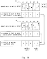
- Fig. 14 is a diagram for describing an operation of the semiconductor device according to this embodiment, and corresponds to the diagram shown in Fig. 8 .
- the initial threshold voltage Vt1 of the memory cell MC1 of each of the complementary cells #1-#5 is offset.
- the offset control circuit 24 shown in Fig. 13 supplies the high-level offset control signal Ctr1 to the gate of the transistor Tr11 and the low-level offset control signal Ctr2 to the gate of the transistor Tr12. Accordingly, the transistor Tr11 is switched to the ON state and the transistor Tr12 is switched to the OFF state.
- the transistor Tr11 is turned on, the bit line BL1 is connected to the constant current source 61 via the transistor Tr1, the current is supplied to the bit line BL1, and the initial threshold voltage Vt1 of the memory cell MC1 is virtually increased.
- the data (the first data) in each of the complementary cells #1-#5 is output from the sense amplifier SA.
- This output data (the first data) is temporarily held in the holding circuit 21.
- the initial threshold voltage Vt2 of the memory cell MC2 of each of the complementary cells #1-#5 is offset.
- the offset control circuit 24 shown in Fig. 13 supplies the low-level offset control signal Ctr1 to the gate of the transistor Tr11 and supplies the high-level offset control signal Ctr2 to the gate of the transistor Tr12. Accordingly, the transistor Tr11 is switched off and the transistor Tr12 is switched on.
- the bit line BL2 is electrically connected to the constant current source 61 via the transistor Tr12, the current is supplied to the bit line BL2, and the initial threshold voltage Vt2 of the memory cell MC2 is virtually increased.
- the data (the second data) in each of the complementary cells #1-#5 is output from the sense amplifier SA.
- This output data (the second data) is temporarily held in the holding circuit 21.
- the determination circuit 22 shown in Fig. 13 receives the first and second data held in the holding circuit 21, and compares whether these data coincide with each other for each bit. When the first data and the second data coincide with each other, the determination circuit 22 determines that the complementary cell in which the first and second data coincide with each other is the stable complementary cell (the stable bit). The data read out from the complementary cell that has been determined to be the stable complementary cell is used as the unique ID.
- the determination circuit 22 determines that this complementary cell is the unstable complementary cell (the unstable bit).
- the determination result storage circuit 23 shown in Fig. 13 stores the address information on the complementary cell that has been determined to be the unstable complementary cell.
- the unique ID generation circuit 20 is able to generate the unique ID without using the complementary cell 11 that corresponds to the address information stored in the determination result storage circuit 23 (i.e., the unstable complementary cell with a low reliability) when the next unique ID is generated.
- the complementary cells #1-#3 in the complementary cells #1-#3, the data (the first data) read out in the state in which the threshold voltage Vt1 of the memory cell MC1 is virtually offset and the data (the second data) read out in the state in which the threshold voltage Vt2 of the memory cell MC2 is virtually offset are inverted from each other (i.e., indefinite: X). Accordingly, in the complementary cells #1-#3, since the potential difference ⁇ Vt between the threshold voltage Vt1 of the memory cell MC1 and the threshold voltage Vt2 of the memory cell MC2 is small, it can be said that these cells are too unstable to be used as the unique ID.
- the complementary cells #4 and #5 the data (the first data) read out in the state in which the threshold voltage Vt1 of the memory cell MC1 is virtually offset and the data (the second data) read out in the state in which the threshold voltage Vt2 of the memory cell MC2 is virtually offset coincide with each other. Accordingly, in the complementary cells #4 and #5, since the potential difference ⁇ Vt between the threshold voltage Vt1 of the memory cell MC1 and the threshold voltage Vt2 of the memory cell MC2 is large, these cells can be used as highly reliable unique IDs.
- a semiconductor device is different from the semiconductor device described in the first embodiment in that the proportion of the complementary cells that are determined to be the unstable complementary cells (memory cells) in the unique ID generation circuit 20 is made smaller than a predetermined proportion. Since the other configurations are similar to those of the semiconductor device described in the first embodiment, overlapping descriptions thereof will be omitted as appropriate.
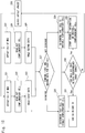
- Fig. 15 is a flowchart for describing an operation of the semiconductor device according to this embodiment.
- the operations in Steps S21-S27 are similar to those of Steps S1-S7 in the flowchart shown in Fig. 9 . Therefore, overlapping descriptions will be omitted.
- Step S27 shown in Fig. 15 the determination circuit 22 included in the unique ID generation circuit 20 compares whether the first and second data held in the holding circuit 21 coincide with each other for each bit. When the first and second data coincide with each other, the determination circuit 22 determines that the complementary cell in which the first and second data coincide with each other is the stable complementary cell (the stable bit) (Step S28). On the other hand, when the first and second data do not coincide with each other, the determination circuit 22 determines that this complementary cell is the unstable complementary cell (the unstable bit) (Step S29).
- the determination circuit 22 determines whether the proportion of the complementary cells in which the first and second data do not coincide with each other (the unstable bit rate) with respect to the complementary cells in which the first and second data coincide with each other falls within a predetermined target range (Step S30).
- the "predetermined target range” is a target value of the proportion of the complementary cells masked by the unique ID generation circuit 20, and is a range having a predetermined width.
- This target range is a range in which the unique ID can be retrieved from the semiconductor device in a stable manner, and is determined in consideration of the temperature under which the semiconductor device is used, the voltage fluctuation, reading after a long retention time, etc. That is, while it is assumed that the unique ID can be retrieved in a stable manner, the target value of the unstable bit is determined in advance and the target range is determined.
- the data read out from the complementary cell determined to be the stable complementary cell in Step S28 is used as the unique ID (Step S31).
- the determination result storage circuit 23 shown in Fig. 1 stores the address information on the complementary cell that has been determined to be the unstable complementary cell in Step S29 (Step S32).
- the unique ID generation circuit 20 is able to generate the unique ID without using the complementary cell 11 that corresponds to the address information stored in the determination result storage circuit 23 (i.e., the unstable complementary cell with a low reliability) when the next unique ID is generated.
- the unique ID generation circuit 20 adjusts the absolute value of the offset amount when the initial threshold voltages of the memory cells MC1 and MC2 have been virtually offset (Step S33) .
- the unique ID generation circuit 20 reduces the absolute value of the offset amount when the initial threshold voltages Vt1 and Vt2 of the memory cells MC1 and MC2 are virtually offset. Accordingly, the conditions when the complementary cell is masked are relieved and the number of unstable complementary cells (the unstable bits) masked by the unique ID generation circuit 20 can be reduced. Accordingly, it is possible to prevent the unique ID generation circuit 20 from masking the complementary cells more than necessary.
- the voltage supplied to the gate of each of the transistors Tr1 and Tr2 is reduced. It is therefore possible to reduce the amount of the current drawn out from the bit lines BL1 and BL2 and to reduce the offset amount of the initial threshold voltages Vt1 and Vt2 of the memory cells MC1 and MC2.
- the voltage supplied to the gate of each of the transistors Tr11 and Tr12 is reduced. Accordingly, it is possible to reduce the amount of the current supplied to the bit lines BL1 and BL2 from the constant current source 61, thereby reducing the offset amount of the initial threshold voltages Vt1 and Vt2 of the memory cells MC1 and MC2.
- the unique ID generation circuit 20 increases the absolute value of the offset amount when the initial threshold voltages Vt1 and Vt2 of the memory cells MC1 and MC2 are virtually offset. Accordingly, the conditions when the complementary cells are masked become severe, and the number of unstable complementary cells (the unstable bits) masked by the unique ID generation circuit 20 can be increased. Accordingly, the reliability of the unique ID generated in the unique ID generation circuit 20 can be improved.
- the voltage supplied to the gate of each of the transistors Tr1 and Tr2 is increased. It is therefore possible to increase the amount of the current drawn out from the bit lines BL1 and BL2, whereby it is possible to increase the offset amount of the initial threshold voltages Vt1 and Vt2 of the memory cells MC1 and MC2.
- the voltage supplied to the gate of each of the transistors Tr11 and Tr12 is increased. Accordingly, it is possible to increase the amount of the current supplied to the bit lines BL1 and BL2 from the constant current source 61, whereby it is possible to increase the offset amount of the initial threshold voltages Vt1 and Vt2 of the memory cells MC1 and MC2.
- the proportion of the complementary cells to be masked can be set within a predetermined target range. Accordingly, it is possible to optimize the proportion of the complementary cells to be masked. Accordingly, it is possible to prevent the complementary cells from being masked more than necessary while improving the reliability of the unique ID to be generated. It is therefore possible to efficiently generate the unique ID.
- Figs. 16A and 16B are diagrams showing changes in the potential of the bit line with time.
- the initial threshold voltage Vt of the memory cell when the initial threshold voltage Vt of the memory cell is too high, the amount of the current that flows between the source and the drain of the memory cell is small. In this case, after the bit line is precharged, the potential of the bit line is gradually reduced. Therefore, when, for example, the potential difference between the bit lines BL1 and BL2 is detected at the sense timing shown in Fig. 16A , the data in the complementary cell may be indefinite since the potential difference between the bit lines is small.
- the semiconductor device capable of masking the unstable complementary cell (the unstable bit) even when the initial threshold voltage Vt is outside the appropriate range.
- two methods (1) a method of adjusting the voltage level of the memory gate MG and (2) a method of adjusting the sense timing, will be explained. Since the other configurations are similar to those of the semiconductor devices described in the first and second embodiments, overlapping descriptions will be omitted as appropriate.
- the threshold voltage Vt of the memory cell can be adjusted. Specifically, the property of the threshold voltage Vt that it is reduced as the voltage V MG applied to the memory gate MG becomes higher and it is increased as the voltage V MG applied to the memory gate MG becomes lower is used.
- the unique ID generation circuit 20 shown in Fig. 1 adjusts the voltage V MG applied to the memory gate MG
- the unique ID generation circuit 20 sends an instruction to the memory control circuit 40 to cause the memory control circuit 40 to adjust the voltage V MG of the memory gate MG.
- the memory control circuit 40 receives the instruction to adjust the voltage V MG of the memory gate MG from the unique ID generation circuit 20, the memory control circuit 40 applies a predetermined voltage V MG to the memory gate MG of the memory cell array 10.
- Fig. 17 is a flowchart for describing one example of operations of the semiconductor device according to this embodiment.
- the value of the initial threshold voltage Vt is unknown. Therefore, in this embodiment, as shown in Fig. 17 , the unstable bit detection processing described in the first embodiment (specifically, the processing of Steps S1-S7 shown in Fig. 9 ) is executed on the memory cell that has been manufactured (Step S41).
- Step S42 It is then determined whether the proportion of the unstable complementary cells (the unstable bit rate) falls within the predetermined target range (Step S42). When the proportion of the unstable complementary cells (the unstable bit rate) falls within the predetermined target range (Step S42: Yes), the processing shown in Fig. 17 is ended.
- the unique ID generation circuit 20 increases the voltage V MG of the memory gate MG (Step S43).
- Step S44 the unstable bit detection processing described in the first embodiment (specifically, the processing of Steps S1-S7 shown in Fig. 9 ) is executed again (Step S44).
- Step S45 It is then determined whether the proportion of the unstable complementary cells (the unstable bit rate) falls within the predetermined target range (Step S45).
- the processing shown in Fig. 17 is ended.
- the unique ID generation circuit 20 stores the voltage V MG of the memory gate MG at this time. In the following process, when the unique ID is generated, this voltage V MG that has been stored is applied to the memory gate MG to generate the unique ID.
- Step S45 when the proportion of the unstable complementary cells (the unstable bit rate) does not fall within the predetermined target range (Step S45: No), the unique ID generation circuit 20 reduces the voltage V MG of the memory gate MG (Step S46). After that, the unstable bit detection processing described in the first embodiment (specifically, processing of Steps S1-S7 shown in Fig. 9 ) is executed again (Step S41).
- Step S42 It is then determined whether the proportion of the unstable complementary cells (the unstable bit rate) falls within the predetermined target range (Step S42).
- the processing shown in Fig. 17 is ended.
- the unique ID generation circuit 20 stores the voltage V MG of the memory gate MG at this time. In the following process, when the unique ID is generated, this voltage V MG that has been stored is applied to the memory gate MG to generate the unique ID.
- Step S42 when the proportion of the unstable complementary cells (the unstable bit rate) does not fall within the predetermined target range (Step S42: No), the unique ID generation circuit 20 again increases the voltage V MG of the memory gate MG (Step S43). After that, the processing of Steps S41-S46 in Fig. 17 (i.e., the increase/decrease in the voltage V MG of the memory gate MG) is repeated until that the proportion of the unstable complementary cells (the unstable bit rate) falls within the predetermined target range.
- Step S43 the voltage V MG of the memory gate MG is reduced in Step S46 to check the change in the unstable bit rate.
- the voltage V MG of the memory gate MG is first increased and the voltage V MG of the memory gate MG is then reduced has been described.
- the voltage V MG of the memory gate MG may be reduced first and the voltage V MG of the memory gate MG may then be increased.
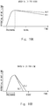
- the initial threshold voltage Vt of the memory cell is adjusted by adjusting the voltage V MG applied to the memory gate MG. Specifically, as shown in Fig. 18A , when the initial threshold voltage Vt of the memory cell is too high, the amount of the current that flows between the source and the drain of the memory cell is small. In this case, after the bit line is precharged, the potential of the bit line is gradually reduced (see dashed lines shown in Fig. 18A ). Therefore, when the potential difference between the bit lines BL1 and BL2 is detected at one sense timing, the data in the complementary cell may become indefinite since the potential difference between the bit lines is small.
- the initial threshold voltage Vt of the memory cell is adjusted to be low by increasing the voltage V MG applied to the memory gate MG (see solid lines in Fig. 18A ). Accordingly, the initial threshold voltage Vt of the memory cell can be adjusted to an appropriate range, whereby it is possible to suitably mask the unstable complementary cell (the unstable bit).
- the initial threshold voltage Vt of the memory cell is adjusted to become high by decreasing the voltage V MG applied to the memory gate MG (see solid lines in Fig. 18B ). Accordingly, the initial threshold voltage Vt of the memory cell can be adjusted to an appropriate range, whereby it is possible to suitably mask the unstable complementary cell (the unstable bit).
- the aforementioned processing is executed in advance before the unique ID generation processing is executed. Accordingly, even when the initial threshold voltage Vt of the memory cell is outside the appropriate range, it is possible to suitably mask the unstable complementary cell (the unstable bit).
- Fig. 19 is a flowchart for describing another example of the operation of the semiconductor device according to this embodiment.
- the value of the initial threshold voltage Vt is unknown. Therefore, in this embodiment, as shown in Fig. 19 , the unstable bit detection processing described in the first embodiment (specifically, the processing of Steps S1-S7 shown in Fig. 9 ) is executed first for the memory cell that has been manufactured (Step S51).
- Step S52 It is then determined whether the proportion of the unstable complementary cells (the unstable bit rate) is within the predetermined target range (Step S52). When the proportion of the unstable complementary cells (the unstable bit rate) falls within the predetermined target range (Step S52: Yes), the processing shown in Fig. 19 is ended.
- the unique ID generation circuit 20 delays the timing of reading the data in the complementary cell using the sense amplifier SA (Step S53).
- Step S54 the unstable bit detection processing described in the first embodiment (specifically, the processing of Steps S1-S7 shown in Fig. 9 ) is executed again (Step S54).
- the data in the complementary cell is read out at the timing set in Step S53, that is, by delaying the timing of reading out the data.
- Step S55 It is then determined whether the proportion of the unstable complementary cells (the unstable bit rate) falls within the predetermined target range (Step S55).
- the processing shown in Fig. 19 is ended.
- the unique ID generation circuit 20 stores the timing of reading the sense amplifier SA at this time, and generates the unique ID using the timing of reading the sense amplifier SA that has been stored when the next unique ID is generated.
- Step S55: No when the proportion of the unstable complementary cells (the unstable bit rate) does not fall within the predetermined target range (Step S55: No), the unique ID generation circuit 20 advances the timing of reading out the data in the complementary cell using the sense amplifier SA (Step S56). After that, the unstable bit detection processing described in the first embodiment (specifically, the processing of Steps S1-S7 shown in Fig. 9 ) is executed again (Step S51). In this case, the data in the complementary cell is read out at the timing set in Step S56, that is, by advancing the timing of reading out the data.
- Step S52 It is then determined whether the proportion of the unstable complementary cells (the unstable bit rate) falls within the predetermined target range (Step S52). When the proportion of the unstable complementary cells (the unstable bit rate) falls within the predetermined target range (Step S52: Yes), the processing shown in Fig. 19 is ended.
- the unique ID generation circuit 20 stores the timing of reading the sense amplifier SA at this time, and generates the unique ID using the timing of reading the sense amplifier SA that has been stored when the next unique ID is generated.
- Step S52 when the proportion of the unstable complementary cells (the unstable bit rate) does not fall within the predetermined target range (Step S52: No), the unique ID generation circuit 20 again delays the timing of reading out the data in the complementary cell using the sense amplifier SA (Step S53). After that, the processing of Steps S51-S56 in Fig. 19 (i.e., the processing of delaying the timing of reading the sense amplifier SA and the processing of advancing the same) is repeated until that the proportion of the unstable complementary cells (the unstable bit rate) falls within the predetermined target range.
- Step S53 the processing of delaying the timing of reading the sense amplifier SA is first executed in Step S53, the processing of advancing the timing of reading the sense amplifier SA is executed in Step S56 to check the change in the unstable bit rate.
- the timing of reading the sense amplifier SA is first delayed and the timing of reading the sense amplifier SA is then advanced has been described.
- the timing of reading the sense amplifier SA may be advanced first, and then the timing of reading the sense amplifier SA may be delayed.
- the initial threshold voltage Vt of the memory cell when the initial threshold voltage Vt of the memory cell is too high, the amount of the current that flows between the source and the drain of the memory cell is small. In this case, after the bit line is precharged, the potential of the bit line is gradually reduced. Therefore, when the potential difference between the bit lines BL1 and BL2 is detected at the sense timing shown by dashed lines in Fig. 20A , the data in the complementary cell may become indefinite since the potential difference between the bit lines is small. On the other hand, in this embodiment, as shown in solid lines of Fig. 20A , the timing of reading the sense amplifier SA is delayed. Accordingly, the potential difference between the bit lines detected by the sense amplifier SA becomes the potential difference with which the data can be read out, whereby it is possible to appropriately read out the data in the complementary cell.
- the aforementioned processing is executed in advance before the unique ID generation processing is executed. Accordingly, even when the initial threshold voltage Vt of the memory cell is outside the appropriate range, it is possible to suitably mask the unstable complementary cell (the unstable bit).
- the first to third embodiments can be combined as desirable by one of ordinary skill in the art.
Landscapes
- Engineering & Computer Science (AREA)
- Theoretical Computer Science (AREA)
- Computer Security & Cryptography (AREA)
- Physics & Mathematics (AREA)
- Microelectronics & Electronic Packaging (AREA)
- Computer Hardware Design (AREA)
- General Physics & Mathematics (AREA)
- General Engineering & Computer Science (AREA)
- Software Systems (AREA)
- Mathematical Physics (AREA)
- Computer Networks & Wireless Communication (AREA)
- Signal Processing (AREA)
- Read Only Memory (AREA)
Abstract
Description
- The present disclosure relates to a semiconductor device and a unique ID generation method, and relates to, for example, a semiconductor device and a unique ID generation method capable of generating an ID unique to a device using a PUF technology.
- In recent years, security technologies for protecting semiconductor devices such as microcomputers from unauthorized access have become important. One of these security technologies is a Physically Unclonable Function (PUF) technology. The PUF technology includes a technology of generating identifiers (IDs: identification) unique to semiconductor devices using manufacturing variations when the semiconductor devices are manufactured.
- Japanese Unexamined Patent Application Publication No.
2011-243263 - Japanese Unexamined Patent Application Publication No.
2016-105278 - When a unique ID is generated by applying the PUF technology to a non-volatile semiconductor memory disclosed in Japanese Unexamined Patent Application Publication No.
2011-243263 - However, since there is a variation between the initial threshold voltages of the memory cells MC1 and MC2, the difference between the initial threshold voltage of the memory cell MC1 and the initial threshold voltage of the memory cell MC2 may become small depending on the combination of the two memory cells MC1 and MC2. In this case, data read out from the complementary cell becomes unstable, which causes a problem that the reliability of the unique ID that has been generated is reduced.
- The other problems of the prior art and the novel characteristics of the present disclosure will be made apparent from the descriptions of the specification and the accompanying drawings.
- A semiconductor device according to one embodiment includes a unique ID generation circuit configured to generate a unique ID using a memory array including a plurality of complementary cells, each of the complementary cells includes first and second memory cells. The unique ID generation circuit uses, when data in the complementary cell read out in a first state in which an initial threshold voltage of the first memory cell has been virtually offset and data in the complementary cell read out in a second state in which an initial threshold voltage of the second memory cell has been virtually offset coincide with each other, the data in the complementary cell as the unique ID.
- According to the embodiment, it is possible to provide a semiconductor device and a unique ID generation method capable of improving the reliability of a unique ID that has been generated.
- The above and other aspects, advantages and features will be more apparent from the following description of certain embodiments taken in conjunction with the accompanying drawings, in which:
-
Fig. 1 is a block diagram showing a configuration example of a semiconductor device according to a first embodiment; -
Fig. 2 is a diagram showing a configuration example of a memory cell used in the semiconductor device according to the first embodiment; -
Figs. 3A to 3C are diagrams showing a distribution of threshold voltages Vt1 and Vt2 of memory cells MC1 and MC2 forming a complementary cell; -
Fig. 4 is a diagram showing a relation between initial threshold voltages Vt of the memory cells MC1 and MC2 and a cumulative probability; -
Fig. 5 is a diagram showing initial threshold voltages Vt1 and Vt2 of the memory cells MC1 and MC2; -
Fig. 6 is a diagram showing a relation between a difference (ΔVt) between the initial threshold voltages and the cumulative probability; -
Fig. 7 is a diagram showing a relation between the initial threshold voltages Vt1 and Vt2 of the memory cells MC1 and MC2 included in each of complementary cells #1-#5 and data that has been read out; -
Fig. 8 is a diagram for describing an operation of the semiconductor device according to the first embodiment; -
Fig. 9 is a flowchart for describing the operation of the semiconductor device according to the first embodiment; -
Fig. 10 is a diagram showing a relation between an error probability and a cumulative probability when data in the complementary cell is read out; -
Fig. 11 is a diagram for describing one example of an address space of a memory array included in the semiconductor device according to the first embodiment; -
Fig. 12 is a diagram for describing one example of the address space of the memory array included in the semiconductor device according to the first embodiment; -
Fig. 13 is a block diagram showing another configuration example of the semiconductor device according to the first embodiment; -
Fig. 14 is a diagram for describing an operation of the semiconductor device according to the first embodiment; -
Fig. 15 is a flowchart for describing an operation of a semiconductor device according to a second embodiment; -
Fig. 16A is a diagram showing changes in the potential of a bit line with time; -
Fig. 16B is a diagram showing changes in the potential of the bit line with time; -
Fig. 17 is a flowchart for describing one example of an operation of a semiconductor device according to a third embodiment; -
Fig. 18A is a diagram showing changes in the potential of a bit line with time; -
Fig. 18B is a diagram showing changes in the potential of the bit line with time; -
Fig. 19 is a flowchart for describing another example of the operation of the semiconductor device according to the third embodiment; -
Fig. 20A is a diagram showing changes in the potential of the bit line with time; and -
Fig. 20B is a diagram showing changes in the potential of the bit line with time. - Hereinafter, with reference to the drawings, a first embodiment will be explained.
-
Fig. 1 is a block diagram showing a semiconductor device according to the first embodiment. As shown inFig. 1 , asemiconductor device 1 according to this embodiment includes amemory array 10, a uniqueID generation circuit 20, anoffset circuit 30, and amemory control circuit 40. - The
memory array 10 includes a plurality ofcomplementary cells 11, each of thecomplementary cells 11 including a memory cell MC1 and a memory cell MC2. Each of thecomplementary cells 11 is configured to be able to hold data using the difference between a threshold voltage Vt1 of the memory cell MC1 and a threshold voltage Vt2 of the memory cell MC2. -
Fig. 2 is a diagram showing a configuration example of the memory cells MC1 and MC2 used in the semiconductor device according to this embodiment. As shown inFig. 2 , each of the memory cells MC1 and MC2 includes a source region S, a drain region D, achannel forming region 15 provided between the source region S and the drain region D, and a control gate CG and a memory gate MG arranged on thechannel forming region 15 with agate insulating film 16 interposed therebetween. Acharge trapping region 17 such as silicon nitride is arranged between the memory gate MG and thegate insulating film 16. As shown inFig. 2 , the memory cells MC1 and MC2 are split gate flash memory cells (e.g., SG-MONOS). - As shown in
Figs. 1 and2 , the drain regions D of the respective memory cells MC1 and MC2 are connected to bit lines BL1 and BL2, the source regions S thereof are connected to a source line SL, the control gates CG are connected to a word line WL, and the memory gates MG are connected to a memory gate selection line MGL. - In the configuration example of the memory cells MC1 and MC2 shown in
Fig. 2 , the threshold voltages Vt1 and Vt2 of the memory cells MC1 and MC2 vary depending on the number of electrons trapped by thecharge trapping region 17 of the memory cells MC1 and MC2. Specifically, when the number of the electrons trapped by thecharge trapping region 17 of the memory cells MC1 and MC2 is large, the threshold voltages Vt1 and Vt2 increase. On the other hand, when the number of the electrons trapped by thecharge trapping region 17 of the memory cells MC1 and MC2 is small, the threshold voltages Vt1 and Vt2 decrease. - In order to increase the threshold voltages Vt1 and Vt2 of the memory cells MC1 and MC2, for example, voltage values of the memory cells MC1 and MC2 are set to VD=0 V, VCG=1.5 V, VMG=10 V, and VSL=6 V. By setting the voltage values as stated above, a write current flows from the source region S to the drain region D, hot electrons that are generated in the boundary part between the control gate CG and the memory gate MG are injected into the
charge trapping region 17, and the threshold voltages Vt1 and Vt2 of the memory cells MC1 and MC2 increase. - On the other hand, in order to reduce the threshold voltages Vt1 and Vt2 of the memory cells MC1 and MC2, for example, the voltage values of the memory cells MC1 and MC2 are set to VD=0 V, VCG=0 V, VMG=-10 V, and VSL=6 V. By setting the voltage values as stated above, a high electric field is applied between the SL junction and the memory gate MG, and a hot hole is generated due to BtoB (Band-to-Band tunneling). This hot hole is injected into the
charge trapping region 17, and the threshold voltages Vt1 and Vt2 of the memory cells MC1 and MC2 are reduced. - Further, in order to read out data from the memory cells MC1 and MC2, for example, the voltage values of the memory cells MC1 and MC2 are set to VD=1.5 V, VCG=1.5 V, VMG=0 V, and VSL=0 V. In this case, when the threshold voltages Vt1 and Vt2 of the memory cells MC1 and MC2 are low, the memory cells MC1 and MC2 are in the ON state. On the other hand, when the threshold voltages Vt1 and Vt2 of the memory cells MC1 and MC2 are high, the memory cells MC1 and MC2 are in the OFF state.
- The voltage values VD, VCG, VMG, and VSL of the memory cells MC1 and MC2 described above are merely examples, and values other than those stated above may be used in the semiconductor device according to this embodiment. Further, the configuration of the memory cells MC1 and MC2 shown in
Fig. 2 is merely one example, and a memory cell having a configuration other than that shown inFig. 2 may be used in the semiconductor device according to this embodiment. -
Figs. 3A to 3C are a diagram showing a distribution of the threshold voltages Vt1 and Vt2 of the memory cells MC1 and MC2 that form thecomplementary cell 11. Thecomplementary cell 11 is configured to be able to hold data using the difference between the threshold voltage Vt1 of the memory cell MC1 and the threshold voltage Vt2 of the memory cell MC2. In other words, thecomplementary cell 11 is configured to be able to hold data using the two-bit memory cells MC1 and MC2. - For example, as shown in
Fig. 3A , when the threshold voltage Vt2 of the memory cell MC2 is higher than the threshold voltage Vt1 of the memory cell MC1, data "1" is written in thecomplementary cell 11. In other words, when the threshold voltage Vt1 of the memory cell MC1 is in the low level and the threshold voltage Vt2 of the memory cell MC2 is in the high level, data "1" is written to thecomplementary cell 11. - On the other hand, as shown in
Fig. 3B , when the threshold voltage Vt1 of the memory cell MC1 is higher than the threshold voltage Vt2 of the memory cell MC2, data "0" is written in thecomplementary cell 11. In other words, when the threshold voltage Vt1 of the memory cell MC1 is in the high level and the threshold voltage Vt2 of the memory cell MC2 is in the low level, data "0" is written in thecomplementary cell 11. - The memory cell MC1 may be herein referred to as a "positive memory" and the memory cell MC2 may be herein referred to as a "negative memory". Further, in this embodiment, the relation between the threshold voltages Vt1 and Vt2 of the memory cells MC1 and MC2 and the data in the complementary cell 11 (states of "1" and "0") may be defined in such a way that this relation becomes opposite to that in the case shown in
Figs. 3A and 3B . That is, when the threshold voltage Vt1 of the memory cell MC1 is higher than the threshold voltage Vt2 of the memory cell MC2, data "1" may be written in thecomplementary cell 11. Further, when the threshold voltage Vt2 of the memory cell MC2 is higher than the threshold voltage Vt1 of the memory cell MC1, data "0" may be written in thecomplementary cell 11. - The aforementioned state of the threshold voltages Vt1 and Vt2 of the memory cells MC1 and MC2 can be read out using a sense amplifier SA provided in the
memory array 10. Further, the data writing to the memory cells MC1 and MC2 and the data reading from the memory cells MC1 and MC2 described above can be executed using thememory control circuit 40. Specifically, by controlling the bit lines BL1 and BL2, the word line WL, the memory gate selection line MGL, the source line SL and the like of thememory cell array 10 using thememory control circuit 40, the data writing to the memory cells MC1 and MC2 and the data reading from the memory cells MC1 and MC2 can be executed. -
Fig. 3C shows a distribution of the threshold voltages Vt1 and Vt2 of the memory cells MC1 and MC2 in the initial state after thememory array 10 is manufactured. As shown inFig. 3C , in the initial state, the distributions of the threshold voltages Vt1 and Vt2 of the memory cells MC1 and MC2 overlap each other, and the threshold voltages Vt1 and Vt2 uniformly vary. In the following description, the threshold voltages Vt1 and Vt2 of the memory cells MC1 and MC2 may be collectively referred to as a threshold voltage Vt. -
Fig. 4 is a diagram showing a relation between the initial threshold voltages Vt of the memory cells MC1 and MC2 and a cumulative probability. As shown inFig. 4 , the initial threshold voltages Vt of the memory cells MC1 and MC2 uniformly varies. Therefore, when the memory cells MC1 and MC2 are randomly retrieved to examine the threshold voltages Vt1 and Vt2, there may be a difference between the threshold voltage Vt1 and the threshold voltage Vt2. -
Fig. 5 is a diagram showing the initial threshold voltages Vt1 and Vt2 of the memory cells MC1 and MC2. Specifically,Fig. 5 shows changes in the threshold voltages Vt1 and Vt2 of the memory cells MC1 and MC2 with respect to a change in the voltage VMG of the memory gate MG. As shown inFig. 5 , when VMG=0 V, there is a potential difference ΔVt between the initial threshold voltage Vt1 of the memory cell MC1 and the initial threshold voltage Vt2 of the memory cell MC2. VMG=0 V corresponds to a set voltage VMG of the memory gate MG when data is read out from the memory cells MC1 and MC2. - As described above, when there is a potential difference ΔV between the initial threshold voltage Vt1 of the memory cell MC1 and the initial threshold voltage Vt2 of the memory cell MC2, it is possible to read out predetermined data ("1" or "0") by carrying out processing of reading out data by connecting the memory cell MC1 and the memory cell MC2 to the sense amplifier SA. In the example shown in
Fig. 5 , the initial threshold voltage Vt2 of the memory cell MC2 is higher than the initial threshold voltage Vt1 of the memory cell MC1. In this case, data "1" is read out. - As described above, in this embodiment, by applying the PUF technology to each of the memory cells MC1 and MC2 (non-volatile memories) of the
memory array 10 and reading out data due to the variations of the initial threshold voltages Vt1 and Vt2 after the memory cells MC1 and MC2 have been manufactured, the ID specific to thememory array 10 can be generated. - As one example, if the potential difference ΔVt between the initial threshold voltages Vt1 and Vt2 of the memory cells MC1 and MC2 needs to be equal to or larger than 0.5 V in
Fig. 5 , about 0.763 σ (22.3 %) of the memory cells cannot be used to generate the unique ID since the difference between the initial threshold voltages Vt1 and Vt2 of the memory cells MC1 and MC2 is small and the data that has been read out becomes indefinite. In other words, when the potential difference ΔVt between the threshold voltages to be required is set to be equal to or larger than 0.5 V, about 75 % of all the memory cells can be used to generate the unique ID. -
Fig. 6 is a diagram showing a relation between the potential difference ΔVt between the initial threshold voltages Vt1 and Vt2 and the cumulative probability. As shown inFig. 6 , when a predetermined value |ΔVt| (e.g., 0.5 V) is set as a detection minimum value in the sense amplifier SA, in memory cells of tens of percent or less, the value of |ΔVt| becomes smaller than the predetermined value of |ΔVt|. When the data in these memory cells are read out, the data becomes unstable (indefinite) and the error rate increases when the unique ID is generated. - In this embodiment, using the unique
ID generation circuit 20 shown inFig. 1 , these unstable memory cells (bits) are specified, and these memory cells are masked so that these cells are not used when the unique ID is generated. In other words, the unique ID is generated by extracting only the memory cells having ΔVt equal to or larger than a minimum sensitivity of the sense amplifier SA. It is therefore possible to improve the reliability of the unique ID that has been generated. In the following description, the uniqueID generation circuit 20 will be explained. - The unique
ID generation circuit 20 shown inFig. 1 generates the ID specific to thememory array 10 using the initial threshold voltage Vt1 of the memory cell MC1 and the initial threshold voltage Vt2 of the memory cell MC2. In this case, the uniqueID generation circuit 20 reads data (first data) in thecomplementary cell 11 in a first state in which the initial threshold voltage Vt1 of the memory cell MC1 has been virtually offset and reads data (second data) in thecomplementary cell 11 in a second state in which the initial threshold voltage Vt2 of the memory cell MC2 has been virtually offset. When the data (the first data) in thecomplementary cell 11 read out in the first state coincides with the data (the second data) in thecomplementary cell 11 read out in the second state, the data in thecomplementary cell 11 is used as the unique ID. - As shown in
Fig. 1 , the uniqueID generation circuit 20 includes a holdingcircuit 21, adetermination circuit 22, a determinationresult storage circuit 23, and an offsetcontrol circuit 24. - The holding
circuit 21 temporarily holds the data read out from thememory array 10 when the unique ID is generated, that is, the data output from the sense amplifier SA. Specifically, the holdingcircuit 21 temporarily holds the data (the first data) in thecomplementary cell 11 read out in the first state in which the initial threshold voltage Vt1 of the memory cell MC1 has been virtually offset and the data (the second data) in thecomplementary cell 11 read out in the second state in which the initial threshold voltage Vt2 of the memory cell MC2 has been virtually offset. - The
determination circuit 22 receives the data (the first data) in thecomplementary cell 11 that has been read out in the first state and has been held in the holdingcircuit 21 and the data (the second data) in thecomplementary cell 11 that has been read out in the second state and has been held in the holdingcircuit 21, and determines whether these data coincide with each other. - The determination
result storage circuit 23 stores the results of the determination in thedetermination circuit 22. - For example, the determination
result storage circuit 23 may store address information on thecomplementary cell 11 in which the data in thecomplementary cell 11 read out in the first state and the data in thecomplementary cell 11 read out in the second state have not coincided with each other. In this case, the uniqueID generation circuit 20 is able to generate the unique ID without using thecomplementary cell 11 that corresponds to the address information stored in the determination result storage circuit 23 (i.e., the unstable complementary cell with a low reliability) when the next unique ID is generated. - Further, for example, the determination
result storage circuit 23 may store the address information on thecomplementary cell 11 in which the data in thecomplementary cell 11 read out in the first state and the data in thecomplementary cell 11 read out in the second state have coincided with each other. In this case, the uniqueID generation circuit 20 is able to generate the unique ID using thecomplementary cell 11 that corresponds to the address information stored in the determination result storage circuit 23 (i.e., the stable complementary cell with a high reliability) when the next unique ID is generated. - The offset
control circuit 24 controls the offsetcircuit 30 to virtually reduce the initial threshold voltage Vt1 of the memory cell MC1. In a similar way, the offsetcontrol circuit 24 controls the offsetcircuit 30 to virtually reduce the initial threshold voltage Vt2 of the memory cell MC2. - In the configuration example shown in
Fig. 1 , the offsetcircuit 30 is composed of transistors Tr1 and Tr2. The transistor Tr1 is connected between the bit line BL1 of thememory array 10 and the ground potential, and includes a gate to which an offset control signal Ctr1 is supplied from the offsetcontrol circuit 24. The transistor Tr1 is switched to the ON state when it is supplied with a high-level offset control signal Ctr1 from the offsetcontrol circuit 24. In this case, the bit line BL1 is electrically connected to the ground potential via the transistor Tr1. Therefore, the current is drawn out from the bit line BL1, and the initial threshold voltage Vt1 of the memory cell MC1 is virtually reduced. - In a similar way, the transistor Tr2 is connected between the bit line BL2 of the
memory array 10 and the ground potential, and includes a gate to which an offset control signal Ctr2 is supplied from the offsetcontrol circuit 24. The transistor Tr2 is switched to the ON state when it is supplied with a high-level offset control signal Ctr2 from the offsetcontrol circuit 24. In this case, the bit line BL2 is electrically connected to the ground potential via the transistor Tr2. Therefore, the current is drawn out from the bit line BL2, and the initial threshold voltage Vt2 of the memory cell MC2 is virtually reduced. - As described above, in the configuration example shown in
Fig. 1 , the transistors Tr1 and Tr2 serve as current drawing circuits. - When the unique ID is generated in the semiconductor device according to this embodiment, the unique
ID generation circuit 20 first switches on the transistor Tr1 and switches off the transistor Tr2. When the transistor Tr1 is turned on, the current is drawn out from the bit line BL1 and the initial threshold voltage Vt1 of the memory cell MC1 is virtually reduced. In this state (the first state), the data (the first data) in thecomplementary cell 11 is read out. Next, the transistor Tr1 is switched to the OFF state and the transistor Tr2 is switched to the ON state. When the transistor Tr2 is turned on, the current is drawn out from the bit line BL2, and the initial threshold voltage Vt2 of the memory cell MC2 is virtually reduced. In this state (the second state), the data (the second data) in thecomplementary cell 11 is read out. When the first data in thecomplementary cell 11 read out in the first state coincides with the second data in thecomplementary cell 11 read out in the second state, the data in thecomplementary cell 11 is used as the unique ID. -
Fig. 7 is a diagram showing a relation between the initial threshold voltages Vt1 and Vt2 of the memory cells MC1 and MC2 included in each of complementary cells #1-#5 and the data that has been read out. The white circle and the black circle in each of the complementary cells #1-#5 inFig. 7 respectively indicate the values of the threshold voltages Vt1 and Vt2 of the memory cells MC1 and MC2 that form the complementary cells #1-#5. Specifically, the white circle (p) indicates the value of the threshold voltage Vt1 of the memory cell MC1 (positive memory) and the black circle (n) indicates the value of the threshold voltage Vt2 of the memory cell MC2 (negative memory). Further,Fig. 7 shows that the values of the threshold voltages Vt1 and Vt2 become larger as the white circle and the black circle go upward. - As shown in
Fig. 3C , in the initial state after thememory array 10 has been manufactured, the distributions of the threshold voltages Vt1 and Vt2 of the memory cells MC1 and MC2 overlap each other. Since there is a variation in the threshold voltages Vt1 and Vt2 of the memory cells MC1 and MC2, as shown inFig. 3C , there is also a variation in the threshold voltages Vt1 and Vt2 of the memory cells MC1 and MC2 that composes each of thecomplementary cells 11. Therefore, as shown inFig. 7 , in the initial state after thememory array 10 has been manufactured, there is a variation in the threshold voltages Vt1 and Vt2 of the memory cells MC1 and MC2 that compose thecomplementary cell 11. Specifically, in thecomplementary cell # 1, a case in which the threshold voltages Vt1 and Vt2 of the memory cells MC1 and MC2 have substantially the same value is shown. In thecomplementary cells # 2 and #3, a case in which, while there is a difference between the values of the threshold voltages Vt1 and Vt2 of the memory cells MC1 and MC2, the potential difference ΔVt between them is small is shown. In thecomplementary cells # 4 and #5, a case in which the potential difference ΔVt between the threshold voltages Vt1 and Vt2 of the memory cells MC1 and MC2 is large is shown. - When the normal reading operation (first time) is executed in the complementary cells #1-#5, as shown in
Fig. 7 , the data in thecomplementary cell # 1 becomes "1", the data in thecomplementary cell # 2 becomes "1", the data in thecomplementary cell # 3 becomes "0", the data in thecomplementary cell # 4 becomes "1", and the data in thecomplementary cell # 5 becomes "0". - After that, when the normal reading operation (second time) is executed in the complementary cells #1-#5, as shown in
Fig. 7 , the data in thecomplementary cell # 1 becomes "0", the data in thecomplementary cell # 2 becomes "1", the data in thecomplementary cell # 3 becomes "0", the data in thecomplementary cell # 4 becomes "1", and the data in thecomplementary cell # 5 becomes "0". - That is, in the
complementary cell # 1, the threshold voltages Vt1 and Vt2 of the memory cells MC1 and MC2 are substantially the same value. Therefore, the data that has been read out in the first reading and the data that has been read out in the second reading are inverted from each other. From the discussion above, when the unique ID is generated using the complementary cell in which the potential difference ΔVt between the threshold voltages Vt1 and Vt2 is small, the resulting data becomes unstable (indefinite), and the error rate increases when the unique ID is generated. - In this embodiment, using the unique
ID generation circuit 20, the memory cells (bits) that tend to be unstable (indefinite) are specified and these memory cells are masked so that these masks are not used to generate the unique ID. In the following description, an operation of the semiconductor device according to this embodiment (the unique ID generation method) will be explained in detail with reference toFigs. 8 and9 . -
Fig. 8 is a diagram for describing an operation of the semiconductor device according to this embodiment.Fig. 9 is a flowchart for describing the operation of the semiconductor device according to this embodiment. Note that the initial threshold voltages Vt1 and Vt2 of the memory cells MC1 and MC2 in each of the complementary cells #1-#5 shown inFig. 8 are similar to the initial threshold voltages Vt1 and Vt2 of the memory cells MC1 and MC2 in each of the complementary cells #1-#5 shown inFig. 7 . - When the unique ID is generated using the semiconductor device according to this embodiment, first, the initial threshold voltage Vt1 of the memory cell MC1 of each of the complementary cells #1-#5 is offset (Step S1 in
Fig. 9 ). Specifically, the offsetcontrol circuit 24 shown inFig. 1 supplies the high-level offset control signal Ctr1 to the gate of the transistor Tr1 and the low-level offset control signal Ctr2 to the gate of the transistor Tr2. Accordingly, the transistor Tr1 is switched to the ON state and the transistor Tr2 is switched to the OFF state. When the transistor Tr1 is turned on, the bit line BL1 is electrically connected to the ground potential via the transistor Tr1, the current is drawn out from the bit line BL1, and the initial threshold voltage Vt1 of the memory cell MC1 is virtually reduced. - That is, when the current is drawn out from the bit line BL1 to which the memory cell MC1 is connected, as shown in a
symbol 81 inFig. 8 , the initial threshold voltage Vt1 of the memory cell MC1 of each of the complementary cells #1-#5 is virtually reduced. - When the data (the first data) in each of the complementary cells #1-#5 is read out in this state (Step S2 in
Fig. 9 ), as shown in (a) inFig. 8 , the data in thecomplementary cell # 1 becomes "0", the data in thecomplementary cell # 2 becomes "0", the data in thecomplementary cell # 3 becomes "0", the data in thecomplementary cell # 4 becomes "1", and the data in thecomplementary cell # 5 becomes "0". - For example, the unique
ID generation circuit 20 shown inFig. 1 sends an instruction to thememory control circuit 40 to cause thememory control circuit 40 to execute a reading operation to thememory cell array 10. When thememory control circuit 40 receives the instruction from the uniqueID generation circuit 20, it executes the reading operation to thememory cell array 10. - When the reading operation is executed, the data (the first data) in each of the complementary cells #1-#5 is output from the sense amplifier SA. This output data (the first data) is temporarily held in the holding circuit 21 (Step S3 in
Fig. 9 ) . - Next, the initial threshold voltage Vt2 of the memory cell MC2 of each of the complementary cells #1-#5 is offset (Step S4 in
Fig. 9 ). Specifically, the offsetcontrol circuit 24 shown inFig. 1 supplies the low-level offset control signal Ctr1 to the gate of the transistor Tr1 and the high-level offset control signal Ctr2 to the gate of the transistor Tr2. Accordingly, the transistor Tr1 is switched to the OFF state and the transistor Tr2 is switched to the ON state. When the transistor Tr2 is turned on, the bit line BL2 is electrically connected to the ground potential via the transistor Tr2, the current is drawn out from the bit line BL2, and the initial threshold voltage Vt2 of the memory cell MC2 is virtually reduced. - That is, when the current is drawn out from the bit line BL2 to which the memory cell MC2 is connected as shown in a
symbol 82 inFig. 8 , the initial threshold voltage Vt2 of the memory cell MC2(n) of each of the complementary cells #1-#5 is virtually reduced. - When the data (the second data) in the complementary cells #1-#5 is read out in this state (Step S5 in
Fig. 9 ), as shown in (b) inFig. 8 , the data in thecomplementary cell # 1 becomes "1", the data in thecomplementary cell # 2 becomes "1", the data in thecomplementary cell # 3 becomes "1", the data in thecomplementary cell # 4 becomes "1", and the data in thecomplementary cell # 5 becomes "0". - When the reading operation is executed, the data (the second data) in each of the complementary cells #1-#5 is output from the sense amplifier SA. This output data (the second data) is temporarily held in the holding circuit 21 (Step S6 in
Fig. 9 ). - After that, the
determination circuit 22 shown inFig. 1 receives the first and second data held in the holdingcircuit 21 and compares whether these data coincide with each other for each bit (Step S7 inFig. 9 ). When the first and second data coincide with each other, thedetermination circuit 22 determines that the complementary cell in which the first and second data coincide with each other is the stable complementary cell (the stable bit) (Step S8). The data read out from the complementary cell determined to be the stable complementary cell in Step S8 is used as the unique ID (Step S9) . - On the other hand, when the first and second data do not coincide with each other, the
determination circuit 22 determines that this complementary cell is the unstable complementary cell (the unstable bit) (Step S10). In this case, the determinationresult storage circuit 23 shown inFig. 1 stores the address information on the complementary cell that has been determined to be the unstable complementary cell in Step S10 (Step S11). The uniqueID generation circuit 20 is able to generate the unique ID without using thecomplementary cell 11 that corresponds to the address information stored in the determination result storage circuit 23 (i.e., the unstable complementary cell with a low reliability) when the next unique ID is generated. - That is, as shown in
Fig. 8 , in the complementary cells #1-#3, the data (the first data) read out in the state in which the threshold voltage Vt1 of the memory cell MC1 is virtually offset and the data (the second data) read out in the state in which the threshold voltage Vt2 of the memory cell MC2 is virtually offset are inverted from each other (i.e., indefinite: X). Accordingly, in the complementary cells #1-#3, since the potential difference ΔVt between the threshold voltage Vt1 of the memory cell MC1 and the threshold voltage Vt2 of the memory cell MC2 is small, it can be said that this cell is too unstable to be used as the unique ID. - On the other hand, in the
complementary cells # 4 and #5, the data (the first data) read out in the state in which the threshold voltage Vt1 of the memory cell MC1 is virtually offset and the data (the second data) read out in the state in which the threshold voltage Vt2 of the memory cell MC2 is virtually offset coincide with each other. Accordingly, in thecomplementary cells # 4 and #5, since the potential difference ΔVt between the threshold voltage Vt1 of the memory cell MC1 and the threshold voltage Vt2 of the memory cell MC2 is large, this cell can be used as the highly reliable unique ID. - In this embodiment, it is possible to improve the reliability of the unique ID that has been generated by masking the unstable complementary cells #1-#3 and generating the unique ID using the stable
complementary cells # 4 and #5. - In Step S11 in the flowchart shown in
Fig. 9 , the determinationresult storage circuit 23 shown inFig. 1 may store the address information on the complementary cell determined to be the stable complementary cell instead of storing the address information on the complementary cell determined to be the unstable complementary cell. In this case, the uniqueID generation circuit 20 is able to generate the unique ID using thecomplementary cell 11 that corresponds to the address information stored in the determination result storage circuit 23 (i.e., the stable complementary cell with a high reliability) when the next unique ID is generated. -
Fig. 10 is a diagram showing a relation between an error probability and the cumulative probability when the data in the complementary cell is read out. As shown inFig. 10 , when the data in the complementary cell composed of the memory cells MC1 and MC2 (the initial threshold voltages Vt1 and Vt2) is read out in the normal method, a reading error occurs with a certain probability. Therefore, when the unique ID generation method according to this embodiment is not used, the reliability of the unique ID that has been generated is reduced. - The symbols (a)-(c) in
Fig. 10 correspond to (a)-(c) shown inFig. 8 . That is, (a) inFig. 10 indicates the error probability when the data in the complementary cell has been read out in the state in which the initial threshold voltage Vt1 of the memory cell MC1 is offset. Further, (b) inFig. 10 indicates the error probability when the data in the complementary cell has been read out in the state in which the initial threshold voltage Vt2 of the memory cell MC2 is offset. Further, (c) inFig. 10 indicates the error probability after the unstable complementary cell (indefinite bit) is masked. The symbol (d) inFig. 10 corresponds to the value obtained by adding the error probability shown in (a) inFig. 10 and the error probability shown in (b) inFig. 10 . - As shown in (a), (b), and (d) in
Fig. 10 , when the data in the complementary cell is read out in the state in which the initial threshold voltages Vt1 and Vt2 of the memory cells MC1 and MC2 are offset, the error probability is high. This indicates that the complementary cell that may potentially cause an error can be extracted by offsetting the threshold voltages Vt1 and Vt2. - Further, as shown in (c) in
Fig. 10 , the error probability after the unstable complementary cell (indefinite bit) is masked is lower than the error probability in the case in which the normal reading is performed. Accordingly, by masking the unstable complementary cell using the unique ID generation method according to this embodiment, it is possible to improve the reliability of the unique ID that has been generated. -
Fig. 11 is a diagram for describing anaddress space 50 of thememory array 10 included in thesemiconductor device 1 according to this embodiment. As shown inFig. 11 , auser region 51 and anextra region 52 are provided in theaddress space 50 of thememory array 10. In this embodiment, by using a part of theextra region 52 as a region to obtain the initial threshold voltage Vt, a security function can be added without changing the general memory array 10 (flash memory). - In other words, a complementary cell arranged in the address space of the
user region 51 may be used as a complementary cell for data holding and a complementary cell arranged in the address space of theextra region 52 may be used as a complementary cell for unique ID generation. - Further, when the unique ID is generated in the unique
ID generation circuit 20, thememory control circuit 40 shown inFig. 1 may switch, when the first and second data read out from the complementary cell have not coincided with each other (i.e., when this complementary cell has been determined to be the unstable complementary cell), the complementary cell in which the first and second data have not coincided with each other from the complementary cell for unique ID generation to the complementary cell for data holding. That is, as shown inFig. 12 , when the complementary cell arranged in the address space of theextra region 52 is determined to be the unstable complementary cell when it is used as the complementary cell for unique ID generation, this unstable complementary cell may be switched to the complementary cell for data holding (the address space of the complementary cell is indicated by a symbol 53). According to this configuration, the unstable complementary cell can be efficiently used. - In the aforementioned description, as the configuration for virtually offsetting the initial threshold voltages Vt1 and Vt2 of the memory cells MC1 and MC2, the configuration in which the current is drawn out from the bit lines BL1 and BL2 and the initial threshold voltages Vt1 and Vt2 of the memory cells MC1 and MC2 are virtually reduced has been described. However, in this embodiment, a configuration in which the current is supplied to the bit lines BL1 and BL2 and the initial threshold voltages Vt1 and Vt2 of the memory cells MC1 and MC2 are virtually increased may be employed. Hereinafter, the latter configuration will be explained.
-
Fig. 13 is a block diagram showing another configuration example of the semiconductor device according to this embodiment. The configuration of an offsetcircuit 60 in thesemiconductor device 2 shown inFig. 13 is different from that in thesemiconductor device 1 shown inFig. 1 . Since the configurations other than those stated above are similar to those of thesemiconductor device 1 shown inFig. 1 , the same components are denoted by the same reference symbols and overlapping descriptions will be omitted. - In the
semiconductor device 2 shown inFig. 13 , the offsetcontrol circuit 24 controls the offsetcircuit 60 to virtually increase the initial threshold voltage Vt1 of the memory cell MC1. In a similar way, the offsetcontrol circuit 24 controls the offsetcircuit 60 to virtually increase the initial threshold voltage Vt2 of the memory cell MC2. - In the configuration example shown in
Fig. 13 , the offsetcircuit 60 is composed of transistors Tr11 and Tr12 and a constantcurrent source 61. The transistor Tr11 is connected between the bit line BL1 of thememory array 10 and the constantcurrent source 61, and includes a gate to which the offset control signal Ctr1 is supplied from the offsetcontrol circuit 24. The transistor Tr11 is turned on when the high-level offset control signal Ctr1 is supplied from the offsetcontrol circuit 24. In this case, the bit line BL1 is electrically connected to the constantcurrent source 61 via the transistor Tr11. Therefore, the current is supplied to the bit line BL1 and the initial threshold voltage Vt1 of the memory cell MC1 is virtually increased. - In a similar way, the transistor Tr12 is connected between the bit line BL2 of the
memory array 10 and the constantcurrent source 61, and includes a gate to which the offset control signal Ctr2 is supplied from the offsetcontrol circuit 24. The transistor Tr12 is turned on when it is supplied with the high-level offset control signal Ctr2 from the offsetcontrol circuit 24. In this case, the bit line BL2 is electrically connected to the constantcurrent source 61 via the transistor Tr12. Therefore, the current is supplied to the bit line BL2 and the initial threshold voltage Vt2 of the memory cell MC2 is virtually increased. - As described above, in the configuration example shown in
Fig. 13 , the transistors Tr11 and Tr12 serve as current supply circuits. - In the
semiconductor device 2 shown inFig. 13 as well, the uniqueID generation circuit 20 first turns on the transistor Tr11 and turns off the transistor Tr12. When the transistor Tr11 is turned on, the current is supplied to the bit line BL1 and the initial threshold voltage Vt1 of the memory cell MC1 is virtually increased. In this state (the first state), the data (the first data) in thecomplementary cell 11 is read out. Next, the transistor Tr11 is switched to the OFF state and the transistor Tr12 is switched to the ON state. When the transistor Tr12 is turned on, the current is supplied to the bit line BL2 and the initial threshold voltage Vt2 of the memory cell MC2 is virtually increased. In this state (the second state), the data (the second data) in thecomplementary cell 11 is read out. When the first data in thecomplementary cell 11 read out in the first state coincides with the second data in thecomplementary cell 11 read out in the second state, the data in thecomplementary cell 11 is used as the unique ID. - In the
semiconductor device 2 shown inFig. 13 as well, by using the uniqueID generation circuit 20, the memory cells (bits) that tend to be unstable (indefinite) are specified and these memory cells are masked so that these masks are not used to generate the unique ID. -
Fig. 14 is a diagram for describing an operation of the semiconductor device according to this embodiment, and corresponds to the diagram shown inFig. 8 . - When the unique ID is generated using the
semiconductor device 2 shown inFig. 13 , first, the initial threshold voltage Vt1 of the memory cell MC1 of each of the complementary cells #1-#5 is offset. Specifically, the offsetcontrol circuit 24 shown inFig. 13 supplies the high-level offset control signal Ctr1 to the gate of the transistor Tr11 and the low-level offset control signal Ctr2 to the gate of the transistor Tr12. Accordingly, the transistor Tr11 is switched to the ON state and the transistor Tr12 is switched to the OFF state. When the transistor Tr11 is turned on, the bit line BL1 is connected to the constantcurrent source 61 via the transistor Tr1, the current is supplied to the bit line BL1, and the initial threshold voltage Vt1 of the memory cell MC1 is virtually increased. - That is, when the current is supplied to the bit line BL1 to which the memory cell MC1 is connected, as shown in a
symbol 91 inFig. 14 , the initial threshold voltage Vt1 of the memory cell MC1 of each of the complementary cells #1-#5 is virtually increased. - When the data (the first data) in each of the complementary cells #1-#5 is read out in this state, as shown in (a) in
Fig. 14 , the data in thecomplementary cell # 1 becomes "1", the data in thecomplementary cell # 2 becomes "1", the data in thecomplementary cell # 3 becomes "1", the data in thecomplementary cell # 4 becomes "1", and the data in thecomplementary cell # 5 becomes "0". - When the reading operation is executed, the data (the first data) in each of the complementary cells #1-#5 is output from the sense amplifier SA. This output data (the first data) is temporarily held in the holding
circuit 21. - Next, the initial threshold voltage Vt2 of the memory cell MC2 of each of the complementary cells #1-#5 is offset. Specifically, the offset
control circuit 24 shown inFig. 13 supplies the low-level offset control signal Ctr1 to the gate of the transistor Tr11 and supplies the high-level offset control signal Ctr2 to the gate of the transistor Tr12. Accordingly, the transistor Tr11 is switched off and the transistor Tr12 is switched on. When the transistor Tr12 is switched on, the bit line BL2 is electrically connected to the constantcurrent source 61 via the transistor Tr12, the current is supplied to the bit line BL2, and the initial threshold voltage Vt2 of the memory cell MC2 is virtually increased. - That is, as shown in a
symbol 92 shown inFig. 14 , when the current is supplied to the bit line BL2 to which the memory cell MC2 is connected, the initial threshold voltage Vt2 of the memory cell MC2(n) of each of the complementary cells #1-#5 is virtually increased. - When the data (the second data) in the complementary cells #1-#5 is read out in this state, as shown in (b) in
Fig. 14 , the data in thecomplementary cell # 1 becomes "0", the data in thecomplementary cell # 2 becomes "0", the data in thecomplementary cell # 3 becomes "0", the data in thecomplementary cell # 4 becomes "1", and the data in thecomplementary cell # 5 becomes "0". - When the reading operation is executed, the data (the second data) in each of the complementary cells #1-#5 is output from the sense amplifier SA. This output data (the second data) is temporarily held in the holding
circuit 21. - After that, the
determination circuit 22 shown inFig. 13 receives the first and second data held in the holdingcircuit 21, and compares whether these data coincide with each other for each bit. When the first data and the second data coincide with each other, thedetermination circuit 22 determines that the complementary cell in which the first and second data coincide with each other is the stable complementary cell (the stable bit). The data read out from the complementary cell that has been determined to be the stable complementary cell is used as the unique ID. - On the other hand, when the first data and the second data do not coincide with each other, the
determination circuit 22 determines that this complementary cell is the unstable complementary cell (the unstable bit). In this case, the determinationresult storage circuit 23 shown inFig. 13 stores the address information on the complementary cell that has been determined to be the unstable complementary cell. The uniqueID generation circuit 20 is able to generate the unique ID without using thecomplementary cell 11 that corresponds to the address information stored in the determination result storage circuit 23 (i.e., the unstable complementary cell with a low reliability) when the next unique ID is generated. - That is, as shown in
Fig. 14 , in the complementary cells #1-#3, the data (the first data) read out in the state in which the threshold voltage Vt1 of the memory cell MC1 is virtually offset and the data (the second data) read out in the state in which the threshold voltage Vt2 of the memory cell MC2 is virtually offset are inverted from each other (i.e., indefinite: X). Accordingly, in the complementary cells #1-#3, since the potential difference ΔVt between the threshold voltage Vt1 of the memory cell MC1 and the threshold voltage Vt2 of the memory cell MC2 is small, it can be said that these cells are too unstable to be used as the unique ID. - On the other hand, in the
complementary cells # 4 and #5, the data (the first data) read out in the state in which the threshold voltage Vt1 of the memory cell MC1 is virtually offset and the data (the second data) read out in the state in which the threshold voltage Vt2 of the memory cell MC2 is virtually offset coincide with each other. Accordingly, in thecomplementary cells # 4 and #5, since the potential difference ΔVt between the threshold voltage Vt1 of the memory cell MC1 and the threshold voltage Vt2 of the memory cell MC2 is large, these cells can be used as highly reliable unique IDs. - In this embodiment, it is possible to improve the reliability of the unique ID that has been generated by masking the unstable complementary cells #1-#3 and generating the unique ID using the stable
complementary cells # 4 and #5. - According to this embodiment described above, it is possible to provide the semiconductor device and the unique ID generation method capable of improving the reliability of the unique ID that has been generated.
- Next, a second embodiment will be explained.
- A semiconductor device according to the second embodiment is different from the semiconductor device described in the first embodiment in that the proportion of the complementary cells that are determined to be the unstable complementary cells (memory cells) in the unique
ID generation circuit 20 is made smaller than a predetermined proportion. Since the other configurations are similar to those of the semiconductor device described in the first embodiment, overlapping descriptions thereof will be omitted as appropriate. -
Fig. 15 is a flowchart for describing an operation of the semiconductor device according to this embodiment. In the flowchart shown inFig. 15 , the operations in Steps S21-S27 are similar to those of Steps S1-S7 in the flowchart shown inFig. 9 . Therefore, overlapping descriptions will be omitted. - In Step S27 shown in
Fig. 15 , thedetermination circuit 22 included in the uniqueID generation circuit 20 compares whether the first and second data held in the holdingcircuit 21 coincide with each other for each bit. When the first and second data coincide with each other, thedetermination circuit 22 determines that the complementary cell in which the first and second data coincide with each other is the stable complementary cell (the stable bit) (Step S28). On the other hand, when the first and second data do not coincide with each other, thedetermination circuit 22 determines that this complementary cell is the unstable complementary cell (the unstable bit) (Step S29). - After that, the
determination circuit 22 determines whether the proportion of the complementary cells in which the first and second data do not coincide with each other (the unstable bit rate) with respect to the complementary cells in which the first and second data coincide with each other falls within a predetermined target range (Step S30). The "predetermined target range" is a target value of the proportion of the complementary cells masked by the uniqueID generation circuit 20, and is a range having a predetermined width. This target range is a range in which the unique ID can be retrieved from the semiconductor device in a stable manner, and is determined in consideration of the temperature under which the semiconductor device is used, the voltage fluctuation, reading after a long retention time, etc. That is, while it is assumed that the unique ID can be retrieved in a stable manner, the target value of the unstable bit is determined in advance and the target range is determined. - When the proportion of the complementary cells in which the first and second data do not coincide with each other (the unstable bit rate) falls within a predetermined target range (Step S30: Yes), the data read out from the complementary cell determined to be the stable complementary cell in Step S28 is used as the unique ID (Step S31). Further, the determination
result storage circuit 23 shown inFig. 1 stores the address information on the complementary cell that has been determined to be the unstable complementary cell in Step S29 (Step S32). The uniqueID generation circuit 20 is able to generate the unique ID without using thecomplementary cell 11 that corresponds to the address information stored in the determination result storage circuit 23 (i.e., the unstable complementary cell with a low reliability) when the next unique ID is generated. - On the other hand, when the proportion of the complementary cells in which the first and second data do not coincide with each other (the unstable bit rate) does not fall within the predetermined target range (Step S30: No), the unique
ID generation circuit 20 adjusts the absolute value of the offset amount when the initial threshold voltages of the memory cells MC1 and MC2 have been virtually offset (Step S33) . - Specifically, when the proportion of the complementary cells in which the first and second data do not coincide with each other is larger than the predetermined target range (i.e., when the number of unstable bits that have been masked is large), the unique
ID generation circuit 20 reduces the absolute value of the offset amount when the initial threshold voltages Vt1 and Vt2 of the memory cells MC1 and MC2 are virtually offset. Accordingly, the conditions when the complementary cell is masked are relieved and the number of unstable complementary cells (the unstable bits) masked by the uniqueID generation circuit 20 can be reduced. Accordingly, it is possible to prevent the uniqueID generation circuit 20 from masking the complementary cells more than necessary. - In the configuration examples shown in
Figs. 1 and8 , for example, the voltage supplied to the gate of each of the transistors Tr1 and Tr2 is reduced. It is therefore possible to reduce the amount of the current drawn out from the bit lines BL1 and BL2 and to reduce the offset amount of the initial threshold voltages Vt1 and Vt2 of the memory cells MC1 and MC2. - Further, in the configuration examples shown in
Figs. 13 and14 , for example, the voltage supplied to the gate of each of the transistors Tr11 and Tr12 is reduced. Accordingly, it is possible to reduce the amount of the current supplied to the bit lines BL1 and BL2 from the constantcurrent source 61, thereby reducing the offset amount of the initial threshold voltages Vt1 and Vt2 of the memory cells MC1 and MC2. - Further, when the proportion of the complementary cells in which the first and second data do not coincide with each other is smaller than the predetermined target range (i.e., when the number of unstable bits that have been masked is small), the unique
ID generation circuit 20 increases the absolute value of the offset amount when the initial threshold voltages Vt1 and Vt2 of the memory cells MC1 and MC2 are virtually offset. Accordingly, the conditions when the complementary cells are masked become severe, and the number of unstable complementary cells (the unstable bits) masked by the uniqueID generation circuit 20 can be increased. Accordingly, the reliability of the unique ID generated in the uniqueID generation circuit 20 can be improved. - For example, in the configuration examples shown in
Figs. 1 and8 , the voltage supplied to the gate of each of the transistors Tr1 and Tr2 is increased. It is therefore possible to increase the amount of the current drawn out from the bit lines BL1 and BL2, whereby it is possible to increase the offset amount of the initial threshold voltages Vt1 and Vt2 of the memory cells MC1 and MC2. - Further, in the configuration examples shown in
Figs. 13 and14 , for example, the voltage supplied to the gate of each of the transistors Tr11 and Tr12 is increased. Accordingly, it is possible to increase the amount of the current supplied to the bit lines BL1 and BL2 from the constantcurrent source 61, whereby it is possible to increase the offset amount of the initial threshold voltages Vt1 and Vt2 of the memory cells MC1 and MC2. - As described above, in the semiconductor device according to this embodiment, the proportion of the complementary cells to be masked can be set within a predetermined target range. Accordingly, it is possible to optimize the proportion of the complementary cells to be masked. Accordingly, it is possible to prevent the complementary cells from being masked more than necessary while improving the reliability of the unique ID to be generated. It is therefore possible to efficiently generate the unique ID.
- Next, a third embodiment will be explained.
-
Figs. 16A and 16B are diagrams showing changes in the potential of the bit line with time. As shown inFig. 16A , when the initial threshold voltage Vt of the memory cell is too high, the amount of the current that flows between the source and the drain of the memory cell is small. In this case, after the bit line is precharged, the potential of the bit line is gradually reduced. Therefore, when, for example, the potential difference between the bit lines BL1 and BL2 is detected at the sense timing shown inFig. 16A , the data in the complementary cell may be indefinite since the potential difference between the bit lines is small. - On the other hand, as shown in
Fig. 16B , when the initial threshold voltage Vt of the memory cell is too low, the amount of the current that flows between the source and the drain of the memory cell is large. In this case, after the bit line is precharged, the potential of the bit line is suddenly reduced. Therefore, when the potential difference between the bit lines BL1 and BL2 is detected at the sense timing shown inFig. 16B , for example, since the potential of the bit line is completely lowered, the data in the complementary cell may become indefinite without being able to detect the potential difference of the bit line. - In this embodiment, the semiconductor device capable of masking the unstable complementary cell (the unstable bit) even when the initial threshold voltage Vt is outside the appropriate range will be explained. In the following description, two methods: (1) a method of adjusting the voltage level of the memory gate MG and (2) a method of adjusting the sense timing, will be explained. Since the other configurations are similar to those of the semiconductor devices described in the first and second embodiments, overlapping descriptions will be omitted as appropriate.
- In the memory cells MC1 and MC2 shown in
Fig. 2 , by adjusting the voltage VMG applied to the memory gate MG, the threshold voltage Vt of the memory cell can be adjusted. Specifically, the property of the threshold voltage Vt that it is reduced as the voltage VMG applied to the memory gate MG becomes higher and it is increased as the voltage VMG applied to the memory gate MG becomes lower is used. - When, for example, the unique
ID generation circuit 20 shown inFig. 1 adjusts the voltage VMG applied to the memory gate MG, the uniqueID generation circuit 20 sends an instruction to thememory control circuit 40 to cause thememory control circuit 40 to adjust the voltage VMG of the memory gate MG. When thememory control circuit 40 receives the instruction to adjust the voltage VMG of the memory gate MG from the uniqueID generation circuit 20, thememory control circuit 40 applies a predetermined voltage VMG to the memory gate MG of thememory cell array 10. -
Fig. 17 is a flowchart for describing one example of operations of the semiconductor device according to this embodiment. In the memory cell that has been manufactured, the value of the initial threshold voltage Vt is unknown. Therefore, in this embodiment, as shown inFig. 17 , the unstable bit detection processing described in the first embodiment (specifically, the processing of Steps S1-S7 shown inFig. 9 ) is executed on the memory cell that has been manufactured (Step S41). - It is then determined whether the proportion of the unstable complementary cells (the unstable bit rate) falls within the predetermined target range (Step S42). When the proportion of the unstable complementary cells (the unstable bit rate) falls within the predetermined target range (Step S42: Yes), the processing shown in
Fig. 17 is ended. - On the other hand, when the proportion of the unstable complementary cells (the unstable bit rate) does not fall within the predetermined target range (Step S42: No), the unique
ID generation circuit 20 increases the voltage VMG of the memory gate MG (Step S43). - After that, in the state in which the voltage VMG of the memory gate MG is increased, the unstable bit detection processing described in the first embodiment (specifically, the processing of Steps S1-S7 shown in
Fig. 9 ) is executed again (Step S44). - It is then determined whether the proportion of the unstable complementary cells (the unstable bit rate) falls within the predetermined target range (Step S45). When the proportion of the unstable complementary cells (the unstable bit rate) falls within the predetermined target range (Step S45: Yes), the processing shown in
Fig. 17 is ended. The uniqueID generation circuit 20 stores the voltage VMG of the memory gate MG at this time. In the following process, when the unique ID is generated, this voltage VMG that has been stored is applied to the memory gate MG to generate the unique ID. - On the other hand, when the proportion of the unstable complementary cells (the unstable bit rate) does not fall within the predetermined target range (Step S45: No), the unique
ID generation circuit 20 reduces the voltage VMG of the memory gate MG (Step S46). After that, the unstable bit detection processing described in the first embodiment (specifically, processing of Steps S1-S7 shown inFig. 9 ) is executed again (Step S41). - It is then determined whether the proportion of the unstable complementary cells (the unstable bit rate) falls within the predetermined target range (Step S42). When the proportion of the unstable complementary cells (the unstable bit rate) falls within the predetermined target range (Step S42: Yes), the processing shown in
Fig. 17 is ended. The uniqueID generation circuit 20 stores the voltage VMG of the memory gate MG at this time. In the following process, when the unique ID is generated, this voltage VMG that has been stored is applied to the memory gate MG to generate the unique ID. - On the other hand, when the proportion of the unstable complementary cells (the unstable bit rate) does not fall within the predetermined target range (Step S42: No), the unique
ID generation circuit 20 again increases the voltage VMG of the memory gate MG (Step S43). After that, the processing of Steps S41-S46 inFig. 17 (i.e., the increase/decrease in the voltage VMG of the memory gate MG) is repeated until that the proportion of the unstable complementary cells (the unstable bit rate) falls within the predetermined target range. - In the memory cell that has been manufactured, it is not clear whether the memory cell has become indefinite since the initial threshold voltage Vt is too high or the memory cell has become indefinite since the initial threshold voltage Vt is too low. Therefore, in the processing described above, after the voltage VMG of the memory gate MG is increased first in Step S43, the voltage VMG of the memory gate MG is reduced in Step S46 to check the change in the unstable bit rate.
- In the processing shown in
Fig. 17 , the case in which the voltage VMG of the memory gate MG is first increased and the voltage VMG of the memory gate MG is then reduced has been described. However, in this embodiment, the voltage VMG of the memory gate MG may be reduced first and the voltage VMG of the memory gate MG may then be increased. - In the semiconductor device according to this embodiment described above, the initial threshold voltage Vt of the memory cell is adjusted by adjusting the voltage VMG applied to the memory gate MG. Specifically, as shown in
Fig. 18A , when the initial threshold voltage Vt of the memory cell is too high, the amount of the current that flows between the source and the drain of the memory cell is small. In this case, after the bit line is precharged, the potential of the bit line is gradually reduced (see dashed lines shown inFig. 18A ). Therefore, when the potential difference between the bit lines BL1 and BL2 is detected at one sense timing, the data in the complementary cell may become indefinite since the potential difference between the bit lines is small. On the other hand, in this embodiment, the initial threshold voltage Vt of the memory cell is adjusted to be low by increasing the voltage VMG applied to the memory gate MG (see solid lines inFig. 18A ). Accordingly, the initial threshold voltage Vt of the memory cell can be adjusted to an appropriate range, whereby it is possible to suitably mask the unstable complementary cell (the unstable bit). - Further, as shown in
Fig. 18B , when the initial threshold voltage Vt of the memory cell is too low, the amount of the current that flows between the source and the drain of the memory cell is large. In this case, after the bit line is precharged, the potential of the bit line is suddenly reduced (see dashed lines shown inFig. 18B ). Therefore, when the potential difference between the bit lines BL1 and BL2 is detected at the sense timing shown inFig. 18B , since the potential of the bit line is completely lowered, the data in the complementary cell may become indefinite without being able to detect the potential difference of the bit line. On the other hand, in this embodiment, the initial threshold voltage Vt of the memory cell is adjusted to become high by decreasing the voltage VMG applied to the memory gate MG (see solid lines inFig. 18B ). Accordingly, the initial threshold voltage Vt of the memory cell can be adjusted to an appropriate range, whereby it is possible to suitably mask the unstable complementary cell (the unstable bit). - In this embodiment, the aforementioned processing is executed in advance before the unique ID generation processing is executed. Accordingly, even when the initial threshold voltage Vt of the memory cell is outside the appropriate range, it is possible to suitably mask the unstable complementary cell (the unstable bit).
- Next, a method of adjusting the sense timing will be explained.
-
Fig. 19 is a flowchart for describing another example of the operation of the semiconductor device according to this embodiment. In the memory cell that has been manufactured, the value of the initial threshold voltage Vt is unknown. Therefore, in this embodiment, as shown inFig. 19 , the unstable bit detection processing described in the first embodiment (specifically, the processing of Steps S1-S7 shown inFig. 9 ) is executed first for the memory cell that has been manufactured (Step S51). - It is then determined whether the proportion of the unstable complementary cells (the unstable bit rate) is within the predetermined target range (Step S52). When the proportion of the unstable complementary cells (the unstable bit rate) falls within the predetermined target range (Step S52: Yes), the processing shown in
Fig. 19 is ended. - On the other hand, when the proportion of the unstable complementary cells (the unstable bit rate) does not fall within the predetermined target range (Step S52: No), the unique
ID generation circuit 20 delays the timing of reading the data in the complementary cell using the sense amplifier SA (Step S53). - After that, the unstable bit detection processing described in the first embodiment (specifically, the processing of Steps S1-S7 shown in
Fig. 9 ) is executed again (Step S54). In this case, the data in the complementary cell is read out at the timing set in Step S53, that is, by delaying the timing of reading out the data. - It is then determined whether the proportion of the unstable complementary cells (the unstable bit rate) falls within the predetermined target range (Step S55). When the proportion of the unstable complementary cells (the unstable bit rate) falls within the predetermined target range (Step S55: Yes), the processing shown in
Fig. 19 is ended. The uniqueID generation circuit 20 stores the timing of reading the sense amplifier SA at this time, and generates the unique ID using the timing of reading the sense amplifier SA that has been stored when the next unique ID is generated. - On the other hand, when the proportion of the unstable complementary cells (the unstable bit rate) does not fall within the predetermined target range (Step S55: No), the unique
ID generation circuit 20 advances the timing of reading out the data in the complementary cell using the sense amplifier SA (Step S56). After that, the unstable bit detection processing described in the first embodiment (specifically, the processing of Steps S1-S7 shown inFig. 9 ) is executed again (Step S51). In this case, the data in the complementary cell is read out at the timing set in Step S56, that is, by advancing the timing of reading out the data. - It is then determined whether the proportion of the unstable complementary cells (the unstable bit rate) falls within the predetermined target range (Step S52). When the proportion of the unstable complementary cells (the unstable bit rate) falls within the predetermined target range (Step S52: Yes), the processing shown in
Fig. 19 is ended. The uniqueID generation circuit 20 stores the timing of reading the sense amplifier SA at this time, and generates the unique ID using the timing of reading the sense amplifier SA that has been stored when the next unique ID is generated. - On the other hand, when the proportion of the unstable complementary cells (the unstable bit rate) does not fall within the predetermined target range (Step S52: No), the unique
ID generation circuit 20 again delays the timing of reading out the data in the complementary cell using the sense amplifier SA (Step S53). After that, the processing of Steps S51-S56 inFig. 19 (i.e., the processing of delaying the timing of reading the sense amplifier SA and the processing of advancing the same) is repeated until that the proportion of the unstable complementary cells (the unstable bit rate) falls within the predetermined target range. - In the memory cell that has been manufactured, it is not clear whether the memory cell has become indefinite since the initial threshold voltage Vt is too high or it has become indefinite since the initial threshold voltage Vt is too low. Therefore, in the processing described above, after the processing of delaying the timing of reading the sense amplifier SA is first executed in Step S53, the processing of advancing the timing of reading the sense amplifier SA is executed in Step S56 to check the change in the unstable bit rate.
- In the processing shown in
Fig. 19 , the case in which the timing of reading the sense amplifier SA is first delayed and the timing of reading the sense amplifier SA is then advanced has been described. However, in this embodiment, the timing of reading the sense amplifier SA may be advanced first, and then the timing of reading the sense amplifier SA may be delayed. - As shown in
Fig. 20A , when the initial threshold voltage Vt of the memory cell is too high, the amount of the current that flows between the source and the drain of the memory cell is small. In this case, after the bit line is precharged, the potential of the bit line is gradually reduced. Therefore, when the potential difference between the bit lines BL1 and BL2 is detected at the sense timing shown by dashed lines inFig. 20A , the data in the complementary cell may become indefinite since the potential difference between the bit lines is small. On the other hand, in this embodiment, as shown in solid lines ofFig. 20A , the timing of reading the sense amplifier SA is delayed. Accordingly, the potential difference between the bit lines detected by the sense amplifier SA becomes the potential difference with which the data can be read out, whereby it is possible to appropriately read out the data in the complementary cell. - Further, as shown in
Fig. 20B , when the initial threshold voltage Vt of the memory cell is too low, the amount of the current that flows between the source and the drain of the memory cell is large. In this case, after the bit line is precharged, the potential of the bit line is suddenly reduced. Therefore, when the potential difference between the bit lines BL1 and BL2 is detected at the sense timing shown by dashed lines inFig. 20B , since the potential of the bit line is completely lowered, the data in the complementary cell may become indefinite without being able to detect the potential difference of the bit line. On the other hand, in this embodiment, as shown in solid lines inFig. 20B , the timing of reading the sense amplifier SA is advanced. Therefore, the potential difference between the bit lines detected by the sense amplifier SA becomes the potential difference with which the data can be read out, whereby it is possible to appropriately read out the data in the complementary cell. - In this embodiment, the aforementioned processing is executed in advance before the unique ID generation processing is executed. Accordingly, even when the initial threshold voltage Vt of the memory cell is outside the appropriate range, it is possible to suitably mask the unstable complementary cell (the unstable bit).
- The first to third embodiments can be combined as desirable by one of ordinary skill in the art.
- While the disclosure has been described in terms of several embodiments, those skilled in the art will recognize that the disclosure can be practiced with various modifications within the spirit and scope of the appended claims and the disclosure is not limited to the examples described above.
- Further, the scope of the claims is not limited by the embodiments described above.
- Furthermore, it is noted that, Applicant's intent is to encompass equivalents of all claim elements, even if amended later during prosecution.
Claims (16)
- A semiconductor device comprising:a memory array comprising a plurality of complementary cells, each of which comprises a first memory cell and a second memory cell, the memory array being capable of holding data in the complementary cells using a difference between a threshold voltage of the first memory cell and a threshold voltage of the second memory cell; anda unique ID generation circuit configured to generate an ID specific to the memory array using an initial threshold voltage of the first memory cell and an initial threshold voltage of the second memory cell, whereinthe unique ID generation circuit performs the following processing of:reading out data in the complementary cell as first data in a first state in which the initial threshold voltage of the first memory cell has been virtually offset;reading out data in the complementary cell as second data in a second state in which the initial threshold voltage of the second memory cell has been virtually offset; andusing the data in the complementary cell as the unique ID when the first data in the complementary cell read out in the first state and the second data in the complementary cell read out in the second state coincide with each other.
- The semiconductor device according to Claim 1, wherein the unique ID generation circuit comprises a determination result storage circuit configured to store a result of a determination regarding whether the first data in the complementary cell read out in the first state and the second data in the complementary cell read out in the second state have coincided with each other.
- The semiconductor device according to Claim 2, wherein
the determination result storage circuit stores address information on a complementary cell in which the first data in the complementary cell read out in the first state and the second data in the complementary cell read out in the second state have coincided with each other, and
the unique ID generation circuit generates, when the next unique ID is generated, the unique ID using a complementary cell that corresponds to the address information stored in the determination result storage circuit. - The semiconductor device according to Claim 2, wherein
the determination result storage circuit stores address information on a complementary cell in which the first data in the complementary cell read out in the first state and the second data in the complementary cell read out in the second state have not coincided with each other, and
the unique ID generation circuit generates, when the next unique ID is generated, the unique ID without using a complementary cell that corresponds to the address information stored in the determination result storage circuit. - The semiconductor device according to Claim 1, wherein
the unique ID generation circuit reads out the data in the complementary cell as the first data in the first state in which the initial threshold voltage of the first memory cell has been virtually reduced, and
the unique ID generation circuit reads out the data in the complementary cell as the second data in the second state in which the initial threshold voltage of the second memory cell has been virtually reduced. - The semiconductor device according to Claim 5, wherein
the memory array further comprises:a first bit line connected to the first memory cell;a second bit line connected to the second memory cell; anda sense amplifier connected to the first bit line and the second bit line,the unique ID generation circuit virtually reduces the initial threshold voltage of the first memory cell using a first current drawing circuit that draws out current from the first bit line, and
the unique ID generation circuit virtually reduces the initial threshold voltage of the second memory cell using a second current drawing circuit that draws out current from the second bit line. - The semiconductor device according to Claim 1, wherein
the unique ID generation circuit reads out the data in the complementary cell as the first data in the first state in which the initial threshold voltage of the first memory cell has been virtually increased, and
the unique ID generation circuit reads out the data in the complementary cell as the second data in the second state in which the initial threshold voltage of the second memory cell has been virtually increased. - The semiconductor device according to Claim 7, wherein
the memory array further comprises:a first bit line connected to the first memory cell;a second bit line connected to the second memory cell; anda sense amplifier connected to the first bit line and the second bit line,the unique ID generation circuit virtually increases the initial threshold voltage of the first memory cell using a first current supply circuit that supplies current to the first bit line, and
the unique ID generation circuit virtually increases the initial threshold voltage of the second memory cell using a second current supply circuit that supplies current to the second bit line. - The semiconductor device according to Claim 1, wherein
the memory array comprises a complementary cell for data holding and a complementary cell for unique ID generation as the plurality of complementary cells, and
the unique ID generation circuit generates the unique ID using the complementary cell for unique ID generation. - The semiconductor device according to Claim 9, further comprising a memory control circuit configured to control data writing to and data reading from the plurality of complementary cells,
wherein the memory control circuit switches, when the first and second data in the complementary cell have not coincided with each other at the time of generating the unique ID in the unique ID generation circuit, the complementary cell in which the first and second data have not coincided with each other from the complementary cell for unique ID generation to the complementary cell for data holding. - The semiconductor device according to Claim 1, wherein the unique ID generation circuit determines whether the proportion of the complementary cells in which the first and second data do not coincide with each other with respect to the complementary cells in which the first and second data coincide with each other falls within a predetermined target range.
- The semiconductor device according to Claim 11, wherein the unique ID generation circuit reduces, when the proportion of the complementary cells in which the first and second data do not coincide with each other is larger than the predetermined target range, an absolute value of an offset amount when initial threshold voltages of the first and second memory cells have been virtually offset.
- The semiconductor device according to Claim 11, wherein the unique ID generation circuit increases, when the proportion of the complementary cells in which the first and second data do not coincide with each other is smaller than the predetermined target range, an absolute value of an offset amount when initial threshold voltages of the first and second memory cells have been virtually offset.
- The semiconductor device according to Claim 1, wherein
the first and second memory cells are split gate flash memory cells, and
the unique ID generation circuit applies a predetermined voltage to memory gates of the first and second memory cells to adjust the initial threshold voltages of the first and second memory cells. - The semiconductor device according to Claim 1, wherein
the memory array further comprises:a first bit line connected to the first memory cell;a second bit line connected to the second memory cell; anda sense amplifier connected to the first bit line and the second bit line, andthe unique ID generation circuit adjusts a timing of reading out the first and second data in the complementary cell in the first and second states using the sense amplifier. - A unique ID generation method that generates a unique ID using a memory array comprising a plurality of complementary cells, each of the complementary cells includes a first memory cell and a second memory cell, the method comprising:reading out data in the complementary cell as first data in a first state in which an initial threshold voltage of the first memory cell has been virtually offset;reading out data in the complementary cell as second data in a second state in which an initial threshold voltage of the second memory cell has been virtually offset; andusing the data in the complementary cell as the unique ID when the first data in the complementary cell read out in the first state and the second data in the complementary cell read out in the second state coincide with each other.
Applications Claiming Priority (1)
| Application Number | Priority Date | Filing Date | Title |
|---|---|---|---|
| JP2017087297A JP2018186406A (en) | 2017-04-26 | 2017-04-26 | Semiconductor device and unique ID generation method |
Publications (2)
| Publication Number | Publication Date |
|---|---|
| EP3396671A1 true EP3396671A1 (en) | 2018-10-31 |
| EP3396671B1 EP3396671B1 (en) | 2021-08-18 |
Family
ID=61827595
Family Applications (1)
| Application Number | Title | Priority Date | Filing Date |
|---|---|---|---|
| EP18164230.7A Active EP3396671B1 (en) | 2017-04-26 | 2018-03-27 | Semiconductor device, and unique id generation method |
Country Status (4)
| Country | Link |
|---|---|
| US (1) | US10224083B2 (en) |
| EP (1) | EP3396671B1 (en) |
| JP (1) | JP2018186406A (en) |
| CN (1) | CN108806752B (en) |
Families Citing this family (4)
| Publication number | Priority date | Publication date | Assignee | Title |
|---|---|---|---|---|
| US12407532B2 (en) | 2020-02-18 | 2025-09-02 | International Business Machines Corporation | Gain cell memory based physically unclonable function |
| JP7305592B2 (en) * | 2020-03-30 | 2023-07-10 | キオクシア株式会社 | MEMORY SYSTEM, MEMORY DEVICE, AND METHOD OF CONTROLLING MEMORY SYSTEM |
| US11394566B2 (en) * | 2020-08-05 | 2022-07-19 | Analog Devices International Unlimited Company | Physical unclonable function configuration and readout |
| US20230047939A1 (en) * | 2021-08-13 | 2023-02-16 | Ememory Technology Inc. | Fuse-type one time programming memory cell |
Citations (4)
| Publication number | Priority date | Publication date | Assignee | Title |
|---|---|---|---|---|
| JP2011243263A (en) | 2010-05-20 | 2011-12-01 | Renesas Electronics Corp | Failure detection method, semiconductor device and microcomputer application system |
| US20110317829A1 (en) * | 2010-06-25 | 2011-12-29 | International Business Machines Corporation | Physically Unclonable Function Implemented Through Threshold Voltage Comparison |
| US20150278551A1 (en) * | 2014-03-25 | 2015-10-01 | International Business Machines Corporation | Physically unclonable fuse using a nor type memory array |
| JP2016105278A (en) | 2014-11-21 | 2016-06-09 | パナソニックIpマネジメント株式会社 | Nonvolatile memory device having tamper-resistance, and integrated circuit card |
Family Cites Families (2)
| Publication number | Priority date | Publication date | Assignee | Title |
|---|---|---|---|---|
| KR102207217B1 (en) * | 2014-04-30 | 2021-01-25 | 삼성전자주식회사 | Flash memory device, flash memory system and operation method of the same |
| KR101575810B1 (en) * | 2014-09-30 | 2015-12-08 | 고려대학교 산학협력단 | Flash memory apparatus for physical unclonable function and embodying method of the same |
-
2017
- 2017-04-26 JP JP2017087297A patent/JP2018186406A/en active Pending
-
2018
- 2018-03-20 US US15/926,672 patent/US10224083B2/en active Active
- 2018-03-27 EP EP18164230.7A patent/EP3396671B1/en active Active
- 2018-04-25 CN CN201810378069.6A patent/CN108806752B/en active Active
Patent Citations (4)
| Publication number | Priority date | Publication date | Assignee | Title |
|---|---|---|---|---|
| JP2011243263A (en) | 2010-05-20 | 2011-12-01 | Renesas Electronics Corp | Failure detection method, semiconductor device and microcomputer application system |
| US20110317829A1 (en) * | 2010-06-25 | 2011-12-29 | International Business Machines Corporation | Physically Unclonable Function Implemented Through Threshold Voltage Comparison |
| US20150278551A1 (en) * | 2014-03-25 | 2015-10-01 | International Business Machines Corporation | Physically unclonable fuse using a nor type memory array |
| JP2016105278A (en) | 2014-11-21 | 2016-06-09 | パナソニックIpマネジメント株式会社 | Nonvolatile memory device having tamper-resistance, and integrated circuit card |
Also Published As
| Publication number | Publication date |
|---|---|
| CN108806752A (en) | 2018-11-13 |
| EP3396671B1 (en) | 2021-08-18 |
| JP2018186406A (en) | 2018-11-22 |
| US20180315463A1 (en) | 2018-11-01 |
| US10224083B2 (en) | 2019-03-05 |
| CN108806752B (en) | 2023-08-18 |
Similar Documents
| Publication | Publication Date | Title |
|---|---|---|
| US6954393B2 (en) | Reading array cell with matched reference cell | |
| US6515908B2 (en) | Nonvolatile semiconductor memory device having reduced erase time and method of erasing data of the same | |
| US8897075B2 (en) | Semiconductor memory device and method of programming the same | |
| EP3396671B1 (en) | Semiconductor device, and unique id generation method | |
| US20150278551A1 (en) | Physically unclonable fuse using a nor type memory array | |
| US10573395B1 (en) | Source voltage modulated reads in non-volatile memories | |
| US7184311B2 (en) | Method and system for regulating a program voltage value during multilevel memory device programming | |
| US9245644B2 (en) | Method and apparatus for reducing erase disturb of memory by using recovery bias | |
| US9042150B2 (en) | Programmable and flexible reference cell selection method for memory devices | |
| JP4104151B2 (en) | Nonvolatile semiconductor memory device and method for programming nonvolatile semiconductor memory device | |
| JP2000082293A (en) | Method and device for writing in erasable nonvolatile memory | |
| US7031193B2 (en) | Method and device for programming an electrically programmable non-volatile semiconductor memory | |
| US8320193B2 (en) | Method of flash memory design with differential cell for better endurance | |
| US7068540B2 (en) | Method and device for programming an electrically programmable non-volatile semiconductor memory | |
| US6108263A (en) | Memory system, method for verifying data stored in a memory system after a write cycle and method for writing to a memory system | |
| KR102119179B1 (en) | Semiconductor device and operating method thereof | |
| US7289359B2 (en) | Systems and methods for using a single reference cell in a dual bit flash memory | |
| KR19990023101A (en) | Nonvolatile semiconductor memory | |
| US7379338B2 (en) | Method and system for regulating a program voltage value during multilevel memory device programming | |
| US20130314989A1 (en) | Memory system | |
| CN108511018B (en) | Semiconductor memory device and data reading method | |
| US10546645B1 (en) | Non-volatile memory with single ended read scheme using distributed common mode feedback | |
| US10269441B1 (en) | Systems and methods for threshold voltage modification and detection | |
| US12040023B2 (en) | Writing method of flash memory and memory storage device |
Legal Events
| Date | Code | Title | Description |
|---|---|---|---|
| PUAI | Public reference made under article 153(3) epc to a published international application that has entered the european phase |
Free format text: ORIGINAL CODE: 0009012 |
|
| STAA | Information on the status of an ep patent application or granted ep patent |
Free format text: STATUS: THE APPLICATION HAS BEEN PUBLISHED |
|
| AK | Designated contracting states |
Kind code of ref document: A1 Designated state(s): AL AT BE BG CH CY CZ DE DK EE ES FI FR GB GR HR HU IE IS IT LI LT LU LV MC MK MT NL NO PL PT RO RS SE SI SK SM TR |
|
| AX | Request for extension of the european patent |
Extension state: BA ME |
|
| STAA | Information on the status of an ep patent application or granted ep patent |
Free format text: STATUS: REQUEST FOR EXAMINATION WAS MADE |
|
| 17P | Request for examination filed |
Effective date: 20190416 |
|
| RBV | Designated contracting states (corrected) |
Designated state(s): AL AT BE BG CH CY CZ DE DK EE ES FI FR GB GR HR HU IE IS IT LI LT LU LV MC MK MT NL NO PL PT RO RS SE SI SK SM TR |
|
| STAA | Information on the status of an ep patent application or granted ep patent |
Free format text: STATUS: EXAMINATION IS IN PROGRESS |
|
| 17Q | First examination report despatched |
Effective date: 20191218 |
|
| GRAJ | Information related to disapproval of communication of intention to grant by the applicant or resumption of examination proceedings by the epo deleted |
Free format text: ORIGINAL CODE: EPIDOSDIGR1 |
|
| STAA | Information on the status of an ep patent application or granted ep patent |
Free format text: STATUS: GRANT OF PATENT IS INTENDED |
|
| GRAP | Despatch of communication of intention to grant a patent |
Free format text: ORIGINAL CODE: EPIDOSNIGR1 |
|
| RIC1 | Information provided on ipc code assigned before grant |
Ipc: G11C 16/22 20060101ALI20210205BHEP Ipc: G06F 21/79 20130101ALI20210205BHEP Ipc: G06F 21/74 20130101ALI20210205BHEP Ipc: G11C 29/44 20060101ALI20210205BHEP Ipc: G06F 21/73 20130101ALI20210205BHEP Ipc: H04L 9/08 20060101ALI20210205BHEP Ipc: G09C 1/00 20060101ALI20210205BHEP Ipc: H04L 9/32 20060101ALI20210205BHEP Ipc: G11C 7/24 20060101AFI20210205BHEP Ipc: G11C 16/04 20060101ALI20210205BHEP |
|
| INTG | Intention to grant announced |
Effective date: 20210301 |
|
| RIN1 | Information on inventor provided before grant (corrected) |
Inventor name: SAITO, TOMOYA |
|
| GRAS | Grant fee paid |
Free format text: ORIGINAL CODE: EPIDOSNIGR3 |
|
| GRAA | (expected) grant |
Free format text: ORIGINAL CODE: 0009210 |
|
| STAA | Information on the status of an ep patent application or granted ep patent |
Free format text: STATUS: THE PATENT HAS BEEN GRANTED |
|
| AK | Designated contracting states |
Kind code of ref document: B1 Designated state(s): AL AT BE BG CH CY CZ DE DK EE ES FI FR GB GR HR HU IE IS IT LI LT LU LV MC MK MT NL NO PL PT RO RS SE SI SK SM TR |
|
| REG | Reference to a national code |
Ref country code: GB Ref legal event code: FG4D |
|
| REG | Reference to a national code |
Ref country code: CH Ref legal event code: EP |
|
| REG | Reference to a national code |
Ref country code: DE Ref legal event code: R096 Ref document number: 602018021885 Country of ref document: DE |
|
| REG | Reference to a national code |
Ref country code: IE Ref legal event code: FG4D Ref country code: AT Ref legal event code: REF Ref document number: 1422352 Country of ref document: AT Kind code of ref document: T Effective date: 20210915 |
|
| REG | Reference to a national code |
Ref country code: LT Ref legal event code: MG9D |
|
| REG | Reference to a national code |
Ref country code: NL Ref legal event code: MP Effective date: 20210818 |
|
| REG | Reference to a national code |
Ref country code: AT Ref legal event code: MK05 Ref document number: 1422352 Country of ref document: AT Kind code of ref document: T Effective date: 20210818 |
|
| PG25 | Lapsed in a contracting state [announced via postgrant information from national office to epo] |
Ref country code: RS Free format text: LAPSE BECAUSE OF FAILURE TO SUBMIT A TRANSLATION OF THE DESCRIPTION OR TO PAY THE FEE WITHIN THE PRESCRIBED TIME-LIMIT Effective date: 20210818 Ref country code: SE Free format text: LAPSE BECAUSE OF FAILURE TO SUBMIT A TRANSLATION OF THE DESCRIPTION OR TO PAY THE FEE WITHIN THE PRESCRIBED TIME-LIMIT Effective date: 20210818 Ref country code: ES Free format text: LAPSE BECAUSE OF FAILURE TO SUBMIT A TRANSLATION OF THE DESCRIPTION OR TO PAY THE FEE WITHIN THE PRESCRIBED TIME-LIMIT Effective date: 20210818 Ref country code: FI Free format text: LAPSE BECAUSE OF FAILURE TO SUBMIT A TRANSLATION OF THE DESCRIPTION OR TO PAY THE FEE WITHIN THE PRESCRIBED TIME-LIMIT Effective date: 20210818 Ref country code: HR Free format text: LAPSE BECAUSE OF FAILURE TO SUBMIT A TRANSLATION OF THE DESCRIPTION OR TO PAY THE FEE WITHIN THE PRESCRIBED TIME-LIMIT Effective date: 20210818 Ref country code: PT Free format text: LAPSE BECAUSE OF FAILURE TO SUBMIT A TRANSLATION OF THE DESCRIPTION OR TO PAY THE FEE WITHIN THE PRESCRIBED TIME-LIMIT Effective date: 20211220 Ref country code: NO Free format text: LAPSE BECAUSE OF FAILURE TO SUBMIT A TRANSLATION OF THE DESCRIPTION OR TO PAY THE FEE WITHIN THE PRESCRIBED TIME-LIMIT Effective date: 20211118 Ref country code: LT Free format text: LAPSE BECAUSE OF FAILURE TO SUBMIT A TRANSLATION OF THE DESCRIPTION OR TO PAY THE FEE WITHIN THE PRESCRIBED TIME-LIMIT Effective date: 20210818 Ref country code: BG Free format text: LAPSE BECAUSE OF FAILURE TO SUBMIT A TRANSLATION OF THE DESCRIPTION OR TO PAY THE FEE WITHIN THE PRESCRIBED TIME-LIMIT Effective date: 20211118 Ref country code: AT Free format text: LAPSE BECAUSE OF FAILURE TO SUBMIT A TRANSLATION OF THE DESCRIPTION OR TO PAY THE FEE WITHIN THE PRESCRIBED TIME-LIMIT Effective date: 20210818 |
|
| PG25 | Lapsed in a contracting state [announced via postgrant information from national office to epo] |
Ref country code: PL Free format text: LAPSE BECAUSE OF FAILURE TO SUBMIT A TRANSLATION OF THE DESCRIPTION OR TO PAY THE FEE WITHIN THE PRESCRIBED TIME-LIMIT Effective date: 20210818 Ref country code: LV Free format text: LAPSE BECAUSE OF FAILURE TO SUBMIT A TRANSLATION OF THE DESCRIPTION OR TO PAY THE FEE WITHIN THE PRESCRIBED TIME-LIMIT Effective date: 20210818 Ref country code: GR Free format text: LAPSE BECAUSE OF FAILURE TO SUBMIT A TRANSLATION OF THE DESCRIPTION OR TO PAY THE FEE WITHIN THE PRESCRIBED TIME-LIMIT Effective date: 20211119 |
|
| PG25 | Lapsed in a contracting state [announced via postgrant information from national office to epo] |
Ref country code: NL Free format text: LAPSE BECAUSE OF FAILURE TO SUBMIT A TRANSLATION OF THE DESCRIPTION OR TO PAY THE FEE WITHIN THE PRESCRIBED TIME-LIMIT Effective date: 20210818 |
|
| PG25 | Lapsed in a contracting state [announced via postgrant information from national office to epo] |
Ref country code: DK Free format text: LAPSE BECAUSE OF FAILURE TO SUBMIT A TRANSLATION OF THE DESCRIPTION OR TO PAY THE FEE WITHIN THE PRESCRIBED TIME-LIMIT Effective date: 20210818 |
|
| REG | Reference to a national code |
Ref country code: DE Ref legal event code: R097 Ref document number: 602018021885 Country of ref document: DE |
|
| PG25 | Lapsed in a contracting state [announced via postgrant information from national office to epo] |
Ref country code: SM Free format text: LAPSE BECAUSE OF FAILURE TO SUBMIT A TRANSLATION OF THE DESCRIPTION OR TO PAY THE FEE WITHIN THE PRESCRIBED TIME-LIMIT Effective date: 20210818 Ref country code: SK Free format text: LAPSE BECAUSE OF FAILURE TO SUBMIT A TRANSLATION OF THE DESCRIPTION OR TO PAY THE FEE WITHIN THE PRESCRIBED TIME-LIMIT Effective date: 20210818 Ref country code: RO Free format text: LAPSE BECAUSE OF FAILURE TO SUBMIT A TRANSLATION OF THE DESCRIPTION OR TO PAY THE FEE WITHIN THE PRESCRIBED TIME-LIMIT Effective date: 20210818 Ref country code: EE Free format text: LAPSE BECAUSE OF FAILURE TO SUBMIT A TRANSLATION OF THE DESCRIPTION OR TO PAY THE FEE WITHIN THE PRESCRIBED TIME-LIMIT Effective date: 20210818 Ref country code: CZ Free format text: LAPSE BECAUSE OF FAILURE TO SUBMIT A TRANSLATION OF THE DESCRIPTION OR TO PAY THE FEE WITHIN THE PRESCRIBED TIME-LIMIT Effective date: 20210818 Ref country code: AL Free format text: LAPSE BECAUSE OF FAILURE TO SUBMIT A TRANSLATION OF THE DESCRIPTION OR TO PAY THE FEE WITHIN THE PRESCRIBED TIME-LIMIT Effective date: 20210818 |
|
| PLBE | No opposition filed within time limit |
Free format text: ORIGINAL CODE: 0009261 |
|
| STAA | Information on the status of an ep patent application or granted ep patent |
Free format text: STATUS: NO OPPOSITION FILED WITHIN TIME LIMIT |
|
| 26N | No opposition filed |
Effective date: 20220519 |
|
| PG25 | Lapsed in a contracting state [announced via postgrant information from national office to epo] |
Ref country code: IT Free format text: LAPSE BECAUSE OF FAILURE TO SUBMIT A TRANSLATION OF THE DESCRIPTION OR TO PAY THE FEE WITHIN THE PRESCRIBED TIME-LIMIT Effective date: 20210818 |
|
| PG25 | Lapsed in a contracting state [announced via postgrant information from national office to epo] |
Ref country code: SI Free format text: LAPSE BECAUSE OF FAILURE TO SUBMIT A TRANSLATION OF THE DESCRIPTION OR TO PAY THE FEE WITHIN THE PRESCRIBED TIME-LIMIT Effective date: 20210818 |
|
| PG25 | Lapsed in a contracting state [announced via postgrant information from national office to epo] |
Ref country code: MC Free format text: LAPSE BECAUSE OF FAILURE TO SUBMIT A TRANSLATION OF THE DESCRIPTION OR TO PAY THE FEE WITHIN THE PRESCRIBED TIME-LIMIT Effective date: 20210818 |
|
| REG | Reference to a national code |
Ref country code: CH Ref legal event code: PL |
|
| GBPC | Gb: european patent ceased through non-payment of renewal fee |
Effective date: 20220327 |
|
| REG | Reference to a national code |
Ref country code: BE Ref legal event code: MM Effective date: 20220331 |
|
| PG25 | Lapsed in a contracting state [announced via postgrant information from national office to epo] |
Ref country code: LU Free format text: LAPSE BECAUSE OF NON-PAYMENT OF DUE FEES Effective date: 20220327 Ref country code: LI Free format text: LAPSE BECAUSE OF NON-PAYMENT OF DUE FEES Effective date: 20220331 Ref country code: IE Free format text: LAPSE BECAUSE OF NON-PAYMENT OF DUE FEES Effective date: 20220327 Ref country code: GB Free format text: LAPSE BECAUSE OF NON-PAYMENT OF DUE FEES Effective date: 20220327 Ref country code: FR Free format text: LAPSE BECAUSE OF NON-PAYMENT OF DUE FEES Effective date: 20220331 Ref country code: CH Free format text: LAPSE BECAUSE OF NON-PAYMENT OF DUE FEES Effective date: 20220331 |
|
| PG25 | Lapsed in a contracting state [announced via postgrant information from national office to epo] |
Ref country code: BE Free format text: LAPSE BECAUSE OF NON-PAYMENT OF DUE FEES Effective date: 20220331 |
|
| PG25 | Lapsed in a contracting state [announced via postgrant information from national office to epo] |
Ref country code: HU Free format text: LAPSE BECAUSE OF FAILURE TO SUBMIT A TRANSLATION OF THE DESCRIPTION OR TO PAY THE FEE WITHIN THE PRESCRIBED TIME-LIMIT; INVALID AB INITIO Effective date: 20180327 |
|
| PG25 | Lapsed in a contracting state [announced via postgrant information from national office to epo] |
Ref country code: MK Free format text: LAPSE BECAUSE OF FAILURE TO SUBMIT A TRANSLATION OF THE DESCRIPTION OR TO PAY THE FEE WITHIN THE PRESCRIBED TIME-LIMIT Effective date: 20210818 Ref country code: CY Free format text: LAPSE BECAUSE OF FAILURE TO SUBMIT A TRANSLATION OF THE DESCRIPTION OR TO PAY THE FEE WITHIN THE PRESCRIBED TIME-LIMIT Effective date: 20210818 |
|
| PG25 | Lapsed in a contracting state [announced via postgrant information from national office to epo] |
Ref country code: TR Free format text: LAPSE BECAUSE OF FAILURE TO SUBMIT A TRANSLATION OF THE DESCRIPTION OR TO PAY THE FEE WITHIN THE PRESCRIBED TIME-LIMIT Effective date: 20210818 |
|
| PG25 | Lapsed in a contracting state [announced via postgrant information from national office to epo] |
Ref country code: MT Free format text: LAPSE BECAUSE OF FAILURE TO SUBMIT A TRANSLATION OF THE DESCRIPTION OR TO PAY THE FEE WITHIN THE PRESCRIBED TIME-LIMIT Effective date: 20210818 |
|
| PGFP | Annual fee paid to national office [announced via postgrant information from national office to epo] |
Ref country code: DE Payment date: 20260320 Year of fee payment: 9 |