EP3396501A1 - Touch device and touch display system - Google Patents
Touch device and touch display system Download PDFInfo
- Publication number
- EP3396501A1 EP3396501A1 EP16920448.4A EP16920448A EP3396501A1 EP 3396501 A1 EP3396501 A1 EP 3396501A1 EP 16920448 A EP16920448 A EP 16920448A EP 3396501 A1 EP3396501 A1 EP 3396501A1
- Authority
- EP
- European Patent Office
- Prior art keywords
- touch
- circuit
- touch circuit
- panel device
- signal
- Prior art date
- Legal status (The legal status is an assumption and is not a legal conclusion. Google has not performed a legal analysis and makes no representation as to the accuracy of the status listed.)
- Ceased
Links
Images

Classifications
-
- G—PHYSICS
- G06—COMPUTING OR CALCULATING; COUNTING
- G06F—ELECTRIC DIGITAL DATA PROCESSING
- G06F3/00—Input arrangements for transferring data to be processed into a form capable of being handled by the computer; Output arrangements for transferring data from processing unit to output unit, e.g. interface arrangements
- G06F3/01—Input arrangements or combined input and output arrangements for interaction between user and computer
- G06F3/03—Arrangements for converting the position or the displacement of a member into a coded form
- G06F3/041—Digitisers, e.g. for touch screens or touch pads, characterised by the transducing means
- G06F3/0416—Control or interface arrangements specially adapted for digitisers
- G06F3/0418—Control or interface arrangements specially adapted for digitisers for error correction or compensation, e.g. based on parallax, calibration or alignment
-
- G—PHYSICS
- G02—OPTICS
- G02F—OPTICAL DEVICES OR ARRANGEMENTS FOR THE CONTROL OF LIGHT BY MODIFICATION OF THE OPTICAL PROPERTIES OF THE MEDIA OF THE ELEMENTS INVOLVED THEREIN; NON-LINEAR OPTICS; FREQUENCY-CHANGING OF LIGHT; OPTICAL LOGIC ELEMENTS; OPTICAL ANALOGUE/DIGITAL CONVERTERS
- G02F1/00—Devices or arrangements for the control of the intensity, colour, phase, polarisation or direction of light arriving from an independent light source, e.g. switching, gating or modulating; Non-linear optics
- G02F1/01—Devices or arrangements for the control of the intensity, colour, phase, polarisation or direction of light arriving from an independent light source, e.g. switching, gating or modulating; Non-linear optics for the control of the intensity, phase, polarisation or colour
- G02F1/13—Devices or arrangements for the control of the intensity, colour, phase, polarisation or direction of light arriving from an independent light source, e.g. switching, gating or modulating; Non-linear optics for the control of the intensity, phase, polarisation or colour based on liquid crystals, e.g. single liquid crystal display cells
- G02F1/133—Constructional arrangements; Operation of liquid crystal cells; Circuit arrangements
- G02F1/1333—Constructional arrangements; Manufacturing methods
- G02F1/13338—Input devices, e.g. touch panels
-
- G—PHYSICS
- G06—COMPUTING OR CALCULATING; COUNTING
- G06F—ELECTRIC DIGITAL DATA PROCESSING
- G06F3/00—Input arrangements for transferring data to be processed into a form capable of being handled by the computer; Output arrangements for transferring data from processing unit to output unit, e.g. interface arrangements
- G06F3/01—Input arrangements or combined input and output arrangements for interaction between user and computer
- G06F3/03—Arrangements for converting the position or the displacement of a member into a coded form
- G06F3/041—Digitisers, e.g. for touch screens or touch pads, characterised by the transducing means
- G06F3/0412—Digitisers structurally integrated in a display
-
- G—PHYSICS
- G06—COMPUTING OR CALCULATING; COUNTING
- G06F—ELECTRIC DIGITAL DATA PROCESSING
- G06F3/00—Input arrangements for transferring data to be processed into a form capable of being handled by the computer; Output arrangements for transferring data from processing unit to output unit, e.g. interface arrangements
- G06F3/01—Input arrangements or combined input and output arrangements for interaction between user and computer
- G06F3/03—Arrangements for converting the position or the displacement of a member into a coded form
- G06F3/041—Digitisers, e.g. for touch screens or touch pads, characterised by the transducing means
- G06F3/044—Digitisers, e.g. for touch screens or touch pads, characterised by the transducing means by capacitive means
-
- G—PHYSICS
- G06—COMPUTING OR CALCULATING; COUNTING
- G06F—ELECTRIC DIGITAL DATA PROCESSING
- G06F2203/00—Indexing scheme relating to G06F3/00 - G06F3/048
- G06F2203/041—Indexing scheme relating to G06F3/041 - G06F3/045
- G06F2203/04103—Manufacturing, i.e. details related to manufacturing processes specially suited for touch sensitive devices
Definitions
- the present application relates to a touch device and touch display system, and more particularly, to a touch device capable of eliminating internal noise of a touch circuit of the touch display system and a touch display system adopting the touch device.
- touch devices have been utilized in all kinds of electronic devices, for example, inductive and capacitive touch devices, touch panels and so on.
- LCD liquid-crystal display
- one major objective of the present disclosure is to provide a touch display system capable of eliminating the noises from the panel device and improving the quality of the touch signal.
- an embodiment of the present application provides a touch device, including a touch circuit which is connected a panel device and configured to generate a signal according to a touch on the panel device by an external object, and the touch circuit is configured to receive a reference signal provided by the panel device as a signal source of a ground terminal of the touch circuit; a power supply circuit, connected to the touch circuit, is configured to provide power for the touch circuit; and a host system, connected to the touch circuit, is configured to receive the signal generated by the touch circuit.
- the reference signal is generated by a common electrode layer of a sub-pixel of the panel device, when the panel device is driven by a direct current or an alternate current.
- the touch circuit has a first working voltage
- the host system has a second working voltage
- the power supply circuit is configured to provide power for the touch circuit.
- the host system is configured to provide power for the touch circuit.
- the power supply circuit further includes a level shifter configured to convert a level of a communication signal between the touch circuit and the host system.
- the reference signal is a floating signal.
- an embodiment of the present application provides a touch display system includes a panel device and a touch device, wherein the touch device includes a touch circuit, the touch circuit is connected to the panel device and configured to generate a signal according to a touch on the panel device by an external object, and the touch circuit is configured to receive a reference signal provided by the panel device as a signal source of a ground terminal of the touch circuit; a power supply circuit, connected to the touch circuit, is configured to provide power for the touch circuit; and a host system, connected to the touch circuit, is configured to receive the signal generated by the touch circuit.
- the touch display system taken the reference signal of the panel device as the ground signal of the touch circuit, and the power supply circuit provides power for the touch circuit, so as to eliminate the noises from the panel device and improve the signal quality of the touch display system.
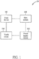
- FIG. 1 is a schematic diagram of a touch display system 10 according to an embodiment of the present application.
- the touch display system 10 includes a panel device 102 and a touch device (not labeled in the figure) connected to the panel device 102.
- the touch device includes a touch circuit 104, a power supply circuit 106 and a host system 108.
- the panel device 102 is utilized for providing a reference signal, for example, the reference signal may be a signal generated when a common voltage (VCOM) layer of a sub-pixel of Indium Tin Oxide (ITO) of the LCD panel is driven by a direct current or an alternate current (e.g. an ACVCOM and DCVCOM LCD panel).
- VCOM common voltage
- ITO Indium Tin Oxide
- the touch circuit 104 is connected to the panel device 102, and the touch circuit 104 takes the reference signal of the panel device 102 as a signal source of a ground terminal of the touch circuit 104.
- the touch circuit 104 is utilized for generating a signal, e.g., a touch signal when receiving a finger touch, so as to determine a location where an electrode was touched; for example, when the panel device 102 is implemented by the LCD panel and receives the finger touch, the touch circuit of the LCD panel, which includes electrodes, generates a capacitive electrode variation signal, and the touch circuit takes the signal from the VCOM layer of ITO of the LCD panel as the signal source of the ground terminal.
- the power supply circuit 106 is connected to the touch circuit 104, for providing power for the touch circuit 104, and converting a level of a communication signal between the touch circuit 104 and the host system 108.
- the host system 108 is connected to the panel device 102 and the power supply circuit 106; for example, the host system 108 may be implemented by a mobile phone or a tablet computer, for receiving a signal level from the touch circuit 104, which is converted by the power supply circuit 106, so as to communicate with the touch circuit 104; for example, the touch circuit determines a location where the finger touches on the LCD panel, transmits a location signal to the host system 108 (i.e. the mobile phone or the tablet computer), and displays an interaction on the panel device.
- the host system 108 i.e. the mobile phone or the tablet computer
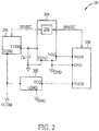
- FIG. 2 is a schematic diagram of a circuit structure of a touch display system 20 according to an embodiment of the present application.
- the circuit structure of the touch display system 20 includes a panel device 202, a touch circuit 204, a power supply circuit 206 and a host system 208.
- the panel device 202 is connected to the touch circuit 204 and the host system 208, for providing a reference signal VCOM for the touch circuit 204.
- the touch circuit 204 is utilized for generating a signal when the panel device 202 receives a finger touch, so as to determine a location where an electrode was touched, and receive the reference signal VCOM from the panel device 202.
- the power supply circuit 206 is connected to the touch circuit 204 for providing power for the touch circuit 204, and includes a level shifter 210 for converting a level of a communication signal between the touch circuit 204 and the host system 208.
- the host system 208 i.e. a mobile phone or a tablet computer
- the host system 208 is connected to the panel device 202 and the touch circuit 204, for providing power source for the panel device 202 and communicating with the touch circuit 204.
- the panel device 202 of the embodiment of the present disclosure provides a reference signal VCOM to a ground terminal TGND of the touch circuit 204, such that the ground of the touch circuit 204 is from the reference signal VOCM, which generates the noises, so as to prevent the touch circuit 204 from suffering the noise interferences, which is from the panel device 202 being scanned and caused by the ITO VCOM layer driven by a high voltage, and to improve the received signal quality of the touch circuit 204.
- the power supply circuit 206 converts, by a level shifter 210, a level of a communication signal between the touch circuit 204 and the host system 208 transmitted via the Serial Peripheral Interface (SPI) or the Inter Integrated Circuit Communications (I2C) bus. That is, the level shifter 210 converts the communication signal between the touch circuit 204 and the host system 208, such that the level between the touch circuit 204 and the host system 208 is consistent when transmitting the communication signal.
- SPI Serial Peripheral Interface
- I2C Inter Integrated Circuit Communications
- a working voltage TVDD of the touch circuit 204 is lower than a working voltage VDD1 of the host system 208; under this circumstance, the power of the touch circuit 204 is provided by the host system 208.
- the reference signal VCOM of the ground terminal TGND of the touch circuit 204 is provided by the power supply circuit 206, and the reference signal VCOM is a floating signal, which results in that the working voltage TVDD of the touch circuit 204 may be higher than the working voltage VDD1 of the host system 208 sometimes. In this situation, the host system 208 may not be able to supply stable power for the touch circuit 204.
- the power supply circuit 206 may stably supply the power for the touch circuit 204 when the working voltage TVDD of the touch circuit 204 is higher than the working voltage VDD1 of the host system 208.
- the panel device provides the reference signal and the power supply circuit provides the power for the touch circuit, such that the touch circuit may avoid the noise interferences generated by the panel device and obtain a clearer signal with higher quality.
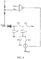
- the power supply circuit 206 of the present application may be implemented by a charge pump, e.g. please refer to FIG. 3 and FIG. 4 , which are the power supply circuit 206 according to embodiments of the present application.
- capacitors C1 and C2 of internal circuit of a capacitive charge pump can be used to store energy, and switches CK1, CK2 are alternatively switched on and switched off to perform a voltage conversion between DC/DC.
- FIG. 4 when the switch CK1 is switched on, the voltage VDD is configured to charge the capacitor C1; when the switch CK1 is switched off and the switch CK2 is switched on, the voltage VDD charges the capacitor C2, such that the capacitive charge pump may be one of the examples for implementing the power supply circuit of the present disclosure.
- FIG. 4 further adds a non-inverting closed loop operational amplifier as one example of implementing the power supply circuit, and not limited thereto, and all kinds of devices capable of implementing the charge pump are suitable for the present application.
- the power supply circuit 206 may provide a high voltage signal for the touch device under a high voltage process, and further improve the SNR of the touch circuit, which belongs to the scope of the present disclosure.
- the embodiments of the present application utilize the reference signal provided by the panel device as the signal source of the ground terminal of the touch circuit, and utilizes the power supply circuit for providing the power to the touch circuit, so as to avoid the effect of the noises caused by the panel device on the touch circuit, and may improve the signal quality of the touch circuit.
Landscapes
- Engineering & Computer Science (AREA)
- Theoretical Computer Science (AREA)
- General Engineering & Computer Science (AREA)
- Physics & Mathematics (AREA)
- General Physics & Mathematics (AREA)
- Human Computer Interaction (AREA)
- Nonlinear Science (AREA)
- Crystallography & Structural Chemistry (AREA)
- Optics & Photonics (AREA)
- Chemical & Material Sciences (AREA)
- Mathematical Physics (AREA)
- Position Input By Displaying (AREA)
- Control Of Indicators Other Than Cathode Ray Tubes (AREA)
Abstract
Description
- The present application relates to a touch device and touch display system, and more particularly, to a touch device capable of eliminating internal noise of a touch circuit of the touch display system and a touch display system adopting the touch device.
- With the advantage and development of technology, mobile phones, digital cameras, tablet computers, laptops and mobile electronic devices have become indispensable tools to human life. In order to achieve a more efficient working way, touch devices have been utilized in all kinds of electronic devices, for example, inductive and capacitive touch devices, touch panels and so on. However, since the conventional touch device is often connected to the liquid-crystal display (LCD) panel driven by a high voltage, when a driving circuit drives the LCD panel, interferences or noises are generated, which affects quality of a received signal scanned by a touch circuit of the touch device.
- Therefore, how to provide a touch display system capable of eliminating the noises from the LCD panel device, and improving the signal quality of the touch display system, has become one of objectives in the industry.
- Therefore, one major objective of the present disclosure is to provide a touch display system capable of eliminating the noises from the panel device and improving the quality of the touch signal.
- To solve the above mentioned technical problems, an embodiment of the present application provides a touch device, including a touch circuit which is connected a panel device and configured to generate a signal according to a touch on the panel device by an external object, and the touch circuit is configured to receive a reference signal provided by the panel device as a signal source of a ground terminal of the touch circuit; a power supply circuit, connected to the touch circuit, is configured to provide power for the touch circuit; and a host system, connected to the touch circuit, is configured to receive the signal generated by the touch circuit.
- Optionally, the reference signal is generated by a common electrode layer of a sub-pixel of the panel device, when the panel device is driven by a direct current or an alternate current.
- Optionally, the touch circuit has a first working voltage, the host system has a second working voltage, when the first working voltage is higher than the second working voltage, and the power supply circuit is configured to provide power for the touch circuit.
- Optionally, when the second working voltage is higher than the first working voltage, the host system is configured to provide power for the touch circuit.
- Optionally, the power supply circuit further includes a level shifter configured to convert a level of a communication signal between the touch circuit and the host system.
- Optionally, the reference signal is a floating signal.
- To better solve the above mentioned technical problems, an embodiment of the present application provides a touch display system includes a panel device and a touch device, wherein the touch device includes a touch circuit, the touch circuit is connected to the panel device and configured to generate a signal according to a touch on the panel device by an external object, and the touch circuit is configured to receive a reference signal provided by the panel device as a signal source of a ground terminal of the touch circuit; a power supply circuit, connected to the touch circuit, is configured to provide power for the touch circuit; and a host system, connected to the touch circuit, is configured to receive the signal generated by the touch circuit.
- The touch display system provided by the present application takes the reference signal of the panel device as the ground signal of the touch circuit, and the power supply circuit provides power for the touch circuit, so as to eliminate the noises from the panel device and improve the signal quality of the touch display system.
- These and other objectives of the present disclosure will no doubt become obvious to those of ordinary skill in the art after reading the following detailed description of the preferred embodiment that is illustrated in the various figures and drawings.
- One or more exemplary embodiments are illustrated by the drawings corresponding to figures, these illustrative embodiments do not constitute limitations to the embodiments, the elements denoted by the same reference numerals in the figures are similar elements, and unless specific statement, the figures do not constitute scale limitations.
-
FIG. 1 is a schematic diagram of a touch display system according to an embodiment of the present application; -
FIG. 2 is a schematic diagram of a circuit structure of a touch display system according to an embodiment of the present application; -
FIG. 3 is a schematic diagram of a power supply circuit according to an embodiment of the present application; -
FIG. 4 is a schematic diagram of another power supply circuit according to an embodiment of the present application. - In order to make the objects, technical solutions and advantages of the present disclosure become more apparent, the following relies on the accompanying drawings and embodiments to describe the present disclosure in further detail. It should be understood that the specific embodiments described herein are only for explaining the present disclosure and are not intended to limit the present disclosure.
- Please refer to
FIG. 1 , which is a schematic diagram of atouch display system 10 according to an embodiment of the present application. Thetouch display system 10 includes apanel device 102 and a touch device (not labeled in the figure) connected to thepanel device 102. The touch device includes atouch circuit 104, apower supply circuit 106 and ahost system 108. Thepanel device 102 is utilized for providing a reference signal, for example, the reference signal may be a signal generated when a common voltage (VCOM) layer of a sub-pixel of Indium Tin Oxide (ITO) of the LCD panel is driven by a direct current or an alternate current (e.g. an ACVCOM and DCVCOM LCD panel). Thetouch circuit 104 is connected to thepanel device 102, and thetouch circuit 104 takes the reference signal of thepanel device 102 as a signal source of a ground terminal of thetouch circuit 104. Thetouch circuit 104 is utilized for generating a signal, e.g., a touch signal when receiving a finger touch, so as to determine a location where an electrode was touched; for example, when thepanel device 102 is implemented by the LCD panel and receives the finger touch, the touch circuit of the LCD panel, which includes electrodes, generates a capacitive electrode variation signal, and the touch circuit takes the signal from the VCOM layer of ITO of the LCD panel as the signal source of the ground terminal. Thepower supply circuit 106 is connected to thetouch circuit 104, for providing power for thetouch circuit 104, and converting a level of a communication signal between thetouch circuit 104 and thehost system 108. In addition, thehost system 108 is connected to thepanel device 102 and thepower supply circuit 106; for example, thehost system 108 may be implemented by a mobile phone or a tablet computer, for receiving a signal level from thetouch circuit 104, which is converted by thepower supply circuit 106, so as to communicate with thetouch circuit 104; for example, the touch circuit determines a location where the finger touches on the LCD panel, transmits a location signal to the host system 108 (i.e. the mobile phone or the tablet computer), and displays an interaction on the panel device. - Please continue to refer to
FIG. 2 , which is a schematic diagram of a circuit structure of atouch display system 20 according to an embodiment of the present application. In this embodiment, the circuit structure of thetouch display system 20 includes apanel device 202, atouch circuit 204, apower supply circuit 206 and ahost system 208. As shown inFIG. 2 , thepanel device 202 is connected to thetouch circuit 204 and thehost system 208, for providing a reference signal VCOM for thetouch circuit 204. Thetouch circuit 204 is utilized for generating a signal when thepanel device 202 receives a finger touch, so as to determine a location where an electrode was touched, and receive the reference signal VCOM from thepanel device 202. Thepower supply circuit 206 is connected to thetouch circuit 204 for providing power for thetouch circuit 204, and includes alevel shifter 210 for converting a level of a communication signal between thetouch circuit 204 and thehost system 208. The host system 208 (i.e. a mobile phone or a tablet computer) is connected to thepanel device 202 and thetouch circuit 204, for providing power source for thepanel device 202 and communicating with thetouch circuit 204. - In detail, since the VCOM layer of the sub-pixel of the LCD panel generates huge noises or interferences and affects the touch signal, when driven by the DC current or the AC current, the
panel device 202 of the embodiment of the present disclosure provides a reference signal VCOM to a ground terminal TGND of thetouch circuit 204, such that the ground of thetouch circuit 204 is from the reference signal VOCM, which generates the noises, so as to prevent thetouch circuit 204 from suffering the noise interferences, which is from thepanel device 202 being scanned and caused by the ITO VCOM layer driven by a high voltage, and to improve the received signal quality of thetouch circuit 204. In addition, in order to accord the level between thetouch circuit 204 and thehost system 208, thepower supply circuit 206 converts, by alevel shifter 210, a level of a communication signal between thetouch circuit 204 and thehost system 208 transmitted via the Serial Peripheral Interface (SPI) or the Inter Integrated Circuit Communications (I2C) bus. That is, thelevel shifter 210 converts the communication signal between thetouch circuit 204 and thehost system 208, such that the level between thetouch circuit 204 and thehost system 208 is consistent when transmitting the communication signal. Notably, in general, a working voltage TVDD of thetouch circuit 204 is lower than a working voltage VDD1 of thehost system 208; under this circumstance, the power of thetouch circuit 204 is provided by thehost system 208. However, since the reference signal VCOM of the ground terminal TGND of thetouch circuit 204 is provided by thepower supply circuit 206, and the reference signal VCOM is a floating signal, which results in that the working voltage TVDD of thetouch circuit 204 may be higher than the working voltage VDD1 of thehost system 208 sometimes. In this situation, thehost system 208 may not be able to supply stable power for thetouch circuit 204. Therefore, in this example, thepower supply circuit 206 may stably supply the power for thetouch circuit 204 when the working voltage TVDD of thetouch circuit 204 is higher than the working voltage VDD1 of thehost system 208. In this way, the panel device provides the reference signal and the power supply circuit provides the power for the touch circuit, such that the touch circuit may avoid the noise interferences generated by the panel device and obtain a clearer signal with higher quality. - Note that, the embodiments stated above are utilized for illustrating the spirit of the present application, those skilled people in the art may make modifications and alternations, and not limited thereto. For example, the
power supply circuit 206 of the present application may be implemented by a charge pump, e.g. please refer toFIG. 3 andFIG. 4 , which are thepower supply circuit 206 according to embodiments of the present application. As shown inFIG. 3 , capacitors C1 and C2 of internal circuit of a capacitive charge pump can be used to store energy, and switches CK1, CK2 are alternatively switched on and switched off to perform a voltage conversion between DC/DC. That is, when the switch CK1 is switched on, the voltage VDD is configured to charge the capacitor C1; when the switch CK1 is switched off and the switch CK2 is switched on, the voltage VDD charges the capacitor C2, such that the capacitive charge pump may be one of the examples for implementing the power supply circuit of the present disclosure. In another embodiment, please refer toFIG. 4 , different fromFIG. 3 ,FIG. 4 further adds a non-inverting closed loop operational amplifier as one example of implementing the power supply circuit, and not limited thereto, and all kinds of devices capable of implementing the charge pump are suitable for the present application. In addition, thepower supply circuit 206 may provide a high voltage signal for the touch device under a high voltage process, and further improve the SNR of the touch circuit, which belongs to the scope of the present disclosure. - In summary, the embodiments of the present application utilize the reference signal provided by the panel device as the signal source of the ground terminal of the touch circuit, and utilizes the power supply circuit for providing the power to the touch circuit, so as to avoid the effect of the noises caused by the panel device on the touch circuit, and may improve the signal quality of the touch circuit.
- Those skilled in the art will readily observe that numerous modifications and alterations of the device and method may be made while retaining the teachings of the disclosure. Accordingly, the above disclosure should be construed as limited only by the metes and bounds of the appended claims.
Claims (12)
- A touch device, comprising:a touch circuit, connected to a panel device and configured to generate a signal according to a touch on the panel device by an external object, wherein the touch circuit is configured to receive a reference signal provided by the panel device as a signal source of a ground terminal of the touch circuit;a power supply circuit, connected to the touch circuit, is configured to provide power for the touch circuit; anda host system, connected to the touch circuit, is configured to receive the signal generated by the touch circuit.
- The touch device of claim 1, wherein the reference signal is generated by a common electrode layer of a sub-pixel of the panel device when the panel device is driven by a direct current or an alternate current.
- The touch device of claim 1, wherein the touch circuit has a first working voltage, the host system has a second working voltage, wherein when the first working voltage is higher than the second working voltage, the power supply circuit is configured to provide power for the touch circuit.
- The touch device of claim 3, wherein when the second working voltage is higher than the first working voltage, the host system is configured to provide power for the touch circuit.
- The touch device of claim 1, wherein the power supply circuit further comprises a level shifter, wherein the level shifter is configured to convert a level of a communication signal between the touch circuit and the host system.
- The touch device of claim 1, wherein the reference signal is a floating signal.
- A touch display system, comprising:a panel device; anda touch device, comprising:a touch circuit, connected to the panel device and is configured to generate a signal according to a touch on the panel device by an external object, wherein the touch circuit is configured to receive a reference signal provided by the panel device as a signal source of a ground terminal of the touch circuit;a power supply circuit, connected to the touch circuit, is configured to provide power for the touch circuit; anda host system, connected to the touch circuit, is configured to receive the signal generated by the touch circuit.
- The touch display system of claim 7, wherein the reference signal is generated by a common electrode layer of a sub-pixel of the panel device when the panel device is driven by a direct current or an alternate current.
- The touch display system of claim 7, wherein the touch circuit has a first working voltage, the host system has a second working voltage, when the first working voltage is higher than the second working voltage, the power supply circuit is configured to provide power for the touch circuit.
- The touch display system of claim 9, wherein when the second working voltage is higher than the first working voltage, the host system is configured to provide power for the touch circuit.
- The touch display system of claim 7, wherein the power supply circuit further includes a level shifter configured to for convert a level of a communication signal between the touch circuit and the host system.
- The touch display system of claim 7, wherein the reference signal is a floating signal.
Applications Claiming Priority (1)
| Application Number | Priority Date | Filing Date | Title |
|---|---|---|---|
| PCT/CN2016/113312 WO2018119961A1 (en) | 2016-12-30 | 2016-12-30 | Touch device and touch display system |
Publications (2)
| Publication Number | Publication Date |
|---|---|
| EP3396501A1 true EP3396501A1 (en) | 2018-10-31 |
| EP3396501A4 EP3396501A4 (en) | 2019-04-24 |
Family
ID=62706980
Family Applications (1)
| Application Number | Title | Priority Date | Filing Date |
|---|---|---|---|
| EP16920448.4A Ceased EP3396501A4 (en) | 2016-12-30 | 2016-12-30 | TOUCH DEVICE AND TOUCH DISPLAY SYSTEM |
Country Status (5)
| Country | Link |
|---|---|
| US (1) | US10642393B2 (en) |
| EP (1) | EP3396501A4 (en) |
| KR (1) | KR102090509B1 (en) |
| CN (1) | CN109478109A (en) |
| WO (1) | WO2018119961A1 (en) |
Families Citing this family (1)
| Publication number | Priority date | Publication date | Assignee | Title |
|---|---|---|---|---|
| US10521045B2 (en) * | 2018-02-14 | 2019-12-31 | Microchip Technology Incorporated | Reference noise rejection improvement based on sample and hold circuitry |
Family Cites Families (13)
| Publication number | Priority date | Publication date | Assignee | Title |
|---|---|---|---|---|
| KR101328387B1 (en) * | 2006-08-25 | 2013-11-13 | 삼성디스플레이 주식회사 | Method of touch position detecting |
| KR101398238B1 (en) * | 2010-10-01 | 2014-05-22 | 엘지디스플레이 주식회사 | Display device having touch screen panel |
| TWI461979B (en) * | 2012-03-19 | 2014-11-21 | Mstar Semiconductor Inc | Control system for touch screen |
| KR102033614B1 (en) * | 2012-12-13 | 2019-10-17 | 엘지디스플레이 주식회사 | Touch sensor integrated type display device |
| CN103135851B (en) * | 2013-02-28 | 2016-05-04 | 合肥京东方光电科技有限公司 | A kind of contact panel and touch display screen |
| US10845901B2 (en) * | 2013-07-31 | 2020-11-24 | Apple Inc. | Touch controller architecture |
| JP2015176512A (en) * | 2014-03-18 | 2015-10-05 | シナプティクス・ディスプレイ・デバイス合同会社 | semiconductor device |
| TW201624213A (en) * | 2014-12-19 | 2016-07-01 | 中華映管股份有限公司 | Touch display device and noise-shielding method of touch display device |
| WO2016195388A1 (en) * | 2015-06-04 | 2016-12-08 | 주식회사 실리콘웍스 | Technology for driving a panel |
| KR102484984B1 (en) * | 2015-06-09 | 2023-01-06 | 주식회사 엘엑스세미콘 | Techniques for driving panel |
| CN105335009B (en) * | 2015-12-03 | 2023-08-08 | 敦泰科技(深圳)有限公司 | Touch display device and electronic equipment |
| CN105335010B (en) * | 2015-12-03 | 2025-01-21 | 敦泰科技(深圳)有限公司 | Touch display device and electronic device |
| CN105353920B (en) * | 2015-12-07 | 2018-09-07 | 上海中航光电子有限公司 | A kind of integrated touch-control display panel and touch control display device |
-
2016
- 2016-12-30 KR KR1020187014701A patent/KR102090509B1/en not_active Expired - Fee Related
- 2016-12-30 CN CN201680002050.0A patent/CN109478109A/en active Pending
- 2016-12-30 WO PCT/CN2016/113312 patent/WO2018119961A1/en not_active Ceased
- 2016-12-30 EP EP16920448.4A patent/EP3396501A4/en not_active Ceased
-
2018
- 2018-05-08 US US15/973,546 patent/US10642393B2/en not_active Expired - Fee Related
Also Published As
| Publication number | Publication date |
|---|---|
| US10642393B2 (en) | 2020-05-05 |
| US20180253177A1 (en) | 2018-09-06 |
| CN109478109A (en) | 2019-03-15 |
| EP3396501A4 (en) | 2019-04-24 |
| KR102090509B1 (en) | 2020-03-19 |
| WO2018119961A1 (en) | 2018-07-05 |
| KR20180090265A (en) | 2018-08-10 |
Similar Documents
| Publication | Publication Date | Title |
|---|---|---|
| CN103324367B (en) | Touch-sensing equipment and double sampling method thereof | |
| US9348476B2 (en) | Display device with integrated touch screen and driving method thereof | |
| US9329739B2 (en) | Touch sensing system and method of controlling power consumption thereof, and display device using the same | |
| CN103902121B (en) | Touch detecting apparatus, the display device with touching detection function and electronic equipment | |
| US9910333B2 (en) | Display device | |
| CN103513814A (en) | Display device with integrated touch screen | |
| US11216120B2 (en) | Touch panel and driving method thereof, and touch device | |
| US10241629B2 (en) | Filtering circuit and touch display device | |
| CN104375733A (en) | Touch display screen driving circuit and method | |
| CN102270070A (en) | Light sensing device suitable for optical touch display panel | |
| CN105070268B (en) | Reduce the method and apparatus of the leakage current of embedded touch LCD panel | |
| CN211554959U (en) | Electronic device with fingerprint sensing function | |
| CN104199577A (en) | Method and circuit of providing synchronous signals for touch panel by display panel | |
| CN107346189B (en) | touch monitor | |
| CN108415633B (en) | Touch display screen and touch display device | |
| US10642393B2 (en) | Touch device and touch display system for eliminating noise in panel device | |
| CN106201151B (en) | Display panel and electronic equipment | |
| US20190079632A1 (en) | Electrical device, receiving circuit, and method for touch sensing | |
| CN109271054B (en) | Touch Display Driver Circuit | |
| CN108780371B (en) | Touch system and its power supply circuit | |
| CN102193226A (en) | Panel with Proximity Sensing | |
| CN210405086U (en) | Voltage conversion devices, chips, display panels and electronic equipment | |
| CN112087130B (en) | Voltage conversion device, chip and electronic device | |
| CN202939582U (en) | Touch controlling display screen | |
| CN101154359A (en) | Image display system and method of driving an AC signal generating circuit |
Legal Events
| Date | Code | Title | Description |
|---|---|---|---|
| STAA | Information on the status of an ep patent application or granted ep patent |
Free format text: STATUS: UNKNOWN |
|
| STAA | Information on the status of an ep patent application or granted ep patent |
Free format text: STATUS: THE INTERNATIONAL PUBLICATION HAS BEEN MADE |
|
| PUAI | Public reference made under article 153(3) epc to a published international application that has entered the european phase |
Free format text: ORIGINAL CODE: 0009012 |
|
| STAA | Information on the status of an ep patent application or granted ep patent |
Free format text: STATUS: REQUEST FOR EXAMINATION WAS MADE |
|
| 17P | Request for examination filed |
Effective date: 20180508 |
|
| AK | Designated contracting states |
Kind code of ref document: A1 Designated state(s): AL AT BE BG CH CY CZ DE DK EE ES FI FR GB GR HR HU IE IS IT LI LT LU LV MC MK MT NL NO PL PT RO RS SE SI SK SM TR |
|
| AX | Request for extension of the european patent |
Extension state: BA ME |
|
| RIN1 | Information on inventor provided before grant (corrected) |
Inventor name: YANG, MENG-TA |
|
| R17P | Request for examination filed (corrected) |
Effective date: 20180508 |
|
| A4 | Supplementary search report drawn up and despatched |
Effective date: 20190321 |
|
| RIC1 | Information provided on ipc code assigned before grant |
Ipc: G06F 3/041 20060101AFI20190315BHEP Ipc: G06F 3/044 20060101ALI20190315BHEP |
|
| DAV | Request for validation of the european patent (deleted) | ||
| DAX | Request for extension of the european patent (deleted) | ||
| STAA | Information on the status of an ep patent application or granted ep patent |
Free format text: STATUS: EXAMINATION IS IN PROGRESS |
|
| 17Q | First examination report despatched |
Effective date: 20200518 |
|
| REG | Reference to a national code |
Ref country code: DE Ref legal event code: R003 |
|
| STAA | Information on the status of an ep patent application or granted ep patent |
Free format text: STATUS: THE APPLICATION HAS BEEN REFUSED |
|
| 18R | Application refused |
Effective date: 20211023 |