EP3394581B1 - Temperature sensor - Google Patents
Temperature sensor Download PDFInfo
- Publication number
- EP3394581B1 EP3394581B1 EP16822172.9A EP16822172A EP3394581B1 EP 3394581 B1 EP3394581 B1 EP 3394581B1 EP 16822172 A EP16822172 A EP 16822172A EP 3394581 B1 EP3394581 B1 EP 3394581B1
- Authority
- EP
- European Patent Office
- Prior art keywords
- temperature
- temperature sensor
- light emitter
- current
- sensor according
- Prior art date
- Legal status (The legal status is an assumption and is not a legal conclusion. Google has not performed a legal analysis and makes no representation as to the accuracy of the status listed.)
- Active
Links
- 230000002441 reversible effect Effects 0.000 claims description 54
- 230000003287 optical effect Effects 0.000 claims description 24
- 229910002601 GaN Inorganic materials 0.000 claims description 9
- 230000000694 effects Effects 0.000 claims description 9
- 239000000463 material Substances 0.000 claims description 9
- 238000005259 measurement Methods 0.000 claims description 6
- OYPRJOBELJOOCE-UHFFFAOYSA-N Calcium Chemical compound [Ca] OYPRJOBELJOOCE-UHFFFAOYSA-N 0.000 claims description 5
- JMASRVWKEDWRBT-UHFFFAOYSA-N Gallium nitride Chemical compound [Ga]#N JMASRVWKEDWRBT-UHFFFAOYSA-N 0.000 claims description 5
- 239000000126 substance Substances 0.000 claims description 5
- 229910052791 calcium Inorganic materials 0.000 claims description 4
- 239000011575 calcium Substances 0.000 claims description 4
- 230000001413 cellular effect Effects 0.000 claims description 4
- 239000004065 semiconductor Substances 0.000 claims description 4
- 238000012546 transfer Methods 0.000 claims description 4
- 239000005952 Aluminium phosphide Substances 0.000 claims description 3
- 229910005540 GaP Inorganic materials 0.000 claims description 3
- 239000005083 Zinc sulfide Substances 0.000 claims description 3
- PPNXXZIBFHTHDM-UHFFFAOYSA-N aluminium phosphide Chemical compound P#[Al] PPNXXZIBFHTHDM-UHFFFAOYSA-N 0.000 claims description 3
- NWAIGJYBQQYSPW-UHFFFAOYSA-N azanylidyneindigane Chemical compound [In]#N NWAIGJYBQQYSPW-UHFFFAOYSA-N 0.000 claims description 3
- PMHQVHHXPFUNSP-UHFFFAOYSA-M copper(1+);methylsulfanylmethane;bromide Chemical compound Br[Cu].CSC PMHQVHHXPFUNSP-UHFFFAOYSA-M 0.000 claims description 3
- HZXMRANICFIONG-UHFFFAOYSA-N gallium phosphide Chemical compound [Ga]#P HZXMRANICFIONG-UHFFFAOYSA-N 0.000 claims description 3
- AZUPEYZKABXNLR-UHFFFAOYSA-N magnesium;selenium(2-) Chemical compound [Mg+2].[Se-2] AZUPEYZKABXNLR-UHFFFAOYSA-N 0.000 claims description 3
- 150000003346 selenoethers Chemical class 0.000 claims description 3
- HBMJWWWQQXIZIP-UHFFFAOYSA-N silicon carbide Chemical compound [Si+]#[C-] HBMJWWWQQXIZIP-UHFFFAOYSA-N 0.000 claims description 3
- 229910010271 silicon carbide Inorganic materials 0.000 claims description 3
- SMDQFHZIWNYSMR-UHFFFAOYSA-N sulfanylidenemagnesium Chemical compound S=[Mg] SMDQFHZIWNYSMR-UHFFFAOYSA-N 0.000 claims description 3
- 239000011701 zinc Substances 0.000 claims description 3
- DRDVZXDWVBGGMH-UHFFFAOYSA-N zinc;sulfide Chemical compound [S-2].[Zn+2] DRDVZXDWVBGGMH-UHFFFAOYSA-N 0.000 claims description 3
- 210000001519 tissue Anatomy 0.000 description 21
- 238000000034 method Methods 0.000 description 14
- 210000004027 cell Anatomy 0.000 description 10
- 238000013461 design Methods 0.000 description 10
- 239000007943 implant Substances 0.000 description 9
- 230000000638 stimulation Effects 0.000 description 9
- 238000004088 simulation Methods 0.000 description 8
- 238000010586 diagram Methods 0.000 description 6
- 230000006870 function Effects 0.000 description 6
- 230000000149 penetrating effect Effects 0.000 description 6
- 238000013459 approach Methods 0.000 description 5
- 230000007774 longterm Effects 0.000 description 5
- 102000004169 proteins and genes Human genes 0.000 description 5
- 108090000623 proteins and genes Proteins 0.000 description 5
- 238000012360 testing method Methods 0.000 description 5
- 230000015572 biosynthetic process Effects 0.000 description 4
- 230000001419 dependent effect Effects 0.000 description 4
- 238000005755 formation reaction Methods 0.000 description 4
- 230000001537 neural effect Effects 0.000 description 4
- 230000008859 change Effects 0.000 description 3
- 239000011162 core material Substances 0.000 description 3
- 238000002001 electrophysiology Methods 0.000 description 3
- 238000002474 experimental method Methods 0.000 description 3
- 238000004458 analytical method Methods 0.000 description 2
- 230000036760 body temperature Effects 0.000 description 2
- 238000005516 engineering process Methods 0.000 description 2
- 238000010438 heat treatment Methods 0.000 description 2
- 238000003384 imaging method Methods 0.000 description 2
- 230000028709 inflammatory response Effects 0.000 description 2
- 238000012544 monitoring process Methods 0.000 description 2
- 238000002161 passivation Methods 0.000 description 2
- 230000008569 process Effects 0.000 description 2
- 230000006798 recombination Effects 0.000 description 2
- 238000005215 recombination Methods 0.000 description 2
- 230000004044 response Effects 0.000 description 2
- ULWRKVIIQSVFIZ-YMNIQAILSA-N (2s)-2-amino-5-[carboxy-(2-nitrophenyl)methoxy]-5-oxopentanoic acid Chemical compound OC(=O)[C@@H](N)CCC(=O)OC(C(O)=O)C1=CC=CC=C1[N+]([O-])=O ULWRKVIIQSVFIZ-YMNIQAILSA-N 0.000 description 1
- 229910000980 Aluminium gallium arsenide Inorganic materials 0.000 description 1
- 108091005462 Cation channels Proteins 0.000 description 1
- 102000003688 G-Protein-Coupled Receptors Human genes 0.000 description 1
- 108090000045 G-Protein-Coupled Receptors Proteins 0.000 description 1
- 229910001218 Gallium arsenide Inorganic materials 0.000 description 1
- 108010043121 Green Fluorescent Proteins Proteins 0.000 description 1
- 102000004144 Green Fluorescent Proteins Human genes 0.000 description 1
- 102000006391 Ion Pumps Human genes 0.000 description 1
- 108010083687 Ion Pumps Proteins 0.000 description 1
- 208000018737 Parkinson disease Diseases 0.000 description 1
- 206010037660 Pyrexia Diseases 0.000 description 1
- 206010044565 Tremor Diseases 0.000 description 1
- 239000000370 acceptor Substances 0.000 description 1
- 230000001154 acute effect Effects 0.000 description 1
- 230000003044 adaptive effect Effects 0.000 description 1
- 210000001130 astrocyte Anatomy 0.000 description 1
- 230000004888 barrier function Effects 0.000 description 1
- 230000000975 bioactive effect Effects 0.000 description 1
- 239000007844 bleaching agent Substances 0.000 description 1
- 210000004556 brain Anatomy 0.000 description 1
- 239000003990 capacitor Substances 0.000 description 1
- 230000003915 cell function Effects 0.000 description 1
- 230000033077 cellular process Effects 0.000 description 1
- 238000005229 chemical vapour deposition Methods 0.000 description 1
- 230000001684 chronic effect Effects 0.000 description 1
- 238000005253 cladding Methods 0.000 description 1
- 230000000295 complement effect Effects 0.000 description 1
- 230000003247 decreasing effect Effects 0.000 description 1
- 238000011161 development Methods 0.000 description 1
- 206010012601 diabetes mellitus Diseases 0.000 description 1
- 238000003745 diagnosis Methods 0.000 description 1
- 238000009792 diffusion process Methods 0.000 description 1
- 201000010099 disease Diseases 0.000 description 1
- 208000037265 diseases, disorders, signs and symptoms Diseases 0.000 description 1
- 230000007613 environmental effect Effects 0.000 description 1
- 230000001747 exhibiting effect Effects 0.000 description 1
- 239000000835 fiber Substances 0.000 description 1
- 238000001914 filtration Methods 0.000 description 1
- 239000005090 green fluorescent protein Substances 0.000 description 1
- 230000036541 health Effects 0.000 description 1
- 238000001727 in vivo Methods 0.000 description 1
- 239000003999 initiator Substances 0.000 description 1
- 230000003914 insulin secretion Effects 0.000 description 1
- 230000010354 integration Effects 0.000 description 1
- 238000011835 investigation Methods 0.000 description 1
- 230000002427 irreversible effect Effects 0.000 description 1
- 239000003446 ligand Substances 0.000 description 1
- 238000004519 manufacturing process Methods 0.000 description 1
- 230000001404 mediated effect Effects 0.000 description 1
- 229910044991 metal oxide Inorganic materials 0.000 description 1
- 150000004706 metal oxides Chemical class 0.000 description 1
- 238000001451 molecular beam epitaxy Methods 0.000 description 1
- 230000035772 mutation Effects 0.000 description 1
- 210000004165 myocardium Anatomy 0.000 description 1
- 210000005036 nerve Anatomy 0.000 description 1
- 210000003061 neural cell Anatomy 0.000 description 1
- 230000007971 neurological deficit Effects 0.000 description 1
- 210000002569 neuron Anatomy 0.000 description 1
- 210000000056 organ Anatomy 0.000 description 1
- 239000005022 packaging material Substances 0.000 description 1
- 210000000496 pancreas Anatomy 0.000 description 1
- 230000035515 penetration Effects 0.000 description 1
- 238000012805 post-processing Methods 0.000 description 1
- 238000011084 recovery Methods 0.000 description 1
- 238000012552 review Methods 0.000 description 1
- 231100000241 scar Toxicity 0.000 description 1
- 238000004092 self-diagnosis Methods 0.000 description 1
- 230000035945 sensitivity Effects 0.000 description 1
- 230000011664 signaling Effects 0.000 description 1
- 150000003384 small molecules Chemical class 0.000 description 1
- 238000001228 spectrum Methods 0.000 description 1
- 238000007447 staining method Methods 0.000 description 1
- 230000004936 stimulating effect Effects 0.000 description 1
- 230000009772 tissue formation Effects 0.000 description 1
- 230000005740 tumor formation Effects 0.000 description 1
- 238000012795 verification Methods 0.000 description 1
Images







Classifications
-
- G—PHYSICS
- G01—MEASURING; TESTING
- G01K—MEASURING TEMPERATURE; MEASURING QUANTITY OF HEAT; THERMALLY-SENSITIVE ELEMENTS NOT OTHERWISE PROVIDED FOR
- G01K7/00—Measuring temperature based on the use of electric or magnetic elements directly sensitive to heat ; Power supply therefor, e.g. using thermoelectric elements
- G01K7/01—Measuring temperature based on the use of electric or magnetic elements directly sensitive to heat ; Power supply therefor, e.g. using thermoelectric elements using semiconducting elements having PN junctions
-
- A—HUMAN NECESSITIES
- A61—MEDICAL OR VETERINARY SCIENCE; HYGIENE
- A61B—DIAGNOSIS; SURGERY; IDENTIFICATION
- A61B5/00—Measuring for diagnostic purposes; Identification of persons
- A61B5/01—Measuring temperature of body parts ; Diagnostic temperature sensing, e.g. for malignant or inflamed tissue
-
- A—HUMAN NECESSITIES
- A61—MEDICAL OR VETERINARY SCIENCE; HYGIENE
- A61B—DIAGNOSIS; SURGERY; IDENTIFICATION
- A61B5/00—Measuring for diagnostic purposes; Identification of persons
- A61B5/40—Detecting, measuring or recording for evaluating the nervous system
- A61B5/4029—Detecting, measuring or recording for evaluating the nervous system for evaluating the peripheral nervous systems
- A61B5/4041—Evaluating nerves condition
-
- A—HUMAN NECESSITIES
- A61—MEDICAL OR VETERINARY SCIENCE; HYGIENE
- A61B—DIAGNOSIS; SURGERY; IDENTIFICATION
- A61B5/00—Measuring for diagnostic purposes; Identification of persons
- A61B5/48—Other medical applications
- A61B5/4848—Monitoring or testing the effects of treatment, e.g. of medication
-
- A—HUMAN NECESSITIES
- A61—MEDICAL OR VETERINARY SCIENCE; HYGIENE
- A61N—ELECTROTHERAPY; MAGNETOTHERAPY; RADIATION THERAPY; ULTRASOUND THERAPY
- A61N5/00—Radiation therapy
- A61N5/06—Radiation therapy using light
- A61N5/0601—Apparatus for use inside the body
-
- A—HUMAN NECESSITIES
- A61—MEDICAL OR VETERINARY SCIENCE; HYGIENE
- A61N—ELECTROTHERAPY; MAGNETOTHERAPY; RADIATION THERAPY; ULTRASOUND THERAPY
- A61N5/00—Radiation therapy
- A61N5/06—Radiation therapy using light
- A61N5/0613—Apparatus adapted for a specific treatment
- A61N5/0622—Optical stimulation for exciting neural tissue
-
- G—PHYSICS
- G01—MEASURING; TESTING
- G01K—MEASURING TEMPERATURE; MEASURING QUANTITY OF HEAT; THERMALLY-SENSITIVE ELEMENTS NOT OTHERWISE PROVIDED FOR
- G01K7/00—Measuring temperature based on the use of electric or magnetic elements directly sensitive to heat ; Power supply therefor, e.g. using thermoelectric elements
- G01K7/42—Circuits effecting compensation of thermal inertia; Circuits for predicting the stationary value of a temperature
- G01K7/427—Temperature calculation based on spatial modeling, e.g. spatial inter- or extrapolation
-
- A—HUMAN NECESSITIES
- A61—MEDICAL OR VETERINARY SCIENCE; HYGIENE
- A61B—DIAGNOSIS; SURGERY; IDENTIFICATION
- A61B2562/00—Details of sensors; Constructional details of sensor housings or probes; Accessories for sensors
- A61B2562/02—Details of sensors specially adapted for in-vivo measurements
- A61B2562/0271—Thermal or temperature sensors
-
- A—HUMAN NECESSITIES
- A61—MEDICAL OR VETERINARY SCIENCE; HYGIENE
- A61N—ELECTROTHERAPY; MAGNETOTHERAPY; RADIATION THERAPY; ULTRASOUND THERAPY
- A61N5/00—Radiation therapy
- A61N5/06—Radiation therapy using light
- A61N5/0601—Apparatus for use inside the body
- A61N2005/0612—Apparatus for use inside the body using probes penetrating tissue; interstitial probes
-
- A—HUMAN NECESSITIES
- A61—MEDICAL OR VETERINARY SCIENCE; HYGIENE
- A61N—ELECTROTHERAPY; MAGNETOTHERAPY; RADIATION THERAPY; ULTRASOUND THERAPY
- A61N5/00—Radiation therapy
- A61N5/06—Radiation therapy using light
- A61N2005/0626—Monitoring, verifying, controlling systems and methods
- A61N2005/0627—Dose monitoring systems and methods
-
- A—HUMAN NECESSITIES
- A61—MEDICAL OR VETERINARY SCIENCE; HYGIENE
- A61N—ELECTROTHERAPY; MAGNETOTHERAPY; RADIATION THERAPY; ULTRASOUND THERAPY
- A61N5/00—Radiation therapy
- A61N5/06—Radiation therapy using light
- A61N2005/065—Light sources therefor
- A61N2005/0651—Diodes
- A61N2005/0652—Arrays of diodes
-
- A—HUMAN NECESSITIES
- A61—MEDICAL OR VETERINARY SCIENCE; HYGIENE
- A61N—ELECTROTHERAPY; MAGNETOTHERAPY; RADIATION THERAPY; ULTRASOUND THERAPY
- A61N5/00—Radiation therapy
- A61N5/06—Radiation therapy using light
- A61N5/067—Radiation therapy using light using laser light
-
- G—PHYSICS
- G01—MEASURING; TESTING
- G01K—MEASURING TEMPERATURE; MEASURING QUANTITY OF HEAT; THERMALLY-SENSITIVE ELEMENTS NOT OTHERWISE PROVIDED FOR
- G01K2211/00—Thermometers based on nanotechnology
-
- G—PHYSICS
- G01—MEASURING; TESTING
- G01K—MEASURING TEMPERATURE; MEASURING QUANTITY OF HEAT; THERMALLY-SENSITIVE ELEMENTS NOT OTHERWISE PROVIDED FOR
- G01K2217/00—Temperature measurement using electric or magnetic components already present in the system to be measured
Definitions
- the present invention relates to temperature sensors and methods of sensing temperature.
- the invention relates in particular, but not exclusively, to temperature sensors integrated with implantable devices.
- Implantable devices are becoming increasingly important in clinical practice.
- a key target area is in treating neurological deficit.
- pacemakers have been utilized since the 1950's to support proper function of cardiac muscle and have more recently been applied to the brain to treat tremor in conditions such as Parkinson's disease.
- neuroprosthetics there is also a need to monitor and stimulate other organs such as the Pancreas in the case of diabetes.
- Chemical reporters also exist, but these are less desirable as they would need to be continuously infused either because the optically active proteins bleach, or because ligand molecule which attaches them to the target cell breaks. In contrast genetically encoded reporters are continuously produced/recycled by their host cells.
- optical stimulus is possible through optogentic and optochemical methods.
- Traditional optochemical methods have utilized cage structures around a bio-active initiator molecules e.g. caged glutamate. In such structures, ltraviolet light is used to uncage the active part of the molecule and thus biomchemically activate the target cell (e.g. Shoham et al. [3]). This is problematic in-vivo so more recent methodologies have utilized lock and key approaches with photoconformable molecules. E.g. Broichhagen et al. utilize such approaches to insulin secretion [4]. However, perhaps the most useful method is optogenetics. In this case, cells are genetically modified to continuously produce optically sensitive proteins.
- Such optogenetic stimulation can use either channelrhodospsins - light sensitive cation channels [5], halorodopsins - light sensitive ion pumps [6], or melanopsins - light sensitive G-protein coupled receptor systems [7].
- Each has their own relative advantages and a good review of the field has be written by J. Barrett et al. [8]. What is common to all of these approaches is that they require high intensity irradiation of the optical targets.
- the fundamental optically active cores in all of these proteins are derived from conjugated small molecules which are optically active in the ultraviolet (350nm to orange/red 600nm) region of the electromagnetic spectrum. In particular, blue wavelengths in this range are heavily scattered by neural tissue. This means there is a requirement for light delivery in close proximity to these targets. This can be achieved by one of two methods:
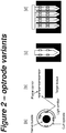
- FIG. 2 There are a number of configurations for illuminating target tissue from photonic implants, as shown in Figure 2 .
- the use depends on the target application.
- cuff style optrodes which can wrap around the bundle are more appropriate ( Figure 2a ).
- Figure 2b For direct stimulation of tissue from the surface, a planar structure is more appropriate ( Figure 2b ).
- penetrating optrodes either in single ( Figure 2c ) or in array formation are most appropriate ( Figure 2d ).
- On-chip temperature sensors have been used to monitor human health for diseases diagnosis and treatment.
- the adaptive multi-sensor CMOS system proposed by Huang et al. [10] comprises different on-chip sensors including temperature sensor.
- This device is capable of body temperature sensing from 32OC to 42OC and also environmental temperature sensing outside the body from -20OC to 120OC.
- Lee et al. presented a low-cost CMOS thermal sensor chip for biomedical application to monitor temperature from 33O C to 42OC with less than 0.15 OC inaccuracy [11].
- bipolar transistors are used to sense temperature and generate the needed reference voltage for sigma-delta analog to digital converter.
- Crepaldi et al proposed a low power CMOS based front-end thermal sensing element with 0.24 OC inaccuracy suitable for biomedical application [12].
- diodes can measure temperatures on a microprocessor belonging to a computer (e.g. die temperature or DieTemp), and methods can sense temperatures on a microprocessor by measuring the current through existing Electrostatic discharge (ESD) devices. It is known in the art from US 2015/117494 A1 , that such diodes can have a more refined sensitivity or accuracy by implementing a "digital circuit" (or control logic) that compares a charge voltage of a capacitor to pre-set upper and lower thresholds. It is also known in the art from Dehkhoda et al. ("Smart Optrode for Neural Stimulation and Sensing", Imperial College London, 2015 ) that electronic circuits may be incorporated directed onto implantable devices in order to determine a diagnostic state.
- ESD Electrostatic discharge
- the present invention proposes to use a light emitter (e.g. a microphotonic component such as a micro LED or laser diode) itself as its own thermal sensor.
- a light emitter e.g. a microphotonic component such as a micro LED or laser diode
- the continued functionality of the device is intrinsically linked to its self-diagnosis.
- microphotonics could be used in implantable devices; opto-electrophysiology, and fluorescence sensing.
- opto-electrophysiology optical methods such as optogenetics are used to provide optical stimulus and/or optical recording of cellular electrical activity.
- Fluorescence sensing the biochemical environment is optically probed with either fluorescence reporter proteins or via cellular autofluorescent signatures. In such scenarios light needs to be delivered to the nervous tissue.
- optically sensitive proteins used in such applications typically tend to be sensitive in the photonic region of UV (350mm) to red (600nm). In this region scattering processes dominate optical traversal of tissue and thus light delivery systems need to be utilized.
- One key form of such a system is to generate light directly, but this can cause localized heating effects at the device surface which may need to be monitored.
- This invention allows such monitoring utilizing the heat producing device itself as a sensor, combined with specific electronic control and signal post-processing.
- the invention provides a temperature sensor for medical use comprising:
- the means for calculating a temperature from the measured reverse current may include a predefined correlation of reverse current versus temperature for the light emitter.
- the temperature that is calculated may be a junction temperature of the light emitter or a surface temperature of the light emitter, for example.
- the temperature may be calculated, for example, using a model that relates surface temperature to the junction temperature of the light emitter (where that is calculated first) or directly to the measured reverse current.
- the model parameters will typically be determined by the implant mass and thermal properties relative to the passivation material.
- the surface temperature may be calculated using a transfer function to determine the surface temperature based on a current/voltage measurement from the light emitter.
- the electrical circuit is configured to maintain the bias voltage at a constant value between 0 and 5V in reverse bias across the optical device.
- the light emitter is, for example a light emitting diode or a stimulated emission device such as a semiconductor laser diode (e.g. in the form of a vertical cavity surface emitting laser). It may be formed, for example in Gallium Nitride, Silicon Carbide, Aluminum Nitride, Indium Nitride, Gallium Phosphide, Aluminium Phosphide, Zinc Sulphide, Magnesium sulphide, Magnesium selenide, or Zn Selenide.
- a light emitting diode or a stimulated emission device such as a semiconductor laser diode (e.g. in the form of a vertical cavity surface emitting laser). It may be formed, for example in Gallium Nitride, Silicon Carbide, Aluminum Nitride, Indium Nitride, Gallium Phosphide, Aluminium Phosphide, Zinc Sulphide, Magnesium sulphide, Magnesium selenide, or Zn Selenide.
- the electrical circuit comprises one or more low pass filters to filter switching noise, whereby the photonic device temperature can be accurately determined despite variations in power supply noise.
- the light emitter has two modes of operation, a temperature sensing mode when a reverse bias voltage is applied across the light emitter and a light emission mode when a forward bias voltage is applied across the light emitter.
- the temperature sensor may be controlled to switch back and forth between the temperature sensing mode and the light emitting mode at a predefined frequency, for example from 1GHz to 10Hz.
- High frequencies e.g. 1MHz - 1GHz
- short pulses e.g. Ins - 1 ⁇ s
- Low frequencies e.g. 10hz - 1MHz
- longer pulses e.g. 100ms - 1 ⁇ s
- optical (primarily neural) tissue stimulation primarily neural
- the temperature sensor can additionally be switched to an off mode in which no voltage is applied across the light emitter.
- the temperature sensor includes a controller for switching the temperature sensor between modes.
- the controller may, for example be configured (e.g. programmed) to switch the temperature sensor between modes at defined time points, pulse widths and/or repetition frequencies.
- the controller may additionally or alternatively be configured to stop subsequent operation in the light emission mode if the calculated temperature exceeds a predefined threshold.
- the predefined threshold may, for example, be in the range 0.1 to 3C above the ambient temperature of the tissue.
- the forward bias voltage is in the range 1.5V - 10V.
- the selected forward bias will depend on the light requirement and optical wavelength. Shorter wavelengths generally need higher bias, as do higher intensities.
- the current in the forward bias is between 1uA to 50mA, dependent on the microphotonic size and required radiant density.
- the invention provides an implantable biomedical device incorporating a temperature sensor as outlined above.
- the device is for optogenetic stimulus of nervous function, wherein the light emitter of the temperature sensor performs optogenetic stimulus when the light emitter is in the light emission mode. In the light emission mode the light emitter of the temperature sensor may perform optogenetic stimulus of electrical activity or chemical activity indirectly via opto-electrical stimulus in non-nervous cells and/or tissue.
- the device may be operable to record cellular electrical or calcium potential in nervous and/or non-nervous tissue.
- the invention proposes use of the temperature sensor to measure temperature by applying the reverse bias across the microphotonic light emitter, measuring the reverse current and calculating the temperature from the measured reverse current.
- microphotonic emitters There are two primary forms of microphotonic emitters that could be used for useful optical interrogation of biological tissue:
- the optically active core material of these emitters could comprise of Gallium Nitride, Silicon Carbide, Aluminum Nitride, Indium Nitride, Gallium Phosphide, Aluminium Phosphide, Zinc Sulphide, Magnesium sulphide, Magnesium Selenide, or Zn Selenide depending on the desired optical properties.
- Gallium Nitride diodes for optical interrogation of astrocyte tissue can be seen in Berlinguer et al [13].
- FIG. 3 shows the results achieved from a standard Gallium Nitride micro-LED incorporating a multiple quantum well architecture. The reverse current of such LEDs change linearly with temperature for a fixed bias voltage ( Figure 3a ), but exponentially with reverse bias ( Figure 3b ).
- an LED per definition is a light emitting diode.
- the diode structure consists of p and n doped layers which are combined in a p-n junction structure.
- the Shockley equation for a p-n junction given by (1) is used to derive the temperature dependency of the reverse current.
- I is the junction current
- Is is the saturation current
- e is the elementary charge
- V is the junction voltage
- n is the ideality factor which is about 1-2
- k is the Boltzmann constant
- T is the absolute temperature in kelvins [10-12].
- the LED saturation Is current can be expressed by
- A is the cross-sectional area of the p-n junction; D n and D p are diffusion constants for electrons and holes exhibiting a T -1/2 temperature dependency; ⁇ n and ⁇ p are the minority carrier lifetimes for electrons and holes supposed to be temperature independent; N D and N A are doping concentration of donors and acceptors which are independent of temperature; Nc and Nv are effective densities of states at the conduction-band and valence-band with temperature dependency of T 3/2 .
- LEDs In practice the theoretical framework of LEDs is more complex. Fundamentally, LEDs generate light by electron-hole recombination. Thus, the efficiency of light generation is a result of the percent of injected current (electrons and holes) which recombine to give our light compared to those that continue to the opposite terminal or recombine non-radiatevely. As a result, LED designers create a multiple quantum well structure with multiple layers of materials of different bandgaps to create trapping centres for recombination.
- a quantum well is a heterostructure with one thin well layer surrounded by two barrier layers. Both electrons and holes are confined in the well layer which is so thin about 40 atomic layers.
- the quantum wells can be grown using molecular beam epitaxy (MBE) [17], and metal-organic chemical vapor deposition (MOCVD) [18].
- MBE molecular beam epitaxy
- MOCVD metal-organic chemical vapor deposition
- the typical materials to be grown can be any sequence of GaAs, AlAs, and AlGaAs.
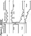
- the multiple quantum well layers act as trapping centres for charge mobility. Escape from such traps is therefore mediated primarily by thermionic emission and quantum tunnelling ( Figure 4 ) over the traps. Both effects are temperature dependent [15, 19] resulting in a linear dependency within the temperature range interesting to this invention.
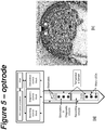
- Figure 5 shows a single penetrating optrode with inbuilt stimulation and recording circuits along its shaft.
- the LED based temperature sensor circuitry is placed close to the ⁇ LEDs to be easily operating in antiphase with optical emission.
- An LED test setup is implemented using GaN LED to extract the needed IR-T curve at different bias voltages.
- the LED under test is placed in an isolated dark box to guarantee that the measured current is only due to the temperature change.
- the box is also temperature isolated to ensure about the accuracy of the measured temperature.
- a hot plate is placed under the LED to increase the temperature which can be measured and recorded by the IR Optris PI camera and the camera interface software, respectively.
- the results achieved from the LED testing experiment are shown in Figure 3 .
- the reverse current of LED is changing linearly with temperature for a fixed bias voltage.
- the reverse current changes with voltage in a fixed temperature.
- a variant or temperature dependent bias voltage can cause a large reverse current variation which is not purely related to temperature variation.
- the designed temperature sensor should provide a fixed temperature independent bias voltage for the LED to avoid current variation because of bias voltage variation.
- FIG. 6 depicts the block diagram of the proposed temperature sensing system based on LED.
- the designed sensing system measures the reverse current of the LED which is reversely biased using a bias voltage. Temperature variation linearly changes this reverse current if a fixed bias voltage is applied across the LED.
- the bias voltage must be precise and temperature independent not to contribute in reverse current changing because the reverse current can change with bias voltage significantly. Therefore, a circuit is needed to provide the bias voltage across the LED and receive its current in same time.
- a second generation current conveyor (CCII) is used at the first stage of the sensor which is capable of providing a precise bias voltage at the input (X) while receiving current using the same input terminal.
- CCII conveys the received current from LED to the output (Z).
- the CCII receives an external bias voltage in other input (Y) and copies this voltage on the input (X) which is supposed to be connected to LED and receive the reverse current.
- VX is match to VY and the output current should follow the current at the input (X).
- a unity current gain for a range of frequencies is needed for the CCII to accurately translate the current changes to temperature variation in the next stages.
- linearity is important for a specific input range of reverse current. Therefore, a robust bias voltage, unity current gain, linearity and low power are the most important specifications in designing the CCII.
- a resistor is used to convert the CCII out current to voltage to be amplified using the amplifier in the last stage.
- the designed amplifier is a single input single output high gain amplifier. This amplifier receives the current variation as voltage in the input and amplifies that to a large signal suitable to digitize using ADC.
- the most important parameters in the design of this amplifier are high gain, low power, high dynamic range, high CMRR and PSRR.
- the common mode rejection properties are determined by matching of transistors and in particular, matching at the input differential stage. This is achieved through enlarging transistors and performing Monte Carlo modelling at the design stage to ensure a probabilistic match.
- the use of larger transistors supports the low pass filtering to reject high frequency power supply noise.
- a negative feedback loop is utilised to support high gain and thermal noise rejection.
- CMOS Complementary Metal Oxide Semiconductor
- the technology node was 0.35 ⁇ m and standard CAD/EDA tools were utilised for its design.
- the schematic of the design is shown in Figure 7 .
- the CCII at first stage receives the LED current in terminal X which has the same vdd voltage as input Y. The received current is copied to the output Z connected to a resistive load [20].
- the second stage includes a two-stage high gain amplifier.
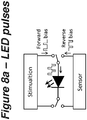
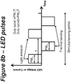
- the sensor circuitry is placed close to the LED which is easily operating in antiphase with optical emission done using stimulation circuits. Temperature sensing is supposed to be performed after LED light emission. In other word, forward biased LED emits light where its intensity can be controlled using pulse width modulation. Then, switching the LED in to the sensor path provides reverse bias for the LED using a specific voltage reference ( Figure 8 ).
- Table 1 lists different examples for LED timing operation.
- PW1 is used to stimulate the LED by providing the forward bias. After this operation, temperature sensing will be performed to sense the temperature around the LED and its variation by operating in different time slots after LED stimulation.
- Stimulation duration should be enough to do the LED stimulation and provide the required light intensity. Therefore, PW1 is chosen based on the applied signal as bias to the LED, its specification and the required light intensity.
- Sensor operation time PW2 should be enough to do temperature sensing operation and in same time small enough to decrease the overall power consumption in the system as the amplifier of the sensor is the most power consuming part of the design.
- Table 1 exemplar timing operation for stimulating the LED with PW1 and then sensing the temperature with PW2 Frequency (Hz) T (msec) PW1 (msec) Duty cycle1 PW2 (msec) Duty cycle2 5 200 10 5% 2 1% 10 100 10 10% 2 2%
- the proposed senor measures the LED junction temperature.
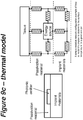
- a thermal model is needed to be developed to perform final optimisation of the results to accurately determine the surface temperature of the device as opposed to the junction temperature of the light emitter. This modelling can be performed using finite element tools such as COMSOL Multiphysics.
- a model can be built up using the LED layer materials, implant host materials and passivation cladding materials. Provided the layers are appropriately determined, the host implant should act as a heat sink to distribute heat along its bulk and then surface to prevent hot-spot development. Nevertheless this will still occur at sufficient intensities and pulse durations, necessitating this invention.
- the model itself can be built up of thermal resistive elements for the materials and their dimensions. Once created a transfer function can be developed to determine what a specific junction temperature means in terms of surface temperature.
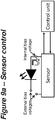
- the controller will define pulse periods for stimulus and tissue sensing. During these periods, there will be intermittent forward and reverse voltage polarities to determine the temperature during optical stimulus. Should the temperature not exceed a threshold, this will continue until the end of the tissue stimulus or sensing period. Alternatively, should the temperature exceed a defined threshold, then the control unit will stop the stimulus and a negative event logged for long term monitoring of the implant operation.
- the value of the thermal resistance for the device can be used to calculate the device surface temperature based on the measured junction temperature.
- Figure 9 shows the all steps needed to measure the junction temperature and surface temperatures and their variation.
- Figure 10 shows the simulation and experimental results for the output current of the designed CCII versus input current.
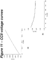
- Figure 11 shows the results for the voltage at terminal X of CCII which is expected to be 3.3V and act as reference voltage for the LED.
- the specifications achieved for CCII from simulation and experiments are almost matched and listed in Table 2.
- Figure 12 shows the frequency analysis response for the designed high gain amplifier.
- Figure 13 shows the output voltage of the amplifier versus input current of CCII where a specific load resistor is placed at the output of CCII. This voltage is linear up to 200nA for the LED reverse current.
- the specifications of the designed amplifier and overall system are listed in Table 3 and Table 4, respectively.
- the overall gain of the sensing system is about 107V/A without taking amplifier in to saturation region. For small range of temperature variations and consequently small reverse current variations a higher gain can be chosen.
- the layout of the design is depicted in Figure 14 .
- Table 3 Amplifier specifications Specifications Simulation results Gain 86 dB PM 52 ° BW 1.5kHz
- Table 4 Design specifications Specifications Simulation Results Supply voltage 5V Power dissipation 52 ⁇ A ⁇ 5V Overall gain 10 7 (V/A) Size 133 ⁇ m ⁇ 64 ⁇ m
- CMOS temperature sensor in AMS 0.35 ⁇ m CMOS technology has been designed to detect temperature variations around the implanted micro-LEDs in biomedical applications like optogenetics.
- the modeling and measurements results for GaN LEDs show that the reverse current of the LED can be considered as a reliable temperature sensitive parameter to sense thermal variations- around the LED.
- the designed CMOS temperature sensor consisting of a second generation current conveyor and a high gain amplifier is capable to receive and amplify the small current variations up to 200 nA. These current variations will then be translated into temperature variations based on the applied reverse voltage.
- This proposed method of temperature sensing is area efficient by eliminating area consuming sensing blocks which are usually used for temperature sensing in implantable systems. Also, the danger of failure because of the other devices can be decreased.
Landscapes
- Health & Medical Sciences (AREA)
- Life Sciences & Earth Sciences (AREA)
- Engineering & Computer Science (AREA)
- Biomedical Technology (AREA)
- Physics & Mathematics (AREA)
- Veterinary Medicine (AREA)
- Animal Behavior & Ethology (AREA)
- Public Health (AREA)
- General Health & Medical Sciences (AREA)
- Pathology (AREA)
- Biophysics (AREA)
- Molecular Biology (AREA)
- Surgery (AREA)
- Medical Informatics (AREA)
- Heart & Thoracic Surgery (AREA)
- Neurosurgery (AREA)
- Neurology (AREA)
- General Physics & Mathematics (AREA)
- Nuclear Medicine, Radiotherapy & Molecular Imaging (AREA)
- Radiology & Medical Imaging (AREA)
- Physiology (AREA)
- Investigating Or Analysing Materials By Optical Means (AREA)
- Investigating, Analyzing Materials By Fluorescence Or Luminescence (AREA)
Description
- The present invention relates to temperature sensors and methods of sensing temperature. The invention relates in particular, but not exclusively, to temperature sensors integrated with implantable devices.
- Implantable devices are becoming increasingly important in clinical practice. A key target area is in treating neurological deficit. For example pacemakers have been utilized since the 1950's to support proper function of cardiac muscle and have more recently been applied to the brain to treat tremor in conditions such as Parkinson's disease. Beyond neuroprosthetics there is also a need to monitor and stimulate other organs such as the Pancreas in the case of diabetes.
- Optical interrogation of cells and tissue has long been an important tool in ex-vivo studies. For example tissue staining methods have been around since the late 19th century. In the context of modern biomedical implantable devices, there are two key applications: opto-electrophysiology, and fluorescence sensing. The former allows control and recording of electrical activity in tissue. The latter can be used to explore chemical changes in cells or their environment.
- The advent of opto-genetic reporters such as green fluorescent protein in the 1990's [1] have allowed imaging of the presence (or lack of) specific cell types. More recently functional derivatives allow for the opto-genetic imaging of cellular function and in particular, electrical funciton. For example, Ohiem et al. [2] have developed a red-fluorescent optogenetic calcium indicator which can be genetically inserted into cells to determine the level of calcium function. Calcium is an important chemical in many cellular processes and can be used to interrogate both the relative level of activity of neuron cells and more subtle biochemical changes in many cell types. Chemical reporters also exist, but these are less desirable as they would need to be continuously infused either because the optically active proteins bleach, or because ligand molecule which attaches them to the target cell breaks. In contrast genetically encoded reporters are continuously produced/recycled by their host cells.
- In addition to optical recording, optical stimulus is possible through optogentic and optochemical methods. Traditional optochemical methods have utilized cage structures around a bio-active initiator molecules e.g. caged glutamate. In such structures, ltraviolet light is used to uncage the active part of the molecule and thus biomchemically activate the target cell (e.g. Shoham et al. [3]). This is problematic in-vivo so more recent methodologies have utilized lock and key approaches with photoconformable molecules. E.g. Broichhagen et al. utilize such approaches to insulin secretion [4]. However, perhaps the most useful method is optogenetics. In this case, cells are genetically modified to continuously produce optically sensitive proteins. Thus, there is no subsequent need to pump continuous biochemicals into the body. Such optogenetic stimulation can use either channelrhodospsins - light sensitive cation channels [5], halorodopsins - light sensitive ion pumps [6], or melanopsins - light sensitive G-protein coupled receptor systems [7]. Each has their own relative advantages and a good review of the field has be written by J. Barrett et al. [8]. What is common to all of these approaches is that they require high intensity irradiation of the optical targets. Furthermore the fundamental optically active cores in all of these proteins are derived from conjugated small molecules which are optically active in the ultraviolet (350nm to orange/red 600nm) region of the electromagnetic spectrum. In particular, blue wavelengths in this range are heavily scattered by neural tissue. This means there is a requirement for light delivery in close proximity to these targets. This can be achieved by one of two methods:
- 1. Light can be generated at some distance and then guided to the local position using optical confinement (e.g. optic fibre or waveguide) until the point of delivery.
- 2. Light can be produced locally by a penetrating or otherwise implantable device incorporating a microphotonic element close to the required target.
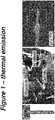
- Each of these approaches has its relative advantages and disadvantages. In the case of optical delivery to the target, it can be challenging to multiplex large numbers of independent signals in a single system. Furthermore the light generator will still be implantable and will still generate heat, albeit perhaps from a domain than can better tolerate thermal load. In the case of microphotonic generation close to the target, the key issue is the formation of localized hot spots close to the biomedical device surface. A demonstration of such a hotspot can be seen in
Figure 1 , which shows hot spot formation in implantable optrodes. On the left: an implantable optrode which is capable of delivering both optical emission and electrical recording. In the centre: a testing methodology in air utilising photodiode and infra-red camera. On the right: the temperature increase if two of the incorporated micro-LEDs are illuminated continuously. - Clearly, if implantable microphotonic components are illuminated at high radiance, there is the potential for significant heating at the device surface. However, for chronic implants, the raising of ambient temperature in surrounding tissue is undesirable. The current literature is not entirely clear on what long term effects could result from such temperature increase. What is known is that beyond 5OC irreversible damage is done in acute experiments [9]. Additionally, as temperature raises beyond 1OC signaling in the surrounding neural cells may be affected. The human body undergoes regular illness and recovery cycles within which fevers raise body temperatures by a few degrees with no long term ill-effect. However, even at the best of circumstances, there is typically some scar tissue formation around long term implants. This could be worsened by temperature increases. Furthermore raised surface temperatures on biomedical implants could engender inflammatory responses. In turn long term inflammatory responses have been linked to genetic mutations and tumor formations.
- So clearly it would be desirable to monitor device temperatures and ensure they are maintained within desirable limits (e.g. T<39C, dT < 2C above ambient).
- There are a number of configurations for illuminating target tissue from photonic implants, as shown in
Figure 2 . The use depends on the target application. For nerve bundles, cuff style optrodes which can wrap around the bundle are more appropriate (Figure 2a ). For direct stimulation of tissue from the surface, a planar structure is more appropriate (Figure 2b ). For deep penetration of tissue, penetrating optrodes either in single (Figure 2c ) or in array formation are most appropriate (Figure 2d ). - On-chip temperature sensors have been used to monitor human health for diseases diagnosis and treatment. For example, the adaptive multi-sensor CMOS system proposed by Huang et al. [10] comprises different on-chip sensors including temperature sensor. This device is capable of body temperature sensing from 32OC to 42OC and also environmental temperature sensing outside the body from -20OC to 120OC. Lee et al. presented a low-cost CMOS thermal sensor chip for biomedical application to monitor temperature from 33O C to 42OC with less than 0.15 OC inaccuracy [11]. In their work, bipolar transistors are used to sense temperature and generate the needed reference voltage for sigma-delta analog to digital converter. Crepaldi et al proposed a low power CMOS based front-end thermal sensing element with 0.24 OC inaccuracy suitable for biomedical application [12].
- The downside of using additional sensors is that they take additional surface space and need additional address architectures. This may thus present difficulties to integration. Furthermore, it increases the complexity and thus cost of fabrication. Perhaps most significantly by having separate sensors for temperature, there is always a danger that failure in the sensor may provide inaccurate readings; perhaps stating that the temperature rise is limited when the opposite is the case.
- It is known in the art from
US 2007/075370 A1 , that diodes can measure temperatures on a microprocessor belonging to a computer (e.g. die temperature or DieTemp), and methods can sense temperatures on a microprocessor by measuring the current through existing Electrostatic discharge (ESD) devices. It is known in the art fromUS 2015/117494 A1 , that such diodes can have a more refined sensitivity or accuracy by implementing a "digital circuit" (or control logic) that compares a charge voltage of a capacitor to pre-set upper and lower thresholds. It is also known in the art from Dehkhoda et al. ("Smart Optrode for Neural Stimulation and Sensing", Imperial College London, 2015) that electronic circuits may be incorporated directed onto implantable devices in order to determine a diagnostic state. - In general terms, the present invention proposes to use a light emitter (e.g. a microphotonic component such as a micro LED or laser diode) itself as its own thermal sensor. By utilizing the emitter as its own temperature sensor, the continued functionality of the device is intrinsically linked to its self-diagnosis.
- In general terms we present a method to determine the temperature of microphotonic medical implants. The proposal is to use the photonic emitter as its own sensor and develop readout circuitry and models to accurately determine the surface temperature of the device. There are two primary classes of applications where microphotonics could be used in implantable devices; opto-electrophysiology, and fluorescence sensing. In opto-electrophysiology, optical methods such as optogenetics are used to provide optical stimulus and/or optical recording of cellular electrical activity. In Fluorescence sensing -the biochemical environment is optically probed with either fluorescence reporter proteins or via cellular autofluorescent signatures. In such scenarios light needs to be delivered to the nervous tissue. The optically sensitive proteins used in such applications typically tend to be sensitive in the photonic region of UV (350mm) to red (600nm). In this region scattering processes dominate optical traversal of tissue and thus light delivery systems need to be utilized. One key form of such a system is to generate light directly, but this can cause localized heating effects at the device surface which may need to be monitored. This invention allows such monitoring utilizing the heat producing device itself as a sensor, combined with specific electronic control and signal post-processing.
- In a first aspect the invention provides a temperature sensor for medical use comprising:
- a microphotonic light emitter comprising a junction between two materials;
- an electrical circuit for applying a reverse bias voltage across the light emitter and for measuring a reverse current; and
- means for calculating a temperature from the measured reverse current;
the temperature sensor being characterised in that;
the electrical circuit comprises a second generation current conveyor, CCII, configured for maintaining the reverse bias voltage within +/- 5% of a target bias. - The means for calculating a temperature from the measured reverse current may include a predefined correlation of reverse current versus temperature for the light emitter.
- The temperature that is calculated may be a junction temperature of the light emitter or a surface temperature of the light emitter, for example. In the case where the temperature is surface temperature of the light emitter, it may be calculated, for example, using a model that relates surface temperature to the junction temperature of the light emitter (where that is calculated first) or directly to the measured reverse current. The model parameters will typically be determined by the implant mass and thermal properties relative to the passivation material. As an alternative example, the surface temperature may be calculated using a transfer function to determine the surface temperature based on a current/voltage measurement from the light emitter.
- In some embodiments, the electrical circuit is configured to maintain the bias voltage at a constant value between 0 and 5V in reverse bias across the optical device.
- In some embodiments, the light emitter is, for example a light emitting diode or a stimulated emission device such as a semiconductor laser diode (e.g. in the form of a vertical cavity surface emitting laser). It may be formed, for example in Gallium Nitride, Silicon Carbide, Aluminum Nitride, Indium Nitride, Gallium Phosphide, Aluminium Phosphide, Zinc Sulphide, Magnesium sulphide, Magnesium selenide, or Zn Selenide.
- In some embodiments, the electrical circuit comprises one or more low pass filters to filter switching noise, whereby the photonic device temperature can be accurately determined despite variations in power supply noise.
- In some embodiments, the light emitter has two modes of operation, a temperature sensing mode when a reverse bias voltage is applied across the light emitter and a light emission mode when a forward bias voltage is applied across the light emitter. The temperature sensor may be controlled to switch back and forth between the temperature sensing mode and the light emitting mode at a predefined frequency, for example from 1GHz to 10Hz. High frequencies (e.g. 1MHz - 1GHz) typically encompass short pulses (e.g. Ins - 1µs), useful for instance for fluorescence lifetime sensing measurements of tissue. Low frequencies (e.g. 10hz - 1MHz) typically encompass longer pulses (e.g. 100ms - 1µs) useful for instance for optical (primarily neural) tissue stimulation.
- In some embodiments, the temperature sensor can additionally be switched to an off mode in which no voltage is applied across the light emitter.
- In some embodiments, the temperature sensor includes a controller for switching the temperature sensor between modes. The controller may, for example be configured (e.g. programmed) to switch the temperature sensor between modes at defined time points, pulse widths and/or repetition frequencies. The controller may additionally or alternatively be configured to stop subsequent operation in the light emission mode if the calculated temperature exceeds a predefined threshold. The predefined threshold may, for example, be in the range 0.1 to 3C above the ambient temperature of the tissue.
- In some embodiments, the forward bias voltage is in the range 1.5V - 10V. Typically the selected forward bias will depend on the light requirement and optical wavelength. Shorter wavelengths generally need higher bias, as do higher intensities.
- In some embodiments, the current in the forward bias is between 1uA to 50mA, dependent on the microphotonic size and required radiant density.
- In a second aspect, the invention provides an implantable biomedical device incorporating a temperature sensor as outlined above.
- The device is for optogenetic stimulus of nervous function, wherein the light emitter of the temperature sensor performs optogenetic stimulus when the light emitter is in the light emission mode. In the light emission mode the light emitter of the temperature sensor may perform optogenetic stimulus of electrical activity or chemical activity indirectly via opto-electrical stimulus in non-nervous cells and/or tissue. The device may be operable to record cellular electrical or calcium potential in nervous and/or non-nervous tissue.
- The invention proposes use of the temperature sensor to measure temperature by applying the reverse bias across the microphotonic light emitter, measuring the reverse current and calculating the temperature from the measured reverse current.
- An embodiment of the invention is described below with reference to the accompanying figures, in which:
-
Figure 1 shows hot spot formation in implantable optrodes. Left an implantable optrode which is capable of delivering both optical emission and electrical recording. Centre a testing methodology in air utilising photodiode and infra-red camera. Right the temperature increase if two of the incorporated the micro-LEDs are illuminated continuously; -
Figure 2 shows Formats of optical interrogation of neural tissue (a) cuff optrode (b) planar surface emitting optrode array (c) penetrating singular optrode (d) penetrating optrode array; -
Figure 3 shows Measurement results achieved for GaN LED (a) absolute reverse current versus temperature in different bias voltages and (b) revers current versus voltage in different temperatures. Note how the reverse current increases much more significantly with reverse bias; -
Figure 4 shows Multiple quantum well architecture of LEDs and VCSEL lasers (a) band diagram without doping (b) band diagram with doping; -
Figure 5 shows (a) Active optrode including temperature sensor and (b) Exemplar penetrating biomedical device for applications in central nervous tissue; -
Figure 6 is a Block diagram of the proposed temperature sensor; -
Figure 7 is an Exemplar embodiment of the sensing architecture at a transistor level; -
Figure 8 (a) is a block diagram of the LED employment for light emission and temperature sensing functions; andfigure 8 (b) is timing diagram of the applied signals to the LED for light emission and temperature sensing; -
Figures 9(a) and9(b) schematically show the approach to sensor control andfig. 9c show a temperature model; -
Figure 10 shows Current gain of the designed CCII (Iz/Ix). The designed CCII should deliver the received current to its output with a linear gain in a wide range of input current (a) simulation results (b) experimental results -
Figure 10 shows Current gain of the designed CCII (Iz/Ix). The designed CCII should deliver the received current to its output with a linear gain in a wide range of input current (a) simulation results (b) experimental results; -
Figure 11 shows Voltage of terminal X in CCII (Vx) which is used as reference voltage, 3.3V to bias the LED at its anode (a) simulation results (b) experimental results; -
Figure 12 shows Frequency analysis response for the amplifier in the last stage of the sensor with high gain; -
Figure 13 shows amplifier output for a specific CCII load versus input current of CCII; and -
Figure 14 Layout of the designed temperature sensor including bias circuit, CCII and amplifier. - There are two primary forms of microphotonic emitters that could be used for useful optical interrogation of biological tissue:
- 1. Micro-sized light emitting diodes, primarily those utilising multi-quantum well (MQW) structures to ensure high efficiency optical emission.
- 2. Micro-sized stimulated emission devices i.e. lasers, with the most promising candidates being vertical cavity surface emitting lasers.
- The optically active core material of these emitters could comprise of Gallium Nitride, Silicon Carbide, Aluminum Nitride, Indium Nitride, Gallium Phosphide, Aluminium Phosphide, Zinc Sulphide, Magnesium sulphide, Magnesium Selenide, or Zn Selenide depending on the desired optical properties. An example of the use of Gallium Nitride diodes for optical interrogation of astrocyte tissue can be seen in Berlinguer et al [13].
- Vertical cavity surface emitting lasers are still in their infancy. Recent examples include a recent VCSEL developed by Wen-Jie Liu at Xiamen University [14]. Such devices are still in their infancy, but at their core is a fundamentally similar semiconductor structure to the light emitting diode. As the charge generation and current flow in all diodes is temperature dependent they may be used to detect the junction temperature, and from there infer the surface temperature of a given device.
- In forward bias the LED current will exponentially increase with voltage. The current levels are thus high and will result in light emission (and thermal emission). Thus, from the perspective of diagnostics switching the diode into reverse bias allows interrogation of current level within a specific voltage domain. Currents in the reverse bias case are low and do not lead to perceptible light emission under normal voltages.
Figure 3 shows the results achieved from a standard Gallium Nitride micro-LED incorporating a multiple quantum well architecture. The reverse current of such LEDs change linearly with temperature for a fixed bias voltage (Figure 3a ), but exponentially with reverse bias (Figure 3b ). - At a first approximation, an LED per definition is a light emitting diode. The diode structure consists of p and n doped layers which are combined in a p-n junction structure. The Shockley equation for a p-n junction given by (1) is used to derive the temperature dependency of the reverse current.


- Here, A is the cross-sectional area of the p-n junction; Dn and Dp are diffusion constants for electrons and holes exhibiting a T-1/2 temperature dependency; τn and τp are the minority carrier lifetimes for electrons and holes supposed to be temperature independent; ND and NA are doping concentration of donors and acceptors which are independent of temperature; Nc and Nv are effective densities of states at the conduction-band and valence-band with temperature dependency of T3/2. Eg is the energy bandgap given by:

- In practice the theoretical framework of LEDs is more complex. Fundamentally, LEDs generate light by electron-hole recombination. Thus, the efficiency of light generation is a result of the percent of injected current (electrons and holes) which recombine to give our light compared to those that continue to the opposite terminal or recombine non-radiatevely. As a result, LED designers create a multiple quantum well structure with multiple layers of materials of different bandgaps to create trapping centres for recombination.
- A quantum well is a heterostructure with one thin well layer surrounded by two barrier layers. Both electrons and holes are confined in the well layer which is so thin about 40 atomic layers. The quantum wells can be grown using molecular beam epitaxy (MBE) [17], and metal-organic chemical vapor deposition (MOCVD) [18]. The typical materials to be grown can be any sequence of GaAs, AlAs, and AlGaAs. The multiple quantum well layers act as trapping centres for charge mobility. Escape from such traps is therefore mediated primarily by thermionic emission and quantum tunnelling (
Figure 4 ) over the traps. Both effects are temperature dependent [15, 19] resulting in a linear dependency within the temperature range interesting to this invention. - To summarize: Based on
Figure 3 , it is very challenging to determine the junction temperature of an LED in reverse bias because the current rises considerably faster due to variations in bias than variations in temperature. Thus to achieve effective functionality, the LED must be interrogated at a fixed reverse bias which does not deviate in time or due to noise. Furthermore, although the light emitter will typically be close to the surface, what is being measured is the junction temperature rather than the surface temperature itself. A thermal model of how the LED sits in the host system must therefore be used to provide further accuracy in determining the surface temperature. -
Figure 5 shows a single penetrating optrode with inbuilt stimulation and recording circuits along its shaft. The LED based temperature sensor circuitry is placed close to the µLEDs to be easily operating in antiphase with optical emission. - As the reverse current of LED is employed as temperature sensitive parameter to design the sensor we have experimentally explored GaN LEDs performance to investigate the linear relationship between junction temperature (Tj) and reverse current [15].
- An LED test setup is implemented using GaN LED to extract the needed IR-T curve at different bias voltages. The LED under test is placed in an isolated dark box to guarantee that the measured current is only due to the temperature change. The box is also temperature isolated to ensure about the accuracy of the measured temperature. A hot plate is placed under the LED to increase the temperature which can be measured and recorded by the IR Optris PI camera and the camera interface software, respectively.
- In a fixed reverse bias voltage across the LED, temperature is increased using the hot plat from 28°C to 60°C and the reverse current is measured. The measurement has been repeated for different bias voltages from -1.0V to -2.2V.
- The results achieved from the LED testing experiment are shown in
Figure 3 . The reverse current of LED is changing linearly with temperature for a fixed bias voltage. On the other hand, the reverse current changes with voltage in a fixed temperature. In other word, a variant or temperature dependent bias voltage can cause a large reverse current variation which is not purely related to temperature variation. As a result the designed temperature sensor should provide a fixed temperature independent bias voltage for the LED to avoid current variation because of bias voltage variation. -
Figure 6 depicts the block diagram of the proposed temperature sensing system based on LED. The designed sensing system measures the reverse current of the LED which is reversely biased using a bias voltage. Temperature variation linearly changes this reverse current if a fixed bias voltage is applied across the LED. The bias voltage must be precise and temperature independent not to contribute in reverse current changing because the reverse current can change with bias voltage significantly. Therefore, a circuit is needed to provide the bias voltage across the LED and receive its current in same time. For this purpose, a second generation current conveyor (CCII) is used at the first stage of the sensor which is capable of providing a precise bias voltage at the input (X) while receiving current using the same input terminal. In other word, CCII conveys the received current from LED to the output (Z).. The CCII receives an external bias voltage in other input (Y) and copies this voltage on the input (X) which is supposed to be connected to LED and receive the reverse current.. In this design VX is match to VY and the output current should follow the current at the input (X). - A unity current gain for a range of frequencies is needed for the CCII to accurately translate the current changes to temperature variation in the next stages. Also, linearity is important for a specific input range of reverse current. Therefore, a robust bias voltage, unity current gain, linearity and low power are the most important specifications in designing the CCII.
- A resistor is used to convert the CCII out current to voltage to be amplified using the amplifier in the last stage. The designed amplifier is a single input single output high gain amplifier. This amplifier receives the current variation as voltage in the input and amplifies that to a large signal suitable to digitize using ADC.
- The most important parameters in the design of this amplifier are high gain, low power, high dynamic range, high CMRR and PSRR. The common mode rejection properties are determined by matching of transistors and in particular, matching at the input differential stage. This is achieved through enlarging transistors and performing Monte Carlo modelling at the design stage to ensure a probabilistic match. Similarly, the use of larger transistors supports the low pass filtering to reject high frequency power supply noise. A negative feedback loop is utilised to support high gain and thermal noise rejection.
- An exemplar of our designed sensor was created using a standard CMOS (Complementary Metal Oxide Semiconductor) process from Austra Microsystems. The technology node was 0.35 µm and standard CAD/EDA tools were utilised for its design. The schematic of the design is shown in
Figure 7 . The CCII at first stage receives the LED current in terminal X which has the same vdd voltage as input Y. The received current is copied to the output Z connected to a resistive load [20]. The second stage includes a two-stage high gain amplifier. - The sensor circuitry is placed close to the LED which is easily operating in antiphase with optical emission done using stimulation circuits. Temperature sensing is supposed to be performed after LED light emission. In other word, forward biased LED emits light where its intensity can be controlled using pulse width modulation. Then, switching the LED in to the sensor path provides reverse bias for the LED using a specific voltage reference (
Figure 8 ). - Table 1 lists different examples for LED timing operation. PW1 is used to stimulate the LED by providing the forward bias. After this operation, temperature sensing will be performed to sense the temperature around the LED and its variation by operating in different time slots after LED stimulation.
- Stimulation duration (PW1) should be enough to do the LED stimulation and provide the required light intensity. Therefore, PW1 is chosen based on the applied signal as bias to the LED, its specification and the required light intensity. Sensor operation time (PW2) should be enough to do temperature sensing operation and in same time small enough to decrease the overall power consumption in the system as the amplifier of the sensor is the most power consuming part of the design.
Table 1 exemplar timing operation for stimulating the LED with PW1 and then sensing the temperature with PW2 Frequency (Hz) T (msec) PW1 (msec) Duty cycle1 PW2 (msec) Duty cycle2 5 200 10 5% 2 1% 10 100 10 10% 2 2% - The proposed senor measures the LED junction temperature. A thermal model is needed to be developed to perform final optimisation of the results to accurately determine the surface temperature of the device as opposed to the junction temperature of the light emitter.
This modelling can be performed using finite element tools such as COMSOL Multiphysics. A model can be built up using the LED layer materials, implant host materials and passivation cladding materials. Provided the layers are appropriately determined, the host implant should act as a heat sink to distribute heat along its bulk and then surface to prevent hot-spot development. Nevertheless this will still occur at sufficient intensities and pulse durations, necessitating this invention. The model itself can be built up of thermal resistive elements for the materials and their dimensions. Once created a transfer function can be developed to determine what a specific junction temperature means in terms of surface temperature. - Once implemented on the control unit. The controller will define pulse periods for stimulus and tissue sensing. During these periods, there will be intermittent forward and reverse voltage polarities to determine the temperature during optical stimulus. Should the temperature not exceed a threshold, this will continue until the end of the tissue stimulus or sensing period. Alternatively, should the temperature exceed a defined threshold, then the control unit will stop the stimulus and a negative event logged for long term monitoring of the implant operation.
- The value of the thermal resistance for the device can be used to calculate the device surface temperature based on the measured junction temperature.
Figure 9 shows the all steps needed to measure the junction temperature and surface temperatures and their variation. -
Figure 10 shows the simulation and experimental results for the output current of the designed CCII versus input current.Figure 11 shows the results for the voltage at terminal X of CCII which is expected to be 3.3V and act as reference voltage for the LED. The specifications achieved for CCII from simulation and experiments are almost matched and listed in Table 2.Table 2 Design specifications for CCII Specifications @ Ix=0∼200nA Simulation results Experimental results Current gain 1 1 Vx/Vy 3.299/3.3 3.275/3.3 -
Figure 12 shows the frequency analysis response for the designed high gain amplifier.Figure 13 shows the output voltage of the amplifier versus input current of CCII where a specific load resistor is placed at the output of CCII. This voltage is linear up to 200nA for the LED reverse current. - The specifications of the designed amplifier and overall system are listed in Table 3 and Table 4, respectively. The overall gain of the sensing system is about 107V/A without taking amplifier in to saturation region. For small range of temperature variations and consequently small reverse current variations a higher gain can be chosen. The layout of the design is depicted in
Figure 14 .Table 3 Amplifier specifications Specifications Simulation results Gain 86 dB PM 52° BW 1.5kHz Table 4 Design specifications Specifications Simulation Results Supply voltage 5V Power dissipation 52µA×5V Overall gain 107 (V/A) Size 133µm×64µm - An LED-based temperature sensor in AMS 0.35 µm CMOS technology has been designed to detect temperature variations around the implanted micro-LEDs in biomedical applications like optogenetics. The modeling and measurements results for GaN LEDs show that the reverse current of the LED can be considered as a reliable temperature sensitive parameter to sense thermal variations- around the LED. The designed CMOS temperature sensor consisting of a second generation current conveyor and a high gain amplifier is capable to receive and amplify the small current variations up to 200 nA. These current variations will then be translated into temperature variations based on the applied reverse voltage. This proposed method of temperature sensing is area efficient by eliminating area consuming sensing blocks which are usually used for temperature sensing in implantable systems. Also, the danger of failure because of the other devices can be decreased.
-
- [1] R. Heim, A. B. Cubitt and R. Y. Tsien, "Improved green fluorescence," Nature, vol. 373, no. 6516, pp. 663-4, 1995.
- [2] m. Oheim M, M. van 't Hoff, A. Feltz and A. Zamaleeva, "New red-fluorescent calcium indicators for optogenetics, photoactivation and multi-color imaging," vol. 1843, no. 10, pp. 284-306, 2014.
- [3] S. Shoham , D. H. O'Connor, D. V. Sarkisov D V and S. S. Wang, "Rapid neurotransmitter uncaging in spatially defined patterns," Nature methods, vol. 2, pp. 837-843, 2005.
- [4] J. Broichhagen, T. Podewin, H. Meyer-Berg, Y. von Ohlen, N. R. Johnston, B. J. Jones, S. R. Baloom, G. A. Rutter, A. Hoffmann-Roder and D. Hodson, "Optical Control of Insulin Secretion Using an Incretin Switch," Angewandte Chemie International Edition, vol. 54, 2015.
- [5] G. Nagel, T. Szellas, W. Huhn, N. Kateriya, N. Adeishvili and P. Berthold, "Channelrhodopsin-2, a directly light-gated cation-selective membrane channel," National Academy of Science, vol. 100, pp. 13940-13945, 2003.
- [6] F. Zhang, L. Wang, M. Brauner, J. Liewald J, K. Kay, N. Watzke, P. Wood, E. Bamberg, G. Nagel, A. Gottschalk and K. Deisseroth, "Multimodal fast optical interrogation of neural circuitry," Nature, vol. 446, no. 7136, p. 633-639, 2007.
- [7] A. Koizumi, K. Tanaka KF and A. Yamanaka, "The manipulation of neural and cellular activities by ectopic expression of melanopsin," Neuroscience Research, vol. 75, no. 1, pp. 3-5, 2013.
- [8] J. Barrett, R. Berlinguer-Palmini and P. Degenaar, "Optogenetic approaches to retinal prosthesis," Visual Neuroscience, vol. 31, no. 4-5, pp. 345-354, 2014.
- [9] T. Fujii and Y. Ibata, "Effects of heating on electrical activities of guinea pig olfactory cortical slices," European Jurnal of Physiology, vol. 392, no. 3, p. 257-260, 1982.
- [10] Y. J. Huang, T. H. Tzeng, T. W. Lin and C. W. Huang, "A Self-Powered CMOS Reconfigurable Multi-Sensor," IEEE Journal of Solid-State Circuits, vol. 49, no. 4, pp. 851-866, 2014.
- [11] H. Y. Lee, C. M. Hsu and C. H. Luo, "CMOS thermal sensing system with simplified circuits and high accuracy for biomedical application Circuits and Systems," in Proceedings of IEEE International Symposium on Circuits and Systems, ISCAS, 2006.
- [12] P. C. Crepaldi, R. L. Moreno and T. C. Pimenta, "Low-voltage, low-power, high linearity front-end thermal sensing element," Electronics Letters, vol. 46, no. 18, pp. 1271-1272, 2010.
- [13] R. Berlinguer-Palmini, R. Narducci, K. Merhan, A. Dilaghi, F. Moroni, A. Masi, T. Scartabelli, E. Landucci, M. Sili, A. Schettini, B. McGovern B and G. Mannaioni, "Arrays of MicroLEDs and Astrocytes: Biological Amplifiers to Optogenetically Modulate Neuronal Networks Reducing Light Requirement," PLoS One, vol. 9, no. 9, 2014.
- [14] e. a. Liu, Applied Physics Letters, vol. 104, no. 251116, 2014.
- [15] B. Wu, S. Lin, T. M. Shih, Y. Gao, Y. Lu, L. Zhu, G. Chen and Z. Chen, "Junction-Temperature Determination in InGaN Light-Emitting Diodes Using Reverse Current Method," IEEE Transaction on Electronc Devices, vol. 60, no. 1, 2013.
- [16] Y. Xi and E. F. Schubert, "Junction-temperature measurement in GaN ultraviolet light-emitting diodes using diode forward voltage method," APPLIED PHYSICS LETTERS, vol. 85, no. 12, pp. 2163-2165, 2004.
- [17] A. Y. Cao, "Advances in molecular beam epitaxy (MBE)," Journal of Crystal Growth, vol. 111, no. 1, pp. 1-13, 1991.
- [18] K. Furuya and Y. Miyamoto, "GaInAsP/InP organometallic vapor phase epitaxy for research and fabrication of devices," International Journal of High Speed Electronics, vol. 1, no. 347, 1990.
- [19] X. A. Cao, E. B. Stokes and P. M. Sandvik, "Diffusion and Tunneling Currents in GaN/InGaN Multiple Quantum Well Light-Emitting Diodes," IEEE ELECTRON DEVICE LETTERS, vol. 23, no. 9, 2002.
- [20] S. B. Salem, M. Fakhfakh, D. S. Masmoudi, M. Loulou, P. Loumeau and N. Masmoudi, "A High Performances CMOS CCII and High Frequency Application," Analog Integrated Circuits and Signal Processing, vol. 49, pp. 71-78, 2006.
Claims (13)
- A temperature sensor for medical use comprising:a microphotonic light emitter comprising a junction between two materials;an electrical circuit for applying a reverse bias voltage across the light emitter and for measuring a reverse current; andmeans for calculating a temperature from the measured reverse current;
the temperature sensor being characterised in that;
the electrical circuit comprises a second generation current conveyor, CCII, configured for maintaining the reverse bias voltage within +/- 5% of a target bias. - A temperature sensor according to claim 1, wherein the means for calculating a temperature from the measured reverse current includes a predefined correlation of reverse current versus temperature for the light emitter; and wherein the temperature that is calculated is a junction temperature of the light emitter or a surface temperature of the light emitter, wherein the surface temperature is calculated using a model that relates surface temperature to the junction temperature of the light emitter and/or to the measured reverse current.
- A temperature sensor according to claim 2, wherein the surface temperature is calculated using a transfer function to determine the surface temperature based on a current/voltage measurement from the light emitter; and/or wherein said electrical circuit is configured to maintain the bias voltage at a constant value between 0 and 5V in reverse bias across the optical device.
- A temperature sensor according to any one of the preceding claims, wherein the light emitter is a light emitting diode, a stimulated emission device, or a semiconductor laser diode.
- A temperature sensor according to any one of claims 1 to 4, wherein the light emitter is formed in Gallium Nitride, Silicon Carbide, Aluminum Nitride, Indium Nitride, Gallium Phosphide, Aluminium Phosphide, Zinc Sulphide, Magnesium sulphide, Magnesium selenide, or Zn Selenide.
- A temperature sensor according to any one of the preceding claims, wherein the electrical circuit comprises one or more low pass filters to filter switching noise, whereby the photonic device temperature can be accurately determined despite variations in power supply noise.
- A temperature sensor according to any one of the preceding claims, in which the light emitter has two modes of operation, a temperature sensing mode when a reverse bias voltage is applied across the light emitter and a light emission mode when a forward bias voltage is applied across the light emitter; and wherein the temperature sensor is controlled to switch back and forth between the temperature sensing mode and the light emitting mode at a predefined frequency; and wherein said predefined frequency is from 1GHz to 10Hz.
- A temperature sensor according to claim 7, wherein the temperature sensor can additionally be switched to an off mode in which no voltage is applied across the light emitter.
- A temperature sensor according to claim 8, comprising a controller for switching the temperature sensor between modes; and wherein the controller is configured to switch the temperature sensor between modes at defined time points, pulse widths and/or repetition frequencies.
- A temperature sensor according to claim 9, wherein the controller is configured to stop subsequent operation in the light emission mode if the calculated temperature exceeds a predefined threshold wherein the predefined threshold is in the range 0.1 to 3C above the ambient temperature of the tissue.
- A temperature sensor according to claim 10, wherein the forward bias voltage is in the range 1.5V - 10V; and/or wherein the current in the forward bias is between 1uA to 50mA.
- An implantable biomedical device for optogenetic stimulus of nervous function, the device incorporating a temperature sensor according to any one of the preceding claims;
wherein the light emitter of the temperature sensor performs optogenetic stimulus of electrical activity or chemical activity indirectly via opto-electrical stimulus in non-nervous cells and/or tissue, when the light emitter is in the light emission mode;
and is operable to record cellular electrical or calcium potential in nervous and/or non-nervous tissue. - Use of the temperature sensor according to claim 1 to measure temperature by applying the reverse bias across the microphotonic light emitter, measuring the reverse current and calculating the temperature from the measured reverse current.
Applications Claiming Priority (2)
| Application Number | Priority Date | Filing Date | Title |
|---|---|---|---|
| GBGB1522790.3A GB201522790D0 (en) | 2015-12-23 | 2015-12-23 | Temperature sensor |
| PCT/EP2016/082433 WO2017109103A1 (en) | 2015-12-23 | 2016-12-22 | Temperature sensor |
Publications (2)
| Publication Number | Publication Date |
|---|---|
| EP3394581A1 EP3394581A1 (en) | 2018-10-31 |
| EP3394581B1 true EP3394581B1 (en) | 2020-12-02 |
Family
ID=55311556
Family Applications (1)
| Application Number | Title | Priority Date | Filing Date |
|---|---|---|---|
| EP16822172.9A Active EP3394581B1 (en) | 2015-12-23 | 2016-12-22 | Temperature sensor |
Country Status (4)
| Country | Link |
|---|---|
| US (1) | US11015986B2 (en) |
| EP (1) | EP3394581B1 (en) |
| GB (1) | GB201522790D0 (en) |
| WO (1) | WO2017109103A1 (en) |
Families Citing this family (13)
| Publication number | Priority date | Publication date | Assignee | Title |
|---|---|---|---|---|
| US10335607B2 (en) | 2016-02-05 | 2019-07-02 | Boston Scientific Neuromodulation Corporation | Implantable optical stimulation lead and methods of making and using |
| EP3254636B1 (en) * | 2016-06-07 | 2019-07-24 | Braun GmbH | Skin treatment device |
| WO2018089931A1 (en) * | 2016-11-14 | 2018-05-17 | The Charles Stark Draper Laboratory Inc. | Compliant optrodes for monitoring and stimulating biological tissue with patterned light |
| US10874876B2 (en) * | 2018-01-26 | 2020-12-29 | International Business Machines Corporation | Multiple light sources integrated in a neural probe for multi-wavelength activation |
| EP3586916A1 (en) * | 2018-06-25 | 2020-01-01 | BIOTRONIK SE & Co. KG | Device for activating of cell structures by means of electromagnetic energy |
| WO2020102039A1 (en) | 2018-11-16 | 2020-05-22 | Boston Scientific Neuromodulation Corporation | An optical stimulation system with on-demand monitoring and methods of making |
| US20220074795A1 (en) * | 2018-12-25 | 2022-03-10 | Ozyegin Universitesi | System for measuring junction temperature of photonics devices |
| CN109645978B (en) * | 2019-01-29 | 2021-02-23 | 北京大学 | Brain probe reading circuit |
| CN109855749A (en) * | 2019-04-02 | 2019-06-07 | 深圳市思坦科技有限公司 | A kind of temperature measuring device and measurement method |
| EP4288145B1 (en) | 2021-04-08 | 2025-01-15 | Boston Scientific Neuromodulation Corporation | Photobiomodulation system and delivery device |
| CN114741836B (en) * | 2022-02-15 | 2025-08-15 | 杭州电子科技大学 | GaN HEMT direct current I-V temperature model building method |
| US20240058619A1 (en) * | 2022-08-22 | 2024-02-22 | Boston Scientific Neuromodulation Corporation | Implantable photobiomodulation systems employing thermal monitoring or control and methods of making and using |
| EP4398258A3 (en) | 2023-01-04 | 2024-08-28 | Boston Scientific Neuromodulation Corporation | Systems and methods incorporating a light therapy user interface for optical modulation |
Family Cites Families (8)
| Publication number | Priority date | Publication date | Assignee | Title |
|---|---|---|---|---|
| US5445608A (en) * | 1993-08-16 | 1995-08-29 | James C. Chen | Method and apparatus for providing light-activated therapy |
| US10052497B2 (en) * | 2005-07-22 | 2018-08-21 | The Board Of Trustees Of The Leland Stanford Junior University | System for optical stimulation of target cells |
| US7519498B2 (en) * | 2005-10-04 | 2009-04-14 | International Business Machines Corporation | Thermal sensing method and apparatus using existing ESD devices |
| TWI404923B (en) | 2008-07-07 | 2013-08-11 | Ind Tech Res Inst | Standard Test Method for PN Joint Temperature of Light Emitting Diodes |
| US20110125078A1 (en) * | 2009-11-25 | 2011-05-26 | Medtronic, Inc. | Optical stimulation therapy |
| GB201121874D0 (en) | 2011-12-20 | 2012-02-01 | Mled Ltd | Integrated medical device |
| EP3659518A1 (en) * | 2012-11-21 | 2020-06-03 | Circuit Therapeutics, Inc. | System and method for optogenetic therapy |
| US9709445B2 (en) * | 2013-10-25 | 2017-07-18 | Stmicroelectronics S.R.L. | Temperature sensor and related method |
-
2015
- 2015-12-23 GB GBGB1522790.3A patent/GB201522790D0/en not_active Ceased
-
2016
- 2016-12-22 EP EP16822172.9A patent/EP3394581B1/en active Active
- 2016-12-22 US US16/065,660 patent/US11015986B2/en not_active Expired - Fee Related
- 2016-12-22 WO PCT/EP2016/082433 patent/WO2017109103A1/en not_active Ceased
Non-Patent Citations (3)
| Title |
|---|
| BIQING WU ET AL: "Junction-Temperature Determination in InGaN Light-Emitting Diodes Using Reverse Current Method", IEEE TRANSACTIONS ON ELECTRON DEVICES, IEEE SERVICE CENTER, PISACATAWAY, NJ, US, vol. 60, no. 1, 1 January 2013 (2013-01-01), pages 241 - 245, XP011481091, ISSN: 0018-9383, DOI: 10.1109/TED.2012.2228656 * |
| DEHKHODA F ET AL: "Smart optrode for neural stimulation and sensing", 2015 IEEE SENSORS, IEEE, 1 November 2015 (2015-11-01), pages 1 - 4, XP032844246, DOI: 10.1109/ICSENS.2015.7370687 * |
| QIFENG SHAN ET AL: "Transport-mechanism analysis of the reverse leakage current in GaInN light-emitting diodes ARTICLES YOU MAY BE INTERESTED IN Transport-mechanism analysis of the reverse leakage current in GaInN light-emitting diodes", APPL. PHYS. LETT., 1 January 2011 (2011-01-01), pages 253506 - 253506, XP055650010, Retrieved from the Internet <URL:http://aip.scitation.org/doi/pdf/10.1063/1.3668104?class=pdf> [retrieved on 20191205] * |
Also Published As
| Publication number | Publication date |
|---|---|
| US11015986B2 (en) | 2021-05-25 |
| WO2017109103A1 (en) | 2017-06-29 |
| WO2017109103A9 (en) | 2017-10-26 |
| GB201522790D0 (en) | 2016-02-03 |
| US20190003898A1 (en) | 2019-01-03 |
| EP3394581A1 (en) | 2018-10-31 |
Similar Documents
| Publication | Publication Date | Title |
|---|---|---|
| US11015986B2 (en) | Temperature sensor | |
| Ding et al. | Microscale optoelectronic infrared-to-visible upconversion devices and their use as injectable light sources | |
| Wu et al. | Monolithically integrated μLEDs on silicon neural probes for high-resolution optogenetic studies in behaving animals | |
| Kampasi et al. | Dual color optogenetic control of neural populations using low-noise, multishank optoelectrodes | |
| Fan et al. | Miniaturized optogenetic neural implants: a review | |
| Harder et al. | Noise equivalent circuit of a semiconductor laser diode | |
| Carvalho-de-Souza et al. | Photosensitivity of neurons enabled by cell-targeted gold nanoparticles | |
| JP6814967B2 (en) | Imaging device | |
| Moon et al. | Bridging the “last millimeter” gap of brain-machine interfaces via near-infrared wireless power transfer and data communications | |
| Gammie et al. | Neuropeptide hierarchies and the activation of sequential motor behaviors in the hawkmoth, Manduca sexta | |
| Yasunaga et al. | MicroLED neural probe for effective in vivo optogenetic stimulation | |
| Bansal et al. | Comparison of low-power, high-frequency and temporally precise optogenetic inhibition of spiking in NpHR, eNpHR3. 0 and Jaws-expressing neurons | |
| Clements et al. | Miniaturized LED sources for in vivo optogenetic experimentation | |
| Dias et al. | Single dot spectroscopy of two-color quantum dot/quantum shell nanostructures | |
| Popov et al. | Luminescent upconversion nanoparticles evaluating temperature-induced stress experienced by aquatic organisms owing to environmental variations | |
| Slawinski | Photon emission from perturbed and dying organisms: biomedical perspectives | |
| Pisanello | Implantable micro and nanophotonic devices: toward a new generation of neural interfaces | |
| Li et al. | Improve the spatial resolution of fiber photometry by μLED linear array for fluorescence detection | |
| Kielar et al. | Optogenetic stimulation and spatial localization of neurons using a multi-oled approach | |
| Ji et al. | A Photothermal Modelling Approach for Micro‐LED Arrays in Wireless Optogenetics | |
| Katz et al. | Design and validation of an open-source modular Microplate Photoirradiation System for high-throughput photobiology experiments | |
| Jiao et al. | A 43$ μ $ m× 269$ μ $ m Light-Adaptive Optoelectronic Autonomous Microsystem for Neural Recording | |
| Mendrela et al. | A miniature headstage for high resolution closed-loop optogenetics | |
| Dehkhoda et al. | LED-based temperature sensor | |
| Xu et al. | Sapphire-based optrode for low noise neural recording and optogenetic manipulation |
Legal Events
| Date | Code | Title | Description |
|---|---|---|---|
| STAA | Information on the status of an ep patent application or granted ep patent |
Free format text: STATUS: UNKNOWN |
|
| STAA | Information on the status of an ep patent application or granted ep patent |
Free format text: STATUS: THE INTERNATIONAL PUBLICATION HAS BEEN MADE |
|
| PUAI | Public reference made under article 153(3) epc to a published international application that has entered the european phase |
Free format text: ORIGINAL CODE: 0009012 |
|
| STAA | Information on the status of an ep patent application or granted ep patent |
Free format text: STATUS: REQUEST FOR EXAMINATION WAS MADE |
|
| 17P | Request for examination filed |
Effective date: 20180723 |
|
| AK | Designated contracting states |
Kind code of ref document: A1 Designated state(s): AL AT BE BG CH CY CZ DE DK EE ES FI FR GB GR HR HU IE IS IT LI LT LU LV MC MK MT NL NO PL PT RO RS SE SI SK SM TR |
|
| AX | Request for extension of the european patent |
Extension state: BA ME |
|
| DAV | Request for validation of the european patent (deleted) | ||
| DAX | Request for extension of the european patent (deleted) | ||
| STAA | Information on the status of an ep patent application or granted ep patent |
Free format text: STATUS: EXAMINATION IS IN PROGRESS |
|
| 17Q | First examination report despatched |
Effective date: 20191212 |
|
| GRAP | Despatch of communication of intention to grant a patent |
Free format text: ORIGINAL CODE: EPIDOSNIGR1 |
|
| STAA | Information on the status of an ep patent application or granted ep patent |
Free format text: STATUS: GRANT OF PATENT IS INTENDED |
|
| INTG | Intention to grant announced |
Effective date: 20200619 |
|
| GRAS | Grant fee paid |
Free format text: ORIGINAL CODE: EPIDOSNIGR3 |
|
| GRAA | (expected) grant |
Free format text: ORIGINAL CODE: 0009210 |
|
| STAA | Information on the status of an ep patent application or granted ep patent |
Free format text: STATUS: THE PATENT HAS BEEN GRANTED |
|
| AK | Designated contracting states |
Kind code of ref document: B1 Designated state(s): AL AT BE BG CH CY CZ DE DK EE ES FI FR GB GR HR HU IE IS IT LI LT LU LV MC MK MT NL NO PL PT RO RS SE SI SK SM TR |
|
| REG | Reference to a national code |
Ref country code: GB Ref legal event code: FG4D |
|
| REG | Reference to a national code |
Ref country code: AT Ref legal event code: REF Ref document number: 1341442 Country of ref document: AT Kind code of ref document: T Effective date: 20201215 Ref country code: CH Ref legal event code: EP |
|
| REG | Reference to a national code |
Ref country code: IE Ref legal event code: FG4D |
|
| REG | Reference to a national code |
Ref country code: DE Ref legal event code: R096 Ref document number: 602016049156 Country of ref document: DE |
|
| PG25 | Lapsed in a contracting state [announced via postgrant information from national office to epo] |
Ref country code: RS Free format text: LAPSE BECAUSE OF FAILURE TO SUBMIT A TRANSLATION OF THE DESCRIPTION OR TO PAY THE FEE WITHIN THE PRESCRIBED TIME-LIMIT Effective date: 20201202 Ref country code: NO Free format text: LAPSE BECAUSE OF FAILURE TO SUBMIT A TRANSLATION OF THE DESCRIPTION OR TO PAY THE FEE WITHIN THE PRESCRIBED TIME-LIMIT Effective date: 20210302 Ref country code: GR Free format text: LAPSE BECAUSE OF FAILURE TO SUBMIT A TRANSLATION OF THE DESCRIPTION OR TO PAY THE FEE WITHIN THE PRESCRIBED TIME-LIMIT Effective date: 20210303 Ref country code: FI Free format text: LAPSE BECAUSE OF FAILURE TO SUBMIT A TRANSLATION OF THE DESCRIPTION OR TO PAY THE FEE WITHIN THE PRESCRIBED TIME-LIMIT Effective date: 20201202 |
|
| REG | Reference to a national code |
Ref country code: NL Ref legal event code: MP Effective date: 20201202 |
|
| REG | Reference to a national code |
Ref country code: AT Ref legal event code: MK05 Ref document number: 1341442 Country of ref document: AT Kind code of ref document: T Effective date: 20201202 |
|
| PG25 | Lapsed in a contracting state [announced via postgrant information from national office to epo] |
Ref country code: BG Free format text: LAPSE BECAUSE OF FAILURE TO SUBMIT A TRANSLATION OF THE DESCRIPTION OR TO PAY THE FEE WITHIN THE PRESCRIBED TIME-LIMIT Effective date: 20210302 Ref country code: LV Free format text: LAPSE BECAUSE OF FAILURE TO SUBMIT A TRANSLATION OF THE DESCRIPTION OR TO PAY THE FEE WITHIN THE PRESCRIBED TIME-LIMIT Effective date: 20201202 Ref country code: PL Free format text: LAPSE BECAUSE OF FAILURE TO SUBMIT A TRANSLATION OF THE DESCRIPTION OR TO PAY THE FEE WITHIN THE PRESCRIBED TIME-LIMIT Effective date: 20201202 Ref country code: SE Free format text: LAPSE BECAUSE OF FAILURE TO SUBMIT A TRANSLATION OF THE DESCRIPTION OR TO PAY THE FEE WITHIN THE PRESCRIBED TIME-LIMIT Effective date: 20201202 |
|
| PG25 | Lapsed in a contracting state [announced via postgrant information from national office to epo] |
Ref country code: NL Free format text: LAPSE BECAUSE OF FAILURE TO SUBMIT A TRANSLATION OF THE DESCRIPTION OR TO PAY THE FEE WITHIN THE PRESCRIBED TIME-LIMIT Effective date: 20201202 Ref country code: HR Free format text: LAPSE BECAUSE OF FAILURE TO SUBMIT A TRANSLATION OF THE DESCRIPTION OR TO PAY THE FEE WITHIN THE PRESCRIBED TIME-LIMIT Effective date: 20201202 |
|
| REG | Reference to a national code |
Ref country code: LT Ref legal event code: MG9D |
|
| PG25 | Lapsed in a contracting state [announced via postgrant information from national office to epo] |
Ref country code: SK Free format text: LAPSE BECAUSE OF FAILURE TO SUBMIT A TRANSLATION OF THE DESCRIPTION OR TO PAY THE FEE WITHIN THE PRESCRIBED TIME-LIMIT Effective date: 20201202 Ref country code: PT Free format text: LAPSE BECAUSE OF FAILURE TO SUBMIT A TRANSLATION OF THE DESCRIPTION OR TO PAY THE FEE WITHIN THE PRESCRIBED TIME-LIMIT Effective date: 20210405 Ref country code: RO Free format text: LAPSE BECAUSE OF FAILURE TO SUBMIT A TRANSLATION OF THE DESCRIPTION OR TO PAY THE FEE WITHIN THE PRESCRIBED TIME-LIMIT Effective date: 20201202 Ref country code: SM Free format text: LAPSE BECAUSE OF FAILURE TO SUBMIT A TRANSLATION OF THE DESCRIPTION OR TO PAY THE FEE WITHIN THE PRESCRIBED TIME-LIMIT Effective date: 20201202 Ref country code: LT Free format text: LAPSE BECAUSE OF FAILURE TO SUBMIT A TRANSLATION OF THE DESCRIPTION OR TO PAY THE FEE WITHIN THE PRESCRIBED TIME-LIMIT Effective date: 20201202 Ref country code: EE Free format text: LAPSE BECAUSE OF FAILURE TO SUBMIT A TRANSLATION OF THE DESCRIPTION OR TO PAY THE FEE WITHIN THE PRESCRIBED TIME-LIMIT Effective date: 20201202 Ref country code: CZ Free format text: LAPSE BECAUSE OF FAILURE TO SUBMIT A TRANSLATION OF THE DESCRIPTION OR TO PAY THE FEE WITHIN THE PRESCRIBED TIME-LIMIT Effective date: 20201202 |
|
| REG | Reference to a national code |
Ref country code: CH Ref legal event code: PL |
|
| PG25 | Lapsed in a contracting state [announced via postgrant information from national office to epo] |
Ref country code: AT Free format text: LAPSE BECAUSE OF FAILURE TO SUBMIT A TRANSLATION OF THE DESCRIPTION OR TO PAY THE FEE WITHIN THE PRESCRIBED TIME-LIMIT Effective date: 20201202 |
|
| REG | Reference to a national code |
Ref country code: DE Ref legal event code: R097 Ref document number: 602016049156 Country of ref document: DE Ref country code: BE Ref legal event code: MM Effective date: 20201231 |
|
| PG25 | Lapsed in a contracting state [announced via postgrant information from national office to epo] |
Ref country code: MC Free format text: LAPSE BECAUSE OF FAILURE TO SUBMIT A TRANSLATION OF THE DESCRIPTION OR TO PAY THE FEE WITHIN THE PRESCRIBED TIME-LIMIT Effective date: 20201202 Ref country code: IS Free format text: LAPSE BECAUSE OF FAILURE TO SUBMIT A TRANSLATION OF THE DESCRIPTION OR TO PAY THE FEE WITHIN THE PRESCRIBED TIME-LIMIT Effective date: 20210402 |
|
| PLBE | No opposition filed within time limit |
Free format text: ORIGINAL CODE: 0009261 |
|
| STAA | Information on the status of an ep patent application or granted ep patent |
Free format text: STATUS: NO OPPOSITION FILED WITHIN TIME LIMIT |
|
| PG25 | Lapsed in a contracting state [announced via postgrant information from national office to epo] |
Ref country code: IT Free format text: LAPSE BECAUSE OF FAILURE TO SUBMIT A TRANSLATION OF THE DESCRIPTION OR TO PAY THE FEE WITHIN THE PRESCRIBED TIME-LIMIT Effective date: 20201202 Ref country code: LU Free format text: LAPSE BECAUSE OF NON-PAYMENT OF DUE FEES Effective date: 20201222 Ref country code: AL Free format text: LAPSE BECAUSE OF FAILURE TO SUBMIT A TRANSLATION OF THE DESCRIPTION OR TO PAY THE FEE WITHIN THE PRESCRIBED TIME-LIMIT Effective date: 20201202 Ref country code: IE Free format text: LAPSE BECAUSE OF NON-PAYMENT OF DUE FEES Effective date: 20201222 |
|
| 26N | No opposition filed |
Effective date: 20210903 |
|
| PG25 | Lapsed in a contracting state [announced via postgrant information from national office to epo] |
Ref country code: LI Free format text: LAPSE BECAUSE OF NON-PAYMENT OF DUE FEES Effective date: 20201231 Ref country code: CH Free format text: LAPSE BECAUSE OF NON-PAYMENT OF DUE FEES Effective date: 20201231 Ref country code: DK Free format text: LAPSE BECAUSE OF FAILURE TO SUBMIT A TRANSLATION OF THE DESCRIPTION OR TO PAY THE FEE WITHIN THE PRESCRIBED TIME-LIMIT Effective date: 20201202 Ref country code: SI Free format text: LAPSE BECAUSE OF FAILURE TO SUBMIT A TRANSLATION OF THE DESCRIPTION OR TO PAY THE FEE WITHIN THE PRESCRIBED TIME-LIMIT Effective date: 20201202 |
|
| PG25 | Lapsed in a contracting state [announced via postgrant information from national office to epo] |
Ref country code: ES Free format text: LAPSE BECAUSE OF FAILURE TO SUBMIT A TRANSLATION OF THE DESCRIPTION OR TO PAY THE FEE WITHIN THE PRESCRIBED TIME-LIMIT Effective date: 20201202 |
|
| PGFP | Annual fee paid to national office [announced via postgrant information from national office to epo] |
Ref country code: GB Payment date: 20211222 Year of fee payment: 6 Ref country code: FR Payment date: 20211220 Year of fee payment: 6 |
|
| PGFP | Annual fee paid to national office [announced via postgrant information from national office to epo] |
Ref country code: DE Payment date: 20211220 Year of fee payment: 6 |
|
| PG25 | Lapsed in a contracting state [announced via postgrant information from national office to epo] |
Ref country code: IS Free format text: LAPSE BECAUSE OF FAILURE TO SUBMIT A TRANSLATION OF THE DESCRIPTION OR TO PAY THE FEE WITHIN THE PRESCRIBED TIME-LIMIT Effective date: 20210402 Ref country code: TR Free format text: LAPSE BECAUSE OF FAILURE TO SUBMIT A TRANSLATION OF THE DESCRIPTION OR TO PAY THE FEE WITHIN THE PRESCRIBED TIME-LIMIT Effective date: 20201202 Ref country code: MT Free format text: LAPSE BECAUSE OF FAILURE TO SUBMIT A TRANSLATION OF THE DESCRIPTION OR TO PAY THE FEE WITHIN THE PRESCRIBED TIME-LIMIT Effective date: 20201202 Ref country code: CY Free format text: LAPSE BECAUSE OF FAILURE TO SUBMIT A TRANSLATION OF THE DESCRIPTION OR TO PAY THE FEE WITHIN THE PRESCRIBED TIME-LIMIT Effective date: 20201202 |
|
| PG25 | Lapsed in a contracting state [announced via postgrant information from national office to epo] |
Ref country code: MK Free format text: LAPSE BECAUSE OF FAILURE TO SUBMIT A TRANSLATION OF THE DESCRIPTION OR TO PAY THE FEE WITHIN THE PRESCRIBED TIME-LIMIT Effective date: 20201202 |
|
| PG25 | Lapsed in a contracting state [announced via postgrant information from national office to epo] |
Ref country code: BE Free format text: LAPSE BECAUSE OF NON-PAYMENT OF DUE FEES Effective date: 20201231 |
|
| REG | Reference to a national code |
Ref country code: DE Ref legal event code: R119 Ref document number: 602016049156 Country of ref document: DE |
|
| GBPC | Gb: european patent ceased through non-payment of renewal fee |
Effective date: 20221222 |
|
| PG25 | Lapsed in a contracting state [announced via postgrant information from national office to epo] |
Ref country code: GB Free format text: LAPSE BECAUSE OF NON-PAYMENT OF DUE FEES Effective date: 20221222 Ref country code: DE Free format text: LAPSE BECAUSE OF NON-PAYMENT OF DUE FEES Effective date: 20230701 |
|
| PG25 | Lapsed in a contracting state [announced via postgrant information from national office to epo] |
Ref country code: FR Free format text: LAPSE BECAUSE OF NON-PAYMENT OF DUE FEES Effective date: 20221231 |