EP3392711A1 - Maintaining a set of process fingerprints - Google Patents
Maintaining a set of process fingerprints Download PDFInfo
- Publication number
- EP3392711A1 EP3392711A1 EP17167117.5A EP17167117A EP3392711A1 EP 3392711 A1 EP3392711 A1 EP 3392711A1 EP 17167117 A EP17167117 A EP 17167117A EP 3392711 A1 EP3392711 A1 EP 3392711A1
- Authority
- EP
- European Patent Office
- Prior art keywords
- fingerprints
- fingerprint
- measurement data
- updated
- determining
- Prior art date
- Legal status (The legal status is an assumption and is not a legal conclusion. Google has not performed a legal analysis and makes no representation as to the accuracy of the status listed.)
- Withdrawn
Links
Images



Classifications
-
- G—PHYSICS
- G03—PHOTOGRAPHY; CINEMATOGRAPHY; ANALOGOUS TECHNIQUES USING WAVES OTHER THAN OPTICAL WAVES; ELECTROGRAPHY; HOLOGRAPHY
- G03F—PHOTOMECHANICAL PRODUCTION OF TEXTURED OR PATTERNED SURFACES, e.g. FOR PRINTING, FOR PROCESSING OF SEMICONDUCTOR DEVICES; MATERIALS THEREFOR; ORIGINALS THEREFOR; APPARATUS SPECIALLY ADAPTED THEREFOR
- G03F7/00—Photomechanical, e.g. photolithographic, production of textured or patterned surfaces, e.g. printing surfaces; Materials therefor, e.g. comprising photoresists; Apparatus specially adapted therefor
- G03F7/70—Microphotolithographic exposure; Apparatus therefor
- G03F7/70483—Information management; Active and passive control; Testing; Wafer monitoring, e.g. pattern monitoring
- G03F7/70605—Workpiece metrology
- G03F7/70616—Monitoring the printed patterns
-
- G—PHYSICS
- G03—PHOTOGRAPHY; CINEMATOGRAPHY; ANALOGOUS TECHNIQUES USING WAVES OTHER THAN OPTICAL WAVES; ELECTROGRAPHY; HOLOGRAPHY
- G03F—PHOTOMECHANICAL PRODUCTION OF TEXTURED OR PATTERNED SURFACES, e.g. FOR PRINTING, FOR PROCESSING OF SEMICONDUCTOR DEVICES; MATERIALS THEREFOR; ORIGINALS THEREFOR; APPARATUS SPECIALLY ADAPTED THEREFOR
- G03F7/00—Photomechanical, e.g. photolithographic, production of textured or patterned surfaces, e.g. printing surfaces; Materials therefor, e.g. comprising photoresists; Apparatus specially adapted therefor
- G03F7/70—Microphotolithographic exposure; Apparatus therefor
- G03F7/70483—Information management; Active and passive control; Testing; Wafer monitoring, e.g. pattern monitoring
- G03F7/70491—Information management, e.g. software; Active and passive control, e.g. details of controlling exposure processes or exposure tool monitoring processes
-
- G—PHYSICS
- G03—PHOTOGRAPHY; CINEMATOGRAPHY; ANALOGOUS TECHNIQUES USING WAVES OTHER THAN OPTICAL WAVES; ELECTROGRAPHY; HOLOGRAPHY
- G03F—PHOTOMECHANICAL PRODUCTION OF TEXTURED OR PATTERNED SURFACES, e.g. FOR PRINTING, FOR PROCESSING OF SEMICONDUCTOR DEVICES; MATERIALS THEREFOR; ORIGINALS THEREFOR; APPARATUS SPECIALLY ADAPTED THEREFOR
- G03F7/00—Photomechanical, e.g. photolithographic, production of textured or patterned surfaces, e.g. printing surfaces; Materials therefor, e.g. comprising photoresists; Apparatus specially adapted therefor
- G03F7/70—Microphotolithographic exposure; Apparatus therefor
- G03F7/70483—Information management; Active and passive control; Testing; Wafer monitoring, e.g. pattern monitoring
- G03F7/70491—Information management, e.g. software; Active and passive control, e.g. details of controlling exposure processes or exposure tool monitoring processes
- G03F7/705—Modelling or simulating from physical phenomena up to complete wafer processes or whole workflow in wafer productions
-
- G—PHYSICS
- G03—PHOTOGRAPHY; CINEMATOGRAPHY; ANALOGOUS TECHNIQUES USING WAVES OTHER THAN OPTICAL WAVES; ELECTROGRAPHY; HOLOGRAPHY
- G03F—PHOTOMECHANICAL PRODUCTION OF TEXTURED OR PATTERNED SURFACES, e.g. FOR PRINTING, FOR PROCESSING OF SEMICONDUCTOR DEVICES; MATERIALS THEREFOR; ORIGINALS THEREFOR; APPARATUS SPECIALLY ADAPTED THEREFOR
- G03F7/00—Photomechanical, e.g. photolithographic, production of textured or patterned surfaces, e.g. printing surfaces; Materials therefor, e.g. comprising photoresists; Apparatus specially adapted therefor
- G03F7/70—Microphotolithographic exposure; Apparatus therefor
- G03F7/70483—Information management; Active and passive control; Testing; Wafer monitoring, e.g. pattern monitoring
- G03F7/70491—Information management, e.g. software; Active and passive control, e.g. details of controlling exposure processes or exposure tool monitoring processes
- G03F7/70508—Data handling in all parts of the microlithographic apparatus, e.g. handling pattern data for addressable masks or data transfer to or from different components within the exposure apparatus
-
- G—PHYSICS
- G03—PHOTOGRAPHY; CINEMATOGRAPHY; ANALOGOUS TECHNIQUES USING WAVES OTHER THAN OPTICAL WAVES; ELECTROGRAPHY; HOLOGRAPHY
- G03F—PHOTOMECHANICAL PRODUCTION OF TEXTURED OR PATTERNED SURFACES, e.g. FOR PRINTING, FOR PROCESSING OF SEMICONDUCTOR DEVICES; MATERIALS THEREFOR; ORIGINALS THEREFOR; APPARATUS SPECIALLY ADAPTED THEREFOR
- G03F7/00—Photomechanical, e.g. photolithographic, production of textured or patterned surfaces, e.g. printing surfaces; Materials therefor, e.g. comprising photoresists; Apparatus specially adapted therefor
- G03F7/70—Microphotolithographic exposure; Apparatus therefor
- G03F7/70483—Information management; Active and passive control; Testing; Wafer monitoring, e.g. pattern monitoring
- G03F7/70491—Information management, e.g. software; Active and passive control, e.g. details of controlling exposure processes or exposure tool monitoring processes
- G03F7/70525—Controlling normal operating mode, e.g. matching different apparatus, remote control or prediction of failure
-
- G—PHYSICS
- G03—PHOTOGRAPHY; CINEMATOGRAPHY; ANALOGOUS TECHNIQUES USING WAVES OTHER THAN OPTICAL WAVES; ELECTROGRAPHY; HOLOGRAPHY
- G03F—PHOTOMECHANICAL PRODUCTION OF TEXTURED OR PATTERNED SURFACES, e.g. FOR PRINTING, FOR PROCESSING OF SEMICONDUCTOR DEVICES; MATERIALS THEREFOR; ORIGINALS THEREFOR; APPARATUS SPECIALLY ADAPTED THEREFOR
- G03F7/00—Photomechanical, e.g. photolithographic, production of textured or patterned surfaces, e.g. printing surfaces; Materials therefor, e.g. comprising photoresists; Apparatus specially adapted therefor
- G03F7/70—Microphotolithographic exposure; Apparatus therefor
- G03F7/70483—Information management; Active and passive control; Testing; Wafer monitoring, e.g. pattern monitoring
- G03F7/70491—Information management, e.g. software; Active and passive control, e.g. details of controlling exposure processes or exposure tool monitoring processes
- G03F7/70541—Tagging, i.e. hardware or software tagging of features or components, e.g. using tagging scripts or tagging identifier codes for identification of chips, shots or wafers
-
- G—PHYSICS
- G03—PHOTOGRAPHY; CINEMATOGRAPHY; ANALOGOUS TECHNIQUES USING WAVES OTHER THAN OPTICAL WAVES; ELECTROGRAPHY; HOLOGRAPHY
- G03F—PHOTOMECHANICAL PRODUCTION OF TEXTURED OR PATTERNED SURFACES, e.g. FOR PRINTING, FOR PROCESSING OF SEMICONDUCTOR DEVICES; MATERIALS THEREFOR; ORIGINALS THEREFOR; APPARATUS SPECIALLY ADAPTED THEREFOR
- G03F7/00—Photomechanical, e.g. photolithographic, production of textured or patterned surfaces, e.g. printing surfaces; Materials therefor, e.g. comprising photoresists; Apparatus specially adapted therefor
- G03F7/70—Microphotolithographic exposure; Apparatus therefor
- G03F7/70483—Information management; Active and passive control; Testing; Wafer monitoring, e.g. pattern monitoring
- G03F7/70605—Workpiece metrology
- G03F7/70616—Monitoring the printed patterns
- G03F7/70633—Overlay, i.e. relative alignment between patterns printed by separate exposures in different layers, or in the same layer in multiple exposures or stitching
-
- G—PHYSICS
- G03—PHOTOGRAPHY; CINEMATOGRAPHY; ANALOGOUS TECHNIQUES USING WAVES OTHER THAN OPTICAL WAVES; ELECTROGRAPHY; HOLOGRAPHY
- G03F—PHOTOMECHANICAL PRODUCTION OF TEXTURED OR PATTERNED SURFACES, e.g. FOR PRINTING, FOR PROCESSING OF SEMICONDUCTOR DEVICES; MATERIALS THEREFOR; ORIGINALS THEREFOR; APPARATUS SPECIALLY ADAPTED THEREFOR
- G03F7/00—Photomechanical, e.g. photolithographic, production of textured or patterned surfaces, e.g. printing surfaces; Materials therefor, e.g. comprising photoresists; Apparatus specially adapted therefor
- G03F7/70—Microphotolithographic exposure; Apparatus therefor
- G03F7/70483—Information management; Active and passive control; Testing; Wafer monitoring, e.g. pattern monitoring
- G03F7/70605—Workpiece metrology
- G03F7/706835—Metrology information management or control
- G03F7/706837—Data analysis, e.g. filtering, weighting, flyer removal, fingerprints or root cause analysis
-
- G—PHYSICS
- G03—PHOTOGRAPHY; CINEMATOGRAPHY; ANALOGOUS TECHNIQUES USING WAVES OTHER THAN OPTICAL WAVES; ELECTROGRAPHY; HOLOGRAPHY
- G03F—PHOTOMECHANICAL PRODUCTION OF TEXTURED OR PATTERNED SURFACES, e.g. FOR PRINTING, FOR PROCESSING OF SEMICONDUCTOR DEVICES; MATERIALS THEREFOR; ORIGINALS THEREFOR; APPARATUS SPECIALLY ADAPTED THEREFOR
- G03F7/00—Photomechanical, e.g. photolithographic, production of textured or patterned surfaces, e.g. printing surfaces; Materials therefor, e.g. comprising photoresists; Apparatus specially adapted therefor
- G03F7/70—Microphotolithographic exposure; Apparatus therefor
- G03F7/70483—Information management; Active and passive control; Testing; Wafer monitoring, e.g. pattern monitoring
- G03F7/70605—Workpiece metrology
- G03F7/706835—Metrology information management or control
- G03F7/706839—Modelling, e.g. modelling scattering or solving inverse problems
- G03F7/706841—Machine learning
-
- G—PHYSICS
- G03—PHOTOGRAPHY; CINEMATOGRAPHY; ANALOGOUS TECHNIQUES USING WAVES OTHER THAN OPTICAL WAVES; ELECTROGRAPHY; HOLOGRAPHY
- G03F—PHOTOMECHANICAL PRODUCTION OF TEXTURED OR PATTERNED SURFACES, e.g. FOR PRINTING, FOR PROCESSING OF SEMICONDUCTOR DEVICES; MATERIALS THEREFOR; ORIGINALS THEREFOR; APPARATUS SPECIALLY ADAPTED THEREFOR
- G03F9/00—Registration or positioning of originals, masks, frames, photographic sheets or textured or patterned surfaces, e.g. automatically
- G03F9/70—Registration or positioning of originals, masks, frames, photographic sheets or textured or patterned surfaces, e.g. automatically for microlithography
- G03F9/7003—Alignment type or strategy, e.g. leveling, global alignment
Definitions
- the present invention relates to a method of maintaining a set of fingerprints representing variation of one or more process parameters associated with one or more product units, usable, for example, in the manufacture of devices by lithographic techniques.
- the present invention also relates to associated computer programs and computer program products, and apparatus.
- a lithographic apparatus is a machine that applies a desired pattern onto a substrate, usually onto a target portion of the substrate.
- a lithographic apparatus can be used, for example, in the manufacture of integrated circuits (ICs).
- a patterning device which is alternatively referred to as a mask or a reticle, may be used to generate a circuit pattern to be formed on an individual layer of the IC.
- This pattern can be transferred onto a target portion (e.g., including part of, one, or several dies) on a substrate (e.g., a silicon wafer). Transfer of the pattern is typically via imaging onto a layer of radiation-sensitive material (resist) provided on the substrate.
- resist radiation-sensitive material
- a single substrate will contain a network of adjacent target portions that are successively patterned. These target portions are commonly referred to as "fields". Wafers are processed in batches or lots through various apparatuses in the semiconductor fabrication facility (fab).
- the integrated circuit is built up layer by layer with a lithographic step performed by a lithographic apparatus at each layer and other fab processes being performed in between lithographic steps.
- various chemical and/or physical processing steps are used to form and prepare the layer for patterning. After the imaging step defines the pattern, further chemical and/or physical processing steps work through the pattern to create functional features of the integrated circuit. The imaging and processing steps are repeated in a multi-layer process to build integrated circuit.
- the accurate placement of patterns on the substrate is a chief challenge for reducing the size of circuit components and other products that may be produced by lithography.
- the challenge of measuring accurately the features on a substrate which have already been laid down is a critical step in being able to align successive layers of features in superposition accurately enough to produce working devices with a high yield.
- So-called overlay should, in general, be achieved within a few tens of nanometers in today's sub-micron semiconductor devices, down to a few nanometers in the most critical layers.
- the lithographic apparatus has many in-line sensors, in addition to alignment sensors, that can measure these fingerprints. These include leveling sensors, sensors for aligning the reticle to the wafer stage chuck (e.g. "transmission image sensors” or "parallel integrated lens interferometer” type sensors) and sensors related to actuator stability.
- the lithographic apparatus' sensors are examples of sensors that can measure values of parameters spatially distributed across substrates. As well as a fingerprint representing the spatial distribution across the substrate, a fingerprint may represent a distribution of a process parameter across different wafers of a wafer lot.
- process parameter in this document needs to be read as any parameter associated with the semiconductor manufacturing process that may be relevant for a fingerprint of a (process) parameter fingerprint on a product unit (e.g. a substrate, wafer).
- a process parameter may hence be a parameter associated with a measurement performed by a sensor (for example within the lithographic apparatus or an etching apparatus) or (context) information related to a configuration of one or more of the apparatus used within the semiconductor manufacturing process (e.g. a certain etch chamber used for etching).
- a fingerprint obtained from "parallel integrated lens interferometer” sensors could represent a reticle heating signature across the wafer lot.
- Embodiments of the present invention utilize these sensors to characterize many or all individual processes (e.g. etch, deposition, develop track). This is possible as the scanner is involved at least once during fabrication of a layer on a wafer. The scanner can apply its sensors to all wafers passing through the lithographic process at least once per layer.
- wafer, zone, field and die fingerprints may be derived from the wafers that are being exposed. It is useful to identify the fingerprints that are present on a certain set of layers on a wafer, and relate the presence of these fingerprints to processing and scanner context (to find the 'root cause') and expected on-product performance effects such as overlay, CD (critical dimension), focus, voltage contrast, CD-SEM, electrical tests (to determine 'yield impact').
- processing and scanner context to find the 'root cause'
- expected on-product performance effects such as overlay, CD (critical dimension), focus, voltage contrast, CD-SEM, electrical tests (to determine 'yield impact').
- Fingerprints referred to herein are the main systematic contributors (or “latent factors") of the measured signal. They are typically connected to the performance impact on-wafer or to previous processing steps. They can refer to wafer grid patterns (e.g. from alignment, leveling, overlay, focus, CD), field patterns (e.g. from intrafield alignment, leveling, overlay, focus, CD), wafer zone patterns (e.g. outermost radius of wafer measurements) or even patterns in scanner measurements related to wafer exposure (e.g. heating signature through-lot from reticle align "transmission image sensors” or "parallel integrated lens interferometer” type sensors measurements, temperature / pressure / servo profiles, etc.).
- wafer grid patterns e.g. from alignment, leveling, overlay, focus, CD
- field patterns e.g. from intrafield alignment, leveling, overlay, focus, CD
- wafer zone patterns e.g. outermost radius of wafer measurements
- even patterns in scanner measurements related to wafer exposure e.g. heating signature through-lot
- Measurement data referred to herein may be any measurements performed on the wafer and intended to be used for monitoring and control, e.g. leveling, alignment, overlay, CD, focus, SWA (side-wall angle), etc.
- a fingerprint library referred to herein is a collection or set of fingerprints that may be encoded homogenously or heterogeneously.
- control strategies try to minimize the average observed error (e.g. overlay, focus, CD) in a lot or group of wafers.
- the control/monitoring is done with hard assignment by assuming clustering among wafers; the fact that the monitored feature (overlay, CD, etc.) is the contribution of the different factors is ignored in these methods. This is particularly restrictive when the scope of the monitoring/control is extended, space-wise, from scanner to the whole-fab and, time-wise, from per-layer to through-stack.
- Fine tuning and troubleshooting using convention methods may take months of time from an experienced semiconductor engineer, which is compromising time-to-yield - and hence time-to-market of a new product/node/process.
- the inventors have devised a way to maintain a set of fingerprints while avoiding or at least mitigating one or more of the associated problems mentioned above.
- the invention in a first aspect provides a method of maintaining a set of fingerprints representing variation of one or more process parameters associated with one or more product units, the method comprising the steps:
- the invention in a second aspect provides a computer program comprising computer readable instructions which, when run on suitable computer apparatus, cause the computer apparatus to perform the method of the first aspect.
- the invention in a third aspect provides a computer program product comprising the computer program of the second aspect.
- the invention in a fourth aspect provides an apparatus specifically adapted to carry out the steps of the method of the first aspect.
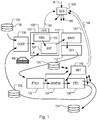
- Figure 1 at 100 shows a lithographic apparatus LA as part of an industrial facility implementing a high-volume, lithographic manufacturing process.
- the manufacturing process is adapted for the manufacture of for semiconductor products (integrated circuits) on substrates such as semiconductor wafers.
- semiconductor products integrated circuits
- substrates such as semiconductor wafers.
- semiconductor products integrated circuits
- the skilled person will appreciate that a wide variety of products can be manufactured by processing different types of substrates in variants of this process.
- the production of semiconductor products is used purely as an example which has great commercial significance today.
- a measurement station MEA is shown at 102 and an exposure station EXP is shown at 104.
- a control unit LACU is shown at 106.
- each substrate visits the measurement station and the exposure station to have a pattern applied.
- a projection system is used to transfer a product pattern from a patterning device MA onto the substrate using conditioned radiation and a projection system. This is done by forming an image of the pattern in a layer of radiation-sensitive resist material.
- the term "projection system” used herein should be broadly interpreted as encompassing any type of projection system, including refractive, reflective, catadioptric, magnetic, electromagnetic and electrostatic optical systems, or any combination thereof, as appropriate for the exposure radiation being used, or for other factors such as the use of an immersion liquid or the use of a vacuum.
- the patterning MA device may be a mask or reticle, which imparts a pattern to a radiation beam transmitted or reflected by the patterning device.
- Well-known modes of operation include a stepping mode and a scanning mode.
- the projection system may cooperate with support and positioning systems for the substrate and the patterning device in a variety of ways to apply a desired pattern to many target portions across a substrate.
- Programmable patterning devices may be used instead of reticles having a fixed pattern.
- the radiation for example may include electromagnetic radiation in the deep ultraviolet (DUV) or extreme ultraviolet (EUV) wavebands.
- DUV deep ultraviolet
- EUV extreme ultraviolet
- the present disclosure is also applicable to other types of lithographic process, for example imprint lithography and direct writing lithography, for example by electron beam.
- the lithographic apparatus control unit LACU controls all the movements and measurements of various actuators and sensors, causing the apparatus to receive substrates W and reticles MA and to implement the patterning operations.
- LACU also includes signal processing and computing capacity to implement desired calculations relevant to the operation of the apparatus.
- control unit LACU will be realized as a system of many sub-units, each handling the real-time data acquisition, processing and control of a subsystem or component within the apparatus.
- the substrate is processed in at the measurement station MEA so that various preparatory steps may be carried out.
- the preparatory steps may include mapping the surface height of the substrate using a level sensor and measuring the position of alignment marks on the substrate using an alignment sensor.
- the alignment marks are arranged nominally in a regular grid pattern. However, due to inaccuracies in creating the marks and also due to deformations of the substrate that occur throughout its processing, the marks deviate from the ideal grid. Consequently, in addition to measuring position and orientation of the substrate, the alignment sensor in practice must measure in detail the positions of many marks across the substrate area, if the apparatus is to print product features at the correct locations with very high accuracy.
- the lithographic apparatus LA may be of a so-called dual stage type which has two substrate tables, each with a positioning system controlled by the control unit LACU. While one substrate on one substrate table is being exposed at the exposure station EXP, another substrate can be loaded onto the other substrate table at the measurement station MEA so that various preparatory steps may be carried out.
- the measurement of alignment marks is therefore very time-consuming and the provision of two substrate tables enables a substantial increase in the throughput of the apparatus. If the position sensor IF is not capable of measuring the position of the substrate table while it is at the measurement station as well as at the exposure station, a second position sensor may be provided to enable the positions of the substrate table to be tracked at both stations.
- lithographic apparatus LA When lithographic apparatus LA is of a so-called dual stage type which has two substrate tables, the exposure station and the measurement station may be distinct locations between which the substrate tables can be exchanged. This is only one possible arrangement, however, and the measurement station and exposure station need not be so distinct. For example, it is known to have a single substrate table, to which a measurement stage is temporarily coupled during the pre-exposure measuring phase. The present disclosure is not limited to either type of system.
- apparatus 100 forms part of a "litho cell” or “litho cluster” that contains also a coating apparatus 108 for applying photosensitive resist and other coatings to substrates W for patterning by the apparatus 100.
- a baking apparatus 110 and developing apparatus 112 are provided for developing the exposed pattern into a physical resist pattern.
- substrate handling systems take care of supporting the substrates and transferring them from one piece of apparatus to the next.
- These apparatuses which are often collectively referred to as the "track" are under the control of a track control unit which is itself controlled by a supervisory control system SCS, which also controls the lithographic apparatus via lithographic apparatus control unit LACU.
- supervisory control system SCS receives recipe information R which provides in great detail a definition of the steps to be performed to create each patterned substrate.
- patterned substrates 120 are transferred to other processing apparatuses such as are illustrated at 122, 124, 126.
- apparatus 122 in this embodiment is an etching station, and apparatus 124 performs a post-etch annealing step. Further physical and/or chemical processing steps are applied in further apparatuses, 126, etc. Numerous types of operation can be required to make a real device, such as deposition of material, modification of surface material characteristics (oxidation, doping, ion implantation etc.), chemical-mechanical polishing (CMP), and so forth.
- the apparatus 126 may, in practice, represent a series of different processing steps performed in one or more apparatuses.
- substrates 130 arriving at the litho cluster may be newly prepared substrates, or they may be substrates that have been processed previously in this cluster or in another apparatus entirely.
- substrates 132 on leaving apparatus 126 may be returned for a subsequent patterning operation in the same litho cluster, they may be destined for patterning operations in a different cluster, or they may be finished products to be sent for dicing and packaging.
- Each layer of the product structure requires a different set of process steps, and the apparatuses 126 used at each layer may be completely different in type. Further, even where the processing steps to be applied by the apparatus 126 are nominally the same, in a large facility, there may be several supposedly identical machines working in parallel to perform the step 126 on different substrates. Small differences in set-up or faults between these machines can mean that they influence different substrates in different ways. Even steps that are relatively common to each layer, such as etching (apparatus 122) may be implemented by several etching apparatuses that are nominally identical but working in parallel to maximize throughput. In practice, moreover, different layers require different etch processes, for example chemical etches, plasma etches, according to the details of the material to be etched, and special requirements such as, for example, anisotropic etching.
- the previous and/or subsequent processes may be performed in other lithography apparatuses, as just mentioned, and may even be performed in different types of lithography apparatus.
- some layers in the device manufacturing process which are very demanding in parameters such as resolution and overlay may be performed in a more advanced lithography tool than other layers that are less demanding. Therefore some layers may be exposed in an immersion type lithography tool, while others are exposed in a 'dry' tool. Some layers may be exposed in a tool working at DUV wavelengths, while others are exposed using EUV wavelength radiation.
- a manufacturing facility in which litho cell LC is located also includes metrology system MET which receives some or all of the substrates W that have been processed in the litho cell. Metrology results are provided directly or indirectly to the supervisory control system (SCS) 138. If errors are detected, adjustments may be made to exposures of subsequent substrates, especially if the metrology can be done soon and fast enough that other substrates of the same batch are still to be exposed.
- SCS supervisory control system
- already exposed substrates may be stripped and reworked to improve yield, or discarded, thereby avoiding performing further processing on substrates that are known to be faulty. In a case where only some target portions of a substrate are faulty, further exposures can be performed only on those target portions which are good.
- a metrology apparatus 140 which is provided for making measurements of parameters of the products at desired stages in the manufacturing process.
- a common example of a metrology apparatus in a modern lithographic production facility is a scatterometer, for example an angle-resolved scatterometer or a spectroscopic scatterometer, and it may be applied to measure properties of the developed substrates at 120 prior to etching in the apparatus 122.
- a scatterometer for example an angle-resolved scatterometer or a spectroscopic scatterometer
- it may be applied to measure properties of the developed substrates at 120 prior to etching in the apparatus 122.
- it may be determined, for example, that important performance parameters such as overlay or critical dimension (CD) do not meet specified accuracy requirements in the developed resist.
- CD critical dimension
- the metrology results 142 from the apparatus 140 can be used to maintain accurate performance of the patterning operations in the litho cluster, by supervisory control system SCS and/or control unit LACU 106 making small adjustments 166 over time, thereby minimizing the risk of products being made out-of-specification, and requiring re-work.
- metrology apparatus 140 and/or other metrology apparatuses can be applied to measure properties of the processed substrates 132, 134, and incoming substrates 130.
- An embodiment of the present invention gives the ability to characterize the full stack of layers through the lifecycle of an integrated circuit, by using a lithographic apparatus with its built in sensors to capture fingerprints through the stack of layers. This characterization is correlated to the process steps in between exposures defining each layer.
- the analysis of fingerprints through the stack of layers provides the capability to correct for the phenomena in the multi-layer process which are complex and time varying. For example, new equipment and new process recipes are constantly generating new fingerprints.
- the lithographic apparatus has many in-line sensors in addition to alignment sensors. These include leveling sensors, sensors for aligning the reticle to the wafer stage chuck (e.g. "transmission image sensors” or “parallel integrated lens interferometer” type sensors) and sensors related to actuator stability.
- the lithographic apparatus' sensors are examples of sensors that can measure values of parameters spatially distributed across substrates. As well as a fingerprint representing the spatial distribution across the substrate, a fingerprint may represent a distribution of a process parameter across different wafers of a wafer lot. For example a fingerprint obtained from "parallel integrated lens interferometer” sensors could represent a reticle heating signature across the wafer lot.
- Embodiments of the present invention utilize these sensors to characterize many or all individual processes (for example etch, deposition, develop track). This is possible as the scanner is involved at least once during fabrication of a layer on a wafer. The scanner can apply its sensors to all wafers passing through the lithographic process at least once per layer.
- the scanner sensors used to determine a fingerprint may be dynamic. For example, for one layer the alignment sensor may be found to be most useful to determine a fingerprint representative for a process step, while for another layer a levelling sensor may be more informative.
- the use of sensors and the combination of sensor signals that yields most representative results may be subject to change and machine learning approaches may be used to converge to a per-layer optimal sensor signal constellation (e.g. layer 1: alignment color 1, layer 2: alignment color 2 + leveling, ... etc.)
- the lithographic apparatus can capture the fingerprints at all the different steps. Fingerprint patterns can be related to each other by performing a through-stack analysis and fingerprints common across layers can be related back to events and phenomena occurring at each layer. This makes possible to properly optimize the processing apparatuses for subsequent process steps. These subsequent process steps performed by the optimized apparatus may be applied to the wafers from which the fingerprints were obtained. In that case, the corrections are applied during the processing of a wafer through its stack of layers, as a kind of real-time correction. This is an example of optimizing an apparatus for processing product units from which the object data was measured, at subsequent stages in the multi-stage processing.
- the subsequent process steps performed by the optimized apparatus may apply to steps throughout the processing of other wafers, including wafers processed in future.
- the optimized apparatus may be used to perform process steps at earlier as well as later stages in the process flow than the stage at which the analysis and optimization is performed.
- the optimization can involve fixing an identified process apparatus and/or process recipe. It can also involve using dedicated scanner corrections via alignment or overlay corrections.
- Embodiments of the present invention provide dynamically refined (adaptive) computation of current relevant fingerprints in incoming measurement data, without hard assignment of fingerprints to process control threads.
- the fingerprints may be determined for various key performance indicators (e.g. available scanner data) and yield. Uncertainties are made explicit, and all data may be used for improved estimations of all fingerprints (not necessarily with a "hard” split per thread), while the factorial model leaves inference mechanism tractable.
- Embodiments of the present invention provide optimal initialization and in-line decomposition by combining fingerprints from domain knowledge and by decomposition of new incoming measurement data into the active fingerprint library.
- the underlying main fingerprints can be identified. Based on the decomposition actions can be identified for improvement.
- Embodiments of the present invention provide on-the-fly linking to context and yield impact assessment. Fingerprints may be linked to incoming context history in the fab, and used for real-time yield (electrical probing, voltage contrast, CD-SEM) impact assessment. Yield assessment may be performed during the IC manufacturing process, which is much earlier than when actual yield data available.
- Embodiments of the present invention provide a way to find and track the contributing factors, called active fingerprints (AFPs), to the wafer measurements in real-time.
- Wafer measurements include, but are not limited to, alignment, leveling, overlay and CD.
- embodiments incorporate the prior knowledge (i.e. domain expertise and mining of existing data) about common fingerprints, called reference fingerprints (RFPs), as well as real-time data analysis in order to find the main contributing factors in the wafer measurements. In other words, it finds the contributing factors by decomposing the wafer measurements to the current instantiation (AFPs) of the known fingerprints (RFPs).
- AFPs active fingerprints
- embodiments have a mechanism to track systematic changes and drifts (evolution) in the AFPs and find new fingerprints when the current set of AFPs is not enough for explaining the measurements.
- a validator may be integrated in the model that examines the newly found AFPs against statistical evidence coming from measurement to validate if the found AFP is systematic and not due to noise.
- Embodiments enable dynamic wafer control by exploiting the model for metrology estimation.
- Figure 2 is a flowchart of a method according to an embodiment of the present invention illustrating the reference fingerprint library and active fingerprint library.
- the active fingerprint library 216 is a set of fingerprints representing variation of one or more process parameters across one or more product units, such as wafers.
- New measurement data 204 of one or more parameters measured on one or more product unit is received.
- the active fingerprint library 216 is first updated based on an expected evolution of the set of fingerprints, which may be based on an expected evolution of one or more process parameters. Evolution herein means a gradual development. Further updating of the updated set of fingerprints is based on decomposition 206 of the received measurement data 204 in terms of the first updated set of fingerprints. If the decomposed fingerprints are similar 208 to the first updated fingerprints, then the active fingerprint library 216 may be updated by adapting 210 a fingerprint. If the fingerprints are not similar 208, then the active fingerprint library 216 may be updated by adding 212 a new fingerprint to the active library. Fingerprints may also be removed from the active library.
- Fingerprints may be added to the active library 216 by retrieving a fingerprint from a set of reference fingerprints in a reference fingerprint library 214. This can involve warping the retrieved fingerprint to determine the added fingerprint.
- the set of reference fingerprints in the reference fingerprint library 214 are derived from historical measurement data 202 representing one or more parameters measured on wafers.
- the reference fingerprint library 214 may be updated itself with an updated fingerprint from the active library 216.
- Examples 218 of fingerprints in the reference fingerprint library 214 are shown.
- the fingerprints are examples of writing errors 224, reticle heating 226, SUSD 230 (scan up/scan down effect, which is a measure of the shift of the fields exposed in the "up” scan direction with respect to the fields exposed in the "down” scan direction), etch 232, scanner chuck 238, CMP (chemical mechanical polish) 240, "ripple” 246 and anneal "dual swirl” 248.
- the initial fingerprints 220 of the active library 216 are shown. Fingerprints 234, 242 and 250 are copies of the reference fingerprints 232, 240 and 248 respectively. Fingerprints 222 at a later time in the active library 216 are also shown. Fingerprint 228 is an example of a new fingerprint added at step 212. Fingerprint 252 is an example of an adapted fingerprint from step 210. Fingerprints 236 and 244 are both still present, although their stored likelihoods of occurrence (not shown) may be different from one instance 220 to the other 222.
- Figure 3 is a flowchart of a method according to an embodiment of the present invention. It illustrates a method of maintaining a set of fingerprints in an active fingerprint library 316.
- the fingerprints represent variation of one or more process parameters across product units.
- the product units are wafer substrates.
- the method includes the steps: (a) receiving measurement data 324 of one or more parameters measured on wafers; (b) determining 320 a first updated set of fingerprints in the active fingerprint library 316 based on an expected evolution 322 of the set of fingerprints; and (c) determining 320 a second updated set of fingerprints based on decomposition of the received measurement data in terms of the first updated set of fingerprints.
- Each fingerprint may have a stored likelihood of occurrence, and the decomposition may involve: estimating, based the received measurement data, likelihoods of occurrence of the set of fingerprints in the received measurement data; and updating the stored likelihoods of occurrence based on the estimated likelihoods.
- the decomposition may comprises using a factorial model wherein the estimated likelihoods of occurrence comprise coefficients of the factorial model.
- Context data 324 represents records of one or more process parameters of the wafer(s) on which the measurement data was measured.
- the updating 320 of the active fingerprint library 316 may then be based on the context data 324.
- the step 320 of updating the active fingerprint library may comprise calculating 328 expected measurement data.
- the calculation is based on predicted 322 fingerprints, which themselves may be based on the expected evolution of the set of fingerprints.
- the expected evolution of the set of fingerprints may be based on a model predicting the evolution of the set of fingerprints based on knowledge associated with an observed evolution of one or more process parameters.
- the calculation is also based on the received context data.
- a process control action 326 is then determined based on the calculated expected measurement data.
- the fingerprints in the active fingerprint library 316 may then be updated based on the determined process control action 326.
- Updating 320 the set of fingerprints in the active library 316 may comprise adapting a fingerprint, adding a new fingerprint to the set and removing a fingerprint from the set.
- Fingerprints may be added to the active fingerprint library 316 by retrieving (fetching) 312 a fingerprint from a set of reference fingerprints in a reference fingerprint library 310. This may involve warping 312 the retrieved fingerprint to determine the added fingerprint.
- the set of reference fingerprints in the reference fingerprint library 310 are derived 308 from historical measurement data 304 representing one or more parameters measured on wafers.
- the reference fingerprint library 310 can be updated 314 with an updated fingerprint from the active fingerprint library 316.
- User input 318 may be used to validate 314 the update.
- Initial Setup 302-308 During initial setup reference fingerprints may be identified using three procedures:
- the method's process flow contains three intertwined loops: identification, updating and control.
- the identification loop (shown within 310, 312, 316, 314) is asynchronous governed by the rate of insertion of dynamically identified fingerprints in the reference library.
- the updating (within 316, 322, 320) and control loop (within 322, 328, 326) cycles are synchronized to the rate of receiving wafer measurements (per wafer).
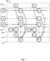
- Figure 4 illustrates the dynamic model of the active fingerprint library.
- x t j is the state of the active fingerprint at the time of observation t-th wafer measurement z t 412.
- u t is the control action 402 and
- c t is the context information used in context sensitive clustering 408.
- a t is the decomposition coefficient 410.
- FIG 5 illustrates a simplified example of the dynamic model of Figure 4 .
- two fingerprints 506 and 508 are in the reference fingerprint library (referred to as 'scaling' and 'dual swirl' fingerprints respectively). They are also shown as reference fingerprints R1 and R2. Their evolution in the active library at two time instances 502 and 504 are shown.
- the patterns 510 and 512 are shown at time 502 and the corresponding active fingerprints are also represented as A1 and A2.
- the patterns 514 and 516 are shown at time 504 and the corresponding active fingerprints are again represented as A1 and A2.
- Measurements are leveling LV, alignment AL and overlay OV. Note that some measurements are not always available (e.g. OV) but when they are provided they may be utilized. Fingerprints in the library represent a common cause for the patterns seen in the wafer measurements and they manifest themselves in different type of measurements. The contribution of fingerprints A1 and A2 in the measurements AL, LV and OV depends on the context of processing CO and metrology.
- the measurement result 518 of alignment measurement AL and the measurement result 520 of leveling measurement LV are shown.
- the measurement result 522 of alignment measurement AL, the measurement result 524 of leveling measurement LV, and the measurement result 526 of overlay measurement OV are shown. Horizontal arrows show evolution of fingerprints A1 and A2.
- Evolution herein may be temporal (for example when measurements are on single layer of different chronologically ordered wafers) or thru-stack (for example when measurement are on multiple chronologically ordered layers of one wafer).
- dual swirl fingerprint 508 slightly rotates between two time instances 502 and 504, as seen by comparing 512 and 516.
- An embodiment of the invention may be implemented using a computer program containing one or more sequences of machine-readable instructions describing methods of maintaining a set of fingerprints, as described above.
- This computer program may be executed within a computing apparatus, such as control unit LACU of Figure 1 , or some other controller.
- a data storage medium e.g., semiconductor memory, magnetic or optical disk having such a computer program stored therein.
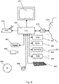
- This control unit LACU may include a computer assembly as shown in Figure 6 .
- the computer assembly may be a dedicated computer in the form of a control unit in embodiments of the assembly according to the invention or, alternatively, be a central computer controlling the lithographic apparatus.
- the computer assembly may be arranged for loading a computer program product comprising computer executable code. This may enable the computer assembly, when the computer program product is downloaded, to control aforementioned uses of a lithographic apparatus with embodiments of the level and alignment sensors AS, LS.
- Memory 829 connected to processor 827 may comprise a number of memory components like a hard disk 861, Read Only Memory (ROM) 862, Electrically Erasable Programmable Read Only Memory (EEPROM) 863 and Random Access Memory (RAM) 864. Not all aforementioned memory components need to be present. Furthermore, it is not essential that aforementioned memory components are physically in close proximity to the processor 827 or to each other. They may be located at a distance away.
- ROM Read Only Memory
- EEPROM Electrically Erasable Programmable Read Only Memory
- RAM Random Access Memory
- the processor 827 may also be connected to some kind of user interface, for instance a keyboard 865 or a mouse 866.
- a keyboard 865 or a mouse 866 may also be connected to some kind of user interface.
- a touch screen, track ball, speech converter or other interfaces that are known to persons skilled in the art may also be used.
- the processor 827 may be connected to a reading unit 867, which is arranged to read data, e.g. in the form of computer executable code, from and under some circumstances store data on a data carrier, like a solid-state drive 868 or a CDROM 869. Also DVD's or other data carriers known to persons skilled in the art may be used.
- a reading unit 867 which is arranged to read data, e.g. in the form of computer executable code, from and under some circumstances store data on a data carrier, like a solid-state drive 868 or a CDROM 869. Also DVD's or other data carriers known to persons skilled in the art may be used.
- the processor 827 may also be connected to a printer 870 to print out output data on paper as well as to a display 871, for instance a monitor or LCD (Liquid Crystal Display), of any other type of display known to a person skilled in the art.
- a printer 870 to print out output data on paper as well as to a display 871, for instance a monitor or LCD (Liquid Crystal Display), of any other type of display known to a person skilled in the art.
- LCD Liquid Crystal Display
- the processor 827 may be connected to a communications network 872, for instance a public switched telephone network (PSTN), a local area network (LAN), a wide area network (WAN) etc. by means of transmitters/receivers 873 responsible for input/output (I/O).
- the processor 827 may be arranged to communicate with other communication systems via the communications network 872.
- external computers not shown, for instance personal computers of operators, can log into the processor 827 via the communications network 872.
- the processor 827 may be implemented as an independent system or as a number of processing units that operate in parallel, wherein each processing unit is arranged to execute subtasks of a larger program.
- the processing units may also be divided in one or more main processing units with several sub-processing units. Some processing units of the processor 827 may even be located a distance away of the other processing units and communicate via communications network 872. Connections between modules can be made wired or wireless.
- the computer system can be any signal processing system with analogue and/or digital and/or software technology arranged to perform the functions discussed here.
Landscapes
- Physics & Mathematics (AREA)
- General Physics & Mathematics (AREA)
- Engineering & Computer Science (AREA)
- Health & Medical Sciences (AREA)
- Artificial Intelligence (AREA)
- Computer Vision & Pattern Recognition (AREA)
- Evolutionary Computation (AREA)
- Medical Informatics (AREA)
- Software Systems (AREA)
- Data Mining & Analysis (AREA)
- Exposure And Positioning Against Photoresist Photosensitive Materials (AREA)
- Testing Or Measuring Of Semiconductors Or The Like (AREA)
Abstract
A method of maintaining a set of fingerprints (316) representing variation of one or more process parameters across wafers, has the steps: (a) receiving measurement data (324) of one or more parameters measured on wafers; (b) updating (320) the set of fingerprints based on an expected evolution (322) of the one or more process parameters; and (c) evaluation of the updated set of fingerprints based on decomposition of the received measurement data in terms of the updated set of fingerprints. Each fingerprint may have a stored likelihood of occurrence (316), and the decomposition may involve: estimating, based the received measurement data (324), likelihoods of occurrence of the set of fingerprints in the received measurement data; and updating the stored likelihoods of occurrence based on the estimated likelihoods.
Description
- The present invention relates to a method of maintaining a set of fingerprints representing variation of one or more process parameters associated with one or more product units, usable, for example, in the manufacture of devices by lithographic techniques. The present invention also relates to associated computer programs and computer program products, and apparatus.
- A lithographic apparatus is a machine that applies a desired pattern onto a substrate, usually onto a target portion of the substrate. A lithographic apparatus can be used, for example, in the manufacture of integrated circuits (ICs). In that instance, a patterning device, which is alternatively referred to as a mask or a reticle, may be used to generate a circuit pattern to be formed on an individual layer of the IC. This pattern can be transferred onto a target portion (e.g., including part of, one, or several dies) on a substrate (e.g., a silicon wafer). Transfer of the pattern is typically via imaging onto a layer of radiation-sensitive material (resist) provided on the substrate. In general, a single substrate will contain a network of adjacent target portions that are successively patterned. These target portions are commonly referred to as "fields". Wafers are processed in batches or lots through various apparatuses in the semiconductor fabrication facility (fab). The integrated circuit is built up layer by layer with a lithographic step performed by a lithographic apparatus at each layer and other fab processes being performed in between lithographic steps.
- Before the imaging step, various chemical and/or physical processing steps are used to form and prepare the layer for patterning. After the imaging step defines the pattern, further chemical and/or physical processing steps work through the pattern to create functional features of the integrated circuit. The imaging and processing steps are repeated in a multi-layer process to build integrated circuit.
- The accurate placement of patterns on the substrate is a chief challenge for reducing the size of circuit components and other products that may be produced by lithography. In particular, the challenge of measuring accurately the features on a substrate which have already been laid down is a critical step in being able to align successive layers of features in superposition accurately enough to produce working devices with a high yield. So-called overlay should, in general, be achieved within a few tens of nanometers in today's sub-micron semiconductor devices, down to a few nanometers in the most critical layers.
- Consequently, modern lithography apparatuses involve extensive measurement or 'mapping' operations prior to the step of actually exposing or otherwise patterning the substrate at a target location. So-called advanced alignment models have been and continue to be developed to model and correct more accurately non-linear distortions of the wafer 'grid' that are caused by processing steps and/or by the lithographic apparatus itself. Not all distortions are correctable during exposure, however, and it remains important to trace and eliminate as many causes of such distortions as possible.
- Modern multi-layer lithographic processes and products are so complex that issues due to processing are difficult to trace back to the root cause. Monitoring of wafer integrity and design of an appropriate correction strategy is therefore a time-consuming and laborious exercise.
- International Patent Application
WO 2015049087 , which is incorporated by reference herein in its entirety, discloses a method of obtaining diagnostic information relating to an industrial process. Alignment data or other measurements are made at stages during the performance of the lithographic process to obtain object data representing positional deviation or other parameters measured at points spatially distributed across each wafer. Overlay and alignment residuals typically show patterns across the wafer, known as fingerprints. This object data is used to obtain diagnostic information by performing a multivariate analysis to decompose the set of vectors representing the wafers in multidimensional space into one or more component vectors. Diagnostic information about the industrial process is extracted using the component vectors. The performance of the industrial process for subsequent wafers can be controlled based on the extracted diagnostic information. - In the fab, semiconductor process steps may thus leave their fingerprints on the product wafers. The lithographic apparatus has many in-line sensors, in addition to alignment sensors, that can measure these fingerprints. These include leveling sensors, sensors for aligning the reticle to the wafer stage chuck (e.g. "transmission image sensors" or "parallel integrated lens interferometer" type sensors) and sensors related to actuator stability. The lithographic apparatus' sensors are examples of sensors that can measure values of parameters spatially distributed across substrates. As well as a fingerprint representing the spatial distribution across the substrate, a fingerprint may represent a distribution of a process parameter across different wafers of a wafer lot. The term "process parameter" in this document needs to be read as any parameter associated with the semiconductor manufacturing process that may be relevant for a fingerprint of a (process) parameter fingerprint on a product unit (e.g. a substrate, wafer). A process parameter may hence be a parameter associated with a measurement performed by a sensor (for example within the lithographic apparatus or an etching apparatus) or (context) information related to a configuration of one or more of the apparatus used within the semiconductor manufacturing process (e.g. a certain etch chamber used for etching). For example a fingerprint obtained from "parallel integrated lens interferometer" sensors could represent a reticle heating signature across the wafer lot. Embodiments of the present invention utilize these sensors to characterize many or all individual processes (e.g. etch, deposition, develop track). This is possible as the scanner is involved at least once during fabrication of a layer on a wafer. The scanner can apply its sensors to all wafers passing through the lithographic process at least once per layer.
- Via the many sensors, wafer, zone, field and die fingerprints may be derived from the wafers that are being exposed. It is useful to identify the fingerprints that are present on a certain set of layers on a wafer, and relate the presence of these fingerprints to processing and scanner context (to find the 'root cause') and expected on-product performance effects such as overlay, CD (critical dimension), focus, voltage contrast, CD-SEM, electrical tests (to determine 'yield impact').
- Fingerprints referred to herein are the main systematic contributors (or "latent factors") of the measured signal. They are typically connected to the performance impact on-wafer or to previous processing steps. They can refer to wafer grid patterns (e.g. from alignment, leveling, overlay, focus, CD), field patterns (e.g. from intrafield alignment, leveling, overlay, focus, CD), wafer zone patterns (e.g. outermost radius of wafer measurements) or even patterns in scanner measurements related to wafer exposure (e.g. heating signature through-lot from reticle align "transmission image sensors" or "parallel integrated lens interferometer" type sensors measurements, temperature / pressure / servo profiles, etc.).
- Measurement data referred to herein may be any measurements performed on the wafer and intended to be used for monitoring and control, e.g. leveling, alignment, overlay, CD, focus, SWA (side-wall angle), etc.
- A fingerprint library referred to herein is a collection or set of fingerprints that may be encoded homogenously or heterogeneously.
- Conventional control strategies try to minimize the average observed error (e.g. overlay, focus, CD) in a lot or group of wafers. There are two limitations with this approach: the control/monitoring is done with hard assignment by assuming clustering among wafers; the fact that the monitored feature (overlay, CD, etc.) is the contribution of the different factors is ignored in these methods. This is particularly restrictive when the scope of the monitoring/control is extended, space-wise, from scanner to the whole-fab and, time-wise, from per-layer to through-stack.
- In particular, one would like to understand the main fingerprints that contribute to potential overlay/CD/focus issues and eventually yield issues - when retrieving data from exposures of a new product/node/process in the ramp up phase in a semiconductor fab. Fine tuning and troubleshooting using convention methods may take months of time from an experienced semiconductor engineer, which is compromising time-to-yield - and hence time-to-market of a new product/node/process.
- The inventors have devised a way to maintain a set of fingerprints while avoiding or at least mitigating one or more of the associated problems mentioned above.
- The invention in a first aspect provides a method of maintaining a set of fingerprints representing variation of one or more process parameters associated with one or more product units, the method comprising the steps:
- (a) receiving measurement data of one or more parameters measured on one or more product units;
- (b) determining a first updated set of fingerprints based on an expected evolution of the set of fingerprints; and
- (c) determining a second updated set of fingerprints based on decomposition of the received measurement data in terms of the first updated set of fingerprints.
- The invention in a second aspect provides a computer program comprising computer readable instructions which, when run on suitable computer apparatus, cause the computer apparatus to perform the method of the first aspect.
- The invention in a third aspect provides a computer program product comprising the computer program of the second aspect.
- The invention in a fourth aspect provides an apparatus specifically adapted to carry out the steps of the method of the first aspect.
- Embodiments of the invention will now be described, by way of example, with reference to the accompanying drawings in which:
-
Figure 1 depicts a lithographic apparatus together with other apparatuses forming a production facility for semiconductor devices. -
Figure 2 is a flowchart of a method according to an embodiment of the present invention illustrating the reference fingerprint library and active fingerprint library. -
Figure 3 is a flowchart of a method according to an embodiment of the present invention. -
Figure 4 illustrates the dynamic model of the active fingerprint library. -
Figure 5 illustrates a simplified example of the dynamic model ofFigure 4 . -
Figure 6 illustrates computing apparatus hardware useful in implementing the methods disclosed herein. - Before describing embodiments of the invention in detail, it is instructive to present an example environment in which embodiments of the present invention may be implemented.
-
Figure 1 at 100 shows a lithographic apparatus LA as part of an industrial facility implementing a high-volume, lithographic manufacturing process. In the present example, the manufacturing process is adapted for the manufacture of for semiconductor products (integrated circuits) on substrates such as semiconductor wafers. The skilled person will appreciate that a wide variety of products can be manufactured by processing different types of substrates in variants of this process. The production of semiconductor products is used purely as an example which has great commercial significance today. - Within the lithographic apparatus (or "litho tool" 100 for short), a measurement station MEA is shown at 102 and an exposure station EXP is shown at 104. A control unit LACU is shown at 106. In this example, each substrate visits the measurement station and the exposure station to have a pattern applied. In an optical lithographic apparatus, for example, a projection system is used to transfer a product pattern from a patterning device MA onto the substrate using conditioned radiation and a projection system. This is done by forming an image of the pattern in a layer of radiation-sensitive resist material.
- The term "projection system" used herein should be broadly interpreted as encompassing any type of projection system, including refractive, reflective, catadioptric, magnetic, electromagnetic and electrostatic optical systems, or any combination thereof, as appropriate for the exposure radiation being used, or for other factors such as the use of an immersion liquid or the use of a vacuum. The patterning MA device may be a mask or reticle, which imparts a pattern to a radiation beam transmitted or reflected by the patterning device. Well-known modes of operation include a stepping mode and a scanning mode. As is well known, the projection system may cooperate with support and positioning systems for the substrate and the patterning device in a variety of ways to apply a desired pattern to many target portions across a substrate. Programmable patterning devices may be used instead of reticles having a fixed pattern. The radiation for example may include electromagnetic radiation in the deep ultraviolet (DUV) or extreme ultraviolet (EUV) wavebands. The present disclosure is also applicable to other types of lithographic process, for example imprint lithography and direct writing lithography, for example by electron beam.
- The lithographic apparatus control unit LACU controls all the movements and measurements of various actuators and sensors, causing the apparatus to receive substrates W and reticles MA and to implement the patterning operations. LACU also includes signal processing and computing capacity to implement desired calculations relevant to the operation of the apparatus. In practice, control unit LACU will be realized as a system of many sub-units, each handling the real-time data acquisition, processing and control of a subsystem or component within the apparatus.
- Before the pattern is applied to a substrate at the exposure station EXP, the substrate is processed in at the measurement station MEA so that various preparatory steps may be carried out. The preparatory steps may include mapping the surface height of the substrate using a level sensor and measuring the position of alignment marks on the substrate using an alignment sensor. The alignment marks are arranged nominally in a regular grid pattern. However, due to inaccuracies in creating the marks and also due to deformations of the substrate that occur throughout its processing, the marks deviate from the ideal grid. Consequently, in addition to measuring position and orientation of the substrate, the alignment sensor in practice must measure in detail the positions of many marks across the substrate area, if the apparatus is to print product features at the correct locations with very high accuracy.
- The lithographic apparatus LA may be of a so-called dual stage type which has two substrate tables, each with a positioning system controlled by the control unit LACU. While one substrate on one substrate table is being exposed at the exposure station EXP, another substrate can be loaded onto the other substrate table at the measurement station MEA so that various preparatory steps may be carried out. The measurement of alignment marks is therefore very time-consuming and the provision of two substrate tables enables a substantial increase in the throughput of the apparatus. If the position sensor IF is not capable of measuring the position of the substrate table while it is at the measurement station as well as at the exposure station, a second position sensor may be provided to enable the positions of the substrate table to be tracked at both stations. When lithographic apparatus LA is of a so-called dual stage type which has two substrate tables, the exposure station and the measurement station may be distinct locations between which the substrate tables can be exchanged. This is only one possible arrangement, however, and the measurement station and exposure station need not be so distinct. For example, it is known to have a single substrate table, to which a measurement stage is temporarily coupled during the pre-exposure measuring phase. The present disclosure is not limited to either type of system.
- Within the production facility,
apparatus 100 forms part of a "litho cell" or "litho cluster" that contains also acoating apparatus 108 for applying photosensitive resist and other coatings to substrates W for patterning by theapparatus 100. At an output side ofapparatus 100, abaking apparatus 110 and developingapparatus 112 are provided for developing the exposed pattern into a physical resist pattern. Between all of these apparatuses, substrate handling systems take care of supporting the substrates and transferring them from one piece of apparatus to the next. These apparatuses, which are often collectively referred to as the "track", are under the control of a track control unit which is itself controlled by a supervisory control system SCS, which also controls the lithographic apparatus via lithographic apparatus control unit LACU. Thus, the different apparatuses can be operated to maximize throughput and processing efficiency. Supervisory control system SCS receives recipe information R which provides in great detail a definition of the steps to be performed to create each patterned substrate. - Once the pattern has been applied and developed in the litho cell, patterned
substrates 120 are transferred to other processing apparatuses such as are illustrated at 122, 124, 126. A wide range of processing steps is implemented by various apparatuses in a typical manufacturing facility. For the sake of example,apparatus 122 in this embodiment is an etching station, andapparatus 124 performs a post-etch annealing step. Further physical and/or chemical processing steps are applied in further apparatuses, 126, etc. Numerous types of operation can be required to make a real device, such as deposition of material, modification of surface material characteristics (oxidation, doping, ion implantation etc.), chemical-mechanical polishing (CMP), and so forth. Theapparatus 126 may, in practice, represent a series of different processing steps performed in one or more apparatuses. - As is well known, the manufacture of semiconductor devices involves many repetitions of such processing, to build up device structures with appropriate materials and patterns, layer-by-layer on the substrate. Accordingly,
substrates 130 arriving at the litho cluster may be newly prepared substrates, or they may be substrates that have been processed previously in this cluster or in another apparatus entirely. Similarly, depending on the required processing,substrates 132 on leavingapparatus 126 may be returned for a subsequent patterning operation in the same litho cluster, they may be destined for patterning operations in a different cluster, or they may be finished products to be sent for dicing and packaging. - Each layer of the product structure requires a different set of process steps, and the
apparatuses 126 used at each layer may be completely different in type. Further, even where the processing steps to be applied by theapparatus 126 are nominally the same, in a large facility, there may be several supposedly identical machines working in parallel to perform thestep 126 on different substrates. Small differences in set-up or faults between these machines can mean that they influence different substrates in different ways. Even steps that are relatively common to each layer, such as etching (apparatus 122) may be implemented by several etching apparatuses that are nominally identical but working in parallel to maximize throughput. In practice, moreover, different layers require different etch processes, for example chemical etches, plasma etches, according to the details of the material to be etched, and special requirements such as, for example, anisotropic etching. - The previous and/or subsequent processes may be performed in other lithography apparatuses, as just mentioned, and may even be performed in different types of lithography apparatus. For example, some layers in the device manufacturing process which are very demanding in parameters such as resolution and overlay may be performed in a more advanced lithography tool than other layers that are less demanding. Therefore some layers may be exposed in an immersion type lithography tool, while others are exposed in a 'dry' tool. Some layers may be exposed in a tool working at DUV wavelengths, while others are exposed using EUV wavelength radiation.
- In order that the substrates that are exposed by the lithographic apparatus are exposed correctly and consistently, it is desirable to inspect exposed substrates to measure properties such as overlay errors between subsequent layers, line thicknesses, critical dimensions (CD), etc. Accordingly a manufacturing facility in which litho cell LC is located also includes metrology system MET which receives some or all of the substrates W that have been processed in the litho cell. Metrology results are provided directly or indirectly to the supervisory control system (SCS) 138. If errors are detected, adjustments may be made to exposures of subsequent substrates, especially if the metrology can be done soon and fast enough that other substrates of the same batch are still to be exposed. Also, already exposed substrates may be stripped and reworked to improve yield, or discarded, thereby avoiding performing further processing on substrates that are known to be faulty. In a case where only some target portions of a substrate are faulty, further exposures can be performed only on those target portions which are good.
- Also shown in
Figure 1 is ametrology apparatus 140 which is provided for making measurements of parameters of the products at desired stages in the manufacturing process. A common example of a metrology apparatus in a modern lithographic production facility is a scatterometer, for example an angle-resolved scatterometer or a spectroscopic scatterometer, and it may be applied to measure properties of the developed substrates at 120 prior to etching in theapparatus 122. Usingmetrology apparatus 140, it may be determined, for example, that important performance parameters such as overlay or critical dimension (CD) do not meet specified accuracy requirements in the developed resist. Prior to the etching step, the opportunity exists to strip the developed resist and reprocess thesubstrates 120 through the litho cluster. As is also well known, the metrology results 142 from theapparatus 140 can be used to maintain accurate performance of the patterning operations in the litho cluster, by supervisory control system SCS and/orcontrol unit LACU 106 makingsmall adjustments 166 over time, thereby minimizing the risk of products being made out-of-specification, and requiring re-work. Of course,metrology apparatus 140 and/or other metrology apparatuses (not shown) can be applied to measure properties of the processedsubstrates incoming substrates 130. - An embodiment of the present invention gives the ability to characterize the full stack of layers through the lifecycle of an integrated circuit, by using a lithographic apparatus with its built in sensors to capture fingerprints through the stack of layers. This characterization is correlated to the process steps in between exposures defining each layer. The analysis of fingerprints through the stack of layers provides the capability to correct for the phenomena in the multi-layer process which are complex and time varying. For example, new equipment and new process recipes are constantly generating new fingerprints.
- The lithographic apparatus has many in-line sensors in addition to alignment sensors. These include leveling sensors, sensors for aligning the reticle to the wafer stage chuck (e.g. "transmission image sensors" or "parallel integrated lens interferometer" type sensors) and sensors related to actuator stability. The lithographic apparatus' sensors are examples of sensors that can measure values of parameters spatially distributed across substrates. As well as a fingerprint representing the spatial distribution across the substrate, a fingerprint may represent a distribution of a process parameter across different wafers of a wafer lot. For example a fingerprint obtained from "parallel integrated lens interferometer" sensors could represent a reticle heating signature across the wafer lot. Embodiments of the present invention utilize these sensors to characterize many or all individual processes (for example etch, deposition, develop track). This is possible as the scanner is involved at least once during fabrication of a layer on a wafer. The scanner can apply its sensors to all wafers passing through the lithographic process at least once per layer.
- The scanner sensors used to determine a fingerprint may be dynamic. For example, for one layer the alignment sensor may be found to be most useful to determine a fingerprint representative for a process step, while for another layer a levelling sensor may be more informative. The use of sensors and the combination of sensor signals that yields most representative results (e.g. most informative for process control and processing apparatus optimization) may be subject to change and machine learning approaches may be used to converge to a per-layer optimal sensor signal constellation (e.g. layer 1:
alignment color 1, layer 2:alignment color 2 + leveling, ... etc.) - As mentioned above, the wafers are processed through the stack of layers, the lithographic apparatus can capture the fingerprints at all the different steps. Fingerprint patterns can be related to each other by performing a through-stack analysis and fingerprints common across layers can be related back to events and phenomena occurring at each layer. This makes possible to properly optimize the processing apparatuses for subsequent process steps. These subsequent process steps performed by the optimized apparatus may be applied to the wafers from which the fingerprints were obtained. In that case, the corrections are applied during the processing of a wafer through its stack of layers, as a kind of real-time correction. This is an example of optimizing an apparatus for processing product units from which the object data was measured, at subsequent stages in the multi-stage processing. The subsequent process steps performed by the optimized apparatus may apply to steps throughout the processing of other wafers, including wafers processed in future. The optimized apparatus may be used to perform process steps at earlier as well as later stages in the process flow than the stage at which the analysis and optimization is performed. The optimization can involve fixing an identified process apparatus and/or process recipe. It can also involve using dedicated scanner corrections via alignment or overlay corrections.
- Embodiments of the present invention provide dynamically refined (adaptive) computation of current relevant fingerprints in incoming measurement data, without hard assignment of fingerprints to process control threads. The fingerprints may be determined for various key performance indicators (e.g. available scanner data) and yield. Uncertainties are made explicit, and all data may be used for improved estimations of all fingerprints (not necessarily with a "hard" split per thread), while the factorial model leaves inference mechanism tractable.
- Embodiments of the present invention provide optimal initialization and in-line decomposition by combining fingerprints from domain knowledge and by decomposition of new incoming measurement data into the active fingerprint library.
- After decomposition of the received measurement data, the underlying main fingerprints can be identified. Based on the decomposition actions can be identified for improvement.
- Embodiments of the present invention provide on-the-fly linking to context and yield impact assessment. Fingerprints may be linked to incoming context history in the fab, and used for real-time yield (electrical probing, voltage contrast, CD-SEM) impact assessment. Yield assessment may be performed during the IC manufacturing process, which is much earlier than when actual yield data available.
- Embodiments of the present invention provide a way to find and track the contributing factors, called active fingerprints (AFPs), to the wafer measurements in real-time. Wafer measurements include, but are not limited to, alignment, leveling, overlay and CD. In order to achieve this, embodiments incorporate the prior knowledge (i.e. domain expertise and mining of existing data) about common fingerprints, called reference fingerprints (RFPs), as well as real-time data analysis in order to find the main contributing factors in the wafer measurements. In other words, it finds the contributing factors by decomposing the wafer measurements to the current instantiation (AFPs) of the known fingerprints (RFPs). Furthermore, embodiments have a mechanism to track systematic changes and drifts (evolution) in the AFPs and find new fingerprints when the current set of AFPs is not enough for explaining the measurements. In addition, a validator may be integrated in the model that examines the newly found AFPs against statistical evidence coming from measurement to validate if the found AFP is systematic and not due to noise. Embodiments enable dynamic wafer control by exploiting the model for metrology estimation.
- Hence we are able to monitor the contribution of different factors in the measurements as well as keeping track of the fingerprints they put on the wafer. This results in a more natural fab process model that enables adaptive and dynamic control mechanism for per-wafer optimal control estimation and on-product performance impact analysis. In addition, this method can facilitate the root-cause and performance impact analysis as the factors can be traced through-stack and linked to process steps.
-
Figure 2 is a flowchart of a method according to an embodiment of the present invention illustrating the reference fingerprint library and active fingerprint library. - With reference to
Figure 2 , theactive fingerprint library 216 is a set of fingerprints representing variation of one or more process parameters across one or more product units, such as wafers.New measurement data 204 of one or more parameters measured on one or more product unit is received. Theactive fingerprint library 216 is first updated based on an expected evolution of the set of fingerprints, which may be based on an expected evolution of one or more process parameters. Evolution herein means a gradual development. Further updating of the updated set of fingerprints is based ondecomposition 206 of the receivedmeasurement data 204 in terms of the first updated set of fingerprints. If the decomposed fingerprints are similar 208 to the first updated fingerprints, then theactive fingerprint library 216 may be updated by adapting 210 a fingerprint. If the fingerprints are not similar 208, then theactive fingerprint library 216 may be updated by adding 212 a new fingerprint to the active library. Fingerprints may also be removed from the active library. - Fingerprints may be added to the
active library 216 by retrieving a fingerprint from a set of reference fingerprints in areference fingerprint library 214. This can involve warping the retrieved fingerprint to determine the added fingerprint. The set of reference fingerprints in thereference fingerprint library 214 are derived fromhistorical measurement data 202 representing one or more parameters measured on wafers. - The
reference fingerprint library 214 may be updated itself with an updated fingerprint from theactive library 216. - Examples 218 of fingerprints in the
reference fingerprint library 214 are shown. The fingerprints are examples of writing errors 224,reticle heating 226, SUSD 230 (scan up/scan down effect, which is a measure of the shift of the fields exposed in the "up" scan direction with respect to the fields exposed in the "down" scan direction),etch 232, scanner chuck 238, CMP (chemical mechanical polish) 240, "ripple" 246 and anneal "dual swirl" 248. - The
initial fingerprints 220 of theactive library 216 are shown.Fingerprints reference fingerprints Fingerprints 222 at a later time in theactive library 216 are also shown.Fingerprint 228 is an example of a new fingerprint added atstep 212.Fingerprint 252 is an example of an adapted fingerprint fromstep 210.Fingerprints 236 and 244 are both still present, although their stored likelihoods of occurrence (not shown) may be different from oneinstance 220 to the other 222. -
Figure 3 is a flowchart of a method according to an embodiment of the present invention. It illustrates a method of maintaining a set of fingerprints in anactive fingerprint library 316. The fingerprints represent variation of one or more process parameters across product units. In this example, the product units are wafer substrates. The method includes the steps: (a) receivingmeasurement data 324 of one or more parameters measured on wafers; (b) determining 320 a first updated set of fingerprints in theactive fingerprint library 316 based on an expectedevolution 322 of the set of fingerprints; and (c) determining 320 a second updated set of fingerprints based on decomposition of the received measurement data in terms of the first updated set of fingerprints. Each fingerprint may have a stored likelihood of occurrence, and the decomposition may involve: estimating, based the received measurement data, likelihoods of occurrence of the set of fingerprints in the received measurement data; and updating the stored likelihoods of occurrence based on the estimated likelihoods. - The decomposition may comprises using a factorial model wherein the estimated likelihoods of occurrence comprise coefficients of the factorial model.
-
Context data 324 represents records of one or more process parameters of the wafer(s) on which the measurement data was measured. The updating 320 of theactive fingerprint library 316 may then be based on thecontext data 324. - The
step 320 of updating the active fingerprint library may comprise calculating 328 expected measurement data. The calculation is based on predicted 322 fingerprints, which themselves may be based on the expected evolution of the set of fingerprints. The expected evolution of the set of fingerprints may be based on a model predicting the evolution of the set of fingerprints based on knowledge associated with an observed evolution of one or more process parameters. The calculation is also based on the received context data. Aprocess control action 326 is then determined based on the calculated expected measurement data. The fingerprints in theactive fingerprint library 316 may then be updated based on the determinedprocess control action 326. - Updating 320 the set of fingerprints in the
active library 316 may comprise adapting a fingerprint, adding a new fingerprint to the set and removing a fingerprint from the set. - Fingerprints may be added to the
active fingerprint library 316 by retrieving (fetching) 312 a fingerprint from a set of reference fingerprints in areference fingerprint library 310. This may involve warping 312 the retrieved fingerprint to determine the added fingerprint. - The set of reference fingerprints in the
reference fingerprint library 310 are derived 308 fromhistorical measurement data 304 representing one or more parameters measured on wafers. - The
reference fingerprint library 310 can be updated 314 with an updated fingerprint from theactive fingerprint library 316.User input 318 may be used to validate 314 the update. - These steps are described in more detail below.
- Initial Setup 302-308: During initial setup reference fingerprints may be identified using three procedures:
- Knowledge elicitation 306: Domain experts are consulted 302 for identification of fingerprints tool/process fingerprints they recognize. The fingerprints' shapes and variations are then encoded in the parametric or non-parametric form and put in the
reference fingerprint library 310. - Data mining 308:
Historical measurement data 304 is analyzed 308 by means of different exploratory data analysis techniques, e.g. cluster analysis, component analysis, to identify fingerprints. The fingerprints shapes and variations are then encoded in the parametric or non-parametric form and put in the reference fingerprint library. - Dynamic identification 314: Factors recognized by the adaptation procedure during wafer measurement decomposition are described below.
- Reference Library 310-312: Consists of a repository of generic and heterogeneous fingerprints and some functionality to instantiate the fingerprints on a desired layout.
- Reference Fingerprints 310: Container where generic fingerprints objects, called reference fingerprints, known from historical observations or physical definition, are stored. The fingerprints may be encoded in different parametric and non-parametric ways. The information of each fingerprint may contain its average shape, the shape variation and meta-data information about its history, root-causes, etc.
- Fetch & Warp 312: The process of instantiating a generic reference fingerprint on the desired layout. This may generate a form of probability distribution that represents the shape of the fingerprint and its variation. This may be done by statistical function regression techniques (such as Gaussian Process, linear regression etc.) and/or by sampling techniques (Monte-Carlo sampling) and/or by parametric function evaluation. Warping means: not only layout-adaptations but also shape adaptations can be applied to instantiate the generic reference fingerprint. E.g. affine transformations of a basic shape (translating, rotating, scaling the shape) may be considered 'admissible variants' of the same shape. Warping may be implemented explicitly (e.g. by executing the transformation when instantiating), or implicitly (e.g. by using a rotation-invariant similarity metric or kernel when projecting new data to the fingerprint basis).
- Active Library 314-322: Includes storage and functionality required to maintain and track changes of the state of fingerprints contribution the wafer measurements:
- Active Fingerprints 316: Container where the current state of fingerprints are stored as some form of probability distribution that represents the shape of the fingerprint and its variation. Furthermore, information regarding the dynamics and statistics of each fingerprint may be stored alongside, such as a likelihood of occurrence. Initially the active fingerprints are fetched from the reference fingerprint library.
- Predict 322: Predicts the state of the active fingerprints based on the fingerprints dynamic (evolution) models, process timing information and control actions for the upcoming wafer measurement. A combination probabilistic inference techniques may be used here (Variant of Bayesian recursive filtering, e.g. Kalman filtering, Particle filtering)
- Update 320: Uses the predicted fingerprints and wafer measurement to:
- A) Decompose the incoming wafer measurement in terms of the active fingerprints. Different component analysis methods can be employed based on the required regularization and constraints (e.g. sparse coding, dictionary learning, lasso/ridge regression, etc.). In addition, context sensitive wafer clustering may be used in decomposition to exploit clustering structure in the decomposition coefficients.
The basis on which the data is being decomposed can be either orthogonal or overcomplete. Hence, we enable heterogeneity in the reference library and still have an active library on which incoming data can be decomposed. Usually the measurements or the model parameter of several wafers, lots, fields, etc. can be organized on a tabular form. The columns represent different features (e.g. marks, parameters), while rows represent different instances (e.g. fields, wafers, lots). This rectangular/square representation can be seen as a algebraic matrix (real or complex) and accepts several kinds of decompositions. Those decompositions can be thought as different ways the basic elements of the matrices are presented. For example principal component decomposition, shows the fingerprints that the data have the maximum variance which is an excellent way to obtain fingerprints from statistical point of view where variance is a key factor. Other suitable decompositions may reveal more addition physical information. For the purposes of this invention it is suggested to utilize the power of other additional matrix decompositions offered from numerical linear algebra. The list below is incomplete but gives an idea of the alternative algorithms of decomposition:- i) General:
- Sparse dictionary
- Rank Factorization (A=CF)
- Interpolative decomposition
- Jordan
- Schur
- QZ
- Takagi
- Polar
- ii) Orthogonal:
- QR decomposition
- LQ
- SVD (singular value decomposition)
- iii) Spectral:
- Eigendecomposition
- iv) Non-negative:
- Factorization to matrices that have non-negative values
- i) General:
- B) Calculate the corrections for updating the active fingerprints. Depending on the representation of active fingerprint different methods can be employed here such as updating of sufficient statistics, MAP (maximum a posteriori probability) estimate, ML (maximum likelihood) estimate.
- C) Identify new fingerprints when the set of active fingerprints are not enough to explain wafer measurement. A combination of change/novelty/abnormality detection methods and/or nonparametric latent component models (e.g. Dirichlet Process and Indian Buffet Process) may be used here.
- A) Decompose the incoming wafer measurement in terms of the active fingerprints. Different component analysis methods can be employed based on the required regularization and constraints (e.g. sparse coding, dictionary learning, lasso/ridge regression, etc.). In addition, context sensitive wafer clustering may be used in decomposition to exploit clustering structure in the decomposition coefficients.
- Validate 314: Statistically evaluates the dynamically identified fingerprints to check if they are systematic or due to noise. When a fingerprint is confirmed, a user can decide 318 to put it to the reference library. Sequential log-likelihood ratio test is a possible implementation for this block.
- Estimate 328: Calculates the expected measurement (in terms of the wafer measurement) using the predicted active fingerprints as well as
contextual information 324 by means of predictive models. A combination of statistical inference and/or predictive models may be used for this purpose. - Control action 326: Finds optimal process control action based on the calculated expected measurement.
- The method's process flow contains three intertwined loops: identification, updating and control. The identification loop (shown within 310, 312, 316, 314) is asynchronous governed by the rate of insertion of dynamically identified fingerprints in the reference library. On the other hand, the updating (within 316, 322, 320) and control loop (within 322, 328, 326) cycles are synchronized to the rate of receiving wafer measurements (per wafer).
-
Figure 4 illustrates the dynamic model of the active fingerprint library.
wafer measurement z t 412. ut is thecontrol action 402 and ct is the context information used in contextsensitive clustering 408. at is thedecomposition coefficient 410. - Based on the model in
Figure 4 the function of the blocks inFigure 3 can be defined as follows: - Fetch & warp 312: generate initial active fingerprints


- Predict 322: estimate dynamic AFPs 406


- Estimator 328: estimate zt from ct,


- Update 320:
- estimate


- add

- A) In-line estimation of contributing factors (fingerprints) in wafer measurements, enabling early yield impact assessment when initial layers from a new product or node are being exposed in ramp-up phase. Enabling faster root cause analysis and process optimization, and potentially faster ramp and time-to-market.
- B) Adaptive dynamic model (robust to e.g. process or tool usage changes in the fab).
- C) Enables 'soft-assignment'-based wafer level control (circumvents possible prior art mentioning hard grouping or classification mechanisms).
- D) Facilitates root-cause and on-product performance impact analysis.
- E) In-line process monitoring and easy visualization of fingerprint and context contributions to a wafer.
- estimate
-
Figure 5 illustrates a simplified example of the dynamic model ofFigure 4 . With reference toFigure 5 , twofingerprints time instances patterns time 502 and the corresponding active fingerprints are also represented as A1 and A2. Thepatterns time 504 and the corresponding active fingerprints are again represented as A1 and A2. - Measurements are leveling LV, alignment AL and overlay OV. Note that some measurements are not always available (e.g. OV) but when they are provided they may be utilized. Fingerprints in the library represent a common cause for the patterns seen in the wafer measurements and they manifest themselves in different type of measurements. The contribution of fingerprints A1 and A2 in the measurements AL, LV and OV depends on the context of processing CO and metrology. At
time 502, themeasurement result 518 of alignment measurement AL and themeasurement result 520 of leveling measurement LV are shown. Attime 504, themeasurement result 522 of alignment measurement AL, themeasurement result 524 of leveling measurement LV, and themeasurement result 526 of overlay measurement OV are shown.
Horizontal arrows show evolution of fingerprints A1 and A2. Evolution herein may be temporal (for example when measurements are on single layer of different chronologically ordered wafers) or thru-stack (for example when measurement are on multiple chronologically ordered layers of one wafer). In the example ofFigure 5 , it is apparent that thedual swirl fingerprint 508 slightly rotates between twotime instances - An embodiment of the invention may be implemented using a computer program containing one or more sequences of machine-readable instructions describing methods of maintaining a set of fingerprints, as described above. This computer program may be executed within a computing apparatus, such as control unit LACU of
Figure 1 , or some other controller. There may also be provided a data storage medium (e.g., semiconductor memory, magnetic or optical disk) having such a computer program stored therein. - This control unit LACU may include a computer assembly as shown in
Figure 6 . The computer assembly may be a dedicated computer in the form of a control unit in embodiments of the assembly according to the invention or, alternatively, be a central computer controlling the lithographic apparatus. The computer assembly may be arranged for loading a computer program product comprising computer executable code. This may enable the computer assembly, when the computer program product is downloaded, to control aforementioned uses of a lithographic apparatus with embodiments of the level and alignment sensors AS, LS. -
Memory 829 connected toprocessor 827 may comprise a number of memory components like ahard disk 861, Read Only Memory (ROM) 862, Electrically Erasable Programmable Read Only Memory (EEPROM) 863 and Random Access Memory (RAM) 864. Not all aforementioned memory components need to be present. Furthermore, it is not essential that aforementioned memory components are physically in close proximity to theprocessor 827 or to each other. They may be located at a distance away. - The
processor 827 may also be connected to some kind of user interface, for instance akeyboard 865 or amouse 866. A touch screen, track ball, speech converter or other interfaces that are known to persons skilled in the art may also be used. - The
processor 827 may be connected to areading unit 867, which is arranged to read data, e.g. in the form of computer executable code, from and under some circumstances store data on a data carrier, like a solid-state drive 868 or aCDROM 869. Also DVD's or other data carriers known to persons skilled in the art may be used. - The
processor 827 may also be connected to aprinter 870 to print out output data on paper as well as to adisplay 871, for instance a monitor or LCD (Liquid Crystal Display), of any other type of display known to a person skilled in the art. - The
processor 827 may be connected to acommunications network 872, for instance a public switched telephone network (PSTN), a local area network (LAN), a wide area network (WAN) etc. by means of transmitters/receivers 873 responsible for input/output (I/O). Theprocessor 827 may be arranged to communicate with other communication systems via thecommunications network 872. In an embodiment of the invention external computers (not shown), for instance personal computers of operators, can log into theprocessor 827 via thecommunications network 872. - The
processor 827 may be implemented as an independent system or as a number of processing units that operate in parallel, wherein each processing unit is arranged to execute subtasks of a larger program. The processing units may also be divided in one or more main processing units with several sub-processing units. Some processing units of theprocessor 827 may even be located a distance away of the other processing units and communicate viacommunications network 872. Connections between modules can be made wired or wireless. - The computer system can be any signal processing system with analogue and/or digital and/or software technology arranged to perform the functions discussed here.
- The foregoing description of the specific embodiments will so fully reveal the general nature of the invention that others can, by applying knowledge within the skill of the art, readily modify and/or adapt for various applications such specific embodiments, without undue experimentation, without departing from the general concept of the present invention. Therefore, such adaptations and modifications are intended to be within the meaning and range of equivalents of the disclosed embodiments, based on the teaching and guidance presented herein. It is to be understood that the phraseology or terminology herein is for the purpose of description by example, and not of limitation, such that the terminology or phraseology of the present specification is to be interpreted by the skilled artisan in light of the teachings and guidance.
- The breadth and scope of the present invention should not be limited by any of the above-described exemplary embodiments, but should be defined only in accordance with the following claims and their equivalents.
Claims (15)
- A method of maintaining a set of fingerprints representing variation of one or more process parameters associated with one or more product units, the method comprising the steps:(a) receiving measurement data of one or more parameters measured on one or more product units;(b) determining a first updated set of fingerprints based on an expected evolution of the set of fingerprints; and(c) determining a second updated set of fingerprints based on decomposition of the received measurement data in terms of the first updated set of fingerprints.
- The method of claim 1, wherein each fingerprint has a stored likelihood of occurrence, and the decomposition of the received measurement data in terms of the first updated set of fingerprints comprises the steps:estimating, based on the received measurement data, likelihoods of occurrence of the first updated set of fingerprints in the received measurement data; andupdating the stored likelihoods of occurrence based on the estimated likelihoods.
- The method of claim 2, wherein the decomposition comprises using a factorial model wherein the estimated likelihoods of occurrence comprise coefficients of the factorial model.
- The method of any preceding claim, further comprising the step of receiving context data representing records of one or more process parameters of the one or more product unit on which the measurement data was measured, and wherein the step (b) determining a first updated set of fingerprints is further based on the received context data.
- The method of claim 4, wherein the step (b) of determining the first updated set of fingerprints comprises the steps:calculating expected measurement data based on:predicted fingerprints; andthe received context data;determining a process control action based on the calculated expected measurement data; andupdating the set of fingerprints based on the determined process control action.
- The method of any preceding claim, wherein the step (b) of determining a first updated set of fingerprints comprises adapting a fingerprint.
- The method of any preceding claim, wherein the step (b) of determining a first updated set of fingerprints comprises adding a new fingerprint to the set.
- The method of any preceding claim, wherein the step (b) of determining a first updated set of fingerprints comprises removing a fingerprint from the set.
- The method of any preceding claim, further comprising the step of adding a fingerprint to the set by retrieving a fingerprint from a set of reference fingerprints.
- The method of claim 9, further comprising warping the retrieved fingerprint to determine the added fingerprint.
- The method of claim 9 or claim 10, wherein the set of reference fingerprints are derived from historical measurement data representing one or more parameters measured on one or more product unit.
- The method of any of claims 9 to 11, further comprising the step of updating the set of reference fingerprints with an updated fingerprint from the set of fingerprints.
- The method of any preceding claim, wherein the product units are substrates.
- A computer program comprising computer readable instructions which, when run on suitable computer apparatus, cause the computer apparatus to perform the method of any of claims 1 to 13.
- An apparatus specifically adapted to carry out the steps of the method as claimed any of claims 1 to 14.
Priority Applications (8)
| Application Number | Priority Date | Filing Date | Title |
|---|---|---|---|
| EP17167117.5A EP3392711A1 (en) | 2017-04-19 | 2017-04-19 | Maintaining a set of process fingerprints |
| PCT/EP2018/058997 WO2018192789A1 (en) | 2017-04-19 | 2018-04-09 | Maintaining a set of process fingerprints |
| KR1020197033994A KR102308124B1 (en) | 2017-04-19 | 2018-04-09 | maintenance of a set of process fingerprints |
| US16/493,326 US11099485B2 (en) | 2017-04-19 | 2018-04-09 | Maintaining a set of process fingerprints |
| CN201880025802.4A CN110546574B (en) | 2017-04-19 | 2018-04-09 | Maintaining a set of process fingerprints |
| JP2019557420A JP6785993B2 (en) | 2017-04-19 | 2018-04-09 | How to maintain a set of process fingerprints |
| TW108118485A TW201937273A (en) | 2017-04-19 | 2018-04-18 | Method of maintaining a set of fingerprints, computer program, and apparatus carrying out said method |
| TW107113111A TWI664492B (en) | 2017-04-19 | 2018-04-18 | Method of maintaining a set of fingerprints, computer program, and apparatus carrying out said method |
Applications Claiming Priority (1)
| Application Number | Priority Date | Filing Date | Title |
|---|---|---|---|
| EP17167117.5A EP3392711A1 (en) | 2017-04-19 | 2017-04-19 | Maintaining a set of process fingerprints |
Publications (1)
| Publication Number | Publication Date |
|---|---|
| EP3392711A1 true EP3392711A1 (en) | 2018-10-24 |
Family
ID=58671367
Family Applications (1)
| Application Number | Title | Priority Date | Filing Date |
|---|---|---|---|
| EP17167117.5A Withdrawn EP3392711A1 (en) | 2017-04-19 | 2017-04-19 | Maintaining a set of process fingerprints |
Country Status (7)
| Country | Link |
|---|---|
| US (1) | US11099485B2 (en) |
| EP (1) | EP3392711A1 (en) |
| JP (1) | JP6785993B2 (en) |
| KR (1) | KR102308124B1 (en) |
| CN (1) | CN110546574B (en) |
| TW (2) | TWI664492B (en) |
| WO (1) | WO2018192789A1 (en) |
Cited By (3)
| Publication number | Priority date | Publication date | Assignee | Title |
|---|---|---|---|---|
| EP3523698A1 (en) * | 2017-06-22 | 2019-08-14 | ASML Netherlands B.V. | Method for determining contribution to a fingerprint |
| CN112015743A (en) * | 2020-05-28 | 2020-12-01 | 广州杰赛科技股份有限公司 | Indoor positioning system fingerprint database construction method and device |
| US20220187714A1 (en) * | 2016-10-14 | 2022-06-16 | Asml Netherlands B.V. | Selecting a set of locations associated with a measurement or feature on a substrate |
Families Citing this family (16)
| Publication number | Priority date | Publication date | Assignee | Title |
|---|---|---|---|---|
| DE102017108923A1 (en) * | 2017-04-26 | 2018-10-31 | Windmöller & Hölscher Kg | Method for controlling a film production |
| US11209795B2 (en) | 2019-02-28 | 2021-12-28 | Nanotronics Imaging, Inc. | Assembly error correction for assembly lines |
| EP3731020A1 (en) * | 2019-04-25 | 2020-10-28 | ASML Netherlands B.V. | Metrology method and apparatus, computer program and lithographic system |
| WO2020187514A1 (en) * | 2019-03-20 | 2020-09-24 | Asml Netherlands B.V. | Metrology method and apparatus, computer program and lithographic system |
| US12578653B2 (en) | 2019-05-22 | 2026-03-17 | Asml Netherlands B.V. | Method for determining a sampling scheme, a semiconductor substrate measurement apparatus, a lithographic apparatus |
| US11156991B2 (en) | 2019-06-24 | 2021-10-26 | Nanotronics Imaging, Inc. | Predictive process control for a manufacturing process |
| CN114222949B (en) * | 2019-08-13 | 2025-01-07 | Asml荷兰有限公司 | Modeling methods used to calculate features |
| US11100221B2 (en) | 2019-10-08 | 2021-08-24 | Nanotronics Imaging, Inc. | Dynamic monitoring and securing of factory processes, equipment and automated systems |
| US11063965B1 (en) | 2019-12-19 | 2021-07-13 | Nanotronics Imaging, Inc. | Dynamic monitoring and securing of factory processes, equipment and automated systems |
| US12153408B2 (en) | 2019-11-06 | 2024-11-26 | Nanotronics Imaging, Inc. | Systems, methods, and media for manufacturing processes |
| US12165353B2 (en) | 2019-11-06 | 2024-12-10 | Nanotronics Imaging, Inc. | Systems, methods, and media for manufacturing processes |
| WO2021092329A1 (en) | 2019-11-06 | 2021-05-14 | Nanotronics Imaging, Inc. | Systems, methods, and media for manufacturing processes |
| EP4062285A4 (en) | 2019-11-20 | 2023-12-27 | Nanotronics Imaging, Inc. | Securing industrial production from sophisticated attacks |
| US11086988B1 (en) | 2020-02-28 | 2021-08-10 | Nanotronics Imaging, Inc. | Method, systems and apparatus for intelligently emulating factory control systems and simulating response data |
| KR20220099005A (en) * | 2021-01-05 | 2022-07-12 | 삼성전자주식회사 | Semiconductor device manufacturing method using thereof |
| JP7633917B2 (en) * | 2021-09-29 | 2025-02-20 | 株式会社日立製作所 | System and program storage medium |
Citations (2)
| Publication number | Priority date | Publication date | Assignee | Title |
|---|---|---|---|---|
| WO2015049087A1 (en) | 2013-10-02 | 2015-04-09 | Asml Netherlands B.V. | Methods & apparatus for obtaining diagnostic information relating to an industrial process |
| WO2017060080A1 (en) * | 2015-10-08 | 2017-04-13 | Asml Netherlands B.V. | Methods & apparatus for controlling an industrial process |
Family Cites Families (9)
| Publication number | Priority date | Publication date | Assignee | Title |
|---|---|---|---|---|
| US7667858B2 (en) * | 2007-01-12 | 2010-02-23 | Tokyo Electron Limited | Automated process control using optical metrology and a correlation between profile models and key profile shape variables |
| US7642102B2 (en) * | 2007-01-30 | 2010-01-05 | Tokyo Electron Limited | Real-time parameter tuning using wafer thickness |
| US8626328B2 (en) | 2011-01-24 | 2014-01-07 | International Business Machines Corporation | Discrete sampling based nonlinear control system |
| US9753377B2 (en) | 2012-08-29 | 2017-09-05 | Asml Netherlands B.V. | Deformation pattern recognition method, pattern transferring method, processing device monitoring method, and lithographic apparatus |
| KR101890227B1 (en) * | 2014-01-24 | 2018-08-22 | 에이에스엠엘 네델란즈 비.브이. | Apparatus operable to perform a measurement operation on a substrate, lithographic apparatus, and method of performing a measurement operation on a substrate |
| WO2016012316A1 (en) | 2014-07-21 | 2016-01-28 | Asml Netherlands B.V. | Method for determining a process window for a lithographic process, associated apparatuses and a computer program |
| CN113467195B (en) * | 2016-05-12 | 2025-03-07 | Asml荷兰有限公司 | Methods of obtaining measurements, equipment for carrying out process steps and metrological equipment |
| EP3279735A1 (en) * | 2016-08-01 | 2018-02-07 | ASML Netherlands B.V. | Metrology method and apparatus, computer program and lithographic system |
| EP3382606A1 (en) * | 2017-03-27 | 2018-10-03 | ASML Netherlands B.V. | Optimizing an apparatus for multi-stage processing of product units |
-
2017
- 2017-04-19 EP EP17167117.5A patent/EP3392711A1/en not_active Withdrawn
-
2018
- 2018-04-09 JP JP2019557420A patent/JP6785993B2/en active Active
- 2018-04-09 WO PCT/EP2018/058997 patent/WO2018192789A1/en not_active Ceased
- 2018-04-09 KR KR1020197033994A patent/KR102308124B1/en active Active
- 2018-04-09 US US16/493,326 patent/US11099485B2/en active Active
- 2018-04-09 CN CN201880025802.4A patent/CN110546574B/en active Active
- 2018-04-18 TW TW107113111A patent/TWI664492B/en active
- 2018-04-18 TW TW108118485A patent/TW201937273A/en unknown
Patent Citations (3)
| Publication number | Priority date | Publication date | Assignee | Title |
|---|---|---|---|---|
| WO2015049087A1 (en) | 2013-10-02 | 2015-04-09 | Asml Netherlands B.V. | Methods & apparatus for obtaining diagnostic information relating to an industrial process |
| US20160246185A1 (en) * | 2013-10-02 | 2016-08-25 | Asml Netherlands B.V. | Methods and apparatus for obtaining diagnostic information relating to an industrial process |
| WO2017060080A1 (en) * | 2015-10-08 | 2017-04-13 | Asml Netherlands B.V. | Methods & apparatus for controlling an industrial process |
Non-Patent Citations (1)
| Title |
|---|
| LAM AUGUSTE ET AL: "Pattern recognition and data mining techniques to identify factors in wafer processing and control determining overlay error", VISUAL COMMUNICATIONS AND IMAGE PROCESSING; 20-1-2004 - 20-1-2004; SAN JOSE,, vol. 9424, 19 March 2015 (2015-03-19), pages 94241L - 94241L, XP060051683, ISBN: 978-1-62841-730-2, DOI: 10.1117/12.2085497 * |
Cited By (4)
| Publication number | Priority date | Publication date | Assignee | Title |
|---|---|---|---|---|
| US20220187714A1 (en) * | 2016-10-14 | 2022-06-16 | Asml Netherlands B.V. | Selecting a set of locations associated with a measurement or feature on a substrate |
| US11681231B2 (en) * | 2016-10-14 | 2023-06-20 | Asml Netherlands B.V. | Selecting a set of locations associated with a measurement or feature on a substrate |
| EP3523698A1 (en) * | 2017-06-22 | 2019-08-14 | ASML Netherlands B.V. | Method for determining contribution to a fingerprint |
| CN112015743A (en) * | 2020-05-28 | 2020-12-01 | 广州杰赛科技股份有限公司 | Indoor positioning system fingerprint database construction method and device |
Also Published As
| Publication number | Publication date |
|---|---|
| CN110546574B (en) | 2021-09-03 |
| KR20190139980A (en) | 2019-12-18 |
| JP2020518000A (en) | 2020-06-18 |
| TW201937273A (en) | 2019-09-16 |
| TWI664492B (en) | 2019-07-01 |
| TW201842403A (en) | 2018-12-01 |
| WO2018192789A1 (en) | 2018-10-25 |
| JP6785993B2 (en) | 2020-11-18 |
| CN110546574A (en) | 2019-12-06 |
| US11099485B2 (en) | 2021-08-24 |
| US20210157247A1 (en) | 2021-05-27 |
| KR102308124B1 (en) | 2021-10-05 |
Similar Documents
| Publication | Publication Date | Title |
|---|---|---|
| US11099485B2 (en) | Maintaining a set of process fingerprints | |
| US11520238B2 (en) | Optimizing an apparatus for multi-stage processing of product units | |
| US20220326623A1 (en) | Methods and apparatus for obtaining diagnostic information relating to an industrial process | |
| US11281110B2 (en) | Methods using fingerprint and evolution analysis | |
| US11442367B2 (en) | Optimizing a sequence of processes for manufacturing of product units | |
| TWI685881B (en) | Method, system, and program for determining a contribution of a device out of a plurality of devices to a fingerprint of a parameter | |
| EP3579051A1 (en) | Generation of sampling scheme |
Legal Events
| Date | Code | Title | Description |
|---|---|---|---|
| PUAI | Public reference made under article 153(3) epc to a published international application that has entered the european phase |
Free format text: ORIGINAL CODE: 0009012 |
|
| AK | Designated contracting states |
Kind code of ref document: A1 Designated state(s): AL AT BE BG CH CY CZ DE DK EE ES FI FR GB GR HR HU IE IS IT LI LT LU LV MC MK MT NL NO PL PT RO RS SE SI SK SM TR |
|
| AX | Request for extension of the european patent |
Extension state: BA ME |
|
| STAA | Information on the status of an ep patent application or granted ep patent |
Free format text: STATUS: THE APPLICATION IS DEEMED TO BE WITHDRAWN |
|
| 18D | Application deemed to be withdrawn |
Effective date: 20190425 |