EP3389096A1 - Photo-voltaic element and method of manufacturing the same - Google Patents
Photo-voltaic element and method of manufacturing the same Download PDFInfo
- Publication number
- EP3389096A1 EP3389096A1 EP17166454.3A EP17166454A EP3389096A1 EP 3389096 A1 EP3389096 A1 EP 3389096A1 EP 17166454 A EP17166454 A EP 17166454A EP 3389096 A1 EP3389096 A1 EP 3389096A1
- Authority
- EP
- European Patent Office
- Prior art keywords
- layer
- photo
- electrode layer
- charge carrier
- carrier transport
- Prior art date
- Legal status (The legal status is an assumption and is not a legal conclusion. Google has not performed a legal analysis and makes no representation as to the accuracy of the status listed.)
- Withdrawn
Links
Images





Classifications
-
- H—ELECTRICITY
- H10—SEMICONDUCTOR DEVICES; ELECTRIC SOLID-STATE DEVICES NOT OTHERWISE PROVIDED FOR
- H10F—INORGANIC SEMICONDUCTOR DEVICES SENSITIVE TO INFRARED RADIATION, LIGHT, ELECTROMAGNETIC RADIATION OF SHORTER WAVELENGTH OR CORPUSCULAR RADIATION
- H10F10/00—Individual photovoltaic cells, e.g. solar cells
- H10F10/10—Individual photovoltaic cells, e.g. solar cells having potential barriers
- H10F10/16—Photovoltaic cells having only PN heterojunction potential barriers
- H10F10/167—Photovoltaic cells having only PN heterojunction potential barriers comprising Group I-III-VI materials, e.g. CdS/CuInSe2 [CIS] heterojunction photovoltaic cells
-
- H—ELECTRICITY
- H10—SEMICONDUCTOR DEVICES; ELECTRIC SOLID-STATE DEVICES NOT OTHERWISE PROVIDED FOR
- H10F—INORGANIC SEMICONDUCTOR DEVICES SENSITIVE TO INFRARED RADIATION, LIGHT, ELECTROMAGNETIC RADIATION OF SHORTER WAVELENGTH OR CORPUSCULAR RADIATION
- H10F71/00—Manufacture or treatment of devices covered by this subclass
-
- H—ELECTRICITY
- H10—SEMICONDUCTOR DEVICES; ELECTRIC SOLID-STATE DEVICES NOT OTHERWISE PROVIDED FOR
- H10F—INORGANIC SEMICONDUCTOR DEVICES SENSITIVE TO INFRARED RADIATION, LIGHT, ELECTROMAGNETIC RADIATION OF SHORTER WAVELENGTH OR CORPUSCULAR RADIATION
- H10F77/00—Constructional details of devices covered by this subclass
- H10F77/10—Semiconductor bodies
- H10F77/14—Shape of semiconductor bodies; Shapes, relative sizes or dispositions of semiconductor regions within semiconductor bodies
- H10F77/147—Shapes of bodies
-
- H—ELECTRICITY
- H10—SEMICONDUCTOR DEVICES; ELECTRIC SOLID-STATE DEVICES NOT OTHERWISE PROVIDED FOR
- H10F—INORGANIC SEMICONDUCTOR DEVICES SENSITIVE TO INFRARED RADIATION, LIGHT, ELECTROMAGNETIC RADIATION OF SHORTER WAVELENGTH OR CORPUSCULAR RADIATION
- H10F77/00—Constructional details of devices covered by this subclass
- H10F77/20—Electrodes
- H10F77/206—Electrodes for devices having potential barriers
- H10F77/211—Electrodes for devices having potential barriers for photovoltaic cells
-
- H—ELECTRICITY
- H10—SEMICONDUCTOR DEVICES; ELECTRIC SOLID-STATE DEVICES NOT OTHERWISE PROVIDED FOR
- H10F—INORGANIC SEMICONDUCTOR DEVICES SENSITIVE TO INFRARED RADIATION, LIGHT, ELECTROMAGNETIC RADIATION OF SHORTER WAVELENGTH OR CORPUSCULAR RADIATION
- H10F77/00—Constructional details of devices covered by this subclass
- H10F77/20—Electrodes
- H10F77/206—Electrodes for devices having potential barriers
- H10F77/211—Electrodes for devices having potential barriers for photovoltaic cells
- H10F77/219—Arrangements for electrodes of back-contact photovoltaic cells
-
- H—ELECTRICITY
- H10—SEMICONDUCTOR DEVICES; ELECTRIC SOLID-STATE DEVICES NOT OTHERWISE PROVIDED FOR
- H10K—ORGANIC ELECTRIC SOLID-STATE DEVICES
- H10K71/00—Manufacture or treatment specially adapted for the organic devices covered by this subclass
- H10K71/621—Providing a shape to conductive layers, e.g. patterning or selective deposition
-
- H—ELECTRICITY
- H10—SEMICONDUCTOR DEVICES; ELECTRIC SOLID-STATE DEVICES NOT OTHERWISE PROVIDED FOR
- H10K—ORGANIC ELECTRIC SOLID-STATE DEVICES
- H10K85/00—Organic materials used in the body or electrodes of devices covered by this subclass
- H10K85/50—Organic perovskites; Hybrid organic-inorganic perovskites [HOIP], e.g. CH3NH3PbI3
-
- H—ELECTRICITY
- H10—SEMICONDUCTOR DEVICES; ELECTRIC SOLID-STATE DEVICES NOT OTHERWISE PROVIDED FOR
- H10K—ORGANIC ELECTRIC SOLID-STATE DEVICES
- H10K30/00—Organic devices sensitive to infrared radiation, light, electromagnetic radiation of shorter wavelength or corpuscular radiation
- H10K30/50—Photovoltaic [PV] devices
-
- H—ELECTRICITY
- H10—SEMICONDUCTOR DEVICES; ELECTRIC SOLID-STATE DEVICES NOT OTHERWISE PROVIDED FOR
- H10K—ORGANIC ELECTRIC SOLID-STATE DEVICES
- H10K39/00—Integrated devices, or assemblies of multiple devices, comprising at least one organic radiation-sensitive element covered by group H10K30/00
- H10K39/10—Organic photovoltaic [PV] modules; Arrays of single organic PV cells
- H10K39/12—Electrical configurations of PV cells, e.g. series connections or parallel connections
-
- Y—GENERAL TAGGING OF NEW TECHNOLOGICAL DEVELOPMENTS; GENERAL TAGGING OF CROSS-SECTIONAL TECHNOLOGIES SPANNING OVER SEVERAL SECTIONS OF THE IPC; TECHNICAL SUBJECTS COVERED BY FORMER USPC CROSS-REFERENCE ART COLLECTIONS [XRACs] AND DIGESTS
- Y02—TECHNOLOGIES OR APPLICATIONS FOR MITIGATION OR ADAPTATION AGAINST CLIMATE CHANGE
- Y02E—REDUCTION OF GREENHOUSE GAS [GHG] EMISSIONS, RELATED TO ENERGY GENERATION, TRANSMISSION OR DISTRIBUTION
- Y02E10/00—Energy generation through renewable energy sources
- Y02E10/50—Photovoltaic [PV] energy
- Y02E10/541—CuInSe2 material PV cells
-
- Y—GENERAL TAGGING OF NEW TECHNOLOGICAL DEVELOPMENTS; GENERAL TAGGING OF CROSS-SECTIONAL TECHNOLOGIES SPANNING OVER SEVERAL SECTIONS OF THE IPC; TECHNICAL SUBJECTS COVERED BY FORMER USPC CROSS-REFERENCE ART COLLECTIONS [XRACs] AND DIGESTS
- Y02—TECHNOLOGIES OR APPLICATIONS FOR MITIGATION OR ADAPTATION AGAINST CLIMATE CHANGE
- Y02E—REDUCTION OF GREENHOUSE GAS [GHG] EMISSIONS, RELATED TO ENERGY GENERATION, TRANSMISSION OR DISTRIBUTION
- Y02E10/00—Energy generation through renewable energy sources
- Y02E10/50—Photovoltaic [PV] energy
- Y02E10/549—Organic PV cells
-
- Y—GENERAL TAGGING OF NEW TECHNOLOGICAL DEVELOPMENTS; GENERAL TAGGING OF CROSS-SECTIONAL TECHNOLOGIES SPANNING OVER SEVERAL SECTIONS OF THE IPC; TECHNICAL SUBJECTS COVERED BY FORMER USPC CROSS-REFERENCE ART COLLECTIONS [XRACs] AND DIGESTS
- Y02—TECHNOLOGIES OR APPLICATIONS FOR MITIGATION OR ADAPTATION AGAINST CLIMATE CHANGE
- Y02P—CLIMATE CHANGE MITIGATION TECHNOLOGIES IN THE PRODUCTION OR PROCESSING OF GOODS
- Y02P70/00—Climate change mitigation technologies in the production process for final industrial or consumer products
- Y02P70/50—Manufacturing or production processes characterised by the final manufactured product
Definitions
- the present invention pertains to a photo-voltaic element.
- the present invention further pertains to a method of manufacturing the same.
- a photo-voltaic element is disclosed in CN105140398 that comprises a conductive substrate; a uniform electron transport layer; a dielectric layer; a metal layer; and a perovskite layer as a photo-electric conversion layer.
- the latter has a plurality of channels through the dielectric layer and the metal layer that contact the electron transport layer. Accordingly the perovskite photo-electric conversion layer has its electric contacts for delivering electrical energy at the same side. Therewith it can be avoided that light to be converted has to pass through an electrode layer, as a result of which it would be attenuated before conversion.
- the cited document also presents a method of manufacturing the photo-voltaic element disclosed therein.
- a substrate is provided of a transparent conductive glass and an electron transport layer is deposited thereon by magnetron sputtering ZnO.
- a layer of dispersed PS pellets having an original diameter of 2 um is deposited resulting in a hexagonal close-packed structure of said PS pellets.
- the PS ball diameter is subsequently reduced to 1 um by dry etching using RIE.
- a dielectric layer of Al2O3 is deposited thereon using ALD deposition followed by magneton sputtering of an Au layer.
- the PS pellets and the portions of the Al2O3 layer and the Au layer deposited thereon are removed, so that an Au mesh is obtained that is insulated from the electron transport layer.
- a perovskite layer is spin coated thereon that both contacts the Au mesh and the ZnO electron transport layer.
- a photo-voltaic element is provided as claimed in claim 1.
- a method of manufacturing a photo-voltaic element is provided as claimed in claim 8.
- the photo-voltaic element is provided as claimed in claim 1 comprises a stack of layers that at least include in the order named: a first electrode layer, a first charge carrier transport layer, an insulating layer, a second electrode layer, an second charge carrier transport layer, and a photo-electric conversion layer.
- the first electrode layer is provided for receiving charge carriers of a first polarity, for example electrons, or alternatively for receiving holes as the charge carrier.
- the first charge carrier transport layer is provided for transport of charge carriers having the first polarity.
- the first electrode layer is a cathode provided for receiving electrons as the charge carrier then the first charge carrier transport layer is an electron transport layer.
- the first electrode layer is an anode provided for receiving holes as the charge carrier then the first charge carrier transport layer is a hole transport layer.
- the insulating layer may be provided of any sufficiently insulating organic or inorganic material.
- the second electrode layer is provided for receiving charge carriers of a second polarity opposite to the first polarity.
- the second electrode layer is an anode and vice versa.
- the second charge carrier transport layer is provided for transport of charge carriers having the second polarity. Accordingly the second charge carrier transport layer is a hole transport layer if the second electrode layer is an anode and an electron transport layer if the second electrode layer is a cathode.
- the photo-electric conversion layer comprises a plurality of distributed extensions that extend through the second charge carrier transport layer, the second electrode layer and the insulating layer to the first charge carrier transport layer.
- the photo-electric conversion layer is electrically coupled to both the first charge carrier transport layer and the second charge carrier transport layer.
- solar radiation R does not need to traverse an electrode layer or a charge carrier transport layer, which contributes to an efficient operation of the photo-voltaic element.
- An optimal conversion efficiency is achieved by the presence of a charge carrier transport layer between the first electrode layer and the photo-electric conversion layer as well as between the second electrode layer and the photo-electric conversion layer.
- the extensions have an effective cross-section D eff in the range of 0.5 to 10 micron, and have an average pitch in the range of 1.1 to 5 times their effective cross-section.
- the extensions are typically cylindrical. Alternatively the extensions may taper inward or outward.
- the extensions may have any cross-section, such as circular, square or triangular.
- a circumference O of the extensions is less than 10 times the effective diameter D eff and even more preferably less than 5 times the effective diameter D eff .
- the photo-electric conversion layer is provided of a perovskite material.
- Perovskite materials typical have a crystal structure of ABX 3 , wherein A is an organic cation as methylammonium (CH 3 NH 3 ) + , B is an inorganic cation, usually lead (II) (Pb 2+ ), and X is a halogen atom such as iodine (I - ), chlorine (Cl - ) or bromine (Br - ).
- Perovskite materials are particularly advantageous in that they can be processed relatively easily and in that their bandgap can be set to a desired value by a proper choice of the halide content.
- a typical example is methylammonium lead trihalide (CH 3 NH 3 PbX 3 ), with an optical bandgap between 1.5 and 2.3 eV depending on halide content.
- Another more complex structure example is Cesium -formamidinum lead trihalide (C S0.05 (H 2 NCHNH 2 ) 0.95 PbI 2.85 Br 0.15 ) having a bandgap between 1.5 and 2.2 eV.
- Other metals such as tin may replace the role of Pb in perovskite materials.
- An example thereof is CH 3 NH 3 SnI 3 .
- combinations of Sn with Pb perovskites having a wider bandgap in the range of 1.2 to 2.2 eV are possible.
- the photo-electric conversion layer is made of copper indium gallium selenide (CIGS).
- the method as claimed in claim 8 enables manufacturing the photo-voltaic element of claim 1.
- the claimed method comprises the steps of:
- the method according to the present invention enables the deposition of a thicker stack of layers on the first charge carrier transport layer than would be possible when using the pellet based approach known from the prior art.
- the second charge carrier transport layer can be provided, therewith significantly improving efficiency of the photo-voltaic element.
- Various methods may be used for depositing and applying layers. These methods may include spin-coating, printing methods, slot-die coating and vapor deposition methods like physical vapor deposition (e.g. E-beam PVD, Sputter PVD), (spatial) Atomic Layer Deposition ((s)ALD), and chemical vapor deposition (e.g. plasma-enhanced chemical vapor deposition (PECVD)).
- physical vapor deposition e.g. E-beam PVD, Sputter PVD
- (s)ALD) spatialal Atomic Layer Deposition
- chemical vapor deposition e.g. plasma-enhanced chemical vapor deposition (PECVD)
- Etching processes may be applied to remove a material (or a part of the material) from a surface either by a chemical reaction generated by the use of a reactive mix of gases (plasma-etching) or by submerging the substrates in a reactive solution where the layer is removed by dissolution or chemical reaction (wet-etching).
- plasma-etching a reactive mix of gases
- wet-etching a reactive solution where the layer is removed by dissolution or chemical reaction
- a selective etching is made possible by using a mask that locally protects the underlying layer(s).
- a patterning in such a mask may be obtained for example by optical lithography wherein light is used to transfer a geometric pattern from a photo-mask to a light sensitive chemical photoresist on the substrate. Also imprinting can be applied to pattern the mask. Alternatively the mask may be directly applied in the desired pattern, for example by printing.
- Fig. 5 schematically shows a photo-voltaic element 1.
- the photo-voltaic element 1 comprises a substrate 10 and a stack of layers arranged thereon.
- the substrate 10 may be formed of a rigid material such as a metal (e.g. steel, copper or aluminum), silicon or glass or of a flexible material such as a polymer, e.g. a polymer like polyethylene terephthalate (PET), polyethylene naphthalate (PEN), or polyimide (PI). Also thin metal or glass are suitable substrates. If the substrate is conducting, an isolating layer may be deposited on that substrate to isolate the electrode from the substrate. Dependent on the application a thickness of the substrate may be selected in the range of a relatively small value e.g.
- the stack of layers subsequently includes at least a first electrode layer 20, a first charge carrier transport layer 30, an insulating layer 40, a second electrode layer 50, an second charge carrier transport layer 60, and a photo-electric conversion layer 70.
- the first electrode layer 20 is provided for receiving charge carriers of a first polarity.
- the first electrode layer 20 is an anode, i.e. arranged for receiving holes as the charge carriers.
- the first electrode layer 20 may for example have a thickness in the range of a few tens to a few hundreds of nanometers or even more.
- the first electrode layer 20 includes an aluminum sub layer having a thickness of 190 nm, which is sandwiched between a pair of nickel layers, each having a thickness of 5 nm.
- the first electrode layer is of molybdenum.
- the substrate is provided of a metal, it may also serve as a first electrode layer 20.
- the first charge carrier transport layer 30 is a hole transport layer, having a thickness in the range of 10 to 200 nm.
- the hole transport layer is formed by a nickeloxide layer having a thickness of 50 nm.
- the hole transport layer is formed by a MoSe layer.
- An insulating layer 40 is provided of an organic, e.g. a polymer, or inorganic insulating material, such as a metal oxide. Also a stack of materials can be used. Dependent on the material selected for the insulating layer, it may have a thickness in the range of 10 to 200 nm for example, but also a substantially thicker insulating layer may be applied. In the embodiment shown the insulating layer 40 is provided as an SiO2 layer having a thickness of 100 nm.
- a second electrode layer 50 for receiving charge carriers of a second polarity opposite to said first polarity is arranged on the insulating layer 40.
- the second electrode layer 50 is a cathode. Any sufficiently conducting material can be used for this purpose at a thickness depending on the lateral size of the photo-voltaic element 1.
- the thickness of the second electrode layer 50 is of the same order of magnitude as the thickness of the first electrode layer 20, so that they have approximately the same conductivity and neither of them forms a bottleneck.
- the second electrode layer 50 is an aluminum layer with a thickness of 200 nm.
- the second electrode layer 50 may have a thickness greater than that of the first electrode layer 20, e.g. 1.5 times a thickness of the first electrode layer 20, to compensate for the presence of the openings provided in the second electrode layer 50.
- a second charge carrier transport layer 60 for transport of charge carriers having said the second polarity, opposite to the first polarity layer is arranged upon the second electrode layer 50.
- the second charge carrier transport layer 60 is an electron transport layer.
- the second charge carrier transport layer 60 here an electron transport layer may have a thickness in the range of a few nm, e.g. 5 nm to a few tens of nm, e.g. 50 nm.
- the second charge carrier transport layer 60 is a TiO 2 layer having thickness of 15 nm.
- Other suitable materials for an electron transport layer are for example SnO 2 , ZrO 2 and ZnO:S.
- a photo-electric conversion layer 70 is provided upon the second charge carrier transport layer 60.
- the photo-electric conversion layer 70 has a plurality of distributed, typically cylindrical, extensions 72 that extend through the second charge carrier transport layer 60, the second electrode layer 50 and the insulating layer 40 to the first charge carrier transport layer 30. Therewith the photo-electric conversion layer 70 is electrically coupled to both the first charge carrier transport layer 30 and the second charge carrier transport layer 60.
- solar radiation R does not need to traverse an electrode layer or a charge carrier transport layer which contributes to an efficient operation of the photo-voltaic element 1.
- the extensions 72 have an effective cross-section D eff in the range of 0.5 to 10 micron, and have an average pitch in the range of 1.1 to 5 times their effective cross-section.
- the extensions may have any cross-section, such as circular, square or triangular.
- a circumference O of the extensions is less than 10 times the effective diameter D eff and even more preferably less than 5 times the effective diameter D eff .
- the photo-electric conversion layer is provided of a perovskite material, such as methylammonium lead trihalide (CH 3 NH 3 PbX 3 ), or Cesium-formamidinum lead trihalide (Cs 0.05 (H 2 NCHNH 2 ) 0.95 Pbl 2.85 Br 0.15 ) ..
- a tin based perovskite material such as CH 3 NH 3 SnI 3 may be used.
- more complex perovskite materials may be applied, for example containing a combination of different cations.
- other materials such as copper indium gallium selenide (CIGS) are suitable.
- the second electrode layer 50 has anodized edge surfaces 52 facing the extensions 72 of the photo-electric conversion layer 70. This avoids direct contact between the second electrode layer and the photo-electric conversion layer.
- FIG. 4G illustrates an alternative embodiment wherein such direct contact is avoided.
- the openings 82 are provided with an insulating wall 78, e.g. of a ceramic material.
- the specific steps for manufacturing this embodiment are described in more detail below with reference to FIG. 4D to FIG. 4G .
- FIG. 6 shows an embodiment of the photo-voltaic element 1 of the invention wherein an edge portion 22 of an upper surface of the first electrode layer 20 is kept free from material of the first charge carrier transport layer 30 and is provided with a first electrical contact 25. Also an edge portion 52 of an upper surface of the second electrode layer 50 is kept free from material of the second charge carrier transport layer 60 and is provided with a second electrical contact 55.
- Another possibility is to remove the carrier transport layer 30 and isolator 40 with e.g. laser ablation before deposition of electrode 50, so a contact can be made from electrode 50 to electrode 20. Also before deposition of charge carrier transport layer 30 a laser step could be used to interrupt the electrode 20.
- FIGs. 8A and 8B show a further embodiment of a photo-voltaic element according to the invention.
- FIG. 8A shows a top-view
- FIG. 8B shows a cross-section of a portion of the device according to VIIIB-VIIIB in FIG. 8A .
- the first electrode layer 20, the first charge carrier transport layer 30, the insulating layer 40 and the second electrode layer 50 are provided as a plurality of layer segments.
- a plurality of lateral sub-stack segments is formed.
- two lateral sub-stack segments A,B are shown in this case.
- the photo-voltaic element may have a larger number of lateral sub-stack segments C,D, ... e.g. 10 or 100 or more, depending on a required lateral size of the photo-voltaic element.
- each layer segment A,B comprises a first electrode layer segment 20A, 20B, a first charge carrier transport layer segment 30A, 30B, an insulating layer segment 40A, 40B and a second electrode layer segment 50A, 50B.
- the second charge carrier transport layer 60 and the photo-electric conversion layer 70 are formed as continuous layers.
- a second electrode layer segment 50A of a lateral sub-stack segment A extends over a first electrode layer segment (20B) in a neighboring sub-stack segment B. Therewith an electrical connection is formed between the second electrode layer segment 50A of the lateral sub-stack segment A and the first electrode layer segment 20B in the neighboring lateral sub-stack segment.
- the photo-voltaic element is formed as a plurality of serially connected modules, which makes it possible to reduce resistive losses as compared to a photo-voltaic element that is not partitioned into serially connected modules. It could alternatively be contemplated to serially arrange a plurality of smaller photo-voltaic elements. It is however an advantage of the embodiment of FIG. 8A, 8B that external connection elements are avoided.
- a photo-voltaic element as shown in FIG. 8A, 8B could for example be provided as a single elongate product applied on a foil, e.g. delivered in a length of tens to hundreds of meter on a roll.
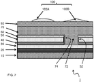
- a barrier 90 is arranged over said photo-electric conversion layer 70.
- Suitable materials for the barrier are metal oxides, such as SiOx and SiNx.
- the barrier 90 may comprise a plurality of layers, such as a stack of inorganic layers having a mutually different composition.
- a combination of inorganic layers and organic layers may be used.
- a barrier 90 may be formed by a first and a second inorganic layer that sandwich an organic layer.
- the materials used for the barrier 90 have a refractive index lower than that of the photo-electric conversion layer 70.
- light in coupling is further improved by a light in coupling structure 100 arranged over the barrier 90.
- the light in coupling structure comprises a plurality of light in coupling elements 102A, 102B.
- semi-spherical or pyramidal shaped light in coupling elements may be used.
- a method of manufacturing a photo-voltaic element is now disclosed with reference to FIG. 1 to 5 .
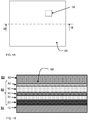
- FIG. 1A, 1B show the intermediate product obtained after a first three steps. Therein FIG. 1A shows a top-view and FIG. 1B shows a cross-section according to IB-IB in FIG. 1A .
- a substrate is 10 is provided in a first step S1.
- a stack of layers is deposited thereon that comprise at least in the order named a first electrode layer 20, a first charge carrier transport layer 30, an insulating layer 40, a second electrode layer 50 and a second charge carrier transport layer.
- the first electrode layer 20 is provided for receiving charge carriers of a first polarity.
- the first electrode layer 20 may for example be an anode, i.e. arranged for receiving holes as the charge carriers.
- the first electrode layer 20 may be a cathode, i.e. arranged for receiving electrons as the charge carriers.
- the first electrode layer 20 is deposited with a PVD (physical vapor deposition) method, for example using E-beam PVD.
- the first electrode layer 20 was provided as a stack of sub-layers obtained by subsequently depositing a first sub-layer of nickel having a thickness of 5 nm, an aluminum layer having a thickness of 190 nm and a second sub-layer of nickel also having a thickness of 5 nm. Then spin-coating (1000 rpm) was used to deposit a NiO layer as the first charge carrier transport layer 30, here a hole transport layer.
- An insulating layer 40 was then deposited in a first and a second stage.
- a first, 100 nm thick, sublayer of SiO x was deposited by electron-beam deposition and in the second stage a second sublayer of SiO x , also having a thickness of 100 nm was deposited by PECVD.
- a second electrode layer 50 here a cathode layer of aluminum at a thickness of 200 nm was formed using the same method and conditions as those applied for the deposition of the aluminum sub-layer of the first electrode layer 20.
- a second charge carrier transport layer 60 here an electron transport layer was then deposited.
- electron-beam vapor deposition was used to deposit a TiO x layer with a thickness of 15 nm of linear titanium dioxide (TiOx).
- the insulating layer 40 and the layers 50, 60 form a sub-stack having an upper surface 64.
- a third step S3 here using spin coating a resist layer 80, here a photo-resist layer having a thickness of 1.6 micron was deposited on this upper surface 64.
- the resist layer may be an imprint-resist layer.
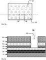
- FIG. 2A, 2B show a subsequent step S4.
- FIG. 2A shows a top-view of an intermediate product resulting from this step S4
- FIG. 2B shows a cross-section according to IIB-IIB in FIG. 2A .
- this subsequent step regularly distributed openings 82 giving access to the upper surface 64 are formed in the resist layer 80.
- contact lithography was used for this purpose.
- samples were prepared having openings with diameter in the range of 0,5 - 5 ⁇ m and a distance between neighboring openings in the range of 1 - 5 ⁇ m. Therewith a pitch between 1 and 10 ⁇ m is obtained.
- the openings having an effective cross-section D in the range of 0.5 to 10 micron, and have an average pitch in the range of 1.1 to 5 times the effective cross-section.
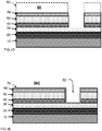
- FIGs. 3A and 3B show a subsequent step S5, wherein material of the sub-stack 40, 50, 60 facing the openings 82 is selectively removed.
- FIG. 3A shows a top-view of the semi-finished product obtained after this step S5 and
- FIG. 3B shows a cross-section according to IIIB-IIIB in FIG. 3A .
- Step S5 involves etching the upper layers 50, 60 by plasma etching. Then the insulating SiO x layer is etched with a further plasma etching process. The photo-resist layer 80 is then fully removed (Step S6), for example by oxygen plasma-etching as illustrated in FIGs. 4A and 4B .
- FIG. 4A is a top-view and FIG. 4B shows a cross-section according to IVB-IVB in FIG. 4A .
- a photo-electric conversion layer 70 is deposited (for example by spin-coating) and cured.
- Optional pre-processing steps, S6A and S6B may be performed after removal of the resist layer 80 and before deposition of the photo-electric conversion layer 70.
- a first optional pre-processing step S6A is illustrated in FIG. 4B .
- an edge surface 52 of the second electrode layer 50 is anodized.
- This edge surface 52 was formed by the step of etching S5.
- This anodization process an insulating layer is formed on the edge surface 52 therewith avoiding a direct contact between the second electrode layer 50 and the photo-electric conversion layer 70.
- FIG. 4C illustrates a second optional pre-processing step S6B.
- an atomic layer deposition process ALD may be used to deposit a thin growth layer 74, e.g. applying a TiO 2 layer with a few sALD cycles.
- FIG. 4D-4G shows an alternative approach for preventing a direct electrical contact between the second electrode layer 50 and the photo-electric conversion layer 70.
- a layer 76 of an insulating material is conformally deposited (Step S6C) on the semi-finished product of FIG. 4D , therewith obtaining the semifinished product of FIG. 4E .
- an anisotropic etch step S6D e.g. a plasma etch step is applied.
- the anisotropic etch step S6D removes the insulating material from the surface of the second charge carrier transport layer 60 and from the surface portions of the first charge carrier transport layer 30 within the openings 82 but keeps a layer of the insulating material on the walls of the openings 82 intact.
- the photo-electric conversion layer can be deposited (S6E) as shown in FIG. 4G .
- the substrate 10 may be removed.
- an electrode layer e.g. the first electrode layer 20 provides sufficient structural integrity.
- mechanical support may be provided by further layers applied on the photo-electric conversion layer 70.
Landscapes
- Engineering & Computer Science (AREA)
- Chemical & Material Sciences (AREA)
- Materials Engineering (AREA)
- Manufacturing & Machinery (AREA)
- Photovoltaic Devices (AREA)
- Life Sciences & Earth Sciences (AREA)
- Sustainable Energy (AREA)
- Sustainable Development (AREA)
Abstract
A photo-voltaic element (1) comprising a stack of layers is provided. The stack of layers at least includes the following layers arranged in the order named: a first electrode layer, a first charge carrier transport layer, an insulating layer, a second electrode layer, an second charge carrier transport layer, and a photo-electric conversion layer. The photo-electric conversion layer (70), comprises a plurality of distributed extensions (72) extending through the second charge carrier transport layer (60), the second electrode layer (50) and the insulating layer (40) to the first charge carrier transport layer (30). The extensions (72) have an effective cross-section Deff in the range of 0.5 to 10 micron, and have an average pitch in the range of 1.1 to 5 times said effective cross-section.
Description
- The present invention pertains to a photo-voltaic element.
- The present invention further pertains to a method of manufacturing the same.
- A photo-voltaic element is disclosed in
CN105140398 that comprises a conductive substrate; a uniform electron transport layer; a dielectric layer; a metal layer; and a perovskite layer as a photo-electric conversion layer. The latter has a plurality of channels through the dielectric layer and the metal layer that contact the electron transport layer. Accordingly the perovskite photo-electric conversion layer has its electric contacts for delivering electrical energy at the same side. Therewith it can be avoided that light to be converted has to pass through an electrode layer, as a result of which it would be attenuated before conversion. - The cited document also presents a method of manufacturing the photo-voltaic element disclosed therein. Therein a substrate is provided of a transparent conductive glass and an electron transport layer is deposited thereon by magnetron sputtering ZnO. Subsequently a layer of dispersed PS pellets having an original diameter of 2 um is deposited resulting in a hexagonal close-packed structure of said PS pellets. The PS ball diameter is subsequently reduced to 1 um by dry etching using RIE. A dielectric layer of Al2O3 is deposited thereon using ALD deposition followed by magneton sputtering of an Au layer. Subsequently, using a solvent and an ultrasonic treatment the PS pellets and the portions of the Al2O3 layer and the Au layer deposited thereon are removed, so that an Au mesh is obtained that is insulated from the electron transport layer. A perovskite layer is spin coated thereon that both contacts the Au mesh and the ZnO electron transport layer.
- It is a first object of the invention to provide a photo-voltaic element with an improved conversion efficiency.
- It is a second object of the invention to provide a method of manufacturing this improved photo-voltaic element.
- In accordance with said first object, according to a first aspect, a photo-voltaic element is provided as claimed in
claim 1. - In accordance with said second object, according to a second aspect, a method of manufacturing a photo-voltaic element is provided as claimed in claim 8.
- The photo-voltaic element is provided as claimed in
claim 1 comprises a stack of layers that at least include in the order named: a first electrode layer, a first charge carrier transport layer, an insulating layer, a second electrode layer, an second charge carrier transport layer, and a photo-electric conversion layer. - The first electrode layer is provided for receiving charge carriers of a first polarity, for example electrons, or alternatively for receiving holes as the charge carrier. The first charge carrier transport layer is provided for transport of charge carriers having the first polarity. E.g. if the first electrode layer is a cathode provided for receiving electrons as the charge carrier then the first charge carrier transport layer is an electron transport layer. Alternatively, if the first electrode layer is an anode provided for receiving holes as the charge carrier then the first charge carrier transport layer is a hole transport layer. The insulating layer may be provided of any sufficiently insulating organic or inorganic material. The second electrode layer is provided for receiving charge carriers of a second polarity opposite to the first polarity. Hence if the first electrode layer is a cathode then the second electrode layer is an anode and vice versa. The second charge carrier transport layer is provided for transport of charge carriers having the second polarity. Accordingly the second charge carrier transport layer is a hole transport layer if the second electrode layer is an anode and an electron transport layer if the second electrode layer is a cathode. The photo-electric conversion layer comprises a plurality of distributed extensions that extend through the second charge carrier transport layer, the second electrode layer and the insulating layer to the first charge carrier transport layer.
- Therewith the photo-electric conversion layer is electrically coupled to both the first charge carrier transport layer and the second charge carrier transport layer. In this arrangement solar radiation R does not need to traverse an electrode layer or a charge carrier transport layer, which contributes to an efficient operation of the photo-voltaic element.
- An optimal conversion efficiency is achieved by the presence of a charge carrier transport layer between the first electrode layer and the photo-electric conversion layer as well as between the second electrode layer and the photo-electric conversion layer.
- The extensions have an effective cross-section Deff in the range of 0.5 to 10 micron, and have an average pitch in the range of 1.1 to 5 times their effective cross-section. The effective cross-section is defined here as the diameter of a circle having an area corresponding to the cross-sectional area AØ of the extensions. I.e.

- The extensions are typically cylindrical. Alternatively the extensions may taper inward or outward. The extensions may have any cross-section, such as circular, square or triangular. Preferably, a circumference O of the extensions is less than 10 times the effective diameter Deff and even more preferably less than 5 times the effective diameter Deff. Therewith an optimum contact surface between the photo-electric conversion layer and the first charge carrier transport layer is achieved with minimum disruption of the intermediary layers, in particular the second electrode layer and the second charge carrier transport layer.
- In an embodiment the photo-electric conversion layer is provided of a perovskite material. Perovskite materials typical have a crystal structure of ABX3, wherein A is an organic cation as methylammonium (CH3NH3)+, B is an inorganic cation, usually lead (II) (Pb2+), and X is a halogen atom such as iodine (I-), chlorine (Cl-) or bromine (Br-). Perovskite materials are particularly advantageous in that they can be processed relatively easily and in that their bandgap can be set to a desired value by a proper choice of the halide content. A typical example is methylammonium lead trihalide (CH3NH3PbX3), with an optical bandgap between 1.5 and 2.3 eV depending on halide content. Another more complex structure example is Cesium -formamidinum lead trihalide (CS0.05(H2NCHNH2)0.95PbI2.85Br0.15) having a bandgap between 1.5 and 2.2 eV. Other metals such as tin may replace the role of Pb in perovskite materials. An example thereof is CH3NH3SnI3. Also combinations of Sn with Pb perovskites having a wider bandgap in the range of 1.2 to 2.2 eV are possible. In another embodiment the photo-electric conversion layer is made of copper indium gallium selenide (CIGS).
- The method as claimed in claim 8 enables manufacturing the photo-voltaic element of
claim 1. The claimed method comprises the steps of: - providing a substrate;
- depositing thereon a stack of layers comprising at least in the order named:
- a first electrode layer for receiving charge carriers of a first polarity;
- a first charge carrier transport layer, for transport of charge carriers having said first polarity;
- an insulating layer;
- a second electrode layer for receiving charge carriers of a second polarity opposite to said first polarity;
- an second charge carrier transport layer, for transport of charge carriers having said second polarity;
- applying a resist layer on said upper surface, wherein said resist layer is provided with a plurality of distributed openings towards said upper surface, the openings having an effective cross-section D in the range of 0.5 to 10 micron, and having an average pitch in the range of 1.1 to 5 times said effective cross-section,
- etching to selectively remove material of the sub-stack facing the openings,
- removing the resist layer subsequent to said etching,
- depositing and curing a photo-electric conversion layer subsequent to said removing.
- The method according to the present invention enables the deposition of a thicker stack of layers on the first charge carrier transport layer than would be possible when using the pellet based approach known from the prior art. In this way the second charge carrier transport layer can be provided, therewith significantly improving efficiency of the photo-voltaic element.
- Various methods may be used for depositing and applying layers. These methods may include spin-coating, printing methods, slot-die coating and vapor deposition methods like physical vapor deposition (e.g. E-beam PVD, Sputter PVD), (spatial) Atomic Layer Deposition ((s)ALD), and chemical vapor deposition (e.g. plasma-enhanced chemical vapor deposition (PECVD)).
- Etching processes may be applied to remove a material (or a part of the material) from a surface either by a chemical reaction generated by the use of a reactive mix of gases (plasma-etching) or by submerging the substrates in a reactive solution where the layer is removed by dissolution or chemical reaction (wet-etching).
- A selective etching is made possible by using a mask that locally protects the underlying layer(s). A patterning in such a mask may be obtained for example by optical lithography wherein light is used to transfer a geometric pattern from a photo-mask to a light sensitive chemical photoresist on the substrate. Also imprinting can be applied to pattern the mask. Alternatively the mask may be directly applied in the desired pattern, for example by printing.
- These and other aspects are described in more detail with reference to the drawing. Therein:
-
FIG. 1A schematically shows a top-view of a semi-finished product obtained during performing a method according to the second aspect, -
FIG. 1B shows a cross-section according to IB-IB inFIG. 1A , -
FIG. 2A shows a top-view corresponding to the area IIA of a semi-finished product obtained after an additional manufacturing step of a method according to the second aspect, -
FIG. 2B shows a cross-section according to IIB-IIB inFIG. 2A , -
FIG. 3A shows a top-view corresponding to the area IIA of a semi-finished product obtained after a further additional manufacturing step of a method according to the second aspect, -
FIG. 3B shows a cross-section according to IIIB-IIIB inFIG. 3A , -
FIG. 4A shows a top-view corresponding to the area IIA of a semi-finished product obtained after a still further additional manufacturing step of a method according to the second aspect, -
FIG. 4B shows a cross-section according to IVB-IVB inFIG. 4A , -
FIG. 4C shows in the same cross-section an optional manufacturing step of a method according to the second aspect, -
FIG. 4D shows in the same cross-section an alternative optional manufacturing step of a method according to the second aspect, -
FIG. 4E shows in the same cross-section a subsequent alternative optional manufacturing step of a method according to the second aspect, -
FIG. 4F shows in the same cross-section an further subsequent alternative optional manufacturing step of a method according to the second aspect, -
FIG. 4G shows in the same cross-section an alternative embodiment resulting from a still further subsequent alternative optional manufacturing step following the step illustrated inFIG. 4F , -
FIG. 5 shows in the same cross-section a first embodiment of a photo-voltaic element according to the first aspect obtained after a further manufacturing step of a method according to the second aspect, -
FIG. 6 shows in the same cross-section a second embodiment of a photo-voltaic element according to the first aspect, -
FIG. 7 shows in the same cross-section a third embodiment of a photo-voltaic element according to the first aspect, -
FIG. 8A shows a top-view corresponding to the area IIA of a fourth embodiment of a photo-voltaic element according to the first aspect, -
FIG. 8B shows a cross-section according to VIIIB-VIIIB inFIG. 8A . -
Fig. 5 schematically shows a photo-voltaic element 1. The photo-voltaic element 1 comprises asubstrate 10 and a stack of layers arranged thereon. Thesubstrate 10 may be formed of a rigid material such as a metal (e.g. steel, copper or aluminum), silicon or glass or of a flexible material such as a polymer, e.g. a polymer like polyethylene terephthalate (PET), polyethylene naphthalate (PEN), or polyimide (PI). Also thin metal or glass are suitable substrates. If the substrate is conducting, an isolating layer may be deposited on that substrate to isolate the electrode from the substrate. Dependent on the application a thickness of the substrate may be selected in the range of a relatively small value e.g. 50 micron and a relatively large value, e.g. a few mm or more. The stack of layers subsequently includes at least afirst electrode layer 20, a first chargecarrier transport layer 30, an insulatinglayer 40, asecond electrode layer 50, an second chargecarrier transport layer 60, and a photo-electric conversion layer 70. - The
first electrode layer 20 is provided for receiving charge carriers of a first polarity. In the embodiment shown thefirst electrode layer 20 is an anode, i.e. arranged for receiving holes as the charge carriers. Dependent on the lateral size of the photo-voltaic element 1 thefirst electrode layer 20 may for example have a thickness in the range of a few tens to a few hundreds of nanometers or even more. In the embodiment shown thefirst electrode layer 20 includes an aluminum sub layer having a thickness of 190 nm, which is sandwiched between a pair of nickel layers, each having a thickness of 5 nm. In another example the first electrode layer is of molybdenum. In an embodiment where the substrate is provided of a metal, it may also serve as afirst electrode layer 20. - In the embodiment shown the first charge
carrier transport layer 30 is a hole transport layer, having a thickness in the range of 10 to 200 nm. In the embodiment shown the hole transport layer is formed by a nickeloxide layer having a thickness of 50 nm. In another example the hole transport layer is formed by a MoSe layer. - An insulating
layer 40 is provided of an organic, e.g. a polymer, or inorganic insulating material, such as a metal oxide. Also a stack of materials can be used. Dependent on the material selected for the insulating layer, it may have a thickness in the range of 10 to 200 nm for example, but also a substantially thicker insulating layer may be applied. In the embodiment shown the insulatinglayer 40 is provided as an SiO2 layer having a thickness of 100 nm. - A
second electrode layer 50 for receiving charge carriers of a second polarity opposite to said first polarity is arranged on the insulatinglayer 40. In this case thesecond electrode layer 50 is a cathode. Any sufficiently conducting material can be used for this purpose at a thickness depending on the lateral size of the photo-voltaic element 1. Typically the thickness of thesecond electrode layer 50 is of the same order of magnitude as the thickness of thefirst electrode layer 20, so that they have approximately the same conductivity and neither of them forms a bottleneck. In the embodiment shown thesecond electrode layer 50 is an aluminum layer with a thickness of 200 nm. In some embodiments thesecond electrode layer 50 may have a thickness greater than that of thefirst electrode layer 20, e.g. 1.5 times a thickness of thefirst electrode layer 20, to compensate for the presence of the openings provided in thesecond electrode layer 50. - A second charge
carrier transport layer 60 for transport of charge carriers having said the second polarity, opposite to the first polarity layer is arranged upon thesecond electrode layer 50. In this case the second chargecarrier transport layer 60 is an electron transport layer. The second chargecarrier transport layer 60, here an electron transport layer may have a thickness in the range of a few nm, e.g. 5 nm to a few tens of nm, e.g. 50 nm. In the embodiment shown the second chargecarrier transport layer 60 is a TiO2 layer having thickness of 15 nm. Other suitable materials for an electron transport layer are for example SnO2, ZrO2 and ZnO:S. - A photo-
electric conversion layer 70 is provided upon the second chargecarrier transport layer 60. The photo-electric conversion layer 70 has a plurality of distributed, typically cylindrical,extensions 72 that extend through the second chargecarrier transport layer 60, thesecond electrode layer 50 and the insulatinglayer 40 to the first chargecarrier transport layer 30. Therewith the photo-electric conversion layer 70 is electrically coupled to both the first chargecarrier transport layer 30 and the second chargecarrier transport layer 60. In this arrangement solar radiation R does not need to traverse an electrode layer or a charge carrier transport layer which contributes to an efficient operation of the photo-voltaic element 1. In the embodiment shown theextensions 72 have an effective cross-section Deff in the range of 0.5 to 10 micron, and have an average pitch in the range of 1.1 to 5 times their effective cross-section. The effective cross-section is defined here as the diameter of a circle having an area corresponding to the cross-sectional area AØ of the extensions.
I.e.
- The extensions may have any cross-section, such as circular, square or triangular. Preferably, a circumference O of the extensions is less than 10 times the effective diameter Deff and even more preferably less than 5 times the effective diameter Deff.
- In the embodiment the photo-electric conversion layer is provided of a perovskite material, such as methylammonium lead trihalide (CH3NH3PbX3), or Cesium-formamidinum lead trihalide (Cs0.05(H2NCHNH2)0.95Pbl2.85Br0.15) .. Alternatively a tin based perovskite material, such as CH3NH3SnI3 may be used. Also more complex perovskite materials may be applied, for example containing a combination of different cations. Also other materials, such as copper indium gallium selenide (CIGS) are suitable.
- In the embodiment shown the
second electrode layer 50 has anodized edge surfaces 52 facing theextensions 72 of the photo-electric conversion layer 70. This avoids direct contact between the second electrode layer and the photo-electric conversion layer. -
FIG. 4G illustrates an alternative embodiment wherein such direct contact is avoided. Therein theopenings 82 are provided with an insulatingwall 78, e.g. of a ceramic material. The specific steps for manufacturing this embodiment are described in more detail below with reference toFIG. 4D to FIG. 4G . -
FIG. 6 shows an embodiment of the photo-voltaic element 1 of the invention wherein anedge portion 22 of an upper surface of thefirst electrode layer 20 is kept free from material of the first chargecarrier transport layer 30 and is provided with a firstelectrical contact 25. Also anedge portion 52 of an upper surface of thesecond electrode layer 50 is kept free from material of the second chargecarrier transport layer 60 and is provided with a secondelectrical contact 55. Another possibility is to remove thecarrier transport layer 30 andisolator 40 with e.g. laser ablation before deposition ofelectrode 50, so a contact can be made fromelectrode 50 toelectrode 20. Also before deposition of charge carrier transport layer 30 a laser step could be used to interrupt theelectrode 20. -
FIGs. 8A and 8B show a further embodiment of a photo-voltaic element according to the invention. ThereinFIG. 8A shows a top-view andFIG. 8B shows a cross-section of a portion of the device according to VIIIB-VIIIB inFIG. 8A . In this further embodiment thefirst electrode layer 20, the first chargecarrier transport layer 30, the insulatinglayer 40 and thesecond electrode layer 50 are provided as a plurality of layer segments. Therein a plurality of lateral sub-stack segments is formed. By way of example two lateral sub-stack segments A,B are shown in this case. However in practice the photo-voltaic element may have a larger number of lateral sub-stack segments C,D, ... e.g. 10 or 100 or more, depending on a required lateral size of the photo-voltaic element. - As shown in
FIG. 8B each layer segment A,B comprises a firstelectrode layer segment transport layer segment layer segment electrode layer segment carrier transport layer 60 and the photo-electric conversion layer 70 are formed as continuous layers. A secondelectrode layer segment 50A of a lateral sub-stack segment A extends over a first electrode layer segment (20B) in a neighboring sub-stack segment B. Therewith an electrical connection is formed between the secondelectrode layer segment 50A of the lateral sub-stack segment A and the firstelectrode layer segment 20B in the neighboring lateral sub-stack segment. In this way the photo-voltaic element is formed as a plurality of serially connected modules, which makes it possible to reduce resistive losses as compared to a photo-voltaic element that is not partitioned into serially connected modules. It could alternatively be contemplated to serially arrange a plurality of smaller photo-voltaic elements. It is however an advantage of the embodiment ofFIG. 8A, 8B that external connection elements are avoided. A photo-voltaic element as shown inFIG. 8A, 8B could for example be provided as a single elongate product applied on a foil, e.g. delivered in a length of tens to hundreds of meter on a roll. - As shown in
FIG. 7 additional layers may be provided. In the embodiment ofFIG. 7 for example abarrier 90 is arranged over said photo-electric conversion layer 70. Suitable materials for the barrier are metal oxides, such as SiOx and SiNx. In practice thebarrier 90 may comprise a plurality of layers, such as a stack of inorganic layers having a mutually different composition. Also a combination of inorganic layers and organic layers may be used. For example abarrier 90 may be formed by a first and a second inorganic layer that sandwich an organic layer. For a good light in coupling it is preferred that the materials used for thebarrier 90 have a refractive index lower than that of the photo-electric conversion layer 70. - In the embodiment shown light in coupling is further improved by a light in
coupling structure 100 arranged over thebarrier 90. In the embodiment shown the light in coupling structure comprises a plurality of light incoupling elements - A method of manufacturing a photo-voltaic element is now disclosed with reference to
FIG. 1 to 5 . -
FIG. 1A, 1B show the intermediate product obtained after a first three steps. ThereinFIG. 1A shows a top-view andFIG. 1B shows a cross-section according to IB-IB inFIG. 1A . - Therein a substrate is 10 is provided in a first step S1. Then in a second step S2 a stack of layers is deposited thereon that comprise at least in the order named a
first electrode layer 20, a first chargecarrier transport layer 30, an insulatinglayer 40, asecond electrode layer 50 and a second charge carrier transport layer. - The
first electrode layer 20 is provided for receiving charge carriers of a first polarity. Thefirst electrode layer 20 may for example be an anode, i.e. arranged for receiving holes as the charge carriers. Alternatively thefirst electrode layer 20 may be a cathode, i.e. arranged for receiving electrons as the charge carriers. In an embodiment thefirst electrode layer 20 is deposited with a PVD (physical vapor deposition) method, for example using E-beam PVD. In this example thefirst electrode layer 20 was provided as a stack of sub-layers obtained by subsequently depositing a first sub-layer of nickel having a thickness of 5 nm, an aluminum layer having a thickness of 190 nm and a second sub-layer of nickel also having a thickness of 5 nm. Then spin-coating (1000 rpm) was used to deposit a NiO layer as the first chargecarrier transport layer 30, here a hole transport layer. - An insulating
layer 40 was then deposited in a first and a second stage. In the first of these stages a first, 100 nm thick, sublayer of SiOx was deposited by electron-beam deposition and in the second stage a second sublayer of SiOx, also having a thickness of 100 nm was deposited by PECVD. Then asecond electrode layer 50, here a cathode layer of aluminum at a thickness of 200 nm was formed using the same method and conditions as those applied for the deposition of the aluminum sub-layer of thefirst electrode layer 20. - A second charge
carrier transport layer 60, here an electron transport layer was then deposited. In this case electron-beam vapor deposition was used to deposit a TiOx layer with a thickness of 15 nm of linear titanium dioxide (TiOx). - The insulating
layer 40 and thelayers upper surface 64. In a third step S3, here using spin coating a resistlayer 80, here a photo-resist layer having a thickness of 1.6 micron was deposited on thisupper surface 64. In other implementations the resist layer may be an imprint-resist layer. -
FIG. 2A, 2B show a subsequent step S4. ThereinFIG. 2A shows a top-view of an intermediate product resulting from this step S4 andFIG. 2B shows a cross-section according to IIB-IIB inFIG. 2A . In this subsequent step regularly distributedopenings 82 giving access to theupper surface 64 are formed in the resistlayer 80. In this embodiment contact lithography was used for this purpose. Using the method described herewith samples were prepared having openings with diameter in the range of 0,5 - 5 µm and a distance between neighboring openings in the range of 1 - 5 µm. Therewith a pitch between 1 and 10 µm is obtained. The openings having an effective cross-section D in the range of 0.5 to 10 micron, and have an average pitch in the range of 1.1 to 5 times the effective cross-section. - Instead of patterning an originally homogeneous resist layer, it is alternatively possible to directly depositing the resist layer in the desired pattern, for example using a printing technique.
-
FIGs. 3A and 3B show a subsequent step S5, wherein material of the sub-stack 40, 50, 60 facing theopenings 82 is selectively removed. ThereinFIG. 3A shows a top-view of the semi-finished product obtained after this step S5 andFIG. 3B shows a cross-section according to IIIB-IIIB inFIG. 3A . Step S5 involves etching theupper layers layer 80 is then fully removed (Step S6), for example by oxygen plasma-etching as illustrated inFIGs. 4A and 4B . ThereinFIG. 4A is a top-view andFIG. 4B shows a cross-section according to IVB-IVB inFIG. 4A . - As shown in
FIG. 5 , in a step S7, subsequent to this step S6, a photo-electric conversion layer 70 is deposited (for example by spin-coating) and cured.
Optional pre-processing steps, S6A and S6B may be performed after removal of the resistlayer 80 and before deposition of the photo-electric conversion layer 70. - A first optional pre-processing step S6A is illustrated in
FIG. 4B . Therein anedge surface 52 of thesecond electrode layer 50 is anodized. Thisedge surface 52 was formed by the step of etching S5. This anodization process an insulating layer is formed on theedge surface 52 therewith avoiding a direct contact between thesecond electrode layer 50 and the photo-electric conversion layer 70. -
FIG. 4C illustrates a second optional pre-processing step S6B. Therein to facilitate the deposition in step S7, an atomic layer deposition process (ALD) may be used to deposit athin growth layer 74, e.g. applying a TiO2 layer with a few sALD cycles. -
FIG. 4D-4G shows an alternative approach for preventing a direct electrical contact between thesecond electrode layer 50 and the photo-electric conversion layer 70. After removal (S6) of the patterned resistlayer 80 as shown inFIG. 4D , alayer 76 of an insulating material is conformally deposited (Step S6C) on the semi-finished product ofFIG. 4D , therewith obtaining the semifinished product ofFIG. 4E . Then an anisotropic etch step S6D, e.g. a plasma etch step is applied. The anisotropic etch step S6D removes the insulating material from the surface of the second chargecarrier transport layer 60 and from the surface portions of the first chargecarrier transport layer 30 within theopenings 82 but keeps a layer of the insulating material on the walls of theopenings 82 intact. Subsequent to this step S6D the photo-electric conversion layer can be deposited (S6E) as shown inFIG. 4G . - Upon completion the
substrate 10 may be removed. For example this may be the case if an electrode layer, e.g. thefirst electrode layer 20 provides sufficient structural integrity. Alternatively, or in addition mechanical support may be provided by further layers applied on the photo-electric conversion layer 70. - While the invention has been illustrated and described in detail in the drawings and foregoing description, such illustration and description are to be considered illustrative and exemplary and not restrictive; the invention is not limited to the disclosed embodiments. Other variations to the disclosed embodiments can be understood and effected by those skilled in the art in practicing the claimed invention, from a study of the drawings, the disclosure and the appended claims.
- In the claims the word "comprising" does not exclude other elements or steps, and the indefinite article "a" or "an" does not exclude a plurality. A single processor or other unit may fulfill the functions of several items recited in the claims. The mere fact that certain measures are recited in mutually different claims does not indicate that a combination of these measures cannot be used to advantage. Any reference signs in the claims should not be construed as limiting the scope.
Claims (17)
- A photo-voltaic element (1) comprising a stack of layers, the stack of layers at least including the following layers arranged in the order named:- a first electrode layer (20) for receiving charge carriers of a first polarity,- a first charge carrier transport layer (30), for transport of charge carriers having said first polarity,- an insulating layer (40),- a second electrode layer (50) for receiving charge carriers of a second polarity opposite to said first polarity,- a second charge carrier transport layer (60), for transport of charge carriers having said second polarity,- a photo-electric conversion layer (70), comprising a plurality of distributed extensions (72) extending through said second charge carrier transport layer (60), said second electrode layer (50) and said insulating layer (40) to the first charge carrier transport layer (30), the extensions (72) having an effective cross-section Deff in the range of 0.5 to 10 micron, and having an average pitch in the range of 1.1 to 5 times said effective cross-section.
- The photo-voltaic element according to claim 1, wherein said second electrode layer (50) has anodized edge surfaces (52) facing the extensions (72) of the photo-electric conversion layer (70).
- The photo-voltaic element according to claim 1, wherein an insulating material is provided around said extensions (72), forming an insulating wall (78) between said second electrode layer (50) and said photo-electric conversion layer (70).
- The photo-voltaic element according to claim 1, 2 or 3, further comprising a growth layer (74) at an interface between said photo-electric conversion layer (70) and said second charge carrier transport layer (60) as well as at an interface between said extensions (72) of the photo-electric conversion layer and each of edge surfaces of said second charge carrier transport layer (60), said second electrode layer (50) and said insulating layer (40) and at an interface between said extensions of the photo-electric conversion layer and the first charge carrier transport layer (30).
- The photo-voltaic element according to one of the previous claims, wherein the photo-electric conversion layer is provided of a perovskite material.
- The photo-voltaic element according to one of the previous claims, wherein the photo-electric conversion layer is made of copper indium gallium selenide (CIGS).
- The photo-voltaic element according to one of the previous claims, wherein an edge portion of an upper surface of the first electrode layer (20) is kept free from material of the first charge carrier transport layer (30) and is provided with a first electrical contact (25) and or an edge portion of an upper surface of the second electrode layer (50) is kept free from material of the second charge carrier transport layer (60) and is provided with a second electrical contact (55).
- The photo-voltaic element according to one of the previous claims, wherein said first electrode layer (20), said first charge carrier transport layer (30), said insulating layer (40) and said second electrode layer (50) are provided as a plurality of layer segments, wherein a plurality of lateral sub-stack segments each comprise a respective first electrode layer segment (20A, 20B), a first charge carrier transport layer segment (30A, 30B), an insulating layer segment (40A, 40B) and a second electrode layer segment (50A, 50B), wherein a second electrode layer segment (50A) of a lateral substack segment extends over a first electrode layer segment (20B) in a neighboring sub-stack segment, therewith forming an electrical connection between said second electrode layer segment (50A) of said lateral sub-stack segment and said first electrode layer segment (20B) in said neighboring lateral sub-stack segment.
- Method of manufacturing a photo-voltaic element comprising the steps of:- providing (S1) a substrate (10);- depositing (S2) thereon a stack of layers comprising at least in the order named:- a first electrode layer (20) for receiving charge carriers of a first polarity;- a first charge carrier transport layer (30), for transport of charge carriers having said first polarity;- an insulating layer (40);- a second electrode layer (50) for receiving charge carriers of a second polarity opposite to said first polarity;- an second charge carrier transport layer (60), for transport of charge carriers having said second polarity;wherein the insulating layer and layers subsequently deposited in this step form a substack having an upper surface (64),- applying (S3) a resist layer (80) on said upper surface, wherein said resist layer is provided (S4) with a plurality of distributed openings (82) towards said upper surface, the openings having an effective cross-section D in the range of 0.5 to 10 micron, and having an average pitch in the range of 1.1 to 5 times said effective cross-section,- etching (S5) to selectively remove material of the sub-stack facing the openings (82),- removing (S6) the resist layer subsequent to said etching,- depositing (S7) and curing a photo-electric conversion layer (70) subsequent to said removing.
- The method according to claim 9, further comprising anodizing (S6A) an edge surface of the second electrode layer resulting from said etching, said anodizing being performed prior to the step of depositing the photo-electric conversion layer.
- The method according to claim 9, further comprising conformally depositing (S6C) a layer (76) of an insulating material subsequent to said step of etching (S5) and anisotropically etching (S6D) said layer (76) to removes the insulating material from the surface of the second charge carrier transport layer (60) and from the surface portions of the first charge carrier transport layer (30) within the openings (82) while keeping a layer (78) of the insulating material on the walls of the openings (82) intact.
- The method according to claim 9, 10 or 11, further comprising depositing (S6B) a growth layer (74) subsequent to said step of etching (S5) and prior to the step of depositing (S7) the photo-electric conversion layer.
- The method according to one of the claims 9-12, further comprising depositing a barrier (90) over said photo-electric conversion layer.
- The method according to claim 13, wherein said barrier (90) has a refractive index lower than a refractive index of said photo-electric conversion layer.
- The method according to claim 13 or 14, comprising applying a light in coupling structure (100) over said barrier.
- The method according to claim 15, wherein said light in coupling structure comprises a plurality of light in coupling elements.
- The method according to one of the claims 9-16, wherein the photo-electric conversion layer (70) is provided of a perovskite material or of copper indium gallium selenide (CIGS).
Priority Applications (8)
| Application Number | Priority Date | Filing Date | Title |
|---|---|---|---|
| EP17166454.3A EP3389096A1 (en) | 2017-04-13 | 2017-04-13 | Photo-voltaic element and method of manufacturing the same |
| CN201880034554.XA CN110692141B (en) | 2017-04-13 | 2018-04-12 | Photovoltaic elements and methods of manufacturing same |
| US16/604,756 US20200381568A1 (en) | 2017-04-13 | 2018-04-12 | Photo-voltaic element and method of manufacturing the same |
| PCT/NL2018/050224 WO2018190711A1 (en) | 2017-04-13 | 2018-04-12 | Photo-voltaic element and method of manufacturing the same |
| RU2019132233A RU2019132233A (en) | 2017-04-13 | 2018-04-12 | PHOTOVOLTAIC ELEMENT AND METHOD OF ITS MANUFACTURE |
| EP18723612.0A EP3610514B1 (en) | 2017-04-13 | 2018-04-12 | Photovoltaic element and method of manufacturing the same |
| TW107112776A TW201904080A (en) | 2017-04-13 | 2018-04-13 | Photovoltaic device and method of manufacturing same |
| US18/370,622 US20240105866A1 (en) | 2017-04-13 | 2023-09-20 | Photo-voltaic element and method of manufacturing the same |
Applications Claiming Priority (1)
| Application Number | Priority Date | Filing Date | Title |
|---|---|---|---|
| EP17166454.3A EP3389096A1 (en) | 2017-04-13 | 2017-04-13 | Photo-voltaic element and method of manufacturing the same |
Publications (1)
| Publication Number | Publication Date |
|---|---|
| EP3389096A1 true EP3389096A1 (en) | 2018-10-17 |
Family
ID=58548596
Family Applications (2)
| Application Number | Title | Priority Date | Filing Date |
|---|---|---|---|
| EP17166454.3A Withdrawn EP3389096A1 (en) | 2017-04-13 | 2017-04-13 | Photo-voltaic element and method of manufacturing the same |
| EP18723612.0A Active EP3610514B1 (en) | 2017-04-13 | 2018-04-12 | Photovoltaic element and method of manufacturing the same |
Family Applications After (1)
| Application Number | Title | Priority Date | Filing Date |
|---|---|---|---|
| EP18723612.0A Active EP3610514B1 (en) | 2017-04-13 | 2018-04-12 | Photovoltaic element and method of manufacturing the same |
Country Status (6)
| Country | Link |
|---|---|
| US (2) | US20200381568A1 (en) |
| EP (2) | EP3389096A1 (en) |
| CN (1) | CN110692141B (en) |
| RU (1) | RU2019132233A (en) |
| TW (1) | TW201904080A (en) |
| WO (1) | WO2018190711A1 (en) |
Cited By (3)
| Publication number | Priority date | Publication date | Assignee | Title |
|---|---|---|---|---|
| EP3654389A1 (en) * | 2018-11-16 | 2020-05-20 | Nederlandse Organisatie voor toegepast- natuurwetenschappelijk onderzoek TNO | Photovoltaic device and method of manufacturing the same |
| CN113380950A (en) * | 2021-05-12 | 2021-09-10 | 郑州轻工业大学 | Back contact perovskite solar cell and preparation method thereof |
| US20220115547A1 (en) * | 2020-10-09 | 2022-04-14 | Alliance For Sustainable Energy, Llc | All-back-contact perovskite solar cells |
Families Citing this family (9)
| Publication number | Priority date | Publication date | Assignee | Title |
|---|---|---|---|---|
| EP3840059A1 (en) | 2019-12-19 | 2021-06-23 | Nederlandse Organisatie voor toegepast- natuurwetenschappelijk Onderzoek TNO | Semi-translucent photovoltaic device and method of manufacturing the same |
| CN111312901A (en) * | 2020-02-25 | 2020-06-19 | 南开大学 | Stacking interdigital full back contact perovskite solar cell and preparation method thereof |
| CN111312900A (en) * | 2020-02-25 | 2020-06-19 | 南开大学 | Parallel interdigital full back contact perovskite solar cell and preparation method thereof |
| CN111293222B (en) * | 2020-02-25 | 2024-03-22 | 南开大学 | Positive interdigital full back contact perovskite solar cell and preparation method thereof |
| CN111599921B (en) * | 2020-04-09 | 2023-07-21 | 南开大学 | Nested full back contact perovskite solar cell and preparation method thereof |
| WO2022174055A1 (en) * | 2021-02-12 | 2022-08-18 | First Solar, Inc. | Multilayer back contacts for perovskite photovoltaic devices |
| CN116964757A (en) * | 2021-03-04 | 2023-10-27 | 联邦科学和工业研究组织 | Methods for forming electrode interconnections in integrated multilayer thin film electronic devices |
| CN113540358B (en) * | 2021-06-28 | 2023-04-25 | 苏州大学 | Lead-free tin-based perovskite indoor photovoltaic device and preparation method thereof |
| TWI808860B (en) | 2022-08-05 | 2023-07-11 | 位速科技股份有限公司 | Thin film photovoltaic structure and method of making the same |
Citations (4)
| Publication number | Priority date | Publication date | Assignee | Title |
|---|---|---|---|---|
| US20150123094A1 (en) * | 2012-05-09 | 2015-05-07 | Lg Chem, Ltd. | Organic electrochemical device, and method for manufacturing same |
| CN105140398A (en) | 2015-07-02 | 2015-12-09 | 南京大学 | Back-contact perovskite solar cell |
| WO2016038825A1 (en) * | 2014-09-10 | 2016-03-17 | Sharp Kabushiki Kaisha | Back contact perovskite solar cell |
| WO2017060700A1 (en) * | 2015-10-06 | 2017-04-13 | Oxford University Innovation Limited | Device architecture |
Family Cites Families (2)
| Publication number | Priority date | Publication date | Assignee | Title |
|---|---|---|---|---|
| EP2698836A1 (en) * | 2012-08-17 | 2014-02-19 | Nederlandse Organisatie voor toegepast -natuurwetenschappelijk onderzoek TNO | Foil, electro-optic component and method of manufacturing these |
| US9425396B2 (en) * | 2013-11-26 | 2016-08-23 | Hunt Energy Enterprises L.L.C. | Perovskite material layer processing |
-
2017
- 2017-04-13 EP EP17166454.3A patent/EP3389096A1/en not_active Withdrawn
-
2018
- 2018-04-12 CN CN201880034554.XA patent/CN110692141B/en active Active
- 2018-04-12 WO PCT/NL2018/050224 patent/WO2018190711A1/en not_active Ceased
- 2018-04-12 US US16/604,756 patent/US20200381568A1/en not_active Abandoned
- 2018-04-12 EP EP18723612.0A patent/EP3610514B1/en active Active
- 2018-04-12 RU RU2019132233A patent/RU2019132233A/en unknown
- 2018-04-13 TW TW107112776A patent/TW201904080A/en unknown
-
2023
- 2023-09-20 US US18/370,622 patent/US20240105866A1/en active Pending
Patent Citations (4)
| Publication number | Priority date | Publication date | Assignee | Title |
|---|---|---|---|---|
| US20150123094A1 (en) * | 2012-05-09 | 2015-05-07 | Lg Chem, Ltd. | Organic electrochemical device, and method for manufacturing same |
| WO2016038825A1 (en) * | 2014-09-10 | 2016-03-17 | Sharp Kabushiki Kaisha | Back contact perovskite solar cell |
| CN105140398A (en) | 2015-07-02 | 2015-12-09 | 南京大学 | Back-contact perovskite solar cell |
| WO2017060700A1 (en) * | 2015-10-06 | 2017-04-13 | Oxford University Innovation Limited | Device architecture |
Cited By (6)
| Publication number | Priority date | Publication date | Assignee | Title |
|---|---|---|---|---|
| EP3654389A1 (en) * | 2018-11-16 | 2020-05-20 | Nederlandse Organisatie voor toegepast- natuurwetenschappelijk onderzoek TNO | Photovoltaic device and method of manufacturing the same |
| WO2020101494A1 (en) * | 2018-11-16 | 2020-05-22 | Nederlandse Organisatie Voor Toegepast- Natuurwetenschappelijk Onderzoek Tno | Photovoltaic device and method of manufacturing the same |
| US11476307B2 (en) | 2018-11-16 | 2022-10-18 | Nederlandse Organisatie Voor Toegepast-Natuurwetenschappelijk Onderzoek Tno | Photovoltaic device and method of manufacturing the same |
| US20220115547A1 (en) * | 2020-10-09 | 2022-04-14 | Alliance For Sustainable Energy, Llc | All-back-contact perovskite solar cells |
| US11742440B2 (en) * | 2020-10-09 | 2023-08-29 | Alliance For Sustainable Energy, Llc | All-back-contact perovskite solar cells |
| CN113380950A (en) * | 2021-05-12 | 2021-09-10 | 郑州轻工业大学 | Back contact perovskite solar cell and preparation method thereof |
Also Published As
| Publication number | Publication date |
|---|---|
| CN110692141A (en) | 2020-01-14 |
| TW201904080A (en) | 2019-01-16 |
| EP3610514B1 (en) | 2021-06-09 |
| US20240105866A1 (en) | 2024-03-28 |
| CN110692141B (en) | 2023-10-31 |
| WO2018190711A1 (en) | 2018-10-18 |
| EP3610514A1 (en) | 2020-02-19 |
| WO2018190711A8 (en) | 2019-10-31 |
| RU2019132233A (en) | 2021-05-13 |
| US20200381568A1 (en) | 2020-12-03 |
Similar Documents
| Publication | Publication Date | Title |
|---|---|---|
| US20240105866A1 (en) | Photo-voltaic element and method of manufacturing the same | |
| EP3121840B1 (en) | Thin-film transistor and preparation method therefor, array substrate, and display panel | |
| US8686459B2 (en) | Light-transmitting metal electrode and process for production thereof | |
| WO2022184038A1 (en) | Manufacturing method for electrode of photovoltaic cell, and photovoltaic cell | |
| CN113258006B (en) | Perovskite battery structure containing grid lines and preparation method thereof | |
| EP2908348A1 (en) | Thin film transistor and manufacturing method thereof, array substrate and display device | |
| WO2018126508A1 (en) | Method for manufacturing tft substrate | |
| CN101432888B (en) | Ultra lightweight photovoltaic device and method for its manufacture | |
| EP3599642A1 (en) | Photovoltaic device and method of manufacturing the same | |
| KR101682501B1 (en) | Transparant electrode containing silver nanowire-patterned layer and graphene layer, and manufacturing method thereof | |
| CN101803038B (en) | Thin film solar cell element and manufacturing method thereof | |
| US3671819A (en) | Metal-insulator structures and method for forming | |
| CN106935668A (en) | Transparency conducting layer stacking and its manufacture method comprising pattern metal functional layer | |
| KR20190099903A (en) | Method of patterning a hybrid transparent electrode | |
| EP3827465B1 (en) | Photovoltaic device and method of manufacturing the same | |
| US10121990B2 (en) | Organic light emitting devices and methods of fabricating the same | |
| WO2019227804A1 (en) | Solar cell and preparation method therefor | |
| CN107513723A (en) | Method for reducing opening potential of photoelectrochemical decomposed water of Ni/n-Si photoanode | |
| US10692889B2 (en) | Thin-film transistor array substrate and method of manufacturing the same, as well as display device | |
| CN113571539A (en) | Display panel manufacturing method and display panel | |
| CN106981456B (en) | Manufacturing method of TFT substrate | |
| JP2012054520A (en) | Semiconductor device and method of manufacturing the same | |
| CN210743965U (en) | MSM photosensitive detector and display substrate | |
| WO2017215710A1 (en) | Semiconductor component with front and rear-sided electrodes and method for the production thereof | |
| CN117729824A (en) | BC battery with spacer structure and manufacturing method |
Legal Events
| Date | Code | Title | Description |
|---|---|---|---|
| PUAI | Public reference made under article 153(3) epc to a published international application that has entered the european phase |
Free format text: ORIGINAL CODE: 0009012 |
|
| AK | Designated contracting states |
Kind code of ref document: A1 Designated state(s): AL AT BE BG CH CY CZ DE DK EE ES FI FR GB GR HR HU IE IS IT LI LT LU LV MC MK MT NL NO PL PT RO RS SE SI SK SM TR |
|
| AX | Request for extension of the european patent |
Extension state: BA ME |
|
| STAA | Information on the status of an ep patent application or granted ep patent |
Free format text: STATUS: THE APPLICATION IS DEEMED TO BE WITHDRAWN |
|
| 18D | Application deemed to be withdrawn |
Effective date: 20190418 |