EP3388917A2 - Selecting an aspect ratio for current monitoring - Google Patents
Selecting an aspect ratio for current monitoring Download PDFInfo
- Publication number
- EP3388917A2 EP3388917A2 EP18164350.3A EP18164350A EP3388917A2 EP 3388917 A2 EP3388917 A2 EP 3388917A2 EP 18164350 A EP18164350 A EP 18164350A EP 3388917 A2 EP3388917 A2 EP 3388917A2
- Authority
- EP
- European Patent Office
- Prior art keywords
- circuitry
- electrical current
- trimming
- branch
- aspect ratio
- Prior art date
- Legal status (The legal status is an assumption and is not a legal conclusion. Google has not performed a legal analysis and makes no representation as to the accuracy of the status listed.)
- Granted
Links
Images



Classifications
-
- G—PHYSICS
- G05—CONTROLLING; REGULATING
- G05F—SYSTEMS FOR REGULATING ELECTRIC OR MAGNETIC VARIABLES
- G05F1/00—Automatic systems in which deviations of an electric quantity from one or more predetermined values are detected at the output of the system and fed back to a device within the system to restore the detected quantity to its predetermined value or values, i.e. retroactive systems
- G05F1/10—Regulating voltage or current
- G05F1/46—Regulating voltage or current wherein the variable actually regulated by the final control device is DC
- G05F1/56—Regulating voltage or current wherein the variable actually regulated by the final control device is DC using semiconductor devices in series with the load as final control devices
- G05F1/575—Regulating voltage or current wherein the variable actually regulated by the final control device is DC using semiconductor devices in series with the load as final control devices characterised by the feedback circuit
-
- H—ELECTRICITY
- H02—GENERATION; CONVERSION OR DISTRIBUTION OF ELECTRIC POWER
- H02M—APPARATUS FOR CONVERSION BETWEEN AC AND AC, BETWEEN AC AND DC, OR BETWEEN DC AND DC, AND FOR USE WITH MAINS OR SIMILAR POWER SUPPLY SYSTEMS; CONVERSION OF DC OR AC INPUT POWER INTO SURGE OUTPUT POWER; CONTROL OR REGULATION THEREOF
- H02M1/00—Details of apparatus for conversion
- H02M1/08—Circuits specially adapted for the generation of control voltages for semiconductor devices incorporated in static converters
- H02M1/088—Circuits specially adapted for the generation of control voltages for semiconductor devices incorporated in static converters for the simultaneous control of series or parallel connected semiconductor devices
-
- G—PHYSICS
- G01—MEASURING; TESTING
- G01R—MEASURING ELECTRIC VARIABLES; MEASURING MAGNETIC VARIABLES
- G01R1/00—Details of instruments or arrangements of the types included in groups G01R5/00 - G01R13/00 and G01R31/00
- G01R1/20—Modifications of basic electric elements for use in electric measuring instruments; Structural combinations of such elements with such instruments
-
- G—PHYSICS
- G01—MEASURING; TESTING
- G01R—MEASURING ELECTRIC VARIABLES; MEASURING MAGNETIC VARIABLES
- G01R19/00—Arrangements for measuring currents or voltages or for indicating presence or sign thereof
- G01R19/0092—Measuring current only
-
- H—ELECTRICITY
- H02—GENERATION; CONVERSION OR DISTRIBUTION OF ELECTRIC POWER
- H02M—APPARATUS FOR CONVERSION BETWEEN AC AND AC, BETWEEN AC AND DC, OR BETWEEN DC AND DC, AND FOR USE WITH MAINS OR SIMILAR POWER SUPPLY SYSTEMS; CONVERSION OF DC OR AC INPUT POWER INTO SURGE OUTPUT POWER; CONTROL OR REGULATION THEREOF
- H02M3/00—Conversion of DC power input into DC power output
- H02M3/02—Conversion of DC power input into DC power output without intermediate conversion into AC
-
- H—ELECTRICITY
- H02—GENERATION; CONVERSION OR DISTRIBUTION OF ELECTRIC POWER
- H02M—APPARATUS FOR CONVERSION BETWEEN AC AND AC, BETWEEN AC AND DC, OR BETWEEN DC AND DC, AND FOR USE WITH MAINS OR SIMILAR POWER SUPPLY SYSTEMS; CONVERSION OF DC OR AC INPUT POWER INTO SURGE OUTPUT POWER; CONTROL OR REGULATION THEREOF
- H02M3/00—Conversion of DC power input into DC power output
- H02M3/02—Conversion of DC power input into DC power output without intermediate conversion into AC
- H02M3/04—Conversion of DC power input into DC power output without intermediate conversion into AC by static converters
- H02M3/10—Conversion of DC power input into DC power output without intermediate conversion into AC by static converters using discharge tubes with control electrode or semiconductor devices with control electrode
- H02M3/145—Conversion of DC power input into DC power output without intermediate conversion into AC by static converters using discharge tubes with control electrode or semiconductor devices with control electrode using devices of a triode or transistor type requiring continuous application of a control signal
- H02M3/155—Conversion of DC power input into DC power output without intermediate conversion into AC by static converters using discharge tubes with control electrode or semiconductor devices with control electrode using devices of a triode or transistor type requiring continuous application of a control signal using semiconductor devices only
- H02M3/156—Conversion of DC power input into DC power output without intermediate conversion into AC by static converters using discharge tubes with control electrode or semiconductor devices with control electrode using devices of a triode or transistor type requiring continuous application of a control signal using semiconductor devices only with automatic control of output voltage or current, e.g. switching regulators
- H02M3/158—Conversion of DC power input into DC power output without intermediate conversion into AC by static converters using discharge tubes with control electrode or semiconductor devices with control electrode using devices of a triode or transistor type requiring continuous application of a control signal using semiconductor devices only with automatic control of output voltage or current, e.g. switching regulators including plural semiconductor devices as final control devices for a single load
-
- H—ELECTRICITY
- H03—ELECTRONIC CIRCUITRY
- H03K—PULSE TECHNIQUE
- H03K17/00—Electronic switching or gating, i.e. not by contact-making and –breaking
- H03K17/08—Modifications for protecting switching circuit against overcurrent or overvoltage
- H03K17/082—Modifications for protecting switching circuit against overcurrent or overvoltage by feedback from the output to the control circuit
- H03K17/0822—Modifications for protecting switching circuit against overcurrent or overvoltage by feedback from the output to the control circuit in field-effect transistor switches
-
- H—ELECTRICITY
- H02—GENERATION; CONVERSION OR DISTRIBUTION OF ELECTRIC POWER
- H02M—APPARATUS FOR CONVERSION BETWEEN AC AND AC, BETWEEN AC AND DC, OR BETWEEN DC AND DC, AND FOR USE WITH MAINS OR SIMILAR POWER SUPPLY SYSTEMS; CONVERSION OF DC OR AC INPUT POWER INTO SURGE OUTPUT POWER; CONTROL OR REGULATION THEREOF
- H02M1/00—Details of apparatus for conversion
- H02M1/0003—Details of control, feedback or regulation circuits
- H02M1/0009—Devices or circuits for detecting current in a converter
-
- H—ELECTRICITY
- H02—GENERATION; CONVERSION OR DISTRIBUTION OF ELECTRIC POWER
- H02M—APPARATUS FOR CONVERSION BETWEEN AC AND AC, BETWEEN AC AND DC, OR BETWEEN DC AND DC, AND FOR USE WITH MAINS OR SIMILAR POWER SUPPLY SYSTEMS; CONVERSION OF DC OR AC INPUT POWER INTO SURGE OUTPUT POWER; CONTROL OR REGULATION THEREOF
- H02M7/00—Conversion of AC power input into DC power output; Conversion of DC power input into AC power output
- H02M7/42—Conversion of DC power input into AC power output without possibility of reversal
- H02M7/44—Conversion of DC power input into AC power output without possibility of reversal by static converters
- H02M7/48—Conversion of DC power input into AC power output without possibility of reversal by static converters using discharge tubes with control electrode or semiconductor devices with control electrode
- H02M7/53—Conversion of DC power input into AC power output without possibility of reversal by static converters using discharge tubes with control electrode or semiconductor devices with control electrode using devices of a triode or transistor type requiring continuous application of a control signal
- H02M7/537—Conversion of DC power input into AC power output without possibility of reversal by static converters using discharge tubes with control electrode or semiconductor devices with control electrode using devices of a triode or transistor type requiring continuous application of a control signal using semiconductor devices only, e.g. single switched pulse inverters
-
- H—ELECTRICITY
- H03—ELECTRONIC CIRCUITRY
- H03K—PULSE TECHNIQUE
- H03K2217/00—Indexing scheme related to electronic switching or gating, i.e. not by contact-making or -breaking covered by H03K17/00
- H03K2217/0027—Measuring means of, e.g. currents through or voltages across the switch
Definitions
- This disclosure relates to power electronics circuitry.
- a sensing switch may be positioned in parallel with a power switch and configured to mirror the electrical current conducted by the power switch.
- the ratio of the electrical current conducted by the power switch to the electrical current conducted by the sensing switch may be expressed as N : 1.
- the actual value of N in a device may be different than the target value of N in the device.
- the ratio of electrical currents may be based on the ratio of the sizes of the two switches.
- This disclosure describes techniques for generating a monitored electrical current that is indicative of the electrical current conducted by a power switch.
- the techniques of this disclosure include selecting an aspect ratio for trimming circuitry.
- the trimming circuitry may generate the monitored electrical current based on its aspect ratio and based on the electrical current conducted by the sensing switch. Based on the results of a test of the monitored electrical current, a technician or processing circuitry may select an aspect ratio for the trimming circuitry. Therefore, the monitored electrical current generated by the trimming circuitry may more accurately reflect the target ratio of the electrical current conducted by the power switch to the electrical current conducted by the sensing switch.
- a device including a power switch, a sensing switch configured to conduct an electrical current based on an electrical current conducted by the power switch.
- the device also includes trimming circuitry configured to generate a monitored electrical current based on an aspect ratio of the trimming circuitry and based on the electrical current conducted by the sensing switch, wherein the aspect ratio of the trimming circuitry is adjustable.
- a method is for monitoring an electrical current conducted by a power switch, where the method includes monitoring an electrical current generated by trimming circuitry, wherein the trimming circuitry is configured to generate the monitored electrical current based on an aspect ratio of the trimming circuitry and based on an electrical current conducted by a sensing switch, and wherein the sensing switch is configured to conduct the electrical current based on an electrical current conducted by the power switch.
- the method further includes controlling the aspect ratio of the trimming circuitry based on the monitored electrical current generated by the trimming circuitry.
- a power conversion system includes half-bridge circuitry including a high-side power switch and a low-side power switch.
- the power conversion system further includes a high-side sensing switch configured to conduct an electrical current based on an electrical current conducted by the high-side power switch and a low-side sensing switch configured to conduct an electrical current based on an electrical current conducted by the low-side power switch.
- the power conversion system also includes trimming circuitry configured to generate a monitored electrical current based on an aspect ratio of the trimming circuitry and based on the electrical current conducted by the high-side sensing switch or the electrical current conducted by the low-side sensing switch, wherein the aspect ratio of the trimming circuitry is adjustable.
- a device of this disclosure may include one or more monolithic mirror structures.
- the ratio between the power switch electrical current and the monitored electrical current may be adjustable by several methods and/or configurations. By adjusting the current ratio, a device of this disclosure may generate a more reliable monitored electrical current, which may allow more accurate monitoring of the power switch electrical current, along with lower power dissipation.
- a device of this disclosure may move the trimming operation from the power switch to front-end circuitry such as trimming circuitry.
- the trimming of the current ratio may not be limited by the voltage drop of the metallization on the power switch, which may possibly increase the trimming range.
- the temperature of the device may have a relatively small effect on the operation of the trimming circuitry because it employs a single "tapping point" which makes the trimming circuitry, ideally, temperature independent. Other arrangements including more than one tapping point may, in some examples, depend on the temperature of the components. It may also be possible to trim the high-side current ratio and to match it to the low-side current ratio, for applications that include a half bridge circuit. Moreover, the device may need only one tapping point contacting the source of the power switch, reducing the number of pads in the device.
- Other methods for adjusting a monitored electrical current may include complicated circuitry that takes up more space on a semiconductor die, as compared to the operational amplifiers and trimming circuitry of this disclosure. Other methods may also have greater dependence on temperature than the methods of this disclosure. Thus, in some examples, the techniques of this disclosure may allow for smaller and more accurate devices.
- a device of this disclosure may have several unique ratios between devices and circuits.
- the “aspect ratio” of the trimming circuitry may be defined as the ratio of the number of active transistors in one branch of the trimming circuitry to the number of active transistors in another branch of the trimming circuitry.
- the “aspect ratio” may also be defined as the ratio of the electrical current through one branch of the trimming circuitry to the electrical current through another branch of the trimming circuitry.
- the “aspect ratio” of the trimming circuitry may be represented herein as L : M or M : L , where L is the number of active transistors in one branch and M is the number of active transistors in another branch.
- the trimming circuitry may include more than two branches, and one of the branches may include a single active transistor.
- the ratio of the single-transistor branch to the other branches may be represented as 1 : L and 1 : M.
- the ratios of 1 : L and 1 : M are not referred to as aspect ratios herein.
- a device of this disclosure may also include a ratio of the power switch to the sensing switch, which may be represented as N : 1, where the power switch is N times larger than the sensing switch and/or include N times more modules or cells than the sensing switch.
- the electrical current conducted by the power switch may also be N times larger than the electrical current conducted by the sensing switch. This disclosure may not refer to the ratio of N : 1 as an aspect ratio.
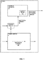
- FIG. 1 is a conceptual block diagram of a device 2 including trimming circuitry 10 configured to generate a monitored electrical current 14 based on an aspect ratio 12 of the trimming circuitry 10 and the electrical current 8B conducted by a sensing switch 6, in accordance with some examples of this disclosure.
- Device 2 includes power switch 4, sensing switch 6, and trimming circuitry 10.
- Device 2 may be a power electronics device, an analog electrical device, an embedded system, an integrated circuit (IC) device, a power conversion device, a motor driver circuit, and/or any other electrical device.
- device 2 may be a single integrated semiconductor die or more than one semiconductor die.
- Device 2 may be configured to deliver electrical current 8A to an electrical load. The electrical load connected to a switch node that is electrically connected to power switch 4.
- device 2 may be a power conversion device, such as an alternating-current-to-direct-current (AC/DC) converter, an AC/AC converter, or a DC/DC converter.
- Device 2 may include two power switches arranged as a half-bridge circuit and configured to generate an output signal at a switch node that is positioned between the two power switches.
- device 2 may be a multiphase power converter and may include two or more half-bridge circuits or two or more H-bridge circuits.
- Each power switch of device 2 may include a sensing switch that includes one or more modules of device 2, where device 2 may include numerous modules (i.e., cells or transistors) and each power switch includes two or more modules connected in parallel.
- device 2 may operate as a buck converter, a boost converter, a buck-boost converter, a flyback converter, a resonant mode converter such as an LLC converter, and/or a multiphase power converter.
- Power switch 4 is configured to conduct electrical current 8A. Electrical current 8A may flow from a first load terminal of power switch 4 to a second load terminal of power switch 4 based on the voltage at a control terminal of power switch 4. Based on the voltage at the control terminal of power switch 4, power switch 4 may turn on and off. Power switch 4 may be configured to receive electrical power from a power source, modify it, and deliver the electrical power to an electrical load. The electrical power transmitted by power switch 4 may also depend on the duty cycle of the control signals received by power switch 4.
- Power switch 4 and/or sensing switch 6 may include, but are not limited to, any type of field-effect transistor (FET), a bipolar junction transistor (BJT), an insulated-gate bipolar transistor (IGBT), a high-electron-mobility transistor (HEMT) such as a gallium-nitride (GaN) based transistor or a silicon carbide (SiC) transistor, or another element that uses voltage for its control.
- FET field-effect transistor
- BJT bipolar junction transistor
- IGBT insulated-gate bipolar transistor
- HEMT high-electron-mobility transistor
- GaN gallium-nitride
- SiC silicon carbide
- Power switch 4 and/or sensing switch 6 may include various material compounds, such as silicon (Si), silicon carbide (SiC), Gallium Nitride (GaN), or any other combination of one or more semiconductor materials.
- SiC silicon carbide
- GaN Gallium Nitride
- Power switch 4 and/or sensing switch 6 may include various material compounds, such as silicon (Si), silicon carbide (SiC), Gallium Nitride (GaN), or any other combination of one or more semiconductor materials.
- SiC switches may experience lower switching power losses. Improvements in magnetics and faster switching, such as GaN and SiC switches, may support higher frequency converters. These higher frequency circuits may require control signals to be sent with more precise timing, as compared to lower-frequency circuits.
- power switch 4 may include two or more cells or modules connected in parallel. Each of the cells or modules of power switch 4 may be a transistor with two load terminals and a control terminal.
- Sensing switch 6 may include one or more cells. In some examples, the drain terminals of the cells of power switch 4 and the cells of sensing switch 6 may be electrically connected, and the gate terminals of the cells of power switch 4 and the cells of sensing switch 6 may be electrically connected. The source terminals of the cells of power switch 4 may be electrically connected to a switch node of device 2, while the source terminals of the cells of sensing switch 6 may be electrically connected to trimming circuitry 10.
- power switch 4 and sensing switch 6 may be a part of the same semiconductor die, even though a load terminal (e.g., a source terminal) of sensing switch 6 may be electrically disconnected from a load terminal (e.g., a source terminal) of power switch 4.
- a load terminal e.g., a source terminal
- Sensing switch 6 is configured to conduct electrical current 8B based on electrical current 8A.
- the ratio of electrical currents 8A and 8B may be called a current ratio or a geometrical ratio.
- the variable N may represent the actual ratio of electrical currents 8A and 8B.
- the ratio N may be based on the ratio of the sizes of power switch 4 and sensing switch 6. In some examples, the ratio N may be one thousand, ten thousand, or thirty thousand, where electrical current 8A is N times larger than electrical current 8B.
- a load terminal of power switch 4 may be electrically connected to a load terminal of sensing switch 6, and a control terminal of power switch 4 may be electrically connected to a control terminal of sensing switch 6.
- switches 4 and 6 may have a common control terminal (e.g., gate terminal) and a common load terminal (e.g., drain terminal).
- power switch 4 and sensing switch 6 may be configured to conduct electrical currents 8A and 8B based on the same control signals.
- trimming circuitry 10 can be configured to generate monitored electrical current 14 based on aspect ratio 12 and based on electrical current 8B.
- Aspect ratio 12 may be based on a number of active transistors in trimming circuitry 10 that are configured to conduct electricity in parallel.
- the transistors of trimming circuitry 10 may also be called modules, as explained in the description of FIG. 4 .
- Trimming circuitry 10 may include two or more branch circuits, where one of the branch circuits may be configured to generate monitored electrical current 14.
- trimming circuitry 10 may include current mirror circuitry, where one or more branch circuit of trimming circuitry 10 may be configured to conduct an electrical current based on the electrical current of another branch circuitry.
- Aspect ratio 12 may represent the ratio of electrical currents in two different branch circuits of trimming circuitry 10.
- Aspect ratio 12 may also be based on the combined width-to-length ratios of the transistors and/or based on the on-resistances of the transistors.
- trimming circuitry 10 may be configured to trim electrical current 8B in order to generate monitored electrical current 14 at a lower amplitude than electrical current 8B.
- the lower amplitude of monitored electrical current 14 may result in lower power consumption of device 2.
- Electrical current 8B may be trimmed to generate monitored electrical current 14 based on aspect ratio 12, which may be adjustable.
- aspect ratio 12 which may be adjustable.
- the aspect ratio of each figure of this disclosure may be defined the same or differently. For example, FIG. 2 depicts only one aspect ratio in trimming circuitry 10, while FIG. 3 depicts a high-side aspect ratio and a low-side aspect ratio in trimming circuitry 70.
- Monitored electrical current 14 may flow through a resistor.
- a microcontroller and/or processing circuitry may monitor the voltage drop across the resistor caused by monitored electrical current 14.
- the microcontroller may convert the voltage drop to a digital value.
- the microcontroller may use the digital value to determine if electrical current 8A is too high or too low.
- the microcontroller may adjust the duty cycle of the control signals delivered to the control terminal of power switch 4 to adjust the amplitude of electrical current 8A.
- Device 2 may generate monitored electrical current 14 at a lower amplitude in order to reduce the power dissipation caused by monitored electrical current 14.
- aspect ratio 12 can be adjustable. By adjusting aspect ratio 12, the amplitude of monitored electrical current 14 may be adjusted to a desired level. During the operation of device 2, processing circuitry may monitor the level of monitored electrical current 14 to determine the amplitude of electrical current 8A. Determining the amplitude of electrical current 8A may be desirable because device 2 may deliver electrical current 8A to an electrical load.
- the designers of device 2 may choose the ratio between electrical currents 8A and 8B ( N ) to be a target value, such as thirty thousand or another relatively large value.
- the target value for N may also be one hundred, one thousand, ten thousand, thirty thousand, or one hundred thousand.
- N may be equal to the target value or may be different than the target value. If N is different than the target value, a KILIS factor may be adjusted closer to the target value by adjusting the number of active transistors configured to conduct electricity in parallel in trimming circuitry 10.
- trimming circuitry 10 may include passive elements such as resistors, capacitors, or inductors, and aspect ratio 12 may be adjusted by adjusting, connecting, and/or disconnecting the passive elements.
- aspect ratio 12 may be adjustable by controlling transistors and/or passive elements. Additionally or alternatively, aspect ratio 12 may also be adjustable by any other suitable means that adjusts the current ratio or a current mirror in trimming circuitry 10 in order to trim monitored electrical current 14 to a desirable amplitude.
- the KILIS factor may represent the actual ratio of electrical current 8A to electrical current 8B, where N is the ratio of electrical current 8A to electrical current 8B before adjustment. Adjusting, or trimming, the KILIS factor may result in trimming or modifying monitored electrical current 14, such that monitored electrical current 14 is a more accurate representation of electrical current 8A.
- the KILIS factor which is explained further below, may be based on aspect ratio 12, such that adjustment of the aspect ratio 12 may result in adjustment of the KILIS factor.
- FIG. 2 is a circuit diagram of the device of FIG. 1 , in accordance with some examples of this disclosure.
- Device 2 may include power switch 4, sensing switch 6, trimming circuitry 10, operational amplifier 24, and monitored node 38.
- Trimming circuitry 10 may include transistors 26A and 26B and branch circuitries 28, 30, and 32, where each branch circuitry includes one of p-channel transistors 28A, 30A, and 32A and one of n-channel transistors 28B, 30B, and 32B.
- aspect ratio 12 of FIG. 2 may be based on the ratio between the number of active transistors in branch circuitry 30 and the number of active transistors in branch circuitry 32. If each of transistors 28A and 28B includes one transistor, the aspect ratio of branch circuitries 28 and 30 may be equal to the number of active transistors connected in parallel in each of transistors 30A and 30B, represented by the variable L . In some examples, trimming circuitry 10 may also include inactive transistors that are not configured to conduct electricity in parallel. The aspect ratio of branch circuitries 28 and 32 may be equal to the number of active transistors connected in parallel in each of transistors 32A and 32B, represented by the variable M . Aspect ratio 12 of FIG. 2 may be equal to the ratio of L to M or M to L.
- Aspect ratio 12 may also be based on the sizes and other characteristics of the transistors in branch circuitry 30 and 32.
- device 2 may include a high-side aspect ratio and a low-side aspect ratio, where the high-side aspect ratio may be equal to or different than the low-side aspect ratio.
- Operational amplifier 24 may be configured to drive branch circuitry 28 based on electrical currents 8A and 8B. Operational amplifier 24 may be configured to receive source-terminal voltages 20 and 22, which may be based on electrical currents 8A and 8B, and deliver driving signals to transistors 26A and 26B. Branch circuitry 30 may be configured to be driven by electrical current 8B and source-terminal voltage 22. Branch circuitry 32 may be configured to generate monitored electrical current 14 based on aspect ratio 12 between branch circuitries 30 and 32.
- Each of branch circuitries 30 and 32 may include a number of active upper p-channel transistors and a number of active lower n-channel transistors.
- the upper transistors 28A, 30A, and 32A may include p-channel transistors and/or any other transistors.
- the lower transistors 28B, 30B, and 32B may include n-channel transistors and/or any other transistors.
- FIG. 2 depicts the upper transistors of branch circuitry 30 as transistor 30A, but there may be more than one upper transistor configured to conduct electricity in parallel in branch circuitry 30.
- Aspect ratio 12 may be adjustable by selecting the number of active transistors configured to conduct electricity in branch circuitry 30.
- the amplitude of monitored electrical current 14 may be based on the number of active upper transistors connected in parallel in branch circuitry 30 and based on the number of active lower transistors connected in parallel in branch circuitry 30.
- the amplitude of monitored electrical current 14 may be based on the number of active transistors connected in parallel in branch circuitry 32, but the number of active transistors connected in parallel in branch circuitry 32 may not be adjustable in some examples.
- Device 2 provides a degree of freedom and the opportunity to trim any offset current on monitored electrical current 14 when electrical current 8A is equal to zero, i.e., no current is flowing through power switch 4. This can be achieved by trimming separately the p-channel mirrors and the n-channel mirrors present in the output branch of the loop, i.e., trimming circuitry 10.
- the p-channel mirrors may include transistors 28A, 30A, and 32A
- the n-channel mirrors may include transistors 28B, 30B, and 32B.
- Device 2 can work with positive and negative amplitudes of electrical current 8A.
- Device 2 includes power switch 4 and sensing switch 6, where power switch 4 may be N times larger than sensing switch 6.
- Device 2 also comprises a current reading front-end that reads a suitable potential over the source metallization of power switch 4 and forces the potential on the source terminal of sensing switch 6.
- the current reading front-end uses operational amplifier 24 driving p-channel mirrors and n-channel mirrors in trimming circuitry 10.
- the current mirrors in branch circuitry 30, of multiplicity or ratio L are within the regulation loop and supply the current flowing through sensing switch 6.
- the ratio L may be the ratio of transistors in branch circuitry 28 and 30.
- branch circuitry 32 of transistors of multiplicity M provides the current sensing information at monitored node 38.
- the trimming of the KILIS factor is achieved by modifying the ratio L with respect to the ratio M , for example by adding or subtracting transistors (i.e., modules) to the upper transistors and the lower transistors in branch circuitry 30.
- the trimming operation is done completely at the front-end circuit (i.e., a driver integrated circuit), which is trimming circuitry 10. Therefore, other trimming solutions, which may rely heavily on characteristics of power switch 4, may be avoided.
- Device 2 allows easy trimming or adjusting high-side KILIS factor and low-side KILIS factor to match the KILIS factors to the same value.
- the KILIS factor is explained in detail below and may be equal to the actual ratio of electrical currents 8A and 8B.
- the system allows trimming of any offset current in monitored electrical current 14 by modifying separately the p-channel mirrors and the n-channel mirrors present in branch circuitry 30 of the loop.
- the target of the trimming is to obtain the maximum accuracy in the amplitude of monitored electrical current 14 by compensating the process spread of the geometrical ratio N, which may or may not be equal to the target value after device 2 is manufactured.
- Device 2 may include a KILIS factor, which is a parameter characterizing the current sensing system and defined by equation (1).
- the KILIS factor may represent electrical current 8A (I LOAD ) divided by electrical current 8B (I SENSE ).
- I LOAD may be an electrical current conducted through a switch node of a half-bridge circuit including power switch 4 and another power switch.
- k ILIS I LOAD I SENSE
- Equation (1) may be rewritten as equation (2) based on the relationship between electrical current 8A and monitored electrical current 14. This relationship may be based on ratio L of branch circuitry 28 and branch circuitry 30. The relationship may be based on ratio M of branch circuitry 28 and branch circuitry 32. In some examples, the ratio of L divided by M, or M divided by L , may be equal to aspect ratio 12 of FIG. 2 .
- L DEF and M DEF may be constants such as, for example, L DEF equals five and M DEF equals one.
- the proposed trimming technique varies ratio L of the modules and/or transistors within the regulation loop while keeping constant ratio M of the modules and/or transistors out of the loop.
- L can be modified and M may have a constant value ideally equal to M DEF , but in practice this quantity may be subject to the mismatch between the modules forming L and the modules forming M .
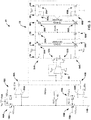
- FIG. 3 is a circuit diagram of a power conversion system 40 including a high-side power switch 44A and a low-side power switch 44B, in accordance with some examples of this disclosure.
- Power switches 44A and 44B may be a part of a half-bridge circuit that operates based on control signals delivered at control terminals 76A and 76B and voltage supplies 74A and 74B.
- the half-bridge circuit may deliver an output current at switch node 42.
- a control terminal of one of power switches 44A and 44B may be electrically connected to a control terminal of one of sensing switches 46A and 46B.
- a load terminal of one of power switches 44A and 44B may be electrically connected to a load terminal of one of sensing switches 46A and 46B.
- sensing switches 46A and 46B may be configured to conduct electrical currents based on the electrical currents conducted by power switches 44A and 44B.
- Power conversion system 40 may also include gate driver circuitry that is configured to deliver control signals at control terminals 76A and 76B to power switches 44A and 44B and to sensing switches 46A and 46B.
- One of operational amplifiers 64A and 64B may drive operational amplifier 50, depending on which of power switches 44A and 44B is active and based on the electrical currents conducted by power switches 44A and 44B and sensing switches 46A and 46B.
- a pulse-width modulated (PWM) signal may control switches 48A and 48B to connect or disconnect operational amplifiers 64A and 64B from an input node of operational amplifier 50.
- the control signals for power switches 44A and 44B received at control terminals 76A and 76B may be PWM signals, pulse-density modulated (PDM) signals, and/or any other suitable waveforms.
- the gate driver circuitry may be configured to control whether trimming circuitry 70 generates a monitored electrical current at the IMON node in FIG. 3 based on the electrical current conducted by sensing switch 46A or 46B by opening and closing switches 48A and 48B to control whether operational amplifier 64A or 64B drives trimming circuitry 70.
- Operational amplifier 50 may be configured to drive branch circuitry 54 of trimming circuitry 70 through transistors 52A and 52B.
- branch circuitry 54 may be configured to be driven by operational amplifier 64A or 64B.
- the source-terminal voltage of high-side sensing switch 46A may be driven by branch circuitries 68, 66, and 60.
- the source-terminal voltage of low-side sensing switch 46B may be driven by branch circuitry 56.
- Branch circuitry 58 may be configured to generate a monitored electrical current at the IMON node in FIG. 3 .
- the monitored electrical current may be based on a ratio between branch circuitry 56 and branch circuitry 58 or based on a ratio between branch circuitry 60 and branch circuitry 58.
- the high-side ratio of trimming circuitry 70 may depend on the number of active transistors configured to conduct electricity in branch circuitries 58 and 60.
- the low-side ratio of trimming circuitry 70 may depend on the number of active transistors configured to conduct electricity in branch circuitries 56 and 58.
- the monitored node of device 40 may be electrically connected to a microcontroller and/or processing circuitry that monitors the monitored electrical current and/or converts the monitored electrical current to a digital value.
- the processing circuitry may be configured to monitor the electrical current generated by trimming circuitry 70.
- the processing circuitry may be configured to control the high-side ratio and/or the low-side ratio of trimming circuitry 70 based on the amplitude of the monitored electrical current.
- FIG. 4 is a circuit diagram of a portion of the trimming circuitry 10 of device 2 in FIGS. 1 and 2 or trimming circuitry 70 of device 40 in FIG. 3 , in accordance with some examples of this disclosure.
- Transistors 90A-90F may be equivalent to one of transistors 56A, 56B, 60A, or 60B.
- Transistors 90A-90F may be n-channel transistors or p-channel transistors. Connected in parallel, transistors 90A-90F may be configured to conduct electricity as a single mirror because the total electrical current through transistors 90A-90F may be the sum of the electrical currents through the active transistors of transistors 90A-90F.
- transistors 90A-90F may connected in parallel because all of source terminals 100A-100F are electrically connected to each other, and all of drain terminals 102A-102F are electrically connected to each other.
- transistors 90A-90F may represent transistor 56A in FIG. 3 .
- Source terminals 100A-100F may be electrically connected to a high-side voltage rail that supplies voltage V DDA .
- the control terminals of transistors 90A-90F may be configured to receive control signals 98, which may also be delivered to the control terminals of transistors 56A and 60A. If transistors 90A-90F are a part of transistor 56A in FIG. 3 , then drain terminals 102A-102F may be electrically connected to a drain terminal of transistor 56B and a source terminal of low-side sensing switch 46B.
- Each of transistors 90A-90F may be configured to conduct electricity in parallel or not conduct electricity in parallel by opening or closing switches 92A-92F.
- signals 96A-96D may close switches 92A-92D
- signals 96E and 96F may open switches 96E and 96F.
- the ratio of branch circuitry 56 or 60 may be based on the number of active transistors 90A-90F that are configured to conduct electricity in parallel.
- the ratio 12 of FIG. 1 for low-side trimming may be four to one if switches 92A-92D are closed and switches 92E and 92F are open.
- One of more of transistors 90A-90F may be configured to conduct electricity in parallel by many other methods.
- the control terminals of transistors 90A-90F may be electrically disconnected from control signals 98 and electrically connected to a respective one of source terminals 100A-100F.
- the control terminal of the respective one of transistors 90A-90F may also be electrically connected to control signals 98 and electrically disconnected from a respective one of source terminals 100A-100F.
- a switch may be placed in series with each of drain terminals 102A-102F to form a cascode circuit with the respective one of transistors 90A-90F.
- the switch of each cascode circuit may be opened or closed to connect or disconnect the respective one of transistors 90A-90F.
- the switch of each cascode circuit may also have its control terminal connected or disconnected from the supply of the current mirror to connect or disconnect the respective one of transistors 90A-90F.
- FIG. 5 is a flowchart illustrating a technique 200 for monitoring an electrical current conducted by a power switch, in accordance with some examples of this disclosure.
- Technique 200 is described with reference to device 2 in FIGS. 1 and 2 , although other components, such as power conversion system 40 in FIG. 3 , may exemplify similar techniques.
- the technique of FIG. 5 includes monitoring electrical current 14 generated by trimming circuitry 10, wherein trimming circuitry 10 is configured to generate monitored electrical current 14 based on aspect ratio 12 of trimming circuitry 10 and based on electrical current 8B conducted by sensing switch 6 (200). Sensing switch 6 is configured to conduct electrical current 8B based on electrical current 8A conducted by power switch 4.
- the monitoring of electrical current 14 may occur during a testing process in the factory and/or in the field. The monitoring may be administered by a technician or a microcontroller may conduct the testing. In some examples, monitored electrical current 14 may be monitored by the microcontroller with an analog-to-digital converter, and electrical current 8A may be monitored by an ammeter connected to device 2.
- the technique of FIG. 5 also includes controlling aspect ratio 12 of trimming circuitry 10 based on monitored electrical current 14 generated by trimming circuitry 10 (202). If the ratio of the measured electrical current 8A and the measured monitored electrical current 14, which may be the KILIS factor, is equal to a target value, then aspect ratio 12 may not need adjustment. If the KILIS factor is not equal to the target value, however, then aspect ratio 12 may be adjusted by controlling the number of active transistors in trimming circuitry 10 configured to conduct electricity in parallel. Referring to trimming circuitry 10 of FIG. 2 , controlling the number of active transistors may include selecting a number of active upper transistors of transistor 30A and selecting a number of active lower transistors of transistor 30B that are configured to conduct electricity in parallel.
- Adding transistors to branch circuitry 30, which may be represented by the variable L may decrease monitored electrical current 14 generated by branch circuitry 32 by decreasing the value of M relative to L.
- the amplitude of monitored electrical current 14 may be based on the number of active transistors connected in parallel in transistors 30A and 30B.
- the KILIS factor may not be equal to the target value. If the actual KILIS factor is lower than the target value, monitored electrical current 14 may be higher than expected when electrical current 8A is at a satisfactory level. As a result, a microcontroller may incorrectly decrease the duty cycle of the control signals delivered to power switch 4 to reduce the electrical power delivered to an electrical load. If the actual KILIS factor is higher than the target value, monitored electrical current 14 may be lower than expected. Even if electrical current 8A is at a satisfactory level, the microcontroller may increase the duty cycle of the control signals delivered to power switch 4. Thus, adjusting aspect ratio 12 may control the KILIS factor closer to the target value, reducing or eliminating the incorrect control of the duty cycle of the control signals delivered to the control terminal of power switch 4.
- FIG. 6 is a circuit diagram of a device 300 configured to regulate a terminal voltage 322 of a sensing switch 306 that is determined based on a reference voltage.
- Device 300 is another possible solution to the problem of reducing the spread of the current ratio between power switch 304 and sensing switch 306.
- Device 300 may include resistor divider 310 positioned between two different points, also known as tapping points, taken on the source metallization of the power switch 304. One tapping point may be source terminal 320 of power switch 304, and the other tapping point may be terminal 318.
- Resistor divider 310 may operate similar to a potentiometer, where the divided voltage is adjustable at the time of production and/or in the field.
- This solution may generate an artificial voltage drop that, divided into steps, provides the trimmed voltage reference used by operational amplifier 324 as one of its inputs.
- the other input of the operational amplifier may be electrically connected to source terminal 322 of the sensing switch 306.
- Sensing switch 306 may be a scaled replica (1 to N) of power switch 304. In this way, the electrical current flowing through sensing switch 306, that should be ideally N times smaller than the electrical current flowing through power switch 304, can be trimmed in order to have exactly the ratio N, although the accuracy depends on the step size decided.
- the current ratio may be dependent on the temperature of device 300. This dependence may be due to the resistance in the source metallization of power switch 304, in parallel with the external resistor, which might be different from that of sensing switch 306. There may be a limited voltage drop achievable in the source metallization of power switch 304 that restricts the trimming capability of device 300. In addition, it may be difficulty to drive the trimming switches in case that mirror circuitry is used in high-side configuration. Lastly, two pads may be necessary for connecting the external resistor.
- sensing switches can be found in U.S. Patent No. 9,152,163, issued October 6, 2015 , and entitled "Regulation of a Load Current-to-Sensing Current Ratio in a Current Sensing Power Metal-Oxide-Semiconductor Field-Effect Transistor (MOSFET)," which is incorporated herein by reference in its entirety.
- MOSFET Current Sensing Power Metal-Oxide-Semiconductor Field-Effect Transistor
Landscapes
- Engineering & Computer Science (AREA)
- Physics & Mathematics (AREA)
- General Physics & Mathematics (AREA)
- Power Engineering (AREA)
- Electromagnetism (AREA)
- Radar, Positioning & Navigation (AREA)
- Automation & Control Theory (AREA)
- Measurement Of Current Or Voltage (AREA)
- Semiconductor Integrated Circuits (AREA)
- Emergency Protection Circuit Devices (AREA)
Abstract
Description
- This disclosure relates to power electronics circuitry.
- A sensing switch may be positioned in parallel with a power switch and configured to mirror the electrical current conducted by the power switch. The ratio of the electrical current conducted by the power switch to the electrical current conducted by the sensing switch may be expressed as N : 1. In some examples, the actual value of N in a device may be different than the target value of N in the device. The ratio of electrical currents may be based on the ratio of the sizes of the two switches.
- This disclosure describes techniques for generating a monitored electrical current that is indicative of the electrical current conducted by a power switch. The techniques of this disclosure include selecting an aspect ratio for trimming circuitry. The trimming circuitry may generate the monitored electrical current based on its aspect ratio and based on the electrical current conducted by the sensing switch. Based on the results of a test of the monitored electrical current, a technician or processing circuitry may select an aspect ratio for the trimming circuitry. Therefore, the monitored electrical current generated by the trimming circuitry may more accurately reflect the target ratio of the electrical current conducted by the power switch to the electrical current conducted by the sensing switch.
- In some examples, a device including a power switch, a sensing switch configured to conduct an electrical current based on an electrical current conducted by the power switch. The device also includes trimming circuitry configured to generate a monitored electrical current based on an aspect ratio of the trimming circuitry and based on the electrical current conducted by the sensing switch, wherein the aspect ratio of the trimming circuitry is adjustable.
- In some examples, a method is for monitoring an electrical current conducted by a power switch, where the method includes monitoring an electrical current generated by trimming circuitry, wherein the trimming circuitry is configured to generate the monitored electrical current based on an aspect ratio of the trimming circuitry and based on an electrical current conducted by a sensing switch, and wherein the sensing switch is configured to conduct the electrical current based on an electrical current conducted by the power switch. The method further includes controlling the aspect ratio of the trimming circuitry based on the monitored electrical current generated by the trimming circuitry.
- In some examples, a power conversion system includes half-bridge circuitry including a high-side power switch and a low-side power switch. The power conversion system further includes a high-side sensing switch configured to conduct an electrical current based on an electrical current conducted by the high-side power switch and a low-side sensing switch configured to conduct an electrical current based on an electrical current conducted by the low-side power switch. The power conversion system also includes trimming circuitry configured to generate a monitored electrical current based on an aspect ratio of the trimming circuitry and based on the electrical current conducted by the high-side sensing switch or the electrical current conducted by the low-side sensing switch, wherein the aspect ratio of the trimming circuitry is adjustable.
- The details of one or more examples are set forth in the accompanying drawings and the description below. Other features, objects, and advantages will be apparent from the description and drawings.
-
FIG. 1 is a conceptual block diagram of a device including trimming circuitry configured to generate a monitored electrical current based on an aspect ratio of the trimming circuitry and the electrical current conducted by a sensing switch, in accordance with some examples of this disclosure. -
FIG. 2 is a circuit diagram of the device ofFIG. 1 , in accordance with some examples of this disclosure. -
FIG. 3 is a circuit diagram of a power conversion system including a high-side power switch and a low-side power switch, in accordance with some examples of this disclosure. -
FIG. 4 is a circuit diagram of a portion of the trimming circuitry of the devices of any ofFIGS. 1-3 , in accordance with some examples of this disclosure. -
FIG. 5 is a flowchart illustrating a technique for monitoring an electrical current conducted by a power switch, in accordance with some examples of this disclosure. -
FIG. 6 is a circuit diagram of a device configured to regulate a terminal voltage of a sensing switch that is determined based on a reference voltage. - The techniques of this disclosure may improve power electronics by reducing the spread of the ratio between the electrical current conducted by a power switch and a monitored electrical current generated by trimming circuitry. In some examples, a device of this disclosure may include one or more monolithic mirror structures. The ratio between the power switch electrical current and the monitored electrical current may be adjustable by several methods and/or configurations. By adjusting the current ratio, a device of this disclosure may generate a more reliable monitored electrical current, which may allow more accurate monitoring of the power switch electrical current, along with lower power dissipation.
- A device of this disclosure may move the trimming operation from the power switch to front-end circuitry such as trimming circuitry. In this way, the trimming of the current ratio may not be limited by the voltage drop of the metallization on the power switch, which may possibly increase the trimming range. The temperature of the device may have a relatively small effect on the operation of the trimming circuitry because it employs a single "tapping point" which makes the trimming circuitry, ideally, temperature independent. Other arrangements including more than one tapping point may, in some examples, depend on the temperature of the components. It may also be possible to trim the high-side current ratio and to match it to the low-side current ratio, for applications that include a half bridge circuit. Moreover, the device may need only one tapping point contacting the source of the power switch, reducing the number of pads in the device.
- Other methods for adjusting a monitored electrical current may include complicated circuitry that takes up more space on a semiconductor die, as compared to the operational amplifiers and trimming circuitry of this disclosure. Other methods may also have greater dependence on temperature than the methods of this disclosure. Thus, in some examples, the techniques of this disclosure may allow for smaller and more accurate devices.
- A device of this disclosure may have several unique ratios between devices and circuits. The "aspect ratio" of the trimming circuitry may be defined as the ratio of the number of active transistors in one branch of the trimming circuitry to the number of active transistors in another branch of the trimming circuitry. The "aspect ratio" may also be defined as the ratio of the electrical current through one branch of the trimming circuitry to the electrical current through another branch of the trimming circuitry. The "aspect ratio" of the trimming circuitry may be represented herein as L : M or M : L, where L is the number of active transistors in one branch and M is the number of active transistors in another branch. In some examples, the trimming circuitry may include more than two branches, and one of the branches may include a single active transistor. The ratio of the single-transistor branch to the other branches may be represented as 1 : L and 1 : M. The ratios of 1 : L and 1 : M are not referred to as aspect ratios herein.
- A device of this disclosure may also include a ratio of the power switch to the sensing switch, which may be represented as N : 1, where the power switch is N times larger than the sensing switch and/or include N times more modules or cells than the sensing switch. The electrical current conducted by the power switch may also be N times larger than the electrical current conducted by the sensing switch. This disclosure may not refer to the ratio of N : 1 as an aspect ratio.
-
FIG. 1 is a conceptual block diagram of adevice 2 includingtrimming circuitry 10 configured to generate a monitoredelectrical current 14 based on an aspect ratio 12 of thetrimming circuitry 10 and theelectrical current 8B conducted by asensing switch 6, in accordance with some examples of this disclosure.Device 2 includespower switch 4,sensing switch 6, and trimmingcircuitry 10.Device 2 may be a power electronics device, an analog electrical device, an embedded system, an integrated circuit (IC) device, a power conversion device, a motor driver circuit, and/or any other electrical device. In some examples,device 2 may be a single integrated semiconductor die or more than one semiconductor die.Device 2 may be configured to deliverelectrical current 8A to an electrical load. The electrical load connected to a switch node that is electrically connected topower switch 4. - In some examples,
device 2 may be a power conversion device, such as an alternating-current-to-direct-current (AC/DC) converter, an AC/AC converter, or a DC/DC converter.Device 2 may include two power switches arranged as a half-bridge circuit and configured to generate an output signal at a switch node that is positioned between the two power switches. In some examples,device 2 may be a multiphase power converter and may include two or more half-bridge circuits or two or more H-bridge circuits. Each power switch ofdevice 2 may include a sensing switch that includes one or more modules ofdevice 2, wheredevice 2 may include numerous modules (i.e., cells or transistors) and each power switch includes two or more modules connected in parallel. In some examples,device 2 may operate as a buck converter, a boost converter, a buck-boost converter, a flyback converter, a resonant mode converter such as an LLC converter, and/or a multiphase power converter. -
Power switch 4 is configured to conductelectrical current 8A.Electrical current 8A may flow from a first load terminal ofpower switch 4 to a second load terminal ofpower switch 4 based on the voltage at a control terminal ofpower switch 4. Based on the voltage at the control terminal ofpower switch 4,power switch 4 may turn on and off.Power switch 4 may be configured to receive electrical power from a power source, modify it, and deliver the electrical power to an electrical load. The electrical power transmitted bypower switch 4 may also depend on the duty cycle of the control signals received bypower switch 4.Power switch 4 and/orsensing switch 6 may include, but are not limited to, any type of field-effect transistor (FET), a bipolar junction transistor (BJT), an insulated-gate bipolar transistor (IGBT), a high-electron-mobility transistor (HEMT) such as a gallium-nitride (GaN) based transistor or a silicon carbide (SiC) transistor, or another element that uses voltage for its control. -
Power switch 4 and/orsensing switch 6 may include various material compounds, such as silicon (Si), silicon carbide (SiC), Gallium Nitride (GaN), or any other combination of one or more semiconductor materials. To take advantage of higher power density requirements in some circuits, power converters may operate at higher frequencies. In some examples, SiC switches may experience lower switching power losses. Improvements in magnetics and faster switching, such as GaN and SiC switches, may support higher frequency converters. These higher frequency circuits may require control signals to be sent with more precise timing, as compared to lower-frequency circuits. - In some examples,
power switch 4 may include two or more cells or modules connected in parallel. Each of the cells or modules ofpower switch 4 may be a transistor with two load terminals and a control terminal.Sensing switch 6 may include one or more cells. In some examples, the drain terminals of the cells ofpower switch 4 and the cells ofsensing switch 6 may be electrically connected, and the gate terminals of the cells ofpower switch 4 and the cells ofsensing switch 6 may be electrically connected. The source terminals of the cells ofpower switch 4 may be electrically connected to a switch node ofdevice 2, while the source terminals of the cells ofsensing switch 6 may be electrically connected to trimmingcircuitry 10. Thus,power switch 4 andsensing switch 6 may be a part of the same semiconductor die, even though a load terminal (e.g., a source terminal) ofsensing switch 6 may be electrically disconnected from a load terminal (e.g., a source terminal) ofpower switch 4. -
Sensing switch 6 is configured to conduct electrical current 8B based on electrical current 8A. The ratio ofelectrical currents electrical currents power switch 4 andsensing switch 6. In some examples, the ratio N may be one thousand, ten thousand, or thirty thousand, where electrical current 8A is N times larger than electrical current 8B. In some examples, a load terminal ofpower switch 4 may be electrically connected to a load terminal ofsensing switch 6, and a control terminal ofpower switch 4 may be electrically connected to a control terminal ofsensing switch 6. In some examples, switches 4 and 6 may have a common control terminal (e.g., gate terminal) and a common load terminal (e.g., drain terminal). Thus,power switch 4 andsensing switch 6 may be configured to conductelectrical currents - According to the techniques described herein, trimming
circuitry 10 can be configured to generate monitored electrical current 14 based on aspect ratio 12 and based on electrical current 8B. Aspect ratio 12 may be based on a number of active transistors in trimmingcircuitry 10 that are configured to conduct electricity in parallel. The transistors of trimmingcircuitry 10 may also be called modules, as explained in the description ofFIG. 4 . Trimmingcircuitry 10 may include two or more branch circuits, where one of the branch circuits may be configured to generate monitored electrical current 14. In some examples, trimmingcircuitry 10 may include current mirror circuitry, where one or more branch circuit of trimmingcircuitry 10 may be configured to conduct an electrical current based on the electrical current of another branch circuitry. Aspect ratio 12 may represent the ratio of electrical currents in two different branch circuits of trimmingcircuitry 10. Aspect ratio 12 may also be based on the combined width-to-length ratios of the transistors and/or based on the on-resistances of the transistors. - In some examples, trimming
circuitry 10 may be configured to trim electrical current 8B in order to generate monitored electrical current 14 at a lower amplitude than electrical current 8B. The lower amplitude of monitored electrical current 14 may result in lower power consumption ofdevice 2. Electrical current 8B may be trimmed to generate monitored electrical current 14 based on aspect ratio 12, which may be adjustable. In some examples, the aspect ratio of each figure of this disclosure may be defined the same or differently. For example,FIG. 2 depicts only one aspect ratio in trimmingcircuitry 10, whileFIG. 3 depicts a high-side aspect ratio and a low-side aspect ratio in trimmingcircuitry 70. - Monitored electrical current 14 may flow through a resistor. A microcontroller and/or processing circuitry may monitor the voltage drop across the resistor caused by monitored electrical current 14. In some examples, the microcontroller may convert the voltage drop to a digital value. The microcontroller may use the digital value to determine if electrical current 8A is too high or too low. The microcontroller may adjust the duty cycle of the control signals delivered to the control terminal of
power switch 4 to adjust the amplitude of electrical current 8A.Device 2 may generate monitored electrical current 14 at a lower amplitude in order to reduce the power dissipation caused by monitored electrical current 14. - In accordance with the techniques of this disclosure, aspect ratio 12 can be adjustable. By adjusting aspect ratio 12, the amplitude of monitored electrical current 14 may be adjusted to a desired level. During the operation of
device 2, processing circuitry may monitor the level of monitored electrical current 14 to determine the amplitude of electrical current 8A. Determining the amplitude of electrical current 8A may be desirable becausedevice 2 may deliver electrical current 8A to an electrical load. - In some examples, the designers of
device 2 may choose the ratio betweenelectrical currents device 2, N may be equal to the target value or may be different than the target value. If N is different than the target value, a KILIS factor may be adjusted closer to the target value by adjusting the number of active transistors configured to conduct electricity in parallel in trimmingcircuitry 10. In some examples, trimmingcircuitry 10 may include passive elements such as resistors, capacitors, or inductors, and aspect ratio 12 may be adjusted by adjusting, connecting, and/or disconnecting the passive elements. In some examples, aspect ratio 12 may be adjustable by controlling transistors and/or passive elements. Additionally or alternatively, aspect ratio 12 may also be adjustable by any other suitable means that adjusts the current ratio or a current mirror in trimmingcircuitry 10 in order to trim monitored electrical current 14 to a desirable amplitude. - The KILIS factor may represent the actual ratio of electrical current 8A to electrical current 8B, where N is the ratio of electrical current 8A to electrical current 8B before adjustment. Adjusting, or trimming, the KILIS factor may result in trimming or modifying monitored electrical current 14, such that monitored electrical current 14 is a more accurate representation of electrical current 8A. The KILIS factor, which is explained further below, may be based on aspect ratio 12, such that adjustment of the aspect ratio 12 may result in adjustment of the KILIS factor.
-
FIG. 2 is a circuit diagram of the device ofFIG. 1 , in accordance with some examples of this disclosure.Device 2 may includepower switch 4,sensing switch 6, trimmingcircuitry 10,operational amplifier 24, and monitorednode 38. Trimmingcircuitry 10 may includetransistors branch circuitries channel transistors channel transistors - In some examples, aspect ratio 12 of
FIG. 2 may be based on the ratio between the number of active transistors inbranch circuitry 30 and the number of active transistors inbranch circuitry 32. If each oftransistors branch circuitries transistors circuitry 10 may also include inactive transistors that are not configured to conduct electricity in parallel. The aspect ratio ofbranch circuitries transistors FIG. 2 may be equal to the ratio of L to M or M to L. Aspect ratio 12 may also be based on the sizes and other characteristics of the transistors inbranch circuitry device 2 may include a high-side aspect ratio and a low-side aspect ratio, where the high-side aspect ratio may be equal to or different than the low-side aspect ratio. -
Operational amplifier 24 may be configured to drivebranch circuitry 28 based onelectrical currents Operational amplifier 24 may be configured to receive source-terminal voltages electrical currents transistors Branch circuitry 30 may be configured to be driven by electrical current 8B and source-terminal voltage 22.Branch circuitry 32 may be configured to generate monitored electrical current 14 based on aspect ratio 12 betweenbranch circuitries - Each of
branch circuitries upper transistors lower transistors FIG. 2 depicts the upper transistors ofbranch circuitry 30 astransistor 30A, but there may be more than one upper transistor configured to conduct electricity in parallel inbranch circuitry 30. Aspect ratio 12 may be adjustable by selecting the number of active transistors configured to conduct electricity inbranch circuitry 30. The amplitude of monitored electrical current 14 may be based on the number of active upper transistors connected in parallel inbranch circuitry 30 and based on the number of active lower transistors connected in parallel inbranch circuitry 30. The amplitude of monitored electrical current 14 may be based on the number of active transistors connected in parallel inbranch circuitry 32, but the number of active transistors connected in parallel inbranch circuitry 32 may not be adjustable in some examples. -
Device 2 provides a degree of freedom and the opportunity to trim any offset current on monitored electrical current 14 when electrical current 8A is equal to zero, i.e., no current is flowing throughpower switch 4. This can be achieved by trimming separately the p-channel mirrors and the n-channel mirrors present in the output branch of the loop, i.e., trimmingcircuitry 10. The p-channel mirrors may includetransistors transistors Device 2 can work with positive and negative amplitudes of electrical current 8A. -
Device 2 includespower switch 4 andsensing switch 6, wherepower switch 4 may be N times larger than sensingswitch 6.Device 2 also comprises a current reading front-end that reads a suitable potential over the source metallization ofpower switch 4 and forces the potential on the source terminal ofsensing switch 6. The current reading front-end usesoperational amplifier 24 driving p-channel mirrors and n-channel mirrors in trimmingcircuitry 10. The current mirrors inbranch circuitry 30, of multiplicity or ratio L, are within the regulation loop and supply the current flowing throughsensing switch 6. In some examples, the ratio L may be the ratio of transistors inbranch circuitry - The addition of
branch circuitry 32 of transistors of multiplicity M, matched to those of ratio L but lying outside the linear loop, provides the current sensing information at monitorednode 38. The trimming of the KILIS factor is achieved by modifying the ratio L with respect to the ratio M, for example by adding or subtracting transistors (i.e., modules) to the upper transistors and the lower transistors inbranch circuitry 30. - The trimming operation is done completely at the front-end circuit (i.e., a driver integrated circuit), which is trimming
circuitry 10. Therefore, other trimming solutions, which may rely heavily on characteristics ofpower switch 4, may be avoided.Device 2 allows easy trimming or adjusting high-side KILIS factor and low-side KILIS factor to match the KILIS factors to the same value. The KILIS factor is explained in detail below and may be equal to the actual ratio ofelectrical currents - Moreover, the system allows trimming of any offset current in monitored electrical current 14 by modifying separately the p-channel mirrors and the n-channel mirrors present in
branch circuitry 30 of the loop. The target of the trimming is to obtain the maximum accuracy in the amplitude of monitored electrical current 14 by compensating the process spread of the geometrical ratio N, which may or may not be equal to the target value afterdevice 2 is manufactured. -
Device 2 may include a KILIS factor, which is a parameter characterizing the current sensing system and defined by equation (1). The KILIS factor may represent electrical current 8A (ILOAD) divided by electrical current 8B (ISENSE). In some examples, ILOAD may be an electrical current conducted through a switch node of a half-bridge circuit includingpower switch 4 and another power switch.
- Equation (1) may be rewritten as equation (2) based on the relationship between electrical current 8A and monitored electrical current 14. This relationship may be based on ratio L of
branch circuitry 28 andbranch circuitry 30. The relationship may be based on ratio M ofbranch circuitry 28 andbranch circuitry 32. In some examples, the ratio of L divided by M, or M divided by L, may be equal to aspect ratio 12 ofFIG. 2 .
- KILIS is a system parameter, and it may be necessary to know its default value. Therefore, in the absence of trimming, it may be useful to have known default values of L and M (LDEF and MDEF). Based on these values, equation (2) may be rewritten as equation (3):

- LDEF and MDEF may be constants such as, for example, LDEF equals five and MDEF equals one. As shown in
FIG. 2 , the proposed trimming technique varies ratio L of the modules and/or transistors within the regulation loop while keeping constant ratio M of the modules and/or transistors out of the loop. In other words, L can be modified and M may have a constant value ideally equal to MDEF, but in practice this quantity may be subject to the mismatch between the modules forming L and the modules forming M. Monitored electrical current 14 is, therefore, given by the following expression:
- Ratio N may be equal to electrical current 8A divided by electrical current 8B. Where it was assumed that ILOAD equals electrical current 8A and hence the matching between
power switch 4 and sensing current 6 was exploited. Replacing equation (4) into equation (3) yields:
- Equation (5) shows that the KILIS factor is a linear function of ratio L of the modules and/or transistors. Therefore, ratio L may be used for compensating the process spread of the geometrical ratio N without acting on
power switch 4. Moreover, L can be used for compensating mismatch errors which make M different from MDEF or which make the default value of L different from LDEF. In the absence of trimming and under the assumption that there are no mismatch errors, L equals LDEF, M equals MDEF and therefore KILIS equals N. In general, the parameter L may be adjusted to the value that satisfies the following relationship:
-
FIG. 3 is a circuit diagram of apower conversion system 40 including a high-side power switch 44A and a low-side power switch 44B, in accordance with some examples of this disclosure. Power switches 44A and 44B may be a part of a half-bridge circuit that operates based on control signals delivered atcontrol terminals voltage supplies switch node 42. - At each of
control terminals power switches sensing switches nodes power switches sensing switches sensing switches power switches 44A and 44B.Power conversion system 40 may also include gate driver circuitry that is configured to deliver control signals atcontrol terminals power switches sensing switches - One of
operational amplifiers operational amplifier 50, depending on which ofpower switches power switches sensing switches switches operational amplifiers operational amplifier 50. In some examples, the control signals forpower switches control terminals circuitry 70 generates a monitored electrical current at the IMON node inFIG. 3 based on the electrical current conducted by sensingswitch closing switches operational amplifier drives trimming circuitry 70. -
Operational amplifier 50 may be configured to drivebranch circuitry 54 of trimmingcircuitry 70 throughtransistors branch circuitry 54 may be configured to be driven byoperational amplifier side sensing switch 46A may be driven bybranch circuitries side sensing switch 46B may be driven bybranch circuitry 56.Branch circuitry 58 may be configured to generate a monitored electrical current at the IMON node inFIG. 3 . - The monitored electrical current may be based on a ratio between
branch circuitry 56 andbranch circuitry 58 or based on a ratio betweenbranch circuitry 60 andbranch circuitry 58. The high-side ratio of trimmingcircuitry 70 may depend on the number of active transistors configured to conduct electricity inbranch circuitries circuitry 70 may depend on the number of active transistors configured to conduct electricity inbranch circuitries - The monitored node of
device 40 may be electrically connected to a microcontroller and/or processing circuitry that monitors the monitored electrical current and/or converts the monitored electrical current to a digital value. The processing circuitry may be configured to monitor the electrical current generated by trimmingcircuitry 70. The processing circuitry may be configured to control the high-side ratio and/or the low-side ratio of trimmingcircuitry 70 based on the amplitude of the monitored electrical current. -
FIG. 4 is a circuit diagram of a portion of the trimmingcircuitry 10 ofdevice 2 inFIGS. 1 and2 or trimmingcircuitry 70 ofdevice 40 inFIG. 3 , in accordance with some examples of this disclosure.Transistors 90A-90F may be equivalent to one oftransistors Transistors 90A-90F may be n-channel transistors or p-channel transistors. Connected in parallel,transistors 90A-90F may be configured to conduct electricity as a single mirror because the total electrical current throughtransistors 90A-90F may be the sum of the electrical currents through the active transistors oftransistors 90A-90F. In some examples,transistors 90A-90F may connected in parallel because all ofsource terminals 100A-100F are electrically connected to each other, and all ofdrain terminals 102A-102F are electrically connected to each other. - For example,
transistors 90A-90F may representtransistor 56A inFIG. 3 .Source terminals 100A-100F may be electrically connected to a high-side voltage rail that supplies voltage VDDA. The control terminals oftransistors 90A-90F may be configured to receivecontrol signals 98, which may also be delivered to the control terminals oftransistors transistors 90A-90F are a part oftransistor 56A inFIG. 3 , then drainterminals 102A-102F may be electrically connected to a drain terminal oftransistor 56B and a source terminal of low-side sensing switch 46B. - Each of
transistors 90A-90F may be configured to conduct electricity in parallel or not conduct electricity in parallel by opening or closing switches 92A-92F. For example, to cause four oftransistors 90A-90F to conduct electricity in parallel, signals 96A-96D may closeswitches 92A-92D, and signals 96E and 96F may openswitches branch circuitry active transistors 90A-90F that are configured to conduct electricity in parallel. Thus, the ratio 12 ofFIG. 1 for low-side trimming may be four to one ifswitches 92A-92D are closed andswitches - One of more of
transistors 90A-90F may be configured to conduct electricity in parallel by many other methods. In some examples, the control terminals oftransistors 90A-90F may be electrically disconnected fromcontrol signals 98 and electrically connected to a respective one ofsource terminals 100A-100F. To reconnect a transistor, the control terminal of the respective one oftransistors 90A-90F may also be electrically connected to controlsignals 98 and electrically disconnected from a respective one ofsource terminals 100A-100F. Alternatively or additionally, a switch may be placed in series with each ofdrain terminals 102A-102F to form a cascode circuit with the respective one oftransistors 90A-90F. The switch of each cascode circuit may be opened or closed to connect or disconnect the respective one oftransistors 90A-90F. The switch of each cascode circuit may also have its control terminal connected or disconnected from the supply of the current mirror to connect or disconnect the respective one oftransistors 90A-90F. -
FIG. 5 is a flowchart illustrating atechnique 200 for monitoring an electrical current conducted by a power switch, in accordance with some examples of this disclosure.Technique 200 is described with reference todevice 2 inFIGS. 1 and2 , although other components, such aspower conversion system 40 inFIG. 3 , may exemplify similar techniques. - The technique of
FIG. 5 includes monitoring electrical current 14 generated by trimmingcircuitry 10, wherein trimmingcircuitry 10 is configured to generate monitored electrical current 14 based on aspect ratio 12 of trimmingcircuitry 10 and based on electrical current 8B conducted by sensing switch 6 (200).Sensing switch 6 is configured to conduct electrical current 8B based on electrical current 8A conducted bypower switch 4. The monitoring of electrical current 14 may occur during a testing process in the factory and/or in the field. The monitoring may be administered by a technician or a microcontroller may conduct the testing. In some examples, monitored electrical current 14 may be monitored by the microcontroller with an analog-to-digital converter, and electrical current 8A may be monitored by an ammeter connected todevice 2. - The technique of
FIG. 5 also includes controlling aspect ratio 12 of trimmingcircuitry 10 based on monitored electrical current 14 generated by trimming circuitry 10 (202). If the ratio of the measured electrical current 8A and the measured monitored electrical current 14, which may be the KILIS factor, is equal to a target value, then aspect ratio 12 may not need adjustment. If the KILIS factor is not equal to the target value, however, then aspect ratio 12 may be adjusted by controlling the number of active transistors in trimmingcircuitry 10 configured to conduct electricity in parallel. Referring to trimmingcircuitry 10 ofFIG. 2 , controlling the number of active transistors may include selecting a number of active upper transistors oftransistor 30A and selecting a number of active lower transistors oftransistor 30B that are configured to conduct electricity in parallel. Adding transistors tobranch circuitry 30, which may be represented by the variable L, may decrease monitored electrical current 14 generated bybranch circuitry 32 by decreasing the value of M relative to L. Thus, the amplitude of monitored electrical current 14 may be based on the number of active transistors connected in parallel intransistors - Without trimming, adjusting, or selecting aspect ratio 12, the KILIS factor may not be equal to the target value. If the actual KILIS factor is lower than the target value, monitored electrical current 14 may be higher than expected when electrical current 8A is at a satisfactory level. As a result, a microcontroller may incorrectly decrease the duty cycle of the control signals delivered to
power switch 4 to reduce the electrical power delivered to an electrical load. If the actual KILIS factor is higher than the target value, monitored electrical current 14 may be lower than expected. Even if electrical current 8A is at a satisfactory level, the microcontroller may increase the duty cycle of the control signals delivered topower switch 4. Thus, adjusting aspect ratio 12 may control the KILIS factor closer to the target value, reducing or eliminating the incorrect control of the duty cycle of the control signals delivered to the control terminal ofpower switch 4. -
FIG. 6 is a circuit diagram of adevice 300 configured to regulate aterminal voltage 322 of asensing switch 306 that is determined based on a reference voltage.Device 300 is another possible solution to the problem of reducing the spread of the current ratio betweenpower switch 304 andsensing switch 306.Device 300 may includeresistor divider 310 positioned between two different points, also known as tapping points, taken on the source metallization of thepower switch 304. One tapping point may besource terminal 320 ofpower switch 304, and the other tapping point may be terminal 318.Resistor divider 310 may operate similar to a potentiometer, where the divided voltage is adjustable at the time of production and/or in the field. - This solution may generate an artificial voltage drop that, divided into steps, provides the trimmed voltage reference used by
operational amplifier 324 as one of its inputs. The other input of the operational amplifier may be electrically connected to source terminal 322 of thesensing switch 306.Sensing switch 306 may be a scaled replica (1 to N) ofpower switch 304. In this way, the electrical current flowing throughsensing switch 306, that should be ideally N times smaller than the electrical current flowing throughpower switch 304, can be trimmed in order to have exactly the ratio N, although the accuracy depends on the step size decided. - The current ratio may be dependent on the temperature of
device 300. This dependence may be due to the resistance in the source metallization ofpower switch 304, in parallel with the external resistor, which might be different from that ofsensing switch 306. There may be a limited voltage drop achievable in the source metallization ofpower switch 304 that restricts the trimming capability ofdevice 300. In addition, it may be difficulty to drive the trimming switches in case that mirror circuitry is used in high-side configuration. Lastly, two pads may be necessary for connecting the external resistor. - Further example details of sensing switches can be found in
U.S. Patent No. 9,152,163, issued October 6, 2015 - The following numbered examples demonstrate one or more aspects of the disclosure.
- Example 1. A device includes a power switch, a sensing switch configured to conduct an electrical current based on an electrical current conducted by the power switch. The device also includes trimming circuitry configured to generate a monitored electrical current based on an aspect ratio of the trimming circuitry and based on the electrical current conducted by the sensing switch, wherein the aspect ratio of the trimming circuitry is adjustable.
- Example 2. The device of example 1, wherein the aspect ratio of the trimming circuitry is based on a number of active transistors that are configured to conduct electricity in parallel, and wherein the number of active transistors is adjustable.
- Example 3. The device of examples 1-2 or any combination thereof, further including an operational amplifier configured to drive the trimming circuitry based on the electrical current conducted by the power switch and the electrical current conducted by the sensing switch.
- Example 4. The device of examples 1-3 or any combination thereof, wherein the trimming circuitry includes first branch circuitry configured to be driven by the operational amplifier and second branch circuitry configured to be driven by the electrical current conducted by the sensing switch. The trimming circuitry also includes third branch circuitry configured to generate the monitored electrical current based on an aspect ratio between the second branch circuitry and the third branch circuitry.
- Example 5. The device of examples 1-4 or any combination thereof, wherein the second branch circuitry includes a number of active upper transistors and a number of active lower transistors, wherein the number of active lower transistors is adjustable, and wherein the number of active upper transistors is adjustable.
- Example 6. The device of examples 1-5 or any combination thereof, wherein the aspect ratio between the second branch circuitry and the third branch circuitry is adjustable by at least selecting the number of active upper transistors configured to conduct electricity in the second branch circuitry and selecting the number of active lower transistors configured to conduct electricity in the second branch circuitry.
- Example 7. The device of examples 1-6 or any combination thereof, wherein an amplitude of the monitored electrical current is based on the number of active upper transistors connected in parallel in the second branch circuitry and based on the number of active lower transistors connected in parallel in the second branch circuitry.
- Example 8. The device of examples 1-7 or any combination thereof, wherein a first input node of the operational amplifier is electrically connected to a load terminal of the power switch, and wherein a second input node of the operational amplifier is electrically connected to a load terminal of the sensing switch.
- Example 9. A method for monitoring an electrical current conducted by a power switch, where the method includes monitoring an electrical current generated by trimming circuitry, wherein the trimming circuitry is configured to generate the monitored electrical current based on an aspect ratio of the trimming circuitry and based on an electrical current conducted by a sensing switch, and wherein the sensing switch is configured to conduct the electrical current based on an electrical current conducted by the power switch. The method further includes controlling the aspect ratio of the trimming circuitry based on the monitored electrical current generated by the trimming circuitry.
- Example 10. The method of example 9, wherein controlling the aspect ratio of the trimming circuitry includes controlling a number of active transistors in the trimming circuitry that are configured to conduct electricity in parallel.
- Example 11. The method of examples 9-10 or any combination thereof, wherein first branch circuitry of the trimming circuitry is configured to be driven by the electrical current conducted by the sensing switch, wherein second branch circuitry of the trimming circuitry is configured to generate the monitored electrical current based on an aspect ratio between the first branch circuitry and the second branch circuitry, and wherein controlling the aspect ratio of the trimming circuitry includes controlling the aspect ratio between first branch circuitry and second branch circuitry.
- Example 12. The method of examples 9-11 or any combination thereof, wherein the first branch circuitry includes a number of active upper transistors and a number of active lower transistors, and wherein controlling the aspect ratio between first branch circuitry and second branch circuitry includes selecting the number of active upper transistors in the first branch circuitry and selecting the number of active lower transistors in the first branch circuitry.
- Example 13. The method of examples 9-12 or any combination thereof, wherein an amplitude of the monitored electrical current is based on the number of active upper transistors connected in parallel in the first branch circuitry and based on the number of active lower transistors connected in parallel in the first branch circuitry.
- Example 14. A power conversion system includes half-bridge circuitry including a high-side power switch and a low-side power switch. The power conversion system further includes a high-side sensing switch configured to conduct an electrical current based on an electrical current conducted by the high-side power switch and a low-side sensing switch configured to conduct an electrical current based on an electrical current conducted by the low-side power switch. The power conversion system also includes trimming circuitry configured to generate a monitored electrical current based on an aspect ratio of the trimming circuitry and based on the electrical current conducted by the high-side sensing switch or the electrical current conducted by the low-side sensing switch, wherein the aspect ratio of the trimming circuitry is adjustable.
- Example 15. The power conversion system of example 14, wherein the aspect ratio of the trimming circuitry is based on a number of active transistors that are configured to conduct electricity in parallel, and wherein the number of active transistors is adjustable.
- Example 16. The power conversion system of examples 14-15 or any combination thereof, further including gate driver circuitry configured to deliver high-side control signals to the high-side power switch and the high-side sensing switch, deliver low-side control signals to the low-side power switch and the low-side sensing switch, and control whether the trimming circuitry generates the monitored electrical current based on the electrical current conducted by the high-side sensing switch or based on the electrical current conducted by the low-side sensing switch.
- Example 17. The power conversion system of examples 14-16 or any combination thereof, further including a high-side operational amplifier configured to drive the trimming circuitry based on the electrical current conducted by the high-side power switch and the electrical current conducted by the high-side sensing switch. The power conversion system also includes a low-side operational amplifier configured to drive the trimming circuitry based on the electrical current conducted by the low-side power switch and the electrical current conducted by the low-side sensing switch. The gate driver circuitry is configured to control whether the trimming circuitry generates the monitored electrical current based on the electrical current conducted by the high-side sensing switch or based on the electrical current conducted by the low-side sensing switch by at least controlling whether the high-side operational amplifier drives the trimming circuitry and controlling whether the low-side operational amplifier drives the trimming circuitry.
- Example 18. The power conversion system of examples 14-17 or any combination thereof, wherein the trimming circuitry includes first branch circuitry configured to be driven by the high-side operational amplifier or the low-side operational amplifier. The trimming circuitry also includes second branch circuitry configured to be driven by the electrical current conducted by the high-side sensing switch. The trimming circuitry includes third branch circuitry configured to be driven by the electrical current conducted by the low-side sensing switch. The trimming circuitry further includes fourth branch circuitry configured to generate the monitored electrical current based on an aspect ratio between the second branch circuitry and the fourth branch circuitry or based on an aspect ratio between the third branch circuitry and the fourth branch circuitry.
- Example 19. The power conversion system of examples 14-18 or any combination thereof, wherein the aspect ratio between the second branch circuitry and the fourth branch circuitry is adjustable by selecting a number of active transistors connected in parallel in the second branch circuitry. The aspect ratio between the third branch circuitry and the fourth branch circuitry is adjustable by selecting a number of active transistors connected in parallel in the third branch circuitry.
- Example 20. The power conversion system of examples 14-19 or any combination thereof, further including processing circuitry configured to measure the monitored electrical current generated by the trimming circuitry. The processing circuitry is configured to control the aspect ratio of the trimming circuitry based on an amplitude of the monitored electrical current.
- Example 21. The device of examples 1-8 or any combination thereof, wherein the aspect ratio of the trimming circuitry is based on characteristics of passive elements of the trimming circuitry.
- Example 22. The device of examples 1-8 and 21 or any combination thereof, wherein the trimming circuitry includes current mirror circuitry, and wherein the aspect ratio of the trimming circuitry includes an aspect ratio of the current mirror circuitry.
- Various examples of the disclosure have been described. Any combination of the described systems, operations, or functions is contemplated.
Claims (15)
- A device comprising:a power switch;a sensing switch configured to conduct an electrical current based on an electrical current conducted by the power switch; andtrimming circuitry configured to generate a monitored electrical current based on an aspect ratio of the trimming circuitry and based on the electrical current conducted by the sensing switch, wherein the aspect ratio of the trimming circuitry is adjustable.
- The device of claim 1, wherein the aspect ratio of the trimming circuitry is based on a number of active transistors that are configured to conduct electricity in parallel, and wherein the number of active transistors is adjustable.
- The device of claim 1 or 2, further comprising an operational amplifier configured to drive the trimming circuitry based on the electrical current conducted by the power switch and the electrical current conducted by the sensing switch.
- The device of claim 3, wherein the trimming circuitry includes:first branch circuitry configured to be driven by the operational amplifier;second branch circuitry configured to be driven by the electrical current conducted by the sensing switch; andthird branch circuitry configured to generate the monitored electrical current based on an aspect ratio between the second branch circuitry and the third branch circuitry.
- The device of claim 4, wherein the second branch circuitry includes a number of active upper transistors and a number of active lower transistors, wherein the number of active lower transistors is adjustable, and wherein the number of active upper transistors is adjustable.
- The device of claim 5, wherein the aspect ratio between the second branch circuitry and the third branch circuitry is adjustable by at least:selecting the number of active upper transistors configured to conduct electricity in the second branch circuitry; andselecting the number of active lower transistors configured to conduct electricity in the second branch circuitry.
- The device of claim 6, wherein an amplitude of the monitored electrical current is based on the number of active upper transistors connected in parallel in the second branch circuitry and based on the number of active lower transistors connected in parallel in the second branch circuitry.
- The device of any one of claims 3 to 7, wherein a first input node of the operational amplifier is electrically connected to a load terminal of the power switch, and wherein a second input node of the operational amplifier is electrically connected to a load terminal of the sensing switch.
- The device of any one of the preceding claims, wherein the aspect ratio of the trimming circuitry is based on characteristics of passive elements of the trimming circuitry.
- The device of any one of the preceding claims, wherein the trimming circuitry includes current mirror circuitry, and wherein the aspect ratio of the trimming circuitry includes an aspect ratio of the current mirror circuitry.
- A method for monitoring an electrical current conducted by a power switch, the method comprising:monitoring an electrical current generated by trimming circuitry, wherein the trimming circuitry is configured to generate the monitored electrical current based on an aspect ratio of the trimming circuitry and based on an electrical current conducted by a sensing switch, wherein the sensing switch is configured to conduct the electrical current based on an electrical current conducted by the power switch; andcontrolling the aspect ratio of the trimming circuitry based on the monitored electrical current generated by the trimming circuitry.
- The method of claim 11, wherein controlling the aspect ratio of the trimming circuitry comprises controlling a number of active transistors in the trimming circuitry that are configured to conduct electricity in parallel.
- The method of claim 11 or 12,
wherein first branch circuitry of the trimming circuitry is configured to be driven by the electrical current conducted by the sensing switch;
wherein second branch circuitry of the trimming circuitry is configured to generate the monitored electrical current based on an aspect ratio between the first branch circuitry and the second branch circuitry; and
wherein the first branch circuitry includes a number of active upper transistors and a number of active lower transistors, the method further comprising:selecting the number of active upper transistors in the first branch circuitry; andselecting the number of active lower transistors in the first branch circuitry. - A power conversion system comprising:half-bridge circuitry including a high-side power switch and a low-side power switch;a high-side sensing switch configured to conduct an electrical current based on an electrical current conducted by the high-side power switch;a low-side sensing switch configured to conduct an electrical current based on an electrical current conducted by the low-side power switch; andtrimming circuitry configured to generate a monitored electrical current based on an aspect ratio of the trimming circuitry and based on the electrical current conducted by the high-side sensing switch or the electrical current conducted by the low-side sensing switch, wherein the aspect ratio of the trimming circuitry is adjustable.
- The power conversion system of claim 14, further comprising gate driver circuitry configured to:deliver high-side control signals to the high-side power switch and the high-side sensing switch;deliver low-side control signals to the low-side power switch and the low-side sensing switch; andcontrol whether the trimming circuitry generates the monitored electrical current based on the electrical current conducted by the high-side sensing switch or based on the electrical current conducted by the low-side sensing switch.
Applications Claiming Priority (1)
| Application Number | Priority Date | Filing Date | Title |
|---|---|---|---|
| US15/485,088 US10069399B1 (en) | 2017-04-11 | 2017-04-11 | Selecting an aspect ratio for current monitoring |
Publications (3)
| Publication Number | Publication Date |
|---|---|
| EP3388917A2 true EP3388917A2 (en) | 2018-10-17 |
| EP3388917A3 EP3388917A3 (en) | 2019-05-22 |
| EP3388917B1 EP3388917B1 (en) | 2025-01-01 |
Family
ID=61832283
Family Applications (1)
| Application Number | Title | Priority Date | Filing Date |
|---|---|---|---|
| EP18164350.3A Active EP3388917B1 (en) | 2017-04-11 | 2018-03-27 | Selecting an aspect ratio for current monitoring |
Country Status (3)
| Country | Link |
|---|---|
| US (1) | US10069399B1 (en) |
| EP (1) | EP3388917B1 (en) |
| CN (1) | CN108696108B (en) |
Cited By (2)
| Publication number | Priority date | Publication date | Assignee | Title |
|---|---|---|---|---|
| WO2023235228A1 (en) * | 2022-06-02 | 2023-12-07 | Psemi Corporation | Circuits and methods for generating a continuous current sense signal |
| EP4648268A1 (en) * | 2024-05-08 | 2025-11-12 | Infineon Technologies Austria AG | Switched mode electrical power supply device and method for operating a switched mode electrical power supply device |
Families Citing this family (8)
| Publication number | Priority date | Publication date | Assignee | Title |
|---|---|---|---|---|
| KR102710852B1 (en) * | 2017-02-15 | 2024-09-27 | 엘에스일렉트릭(주) | Apparatus for detecting current |
| USD936326S1 (en) | 2020-04-28 | 2021-11-16 | George Tyler Currier, III | Protective interface device |
| US11207771B2 (en) | 2020-03-17 | 2021-12-28 | George Tyler Currier, III | Protective interface device with complementary case, stand and satchel |
| US11137449B1 (en) | 2020-04-01 | 2021-10-05 | Infineon Technologies Ag | Built-in self-test for light emitting diodes |
| US11119154B1 (en) | 2020-04-01 | 2021-09-14 | Infineon Technologies Ag | Built-in self-test for light emitting diodes |
| US20230155471A1 (en) * | 2021-11-16 | 2023-05-18 | Dialog Semiconductor (Uk) Limited | Methods and Systems for Current Sensing in Power Converters |
| US12341411B2 (en) | 2021-11-16 | 2025-06-24 | Renesas Design (UK) Limited | Methods and systems for current sensing |
| US12489452B2 (en) | 2022-11-15 | 2025-12-02 | Renesas Design (UK) Limited | Method of correcting a data stream of a pulse density modulator |
Citations (1)
| Publication number | Priority date | Publication date | Assignee | Title |
|---|---|---|---|---|
| US9152163B1 (en) | 2014-05-15 | 2015-10-06 | Infineon Technologies Austria Ag | Regulation of a load current-to-sensing current ratio in a current sensing power metal-oxide-semiconductor field-effect transistor (MOSFET) |
Family Cites Families (10)
| Publication number | Priority date | Publication date | Assignee | Title |
|---|---|---|---|---|
| JP2002270768A (en) * | 2001-03-08 | 2002-09-20 | Nec Corp | CMOS reference voltage circuit |
| US6747443B2 (en) | 2001-08-31 | 2004-06-08 | Power Integrations, Inc. | Method and apparatus for trimming current limit and frequency to maintain a constant maximum power |
| JP2005235932A (en) * | 2004-02-18 | 2005-09-02 | Seiko Instruments Inc | Voltage regulator and manufacturing method thereof |
| CN101189796A (en) * | 2005-06-01 | 2008-05-28 | Nxp股份有限公司 | Circuit and method for determining load current |
| US7960997B2 (en) * | 2007-08-08 | 2011-06-14 | Advanced Analogic Technologies, Inc. | Cascode current sensor for discrete power semiconductor devices |
| US9018930B2 (en) * | 2010-12-23 | 2015-04-28 | Stmicroelectronics S.R.L. | Current generator for temperature compensation |
| US9853533B2 (en) * | 2013-04-25 | 2017-12-26 | Infineon Technologies Austria Ag | Circuit arrangement and method for reproducing a current |
| US9335779B2 (en) * | 2014-03-12 | 2016-05-10 | Infineon Technologies Austria Ag | Linear high speed tracking current sense system with positive and negative current |
| US9798347B2 (en) | 2014-10-30 | 2017-10-24 | Infineon Technologies Austria Ag | High speed tracking dual direction current sense system |
| US9664713B2 (en) | 2014-10-30 | 2017-05-30 | Infineon Technologies Austria Ag | High speed tracking dual direction current sense system |
-
2017
- 2017-04-11 US US15/485,088 patent/US10069399B1/en active Active
-
2018
- 2018-03-27 EP EP18164350.3A patent/EP3388917B1/en active Active
- 2018-04-02 CN CN201810282717.8A patent/CN108696108B/en active Active
Patent Citations (1)
| Publication number | Priority date | Publication date | Assignee | Title |
|---|---|---|---|---|
| US9152163B1 (en) | 2014-05-15 | 2015-10-06 | Infineon Technologies Austria Ag | Regulation of a load current-to-sensing current ratio in a current sensing power metal-oxide-semiconductor field-effect transistor (MOSFET) |
Cited By (3)
| Publication number | Priority date | Publication date | Assignee | Title |
|---|---|---|---|---|
| WO2023235228A1 (en) * | 2022-06-02 | 2023-12-07 | Psemi Corporation | Circuits and methods for generating a continuous current sense signal |
| US12040692B2 (en) | 2022-06-02 | 2024-07-16 | Murata Manufacturing Co., Ltd. | Circuits and methods for generating a continuous current sense signal |
| EP4648268A1 (en) * | 2024-05-08 | 2025-11-12 | Infineon Technologies Austria AG | Switched mode electrical power supply device and method for operating a switched mode electrical power supply device |
Also Published As
| Publication number | Publication date |
|---|---|
| CN108696108B (en) | 2023-06-16 |
| EP3388917A3 (en) | 2019-05-22 |
| CN108696108A (en) | 2018-10-23 |
| US10069399B1 (en) | 2018-09-04 |
| EP3388917B1 (en) | 2025-01-01 |
Similar Documents
| Publication | Publication Date | Title |
|---|---|---|
| EP3388917B1 (en) | Selecting an aspect ratio for current monitoring | |
| Zhang et al. | A smart gate driver IC for GaN power HEMTs with dynamic ringing suppression | |
| US10840904B2 (en) | DV/DT self-adjustment gate driver architecture | |
| EP1639693B1 (en) | Dead time control in a switching circuit | |
| CN101114796B (en) | Gate driver topology for maximum load efficiency | |
| US11502685B2 (en) | Gate drive circuit and control circuit for switching circuit, and switching power supply | |
| EP3627703B1 (en) | Gate driver with continuously-variable current | |
| EP3664270B1 (en) | Circuits and methods for secondary-side rectified voltage sensing in isolated switched-mode power converters | |
| TWI494732B (en) | Hysteresis led driver with improved iled accuracy | |
| KR19980071764A (en) | Charge pump circuit | |
| US20210063469A1 (en) | Method for Measurement of Current-Voltage Characteristics | |
| US10630183B2 (en) | Systems and methods for real-time inductor current simulation for a switching converter | |
| EP3940956B1 (en) | Control circuitry for power semiconductor switches using control signal feedback | |
| US8947112B2 (en) | Switching apparatus and test apparatus | |
| US9667243B2 (en) | High speed tracking current sense system | |
| US20170302177A1 (en) | Methods and Apparatus for Adaptive Timing for Zero Voltage Transition Power Converters | |
| Horii et al. | Equalization of DC and surge components of drain current of two parallel-connected SiC MOSFETs using single-input dual-output digital gate driver IC | |
| Weimer et al. | Thermal impedance calibration for rapid and noninvasive calorimetric soft-switching loss characterization | |
| US10965281B2 (en) | Circuit based on a III/V semiconductor and a method of operating the same | |
| Soldati et al. | In-circuit shoot-through-based characterization of SiC MOSFET TSEP curves for junction temperature estimation | |
| Zhang et al. | Digital gate ICs for driving and sensing power devices to achieve low-loss, low-noise, and highly reliable power electronic systems | |
| WO2026074731A1 (en) | Semiconductor device and power conversion device | |
| Hristova et al. | Evaluation of Efficiency Improvement Using WBG MOSFETs in Hard-Switched Converters | |
| JPH10179540A (en) | Gradient power supply | |
| WO2025242295A1 (en) | An apparatus and a method for driving power electronic switches |
Legal Events
| Date | Code | Title | Description |
|---|---|---|---|
| PUAI | Public reference made under article 153(3) epc to a published international application that has entered the european phase |
Free format text: ORIGINAL CODE: 0009012 |
|
| STAA | Information on the status of an ep patent application or granted ep patent |
Free format text: STATUS: THE APPLICATION HAS BEEN PUBLISHED |
|
| AK | Designated contracting states |
Kind code of ref document: A2 Designated state(s): AL AT BE BG CH CY CZ DE DK EE ES FI FR GB GR HR HU IE IS IT LI LT LU LV MC MK MT NL NO PL PT RO RS SE SI SK SM TR |
|
| AX | Request for extension of the european patent |
Extension state: BA ME |
|
| RIC1 | Information provided on ipc code assigned before grant |
Ipc: H03K 17/08 20060101ALI20181214BHEP Ipc: G05F 1/46 20060101AFI20181214BHEP |
|
| PUAL | Search report despatched |
Free format text: ORIGINAL CODE: 0009013 |
|
| AK | Designated contracting states |
Kind code of ref document: A3 Designated state(s): AL AT BE BG CH CY CZ DE DK EE ES FI FR GB GR HR HU IE IS IT LI LT LU LV MC MK MT NL NO PL PT RO RS SE SI SK SM TR |
|
| AX | Request for extension of the european patent |
Extension state: BA ME |
|
| RIC1 | Information provided on ipc code assigned before grant |
Ipc: H03K 17/08 20060101ALI20190415BHEP Ipc: G05F 1/46 20060101AFI20190415BHEP |
|
| STAA | Information on the status of an ep patent application or granted ep patent |
Free format text: STATUS: REQUEST FOR EXAMINATION WAS MADE |
|
| 17P | Request for examination filed |
Effective date: 20191122 |
|
| RBV | Designated contracting states (corrected) |
Designated state(s): AL AT BE BG CH CY CZ DE DK EE ES FI FR GB GR HR HU IE IS IT LI LT LU LV MC MK MT NL NO PL PT RO RS SE SI SK SM TR |
|
| STAA | Information on the status of an ep patent application or granted ep patent |
Free format text: STATUS: EXAMINATION IS IN PROGRESS |
|
| 17Q | First examination report despatched |
Effective date: 20210318 |
|
| GRAP | Despatch of communication of intention to grant a patent |
Free format text: ORIGINAL CODE: EPIDOSNIGR1 |
|
| STAA | Information on the status of an ep patent application or granted ep patent |
Free format text: STATUS: GRANT OF PATENT IS INTENDED |
|
| INTG | Intention to grant announced |
Effective date: 20240422 |
|
| GRAJ | Information related to disapproval of communication of intention to grant by the applicant or resumption of examination proceedings by the epo deleted |
Free format text: ORIGINAL CODE: EPIDOSDIGR1 |
|
| STAA | Information on the status of an ep patent application or granted ep patent |
Free format text: STATUS: EXAMINATION IS IN PROGRESS |
|
| P01 | Opt-out of the competence of the unified patent court (upc) registered |
Free format text: CASE NUMBER: APP_40423/2024 Effective date: 20240708 |
|
| GRAS | Grant fee paid |
Free format text: ORIGINAL CODE: EPIDOSNIGR3 |
|
| INTC | Intention to grant announced (deleted) | ||
| STAA | Information on the status of an ep patent application or granted ep patent |
Free format text: STATUS: GRANT OF PATENT IS INTENDED |
|
| GRAP | Despatch of communication of intention to grant a patent |
Free format text: ORIGINAL CODE: EPIDOSNIGR1 |
|
| INTG | Intention to grant announced |
Effective date: 20240916 |
|
| GRAA | (expected) grant |
Free format text: ORIGINAL CODE: 0009210 |
|
| STAA | Information on the status of an ep patent application or granted ep patent |
Free format text: STATUS: THE PATENT HAS BEEN GRANTED |
|
| AK | Designated contracting states |
Kind code of ref document: B1 Designated state(s): AL AT BE BG CH CY CZ DE DK EE ES FI FR GB GR HR HU IE IS IT LI LT LU LV MC MK MT NL NO PL PT RO RS SE SI SK SM TR |
|
| REG | Reference to a national code |
Ref country code: GB Ref legal event code: FG4D |
|
| REG | Reference to a national code |
Ref country code: CH Ref legal event code: EP |
|
| REG | Reference to a national code |
Ref country code: DE Ref legal event code: R096 Ref document number: 602018078057 Country of ref document: DE |
|
| REG | Reference to a national code |
Ref country code: IE Ref legal event code: FG4D |
|
| REG | Reference to a national code |
Ref country code: LT Ref legal event code: MG9D |
|
| REG | Reference to a national code |
Ref country code: NL Ref legal event code: MP Effective date: 20250101 |
|
| REG | Reference to a national code |
Ref country code: AT Ref legal event code: MK05 Ref document number: 1756913 Country of ref document: AT Kind code of ref document: T Effective date: 20250101 |
|
| PG25 | Lapsed in a contracting state [announced via postgrant information from national office to epo] |
Ref country code: NL Free format text: LAPSE BECAUSE OF FAILURE TO SUBMIT A TRANSLATION OF THE DESCRIPTION OR TO PAY THE FEE WITHIN THE PRESCRIBED TIME-LIMIT Effective date: 20250101 |
|
| PG25 | Lapsed in a contracting state [announced via postgrant information from national office to epo] |
Ref country code: FI Free format text: LAPSE BECAUSE OF FAILURE TO SUBMIT A TRANSLATION OF THE DESCRIPTION OR TO PAY THE FEE WITHIN THE PRESCRIBED TIME-LIMIT Effective date: 20250101 |
|
| PG25 | Lapsed in a contracting state [announced via postgrant information from national office to epo] |
Ref country code: PL Free format text: LAPSE BECAUSE OF FAILURE TO SUBMIT A TRANSLATION OF THE DESCRIPTION OR TO PAY THE FEE WITHIN THE PRESCRIBED TIME-LIMIT Effective date: 20250101 |
|
| PG25 | Lapsed in a contracting state [announced via postgrant information from national office to epo] |
Ref country code: ES Free format text: LAPSE BECAUSE OF FAILURE TO SUBMIT A TRANSLATION OF THE DESCRIPTION OR TO PAY THE FEE WITHIN THE PRESCRIBED TIME-LIMIT Effective date: 20250101 |
|
| PG25 | Lapsed in a contracting state [announced via postgrant information from national office to epo] |
Ref country code: IS Free format text: LAPSE BECAUSE OF FAILURE TO SUBMIT A TRANSLATION OF THE DESCRIPTION OR TO PAY THE FEE WITHIN THE PRESCRIBED TIME-LIMIT Effective date: 20250501 Ref country code: NO Free format text: LAPSE BECAUSE OF FAILURE TO SUBMIT A TRANSLATION OF THE DESCRIPTION OR TO PAY THE FEE WITHIN THE PRESCRIBED TIME-LIMIT Effective date: 20250401 |
|
| PG25 | Lapsed in a contracting state [announced via postgrant information from national office to epo] |
Ref country code: HR Free format text: LAPSE BECAUSE OF FAILURE TO SUBMIT A TRANSLATION OF THE DESCRIPTION OR TO PAY THE FEE WITHIN THE PRESCRIBED TIME-LIMIT Effective date: 20250101 |
|
| PG25 | Lapsed in a contracting state [announced via postgrant information from national office to epo] |
Ref country code: LV Free format text: LAPSE BECAUSE OF FAILURE TO SUBMIT A TRANSLATION OF THE DESCRIPTION OR TO PAY THE FEE WITHIN THE PRESCRIBED TIME-LIMIT Effective date: 20250101 Ref country code: PT Free format text: LAPSE BECAUSE OF FAILURE TO SUBMIT A TRANSLATION OF THE DESCRIPTION OR TO PAY THE FEE WITHIN THE PRESCRIBED TIME-LIMIT Effective date: 20250502 |
|
| PG25 | Lapsed in a contracting state [announced via postgrant information from national office to epo] |
Ref country code: BG Free format text: LAPSE BECAUSE OF FAILURE TO SUBMIT A TRANSLATION OF THE DESCRIPTION OR TO PAY THE FEE WITHIN THE PRESCRIBED TIME-LIMIT Effective date: 20250101 Ref country code: GR Free format text: LAPSE BECAUSE OF FAILURE TO SUBMIT A TRANSLATION OF THE DESCRIPTION OR TO PAY THE FEE WITHIN THE PRESCRIBED TIME-LIMIT Effective date: 20250402 |
|
| PG25 | Lapsed in a contracting state [announced via postgrant information from national office to epo] |
Ref country code: AT Free format text: LAPSE BECAUSE OF FAILURE TO SUBMIT A TRANSLATION OF THE DESCRIPTION OR TO PAY THE FEE WITHIN THE PRESCRIBED TIME-LIMIT Effective date: 20250101 |
|
| PG25 | Lapsed in a contracting state [announced via postgrant information from national office to epo] |
Ref country code: CZ Free format text: LAPSE BECAUSE OF FAILURE TO SUBMIT A TRANSLATION OF THE DESCRIPTION OR TO PAY THE FEE WITHIN THE PRESCRIBED TIME-LIMIT Effective date: 20250101 |
|
| PG25 | Lapsed in a contracting state [announced via postgrant information from national office to epo] |
Ref country code: SE Free format text: LAPSE BECAUSE OF FAILURE TO SUBMIT A TRANSLATION OF THE DESCRIPTION OR TO PAY THE FEE WITHIN THE PRESCRIBED TIME-LIMIT Effective date: 20250101 |
|
| REG | Reference to a national code |
Ref country code: DE Ref legal event code: R097 Ref document number: 602018078057 Country of ref document: DE |
|
| PG25 | Lapsed in a contracting state [announced via postgrant information from national office to epo] |
Ref country code: SM Free format text: LAPSE BECAUSE OF FAILURE TO SUBMIT A TRANSLATION OF THE DESCRIPTION OR TO PAY THE FEE WITHIN THE PRESCRIBED TIME-LIMIT Effective date: 20250101 |
|
| PG25 | Lapsed in a contracting state [announced via postgrant information from national office to epo] |
Ref country code: DK Free format text: LAPSE BECAUSE OF FAILURE TO SUBMIT A TRANSLATION OF THE DESCRIPTION OR TO PAY THE FEE WITHIN THE PRESCRIBED TIME-LIMIT Effective date: 20250101 |
|
| PG25 | Lapsed in a contracting state [announced via postgrant information from national office to epo] |
Ref country code: MC Free format text: LAPSE BECAUSE OF FAILURE TO SUBMIT A TRANSLATION OF THE DESCRIPTION OR TO PAY THE FEE WITHIN THE PRESCRIBED TIME-LIMIT Effective date: 20250101 |
|
| PG25 | Lapsed in a contracting state [announced via postgrant information from national office to epo] |
Ref country code: IT Free format text: LAPSE BECAUSE OF FAILURE TO SUBMIT A TRANSLATION OF THE DESCRIPTION OR TO PAY THE FEE WITHIN THE PRESCRIBED TIME-LIMIT Effective date: 20250101 |
|
| PG25 | Lapsed in a contracting state [announced via postgrant information from national office to epo] |
Ref country code: EE Free format text: LAPSE BECAUSE OF FAILURE TO SUBMIT A TRANSLATION OF THE DESCRIPTION OR TO PAY THE FEE WITHIN THE PRESCRIBED TIME-LIMIT Effective date: 20250101 |
|
| REG | Reference to a national code |
Ref country code: CH Ref legal event code: H13 Free format text: ST27 STATUS EVENT CODE: U-0-0-H10-H13 (AS PROVIDED BY THE NATIONAL OFFICE) Effective date: 20251023 |
|
| PG25 | Lapsed in a contracting state [announced via postgrant information from national office to epo] |
Ref country code: RO Free format text: LAPSE BECAUSE OF FAILURE TO SUBMIT A TRANSLATION OF THE DESCRIPTION OR TO PAY THE FEE WITHIN THE PRESCRIBED TIME-LIMIT Effective date: 20250101 |
|
| PG25 | Lapsed in a contracting state [announced via postgrant information from national office to epo] |
Ref country code: SK Free format text: LAPSE BECAUSE OF FAILURE TO SUBMIT A TRANSLATION OF THE DESCRIPTION OR TO PAY THE FEE WITHIN THE PRESCRIBED TIME-LIMIT Effective date: 20250101 |
|
| PLBE | No opposition filed within time limit |
Free format text: ORIGINAL CODE: 0009261 |
|
| STAA | Information on the status of an ep patent application or granted ep patent |
Free format text: STATUS: NO OPPOSITION FILED WITHIN TIME LIMIT |
|
| PG25 | Lapsed in a contracting state [announced via postgrant information from national office to epo] |
Ref country code: LU Free format text: LAPSE BECAUSE OF NON-PAYMENT OF DUE FEES Effective date: 20250327 |
|
| 26N | No opposition filed |
Effective date: 20251002 |
|
| REG | Reference to a national code |
Ref country code: BE Ref legal event code: MM Effective date: 20250331 |
|
| GBPC | Gb: european patent ceased through non-payment of renewal fee |
Effective date: 20250401 |
|
| PG25 | Lapsed in a contracting state [announced via postgrant information from national office to epo] |
Ref country code: GB Free format text: LAPSE BECAUSE OF NON-PAYMENT OF DUE FEES Effective date: 20250401 |
|
| PG25 | Lapsed in a contracting state [announced via postgrant information from national office to epo] |
Ref country code: FR Free format text: LAPSE BECAUSE OF NON-PAYMENT OF DUE FEES Effective date: 20250331 |
|
| PG25 | Lapsed in a contracting state [announced via postgrant information from national office to epo] |
Ref country code: BE Free format text: LAPSE BECAUSE OF NON-PAYMENT OF DUE FEES Effective date: 20250331 |
|
| PG25 | Lapsed in a contracting state [announced via postgrant information from national office to epo] |
Ref country code: CH Free format text: LAPSE BECAUSE OF NON-PAYMENT OF DUE FEES Effective date: 20250331 |
|
| PG25 | Lapsed in a contracting state [announced via postgrant information from national office to epo] |
Ref country code: IE Free format text: LAPSE BECAUSE OF NON-PAYMENT OF DUE FEES Effective date: 20250327 |
|
| PG25 | Lapsed in a contracting state [announced via postgrant information from national office to epo] |
Ref country code: CY Free format text: LAPSE BECAUSE OF FAILURE TO SUBMIT A TRANSLATION OF THE DESCRIPTION OR TO PAY THE FEE WITHIN THE PRESCRIBED TIME-LIMIT Effective date: 20250101 |
|
| PG25 | Lapsed in a contracting state [announced via postgrant information from national office to epo] |
Ref country code: LT Free format text: LAPSE BECAUSE OF FAILURE TO SUBMIT A TRANSLATION OF THE DESCRIPTION OR TO PAY THE FEE WITHIN THE PRESCRIBED TIME-LIMIT Effective date: 20250101 |
|
| PG25 | Lapsed in a contracting state [announced via postgrant information from national office to epo] |
Ref country code: TR Free format text: LAPSE BECAUSE OF FAILURE TO SUBMIT A TRANSLATION OF THE DESCRIPTION OR TO PAY THE FEE WITHIN THE PRESCRIBED TIME-LIMIT Effective date: 20250101 |
|
| PG25 | Lapsed in a contracting state [announced via postgrant information from national office to epo] |
Ref country code: RS Free format text: LAPSE BECAUSE OF FAILURE TO SUBMIT A TRANSLATION OF THE DESCRIPTION OR TO PAY THE FEE WITHIN THE PRESCRIBED TIME-LIMIT Effective date: 20250101 |
|
| PGFP | Annual fee paid to national office [announced via postgrant information from national office to epo] |
Ref country code: DE Payment date: 20260520 Year of fee payment: 9 |