EP3388849A1 - Magnetic probe based test method for spintronic technologies - Google Patents
Magnetic probe based test method for spintronic technologies Download PDFInfo
- Publication number
- EP3388849A1 EP3388849A1 EP17401042.1A EP17401042A EP3388849A1 EP 3388849 A1 EP3388849 A1 EP 3388849A1 EP 17401042 A EP17401042 A EP 17401042A EP 3388849 A1 EP3388849 A1 EP 3388849A1
- Authority
- EP
- European Patent Office
- Prior art keywords
- flip
- test
- read
- flop
- testing
- Prior art date
- Legal status (The legal status is an assumption and is not a legal conclusion. Google has not performed a legal analysis and makes no representation as to the accuracy of the status listed.)
- Granted
Links
Images




Classifications
-
- G—PHYSICS
- G01—MEASURING; TESTING
- G01R—MEASURING ELECTRIC VARIABLES; MEASURING MAGNETIC VARIABLES
- G01R31/00—Arrangements for testing electric properties; Arrangements for locating electric faults; Arrangements for electrical testing characterised by what is being tested not provided for elsewhere
- G01R31/28—Testing of electronic circuits, e.g. by signal tracer
- G01R31/302—Contactless testing
- G01R31/303—Contactless testing of integrated circuits
-
- G—PHYSICS
- G11—INFORMATION STORAGE
- G11C—STATIC STORES
- G11C29/00—Checking stores for correct operation ; Subsequent repair; Testing stores during standby or offline operation
- G11C29/04—Detection or location of defective memory elements, e.g. cell constructio details, timing of test signals
- G11C29/08—Functional testing, e.g. testing during refresh, power-on self testing [POST] or distributed testing
- G11C29/12—Built-in arrangements for testing, e.g. built-in self testing [BIST] or interconnection details
- G11C29/18—Address generation devices; Devices for accessing memories, e.g. details of addressing circuits
- G11C29/30—Accessing single arrays
- G11C29/32—Serial access; Scan testing
-
- G—PHYSICS
- G11—INFORMATION STORAGE
- G11C—STATIC STORES
- G11C29/00—Checking stores for correct operation ; Subsequent repair; Testing stores during standby or offline operation
- G11C29/56—External testing equipment for static stores, e.g. automatic test equipment [ATE]; Interfaces therefor
- G11C29/56012—Timing aspects, clock generation, synchronisation
-
- G—PHYSICS
- G11—INFORMATION STORAGE
- G11C—STATIC STORES
- G11C29/00—Checking stores for correct operation ; Subsequent repair; Testing stores during standby or offline operation
- G11C29/56—External testing equipment for static stores, e.g. automatic test equipment [ATE]; Interfaces therefor
- G11C29/56016—Apparatus features
-
- G—PHYSICS
- G01—MEASURING; TESTING
- G01R—MEASURING ELECTRIC VARIABLES; MEASURING MAGNETIC VARIABLES
- G01R1/00—Details of instruments or arrangements of the types included in groups G01R5/00 - G01R13/00 and G01R31/00
- G01R1/02—General constructional details
- G01R1/06—Measuring leads; Measuring probes
- G01R1/067—Measuring probes
- G01R1/07—Non contact-making probes
-
- G—PHYSICS
- G11—INFORMATION STORAGE
- G11C—STATIC STORES
- G11C29/00—Checking stores for correct operation ; Subsequent repair; Testing stores during standby or offline operation
- G11C29/04—Detection or location of defective memory elements, e.g. cell constructio details, timing of test signals
- G11C29/08—Functional testing, e.g. testing during refresh, power-on self testing [POST] or distributed testing
- G11C29/12—Built-in arrangements for testing, e.g. built-in self testing [BIST] or interconnection details
- G11C29/18—Address generation devices; Devices for accessing memories, e.g. details of addressing circuits
- G11C29/30—Accessing single arrays
- G11C2029/3202—Scan chain
Definitions
- SoC System on chip
- test method for a SoC where parallel test-data are accessible, and hence, the test time can be reduced significantly.
- Scan-chain design is the most commonly adopted testing method in design for testability, in which several storage elements such as flip-flops, are connected together in the form of shift-registers. In this case, these flip-flops are replaced with a flip-flop and a mux (with two additional inputs, i.e. test input and test enable), as illustrated in Fig. 1B .
- the testing of a design normally works at a low clock frequency.
- Fig. 2C is one of the type of the non-volatile flip-flop architecture, which consists of mainly two parts: CMOS-latch part and non-volatile latch part.
- CMOS-latch part acts as pseudo-master latch
- non-volatile latch acts as pseudo-slave latch for the flip-flop architecture.
- MTJ cells are employed as active components. This enables normally-off computing by allowing very aggressive power gating for both short and long standby periods.
- a flip-flop architecture as shown in Fig. 2C can be described in details as follows.
- the read and write operation of the non-volatile latch work at the two different levels of the clock signal.
- the write process to the non-volatile latch component is initiated at the same time when the input latched value is transferred to the output ports.
- the value is read out of the non-volatile latch at the next clock level and at the same time, the new value is also latched in the CMOS-latch that is ready for the next write operation.
- Non-volatile flip-flops i.e. especially spintronics based
- spintronics based magnetic flip-flops Magnetic Tunnel Junction (MTJ) cells are used as storing devices, in which values are stored as a resistance state. These storing devices require a write mechanism by providing a bidirectional current path and sensing scheme to read an MTJ value using a unidirectional current path.
- Fig. 2A The block diagram for a non-volatile latch using read and write components are shown in Fig. 2A .
- the non-volatile latch component can be used in two ways:
- a shadow flip-flop architecture consists of a master latch, a slave latch and a non-volatile latch [2].
- the master and slave latches are same as in conventional CMOS flip-flop. It behaves as a conventional flip-flop during normal operation and the data is stored to the non-volatile latch when power down mode is activated.
- the dedicated pin (PD in Fig. 5 ) is allocated to activate this operation and once the data is stored in the non-volatile latch, the power supply is disconnected for static power reduction.
- the non-volatile shadow latch content is read and re-stored back into the slave latch, so that the normal operation can be resumed.
- Non-shadow non-volatile flip-flop architecture consists of a CMOS latch and a non-volatile latch [3].
- the non-volatile latch is the active element of the flip-flop that means the data can be stored and read in every single operating clock cycle.
- Magnetic digital testers are available currently in the market that are extensively used for the MRAM test system. For example, Vergy 93K C200e digital tester, which is capable of operating in both logic and memory mode.
- the terms “comprise”, “include”, “enclose”, “involve” or any grammatical variations thereof are used in a non-exclusive manner. Accordingly, these terms may refer to situations in which, in addition to the features introduced by these terms, no further features are present, or to situations in which one or more further features are present.
- the expression “A has B”, “A comprises B”, or “A includes B” may refer to the situation where, apart from B, there is no further element present in A (i.e., in which A consists exclusively of B), as well as to the situation in which, in addition to B, one or more further elements are present in A, for example element C, elements C and D or even further elements.
- the terms “at least one” and “one or more” as well as grammatical variations of these terms, when used in conjunction with one or more elements or features, are intended to express and express the element or feature in a single or multiple manner Can only be used once, for example, during the initial introduction of the feature or element. In the case of a subsequent renewed mention of the feature or element, the corresponding term “at least one” or “one or more” is generally no longer used without restricting the possibility that the feature or element may be provided in a single or multiple manner.
- a first embodiment discloses a method for testing at least one electronic assembly is disclosed, comprising:
- a further embodiment discloses a method wherein all said magnetic storage cells are written by means of said testing device with a first test data set wherein said electronic assembly is triggered subsequently to operate for at least one single system clock pulse; and wherein all said magnetic storage cells are read out subsequently by means of said testing device.
- Electronic assembly describes a collection of all electronic components such as logic gates, magnetic storage cells, and testing devices.
- all components of a system-onchip and their testing environment are placed on a single platform to perform a certain operation.
- values are stored in terms of resistance states.
- the MTJ cell comprises or is made of at least two ferromagnetic layers (e.g. CoFeB) separated by at least one thin barrier oxide layer (e.g. MgO).
- One of the two ferromagnetic layers has always fixed magnetic orientation, known as fixed layer (or referenced layer). While the magnetic orientation of the other layer can be freely rotated, known as free layer.
- the magnetic orientation of the free layer can be rotated either using external magnetic field or by passing a polarized current through the device.
- the direction of the magnetic orientation of the free layer parallel to the fixed layer the device has a low resistance value.
- the magnetic orientation of the free layer anti-parallel to the fixed layer the device has a high resistance value.
- testing process is started when the fabrication of the chip is completed.
- a tester for the testing process, a tester, a test fixture and a test program is required.
- the test fixture consists of a probe card, a load board and a printed circuit board (PCB).
- PCB printed circuit board
- a probe card and a load board are used to test the chip at wafer-level and packagelevel, respectively.
- the test programs that are used by the tester and written in high-level programing language, specify a set of input patterns and observers their responses. The tester would report an error if any mismatch found.
- Both read and write mechanisms are associated with the storing system like random access memories (or simply RAM). Accessing any storage system to know its content is known as read operation. On the other hand, accessing any storage system to change its content is known as write operation. In general, specific read and write components are required to perform their respective operation. For instance, a sense amplifier and a write circuitry are required for read and write operations in RAM, respectively. These read and write operations can also be performed using magnetic probes in testing phase (or before packaging).
- Objects can be logic gates, transistors, magnetic storage cells, resistors, capacitors, etc. These connections are done through semiconductor routing wires. Connections can be made using contacts or vias between objects or routing wires. These connections can be local or global depending on the hierarchy of the design. In hierarchical design system, several small objects are connected each other and make a design block, and such design blocks are connected each other makes a bigger design block and so on. The connections inside a design block is known as local connection to that block, whereas the connections among design blocks are termed as global connections.
- Clock is a signal that oscillates between a low state and a high state (repetitive events in terms of cycles).
- execution of the applications are performed with respect to a clock.
- every operation in a synchronous system is performed using a clock signal to distinguish one step in computation from the next or previous step.
- the clock period is the duration time of one cycle. I.e. sum of a low state and a high state of the clock. This is the inverse of the clock frequency of the system.
- general clocking system has two part:
- testing clock pulse is longer than that of the functional clock cycle.
- clocked elements such as latches, flip-flops, registers, memories are controlled using Clk signal (or Clock signal). This signal is one of the inputs to these clocked elements. Internally all functions are regulated based on the level of this Clk signal. For an example, the sequence of operations in a state machine is controlled using the clock signal in a time domain manner.
- the clock signal is generated by a clock-generator and depending on the design, this clock can be divided into several other clocks, known as derived clock signals.
- a Mux full form is multiplexer
- a Mux is a device which has 2n inputs, n select lines and one output. Depending on the select lines, one of the input line data is propagated to the output line. Therefore, multiplexors are also known as data selectors. Consider an example of an 8-to-1 mux, it has total 8 inputs, 3 select line and one output. Multiplexer designs are extensively used in communication system applications.
- the letter "Q" can be used for a cell level output value (at design-level).
- a complete block (or system) output value we need to use a specific term for that.
- the output of a test block can be represented as "Test-Output".
- the out of a system is generated based on the input value (or values) and its functionality.
- a sequence of input data is provided to the system and its test-out data is observed.
- the test-output-data is compared with the expected data to generate the final result, i.e. test pass or fail.
- a flip-flop or latch In electronics, a flip-flop or latch is a circuit that has two stable states and can be used to store state information.
- a flip-flop is a bistable multivibrator. The circuit can be made to change state by signals applied to one or more control inputs and will have one or two outputs. It is the basic storage element in sequential logic.
- Flip-flops and latches are fundamental building blocks of digital electronics systems used in computers, communications, and many other types of systems.
- Flip-flops and latches are used as data storage elements.
- a flip-flop stores a single bit (binary digit) of data; one of its two states represents a "one" and the other represents a "zero".
- Such data storage can be used for storage of state, and such a circuit is described as sequential logic.
- the output and next state depend not only on its current input, but also on its current state (and hence, previous inputs). It can also be used for counting of pulses, and for synchronizing variably-timed input signals to some reference timing signal.
- Flip-flops can be either simple (transparent or opaque) or clocked (synchronous or edgetriggered).
- flip-flop has historically referred generically to both simple and clocked circuits, in modern usage it is common to reserve the term flip-flop exclusively for discussing clocked circuits; the simple ones are commonly called latches. Using this terminology, a latch is level-sensitive, whereas a flip-flop is edge-sensitive. That is, when a latch is enabled it becomes transparent, while a flip flop's output only changes on a single type (positive going or negative going) of clock edge.
- CMOS Complementary metal-oxide-semiconductor
- CMOS technology is used in microprocessors, microcontrollers, static RAM, and other digital logic circuits.
- CMOS technology is also used for several analog circuits such as image sensors (CMOS sensor), data converters, and highly integrated transceivers for many types of communication.
- CMOS is also sometimes referred to as complementary-symmetry metal-oxide-semiconductor (or COS-MOS).
- COS-MOS complementary-symmetry metal-oxide-semiconductor
- COS-MOS complementary-symmetry metal-oxide-semiconductor
- CMOS devices Two important characteristics of CMOS devices are high noise immunity and low static power consumption.[3] Since one transistor of the pair is always off, the series combination draws significant power only momentarily during switching between on and off states. Consequently, CMOS devices do not produce as much waste heat as other forms of logic, for example transistor-transistor logic (TTL) or NMOS logic, which normally have some standing current even when not changing state. CMOS also allows a high density of logic functions on a chip. It was primarily for this reason that CMOS became the most used technology to be implemented in VLSI chips.
- TTL transistor-transistor logic
- NMOS NMOS logic
- metal-oxide-semiconductor is a reference to the physical structure of certain field-effect transistors, having a metal gate electrode placed on top of an oxide insulator, which in turn is on top of a semiconductor material. Aluminum was once used but now the material is polysilicon. Other metal gates have made a comeback with the advent of high-k dielectric materials in the CMOS process, as announced by IBM and Intel for the 45 nanometer node and beyond.
- an input pin can also be named as power-down (or simple PD), means when this signal is activated, the subsequent action of operation (i.e. copying of relevant data) is initiated.
- a shadow flip-flop architecture as shown in Fig 2-b , also has a pin named PD that indicates that when this pin is activated the content of the conventional CMOS flip-flop data is coped to the non-volatile latch. The data is restored back to the conventional CMOS flip-flop on the deactivation of this PD pin signal.
- the MTJ cell Represents a process to access the MTJ cell to obtain its content.
- the MTJ cell can be read by passing a small unidirectional current through it, which is sensed using a sense amplifier.
- the MTJ cell stores the value in term of resistance states by the means of relative magnetic orientation of their ferromagnetic layers.
- a sensing mechanism is activated to read the MTJ cell that passes a current through the MTJ cell and whose resistance value is then compared with the reference resistance value in order to know the final output value as stored in the MTJ cell.
- a similar mechanism is performed using test probes.
- a method is disclosed, wherein all said magnetic storage cells are written by means of said testing device with a first test data set; wherein said electronic assembly is triggered subsequently to operate for at least one single system clock pulse; and wherein all said magnetic storage cells are read out subsequently by means of said testing device.
- Figs. 1A-C and Figs. 2A-C show schematically embodiments of the state of the art as already described above.
- the state-of-the-art testing approaches 104 (as observed in Figures 1A-C ) are very time consuming because the test patters are provided and observed in a sequential manner. For instance, in scanned-chain approach, during the testing mode, the sequence of binary values 108 are applied one by one to the input 102 of the design-under-test 104, that are analyzed 106 one by one at the respective output port 110 of the same design-under-test 104. The final result 112 is obtained after analysis which is either fail or pass.
- Fig. 1B shows the conventional flip-flop block that has data input 114 and clk 116 signals are inputs and Q 128 is the output.
- the data_input 114 signal is the applied value that is going to be stored and clk 116 signal is for the synchronization of the data storage.
- the Q 128 is the output data which is propagated when a clock is applied.
- This general flip-flop architecture is replaced with 118 a scanchained flip-flop design which is the most commonly adopted testing method in design for testability, in which several storage elements such as flip-flops, are connected together in the form of shift-registers.
- these flip-flops 126 are replaced with a flip-flop 126 and a mux 124 (with two additional inputs, i.e. test input 120 and test enable 122 ), as illustrated in Fig. 1B .
- the test input 120 is the input value that is applied during the testing process, whereas test enable 122 signal is to activate the test mode so that the test input 120 data is transferred to the output Q 128 instead of the actual design data 114.
- This test enable 122 signal is connected to the select signal of the mux 124.
- the output Q 128 is connected to the test input 120 of the next scanned chain flip-flop as depicted in Fig. 1C .
- the actual design input data 114 is propagated through some combinational logics 130.
- These combinational logics 130 are the set of standard cells such as nand, nor, or, inverter, etc., based on certain design behavior.
- the test input 120 signal bypass these combinational logics 130 as shown in the figure. The testing of a design normally works at relatively lower clock frequency compared to the normal design clock frequency.
- test method can also be applied to the non-volatile flip-flop architectures 100B (as illustrated by Fig. 2A C ), where magnetic storing devices such as STT or SOT based MTJ cells 206 are employed.
- the test method according to the claimed invention, the test patterns 114 (both data applied as well as observed) are accessed in parallel, i.e. simultaneously, using a magnetic probe, that requires a few test clock cycles 116 (e.g. about one or two) to complete a set of test pattern. Therefore, a large number of test cycles are saved with this claimed approach, hence the total test time can be reduced significantly.
- a shadow flip-flop architecture consists of a master latch 218, a slave latch 220 and a non-volatile latch 222 [2].
- the master latch 218 usually first store the value to one level of clock (or clk) 116 and propagated to the output Q 128 and the slave latch 220 during next level of the clock.
- the master 218 and slave 220 latches are same as in conventional CMOS flip-flop 216. It behaves as a conventional flip-flop 216 during normal operation and the data 212 is stored to the non-volatile latch 222 when power down mode is activated.
- Non-shadow non-volatile flip-flop architecture consists of a CMOS latch and a non-volatile latch [3].
- the non-volatile latch 222 is the active element of the flip-flop 126 that means the data 212 can be stored and read in every single operating clock cycle.
- non-volatile flip-flop architecture which consists of mainly two parts: CMOS-based master latch 218 part and non-volatile latch 222 part.
- non-volatile latch 222 acts as pseudo-slave latch for the flip-flop architecture.
- MTJ 206 cells are employed as active components. This enables normally-off computing by allowing very aggressive power gating for both short and long standby periods.
- a flip-flop architecture as shown in Fig. 2C , can be described in details as follows.
- the read and write operation of the non-volatile latch 222 work at the two different levels of the clock 116 signal.
- the write process to the non-volatile latch 222 component is initiated using write components 204 at the same time when the input latched value is transferred to the output ports.
- the value is read out of the non-volatile latch 222 using read component 202 at the next clock level and at the same time, the new value is also latched in the CMOS based master latch 218 that is ready for the next write operation.
- the claimed probe-based testing method is generic and thus applicable to at least these shown non-volatile flip-flop architectures, but not restricted to these shown examples.
- Magnetic digital testers are available currently in the market that are extensively used for the MRAM test system. For example, Vergy 93K C200e digital tester, which is capable of operating in both logic and memory mode.
- method 400 comprises further at least the following steps: writing all said magnetic storage cells by means of said testing device with a first test data set 430; triggering subsequently said electronic assembly to operate for at least one single system clock pulse 435; and reading out all subsequently said magnetic storage cells 440.
- Fig. 5A shows a schematic top view of an embodiment 500A of devices according to the claimed invention in this present application.
- the embodiment 500A of devices comprises at least an electronic assembly 510 comprising at least one magnetic storage cell 520 and at least one logic gate, wherein said magnetic storage cell and said logic gate are electrically conductive connected by means of at least one electrically conductive connection 560.
- Fig. 5B shows a schematic cross-section of an embodiment 500B of devices according to the claimed invention in this present application.
- the embodiment 500B of devices comprises at least an electronic assembly 510 comprising at least one magnetic storage cell 520 and at least one logic gate, wherein said magnetic storage cell and said logic gate are electrically conductive connected by means of at least one electrically conductive connection 560.
- embodiment 500B comprises at least one testing device 530 with at least one read write electronic 540.
- Fig. 6 shows a zoomed out schematic cross-section of an embodiment of a device to carry out the method according to one of the claims.
- Fig. 6 shows a zoom-out picture of the below described Fig. 8.
- Fig. 8 represents the diagram for a single flip-flop, whereas Fig. 6 represents the full chip where several flip-flops are placed. Therefore, some of the terminologies which we have used for Fig. 6 is also interchangeable with other figures.
- Fig. 6 describes the testing method according to the claimed invention in this present application at chip-level. As conventional testing method, it consists of a magnetic probes 610, several probing pins 620 and the design under test 630. During the testing, probing knobs (e.g.
- each flip-flop pins are adjusted on one of the MTJs of each flip-flops 640, which are analogous to 200A, 200B, and 200C, as described below in Fig. 8 . Once these are adjusted, the value to be stored is activated through the probing pins 620 that are programed through the magnetic probe station. Thereafter, in the similar way, the opposite value has to be stored in the other MTJ cell of the each flip-flops 640. The rest of the sequence of the operation is as explained in the following Fig. 7 .
- Fig. 7 shows a schematic flowchart of an embodiment 700 of a method according to one of the claims. The method represented by the embodiment 700 is described as follows:
- step 710 the magnetic probes are configured to perform subsequently a testing method according to one of the claims.
- step 720 values for respective MTJs of corresponding flip-flops are set or written.
- step 730 the clock is triggered to access CMOS logic.
- step 740 the respective value is propagated to next flip-flop.
- step 750 the respective values are read from MTJs using magnetic probe. The steps 710 to 750 may be repeated one or more times. Subsequently, i.e. in step 760, the respective value will be compared with the golden data, i.e. a default value or set of values or data. One of two results are feasible from step 760. In case of a mismatch between respective value and golden data the test is deemed to be failed - 760. In case of a match between respective value and golden data the test is deemed to be passed.
- FIG. 8 shows a schematic representation of an embodiment 800 of an exemplary device to carry out the method according to one of the claims 1 to 3.
- a magnetic probe or magnetic probe system 810 with exemplary two probing pins 620 whereas such a magnetic probe 610 may provide one or more probing pins 620.
- the probing pins 620 are arranged over a corresponding magnetic layer 830, whereas the magnetic layer 830, is the layer of the fabrication process in which MTJ cells are fabricated and comprises different processes and materials compared to common process layers, wherein all the MTJ cell are fabricated in the magnetic layer, is here formed exemplary by or comprises two exemplary MTJs.
- the magnetic layer 830 is electrical conductive connected with at least two write components 204, i.e.
- CMOS layer 840 All the CMOS components are fabricated in this CMOS layer 840. These have certain standard processes for the fabrications and in order to separate it from magnetic layers (in which MTJs are placed).
Landscapes
- Engineering & Computer Science (AREA)
- Computer Hardware Design (AREA)
- Microelectronics & Electronic Packaging (AREA)
- General Engineering & Computer Science (AREA)
- Physics & Mathematics (AREA)
- General Physics & Mathematics (AREA)
- Tests Of Electronic Circuits (AREA)
Abstract
Description
- The technical field of this application addresses the issue of testing on a "System on chip" (SoC). More detailed herein a magnetic probe based test method for spintronic technologies is disclose.
- With technology downscaling, the increase in transistors count and functionalities per chip increases the chip testing complexity significantly. This is because, smaller devices in a very dense design environment can easily lead to a defective devices or interconnections. Defects are usually caused due to a random localized imperfection during manufacturing processes, resulting in improper via's, resistive bridges, resistive open, etc. A state-of-the-art, basic test method is shown in
Fig. 1A . The problem of conventional test methods is that the test-data is propagated serially, hence overall it is very time consuming method. - According to the present invention herein, a test method is disclosed for a SoC where parallel test-data are accessible, and hence, the test time can be reduced significantly.
-
- [1] "CMOS VLSI Design: A Circuit and System Perspective", from Neil H.E. Weste and David Harris, Third Edition, Addison Wesley, Chapter 9, Page 596 (2004), ISBN-10: 0321149017, ISBN-13: 978-032114901.
- [2] R. Bishnoi, F. Oboril, and M.B. Tahoori. "Fault Tolerant Non-Volatile Spintronic Flip-Flop", published in DATE conference, pages 261-264 (2016).
- [3] R. Bishnoi, F. Oboril, and M.B. Tahoori. "Non-Volatile Non-Shadow Flip-Flop using Spin Orbit Torque for Efficient Normally-off Computing", published in ASPDAC conference, pages 769-774 (2016).
- [4] R. Robertazzi, I. Nowak, and I. Sun. "Analytical MRAM test", published in ITC conference, pages 1-10 (2014).
- Scan-chain design is the most commonly adopted testing method in design for testability, in which several storage elements such as flip-flops, are connected together in the form of shift-registers. In this case, these flip-flops are replaced with a flip-flop and a mux (with two additional inputs, i.e. test input and test enable), as illustrated in
Fig. 1B . The testing of a design normally works at a low clock frequency. - As illustrated schematically in
Figs. 2A, 2B and 2C the claimed probe-based testing method is generic and thus applicable to at least these shown conventional flip-flop architectures, but not restricted to these shown examples.Fig. 2C is one of the type of the non-volatile flip-flop architecture, which consists of mainly two parts: CMOS-latch part and non-volatile latch part. Here, CMOS-latch part acts as pseudo-master latch and non-volatile latch acts as pseudo-slave latch for the flip-flop architecture. In this architecture, MTJ cells are employed as active components. This enables normally-off computing by allowing very aggressive power gating for both short and long standby periods. - The operation of such a flip-flop architecture as shown in
Fig. 2C can be described in details as follows. In such architecture, the read and write operation of the non-volatile latch work at the two different levels of the clock signal. The write process to the non-volatile latch component is initiated at the same time when the input latched value is transferred to the output ports. On the other hand, the value is read out of the non-volatile latch at the next clock level and at the same time, the new value is also latched in the CMOS-latch that is ready for the next write operation. - Non-volatile flip-flops, i.e. especially spintronics based, are very attractive solution to reduce static power in a SoC. In spintronics based magnetic flip-flops, Magnetic Tunnel Junction (MTJ) cells are used as storing devices, in which values are stored as a resistance state. These storing devices require a write mechanism by providing a bidirectional current path and sensing scheme to read an MTJ value using a unidirectional current path. The block diagram for a non-volatile latch using read and write components are shown in
Fig. 2A . The non-volatile latch component can be used in two ways: - 1) As a backup in a shadow flip-flop architecture (as shown schematically in
Fig. 2B ),
and - 2) As a pseudo slave latch in a non-shadow architecture (as shown schematically in
Fig. 2C ). - A shadow flip-flop architecture consists of a master latch, a slave latch and a non-volatile latch [2]. Here, the master and slave latches are same as in conventional CMOS flip-flop. It behaves as a conventional flip-flop during normal operation and the data is stored to the non-volatile latch when power down mode is activated. The dedicated pin (PD in
Fig. 5 ) is allocated to activate this operation and once the data is stored in the non-volatile latch, the power supply is disconnected for static power reduction. Furthermore, during wakeup, the non-volatile shadow latch content is read and re-stored back into the slave latch, so that the normal operation can be resumed. Non-shadow non-volatile flip-flop architecture consists of a CMOS latch and a non-volatile latch [3]. Here, the non-volatile latch is the active element of the flip-flop that means the data can be stored and read in every single operating clock cycle. - Magnetic digital testers are available currently in the market that are extensively used for the MRAM test system. For example, Vergy 93K C200e digital tester, which is capable of operating in both logic and memory mode.
- It is an object of the present invention to provide a Magnetic Probe Based Test Method for Spintronic Technologies which reduces the testing time.
- Said object is achieved by the method according to the subject matter of the independent claims. Dependent claims relating to these represent advantageous embodiments. Advantageous further developments, which can be implemented individually or in any desired combination, are shown in the dependent claims.
- In the following, the terms "comprise", "include", "enclose", "involve" or any grammatical variations thereof are used in a non-exclusive manner. Accordingly, these terms may refer to situations in which, in addition to the features introduced by these terms, no further features are present, or to situations in which one or more further features are present. For example, the expression "A has B", "A comprises B", or "A includes B" may refer to the situation where, apart from B, there is no further element present in A (i.e., in which A consists exclusively of B), as well as to the situation in which, in addition to B, one or more further elements are present in A, for example element C, elements C and D or even further elements.
- Further, it is noted that the terms "at least one" and "one or more" as well as grammatical variations of these terms, when used in conjunction with one or more elements or features, are intended to express and express the element or feature in a single or multiple manner Can only be used once, for example, during the initial introduction of the feature or element. In the case of a subsequent renewed mention of the feature or element, the corresponding term "at least one" or "one or more" is generally no longer used without restricting the possibility that the feature or element may be provided in a single or multiple manner.
- Furthermore, in the following, the terms "preferably", "in particular", "for example", "for instance", "by the way of example", or similar terms are used in conjunction with optional features, without thereby restricting alternative embodiments. Thus, features introduced by these terms are optional features, and it is not intended to limit the scope of the claims and particularly the independent claims by these features. Thus, as will be recognized by those skilled in the art, the invention can also be carried out using other embodiments. Similarly, features introduced by "in one embodiment", or "in another embodiment" are understood to be optional features, without thereby limiting alternative embodiments or the scope of the independent claims. Furthermore, by means of these introductory expressions, all possibilities to combine the introduced features with other features, whether optional or non-optional features, should be remained intact.
- A first embodiment discloses a method for testing at least one electronic assembly is disclosed, comprising:
- Providing: at least one electronic assembly, wherein said electronic assembly comprises at least n magnetic storage cells, and wherein n is a natural number starting with 1, corresponding to positive integers, i.e. n = 1, 2, 3, ...; and at least one testing device with n read write electronics, wherein said read-write electronics are adapted to said at least one said storage cell;
- Arranging said testing device above said electronic assembly so that each of said read-write electronics is located without contact on top of one respective storage cell;
- Writing at least one of said storage cells by means of said testing device; and
- Reading out at least said storage cell by means of said testing device.
- A further embodiment discloses a method is disclosed, wherein said electronic assembly further comprises at least m logic gates, wherein m is a natural number starting with 0, corresponding to non-negative integers, i.e. m = 0, 1, 2, 3, ...; and wherein at least one of said magnetic storage cells and one of said logic gates provides at least one electrically conductive connection.
- A further embodiment discloses a method wherein all said magnetic storage cells are written by means of said testing device with a first test data set wherein said electronic assembly is triggered subsequently to operate for at least one single system clock pulse; and wherein all said magnetic storage cells are read out subsequently by means of said testing device.
- Electronic assembly describes a collection of all electronic components such as logic gates, magnetic storage cells, and testing devices. In other words, all components of a system-onchip and their testing environment are placed on a single platform to perform a certain operation. The testing environment typically consists of design-under-test (= DUT), probe-card, load-board, and tester (with RAM associated with each pin).
- These are Magnetic Tunnel Junction (= MTJ) cells, the storing devices in spintronic technology. Here, values are stored in terms of resistance states. The MTJ cell comprises or is made of at least two ferromagnetic layers (e.g. CoFeB) separated by at least one thin barrier oxide layer (e.g. MgO). One of the two ferromagnetic layers has always fixed magnetic orientation, known as fixed layer (or referenced layer). While the magnetic orientation of the other layer can be freely rotated, known as free layer. The magnetic orientation of the free layer can be rotated either using external magnetic field or by passing a polarized current through the device. When the direction of the magnetic orientation of the free layer parallel to the fixed layer, the device has a low resistance value. On the other hand, when the magnetic orientation of the free layer anti-parallel to the fixed layer, the device has a high resistance value.
- In general, testing process is started when the fabrication of the chip is completed. For the testing process, a tester, a test fixture and a test program is required. A tester is employed to apply a sequence of stimulus to the fabricated chip (which is the design-under-test [= DUT]) and monitor their responses. The test fixture consists of a probe card, a load board and a printed circuit board (PCB). A probe card and a load board are used to test the chip at wafer-level and packagelevel, respectively. Moreover, the test programs, that are used by the tester and written in high-level programing language, specify a set of input patterns and observers their responses. The tester would report an error if any mismatch found.
- Both read and write mechanisms are associated with the storing system like random access memories (or simply RAM). Accessing any storage system to know its content is known as read operation. On the other hand, accessing any storage system to change its content is known as write operation. In general, specific read and write components are required to perform their respective operation. For instance, a sense amplifier and a write circuitry are required for read and write operations in RAM, respectively. These read and write operations can also be performed using magnetic probes in testing phase (or before packaging).
- Two or more objects are connected each other that allows the flow of electron current to perform a definite function. Objects can be logic gates, transistors, magnetic storage cells, resistors, capacitors, etc. These connections are done through semiconductor routing wires. Connections can be made using contacts or vias between objects or routing wires. These connections can be local or global depending on the hierarchy of the design. In hierarchical design system, several small objects are connected each other and make a design block, and such design blocks are connected each other makes a bigger design block and so on. The connections inside a design block is known as local connection to that block, whereas the connections among design blocks are termed as global connections.
- Clock is a signal that oscillates between a low state and a high state (repetitive events in terms of cycles). In synchronous system, the execution of the applications are performed with respect to a clock. In other words, every operation in a synchronous system is performed using a clock signal to distinguish one step in computation from the next or previous step. The clock period is the duration time of one cycle. I.e. sum of a low state and a high state of the clock. This is the inverse of the clock frequency of the system. In general clocking system has two part:
- 1) Functional clock, with which the real applications are executed, and
- 2) Test clock, with which testing is done.
- In general, the testing clock pulse is longer than that of the functional clock cycle.
- In a synchronous system, clocked elements such as latches, flip-flops, registers, memories are controlled using Clk signal (or Clock signal). This signal is one of the inputs to these clocked elements. Internally all functions are regulated based on the level of this Clk signal. For an example, the sequence of operations in a state machine is controlled using the clock signal in a time domain manner. The clock signal is generated by a clock-generator and depending on the design, this clock can be divided into several other clocks, known as derived clock signals.
- A Mux (full form is multiplexer) is a device which has 2n inputs, n select lines and one output. Depending on the select lines, one of the input line data is propagated to the output line. Therefore, multiplexors are also known as data selectors. Consider an example of an 8-to-1 mux, it has total 8 inputs, 3 select line and one output. Multiplexer designs are extensively used in communication system applications.
- In general, the letter "Q" can be used for a cell level output value (at design-level). For a complete block (or system) output value, we need to use a specific term for that. For instance, the output of a test block can be represented as "Test-Output". The out of a system is generated based on the input value (or values) and its functionality. In order to test the functionality of a design block, a sequence of input data is provided to the system and its test-out data is observed. The test-output-data is compared with the expected data to generate the final result, i.e. test pass or fail.
- In electronics, a flip-flop or latch is a circuit that has two stable states and can be used to store state information. A flip-flop is a bistable multivibrator. The circuit can be made to change state by signals applied to one or more control inputs and will have one or two outputs. It is the basic storage element in sequential logic. Flip-flops and latches are fundamental building blocks of digital electronics systems used in computers, communications, and many other types of systems.
- Flip-flops and latches are used as data storage elements. A flip-flop stores a single bit (binary digit) of data; one of its two states represents a "one" and the other represents a "zero". Such data storage can be used for storage of state, and such a circuit is described as sequential logic. When used in a finite-state machine, the output and next state depend not only on its current input, but also on its current state (and hence, previous inputs). It can also be used for counting of pulses, and for synchronizing variably-timed input signals to some reference timing signal. Flip-flops can be either simple (transparent or opaque) or clocked (synchronous or edgetriggered). Although the term flip-flop has historically referred generically to both simple and clocked circuits, in modern usage it is common to reserve the term flip-flop exclusively for discussing clocked circuits; the simple ones are commonly called latches. Using this terminology, a latch is level-sensitive, whereas a flip-flop is edge-sensitive. That is, when a latch is enabled it becomes transparent, while a flip flop's output only changes on a single type (positive going or negative going) of clock edge.
- Complementary metal-oxide-semiconductor, abbreviated as CMOS, is a technology for constructing integrated circuits. CMOS technology is used in microprocessors, microcontrollers, static RAM, and other digital logic circuits. CMOS technology is also used for several analog circuits such as image sensors (CMOS sensor), data converters, and highly integrated transceivers for many types of communication. CMOS is also sometimes referred to as complementary-symmetry metal-oxide-semiconductor (or COS-MOS). The words "complementary-symmetry" refer to the fact that the typical design style with CMOS uses complementary and symmetrical pairs of p-type and n-type metal oxide semiconductor field effect transistors (MOSFETs) for logic functions. Two important characteristics of CMOS devices are high noise immunity and low static power consumption.[3] Since one transistor of the pair is always off, the series combination draws significant power only momentarily during switching between on and off states. Consequently, CMOS devices do not produce as much waste heat as other forms of logic, for example transistor-transistor logic (TTL) or NMOS logic, which normally have some standing current even when not changing state. CMOS also allows a high density of logic functions on a chip. It was primarily for this reason that CMOS became the most used technology to be implemented in VLSI chips. The phrase "metal-oxide-semiconductor" is a reference to the physical structure of certain field-effect transistors, having a metal gate electrode placed on top of an oxide insulator, which in turn is on top of a semiconductor material. Aluminum was once used but now the material is polysilicon. Other metal gates have made a comeback with the advent of high-k dielectric materials in the CMOS process, as announced by IBM and Intel for the 45 nanometer node and beyond.
- During the standby-mode or sleep-mode, a system (or any design block) doesn't perform any operation. During this period of time, no dynamic energy is consumed, nevertheless, the static power is consumed in the form of leakage current. The best way to reduce static power is to turn-off (or reduce) the power supply, and this process is known as power-down. For many design blocks, an input pin can also be named as power-down (or simple PD), means when this signal is activated, the subsequent action of operation (i.e. copying of relevant data) is initiated. In a shadow flip-flop architecture, as shown in
Fig 2-b , also has a pin named PD that indicates that when this pin is activated the content of the conventional CMOS flip-flop data is coped to the non-volatile latch. The data is restored back to the conventional CMOS flip-flop on the deactivation of this PD pin signal. - Represents a process to access the MTJ cell to obtain its content. The MTJ cell can be read by passing a small unidirectional current through it, which is sensed using a sense amplifier. The MTJ cell stores the value in term of resistance states by the means of relative magnetic orientation of their ferromagnetic layers. During the design time, a sensing mechanism is activated to read the MTJ cell that passes a current through the MTJ cell and whose resistance value is then compared with the reference resistance value in order to know the final output value as stored in the MTJ cell. During the testing time, a similar mechanism is performed using test probes.
- In a further embodiment a method is disclosed, wherein all said magnetic storage cells are written by means of said testing device with a first test data set; wherein said electronic assembly is triggered subsequently to operate for at least one single system clock pulse; and wherein all said magnetic storage cells are read out subsequently by means of said testing device.
- Following challenges associated with the conventional scan chained design for testability approach:
- 1) Data are propagated serially, hence time-consuming method.
- 2) Requires additional hardwares as well as significant routing area in a SoC design.
- 3) High switching activity can lead to severe thermal issues during testing.
- 4) Several power and timing related unrealistic problems can occur during test mode of operation. This eventually miscalculate the yield evaluation, i.e. the design is overstressed that it generates failures, however, in reality they are not.
- 5) Highly sophisticated and costly testing (approximately 70 % of total cost) method.
- 6) Acceleration of testing cycles because the complete testing can be carried out within a single system clock pulse.
- The herein disclosed method is explained as follows (following description refers to schematic flowchart as shown in
Fig. 7 ): - A typically SoC has several flip-flops and each flip-flop has a non-volatile latch depending on the low power requirements. As shown in
Fig. 2A , it consists of at least two MTJs and these two MTJs should always store opposite value due to the requirement of sensing mechanism. During the testing, the magnetic probe can be adjusted for these MTJs in order to configure the required value (in terms of magnetic orientations) by creating an appropriate magnetic field, as shown inFig. 6 andFig. 8 . Here, representative MTJs are necessary to define, i.e. one of the MTJs with P magnetization represents 1 or vice-versa, which can be identified using color coding in a SoC during testing. Once the value is stored in the MTJs, it has to be propagated to the MTJ of the next flip-flop, from where it has to be read. These transfer of data between two flip-flops or MTJs and logics can be performed by applying clock and other necessary signals. The read out value by sensing the magnetization of the MTJ's through the probes, is then compared it with the golden one. If the final result matches with that of the golden, it passes otherwise it fails. The disclosed test Method enables to cover both hardware and software parts. For hardware, the disclosed method enables to adjust the probing mechanism in such a way that parallel access MTJs is enabled (unlike serially in conventional approach), as shown inFig. 8 . For software part, the disclosed method enables to arrange the controlling mechanism (as described e.g. by the flowchart shown inFig. 8 ) to support the faster test processing such as providing data input stream, comparison with reference value, etc. This is because data is accessed parallel using hardware components and the new data is available in a very less interval of time. - Further details and features of the present invention result from the following description of an embodiment, in particular in connection with the dependent claims. In this case, the respective features may be realized on their own or in a plurality in combination with one another. The invention is not limited to these embodiments.
- The embodiments are schematically illustrated in the following figures. Here, the same reference numerals in the figures denote the same or functionally equivalent elements or elements corresponding to one another in terms of their functions.
- Herein the following figures show in:
- Fig. 1A-C
- schematic representations of the state of the art;
- Fig. 2A-C
- schematic representations of the state of the art;
- Fig. 3
- scheme of an embodiment of a method according to
claim 1; - Fig. 4
- scheme of an embodiment of a method according to claim 3;
- Fig. 5A
- schematic top view of an embodiment of devices according to one of the claims;
- Fig. 5B
- schematic cross-section of an embodiment of devices according to one of the claims;
- Fig. 6
- schematic cross-section of an embodiment of a device to carry out the method according to one of the claims,
- Fig. 7
- schematic flowchart of an embodiment of a method according to one of the claims; and
- Fig. 8
- a magnified schematic representation of
Fig. 6 , i.e. schematic representation of an embodiment of devices to carry out the method according to one of the claims. -
Figs. 1A-C andFigs. 2A-C show schematically embodiments of the state of the art as already described above. The state-of-the-art testing approaches 104 (as observed inFigures 1A-C ) are very time consuming because the test patters are provided and observed in a sequential manner. For instance, in scanned-chain approach, during the testing mode, the sequence ofbinary values 108 are applied one by one to theinput 102 of the design-under-test 104, that are analyzed 106 one by one at therespective output port 110 of the same design-under-test 104. Thefinal result 112 is obtained after analysis which is either fail or pass. In this approach, several test clock cycles (depending on the number of flip-flops connected to the chain) are required to finish just one set of test pattern. A large number of such set of test patterns are typically applied to a design-under-test for a rigorous and high coverage testing. Additionally, these testing approaches are propagated through the flip-flop design 100B.Fig. 1B shows the conventional flip-flop block that hasdata input 114 andclk 116 signals are inputs andQ 128 is the output. Thedata_input 114 signal is the applied value that is going to be stored andclk 116 signal is for the synchronization of the data storage. TheQ 128 is the output data which is propagated when a clock is applied. This general flip-flop architecture is replaced with 118 a scanchained flip-flop design which is the most commonly adopted testing method in design for testability, in which several storage elements such as flip-flops, are connected together in the form of shift-registers. In this case, these flip-flops 126 are replaced with a flip-flop 126 and a mux 124 (with two additional inputs, i.e.test input 120 and test enable 122), as illustrated inFig. 1B . Thetest input 120 is the input value that is applied during the testing process, whereas test enable 122 signal is to activate the test mode so that thetest input 120 data is transferred to theoutput Q 128 instead of theactual design data 114. This test enable 122 signal is connected to the select signal of themux 124. Theoutput Q 128 is connected to thetest input 120 of the next scanned chain flip-flop as depicted inFig. 1C . As shown in this figure, the actualdesign input data 114 is propagated through somecombinational logics 130. Thesecombinational logics 130 are the set of standard cells such as nand, nor, or, inverter, etc., based on certain design behavior. On the other hand, thetest input 120 signal bypass thesecombinational logics 130 as shown in the figure. The testing of a design normally works at relatively lower clock frequency compared to the normal design clock frequency. - This testing method can also be applied to the non-volatile flip-
flop architectures 100B (as illustrated byFig. 2A C ), where magnetic storing devices such as STT or SOT basedMTJ cells 206 are employed. On the other hand, the test method, according to the claimed invention, the test patterns 114 (both data applied as well as observed) are accessed in parallel, i.e. simultaneously, using a magnetic probe, that requires a few test clock cycles 116 (e.g. about one or two) to complete a set of test pattern. Therefore, a large number of test cycles are saved with this claimed approach, hence the total test time can be reduced significantly. The details of the herein disclosed approach explained in the following: - Non-volatile flip-flops, i.e. especially spintronics based, are very attractive solution to reduce static power in a SoC. In spintronics based magnetic flip-flops, Magnetic tunnel Junction (MTJ) 206 cells are used as storing devices, in which values are stored as a resistance state. These storing devices require a write mechanism using
write components 204 by providing a bidirectional current path and sensing scheme using readcomponents 202 to read an MTJ value by passing a unidirectional current. The block diagram for a non-volatilelatch using read 202 and write 204 components are shown inFig. 2A . The non-volatile latch component can be used in two ways:- 1) As a backup in a shadow flip-flop architecture (as shown in
Fig. 2B ), and - 2) As a pseudo slave latch in a non-shadow architecture (as shown in
Fig. 2C ).
- 1) As a backup in a shadow flip-flop architecture (as shown in
- A shadow flip-flop architecture consists of a
master latch 218, aslave latch 220 and a non-volatile latch 222 [2]. Themaster latch 218 usually first store the value to one level of clock (or clk) 116 and propagated to theoutput Q 128 and theslave latch 220 during next level of the clock. Here, themaster 218 andslave 220 latches are same as in conventional CMOS flip-flop 216. It behaves as a conventional flip-flop 216 during normal operation and thedata 212 is stored to thenon-volatile latch 222 when power down mode is activated. There is dedicated pin (PD 214 inFig. 5 ) is allocated to activate this operation and once the data is stored in thenon-volatile latch 222, the power supply is disconnected for static power reduction. Furthermore, during wakeup, the non-volatile shadow latch content is read and re-stored back into theslave latch 220, so that the normal operation can be resumed. Non-shadow non-volatile flip-flop architecture consists of a CMOS latch and a non-volatile latch [3]. Here, thenon-volatile latch 222 is the active element of the flip-flop 126 that means thedata 212 can be stored and read in every single operating clock cycle.Fig. 2C is such non-volatile flip-flop architecture, which consists of mainly two parts: CMOS-basedmaster latch 218 part andnon-volatile latch 222 part. Here,non-volatile latch 222 acts as pseudo-slave latch for the flip-flop architecture. In this architecture,MTJ 206 cells are employed as active components. This enables normally-off computing by allowing very aggressive power gating for both short and long standby periods. - The operation of such a flip-flop architecture, as shown in
Fig. 2C , can be described in details as follows. In such architecture, the read and write operation of thenon-volatile latch 222 work at the two different levels of theclock 116 signal. The write process to thenon-volatile latch 222 component is initiated usingwrite components 204 at the same time when the input latched value is transferred to the output ports. On the other hand, the value is read out of thenon-volatile latch 222 usingread component 202 at the next clock level and at the same time, the new value is also latched in the CMOS basedmaster latch 218 that is ready for the next write operation. - As illustrated schematically in
Figs. 2A, 2B and 2C the claimed probe-based testing method is generic and thus applicable to at least these shown non-volatile flip-flop architectures, but not restricted to these shown examples. Magnetic digital testers are available currently in the market that are extensively used for the MRAM test system. For example, Vergy 93K C200e digital tester, which is capable of operating in both logic and memory mode. -
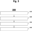
Fig. 3 shows a scheme of an embodiment of amethod 300 for testing at least one electronic assembly, comprising: providing at least one electronic assembly, wherein said electronic assembly comprises at least n magnetic storage cells, and wherein n is a natural number starting with 1, corresponding to positive integers, i.e. n = 1, 2, 3, ...; and at least one testing device with n read write electronics, wherein said read-write electronics are adapted to said at least one saidstorage cell 310; arranging said testing device above said electronic assembly so that each of said read-write electronics is located without contact on top of onerespective storage cell 320; writing at least one of saidstorage cells 520 by means of saidtesting device 330; and reading out at least saidstorage cell 320 by means of saidtesting device 340. -
Fig. 4 shows scheme of an embodiment of amethod 400, based onmethod 300 described above, wherein said electronic assembly further comprises at least m logic gates, wherein m is a natural number starting with 0, corresponding to non-negative integers, i.e. m = 0, 1, 2, 3, ...; and wherein at least one of said magnetic storage cells and one of said logic gates provides at least one electrically conductive connection. Furthermore,method 400 comprises further at least the following steps: writing all said magnetic storage cells by means of said testing device with a firsttest data set 430; triggering subsequently said electronic assembly to operate for at least one singlesystem clock pulse 435; and reading out all subsequently saidmagnetic storage cells 440. -
Fig. 5A shows a schematic top view of anembodiment 500A of devices according to the claimed invention in this present application. Theembodiment 500A of devices comprises at least anelectronic assembly 510 comprising at least onemagnetic storage cell 520 and at least one logic gate, wherein said magnetic storage cell and said logic gate are electrically conductive connected by means of at least one electricallyconductive connection 560. -
Fig. 5B shows a schematic cross-section of anembodiment 500B of devices according to the claimed invention in this present application. Theembodiment 500B of devices comprises at least anelectronic assembly 510 comprising at least onemagnetic storage cell 520 and at least one logic gate, wherein said magnetic storage cell and said logic gate are electrically conductive connected by means of at least one electricallyconductive connection 560. Furthermore,embodiment 500B comprises at least onetesting device 530 with at least one read write electronic 540. -
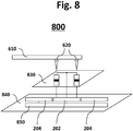
Fig. 6 shows a zoomed out schematic cross-section of an embodiment of a device to carry out the method according to one of the claims. In other words,Fig. 6 shows a zoom-out picture of the below describedFig. 8. Fig. 8 represents the diagram for a single flip-flop, whereasFig. 6 represents the full chip where several flip-flops are placed. Therefore, some of the terminologies which we have used forFig. 6 is also interchangeable with other figures.Fig. 6 describes the testing method according to the claimed invention in this present application at chip-level. As conventional testing method, it consists of amagnetic probes 610, several probingpins 620 and the design undertest 630. During the testing, probing knobs (e.g. pins) are adjusted on one of the MTJs of each flip-flops 640, which are analogous to 200A, 200B, and 200C, as described below inFig. 8 . Once these are adjusted, the value to be stored is activated through the probingpins 620 that are programed through the magnetic probe station. Thereafter, in the similar way, the opposite value has to be stored in the other MTJ cell of the each flip-flops 640. The rest of the sequence of the operation is as explained in the followingFig. 7 . -
Fig. 7 shows a schematic flowchart of anembodiment 700 of a method according to one of the claims. The method represented by theembodiment 700 is described as follows: - In
step 710 the magnetic probes are configured to perform subsequently a testing method according to one of the claims. Instep 720 values for respective MTJs of corresponding flip-flops are set or written. Instep 730 the clock is triggered to access CMOS logic. Instep 740 the respective value is propagated to next flip-flop. Instep 750 the respective values are read from MTJs using magnetic probe. Thesteps 710 to 750 may be repeated one or more times. Subsequently, i.e. instep 760, the respective value will be compared with the golden data, i.e. a default value or set of values or data. One of two results are feasible fromstep 760. In case of a mismatch between respective value and golden data the test is deemed to be failed - 760. In case of a match between respective value and golden data the test is deemed to be passed. -
Fig. 8 shows a schematic representation of anembodiment 800 of an exemplary device to carry out the method according to one of theclaims 1 to 3. A magnetic probe or magnetic probe system 810 with exemplary twoprobing pins 620, whereas such amagnetic probe 610 may provide one or moreprobing pins 620. The probing pins 620 are arranged over a correspondingmagnetic layer 830, whereas themagnetic layer 830, is the layer of the fabrication process in which MTJ cells are fabricated and comprises different processes and materials compared to common process layers, wherein all the MTJ cell are fabricated in the magnetic layer, is here formed exemplary by or comprises two exemplary MTJs. Themagnetic layer 830 is electrical conductive connected with at least two writecomponents 204, i.e. each with one of the respective MTJs of themagnetic layer 830, and with at least aread component 202. Further thewrite components 204 and theread component 202 are electrical conductive connected with at least one conventional flip-flop 850, respectively, whereas the flip-flop 850 is arranged on top of a so-calledCMOS layer 840. All the CMOS components are fabricated in thisCMOS layer 840. These have certain standard processes for the fabrications and in order to separate it from magnetic layers (in which MTJs are placed).Table of reference signs: 100A Basic test method 102 Test vector 104 Design under test 106 Analysis 108 Inputs 110 Outputs 112 Results 100B Flip-flop and scan-chain flip-flop structure 114 Data input 116 Clk (= Clock) 118 Arrow represents "replaced with" 120 Test input 122 Test enable 124 Mux 126 Flip-flop 128 Q or Test output 100C Embodiment of a conventional scan-chain method 130 Combinational logic 200A Non-volatile latch 202 Read component 204 Write component 206 Magnetic tunnel junction (MTJ) 208 Data 210 MTJ_read 200B Shadow flip-flop architecture acc. to [2] 212 Data 214 PD 216 Conventional CMOS flip-flop 218 Master latch 220 Slave latch 222 Non-volatile latch 200C Non-shadow flip-flop architecture acc. to [3] 300 Embodiment of a method according to claim 1 310 First method step according to claim 1 or 3 320 Second method step according to claim 1 or 3 330 Third method step according to claim 1 340 Fourth method step according to claim 1 400 Embodiment of a method according to claim 3 430 Third method step according to claim 3 435 Fourth method step according to claim 3 440 Fifth method step according to claim 3 500A Embodiment of an electronic assembly according to claims 2 or 3 500B Embodiment of an electronic assembly and a testing device according to claims 2 or 3 510 Electronic assembly 520 Magnetic storage cell 530 Testing device 540 Read write electronic 550 Logic gate 560 Electrically conductive connection 600 Schematic embodiment of a method acc. to one of the claims 1 to 3 610 Magnetic probes 620 Probing pin 630 Design under test (DUT), e.g. Chip 640 Flip-flops using MTJ cell 700 Flow-chart of an embodiment of a method according to one of the claims 1 to 3 710 Configuring magnetic probes 720 Setting values for MTJs of corresponding flip-flops using magnetic probes 730 Triggering clock to access CMOS logic 740 Propagating value to next flip-flop 750 Reading values from MTJs using magnetic probes 760 Comparing the value with golden data 765 Mismatch 770 Failing 775 Match 780 Pass 800 Schematic Embodiment to demonstrate accessing MTJ's using magnetic probes 830 Magnetic layer 840 CMOS layer 850 Conventional flip-flop
Claims (3)
- Method (300, 400) for testing at least one electronic assembly (510), comprising:a. Providing:i. at least one electronic assembly (510),1. wherein said electronic assembly comprises at least n magnetic storage cells (520),
and2. wherein n is a natural number starting with 1, corresponding to positive integers,and
i.e. n = 1, 2, 3, ...;ii. at least one testing device (530) with n read-write electronics (540),1. wherein said read-write electronics (540) are adapted to said at least one said storage cell (520) - (310);b. Arranging said testing device (330) above said electronic assembly (410) so that each of said read-write electronics (440) is located without contact on top of one respective storage cell (520) - (320);c. Writing at least one of said storage cells (520) by means of said testing device (530) - (330);
andd. Reading out at least said storage cell (320) by means of said testing device (530) - (340). - Method (100, 400) according to claim 1,a. wherein said electronic assembly (510) further comprises at least m logic gates (550),i. wherein m is a natural number starting with 0, corresponding to non-negative integers,and
i.e. m = 0, 1, 2, 3, ...;b. wherein at least one of said magnetic storage cells (520) and one of said logic gates (550) provides at least one electrically conductive connection (560). - Method (400) according to claim 2, further comprises:a. writing all said magnetic storage cells by means of said testing device with a first test data set - (430);b. triggering subsequently said electronic assembly to operate for at least one single system clock pulse - (435);
andc. reading out subsequently all said magnetic storage cells by means of said testing device - (440).
Priority Applications (1)
| Application Number | Priority Date | Filing Date | Title |
|---|---|---|---|
| EP17401042.1A EP3388849B1 (en) | 2017-04-11 | 2017-04-11 | Magnetic probe based test method for spintronic technologies |
Applications Claiming Priority (1)
| Application Number | Priority Date | Filing Date | Title |
|---|---|---|---|
| EP17401042.1A EP3388849B1 (en) | 2017-04-11 | 2017-04-11 | Magnetic probe based test method for spintronic technologies |
Publications (2)
| Publication Number | Publication Date |
|---|---|
| EP3388849A1 true EP3388849A1 (en) | 2018-10-17 |
| EP3388849B1 EP3388849B1 (en) | 2022-06-08 |
Family
ID=58671558
Family Applications (1)
| Application Number | Title | Priority Date | Filing Date |
|---|---|---|---|
| EP17401042.1A Active EP3388849B1 (en) | 2017-04-11 | 2017-04-11 | Magnetic probe based test method for spintronic technologies |
Country Status (1)
| Country | Link |
|---|---|
| EP (1) | EP3388849B1 (en) |
Citations (3)
| Publication number | Priority date | Publication date | Assignee | Title |
|---|---|---|---|---|
| US7165197B2 (en) * | 2003-11-24 | 2007-01-16 | Samsung Electronics Co., Ltd. | Apparatus and method of analyzing a magnetic random access memory |
| US20160104502A1 (en) * | 2013-12-17 | 2016-04-14 | U.S. Army Research Laboratory Attn: Rdrl-Loc-I | Read-write non-erasable memory with laser recording and method of recording |
| US20170059669A1 (en) * | 2015-08-26 | 2017-03-02 | Qualcomm Incorporated | Magnetic field enhancing backing plate for mram wafer testing |
-
2017
- 2017-04-11 EP EP17401042.1A patent/EP3388849B1/en active Active
Patent Citations (3)
| Publication number | Priority date | Publication date | Assignee | Title |
|---|---|---|---|---|
| US7165197B2 (en) * | 2003-11-24 | 2007-01-16 | Samsung Electronics Co., Ltd. | Apparatus and method of analyzing a magnetic random access memory |
| US20160104502A1 (en) * | 2013-12-17 | 2016-04-14 | U.S. Army Research Laboratory Attn: Rdrl-Loc-I | Read-write non-erasable memory with laser recording and method of recording |
| US20170059669A1 (en) * | 2015-08-26 | 2017-03-02 | Qualcomm Incorporated | Magnetic field enhancing backing plate for mram wafer testing |
Non-Patent Citations (4)
| Title |
|---|
| NEIL H.E. WESTE; DAVID HARRIS: "CMOS VLSI Design: A Circuit and System Perspective", 2004, ADDISON WESLEY, pages: 596 |
| R. BISHNOI; F. OBORIL; M.B. TAHOORI.: "Fault Tolerant Non-Volatile Spintronic Flip-Flop", DATE CONFERENCE, 2016, pages 261 - 264 |
| R. BISHNOI; F. OBORIL; M.B. TAHOORI.: "Non-Volatile Non-Shadow Flip-Flop using Spin Orbit Torque for Efficient Normally-off Computing", ASPDAC CONFERENCE, 2016, pages 769 - 774, XP032877679, DOI: doi:10.1109/ASPDAC.2016.7428104 |
| R. ROBERTAZZI; I. NOWAK; I. SUN: "Analytical MRAM test", ITC CONFERENCE, 2014, pages 1 - 10 |
Also Published As
| Publication number | Publication date |
|---|---|
| EP3388849B1 (en) | 2022-06-08 |
Similar Documents
| Publication | Publication Date | Title |
|---|---|---|
| US4051352A (en) | Level sensitive embedded array logic system | |
| Sakimura et al. | Nonvolatile magnetic flip-flop for standby-power-free SoCs | |
| US3783254A (en) | Level sensitive logic system | |
| US4608669A (en) | Self contained array timing | |
| US5870411A (en) | Method and system for testing self-timed circuitry | |
| JPH0465350B2 (en) | ||
| US4852061A (en) | High density, high performance register file having improved clocking means | |
| US9098486B1 (en) | Methods and apparatus for testing multiple clock domain memories | |
| US10110234B1 (en) | Efficient system debug infrastructure for tiled architecture | |
| US10229748B1 (en) | Memory interface latch with integrated write-through function | |
| US12243604B1 (en) | Scannable memory array and a method for scanning memory | |
| US10916323B2 (en) | Memory interface latch with integrated write-through and fence functions | |
| EP3388849B1 (en) | Magnetic probe based test method for spintronic technologies | |
| Gericota et al. | Active replication: Towards a truly SRAM-based FPGA on-line concurrent testing | |
| TWI877912B (en) | Semiconductor device and method for operating semiconductor device | |
| Kumari et al. | FPGA implementation of memory design and testing | |
| Zarrineh et al. | Self test architecture for testing complex memory structures | |
| Tran et al. | A new hybrid fault-tolerant architecture for digital cmos circuits and systems | |
| CN222927205U (en) | Input/output circuit and memory circuit | |
| Tan et al. | A Multi-mode Configuration Circuit Design for SoPC | |
| Jone et al. | An efficient BIST method for non-traditional faults of embedded memory arrays | |
| Nigh | Built-in current testing | |
| US12488176B1 (en) | Systems and methods for reducing test point power consumption in a circuit design | |
| EP0288774B1 (en) | High density, high performance register file circuit | |
| Gericota et al. | On-line Testing of FPGA Logic Blocks Using Active Replication |
Legal Events
| Date | Code | Title | Description |
|---|---|---|---|
| PUAI | Public reference made under article 153(3) epc to a published international application that has entered the european phase |
Free format text: ORIGINAL CODE: 0009012 |
|
| STAA | Information on the status of an ep patent application or granted ep patent |
Free format text: STATUS: THE APPLICATION HAS BEEN PUBLISHED |
|
| AK | Designated contracting states |
Kind code of ref document: A1 Designated state(s): AL AT BE BG CH CY CZ DE DK EE ES FI FR GB GR HR HU IE IS IT LI LT LU LV MC MK MT NL NO PL PT RO RS SE SI SK SM TR |
|
| AX | Request for extension of the european patent |
Extension state: BA ME |
|
| STAA | Information on the status of an ep patent application or granted ep patent |
Free format text: STATUS: REQUEST FOR EXAMINATION WAS MADE |
|
| 17P | Request for examination filed |
Effective date: 20190417 |
|
| RBV | Designated contracting states (corrected) |
Designated state(s): AL AT BE BG CH CY CZ DE DK EE ES FI FR GB GR HR HU IE IS IT LI LT LU LV MC MK MT NL NO PL PT RO RS SE SI SK SM TR |
|
| GRAP | Despatch of communication of intention to grant a patent |
Free format text: ORIGINAL CODE: EPIDOSNIGR1 |
|
| STAA | Information on the status of an ep patent application or granted ep patent |
Free format text: STATUS: GRANT OF PATENT IS INTENDED |
|
| RIC1 | Information provided on ipc code assigned before grant |
Ipc: G11C 29/56 20060101ALI20220208BHEP Ipc: G11C 29/32 20060101ALI20220208BHEP Ipc: G01R 1/07 20060101ALI20220208BHEP Ipc: G11C 29/00 20060101ALI20220208BHEP Ipc: G01R 31/303 20060101AFI20220208BHEP |
|
| INTG | Intention to grant announced |
Effective date: 20220224 |
|
| GRAS | Grant fee paid |
Free format text: ORIGINAL CODE: EPIDOSNIGR3 |
|
| GRAA | (expected) grant |
Free format text: ORIGINAL CODE: 0009210 |
|
| STAA | Information on the status of an ep patent application or granted ep patent |
Free format text: STATUS: THE PATENT HAS BEEN GRANTED |
|
| AK | Designated contracting states |
Kind code of ref document: B1 Designated state(s): AL AT BE BG CH CY CZ DE DK EE ES FI FR GB GR HR HU IE IS IT LI LT LU LV MC MK MT NL NO PL PT RO RS SE SI SK SM TR |
|
| REG | Reference to a national code |
Ref country code: AT Ref legal event code: REF Ref document number: 1497285 Country of ref document: AT Kind code of ref document: T Effective date: 20220615 Ref country code: CH Ref legal event code: EP |
|
| REG | Reference to a national code |
Ref country code: DE Ref legal event code: R096 Ref document number: 602017058252 Country of ref document: DE |
|
| REG | Reference to a national code |
Ref country code: IE Ref legal event code: FG4D |
|
| REG | Reference to a national code |
Ref country code: LT Ref legal event code: MG9D |
|
| REG | Reference to a national code |
Ref country code: NL Ref legal event code: MP Effective date: 20220608 |
|
| PG25 | Lapsed in a contracting state [announced via postgrant information from national office to epo] |
Ref country code: SE Free format text: LAPSE BECAUSE OF FAILURE TO SUBMIT A TRANSLATION OF THE DESCRIPTION OR TO PAY THE FEE WITHIN THE PRESCRIBED TIME-LIMIT Effective date: 20220608 Ref country code: NO Free format text: LAPSE BECAUSE OF FAILURE TO SUBMIT A TRANSLATION OF THE DESCRIPTION OR TO PAY THE FEE WITHIN THE PRESCRIBED TIME-LIMIT Effective date: 20220908 Ref country code: LT Free format text: LAPSE BECAUSE OF FAILURE TO SUBMIT A TRANSLATION OF THE DESCRIPTION OR TO PAY THE FEE WITHIN THE PRESCRIBED TIME-LIMIT Effective date: 20220608 Ref country code: HR Free format text: LAPSE BECAUSE OF FAILURE TO SUBMIT A TRANSLATION OF THE DESCRIPTION OR TO PAY THE FEE WITHIN THE PRESCRIBED TIME-LIMIT Effective date: 20220608 Ref country code: GR Free format text: LAPSE BECAUSE OF FAILURE TO SUBMIT A TRANSLATION OF THE DESCRIPTION OR TO PAY THE FEE WITHIN THE PRESCRIBED TIME-LIMIT Effective date: 20220909 Ref country code: FI Free format text: LAPSE BECAUSE OF FAILURE TO SUBMIT A TRANSLATION OF THE DESCRIPTION OR TO PAY THE FEE WITHIN THE PRESCRIBED TIME-LIMIT Effective date: 20220608 Ref country code: ES Free format text: LAPSE BECAUSE OF FAILURE TO SUBMIT A TRANSLATION OF THE DESCRIPTION OR TO PAY THE FEE WITHIN THE PRESCRIBED TIME-LIMIT Effective date: 20220608 Ref country code: BG Free format text: LAPSE BECAUSE OF FAILURE TO SUBMIT A TRANSLATION OF THE DESCRIPTION OR TO PAY THE FEE WITHIN THE PRESCRIBED TIME-LIMIT Effective date: 20220908 |
|
| REG | Reference to a national code |
Ref country code: AT Ref legal event code: MK05 Ref document number: 1497285 Country of ref document: AT Kind code of ref document: T Effective date: 20220608 |
|
| PG25 | Lapsed in a contracting state [announced via postgrant information from national office to epo] |
Ref country code: RS Free format text: LAPSE BECAUSE OF FAILURE TO SUBMIT A TRANSLATION OF THE DESCRIPTION OR TO PAY THE FEE WITHIN THE PRESCRIBED TIME-LIMIT Effective date: 20220608 Ref country code: LV Free format text: LAPSE BECAUSE OF FAILURE TO SUBMIT A TRANSLATION OF THE DESCRIPTION OR TO PAY THE FEE WITHIN THE PRESCRIBED TIME-LIMIT Effective date: 20220608 |
|
| PG25 | Lapsed in a contracting state [announced via postgrant information from national office to epo] |
Ref country code: NL Free format text: LAPSE BECAUSE OF FAILURE TO SUBMIT A TRANSLATION OF THE DESCRIPTION OR TO PAY THE FEE WITHIN THE PRESCRIBED TIME-LIMIT Effective date: 20220608 |
|
| PG25 | Lapsed in a contracting state [announced via postgrant information from national office to epo] |
Ref country code: SM Free format text: LAPSE BECAUSE OF FAILURE TO SUBMIT A TRANSLATION OF THE DESCRIPTION OR TO PAY THE FEE WITHIN THE PRESCRIBED TIME-LIMIT Effective date: 20220608 Ref country code: SK Free format text: LAPSE BECAUSE OF FAILURE TO SUBMIT A TRANSLATION OF THE DESCRIPTION OR TO PAY THE FEE WITHIN THE PRESCRIBED TIME-LIMIT Effective date: 20220608 Ref country code: RO Free format text: LAPSE BECAUSE OF FAILURE TO SUBMIT A TRANSLATION OF THE DESCRIPTION OR TO PAY THE FEE WITHIN THE PRESCRIBED TIME-LIMIT Effective date: 20220608 Ref country code: PT Free format text: LAPSE BECAUSE OF FAILURE TO SUBMIT A TRANSLATION OF THE DESCRIPTION OR TO PAY THE FEE WITHIN THE PRESCRIBED TIME-LIMIT Effective date: 20221010 Ref country code: EE Free format text: LAPSE BECAUSE OF FAILURE TO SUBMIT A TRANSLATION OF THE DESCRIPTION OR TO PAY THE FEE WITHIN THE PRESCRIBED TIME-LIMIT Effective date: 20220608 Ref country code: CZ Free format text: LAPSE BECAUSE OF FAILURE TO SUBMIT A TRANSLATION OF THE DESCRIPTION OR TO PAY THE FEE WITHIN THE PRESCRIBED TIME-LIMIT Effective date: 20220608 Ref country code: AT Free format text: LAPSE BECAUSE OF FAILURE TO SUBMIT A TRANSLATION OF THE DESCRIPTION OR TO PAY THE FEE WITHIN THE PRESCRIBED TIME-LIMIT Effective date: 20220608 |
|
| PG25 | Lapsed in a contracting state [announced via postgrant information from national office to epo] |
Ref country code: PL Free format text: LAPSE BECAUSE OF FAILURE TO SUBMIT A TRANSLATION OF THE DESCRIPTION OR TO PAY THE FEE WITHIN THE PRESCRIBED TIME-LIMIT Effective date: 20220608 Ref country code: IS Free format text: LAPSE BECAUSE OF FAILURE TO SUBMIT A TRANSLATION OF THE DESCRIPTION OR TO PAY THE FEE WITHIN THE PRESCRIBED TIME-LIMIT Effective date: 20221008 |
|
| REG | Reference to a national code |
Ref country code: DE Ref legal event code: R097 Ref document number: 602017058252 Country of ref document: DE |
|
| PG25 | Lapsed in a contracting state [announced via postgrant information from national office to epo] |
Ref country code: AL Free format text: LAPSE BECAUSE OF FAILURE TO SUBMIT A TRANSLATION OF THE DESCRIPTION OR TO PAY THE FEE WITHIN THE PRESCRIBED TIME-LIMIT Effective date: 20220608 |
|
| PLBE | No opposition filed within time limit |
Free format text: ORIGINAL CODE: 0009261 |
|
| STAA | Information on the status of an ep patent application or granted ep patent |
Free format text: STATUS: NO OPPOSITION FILED WITHIN TIME LIMIT |
|
| PG25 | Lapsed in a contracting state [announced via postgrant information from national office to epo] |
Ref country code: DK Free format text: LAPSE BECAUSE OF FAILURE TO SUBMIT A TRANSLATION OF THE DESCRIPTION OR TO PAY THE FEE WITHIN THE PRESCRIBED TIME-LIMIT Effective date: 20220608 |
|
| 26N | No opposition filed |
Effective date: 20230310 |
|
| PG25 | Lapsed in a contracting state [announced via postgrant information from national office to epo] |
Ref country code: SI Free format text: LAPSE BECAUSE OF FAILURE TO SUBMIT A TRANSLATION OF THE DESCRIPTION OR TO PAY THE FEE WITHIN THE PRESCRIBED TIME-LIMIT Effective date: 20220608 |
|
| REG | Reference to a national code |
Ref country code: CH Ref legal event code: PL |
|
| PG25 | Lapsed in a contracting state [announced via postgrant information from national office to epo] |
Ref country code: LU Free format text: LAPSE BECAUSE OF NON-PAYMENT OF DUE FEES Effective date: 20230411 |
|
| PG25 | Lapsed in a contracting state [announced via postgrant information from national office to epo] |
Ref country code: MC Free format text: LAPSE BECAUSE OF FAILURE TO SUBMIT A TRANSLATION OF THE DESCRIPTION OR TO PAY THE FEE WITHIN THE PRESCRIBED TIME-LIMIT Effective date: 20220608 |
|
| PG25 | Lapsed in a contracting state [announced via postgrant information from national office to epo] |
Ref country code: MC Free format text: LAPSE BECAUSE OF FAILURE TO SUBMIT A TRANSLATION OF THE DESCRIPTION OR TO PAY THE FEE WITHIN THE PRESCRIBED TIME-LIMIT Effective date: 20220608 Ref country code: LI Free format text: LAPSE BECAUSE OF NON-PAYMENT OF DUE FEES Effective date: 20230430 Ref country code: IT Free format text: LAPSE BECAUSE OF FAILURE TO SUBMIT A TRANSLATION OF THE DESCRIPTION OR TO PAY THE FEE WITHIN THE PRESCRIBED TIME-LIMIT Effective date: 20220608 Ref country code: CH Free format text: LAPSE BECAUSE OF NON-PAYMENT OF DUE FEES Effective date: 20230430 |
|
| REG | Reference to a national code |
Ref country code: IE Ref legal event code: MM4A |
|
| PG25 | Lapsed in a contracting state [announced via postgrant information from national office to epo] |
Ref country code: IE Free format text: LAPSE BECAUSE OF NON-PAYMENT OF DUE FEES Effective date: 20230411 |
|
| PG25 | Lapsed in a contracting state [announced via postgrant information from national office to epo] |
Ref country code: IE Free format text: LAPSE BECAUSE OF NON-PAYMENT OF DUE FEES Effective date: 20230411 |
|
| PG25 | Lapsed in a contracting state [announced via postgrant information from national office to epo] |
Ref country code: BG Free format text: LAPSE BECAUSE OF FAILURE TO SUBMIT A TRANSLATION OF THE DESCRIPTION OR TO PAY THE FEE WITHIN THE PRESCRIBED TIME-LIMIT Effective date: 20220608 |
|
| PG25 | Lapsed in a contracting state [announced via postgrant information from national office to epo] |
Ref country code: BG Free format text: LAPSE BECAUSE OF FAILURE TO SUBMIT A TRANSLATION OF THE DESCRIPTION OR TO PAY THE FEE WITHIN THE PRESCRIBED TIME-LIMIT Effective date: 20220608 |
|
| PGFP | Annual fee paid to national office [announced via postgrant information from national office to epo] |
Ref country code: DE Payment date: 20250417 Year of fee payment: 9 |
|
| PGFP | Annual fee paid to national office [announced via postgrant information from national office to epo] |
Ref country code: BE Payment date: 20250422 Year of fee payment: 9 |
|
| PGFP | Annual fee paid to national office [announced via postgrant information from national office to epo] |
Ref country code: FR Payment date: 20250422 Year of fee payment: 9 |
|
| PG25 | Lapsed in a contracting state [announced via postgrant information from national office to epo] |
Ref country code: CY Free format text: LAPSE BECAUSE OF FAILURE TO SUBMIT A TRANSLATION OF THE DESCRIPTION OR TO PAY THE FEE WITHIN THE PRESCRIBED TIME-LIMIT; INVALID AB INITIO Effective date: 20170411 |
|
| PG25 | Lapsed in a contracting state [announced via postgrant information from national office to epo] |
Ref country code: HU Free format text: LAPSE BECAUSE OF FAILURE TO SUBMIT A TRANSLATION OF THE DESCRIPTION OR TO PAY THE FEE WITHIN THE PRESCRIBED TIME-LIMIT; INVALID AB INITIO Effective date: 20170411 |
|
| PG25 | Lapsed in a contracting state [announced via postgrant information from national office to epo] |
Ref country code: TR Free format text: LAPSE BECAUSE OF FAILURE TO SUBMIT A TRANSLATION OF THE DESCRIPTION OR TO PAY THE FEE WITHIN THE PRESCRIBED TIME-LIMIT Effective date: 20220608 |
|
| PGFP | Annual fee paid to national office [announced via postgrant information from national office to epo] |
Ref country code: GB Payment date: 20260324 Year of fee payment: 10 |