EP3382889A1 - Control device for electric machine, and electric vehicle using same - Google Patents
Control device for electric machine, and electric vehicle using same Download PDFInfo
- Publication number
- EP3382889A1 EP3382889A1 EP16868299.5A EP16868299A EP3382889A1 EP 3382889 A1 EP3382889 A1 EP 3382889A1 EP 16868299 A EP16868299 A EP 16868299A EP 3382889 A1 EP3382889 A1 EP 3382889A1
- Authority
- EP
- European Patent Office
- Prior art keywords
- phase
- zero
- current
- period
- motor
- Prior art date
- Legal status (The legal status is an assumption and is not a legal conclusion. Google has not performed a legal analysis and makes no representation as to the accuracy of the status listed.)
- Granted
Links
Images


Classifications
-
- B—PERFORMING OPERATIONS; TRANSPORTING
- B60—VEHICLES IN GENERAL
- B60L—PROPULSION OF ELECTRICALLY-PROPELLED VEHICLES; SUPPLYING ELECTRIC POWER FOR AUXILIARY EQUIPMENT OF ELECTRICALLY-PROPELLED VEHICLES; ELECTRODYNAMIC BRAKE SYSTEMS FOR VEHICLES IN GENERAL; MAGNETIC SUSPENSION OR LEVITATION FOR VEHICLES; MONITORING OPERATING VARIABLES OF ELECTRICALLY-PROPELLED VEHICLES; ELECTRIC SAFETY DEVICES FOR ELECTRICALLY-PROPELLED VEHICLES
- B60L3/00—Electric devices on electrically-propelled vehicles for safety purposes; Monitoring operating variables, e.g. speed, deceleration or energy consumption
- B60L3/0023—Detecting, eliminating, remedying or compensating for drive train abnormalities, e.g. failures within the drive train
- B60L3/0038—Detecting, eliminating, remedying or compensating for drive train abnormalities, e.g. failures within the drive train relating to sensors
-
- H—ELECTRICITY
- H02—GENERATION; CONVERSION OR DISTRIBUTION OF ELECTRIC POWER
- H02P—CONTROL OR REGULATION OF ELECTRIC MOTORS, ELECTRIC GENERATORS OR DYNAMO-ELECTRIC CONVERTERS; CONTROLLING TRANSFORMERS, REACTORS OR CHOKE COILS
- H02P21/00—Arrangements or methods for the control of electric machines by vector control, e.g. by control of field orientation
- H02P21/22—Current control, e.g. using a current control loop
-
- B—PERFORMING OPERATIONS; TRANSPORTING
- B60—VEHICLES IN GENERAL
- B60L—PROPULSION OF ELECTRICALLY-PROPELLED VEHICLES; SUPPLYING ELECTRIC POWER FOR AUXILIARY EQUIPMENT OF ELECTRICALLY-PROPELLED VEHICLES; ELECTRODYNAMIC BRAKE SYSTEMS FOR VEHICLES IN GENERAL; MAGNETIC SUSPENSION OR LEVITATION FOR VEHICLES; MONITORING OPERATING VARIABLES OF ELECTRICALLY-PROPELLED VEHICLES; ELECTRIC SAFETY DEVICES FOR ELECTRICALLY-PROPELLED VEHICLES
- B60L3/00—Electric devices on electrically-propelled vehicles for safety purposes; Monitoring operating variables, e.g. speed, deceleration or energy consumption
- B60L3/0023—Detecting, eliminating, remedying or compensating for drive train abnormalities, e.g. failures within the drive train
- B60L3/0061—Detecting, eliminating, remedying or compensating for drive train abnormalities, e.g. failures within the drive train relating to electrical machines
-
- B—PERFORMING OPERATIONS; TRANSPORTING
- B60—VEHICLES IN GENERAL
- B60L—PROPULSION OF ELECTRICALLY-PROPELLED VEHICLES; SUPPLYING ELECTRIC POWER FOR AUXILIARY EQUIPMENT OF ELECTRICALLY-PROPELLED VEHICLES; ELECTRODYNAMIC BRAKE SYSTEMS FOR VEHICLES IN GENERAL; MAGNETIC SUSPENSION OR LEVITATION FOR VEHICLES; MONITORING OPERATING VARIABLES OF ELECTRICALLY-PROPELLED VEHICLES; ELECTRIC SAFETY DEVICES FOR ELECTRICALLY-PROPELLED VEHICLES
- B60L3/00—Electric devices on electrically-propelled vehicles for safety purposes; Monitoring operating variables, e.g. speed, deceleration or energy consumption
- B60L3/12—Recording operating variables ; Monitoring of operating variables
-
- B—PERFORMING OPERATIONS; TRANSPORTING
- B60—VEHICLES IN GENERAL
- B60L—PROPULSION OF ELECTRICALLY-PROPELLED VEHICLES; SUPPLYING ELECTRIC POWER FOR AUXILIARY EQUIPMENT OF ELECTRICALLY-PROPELLED VEHICLES; ELECTRODYNAMIC BRAKE SYSTEMS FOR VEHICLES IN GENERAL; MAGNETIC SUSPENSION OR LEVITATION FOR VEHICLES; MONITORING OPERATING VARIABLES OF ELECTRICALLY-PROPELLED VEHICLES; ELECTRIC SAFETY DEVICES FOR ELECTRICALLY-PROPELLED VEHICLES
- B60L50/00—Electric propulsion with power supplied within the vehicle
- B60L50/50—Electric propulsion with power supplied within the vehicle using propulsion power supplied by batteries or fuel cells
- B60L50/60—Electric propulsion with power supplied within the vehicle using propulsion power supplied by batteries or fuel cells using power supplied by batteries
-
- H—ELECTRICITY
- H02—GENERATION; CONVERSION OR DISTRIBUTION OF ELECTRIC POWER
- H02P—CONTROL OR REGULATION OF ELECTRIC MOTORS, ELECTRIC GENERATORS OR DYNAMO-ELECTRIC CONVERTERS; CONTROLLING TRANSFORMERS, REACTORS OR CHOKE COILS
- H02P27/00—Arrangements or methods for the control of AC motors characterised by the kind of supply voltage
- H02P27/04—Arrangements or methods for the control of AC motors characterised by the kind of supply voltage using variable-frequency supply voltage, e.g. inverter or converter supply voltage
- H02P27/06—Arrangements or methods for the control of AC motors characterised by the kind of supply voltage using variable-frequency supply voltage, e.g. inverter or converter supply voltage using DC to AC converters or inverters
- H02P27/08—Arrangements or methods for the control of AC motors characterised by the kind of supply voltage using variable-frequency supply voltage, e.g. inverter or converter supply voltage using DC to AC converters or inverters with pulse width modulation
- H02P27/12—Arrangements or methods for the control of AC motors characterised by the kind of supply voltage using variable-frequency supply voltage, e.g. inverter or converter supply voltage using DC to AC converters or inverters with pulse width modulation pulsing by guiding the flux vector, current vector or voltage vector on a circle or a closed curve, e.g. for direct torque control
-
- H—ELECTRICITY
- H02—GENERATION; CONVERSION OR DISTRIBUTION OF ELECTRIC POWER
- H02P—CONTROL OR REGULATION OF ELECTRIC MOTORS, ELECTRIC GENERATORS OR DYNAMO-ELECTRIC CONVERTERS; CONTROLLING TRANSFORMERS, REACTORS OR CHOKE COILS
- H02P2209/00—Indexing scheme relating to controlling arrangements characterised by the waveform of the supplied voltage or current
- H02P2209/03—Motors with neutral point disassociated, i.e. the windings ends are not connected directly to a common point
-
- Y—GENERAL TAGGING OF NEW TECHNOLOGICAL DEVELOPMENTS; GENERAL TAGGING OF CROSS-SECTIONAL TECHNOLOGIES SPANNING OVER SEVERAL SECTIONS OF THE IPC; TECHNICAL SUBJECTS COVERED BY FORMER USPC CROSS-REFERENCE ART COLLECTIONS [XRACs] AND DIGESTS
- Y02—TECHNOLOGIES OR APPLICATIONS FOR MITIGATION OR ADAPTATION AGAINST CLIMATE CHANGE
- Y02T—CLIMATE CHANGE MITIGATION TECHNOLOGIES RELATED TO TRANSPORTATION
- Y02T10/00—Road transport of goods or passengers
- Y02T10/60—Other road transportation technologies with climate change mitigation effect
- Y02T10/70—Energy storage systems for electromobility, e.g. batteries
Definitions
- the present invention relates to a control device of a motor and an electric vehicle using the same.
- Hybrid vehicles and electric vehicles are desired to improve the output torque per unit volume of the vehicle from the viewpoint of improving the reliability from the viewpoint of preventing occurrence of failures while the vehicle is traveling and from the viewpoint of weight reduction of the vehicle.
- Three-phase 6-wire type driving devices are considered to respond to these demands, but since a motor not connected with a neutral point is used, 3n-th harmonic current is superimposed on the driving current for driving the motor, and there is a problem in that loss such as copper loss increases .
- PTL 1 JP 2004-80975 A
- 3n-th harmonic current (3 is the number of phases, n is an integer) included in the driving current for driving the motor is detected and the 3n-th harmonic voltage command value for canceling is calculated to correct the three-phase voltage command value. Accordingly, PTL 1 aims to correct the target voltage so as to cancel the 3n-th harmonic current, so that the harmonic current in the driving current can be removed and the loss due to the harmonic current can be reduced.
- a control device of a motor is a control device in which a winding is independently connected for each phase, the control device including: a control unit controlling a voltage applied to the motor on the basis of a torque command value, wherein the control unit provides a first period in which a zero-phase voltage pulse for outputting a zero-phase voltage for reducing a zero-phase current which is determined based on an alternating current of each phase is output, and a second period in which a current of each phase flowing in the motor is detected, and the first period and the second period are not overlapped.
- detection error of the zero-phase current can be reduced.
- FIG. 1 is a diagram showing a configuration of a motor drive system according to an embodiment of the present invention.
- the motor drive system includes a motor 200, a position sensor 210, a current sensor 220, an inverter 100, and a motor control device 1.
- the motor 200 is composed of an embedded magnet synchronous motor or the like to which a neutral point is not connected.
- the U-phase winding 201 wound around the stator of the motor 200 is connected to an output terminal of the U-phase full bridge inverter 110.
- the V-phase winding 202 wound around the stator of the motor 200 is connected to an output terminal of the V-phase full bridge inverter 111.
- the W-phase winding 203 wound around the stator of the motor 200 is connected to an output terminal of the W-phase full bridge inverter 112. Since the neutral point is not connected to the motor 200, it is possible to independently control the currents flowing through the U-phase winding 201, the V-phase winding 202, and the W-phase winding 203.. However, since the neutral point of the motor 200 is not connected, as described in PTL 1, the drive currents flowing through the U-phase winding 201, the V-phase winding 202, and the W-phase winding 203 include 3n-th harmonic current.
- the position sensor 210 detects the position of a rotor of the motor 200 and outputs the detected rotor position ⁇ .
- the current sensor 220 detects the currents flowing through the U-phase winding 201, the V-phase winding 202 and the W-phase winding 203 wound around the stator of the motor 200, and outputs the detected three-phase currents i u , i v , i w .
- the inverter 100 includes a U-phase full bridge inverter 110, a V-phase full bridge inverter 111, and a W-phase full bridge inverter 112.
- the U-phase full bridge inverter 110, the V-phase full bridge inverter 111, and the W-phase full bridge inverter 112 are connected in parallel to a direct current power supply (not shown).
- the U-phase full bridge inverter 110 is composed of switching elements 110a to 110d.
- the switching element 110a is arranged on a U-phase left leg upper arm.
- the switching element 110b is arranged on a U-phase left leg lower arm.
- the switching element 110c is arranged on a U-phase right leg upper arm.
- the switching element 110d is arranged on a U-phase right leg lower arm.
- the V-phase full bridge inverter 111 is composed of switching elements 111a to 111d.
- the switching element 111a is arranged on a V-phase left leg upper arm.
- the switching element 111b is arranged on a V-phase left leg lower arm.
- the switching element 111c is arranged on a V-phase right leg upper arm.
- the switching element 111d is arranged on a V-phase right leg lower arm.
- the W-phase full bridge inverter 112 is configured by switching elements 112a to 112d.
- the switching element 112a is arranged on a W-phase left leg upper arm.
- the switching element 112b is arranged on a W-phase left leg lower arm.
- the switching element 112c is arranged on a W-phase right leg upper arm.
- the switching element 112d is arranged on a W-phase right leg lower arm.
- the inverter 100 converts a direct current voltage applied from a direct current power supply (not shown) to an alternating current voltage.
- the converted alternating current voltage is applied to the three-phase windings 201 to 203 wound around the stator of the motor 200 to generate three-phase alternating current.
- This three-phase alternating current generates a rotating magnetic field in the motor 200, and the rotor rotates.
- the switching elements 110a to 110d, the switching elements 111a to 111d, and the switching elements 112a to 112d are formed by combining a metal oxide film type field effect transistor (MOSFET), an insulated gate bipolar transistor (IGBT) and the like, and diodes.
- MOSFET metal oxide film type field effect transistor
- IGBT insulated gate bipolar transistor
- the motor control device 1 PWM-controls the inverter 100 based on an external torque command T*, three-phase currents i u , i v , i w detected by the current sensor 220, and a rotor position ⁇ detected by the position sensor 210.
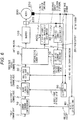
- FIG. 2 is a control block diagram explaining the first embodiment of the present invention.
- the current command computation unit 10 calculates the dq axis current command values i d *, i q * based on the input torque command value T* and the angular velocity ⁇ . Examples of the calculation method for calculating the dq axis current command values i d *, i q * include maximum torque current control, weak field control, and the like, but explanation thereabout is omitted since they are well known.
- a previously configured table may be used for calculation of the dq axis current command values i d *, i q *.
- the dq axis current control unit 20 receives the dq axis current command values i d *, i q * and the dq axis current detection values i d , i q , and outputs the dq axis voltage command value v d *, v q * using proportional control, integral control, and the like.
- the three-phase conversion unit 30 receives the dq axis voltage command values v d *, v q * and the rotor position ⁇ , and outputs the three-phase voltage command values v u *, v v *, v w *.
- the switching signal generation unit 40 receives the three-phase voltage command value v u *, v v *, v w *, the zero-phase voltage command value v 0 *, and the current detection timing signals t1, t2, and generates switching signals for turning on or off the switching elements 110a to 110d, the switching elements 111a to 111d, and the switching elements 112a to 112d.
- a switching signal is input to the inverter 100, and the motor is operated by the operation.
- the dq conversion unit 50 receives the three-phase current i u , i v , i w detected by the current sensor 220 and the rotor position ⁇ detected by the position sensor 210, and outputs the dq axis current detection values i d , i q .
- the zero-phase current calculation unit 60 receives the three-phase current i u , i v , i w detected by the current sensor 220 and the rotor position ⁇ detected by the position sensor 210, and outputs the zero-phase current i 0 .
- the zero-phase current i 0 may be calculated in consideration of the zero-phase current value estimated from the angular velocity ⁇ of the motor 200.
- the zero-phase current control unit 70 acquires the zero-phase current i 0 and outputs the zero-phase voltage command value v 0 by using proportional control, integral control, and the like.
- the velocity conversion unit 80 obtains the rotor position ⁇ detected by the position sensor 210 and outputs angular velocity ⁇ .
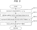
- FIG. 3 is a flowchart of the switching signal generation unit 40.
- the switching signal generation unit 40 calculates the U-phase voltage pulse width T U , the V-phase voltage pulse width T V , and the W-phase voltage pulse width T W on the basis of the three-phase voltage command value v u *, v v *, v w * output from the three-phase conversion unit 30, the zero-phase voltage command value v 0 * output from the zero-phase voltage control unit 70, the direct current power supply voltage V DC , the carrier frequency f carrier .
- pulses for outputting zero-phase voltage but in the following description, it is assumed that one pulse is output in each phase in one carrier cycle.
- step 2 the switching signal generation unit 40 obtains a current detection start timing t3 and a current detection end timing t4.
- step 3 the switching signal generation unit 40 calculates the zero-phase voltage output start timing t1 and the zero-phase voltage output end timing t2.
- the zero-phase voltage output start timing t1 and the zero-phase voltage output end timing t2 are configured to satisfy the relationship of the expression (5) or the expression (6).
- step 4 the switching signal generation unit 40 calculates timing for outputting the pulse of each phase on the basis of the U-phase voltage pulse width T U , the V-phase voltage pulse width T V , the W-phase voltage pulse width T W calculated in step 1, and the zero-phase voltage output start timing t1 and the zero-phase voltage output end timing t2 calculated in step 3.
- FIG. 4 is a diagram showing a waveform example of zero-phase voltage output timing when the present embodiment is applied.
- V 0 indicates a zero-phase voltage pulse.
- the U-phase pulse with the longest pulse width is output first. Therefore, the output timing of the U-phase pulse coincides with the zero-phase voltage output start timing t1. Next, at the zero-phase voltage output end timing, the V-phase pulse which is one phase of the remaining two phases is output. Finally, after the output of the V-phase pulse is completed, the pulse of the W-phase which is the remaining one phase is output. In the figure, the V-phase pulse is output first, but it is also possible to output the W-phase pulse first.
- t1 to t2 (e.g., the first period) during which the zero-phase voltage pulse V 0 is generated are set so as to avoid the current detection period from t3 to t4 (for example, the second period). Therefore, the pulse of each phase that does not generate a zero-phase voltage during the current detection period is output.
- the second period which is the current detection period may be set to avoid the first period in which the zero-phase voltage pulse V 0 is generated.
- FIG. 5 is a block diagram showing a second embodiment of the present invention.
- the block diagram shown in FIG. 5 is a configuration obtained by adding current detection timing computation 300 to the block diagram shown in FIG. 2 .
- the switching signal generation unit 40 not only generate the switching signal for turning on or off the switching elements 110a to 110d, the switching elements 111a to 111d, and the switching elements 112a to 112d as shown in FIG. 1 on the basis of the input three-phase voltage command values v u *, v v *, v w *, the zero-phase voltage command value v 0 *, and the current detection timing signal t3, t4, but also outputs the zero-phase voltage output timing t1, t2.
- the current detection timing computation 300 outputs the current detection start timing t3 and the current detection end timing t4 on the basis of the zero-phase voltage output start timing t1 and the zero-phase voltage output end timing t2, which have been input, so that the period in which the zero-phase voltage is output and the period in which the current is detected are not overlapped.
- FIG. 6 is a block diagram showing a third embodiment of the present invention.
- the block diagram shown in FIG. 6 is a configuration obtained by adding the zero-phase current calculation possibility determination 400 to the block diagram shown in FIG. 2 .
- the switching signal generation unit 40 not only generates switching signals for turning on or off the switching elements 110a to 110d, the switching element 111a to 111d, and the switching elements 112a to 112d shown in FIG. 1 on the basis of the input three-phase voltage command values v u *, v v *, v w * and the zero-phase voltage command value v 0 *, but also outputs the zero-phase voltage output timing signals t1, t2.
- the zero-phase current calculation possibility determination 400 determines whether the zero-phase voltage is output in the current detection period on the basis of the zero-phase voltage output start timing t1, the zero-phase voltage output end timing t2, the current detection start timing t3, and the current detection end timing t4, which are input. For example, the determination method is whether or not the t3 to t4, which are the current detection period, can be reserved in the 1 carrier cycle or not, and the like.
- a zero-phase current calculation end signal is output, and the calculation of zero-phase current at zero-phase current calculation unit 60 is ended in the corresponding carrier cycle.
- the effect that the detection error of the zero-phase current is reduced can be obtained by generating a period in which the zero-phase voltage is not output, and detecting the current in that period.
Landscapes
- Engineering & Computer Science (AREA)
- Power Engineering (AREA)
- Life Sciences & Earth Sciences (AREA)
- Sustainable Development (AREA)
- Sustainable Energy (AREA)
- Transportation (AREA)
- Mechanical Engineering (AREA)
- Control Of Ac Motors In General (AREA)
Abstract
Description
- The present invention relates to a control device of a motor and an electric vehicle using the same.
- Hybrid vehicles and electric vehicles are desired to improve the output torque per unit volume of the vehicle from the viewpoint of improving the reliability from the viewpoint of preventing occurrence of failures while the vehicle is traveling and from the viewpoint of weight reduction of the vehicle. Three-phase 6-wire type driving devices are considered to respond to these demands, but since a motor not connected with a neutral point is used, 3n-th harmonic current is superimposed on the driving current for driving the motor, and there is a problem in that loss such as copper loss increases .
- As background technology in this technical field, there is
JP 2004-80975 A PTL 1, "3n-th harmonic current (3 is the number of phases, n is an integer) included in the driving current for driving the motor is detected and the 3n-th harmonic voltage command value for canceling is calculated to correct the three-phase voltage command value". Accordingly,PTL 1 aims to correct the target voltage so as to cancel the 3n-th harmonic current, so that the harmonic current in the driving current can be removed and the loss due to the harmonic current can be reduced. - PTL 1:
JP 2004-80975 A - If a zero-phase voltage is output during the current detection period, an error may occur in the detected value of the zero-phase current, and the zero-phase current cannot be removed.
- It is an object of the present invention to reduce detection error of the zero-phase current.
- To achieve the above-described object, a control device of a motor according to the present invention is a control device in which a winding is independently connected for each phase, the control device including: a control unit controlling a voltage applied to the motor on the basis of a torque command value, wherein the control unit provides a first period in which a zero-phase voltage pulse for outputting a zero-phase voltage for reducing a zero-phase current which is determined based on an alternating current of each phase is output, and a second period in which a current of each phase flowing in the motor is detected, and the first period and the second period are not overlapped.
- According to a control device of a motor of the present invention, detection error of the zero-phase current can be reduced.
-
- [
FIG. 1] FIG. 1 is a diagram showing a configuration of a motor drive system according to an embodiment of the present invention. - [
FIG. 2] FIG. 2 is a control block diagram explaining a first embodiment. - [
FIG. 3] FIG. 3 is a flowchart of a switchingsignal generation unit 40. - [
FIG. 4] FIG. 4 is a diagram showing a waveform example of zero-phase voltage output timing when the present embodiment is applied. - [
FIG. 5] FIG. 5 is a control block diagram explaining a second embodiment. - [
FIG. 6] FIG. 6 is a control block diagram illustrating a third embodiment. - Embodiments of the present invention will now be described with reference to the drawings. However, the present invention is not to be construed as being limited to the following embodiments, and other known components may be combined to realize the technical concept of the present invention. In each figure, the same reference numerals are given to the same elements, and redundant explanations thereabout are omitted.
-
FIG. 1 is a diagram showing a configuration of a motor drive system according to an embodiment of the present invention. The motor drive system includes amotor 200, aposition sensor 210, acurrent sensor 220, aninverter 100, and amotor control device 1. - The
motor 200 is composed of an embedded magnet synchronous motor or the like to which a neutral point is not connected. The U-phase winding 201 wound around the stator of themotor 200 is connected to an output terminal of the U-phasefull bridge inverter 110. The V-phase winding 202 wound around the stator of themotor 200 is connected to an output terminal of the V-phasefull bridge inverter 111. The W-phase winding 203 wound around the stator of themotor 200 is connected to an output terminal of the W-phasefull bridge inverter 112. Since the neutral point is not connected to themotor 200, it is possible to independently control the currents flowing through the U-phase winding 201, the V-phase winding 202, and the W-phase winding 203.. However, since the neutral point of themotor 200 is not connected, as described inPTL 1, the drive currents flowing through the U-phase winding 201, the V-phase winding 202, and the W-phase winding 203 include 3n-th harmonic current. - The
position sensor 210 detects the position of a rotor of themotor 200 and outputs the detected rotor position θ. - The
current sensor 220 detects the currents flowing through the U-phase winding 201, the V-phase winding 202 and the W-phase winding 203 wound around the stator of themotor 200, and outputs the detected three-phase currents iu, iv, iw. - The
inverter 100 includes a U-phasefull bridge inverter 110, a V-phasefull bridge inverter 111, and a W-phasefull bridge inverter 112. The U-phasefull bridge inverter 110, the V-phasefull bridge inverter 111, and the W-phasefull bridge inverter 112 are connected in parallel to a direct current power supply (not shown). - The U-phase
full bridge inverter 110 is composed of switchingelements 110a to 110d. Theswitching element 110a is arranged on a U-phase left leg upper arm. The switchingelement 110b is arranged on a U-phase left leg lower arm. The switchingelement 110c is arranged on a U-phase right leg upper arm. The switchingelement 110d is arranged on a U-phase right leg lower arm. - The V-phase
full bridge inverter 111 is composed of switching elements 111a to 111d. The switching element 111a is arranged on a V-phase left leg upper arm. The switchingelement 111b is arranged on a V-phase left leg lower arm. The switching element 111c is arranged on a V-phase right leg upper arm. The switchingelement 111d is arranged on a V-phase right leg lower arm. - The W-phase
full bridge inverter 112 is configured by switching elements 112a to 112d. The switching element 112a is arranged on a W-phase left leg upper arm. The switching element 112b is arranged on a W-phase left leg lower arm. The switching element 112c is arranged on a W-phase right leg upper arm. The switching element 112d is arranged on a W-phase right leg lower arm. - By switching on or off the
switching elements 110a to 110d, the switching elements 111a to 111d, and the switching elements 112a to 112d based on the switching signal generated by theinverter control device 1, theinverter 100 converts a direct current voltage applied from a direct current power supply (not shown) to an alternating current voltage. The converted alternating current voltage is applied to the three-phase windings 201 to 203 wound around the stator of themotor 200 to generate three-phase alternating current. This three-phase alternating current generates a rotating magnetic field in themotor 200, and the rotor rotates. - The
switching elements 110a to 110d, the switching elements 111a to 111d, and the switching elements 112a to 112d are formed by combining a metal oxide film type field effect transistor (MOSFET), an insulated gate bipolar transistor (IGBT) and the like, and diodes. In the present embodiment, a configuration using a MOSFET and a diode will be described. - The
motor control device 1 PWM-controls theinverter 100 based on an external torque command T*, three-phase currents iu, iv, iw detected by thecurrent sensor 220, and a rotor position θ detected by theposition sensor 210. -
FIG. 2 is a control block diagram explaining the first embodiment of the present invention. The currentcommand computation unit 10 calculates the dq axis current command values id*, iq* based on the input torque command value T* and the angular velocity ω. Examples of the calculation method for calculating the dq axis current command values id*, iq* include maximum torque current control, weak field control, and the like, but explanation thereabout is omitted since they are well known. For calculation of the dq axis current command values id*, iq*, a previously configured table may be used. - The dq axis
current control unit 20 receives the dq axis current command values id*, iq* and the dq axis current detection values id, iq, and outputs the dq axis voltage command value vd*, vq* using proportional control, integral control, and the like. - The three-
phase conversion unit 30 receives the dq axis voltage command values vd*, vq* and the rotor position θ, and outputs the three-phase voltage command values vu*, vv*, vw*. - The switching
signal generation unit 40 receives the three-phase voltage command value vu*, vv*, vw*, the zero-phase voltage command value v0*, and the current detection timing signals t1, t2, and generates switching signals for turning on or off theswitching elements 110a to 110d, the switching elements 111a to 111d, and the switching elements 112a to 112d. - A switching signal is input to the
inverter 100, and the motor is operated by the operation. - The
dq conversion unit 50 receives the three-phase current iu, iv, iw detected by thecurrent sensor 220 and the rotor position θ detected by theposition sensor 210, and outputs the dq axis current detection values id, iq. - The zero-phase
current calculation unit 60 receives the three-phase current iu, iv, iw detected by thecurrent sensor 220 and the rotor position θ detected by theposition sensor 210, and outputs the zero-phase current i0. The calculation expression of the zero-phase current i0 is shown in expression (1).
[Math 1]
- Since the zero-phase current i0 changes according to the rotational velocity of the
motor 200, the zero-phase current i0 may be calculated in consideration of the zero-phase current value estimated from the angular velocity ω of themotor 200. - The zero-phase
current control unit 70 acquires the zero-phase current i0 and outputs the zero-phase voltage command value v0 by using proportional control, integral control, and the like. Thevelocity conversion unit 80 obtains the rotor position θ detected by theposition sensor 210 and outputs angular velocity ω. -
FIG. 3 is a flowchart of the switchingsignal generation unit 40. First, instep 1, the switchingsignal generation unit 40 calculates the U-phase voltage pulse width TU, the V-phase voltage pulse width TV, and the W-phase voltage pulse width TW on the basis of the three-phase voltage command value vu*, vv*, vw* output from the three-phase conversion unit 30, the zero-phase voltage command value v0* output from the zero-phasevoltage control unit 70, the direct current power supply voltage VDC, the carrier frequency fcarrier. There are plural combinations of pulses for outputting zero-phase voltage, but in the following description, it is assumed that one pulse is output in each phase in one carrier cycle. Under the above conditions, the calculation expression of U-phase voltage pulse width TU is shown in expression (2), the calculation expression of V-phase voltage pulse width TV is shown in expression (3), and the calculation expression of W-phase voltage pulse width TW is shown in expression (4).
[Math 2]
[Math 3]
[Math 4]
- Next, in
step 2, the switchingsignal generation unit 40 obtains a current detection start timing t3 and a current detection end timing t4. - Next, in
step 3, the switchingsignal generation unit 40 calculates the zero-phase voltage output start timing t1 and the zero-phase voltage output end timing t2. At this time, since the current detection period and the zero-phase voltage output period are not overlapped, the zero-phase voltage output start timing t1 and the zero-phase voltage output end timing t2 are configured to satisfy the relationship of the expression (5) or the expression (6).
[Math 5]
[Math 6]
- Next, in
step 4, the switchingsignal generation unit 40 calculates timing for outputting the pulse of each phase on the basis of the U-phase voltage pulse width TU, the V-phase voltage pulse width TV, the W-phase voltage pulse width TW calculated instep 1, and the zero-phase voltage output start timing t1 and the zero-phase voltage output end timing t2 calculated instep 3. -
FIG. 4 is a diagram showing a waveform example of zero-phase voltage output timing when the present embodiment is applied. V0 indicates a zero-phase voltage pulse. - When outputting a zero-phase voltage by outputting one pulse in each phase in one carrier cycle, the U-phase pulse with the longest pulse width is output first. Therefore, the output timing of the U-phase pulse coincides with the zero-phase voltage output start timing t1. Next, at the zero-phase voltage output end timing, the V-phase pulse which is one phase of the remaining two phases is output. Finally, after the output of the V-phase pulse is completed, the pulse of the W-phase which is the remaining one phase is output. In the figure, the V-phase pulse is output first, but it is also possible to output the W-phase pulse first.
- As a result, t1 to t2 (e.g., the first period) during which the zero-phase voltage pulse V0 is generated are set so as to avoid the current detection period from t3 to t4 (for example, the second period). Therefore, the pulse of each phase that does not generate a zero-phase voltage during the current detection period is output. The second period which is the current detection period may be set to avoid the first period in which the zero-phase voltage pulse V0 is generated.
-
FIG. 5 is a block diagram showing a second embodiment of the present invention. The block diagram shown inFIG. 5 is a configuration obtained by adding currentdetection timing computation 300 to the block diagram shown inFIG. 2 . - In
FIG. 5 , the switchingsignal generation unit 40 not only generate the switching signal for turning on or off theswitching elements 110a to 110d, the switching elements 111a to 111d, and the switching elements 112a to 112d as shown inFIG. 1 on the basis of the input three-phase voltage command values vu*, vv*, vw*, the zero-phase voltage command value v0*, and the current detection timing signal t3, t4, but also outputs the zero-phase voltage output timing t1, t2. - The current
detection timing computation 300 outputs the current detection start timing t3 and the current detection end timing t4 on the basis of the zero-phase voltage output start timing t1 and the zero-phase voltage output end timing t2, which have been input, so that the period in which the zero-phase voltage is output and the period in which the current is detected are not overlapped. -
FIG. 6 is a block diagram showing a third embodiment of the present invention. The block diagram shown inFIG. 6 is a configuration obtained by adding the zero-phase currentcalculation possibility determination 400 to the block diagram shown inFIG. 2 . - In
FIG. 6 , the switchingsignal generation unit 40 not only generates switching signals for turning on or off theswitching elements 110a to 110d, the switching element 111a to 111d, and the switching elements 112a to 112d shown inFIG. 1 on the basis of the input three-phase voltage command values vu*, vv*, vw* and the zero-phase voltage command value v0*, but also outputs the zero-phase voltage output timing signals t1, t2. - The zero-phase current
calculation possibility determination 400 determines whether the zero-phase voltage is output in the current detection period on the basis of the zero-phase voltage output start timing t1, the zero-phase voltage output end timing t2, the current detection start timing t3, and the current detection end timing t4, which are input. For example, the determination method is whether or not the t3 to t4, which are the current detection period, can be reserved in the 1 carrier cycle or not, and the like. When the zero-phase voltage is output during the current detection period, a zero-phase current calculation end signal is output, and the calculation of zero-phase current at zero-phasecurrent calculation unit 60 is ended in the corresponding carrier cycle. - As described above, according to the present invention, the effect that the detection error of the zero-phase current is reduced can be obtained by generating a period in which the zero-phase voltage is not output, and detecting the current in that period. Reference Signs List
-
- 10 current command computation unit
- 20 dq axis current control unit
- 30 three-phase conversion unit
- 40 switching signal generation unit
- 50 dq conversion unit
- 60 zero-phase current calculation unit
- 70 zero-phase current control unit
- 80 velocity conversion unit
- 100 inverter
- 110 U-phase full bridge inverter
- 110a switching element
- 110b switching element
- 110c switching element
- 110d switching element
- 111 V-phase full bridge inverter
- 110a switching element
- 110b switching element
- 110c switching element
- 110d switching element
- 112 W-phase full bridge inverter
- 112a switching element
- 112b switching element
- 112c switching element
- 112d switching element
- 200 motor
- 210 position sensor
- 220 current sensor
- 300 current detection timing computation
- 400 zero-phase current calculation possibility determination
- fcarrier carrier frequency
- iu U-phase current
- iv V-phase current
- iw W-phase current
- id* d axis current command value
- iq* q axis current command value
- id d axis current detection value
- iq q axis current detection value
- i0 zero-phase current
- i0* zero-phase current command value
- t1 zero-phase voltage output start timing
- t2 zero-phase voltage output end timing
- t3 current detection start timing
- t4 current detection end timing
- T* torque command value
- TU U-phase voltage pulse width
- TV V-phase voltage pulse width
- TW W-phase voltage pulse width
- vDC direct current power supply voltage
- vu U-phase output voltage
- vv V-phase output voltage
- vw W-phase output voltage
- v0 zero-phase output voltage
- vu* U-phase voltage command value
- vv* V-phase voltage command value
- vw* W-phase voltage command value
- vd* d axis voltage command value
- vq* q axis voltage command value
- v0* zero-phase voltage command value
- ω angular velocity
Claims (5)
- A control device of a motor in which a winding is independently connected for each phase,
the control device comprising:a control unit controlling a voltage applied to the motor on the basis of a torque command value,wherein the control unit provides a first period in which a zero-phase voltage pulse for outputting a zero-phase voltage for reducing a zero-phase current which is determined based on an alternating current of each phase is output, and a second period in which a current of each phase flowing in the motor is detected, andthe first period and the second period are not overlapped. - The control device of the motor according to claim 1, wherein the control unit controls the zero-phase voltage pulse so that the first period and the second period are not overlapped.
- The control device of the motor according to claim 1, wherein the control unit changes the second period so that the first period and the second period are not overlapped.
- The control device of the motor according to any one of claims 1 to 3, wherein, when the second period cannot be set which does not overlap with the first period, the control unit does not use the zero-phase current calculated from the current detected in the second period for the control
- An electric vehicle comprising the control device of the motor according to any one of claims 1 to 4.
Applications Claiming Priority (2)
| Application Number | Priority Date | Filing Date | Title |
|---|---|---|---|
| JP2015229271A JP6674765B2 (en) | 2015-11-25 | 2015-11-25 | Electric motor control device and electric vehicle using the same |
| PCT/JP2016/081191 WO2017090350A1 (en) | 2015-11-25 | 2016-10-21 | Control device for electric machine, and electric vehicle using same |
Publications (3)
| Publication Number | Publication Date |
|---|---|
| EP3382889A1 true EP3382889A1 (en) | 2018-10-03 |
| EP3382889A4 EP3382889A4 (en) | 2019-05-29 |
| EP3382889B1 EP3382889B1 (en) | 2021-12-08 |
Family
ID=58763355
Family Applications (1)
| Application Number | Title | Priority Date | Filing Date |
|---|---|---|---|
| EP16868299.5A Active EP3382889B1 (en) | 2015-11-25 | 2016-10-21 | Control device for electric machine, and electric vehicle using same |
Country Status (5)
| Country | Link |
|---|---|
| US (1) | US20180375454A1 (en) |
| EP (1) | EP3382889B1 (en) |
| JP (1) | JP6674765B2 (en) |
| CN (1) | CN108352801B (en) |
| WO (1) | WO2017090350A1 (en) |
Families Citing this family (3)
| Publication number | Priority date | Publication date | Assignee | Title |
|---|---|---|---|---|
| JP6839896B2 (en) * | 2017-07-07 | 2021-03-10 | 日立Astemo株式会社 | Motor control device and electric vehicle |
| JP7154873B2 (en) * | 2018-08-20 | 2022-10-18 | 株式会社東芝 | Open winding motor drive device and refrigeration cycle device |
| JP7235588B2 (en) * | 2019-05-14 | 2023-03-08 | 株式会社Soken | Rotating electric machine control device |
Family Cites Families (8)
| Publication number | Priority date | Publication date | Assignee | Title |
|---|---|---|---|---|
| JP3676056B2 (en) * | 1997-11-20 | 2005-07-27 | 富士電機システムズ株式会社 | Control device for parallel multiple power converter |
| JP2004080975A (en) | 2002-08-22 | 2004-03-11 | Nissan Motor Co Ltd | Motor control device |
| JP2004248377A (en) * | 2003-02-12 | 2004-09-02 | Toyoda Mach Works Ltd | Drive voltage output device and control method thereof |
| JP4816421B2 (en) * | 2006-05-23 | 2011-11-16 | 富士電機株式会社 | Variable speed drive device for induction motor |
| JP2009100599A (en) * | 2007-10-18 | 2009-05-07 | Yaskawa Electric Corp | Electric motor control device and control method thereof |
| JP5201245B2 (en) * | 2010-09-17 | 2013-06-05 | 株式会社デンソー | Rotating machine control device |
| CN104237677B (en) * | 2014-08-20 | 2017-11-10 | 广东电网公司电力科学研究院 | 220kV and above power network list back transmission line Zero sequence parameter on-line identification method |
| CN104391224B (en) * | 2014-11-19 | 2017-12-08 | 国家电网公司 | A kind of distribution network failure data motor synchronizing method based on instantaneous amplitude change |
-
2015
- 2015-11-25 JP JP2015229271A patent/JP6674765B2/en active Active
-
2016
- 2016-10-21 CN CN201680060952.XA patent/CN108352801B/en active Active
- 2016-10-21 US US15/778,005 patent/US20180375454A1/en not_active Abandoned
- 2016-10-21 EP EP16868299.5A patent/EP3382889B1/en active Active
- 2016-10-21 WO PCT/JP2016/081191 patent/WO2017090350A1/en not_active Ceased
Also Published As
| Publication number | Publication date |
|---|---|
| JP6674765B2 (en) | 2020-04-01 |
| EP3382889A4 (en) | 2019-05-29 |
| EP3382889B1 (en) | 2021-12-08 |
| US20180375454A1 (en) | 2018-12-27 |
| WO2017090350A1 (en) | 2017-06-01 |
| CN108352801A (en) | 2018-07-31 |
| CN108352801B (en) | 2021-05-28 |
| JP2017099150A (en) | 2017-06-01 |
Similar Documents
| Publication | Publication Date | Title |
|---|---|---|
| US8232753B2 (en) | Control device for electric motor drive apparatus | |
| US8884567B2 (en) | Apparatus for carrying out improved control of rotary machine | |
| EP2733844B1 (en) | Vehicle and method for controlling vehicle | |
| US9742324B2 (en) | Integrated circuit | |
| EP3163743B1 (en) | Motor drive device | |
| EP3544174B1 (en) | Rotating electric-machine-control apparatus and electric power steering apparatus equipped with said rotating-electric-machine control apparatus | |
| EP3306810B1 (en) | Inverter control device | |
| EP3736969A1 (en) | A method of determining the position of a freely rotating rotor in a permanent magnet motor, and a control ciruit and a system therefore | |
| EP3382889B1 (en) | Control device for electric machine, and electric vehicle using same | |
| CN111919379B (en) | Motor control devices, electric vehicles | |
| US20220393627A1 (en) | Motor controller | |
| US11095243B2 (en) | Motor control system and electric vehicle | |
| JP6681266B2 (en) | Electric motor control device and electric vehicle equipped with the same | |
| EP2860870B1 (en) | A method for starting a sensorless permanent magnet motor |
Legal Events
| Date | Code | Title | Description |
|---|---|---|---|
| STAA | Information on the status of an ep patent application or granted ep patent |
Free format text: STATUS: THE INTERNATIONAL PUBLICATION HAS BEEN MADE |
|
| PUAI | Public reference made under article 153(3) epc to a published international application that has entered the european phase |
Free format text: ORIGINAL CODE: 0009012 |
|
| STAA | Information on the status of an ep patent application or granted ep patent |
Free format text: STATUS: REQUEST FOR EXAMINATION WAS MADE |
|
| 17P | Request for examination filed |
Effective date: 20180625 |
|
| AK | Designated contracting states |
Kind code of ref document: A1 Designated state(s): AL AT BE BG CH CY CZ DE DK EE ES FI FR GB GR HR HU IE IS IT LI LT LU LV MC MK MT NL NO PL PT RO RS SE SI SK SM TR |
|
| AX | Request for extension of the european patent |
Extension state: BA ME |
|
| DAV | Request for validation of the european patent (deleted) | ||
| DAX | Request for extension of the european patent (deleted) | ||
| A4 | Supplementary search report drawn up and despatched |
Effective date: 20190429 |
|
| RIC1 | Information provided on ipc code assigned before grant |
Ipc: B60L 3/00 20190101ALI20190423BHEP Ipc: H02P 21/22 20160101ALI20190423BHEP Ipc: H02P 27/06 20060101AFI20190423BHEP Ipc: B60L 3/12 20060101ALI20190423BHEP |
|
| GRAP | Despatch of communication of intention to grant a patent |
Free format text: ORIGINAL CODE: EPIDOSNIGR1 |
|
| STAA | Information on the status of an ep patent application or granted ep patent |
Free format text: STATUS: GRANT OF PATENT IS INTENDED |
|
| INTG | Intention to grant announced |
Effective date: 20210601 |
|
| RIN1 | Information on inventor provided before grant (corrected) |
Inventor name: MITSUI TOSHISADA Inventor name: MIYAZAKI HIDEKI Inventor name: ARAKI TAKAHIRO |
|
| RAP3 | Party data changed (applicant data changed or rights of an application transferred) |
Owner name: HITACHI ASTEMO, LTD. |
|
| GRAS | Grant fee paid |
Free format text: ORIGINAL CODE: EPIDOSNIGR3 |
|
| GRAA | (expected) grant |
Free format text: ORIGINAL CODE: 0009210 |
|
| STAA | Information on the status of an ep patent application or granted ep patent |
Free format text: STATUS: THE PATENT HAS BEEN GRANTED |
|
| AK | Designated contracting states |
Kind code of ref document: B1 Designated state(s): AL AT BE BG CH CY CZ DE DK EE ES FI FR GB GR HR HU IE IS IT LI LT LU LV MC MK MT NL NO PL PT RO RS SE SI SK SM TR |
|
| REG | Reference to a national code |
Ref country code: GB Ref legal event code: FG4D |
|
| REG | Reference to a national code |
Ref country code: AT Ref legal event code: REF Ref document number: 1454512 Country of ref document: AT Kind code of ref document: T Effective date: 20211215 Ref country code: CH Ref legal event code: EP |
|
| REG | Reference to a national code |
Ref country code: DE Ref legal event code: R096 Ref document number: 602016067238 Country of ref document: DE |
|
| REG | Reference to a national code |
Ref country code: IE Ref legal event code: FG4D |
|
| REG | Reference to a national code |
Ref country code: LT Ref legal event code: MG9D |
|
| REG | Reference to a national code |
Ref country code: NL Ref legal event code: MP Effective date: 20211208 |
|
| PG25 | Lapsed in a contracting state [announced via postgrant information from national office to epo] |
Ref country code: RS Free format text: LAPSE BECAUSE OF FAILURE TO SUBMIT A TRANSLATION OF THE DESCRIPTION OR TO PAY THE FEE WITHIN THE PRESCRIBED TIME-LIMIT Effective date: 20211208 Ref country code: LT Free format text: LAPSE BECAUSE OF FAILURE TO SUBMIT A TRANSLATION OF THE DESCRIPTION OR TO PAY THE FEE WITHIN THE PRESCRIBED TIME-LIMIT Effective date: 20211208 Ref country code: FI Free format text: LAPSE BECAUSE OF FAILURE TO SUBMIT A TRANSLATION OF THE DESCRIPTION OR TO PAY THE FEE WITHIN THE PRESCRIBED TIME-LIMIT Effective date: 20211208 Ref country code: BG Free format text: LAPSE BECAUSE OF FAILURE TO SUBMIT A TRANSLATION OF THE DESCRIPTION OR TO PAY THE FEE WITHIN THE PRESCRIBED TIME-LIMIT Effective date: 20220308 |
|
| REG | Reference to a national code |
Ref country code: AT Ref legal event code: MK05 Ref document number: 1454512 Country of ref document: AT Kind code of ref document: T Effective date: 20211208 |
|
| PG25 | Lapsed in a contracting state [announced via postgrant information from national office to epo] |
Ref country code: SE Free format text: LAPSE BECAUSE OF FAILURE TO SUBMIT A TRANSLATION OF THE DESCRIPTION OR TO PAY THE FEE WITHIN THE PRESCRIBED TIME-LIMIT Effective date: 20211208 Ref country code: NO Free format text: LAPSE BECAUSE OF FAILURE TO SUBMIT A TRANSLATION OF THE DESCRIPTION OR TO PAY THE FEE WITHIN THE PRESCRIBED TIME-LIMIT Effective date: 20220308 Ref country code: LV Free format text: LAPSE BECAUSE OF FAILURE TO SUBMIT A TRANSLATION OF THE DESCRIPTION OR TO PAY THE FEE WITHIN THE PRESCRIBED TIME-LIMIT Effective date: 20211208 Ref country code: HR Free format text: LAPSE BECAUSE OF FAILURE TO SUBMIT A TRANSLATION OF THE DESCRIPTION OR TO PAY THE FEE WITHIN THE PRESCRIBED TIME-LIMIT Effective date: 20211208 Ref country code: GR Free format text: LAPSE BECAUSE OF FAILURE TO SUBMIT A TRANSLATION OF THE DESCRIPTION OR TO PAY THE FEE WITHIN THE PRESCRIBED TIME-LIMIT Effective date: 20220309 Ref country code: ES Free format text: LAPSE BECAUSE OF FAILURE TO SUBMIT A TRANSLATION OF THE DESCRIPTION OR TO PAY THE FEE WITHIN THE PRESCRIBED TIME-LIMIT Effective date: 20211208 |
|
| PG25 | Lapsed in a contracting state [announced via postgrant information from national office to epo] |
Ref country code: NL Free format text: LAPSE BECAUSE OF FAILURE TO SUBMIT A TRANSLATION OF THE DESCRIPTION OR TO PAY THE FEE WITHIN THE PRESCRIBED TIME-LIMIT Effective date: 20211208 |
|
| PG25 | Lapsed in a contracting state [announced via postgrant information from national office to epo] |
Ref country code: SM Free format text: LAPSE BECAUSE OF FAILURE TO SUBMIT A TRANSLATION OF THE DESCRIPTION OR TO PAY THE FEE WITHIN THE PRESCRIBED TIME-LIMIT Effective date: 20211208 Ref country code: SK Free format text: LAPSE BECAUSE OF FAILURE TO SUBMIT A TRANSLATION OF THE DESCRIPTION OR TO PAY THE FEE WITHIN THE PRESCRIBED TIME-LIMIT Effective date: 20211208 Ref country code: RO Free format text: LAPSE BECAUSE OF FAILURE TO SUBMIT A TRANSLATION OF THE DESCRIPTION OR TO PAY THE FEE WITHIN THE PRESCRIBED TIME-LIMIT Effective date: 20211208 Ref country code: PT Free format text: LAPSE BECAUSE OF FAILURE TO SUBMIT A TRANSLATION OF THE DESCRIPTION OR TO PAY THE FEE WITHIN THE PRESCRIBED TIME-LIMIT Effective date: 20220408 Ref country code: EE Free format text: LAPSE BECAUSE OF FAILURE TO SUBMIT A TRANSLATION OF THE DESCRIPTION OR TO PAY THE FEE WITHIN THE PRESCRIBED TIME-LIMIT Effective date: 20211208 Ref country code: CZ Free format text: LAPSE BECAUSE OF FAILURE TO SUBMIT A TRANSLATION OF THE DESCRIPTION OR TO PAY THE FEE WITHIN THE PRESCRIBED TIME-LIMIT Effective date: 20211208 |
|
| PG25 | Lapsed in a contracting state [announced via postgrant information from national office to epo] |
Ref country code: PL Free format text: LAPSE BECAUSE OF FAILURE TO SUBMIT A TRANSLATION OF THE DESCRIPTION OR TO PAY THE FEE WITHIN THE PRESCRIBED TIME-LIMIT Effective date: 20211208 Ref country code: AT Free format text: LAPSE BECAUSE OF FAILURE TO SUBMIT A TRANSLATION OF THE DESCRIPTION OR TO PAY THE FEE WITHIN THE PRESCRIBED TIME-LIMIT Effective date: 20211208 |
|
| REG | Reference to a national code |
Ref country code: DE Ref legal event code: R097 Ref document number: 602016067238 Country of ref document: DE |
|
| PG25 | Lapsed in a contracting state [announced via postgrant information from national office to epo] |
Ref country code: IS Free format text: LAPSE BECAUSE OF FAILURE TO SUBMIT A TRANSLATION OF THE DESCRIPTION OR TO PAY THE FEE WITHIN THE PRESCRIBED TIME-LIMIT Effective date: 20220408 |
|
| PLBE | No opposition filed within time limit |
Free format text: ORIGINAL CODE: 0009261 |
|
| STAA | Information on the status of an ep patent application or granted ep patent |
Free format text: STATUS: NO OPPOSITION FILED WITHIN TIME LIMIT |
|
| PG25 | Lapsed in a contracting state [announced via postgrant information from national office to epo] |
Ref country code: DK Free format text: LAPSE BECAUSE OF FAILURE TO SUBMIT A TRANSLATION OF THE DESCRIPTION OR TO PAY THE FEE WITHIN THE PRESCRIBED TIME-LIMIT Effective date: 20211208 Ref country code: AL Free format text: LAPSE BECAUSE OF FAILURE TO SUBMIT A TRANSLATION OF THE DESCRIPTION OR TO PAY THE FEE WITHIN THE PRESCRIBED TIME-LIMIT Effective date: 20211208 |
|
| 26N | No opposition filed |
Effective date: 20220909 |
|
| PG25 | Lapsed in a contracting state [announced via postgrant information from national office to epo] |
Ref country code: SI Free format text: LAPSE BECAUSE OF FAILURE TO SUBMIT A TRANSLATION OF THE DESCRIPTION OR TO PAY THE FEE WITHIN THE PRESCRIBED TIME-LIMIT Effective date: 20211208 |
|
| PG25 | Lapsed in a contracting state [announced via postgrant information from national office to epo] |
Ref country code: MC Free format text: LAPSE BECAUSE OF FAILURE TO SUBMIT A TRANSLATION OF THE DESCRIPTION OR TO PAY THE FEE WITHIN THE PRESCRIBED TIME-LIMIT Effective date: 20211208 Ref country code: IT Free format text: LAPSE BECAUSE OF FAILURE TO SUBMIT A TRANSLATION OF THE DESCRIPTION OR TO PAY THE FEE WITHIN THE PRESCRIBED TIME-LIMIT Effective date: 20211208 |
|
| REG | Reference to a national code |
Ref country code: CH Ref legal event code: PL |
|
| REG | Reference to a national code |
Ref country code: BE Ref legal event code: MM Effective date: 20221031 |
|
| GBPC | Gb: european patent ceased through non-payment of renewal fee |
Effective date: 20221021 |
|
| PG25 | Lapsed in a contracting state [announced via postgrant information from national office to epo] |
Ref country code: LU Free format text: LAPSE BECAUSE OF NON-PAYMENT OF DUE FEES Effective date: 20221021 |
|
| PG25 | Lapsed in a contracting state [announced via postgrant information from national office to epo] |
Ref country code: LI Free format text: LAPSE BECAUSE OF NON-PAYMENT OF DUE FEES Effective date: 20221031 Ref country code: FR Free format text: LAPSE BECAUSE OF NON-PAYMENT OF DUE FEES Effective date: 20221031 Ref country code: CH Free format text: LAPSE BECAUSE OF NON-PAYMENT OF DUE FEES Effective date: 20221031 |
|
| PG25 | Lapsed in a contracting state [announced via postgrant information from national office to epo] |
Ref country code: BE Free format text: LAPSE BECAUSE OF NON-PAYMENT OF DUE FEES Effective date: 20221031 |
|
| PG25 | Lapsed in a contracting state [announced via postgrant information from national office to epo] |
Ref country code: IE Free format text: LAPSE BECAUSE OF NON-PAYMENT OF DUE FEES Effective date: 20221021 Ref country code: GB Free format text: LAPSE BECAUSE OF NON-PAYMENT OF DUE FEES Effective date: 20221021 |
|
| PG25 | Lapsed in a contracting state [announced via postgrant information from national office to epo] |
Ref country code: HU Free format text: LAPSE BECAUSE OF FAILURE TO SUBMIT A TRANSLATION OF THE DESCRIPTION OR TO PAY THE FEE WITHIN THE PRESCRIBED TIME-LIMIT; INVALID AB INITIO Effective date: 20161021 |
|
| PG25 | Lapsed in a contracting state [announced via postgrant information from national office to epo] |
Ref country code: CY Free format text: LAPSE BECAUSE OF FAILURE TO SUBMIT A TRANSLATION OF THE DESCRIPTION OR TO PAY THE FEE WITHIN THE PRESCRIBED TIME-LIMIT Effective date: 20211208 |
|
| PG25 | Lapsed in a contracting state [announced via postgrant information from national office to epo] |
Ref country code: MK Free format text: LAPSE BECAUSE OF FAILURE TO SUBMIT A TRANSLATION OF THE DESCRIPTION OR TO PAY THE FEE WITHIN THE PRESCRIBED TIME-LIMIT Effective date: 20211208 |
|
| PG25 | Lapsed in a contracting state [announced via postgrant information from national office to epo] |
Ref country code: TR Free format text: LAPSE BECAUSE OF FAILURE TO SUBMIT A TRANSLATION OF THE DESCRIPTION OR TO PAY THE FEE WITHIN THE PRESCRIBED TIME-LIMIT Effective date: 20211208 |
|
| PG25 | Lapsed in a contracting state [announced via postgrant information from national office to epo] |
Ref country code: MT Free format text: LAPSE BECAUSE OF FAILURE TO SUBMIT A TRANSLATION OF THE DESCRIPTION OR TO PAY THE FEE WITHIN THE PRESCRIBED TIME-LIMIT Effective date: 20211208 |
|
| PGFP | Annual fee paid to national office [announced via postgrant information from national office to epo] |
Ref country code: DE Payment date: 20250902 Year of fee payment: 10 |