EP3382721A1 - Circuit for controlling the current in inductive loads and control method therefor - Google Patents
Circuit for controlling the current in inductive loads and control method therefor Download PDFInfo
- Publication number
- EP3382721A1 EP3382721A1 EP17191799.0A EP17191799A EP3382721A1 EP 3382721 A1 EP3382721 A1 EP 3382721A1 EP 17191799 A EP17191799 A EP 17191799A EP 3382721 A1 EP3382721 A1 EP 3382721A1
- Authority
- EP
- European Patent Office
- Prior art keywords
- current
- load
- pwm
- sense
- controllable switch
- Prior art date
- Legal status (The legal status is an assumption and is not a legal conclusion. Google has not performed a legal analysis and makes no representation as to the accuracy of the status listed.)
- Granted
Links
Images




Classifications
-
- H—ELECTRICITY
- H01—ELECTRIC ELEMENTS
- H01F—MAGNETS; INDUCTANCES; TRANSFORMERS; SELECTION OF MATERIALS FOR THEIR MAGNETIC PROPERTIES
- H01F7/00—Magnets
- H01F7/06—Electromagnets; Actuators including electromagnets
- H01F7/08—Electromagnets; Actuators including electromagnets with armatures
- H01F7/18—Circuit arrangements for obtaining desired operating characteristics, e.g. for slow operation, for sequential energisation of windings, for high-speed energisation of windings
- H01F7/1844—Monitoring or fail-safe circuits
-
- F—MECHANICAL ENGINEERING; LIGHTING; HEATING; WEAPONS; BLASTING
- F16—ENGINEERING ELEMENTS AND UNITS; GENERAL MEASURES FOR PRODUCING AND MAINTAINING EFFECTIVE FUNCTIONING OF MACHINES OR INSTALLATIONS; THERMAL INSULATION IN GENERAL
- F16K—VALVES; TAPS; COCKS; ACTUATING-FLOATS; DEVICES FOR VENTING OR AERATING
- F16K31/00—Actuating devices; Operating means; Releasing devices
- F16K31/02—Actuating devices; Operating means; Releasing devices electric; magnetic
- F16K31/06—Actuating devices; Operating means; Releasing devices electric; magnetic using a magnet, e.g. diaphragm valves, cutting off by means of a liquid
-
- B—PERFORMING OPERATIONS; TRANSPORTING
- B60—VEHICLES IN GENERAL
- B60T—VEHICLE BRAKE CONTROL SYSTEMS OR PARTS THEREOF; BRAKE CONTROL SYSTEMS OR PARTS THEREOF, IN GENERAL; ARRANGEMENT OF BRAKING ELEMENTS ON VEHICLES IN GENERAL; PORTABLE DEVICES FOR PREVENTING UNWANTED MOVEMENT OF VEHICLES; VEHICLE MODIFICATIONS TO FACILITATE COOLING OF BRAKES
- B60T17/00—Component parts, details, or accessories of power brake systems not covered by groups B60T8/00, B60T13/00 or B60T15/00, or presenting other characteristic features
- B60T17/04—Arrangements of piping, valves in the piping, e.g. cut-off valves, couplings or air hoses
-
- B—PERFORMING OPERATIONS; TRANSPORTING
- B60—VEHICLES IN GENERAL
- B60T—VEHICLE BRAKE CONTROL SYSTEMS OR PARTS THEREOF; BRAKE CONTROL SYSTEMS OR PARTS THEREOF, IN GENERAL; ARRANGEMENT OF BRAKING ELEMENTS ON VEHICLES IN GENERAL; PORTABLE DEVICES FOR PREVENTING UNWANTED MOVEMENT OF VEHICLES; VEHICLE MODIFICATIONS TO FACILITATE COOLING OF BRAKES
- B60T8/00—Arrangements for adjusting wheel-braking force to meet varying vehicular or ground-surface conditions, e.g. limiting or varying distribution of braking force
- B60T8/17—Using electrical or electronic regulation means to control braking
- B60T8/176—Brake regulation specially adapted to prevent excessive wheel slip during vehicle deceleration, e.g. ABS
-
- H—ELECTRICITY
- H01—ELECTRIC ELEMENTS
- H01F—MAGNETS; INDUCTANCES; TRANSFORMERS; SELECTION OF MATERIALS FOR THEIR MAGNETIC PROPERTIES
- H01F7/00—Magnets
- H01F7/06—Electromagnets; Actuators including electromagnets
- H01F7/064—Circuit arrangements for actuating electromagnets
-
- H—ELECTRICITY
- H01—ELECTRIC ELEMENTS
- H01H—ELECTRIC SWITCHES; RELAYS; SELECTORS; EMERGENCY PROTECTIVE DEVICES
- H01H47/00—Circuit arrangements not adapted to a particular application of the relay and designed to obtain desired operating characteristics or to provide energising current
- H01H47/22—Circuit arrangements not adapted to a particular application of the relay and designed to obtain desired operating characteristics or to provide energising current for supplying energising current for relay coil
- H01H47/32—Energising current supplied by semiconductor device
- H01H47/325—Energising current supplied by semiconductor device by switching regulator
-
- H—ELECTRICITY
- H03—ELECTRONIC CIRCUITRY
- H03K—PULSE TECHNIQUE
- H03K7/00—Modulating pulses with a continuously-variable modulating signal
- H03K7/08—Duration or width modulation ; Duty cycle modulation
-
- B—PERFORMING OPERATIONS; TRANSPORTING
- B60—VEHICLES IN GENERAL
- B60T—VEHICLE BRAKE CONTROL SYSTEMS OR PARTS THEREOF; BRAKE CONTROL SYSTEMS OR PARTS THEREOF, IN GENERAL; ARRANGEMENT OF BRAKING ELEMENTS ON VEHICLES IN GENERAL; PORTABLE DEVICES FOR PREVENTING UNWANTED MOVEMENT OF VEHICLES; VEHICLE MODIFICATIONS TO FACILITATE COOLING OF BRAKES
- B60T2270/00—Further aspects of brake control systems not otherwise provided for
- B60T2270/10—ABS control systems
-
- H—ELECTRICITY
- H01—ELECTRIC ELEMENTS
- H01F—MAGNETS; INDUCTANCES; TRANSFORMERS; SELECTION OF MATERIALS FOR THEIR MAGNETIC PROPERTIES
- H01F7/00—Magnets
- H01F7/06—Electromagnets; Actuators including electromagnets
- H01F7/08—Electromagnets; Actuators including electromagnets with armatures
- H01F7/18—Circuit arrangements for obtaining desired operating characteristics, e.g. for slow operation, for sequential energisation of windings, for high-speed energisation of windings
- H01F2007/1888—Circuit arrangements for obtaining desired operating characteristics, e.g. for slow operation, for sequential energisation of windings, for high-speed energisation of windings using pulse width modulation
Definitions
- the method includes that said low current value is acquired from the sense current after the issuance of an ON command signal in the measurement PWM cycle evaluating when the controllable switch closes, in particular after the settling of the sense current , said high current value is acquired just before or synchronously with the issuance of an OFF command signal evaluating when the controllable switch is open; calculating a median current value, as the sum of the low current and the high current divided by two
Landscapes
- Engineering & Computer Science (AREA)
- Physics & Mathematics (AREA)
- Electromagnetism (AREA)
- Power Engineering (AREA)
- Mechanical Engineering (AREA)
- General Engineering & Computer Science (AREA)
- Transportation (AREA)
- Electronic Switches (AREA)
- Dc-Dc Converters (AREA)
Abstract
Description
- Embodiments of the present disclosure relate to solutions for controlling the current in inductive loads, in particular electro-mechanical valves comprising a coil, comprising a driver circuit to drive a load current in said inductive load, said driver circuit including a pair of low side and a high side driving switches obtained by a controllable switch, in particular a MOSFET, which is switched on to increase a load current flowing in the inductive load, and by a recirculation diode arranged to re-circulate the load current when the controllable switch is switched off, said controlling circuit including a control module generating a control signal to switch on and off the controllable switch.
- In several automotive applications, such as Antilock Braking Systems (ABS), Transmissions Control and others, an accurate and linear control of the current flowing through a valve device is needed. Here with valve or valve device it is made reference to an electro-mechanical element including a coil around a ferromagnetic core. When a current is flowing through such coil, the magnetic field generated is producing a force on the core, winning the opposition of a spring and causing the core movement: depending on the kind of the valve, this movement can be used to open/close an hydraulic circuit, move a mechanical gear or for other mechanical purposes. Since the final displacement of the core depends on the current flowing through the coil, depending on the system requirements, an accurate current control is often required. From the electrical point of view, the valve, mainly because of the coil, corresponds to an inductive load. A very simplified electrical model of an electro-mechanical valve is represented by a series of a resistance and an inductance, although the real valve electrical behavior can be significantly different, as it will be discussed in the following.
- A widely used technique to control the average current flowing through an inductive load such as the one represented by an electro-mechanical valve makes use of a PWM (Pulse Width Modulation) driving signal.
- By way of example, in
Figure 1 it is shown acircuit 10 for controlling the current in avalve 50. Thecircuit 10 is embodied by an integrated circuit with three pins for connection to the inductive load, corresponding to nodes VB, OUT and PNGD, which will better described in the following. Thecircuit 10 for controlling the current, includes a PWMcurrent controller module 15 which generates PWM control commands CMD to control operation of a current driver of the load represented by thevalve 50, which is embodied here by aswitching driver module 18. The PWMcurrent controller module 15 operates for instance as a closed loop proportional-integral controller, implementing a proportional-integral transfer function. The transfer function can be also a proportional-integral-derivative. between its inputs and outputs. The PWMcurrent controller module 15 is usually integrated in a generic Smart-Power ASIC device. Thecircuit 10 for controlling the current then includes the halfbridge switching module 18 which, inFigure 1 , is in a low-side configuration. Theswitching dirver module 18 includes a pair of switches, embodied by MOSFETs, with alow side switch 11, source-connected to a ground PGND, so that is connected between theload 50 and the ground PNGD, and ahigh side switch 12 drain-connected, at a corresponding battery node VB, to a supply rail, represented by a battery voltage VBATT, so that it is connected between the supply rail VB and theload 50. The drain electrode of thelow side switch 12 is connected to the source of thehigh side switch 11, forming an output node OUT. The load, i.e. thevalve 50, is connected between the battery voltage VBATT and the output node OUT. Eachswitch respective gate driver load 50, to drive its gate with a respective command signal CMD and CMD, i.e. the command signal of thehigh side switch 11 is the negated of the command signal of the low side, which is originated by the PWMcurrent controller module 15. For a high-side configuration, a dual arrangement can be applied in a way known per se to the person skilled in the art. - In the
valve 50 shown inFigure 1 , represented by a series of a resistance RLOAD and an inductance LLOAD, flows a load current ILOAD. - As shown in
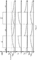
Figure 2 , where a time diagram representing different currents flowing incircuit 10 as a function of time t is shown, the command signal CMD has ON and OFF states which time length is controlled by thePWM controller 15. When the signal CMD is in the ON period, the load current ILOAD through thevalve 50 is increasing and corresponds to the a low side current ILS through thelow switch 12. When the signal CMD is in the OFF period, a so-called recirculation current, which corresponds to a high side current IHS through thehigh side switch 11, flows through thevalve 50 decreasing in value. Both the integrateddrivers current sensing circuit valve 50, in both the ON and OFF periods, i.e. the low side current ILS and the high side current IHS, with the exception of short time intervals, during the ON-OFF transitions. Thesensing circuit controller 15 receives as input a sensing current Isense that is the sum, performed in asum node 13, of the current sensed by the low and high side driver. Thecontroller 15 receives also as input a target current Itarget, which is set by the user or external control modules, which represents the set-point of thecontroller 15, and a PWM period TPWM. From the point of view of gthe control, thecontroller 15 uses the target current Itarget as the set-point, the sensing current Isense as the feedback quantity, and the error between the target current Itarget and the sensing current Isense feeds the proportional integral block, which in its turn feed the PWM block modulating the PWM period TPWM according to the value obtained by the proportional integral block. Therefore, thecircuit 10 allows to implement an accurate average current control, in a wide range of PWM periods and duty-cycle driving conditions. The availability of the load current measurement in almost all the PWM time period, allows to integrate a current control algorithm able to guarantee that the average load current Iload is regulated to match the target value Itarget with very good accuracy and independently from the real load current shape. Even if, applying the L-R series model for theload 50, the shape is different from the one ideally expected, the current is continuously measured by thesensing circuits module 15 in order to correctly control the real average value. - The draw-back of solutions like the one depicted in
Figure 1 is the cost of the controlling device, where two silicon area consuming power stages are needed, with the related current-sensing circuitry, which should have good matching characteristic, and three pins or terminals for each load, i.e. the terminals indicated as VB, OUT and PGND inFigure 1 . In modern ASIC devices, integrating a huge number of functions and drivers, pin count can be a limiting factor. - Solutions are also known which are less accurate than the one described with reference to
Figure 1 , but are suitable to specific automotive application, such as ABS Systems, where a great number of valves can be present and need to be driven, but not all of them require the same level of current control accuracy: depending on their purpose with respect to the hydraulic system, some of them can be simply ON-OFF driven or can be PWM driven with a less tight current control, i.e. the current control can implement a lower absolute current accuracy and/or the current can be measured/monitored only on a longer time period basis, i.e. not within a single PWM period. - To this regard, in
Figure 3 it is shown acircuit 20 for controlling the current in avalve 50 exemplary of such solutions implementing a less accurate control. Same reference number refers to component with the same function.Such circuit 20 for controlling the current in avalve 50 includes a integratedcircuit 20a, in particular an ASIC (Application Specific Integrated Circuit) and an externalrecirculating diode 22. Only the low-side integrateddriver sense circuitry 11b are present here, with two pins, node OUT and node PGND of theintegrated circuit 20a, needed to drive the load current Iload, while the recirculation current of thevalve 50 is driven by an external, i.e. external with respect to theintegrated circuit 20a, low-cost diode 22, which is connected between the output node OUT, i.e. the drain of thelow side switch 11, and the battery node VB, connected to battery voltage VBATT. - Therefore
such circuit 20 for controlling the current in avalve 50 can be regarded as including a pair of low side and a high side driving switches, which are however in this case obtained by a controllable switch, the low-side MOSFET switch 11, which is switched on to increase a load current flowing in theinductive load 50, and by therecirculation diode 22, which can be considered a high-side switch, although not switch controllable by a control signal, arranged to re-circulate the load current Iload when the controllable switch, i.e.MOSFET 11, is switched off. As mentioned before, therecirculation diode 22 is external with respect to the integratedcircuit 20a, this being a relevant feature as it reduces the cost of the integratedcircuit 20a. Therecirculation diode 22 is connected in parallel to theload 50, with the anode connected to the output node and the cathode connected to the battery voltage VBATT, so that when theMOSFET 11 is OFF, i.e. the switch is open, therecirculation diode 22 is direct conducting, recirculating the load current Iload flowing through the load toward the battery, while when theMOSFET 11 is ON, , i.e. the switch is closed, therecirculation diode 22 is inversely biased. - In such a circuital topology the load current Iload, when flowing through the
external recirculation diode 22 as diode current Idiode, since the low-side switch 11 is off and the low side current ILS is equal to zero, cannot be measured by the control circuit and therefore the real average current Ieverage with respect to the load current Iload cannot be measured, since only the low side current ILS is measurable. - Therefore, such a circuit it is operated as follows.
- The integrated
driver Figure 4 , receives a direct control command signal CMD signal from amicrocontroller 25, which is external with respect to theASIC 20a, on a input pin CN corresponding to the input node of thegate driver 11a, and sends back a current feedback If to themicrocontroller 25 via a SPI (Serial Parallel Interface) communication. The current feedback If is measured at half of the ON period, Ton, during the i+1-th cycle i+1. During each i-th PWM period, the ON period Ton is measured by the lessaccurate circuit 20 in ameasure module 28 and used to sample, by a sample and holdmodule 26, at the instant Toni/2 of the subsequent PWM cycle i+1, the load current Iload, to provide the current feedback value If, through an analog todigital converter 27, to themicrocontroller 25. Therefore, the subsequent PWM cycle i+1 is the contemporary measurement cycle, i.e. the real time cycle with respect to the loop operation, in which the load current is sensed, however the current feedback value If in this is calculated or measured using the cycle value of the previous PWM cycle i of ON time, Toni. Such current feedback value If differs from the real average current value flowing through thevalve 50, however this cannot be avoided, since the complete trend of the load current Iload is not available inside the integratedcircuit 20, if the OFF current is not measured to save costs. - There is therefore a trade-off between accuracy and costs. The current feedback If can be used by the
microcontroller 25 just to monitor the current or to implement a current control algorithm. Although a current-control algorithm operating on a PWM-period basis could be implemented, this would require quite a heavy SPI traffic load, that can be hardly sustained. Further, an important limitation for this driving topology is due to the very limited accuracy at low average currents: when a low average current is the target, a very small duty cycle has to be applied through the command signal CMD, limiting the period when the current can be sensed by thecircuit 20 to a very low percentage of the total period. This is made worse by the non-sensing intervals of thecurrent sense circuit 11b during the ON-OFF transitions of signal CMD, to guarantee that a reliable value can be provided as measured current, and, most important, by the non-linear behavior of thereal valve 50, that differs significantly from the "smooth" trend of a simple L-R series model. - Due to all the limitations described here above, the circuit arrangement shown in
figure 3 is limited to be used for valves requiring quite poor current control accuracy. - In view of the above, it is an objective of the present disclosure to provide solutions which overcome one or more of the above drawbacks.
- According to one or more embodiments, one or more of the above objectives is achieved by means of a circuit for controlling the current in inductive loads having the features specifically set forth in the claims that follow. Embodiments moreover concern a corresponding control method.
- The claims are an integral part of the technical teaching of the disclosure provided herein.
- As mentioned before, the present disclosure relates to Circuit for controlling the current in inductive loads, in particular electro-mechanical valves comprising a coil, comprising a driver circuit to drive a load current in said inductive load, said driver circuit including, in a integrated circuit portion of the driver circuit, a low side or high side driving switch obtained by a controllable switch, in particular a MOSFET, which is switched on to increase a load current flowing in the inductive load, and by a recirculation diode, external with respect to the integrated circuit portion of the driver circuit, arranged to re-circulate the load current when the controllable switch is switched off, said controlling circuit including a control module generating a control signal to switch on and off the controllable switch, wherein said control module includes a PWM (Pulse Width Modulation) current controller module, comprising a negative feedback closed loop comprising a module implementing at least a proportional control action and a integral control action feeding a PWM modulator module, said PWM current controller module receiving as feedback loop set-point a target current value and as feedback measured value of the loop an estimated value of the current flowing in the load during a measurement PWM cycle, said PWM current controller module being configured to generate said control signal for a control input of the controllable switch on the basis of an error between said target current and said estimate of the current flowing in the load.
- In various embodiments, the circuit includes that said controllable switch is a low side switch connected between an output node and a ground node and the recirculation diode is connected to a battery node, in parallel with respect to the inductive load.
- In various embodiments, the circuit includes that a sense circuit, in particular a sense amplifier, is connected to the switch to sense the load current and supply a sense current to a module performing said estimate of the current of the current flowing in the load.
- In various embodiments, the circuit includes that said estimate of the current flowing in the load is calculated as the half of the sum of a low current value acquired after the PWM current controller module issued a ON command signal for the switch and a high current value acquired before the end of the previous ON command signal.
- In various embodiments, the circuit includes that said module implementing at least a proportional control action and a integral control action implements also a derivative action.
- The solution refers also to a method for controlling the current in inductive loads, in particular electro-mechanical valves comprising a coil, comprising driving a load current in said inductive load by a pair of low side and a high side driving switches obtained by a controllable switch, in particular a MOSFET, which is switched on to increase a load current flowing in the inductive load , and by a recirculation diode arranged to re-circulate the load current when the controllable switch is switched off, generating a control signal to switch on and off the controllable switch, wherein said generating a control signal to switch on and off the controllable switch includes performing a PWM (Pulse Width Modulation) current control by a negative feedback closed loop, implementing at least a proportional control action and a integral control action and a PWM modulation, using as feedback loop set-point a target current value and as feedback measured value of the loop an estimated value of the current flowing in the load during a measurement PWM cycle, generating said control signal for a control input of the controllable switch on the basis of an error between said target current and said estimate of the current flowing in the load .
- In various embodiments, the method includes using as controllable switch a low side switch connected between an output node and a ground node and connecting the recirculation diode to a battery node , in parallel with respect to the inductive load .
- In various embodiments, the method includes sensing the current in the controllable switch to sense the load current and estimating on the basis of said sense current said estimated value of the current flowing in the load during a measurement PWM cycle .
- In various embodiments, the method includes that said estimating on the basis of said sense current said estimated value of the current flowing in the load during a measurement PWM cycle includes calculating as the half of the sum of a low current value acquired after the issuance of an ON command signal in the measurement PWM cycle and a high current value acquired just before or synchronously with the issuance of an OFF command signal.
- In various embodiments, the method includes that said low current value is acquired from the sense current after the issuance of an ON command signal in the measurement PWM cycle evaluating when the controllable switch closes, in particular after the settling of the sense current ,
said high current value is acquired just before or synchronously with the issuance of an OFF command signal evaluating when the controllable switch is open;
calculating a median current value, as the sum of the low current and the high current divided by two - In various embodiments, the method includes preventing sampling the high current value or low current value if the duty cycle of the PWM control signal is 100%.
- In various embodiments, the method includes that said module implementing at least a proportional control action and a integral control action implements also a derivative action.
- Embodiments of the present disclosure will now be described with reference to the annexed drawings, which are provided purely by way of non-limiting example and in which:
-
Figure 1 ,2 ,3 ,4 have been already described in the foregoing; -
Figure 5 shows schematically an embodiment of a control circuit of the type here described; -
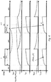
Figure 6 shows a time diagram representing currents and values used by the control circuit ofFigure 5 ; -
Figure 7 shows a flow diagram representing an embodiment of a method implemented by the circuit ofFigure 5 . - In the following description, numerous specific details are given to provide a thorough understanding of embodiments. The embodiments can be practiced without one or several specific details, or with other methods, components, materials, etc. In other instances, well-known structures, materials, or operations are not shown or described in detail to avoid obscuring aspects of the embodiments.
- Reference throughout this specification to "one embodiment" or "an embodiment" means that a particular feature, structure, or characteristic described in connection with the embodiment is included in at least one embodiment. Thus, the appearances of the phrases "in one embodiment" or "in an embodiment" in various places throughout this specification are not necessarily all referring to the same embodiment. Furthermore, the particular features, structures, or characteristics may be combined in any suitable manner in one or more embodiments.
- The headings provided herein are for convenience only and do not interpret the scope or meaning of the embodiments.
- In
figure 5 it is described a solution for controlling the current in inductive loads that obtains a sufficient accuracy and a real time current, using a single switch, in particular a low side switch represented by acurrent control circuit 30. Such a solution provides in thecurrent control circuit 30 a PWM current controller, configured to regulate the load current in real time, regulation in real time meaning regulation within a single PWM period, without requiring a high microprocessor work-load. A current feedback value for the PWM current controller to be compared with the target current value is extracted that minimizes the current error with respect to the real average current, taking in account also the real valve current shape. The solution here described uses anintegrated circuit 30a comprising an integrated current control loop with an external recirculation diode. Different possible control strategies are described to compute the feedback current value to be compared with target value, based on the available ON-current measurement. - As shown in
figure 5 , thecontrol circuit 30 presents substantially the same circuital arrangement of thecontrol circuit 20, having aintegrated circuit 30a including a singlelow side switch 11 having theload 50 connected between the output node OUT, which corresponds to the drain electrode of thelow side switch 11, the battery voltage VBATT. Therecirculation diode 22, external with respect to theintegrated circuit 30a, is connected between the same nodes, OUT and VBATT, to conduct directly the current into the battery node VBATT. - In this case, differently from the
circuit 20 shown infigure 2 , the command signal CMD is issued by thecontroller 15, which is included in acurrent controller module 35, included in theintegrated circuit 30a, which receives as one of its inputs the PWM period TPWM. The set-point input of thecontroller 15 however receives an error current Ierror computed as the difference, which is performed in aspecific sum module 31, also included in thecurrent controller module 35, between the target current Itarget and a median current Imid. Such median current Imid is measured in a mediancurrent extraction module 32, which receives the sense current Isense from thesense circuit 11b and the command signal CMD as inputs. - The
integrated circuit 30a therefore in the embodiment shown above in includes thecurrent controller module 35, thedriver current extraction module 32, thecurrent sensing circuit 11b. - With reference to
figure 6 , where it is shown a diagram of the current Isense as a function of time t, the median current Imid extracted by the mediancurrent extraction module 32 can be calculated on the basis of the the sense current Isense, corresponding to the low side current ILS, preferably as follows. A first PWM cycle, is defined from when the PWM control signal CMD goes from the OFF to the ON state, starting an ON period Toni, and from the subsequent OFF period Toffi. A subsequent PWM cycle i+1 is defined as measurement cycle, since, as better detailed during this cycle the median current Imid is calculated and feed to thenode 31 to calculate the error current Ierror updating the input of thecontroller 15, therefore varying the length of the on period Toni+1 of the measurement cycle i+1. - The median current Imid is obtained by computing an average value between a high current value Ihc measured when it occurs that the PWM control signal CMD goes from the ON to the OFF state, marking in
Figure 6 the beginning of the first PWM cycle i. The ON period Toni of the first PWM cycle i is shown with its area in hatched lines. A low current value Ilc is sampled or acquired when it occurs that the PWM control signal CMD goes from the OFF to the ON state at the end of the first PWM cycle i. The low current value Ilc of the current Isense is acquired as soon as theswitch 11 is fully ON and the current sense amplifier embodying thesense circuit 11b is settled to guarantee correct current measurement. The median current Imid is therefore obtained in the measurement cycle i+1, as soon as the low current value Ilc is measured at the beginning of the cycle i+1, averaging it with the high current Ihc which is read at the end of the cycle i using immediately the median current Imid to update thePI controller 15 computing the value of the ON time Toni+1 of the measurement cycle i+1 itself. - In
Figure 6 , where it shown a line corresponding to the average current value Iaverage, i.e. the real average value of the periodic current in the load, are indicated other quantities that can be computed by themodule 32 as median current Imid value. A possible choice is the average ON current value Iavgon, i.e the average value of the ON current, then another possible choice is the sense current value at Ton/2, I (Ton/2). - In typical driving conditions and with an RL series valve model, where the current ripple shape is very similar to a triangular wave (TON/TOFF ratio being lower than load time constant), these three alternative choices, the median current Imid, the average ON current value Iavgon, the sense current value at Ton/2, I(Ton/2), are almost equivalent, since all these three choices supply values that are very near to the true average current Iaverage. Current ripple measurements on a real valve installed in the complete application environment and driven at different target currents show a current ripple shape that is not fitting with the single time constant behavior provided by a simple R-L series model. In particular, the real current behavior shows a high slope as soon as the driver is turned on or off, while the current slope decreases as the on/off state is kept - it has to be fitted using therefore different time constants. The reason of this behavior seems to be the ferromagnetic characteristics of the valve core, with its hysteresis and saturation.
- Due to this non-linear behavior of the current ripple, the method based on the median current Imid provides the lowest error in in a wide target current range.
- It has to be underlined that in
figure 6 , for what concerns the median current Imid, with a point placed at half the OFF period of cycle i it is simply indicated indicated the value of the median current Imid on the vertical axis, so that such value of the median current Imid can be also graphically compared to the other estimates of the current and with respect to the average current Iaverage. However the median current Imid is computed at time t2 in the cycle i+1, and the solid line passing through the median current Imid point is just drawn to help the eye. - In
figure 7 it is shown a flow diagram representative of an embodiment of the specified method. - In a
step 110 thedriver circuit 30 is enabled. - In a
step 120 variable corresponding to the low current value Ilc and the high current value Ihc are initialized to the zero value. - In a
step 130 is evaluated if the command signal CMD is logic one, i.e. theswitch 11 is closed and the current ILS is passing through theload 50. In the negative, i.e. command signal CMD=0, control is brought backdownstream step 120, i.e. the method cycles around theevaluation step 130 till it the command signal CMD closes theswitch 11. - Therefore in the positive, a
step 140 of waiting for the settling of the sense current Isense after the switching on ofswitch 11 is performed. This can be performed by setting a settling time of thecurrent sense 11b. - After the
step 140, astep 150 of sampling the low current value Ilc is performed. - Then in a
step 160 is calculated the median current Imid value, in particular as the sum of the low current Ilc and the high current Ihc divided by two, i.e.
- In
such step 160, the updating of the median current Imid value includes updating the input corresponding to the error current Ierror of thecontroller 15, which determines the calculation of a new ON time TON for the PWM cycle taking place. - Then in a
step 170 is evaluated if the command signal CMD is logic zero, i.e. theswitch 11 is open and theload 50 current is no longer passing through the low-side driver. - In the affirmative the high current Ihc value is sampled in a
step 190 and control returnsdownstream step 120. Since the digital control is much faster than the low-side driver, the acquired or sampled value of high current Ihc is still the current in the load passing in the low-side driver 11, before this really enters an off state. The current value Ihc is acquired at the time instant during which the driver receives the control command CMD to go off, CMD=0. Such high current value Ihc thus is acquired just before or synchronously with the issuance of an OFF command signal evaluating when thecontrollable switch 11 is still close. - In the negative a
step 180 of evaluation of the duty cycle of the PWM signal is performed: if it is found that the duty cycle is 100%, then the high current Ihc value is sampled in astep 195 and control returnsdownstream step 120. The condition verified atstep 180, i.e. the duty-cycle of the PWM control signal CMD reaching 100% may occur for instance if the target current Itarget cannot be reached for some reason, or during a transient. Otherwise the high current Ihc value is not sampled and control returnsdownstream step 160 where the median current Imid value was calculated, waiting for high current Ihc sampling by CMD=0 or by PWM=100%. - Therefore, more in general the method here described provides generating at a
current controller module 35 the control signal CMD to switch on and off thecontrollable switch 11, includes performing a PWM (Pulse Width Modulation) current control by a negative feedback closed loop, implementing at least a proportional control action and a integral control action and a PWM modulation, using as feedback loop set-point the target current value Itarget and as feedback measured value of the loop an estimated value Imid of the current flowing in the load ILS during a measurement PWM cycle, generating said control signal CMD for the control input of thecontrollable switch 11 on the basis of the error current Ierror between said target current Itarget and said estimate Imid of the current ILS flowing in theload 50. In the preferred embodiment described with reference toFigure 5 the controllable switch is a low side switch. - As described with reference to
Figure 6 , the method includes sensing by thesense circuit 11b the current in thecontrollable switch 11 and estimating in themodule 32 on the basis of the sense current Isense the estimated value Imid of the current flowing in the load ILS during a measurement PWM cycle. Although alternate estimated values are possible, such as average ON current Iavgon or the sense current value at Ton/2, I(Ton/2), in a preferred embodiment, which allows real time control, the estimation atmodule 32 includes in general calculating as the half of the sum of a low current value Ilc acquired after the issuance of an ON command signal CMD in the measurement PWM cycle and a high current value Ihc acquired 170 just before or synchronously with the issuance of an OFF command signal. It is underlined that in preferably for the calculation of the median current Imid it is used a high current value Ihc acquired before the low current value Ilc. - In the embodiment specifically described with reference to
Figure 6 the low current value Ilc is acquired instep 130 from the sense current Isense after the issuance of an ON command signal CMD in the measurement PWM cycle evaluating when thecontrollable switch 11 becomes closed, in particular after the settling of the sense current Isense, the high current value Ihc is acquired in astep 170 before the end of the previous OFF command signal evaluating when thecontrollable switch 11 becomes open. Then instep 160 the median current Imid value is obtained as the sum of the low current Ilc and the high current Ihc divided by two. - It is underlined that if at
step 180 the duty-cycle is found to be 100%, in that PWM cycle the control signal CMD does not return to zero, i.e. the driver is not switched off. Therefore, at the end of the PWM cycle, both Ihc a Ilc are sampled at the same time, thus taking the same value. In the subsequent PWM cycle, starting immediately after this sampling operation, the value of the median current Imid is calculated as equal to the value of these two sample, and the error Ierror input of thecontroller 15 updated accordingly. - Therefore the solution here disclosed allows to implement a fully integrated real-time PWM controller for the inductive load, real time meaning that the controller is updated at each PWM cycle, with a latency lower that one PWM cycle. This solves therefore the problem that such a circuital topology in which the load current, when flowing through the external diode as diode current, since the low-side switch is off, cannot be measured by the control circuit and therefore the real average current with respect to the load current cannot be measured, since only the low side current is measurable.
- A real time current control loop of this type is faster to react to system variations (such as battery voltage change), to recover to the correct steady state average current value, in particular with respect to solution such as the one depicted in
figure 3 , where the current flowing in the load is read only occasionally. As discussed, implementing a current-control algorithm operating on a PWM-period basis in that context would require quite a heavy SPI traffic load and significant work-load for the microprocessor. - The above advantages are obtained in a low-cost driving topology, using an external recirculation diode, which, as indicated, however allows a real time current control, and, by the proportional integral control, allows a better current control accuracy at low target current values. The better current control accuracy is in particularly ensured by the use of the median current.
- Of course, without prejudice to the principle of the invention, the details of construction and the embodiments may vary widely with respect to what has been described and illustrated herein purely by way of example, without thereby departing from the scope of the present invention, as defined by the ensuing claims.
- In variant embodiments the controllable switch can be a high side switch and the recirculation diode connected accordingly to recirculate the current in the ground node.
Claims (12)
- Circuit for controlling the current in inductive loads, in particular electro-mechanical valves comprising a coil, comprising a driver circuit (20, 20a; 30) to drive a load current (Iload) in said inductive load (50), said driver circuit (20, 20a; 30) including, in an integrated circuit portion (20a) of the driver circuit (20, 20a; 30), a low side or high side driving switch (11, 22) obtained by a controllable switch (11), in particular a MOSFET, which is switched on to increase a load current flowing in the inductive load (50), and by a recirculation diode (22), external with respect to the integrated circuit portion (20a) of the driver circuit (20, 20a; 30), arranged to recirculate the load current (Iload) when the controllable switch is switched off, said controlling circuit including a control module (25; 35) generating a control signal (CMD) to switch on and off the controllable switch (11),
characterized in that
said control module (35) includes a PWM (Pulse Width Modulation) current controller module (35), comprising a negative feedback closed loop comprising a module implementing at least a proportional control action and a integral control action feeding a PWM modulator module (35), said PWM current controller module (35) receiving as feedback loop set-point a target current value (Itarget) and as feedback measured value of the loop an estimated value (Imid) of the current flowing in the load (ILS) during a measurement PWM cycle (i+1), said PWM current controller module (35) being configured to generate said control signal (CMD) for a control input of the controllable switch (11) on the basis of an error (Ierror) between said target current (Itarget) and said estimate (Imid) of the current (ILS) flowing in the load (50). - The circuit according to Claim 1, characterized in that said controllable switch (11) is a low side switch connected between an output node (OUT) and a ground node (PNGD) and the recirculation diode (22) is connected to a battery node (VBATT), in parallel with respect to the inductive load (50).
- The circuit according to Claim 1, characterized in that a sense circuit (11b), in particular a sense amplifier, is connected to the controllable switch (11) to sense the load current (ILS) and supply a sense current (Isense) to a module (32) performing said estimate of the current (Isense, Imid) of the current (ILS) flowing in the load (50).
- The circuit according to Claim 1, characterized in that said estimate (Isense, Imid) of the current (ILS). flowing in the load (50) is calculated as the half of the sum of a low current value (Ilc) acquired after the PWM current controller module (35) issues an ON command signal (CMD) for the controllable switch (11) and a high current value (Ihc) acquired before the end of the previous ON command signal.
- The circuit according to Claim 1, characterized in that said module implementing at least a proportional control action and an integral control action implements also a derivative action.
- A method for controlling the current in inductive loads, in particular electro-mechanical valves comprising a coil, comprising driving a load current (Iload) in said inductive load (50) by a pair of low side and a high side driving switches (11, 22) obtained by a controllable switch (11), in particular a MOSFET, which is switched on to increase a load current flowing in the inductive load (50), and by a recirculation diode (22) arranged to re-circulate the load current (Iload) when the controllable switch is switched off, generating (25; 35) a control signal (CMD) to switch on and off the controllable switch (11),
characterized in that
said generating (35) a control signal (CMD) to switch on and off the controllable switch (11) includes performing a PWM (Pulse Width Modulation) current control by a negative feedback closed loop, implementing at least a proportional control action and a integral control action and a PWM modulation, using as feedback loop set-point a target current value (Itarget) and as feedback measured value of the loop an estimated value (Isense, Imid) of the current flowing in the load (ILS) during a measurement PWM cycle (i+1), generating (35) said control signal (CMD) for a control input of the controllable switch (11) on the basis of an error (Ierror) between said target current (Itarget) and said estimate (Isense, Imid) of the current (ILS) flowing in the load (50). - The method according to Claim 6, characterized by using as controllable switch (11) a low side switch connected between an output node (OUT) and a ground node (PNGD) and connecting the recirculation diode (22) to a battery node (VBATT), in parallel with respect to the inductive load (50).
- The method according to Claim 6, characterized by sensing (11b) the current in the controllable switch (11) to sense the load current (ILS) and estimating (32) on the basis of said sense current (Isense) said estimated value (Imid) of the current flowing in the load (ILS) during a measurement PWM cycle (i+1).
- The method according to Claim 8, characterized in that said estimating (32) on the basis of said sense current (Isense) said estimated value (Imid) of the current flowing in the load (ILS) during a measurement PWM cycle (i+1) includes calculating as the half of the sum of a low current value (Ilc) acquired (130) after the issuance of an ON command signal (CMD) in the measurement PWM cycle (i+1) and a high current value (Ihc) acquired (170) just before or synchronously with the issuance of an OFF command signal.
- The method according to Claim 9, characterized in that said low current value (Ilc) is acquired (130) from the sense current (Isense) after the issuance of an ON command signal (CMD) in the measurement PWM cycle evaluating (130) when the controllable switch (11) closes, in particular after the settling of the sense current (Isense),
said high current value (Ihc) is acquired (170) acquired (170) just before or synchronously with the issuance of an OFF command signal evaluating (170) when the controllable switch (11) is still close.
calculating (160) a median current (Imid) value, as the sum of the low current (Ilc) and the high current (Ihc) divided by two. - The method according to Claim 9, characterized in that includes sampling the high current (Ihc) value and low current value (Ihc) at the end of a PWM period if the duty cycle of the PWM control signal (CMD) is 100%.
- The method according to any of the previous Claims from 6 to 11, characterized in that said negative feedback closed loop, implementing at least a proportional control action and a integral control action implements also a derivative action.
Applications Claiming Priority (1)
| Application Number | Priority Date | Filing Date | Title |
|---|---|---|---|
| IT102017000034070A IT201700034070A1 (en) | 2017-03-28 | 2017-03-28 | CURRENT CONTROL CIRCUIT IN INDUCTIVE LOADS AND RELATIVE CONTROL METHOD |
Publications (2)
| Publication Number | Publication Date |
|---|---|
| EP3382721A1 true EP3382721A1 (en) | 2018-10-03 |
| EP3382721B1 EP3382721B1 (en) | 2024-02-21 |
Family
ID=59521565
Family Applications (1)
| Application Number | Title | Priority Date | Filing Date |
|---|---|---|---|
| EP17191799.0A Active EP3382721B1 (en) | 2017-03-28 | 2017-09-19 | Circuit for controlling the current in inductive loads and control method therefor |
Country Status (3)
| Country | Link |
|---|---|
| US (1) | US10982785B2 (en) |
| EP (1) | EP3382721B1 (en) |
| IT (1) | IT201700034070A1 (en) |
Cited By (1)
| Publication number | Priority date | Publication date | Assignee | Title |
|---|---|---|---|---|
| CN111664289A (en) * | 2020-06-01 | 2020-09-15 | 浙江工业大学 | Method for controlling opening and closing process of hydraulic valve through database and pulse width modulation |
Families Citing this family (2)
| Publication number | Priority date | Publication date | Assignee | Title |
|---|---|---|---|---|
| US10784917B2 (en) * | 2018-11-27 | 2020-09-22 | Texas Instruments Incorporated | PSI5 base current sampling in synchronous mode |
| EP4720552A4 (en) * | 2023-05-24 | 2026-05-20 | Siemens Healthcare Diagnostics Inc | Electromechanical PWM valve driver with two-way current feedback |
Citations (3)
| Publication number | Priority date | Publication date | Assignee | Title |
|---|---|---|---|---|
| US7235946B2 (en) * | 2005-01-12 | 2007-06-26 | Mando Corporation | Actuator current control method |
| US20090085544A1 (en) * | 2007-09-28 | 2009-04-02 | Infineon Technologies Ag | Current regulator and method for regulating current |
| US7872845B2 (en) * | 2007-03-30 | 2011-01-18 | Infineon Technologies Ag | Control system |
Family Cites Families (4)
| Publication number | Priority date | Publication date | Assignee | Title |
|---|---|---|---|---|
| EP1381060A4 (en) * | 2001-04-20 | 2010-03-10 | Sanken Electric Co Ltd | Solenoid drive apparatus and drive method |
| US6979987B2 (en) * | 2002-11-14 | 2005-12-27 | Fyre Storm, Inc. | Method of regulating an output voltage of a power converter by sensing the output voltage during a first time interval and calculating a next current value in an inductor sufficient to bring the output voltage to a target voltage within a second time interval immediately following the first time interval and varying a duty cycle of a switch during the second time interval |
| JP4359855B2 (en) * | 2007-07-09 | 2009-11-11 | Smc株式会社 | Solenoid valve drive circuit and solenoid valve |
| JP5978932B2 (en) * | 2012-11-07 | 2016-08-24 | 株式会社デンソー | Inductive load controller |
-
2017
- 2017-03-28 IT IT102017000034070A patent/IT201700034070A1/en unknown
- 2017-09-19 EP EP17191799.0A patent/EP3382721B1/en active Active
- 2017-10-25 US US15/793,464 patent/US10982785B2/en active Active
Patent Citations (3)
| Publication number | Priority date | Publication date | Assignee | Title |
|---|---|---|---|---|
| US7235946B2 (en) * | 2005-01-12 | 2007-06-26 | Mando Corporation | Actuator current control method |
| US7872845B2 (en) * | 2007-03-30 | 2011-01-18 | Infineon Technologies Ag | Control system |
| US20090085544A1 (en) * | 2007-09-28 | 2009-04-02 | Infineon Technologies Ag | Current regulator and method for regulating current |
Cited By (1)
| Publication number | Priority date | Publication date | Assignee | Title |
|---|---|---|---|---|
| CN111664289A (en) * | 2020-06-01 | 2020-09-15 | 浙江工业大学 | Method for controlling opening and closing process of hydraulic valve through database and pulse width modulation |
Also Published As
| Publication number | Publication date |
|---|---|
| US10982785B2 (en) | 2021-04-20 |
| EP3382721B1 (en) | 2024-02-21 |
| IT201700034070A1 (en) | 2018-09-28 |
| US20180283570A1 (en) | 2018-10-04 |
Similar Documents
| Publication | Publication Date | Title |
|---|---|---|
| US8482211B2 (en) | Circuit for the operation of at least one LED | |
| US8400798B2 (en) | Predictive current control in driving a load in a PWM mode | |
| US8143870B2 (en) | Methods and apparatus for current sensing | |
| US10476391B2 (en) | Voltage converting device | |
| CN105281571B (en) | For the controllable conduction time reduction with the regulator of PFM mode operations | |
| EP3382721B1 (en) | Circuit for controlling the current in inductive loads and control method therefor | |
| US8866464B2 (en) | Systems and methods for real time current sense for a switching converter | |
| US9973084B2 (en) | Switching voltage regulator input power estimation | |
| US9203304B2 (en) | Switching regulator | |
| WO2012041308A1 (en) | Method and device for determining the state of an electrically controlled valve | |
| CN101667776A (en) | System and method for reducing voltage overshoot during load release within a buck regulator | |
| US9124175B2 (en) | Load drive control device | |
| CN107408884B (en) | Power conversion device and control method for power conversion device | |
| DE102012201383B4 (en) | Uc-based power source | |
| US7683590B2 (en) | Step-down switching DC-DC converter | |
| CN113853736B (en) | Current control device | |
| TWI403874B (en) | Current control systems and methods with current feedbacks | |
| EP1617549A2 (en) | DC/DC converter employing synchronous rectification | |
| JP2019176651A (en) | On-vehicle dcdc converter | |
| US10270373B2 (en) | Method for controlling the current of an inductive load | |
| US8836299B2 (en) | Voltage converter | |
| CN106464136B (en) | switching power supply | |
| US9985544B2 (en) | Electronic switch | |
| JP2010199438A (en) | Solenoid driving device, and brake device | |
| KR101230547B1 (en) | Apparatus for controlling pulse width modulation and method for controlling thereof |
Legal Events
| Date | Code | Title | Description |
|---|---|---|---|
| PUAI | Public reference made under article 153(3) epc to a published international application that has entered the european phase |
Free format text: ORIGINAL CODE: 0009012 |
|
| STAA | Information on the status of an ep patent application or granted ep patent |
Free format text: STATUS: THE APPLICATION HAS BEEN PUBLISHED |
|
| AK | Designated contracting states |
Kind code of ref document: A1 Designated state(s): AL AT BE BG CH CY CZ DE DK EE ES FI FR GB GR HR HU IE IS IT LI LT LU LV MC MK MT NL NO PL PT RO RS SE SI SK SM TR |
|
| AX | Request for extension of the european patent |
Extension state: BA ME |
|
| STAA | Information on the status of an ep patent application or granted ep patent |
Free format text: STATUS: REQUEST FOR EXAMINATION WAS MADE |
|
| 17P | Request for examination filed |
Effective date: 20190402 |
|
| RBV | Designated contracting states (corrected) |
Designated state(s): AL AT BE BG CH CY CZ DE DK EE ES FI FR GB GR HR HU IE IS IT LI LT LU LV MC MK MT NL NO PL PT RO RS SE SI SK SM TR |
|
| STAA | Information on the status of an ep patent application or granted ep patent |
Free format text: STATUS: EXAMINATION IS IN PROGRESS |
|
| 17Q | First examination report despatched |
Effective date: 20210218 |
|
| RIC1 | Information provided on ipc code assigned before grant |
Ipc: H03K 7/08 20060101ALI20230904BHEP Ipc: H01H 47/32 20060101ALI20230904BHEP Ipc: H01F 7/18 20060101AFI20230904BHEP |
|
| GRAP | Despatch of communication of intention to grant a patent |
Free format text: ORIGINAL CODE: EPIDOSNIGR1 |
|
| STAA | Information on the status of an ep patent application or granted ep patent |
Free format text: STATUS: GRANT OF PATENT IS INTENDED |
|
| INTG | Intention to grant announced |
Effective date: 20231013 |
|
| GRAS | Grant fee paid |
Free format text: ORIGINAL CODE: EPIDOSNIGR3 |
|
| GRAA | (expected) grant |
Free format text: ORIGINAL CODE: 0009210 |
|
| STAA | Information on the status of an ep patent application or granted ep patent |
Free format text: STATUS: THE PATENT HAS BEEN GRANTED |
|
| AK | Designated contracting states |
Kind code of ref document: B1 Designated state(s): AL AT BE BG CH CY CZ DE DK EE ES FI FR GB GR HR HU IE IS IT LI LT LU LV MC MK MT NL NO PL PT RO RS SE SI SK SM TR |
|
| REG | Reference to a national code |
Ref country code: GB Ref legal event code: FG4D |
|
| REG | Reference to a national code |
Ref country code: CH Ref legal event code: EP |
|
| REG | Reference to a national code |
Ref country code: DE Ref legal event code: R096 Ref document number: 602017079303 Country of ref document: DE |
|
| REG | Reference to a national code |
Ref country code: IE Ref legal event code: FG4D |
|
| REG | Reference to a national code |
Ref country code: LT Ref legal event code: MG9D |
|
| REG | Reference to a national code |
Ref country code: NL Ref legal event code: MP Effective date: 20240221 |
|
| PG25 | Lapsed in a contracting state [announced via postgrant information from national office to epo] |
Ref country code: IS Free format text: LAPSE BECAUSE OF FAILURE TO SUBMIT A TRANSLATION OF THE DESCRIPTION OR TO PAY THE FEE WITHIN THE PRESCRIBED TIME-LIMIT Effective date: 20240621 |
|
| PG25 | Lapsed in a contracting state [announced via postgrant information from national office to epo] |
Ref country code: LT Free format text: LAPSE BECAUSE OF FAILURE TO SUBMIT A TRANSLATION OF THE DESCRIPTION OR TO PAY THE FEE WITHIN THE PRESCRIBED TIME-LIMIT Effective date: 20240221 |
|
| PG25 | Lapsed in a contracting state [announced via postgrant information from national office to epo] |
Ref country code: GR Free format text: LAPSE BECAUSE OF FAILURE TO SUBMIT A TRANSLATION OF THE DESCRIPTION OR TO PAY THE FEE WITHIN THE PRESCRIBED TIME-LIMIT Effective date: 20240522 |
|
| REG | Reference to a national code |
Ref country code: AT Ref legal event code: MK05 Ref document number: 1659841 Country of ref document: AT Kind code of ref document: T Effective date: 20240221 |
|
| PG25 | Lapsed in a contracting state [announced via postgrant information from national office to epo] |
Ref country code: NL Free format text: LAPSE BECAUSE OF FAILURE TO SUBMIT A TRANSLATION OF THE DESCRIPTION OR TO PAY THE FEE WITHIN THE PRESCRIBED TIME-LIMIT Effective date: 20240221 Ref country code: RS Free format text: LAPSE BECAUSE OF FAILURE TO SUBMIT A TRANSLATION OF THE DESCRIPTION OR TO PAY THE FEE WITHIN THE PRESCRIBED TIME-LIMIT Effective date: 20240521 Ref country code: HR Free format text: LAPSE BECAUSE OF FAILURE TO SUBMIT A TRANSLATION OF THE DESCRIPTION OR TO PAY THE FEE WITHIN THE PRESCRIBED TIME-LIMIT Effective date: 20240221 |
|
| PG25 | Lapsed in a contracting state [announced via postgrant information from national office to epo] |
Ref country code: ES Free format text: LAPSE BECAUSE OF FAILURE TO SUBMIT A TRANSLATION OF THE DESCRIPTION OR TO PAY THE FEE WITHIN THE PRESCRIBED TIME-LIMIT Effective date: 20240221 |
|
| PG25 | Lapsed in a contracting state [announced via postgrant information from national office to epo] |
Ref country code: AT Free format text: LAPSE BECAUSE OF FAILURE TO SUBMIT A TRANSLATION OF THE DESCRIPTION OR TO PAY THE FEE WITHIN THE PRESCRIBED TIME-LIMIT Effective date: 20240221 |
|
| PG25 | Lapsed in a contracting state [announced via postgrant information from national office to epo] |
Ref country code: RS Free format text: LAPSE BECAUSE OF FAILURE TO SUBMIT A TRANSLATION OF THE DESCRIPTION OR TO PAY THE FEE WITHIN THE PRESCRIBED TIME-LIMIT Effective date: 20240521 Ref country code: NO Free format text: LAPSE BECAUSE OF FAILURE TO SUBMIT A TRANSLATION OF THE DESCRIPTION OR TO PAY THE FEE WITHIN THE PRESCRIBED TIME-LIMIT Effective date: 20240521 Ref country code: NL Free format text: LAPSE BECAUSE OF FAILURE TO SUBMIT A TRANSLATION OF THE DESCRIPTION OR TO PAY THE FEE WITHIN THE PRESCRIBED TIME-LIMIT Effective date: 20240221 Ref country code: LT Free format text: LAPSE BECAUSE OF FAILURE TO SUBMIT A TRANSLATION OF THE DESCRIPTION OR TO PAY THE FEE WITHIN THE PRESCRIBED TIME-LIMIT Effective date: 20240221 Ref country code: IS Free format text: LAPSE BECAUSE OF FAILURE TO SUBMIT A TRANSLATION OF THE DESCRIPTION OR TO PAY THE FEE WITHIN THE PRESCRIBED TIME-LIMIT Effective date: 20240621 Ref country code: HR Free format text: LAPSE BECAUSE OF FAILURE TO SUBMIT A TRANSLATION OF THE DESCRIPTION OR TO PAY THE FEE WITHIN THE PRESCRIBED TIME-LIMIT Effective date: 20240221 Ref country code: GR Free format text: LAPSE BECAUSE OF FAILURE TO SUBMIT A TRANSLATION OF THE DESCRIPTION OR TO PAY THE FEE WITHIN THE PRESCRIBED TIME-LIMIT Effective date: 20240522 Ref country code: FI Free format text: LAPSE BECAUSE OF FAILURE TO SUBMIT A TRANSLATION OF THE DESCRIPTION OR TO PAY THE FEE WITHIN THE PRESCRIBED TIME-LIMIT Effective date: 20240221 Ref country code: ES Free format text: LAPSE BECAUSE OF FAILURE TO SUBMIT A TRANSLATION OF THE DESCRIPTION OR TO PAY THE FEE WITHIN THE PRESCRIBED TIME-LIMIT Effective date: 20240221 Ref country code: BG Free format text: LAPSE BECAUSE OF FAILURE TO SUBMIT A TRANSLATION OF THE DESCRIPTION OR TO PAY THE FEE WITHIN THE PRESCRIBED TIME-LIMIT Effective date: 20240221 Ref country code: AT Free format text: LAPSE BECAUSE OF FAILURE TO SUBMIT A TRANSLATION OF THE DESCRIPTION OR TO PAY THE FEE WITHIN THE PRESCRIBED TIME-LIMIT Effective date: 20240221 |
|
| PG25 | Lapsed in a contracting state [announced via postgrant information from national office to epo] |
Ref country code: PL Free format text: LAPSE BECAUSE OF FAILURE TO SUBMIT A TRANSLATION OF THE DESCRIPTION OR TO PAY THE FEE WITHIN THE PRESCRIBED TIME-LIMIT Effective date: 20240221 Ref country code: PT Free format text: LAPSE BECAUSE OF FAILURE TO SUBMIT A TRANSLATION OF THE DESCRIPTION OR TO PAY THE FEE WITHIN THE PRESCRIBED TIME-LIMIT Effective date: 20240621 |
|
| PG25 | Lapsed in a contracting state [announced via postgrant information from national office to epo] |
Ref country code: SE Free format text: LAPSE BECAUSE OF FAILURE TO SUBMIT A TRANSLATION OF THE DESCRIPTION OR TO PAY THE FEE WITHIN THE PRESCRIBED TIME-LIMIT Effective date: 20240221 Ref country code: PT Free format text: LAPSE BECAUSE OF FAILURE TO SUBMIT A TRANSLATION OF THE DESCRIPTION OR TO PAY THE FEE WITHIN THE PRESCRIBED TIME-LIMIT Effective date: 20240621 Ref country code: PL Free format text: LAPSE BECAUSE OF FAILURE TO SUBMIT A TRANSLATION OF THE DESCRIPTION OR TO PAY THE FEE WITHIN THE PRESCRIBED TIME-LIMIT Effective date: 20240221 Ref country code: LV Free format text: LAPSE BECAUSE OF FAILURE TO SUBMIT A TRANSLATION OF THE DESCRIPTION OR TO PAY THE FEE WITHIN THE PRESCRIBED TIME-LIMIT Effective date: 20240221 |
|
| PG25 | Lapsed in a contracting state [announced via postgrant information from national office to epo] |
Ref country code: DK Free format text: LAPSE BECAUSE OF FAILURE TO SUBMIT A TRANSLATION OF THE DESCRIPTION OR TO PAY THE FEE WITHIN THE PRESCRIBED TIME-LIMIT Effective date: 20240221 |
|
| PG25 | Lapsed in a contracting state [announced via postgrant information from national office to epo] |
Ref country code: SM Free format text: LAPSE BECAUSE OF FAILURE TO SUBMIT A TRANSLATION OF THE DESCRIPTION OR TO PAY THE FEE WITHIN THE PRESCRIBED TIME-LIMIT Effective date: 20240221 |
|
| PG25 | Lapsed in a contracting state [announced via postgrant information from national office to epo] |
Ref country code: CZ Free format text: LAPSE BECAUSE OF FAILURE TO SUBMIT A TRANSLATION OF THE DESCRIPTION OR TO PAY THE FEE WITHIN THE PRESCRIBED TIME-LIMIT Effective date: 20240221 Ref country code: EE Free format text: LAPSE BECAUSE OF FAILURE TO SUBMIT A TRANSLATION OF THE DESCRIPTION OR TO PAY THE FEE WITHIN THE PRESCRIBED TIME-LIMIT Effective date: 20240221 |
|
| PG25 | Lapsed in a contracting state [announced via postgrant information from national office to epo] |
Ref country code: SK Free format text: LAPSE BECAUSE OF FAILURE TO SUBMIT A TRANSLATION OF THE DESCRIPTION OR TO PAY THE FEE WITHIN THE PRESCRIBED TIME-LIMIT Effective date: 20240221 |
|
| PG25 | Lapsed in a contracting state [announced via postgrant information from national office to epo] |
Ref country code: SM Free format text: LAPSE BECAUSE OF FAILURE TO SUBMIT A TRANSLATION OF THE DESCRIPTION OR TO PAY THE FEE WITHIN THE PRESCRIBED TIME-LIMIT Effective date: 20240221 Ref country code: SK Free format text: LAPSE BECAUSE OF FAILURE TO SUBMIT A TRANSLATION OF THE DESCRIPTION OR TO PAY THE FEE WITHIN THE PRESCRIBED TIME-LIMIT Effective date: 20240221 Ref country code: RO Free format text: LAPSE BECAUSE OF FAILURE TO SUBMIT A TRANSLATION OF THE DESCRIPTION OR TO PAY THE FEE WITHIN THE PRESCRIBED TIME-LIMIT Effective date: 20240221 Ref country code: EE Free format text: LAPSE BECAUSE OF FAILURE TO SUBMIT A TRANSLATION OF THE DESCRIPTION OR TO PAY THE FEE WITHIN THE PRESCRIBED TIME-LIMIT Effective date: 20240221 Ref country code: DK Free format text: LAPSE BECAUSE OF FAILURE TO SUBMIT A TRANSLATION OF THE DESCRIPTION OR TO PAY THE FEE WITHIN THE PRESCRIBED TIME-LIMIT Effective date: 20240221 Ref country code: CZ Free format text: LAPSE BECAUSE OF FAILURE TO SUBMIT A TRANSLATION OF THE DESCRIPTION OR TO PAY THE FEE WITHIN THE PRESCRIBED TIME-LIMIT Effective date: 20240221 |
|
| REG | Reference to a national code |
Ref country code: DE Ref legal event code: R097 Ref document number: 602017079303 Country of ref document: DE |
|
| PG25 | Lapsed in a contracting state [announced via postgrant information from national office to epo] |
Ref country code: IT Free format text: LAPSE BECAUSE OF FAILURE TO SUBMIT A TRANSLATION OF THE DESCRIPTION OR TO PAY THE FEE WITHIN THE PRESCRIBED TIME-LIMIT Effective date: 20240221 |
|
| PLBE | No opposition filed within time limit |
Free format text: ORIGINAL CODE: 0009261 |
|
| STAA | Information on the status of an ep patent application or granted ep patent |
Free format text: STATUS: NO OPPOSITION FILED WITHIN TIME LIMIT |
|
| PG25 | Lapsed in a contracting state [announced via postgrant information from national office to epo] |
Ref country code: IT Free format text: LAPSE BECAUSE OF FAILURE TO SUBMIT A TRANSLATION OF THE DESCRIPTION OR TO PAY THE FEE WITHIN THE PRESCRIBED TIME-LIMIT Effective date: 20240221 |
|
| 26N | No opposition filed |
Effective date: 20241122 |
|
| PG25 | Lapsed in a contracting state [announced via postgrant information from national office to epo] |
Ref country code: SI Free format text: LAPSE BECAUSE OF FAILURE TO SUBMIT A TRANSLATION OF THE DESCRIPTION OR TO PAY THE FEE WITHIN THE PRESCRIBED TIME-LIMIT Effective date: 20240221 Ref country code: MC Free format text: LAPSE BECAUSE OF FAILURE TO SUBMIT A TRANSLATION OF THE DESCRIPTION OR TO PAY THE FEE WITHIN THE PRESCRIBED TIME-LIMIT Effective date: 20240221 |
|
| REG | Reference to a national code |
Ref country code: CH Ref legal event code: PL |
|
| PG25 | Lapsed in a contracting state [announced via postgrant information from national office to epo] |
Ref country code: LU Free format text: LAPSE BECAUSE OF NON-PAYMENT OF DUE FEES Effective date: 20240919 |
|
| GBPC | Gb: european patent ceased through non-payment of renewal fee |
Effective date: 20240919 |
|
| PG25 | Lapsed in a contracting state [announced via postgrant information from national office to epo] |
Ref country code: GB Free format text: LAPSE BECAUSE OF NON-PAYMENT OF DUE FEES Effective date: 20240919 |
|
| REG | Reference to a national code |
Ref country code: BE Ref legal event code: MM Effective date: 20240930 |
|
| PG25 | Lapsed in a contracting state [announced via postgrant information from national office to epo] |
Ref country code: BE Free format text: LAPSE BECAUSE OF NON-PAYMENT OF DUE FEES Effective date: 20240930 |
|
| PG25 | Lapsed in a contracting state [announced via postgrant information from national office to epo] |
Ref country code: FR Free format text: LAPSE BECAUSE OF NON-PAYMENT OF DUE FEES Effective date: 20240930 |
|
| PG25 | Lapsed in a contracting state [announced via postgrant information from national office to epo] |
Ref country code: CH Free format text: LAPSE BECAUSE OF NON-PAYMENT OF DUE FEES Effective date: 20240930 |
|
| PG25 | Lapsed in a contracting state [announced via postgrant information from national office to epo] |
Ref country code: IE Free format text: LAPSE BECAUSE OF NON-PAYMENT OF DUE FEES Effective date: 20240919 |
|
| PGFP | Annual fee paid to national office [announced via postgrant information from national office to epo] |
Ref country code: DE Payment date: 20250820 Year of fee payment: 9 |
|
| PG25 | Lapsed in a contracting state [announced via postgrant information from national office to epo] |
Ref country code: CY Free format text: LAPSE BECAUSE OF FAILURE TO SUBMIT A TRANSLATION OF THE DESCRIPTION OR TO PAY THE FEE WITHIN THE PRESCRIBED TIME-LIMIT; INVALID AB INITIO Effective date: 20170919 |
|
| PG25 | Lapsed in a contracting state [announced via postgrant information from national office to epo] |
Ref country code: HU Free format text: LAPSE BECAUSE OF FAILURE TO SUBMIT A TRANSLATION OF THE DESCRIPTION OR TO PAY THE FEE WITHIN THE PRESCRIBED TIME-LIMIT; INVALID AB INITIO Effective date: 20170919 |