EP3374849B1 - Processing signals from a touchscreen panel - Google Patents
Processing signals from a touchscreen panel Download PDFInfo
- Publication number
- EP3374849B1 EP3374849B1 EP16797600.0A EP16797600A EP3374849B1 EP 3374849 B1 EP3374849 B1 EP 3374849B1 EP 16797600 A EP16797600 A EP 16797600A EP 3374849 B1 EP3374849 B1 EP 3374849B1
- Authority
- EP
- European Patent Office
- Prior art keywords
- array
- touch
- noise
- values
- signal
- Prior art date
- Legal status (The legal status is an assumption and is not a legal conclusion. Google has not performed a legal analysis and makes no representation as to the accuracy of the status listed.)
- Active
Links
Images









Classifications
-
- G—PHYSICS
- G06—COMPUTING OR CALCULATING; COUNTING
- G06F—ELECTRIC DIGITAL DATA PROCESSING
- G06F3/00—Input arrangements for transferring data to be processed into a form capable of being handled by the computer; Output arrangements for transferring data from processing unit to output unit, e.g. interface arrangements
- G06F3/01—Input arrangements or combined input and output arrangements for interaction between user and computer
- G06F3/03—Arrangements for converting the position or the displacement of a member into a coded form
- G06F3/041—Digitisers, e.g. for touch screens or touch pads, characterised by the transducing means
- G06F3/0416—Control or interface arrangements specially adapted for digitisers
- G06F3/0418—Control or interface arrangements specially adapted for digitisers for error correction or compensation, e.g. based on parallax, calibration or alignment
-
- G—PHYSICS
- G06—COMPUTING OR CALCULATING; COUNTING
- G06F—ELECTRIC DIGITAL DATA PROCESSING
- G06F3/00—Input arrangements for transferring data to be processed into a form capable of being handled by the computer; Output arrangements for transferring data from processing unit to output unit, e.g. interface arrangements
- G06F3/01—Input arrangements or combined input and output arrangements for interaction between user and computer
- G06F3/03—Arrangements for converting the position or the displacement of a member into a coded form
- G06F3/041—Digitisers, e.g. for touch screens or touch pads, characterised by the transducing means
- G06F3/044—Digitisers, e.g. for touch screens or touch pads, characterised by the transducing means by capacitive means
- G06F3/0443—Digitisers, e.g. for touch screens or touch pads, characterised by the transducing means by capacitive means using a single layer of sensing electrodes
-
- G—PHYSICS
- G06—COMPUTING OR CALCULATING; COUNTING
- G06F—ELECTRIC DIGITAL DATA PROCESSING
- G06F3/00—Input arrangements for transferring data to be processed into a form capable of being handled by the computer; Output arrangements for transferring data from processing unit to output unit, e.g. interface arrangements
- G06F3/01—Input arrangements or combined input and output arrangements for interaction between user and computer
- G06F3/03—Arrangements for converting the position or the displacement of a member into a coded form
- G06F3/041—Digitisers, e.g. for touch screens or touch pads, characterised by the transducing means
- G06F3/0416—Control or interface arrangements specially adapted for digitisers
- G06F3/0418—Control or interface arrangements specially adapted for digitisers for error correction or compensation, e.g. based on parallax, calibration or alignment
- G06F3/04182—Filtering of noise external to the device and not generated by digitiser components
-
- G—PHYSICS
- G06—COMPUTING OR CALCULATING; COUNTING
- G06F—ELECTRIC DIGITAL DATA PROCESSING
- G06F3/00—Input arrangements for transferring data to be processed into a form capable of being handled by the computer; Output arrangements for transferring data from processing unit to output unit, e.g. interface arrangements
- G06F3/01—Input arrangements or combined input and output arrangements for interaction between user and computer
- G06F3/03—Arrangements for converting the position or the displacement of a member into a coded form
- G06F3/041—Digitisers, e.g. for touch screens or touch pads, characterised by the transducing means
- G06F3/0416—Control or interface arrangements specially adapted for digitisers
- G06F3/0418—Control or interface arrangements specially adapted for digitisers for error correction or compensation, e.g. based on parallax, calibration or alignment
- G06F3/04184—Synchronisation with the driving of the display or the backlighting unit to avoid interferences generated internally
-
- G—PHYSICS
- G06—COMPUTING OR CALCULATING; COUNTING
- G06F—ELECTRIC DIGITAL DATA PROCESSING
- G06F3/00—Input arrangements for transferring data to be processed into a form capable of being handled by the computer; Output arrangements for transferring data from processing unit to output unit, e.g. interface arrangements
- G06F3/01—Input arrangements or combined input and output arrangements for interaction between user and computer
- G06F3/03—Arrangements for converting the position or the displacement of a member into a coded form
- G06F3/041—Digitisers, e.g. for touch screens or touch pads, characterised by the transducing means
- G06F3/044—Digitisers, e.g. for touch screens or touch pads, characterised by the transducing means by capacitive means
- G06F3/0445—Digitisers, e.g. for touch screens or touch pads, characterised by the transducing means by capacitive means using two or more layers of sensing electrodes, e.g. using two layers of electrodes separated by a dielectric layer
-
- G—PHYSICS
- G06—COMPUTING OR CALCULATING; COUNTING
- G06F—ELECTRIC DIGITAL DATA PROCESSING
- G06F3/00—Input arrangements for transferring data to be processed into a form capable of being handled by the computer; Output arrangements for transferring data from processing unit to output unit, e.g. interface arrangements
- G06F3/01—Input arrangements or combined input and output arrangements for interaction between user and computer
- G06F3/03—Arrangements for converting the position or the displacement of a member into a coded form
- G06F3/041—Digitisers, e.g. for touch screens or touch pads, characterised by the transducing means
- G06F3/044—Digitisers, e.g. for touch screens or touch pads, characterised by the transducing means by capacitive means
- G06F3/0446—Digitisers, e.g. for touch screens or touch pads, characterised by the transducing means by capacitive means using a grid-like structure of electrodes in at least two directions, e.g. using row and column electrodes
-
- G—PHYSICS
- G06—COMPUTING OR CALCULATING; COUNTING
- G06T—IMAGE DATA PROCESSING OR GENERATION, IN GENERAL
- G06T5/00—Image enhancement or restoration
- G06T5/70—Denoising; Smoothing
-
- G—PHYSICS
- G06—COMPUTING OR CALCULATING; COUNTING
- G06V—IMAGE OR VIDEO RECOGNITION OR UNDERSTANDING
- G06V10/00—Arrangements for image or video recognition or understanding
- G06V10/20—Image preprocessing
- G06V10/26—Segmentation of patterns in the image field; Cutting or merging of image elements to establish the pattern region, e.g. clustering-based techniques; Detection of occlusion
-
- G—PHYSICS
- G06—COMPUTING OR CALCULATING; COUNTING
- G06V—IMAGE OR VIDEO RECOGNITION OR UNDERSTANDING
- G06V10/00—Arrangements for image or video recognition or understanding
- G06V10/20—Image preprocessing
- G06V10/30—Noise filtering
-
- H—ELECTRICITY
- H04—ELECTRIC COMMUNICATION TECHNIQUE
- H04N—PICTORIAL COMMUNICATION, e.g. TELEVISION
- H04N25/00—Circuitry of solid-state image sensors [SSIS]; Control thereof
- H04N25/60—Noise processing, e.g. detecting, correcting, reducing or removing noise
- H04N25/616—Noise processing, e.g. detecting, correcting, reducing or removing noise involving a correlated sampling function, e.g. correlated double sampling [CDS] or triple sampling
-
- G—PHYSICS
- G06—COMPUTING OR CALCULATING; COUNTING
- G06F—ELECTRIC DIGITAL DATA PROCESSING
- G06F2203/00—Indexing scheme relating to G06F3/00 - G06F3/048
- G06F2203/041—Indexing scheme relating to G06F3/041 - G06F3/045
- G06F2203/04104—Multi-touch detection in digitiser, i.e. details about the simultaneous detection of a plurality of touching locations, e.g. multiple fingers or pen and finger
Definitions
- the present invention relates to processing signals from a touchscreen panel.
- Touchscreen panels are widely used in consumer electronic devices. Resistive and capacitive touchscreen panels have widely adopted as input means for data processing devices, in particular for mobile devices such as smartphones, tablet computers and laptops. There is also growing interest in pressure sensing touchscreen panels, for example as described in US 2014/0008203 A1 .
- mis-registration of user input is undesirable. For example, mis-registration of the presence or location of a user's interaction using a digit or stylus.
- Two of the main factors which influence touch registration and power consumption are noise and multi-valued offsets in the output signals from a touchscreen panel.
- Touchscreen panels are commonly arranged to record user interactions or touch events in a two dimensional grid or array arrangement.
- touch event refers to a user interacting with a touchscreen by touching or pressing the touchscreen panel using a digit/finger or a suitable stylus.
- the signals output from a touchscreen panel having a two dimensional grid or array arrangement are collated into a corresponding array or frame. Such a frame may be presented as an image to help visualise the output signals from a touchscreen panel as a whole.
- EP 2 693 316 A1 describes a method which includes driving a first set of electrodes while sensing utilizing a second set of electrodes yielding first sense values, driving the second set of electrodes while sensing utilizing the first set of electrodes yielding second sense values, determining combined values based on the first sense values and the second sense values and identifying a touch location based on the combined values.
- US 2013/176275 A1 describes control circuitry for a touch panel which includes a touch panel interface, a memory comprising touch positioning logic, and a controller in communication with the memory and the touch panel interface.
- the controller is operable, when the touch positioning logic is executed, to perform selected processing of the touch panel, including scanning a touch panel and determining a touch panel blob resulting from a touch, obtaining blob characteristics of the touch panel blob, and determining a position of the blob relative to the touch panel based on the blob characteristics.
- the blob characteristics can be adjusted to more accurately position the blob in circumstances where the blob is located near the edge of the touch panel, is in close proximity to another blob, or when the touch panel has variation in the received signal noise.
- US 2010/051354 A1 describes a method of matrix sensing using delay-based capacitance sensing, including using X-axis lines as active lines for capacitance measurements and using Y-axis lines as a disturbance to identify the location of a touch in a key matrix is disclosed.
- a sensing signal is applied to the X-axis lines, and a disturbance signal is applied to the Y-axis lines. If a location is touched, cross-capacitance is reduced, which is measured by sweeping data along the X-axis lines.
- Figure 1 illustrates noise sources in a touchscreen panel.
- regions labelled "DB” correspond to low signal levels
- regions labelled "LB” correspond to intermediate signal levels
- regions labelled "R” correspond to high signal level.
- noise signals in a touchscreen panel may come from many sources including, for example, stochastic, or random noise components 1, deterministic, or common-mode noise components 2 and offsets 3.
- Stochastic noise components 1 represents random noise, for example, thermal noise from the touchscreen circuitry.
- Deterministic noise components 2 represents systematic sources, for example, mains electricity pick-up at 50-60 Hz, noise generated by a display, common-mode noise including power supply spikes induced by a charger for a mobile device.
- Deterministic noise components 2 encompasses regular but unintended signals in the touchscreen panel.
- Deterministic noise components 2 may be induced by other components of a device including a touchscreen panel, or may result from the ambient environment.
- Offsets 3 may be nonuniform across the grid or array of the touchscreen panel. Offsets 3 may arise because the readout from an individual electrode, an intersection of electrodes, a sensor etc, may in general have a slightly different DC offset. Offsets 3 need not be DC, and in some touchscreen panels the offsets 3 may slowly vary or drift over time. Offsets 3 may result from the hardware of a device incorporating the touchscreen panel, or may result from factors in the ambient environment such as, for example, ambient temperature.
- the noise 4 combines with the offsets 3 to produce a background noise frame F o . When the touchscreen panel is touched, the resulting signal frame F single is a superposition of the desired touch signals and the background noise frame F o .
- FIGS. 2A, 2B and 2C illustrate touchscreen signal frames F single , F multi , F o .
- regions labelled "DB” correspond to low signal levels
- regions labelled "LB” correspond to intermediate signal levels
- regions labelled "R” correspond to high signal level.
- the touchscreen signal frames may be single touch signal frames F single , multi-touch signal frames F multi or no-touch signal frames, such as background noise frame F o .
- the term "single-touch” refers to a user interaction in which a single digit of a user, or a single suitable stylus touches or presses the touchscreen panel.
- the term "multi-touch” refers to a user interaction in which two or more digits of a user, or two of more suitable styluses, or a combination of a user's digits and a stylus, touch or press the touchscreen panel concurrently.
- the signal frames F o , F single , F multi would register zero everywhere except at the locations of user interactions.
- almost all of the locations of a two dimensional grid or array arrangement of a touchscreen will have non-zero values, so that signals resulting from touch events must be large enough to overcome the noise 4 and offsets 3.
- the signal-to-noise ratio (SNR) of the touchscreen panel may be compromised, resulting in failures to register touch events and/or false registration of touch events which have not actually occurred.
- the excitation power may be increased for an active touchscreen panel or the amplification gain may be increased for a passive touchscreen panel.
- increasing the excitation power or amplification gain may increase the power consumption of a touchscreen panel and shorten battery life of a device incorporating the touchscreen panel.
- the SNR may limit the resolution of analog output signals, for example, force-touch signals.
- the offset 3 of a single electrode, electrode intersection, sensor etc in a touchscreen panel may be cancelled by subtracting a fixed value or by applying a detection threshold which must be exceeded for a touch event to be registered.
- a detection threshold which must be exceeded for a touch event to be registered.
- non-uniformity of the offsets 3 across the touchscreen panel may make application of a single threshold or offset correction difficult, and may require a high threshold to avoid touch registration errors.
- Figure 3 illustrates touch signals obtained from a number of electrodes of a touchscreen panel.
- 1 st to N th electrode of a touchscreen panel have respective offset values ⁇ 1 , ⁇ 2 , ..., ⁇ N .
- a detection threshold for registering a touch event should be set at a level which at least exceeds the largest offset value ⁇ 1 , ⁇ 2 , ..., ⁇ N .
- a voltage threshold V TH should be set which at least exceeds the largest voltage offset value ⁇ V 1 , ⁇ V 2 , ..., ⁇ V N .
- Setting a detection threshold V TH according to the largest offset value ⁇ V 1 , ⁇ V 2 , ..., ⁇ V N may increase power consumption and may also reduce the dynamic range available for using analog output signals from, for example pressure sensing touchscreen panels.
- the present invention seeks to provide improved processing output signals from a touch panel.
- a method including receiving a first array of values obtained from measuring an array of touch panel sensor areas.
- the method also includes generating a second array of values based on subtracting a reference array of values from the first array of values, wherein generating the second array comprises generating a third array by subtracting the reference array from the first array, generating the second array by filtering the third array using a spatial low pass filter having a bandwidth equal to a reference bandwidth value.
- the method also includes determining presence of at least one touch event in dependence upon the second array of value and, upon a negative determination generating a new reference array based on exponential smoothing of the reference array and the first array using a weighting factor, or generating a new reference array which is equal to the first array, and storing the new reference array and, upon a positive determination outputting the second array.
- the method also includes determining, based on a difference of the second array and the third array, a first amount by which values corresponding to at least one touch event are attenuated and a second amount by which values not corresponding to any touch event are attenuated, generating a new reference bandwidth value based on the first amount and the second amount, and storing the new reference bandwidth value
- the values measured from an array of touch panel sensors may be corrected to remove or reduce noise signals and offsets of the sensor areas.
- a reference array used for the correction may be dynamically updated, allowing the correction to adapt to changes in the noise environment and/or drift in the sensor area offsets.
- a touch event may include a user interacting with the touchscreen panel by touching or pressing the touchscreen panel using a digit/finger or a suitable stylus.
- a touch event may include a user interacting with the touchscreen panel by placing a digit/finger or a suitable stylus in proximity to the touchscreen panel.
- a touch event may include a user touching the sensor areas directly or touching an outer surface of one or more layer separating the user from the sensor areas.
- Each value of the first array may be obtained from a direct measurement of a voltage, current or charge signal from the respective sensor area. Each value of the first array may be obtained based on one or more parameters of a voltage, current or charge signal directly measured from the respective sensor area. Each value of the first array may be obtained based on two or more voltage, current or charge signals directly measured from the respective sensor area and one or more other sensor areas.
- the touchscreen panel may include a plurality of first electrodes extending in a first direction and a plurality of second electrodes extending in a second direction different to the first direction.
- the first and second electrodes may form a grid and each intersection of the grid may define a respective sensor areas.
- Each sensor area of the sensor array may correspond to a respective discrete sensor.
- the bandwidth for spatial low pass filtering of the third array may be dynamically altered to optimise the relative attenuation of noise signals and touch signals. This may allow improved reduction of noise signals when changes occur in one or more of the ambient environment, the user of a touch panel sensor array and an input method of a user, for example from using a digit to using a stylus.
- Determining the new reference bandwidth value may include comparing the first amount to a predetermined threshold, and in dependence upon the first amount exceeding the threshold, generating the new reference bandwidth value by subtracting a bandwidth increment from the reference bandwidth value.
- the new reference bandwidth may be generated by adding the bandwidth increment to the reference bandwidth value.
- the bandwidth increment may be predetermined.
- the bandwidth increment may be dynamically determined based on the third matrix.
- Determining the new reference bandwidth value may include determining, based on a first model relating the first amount to the bandwidth value and a second model relating the second amount to the bandwidth value, an optimal bandwidth value such that the second amount is maximised without the first amount exceeding a predetermined threshold, and generating the new reference bandwidth based on the optimal bandwidth.
- the spatial low pass filter may be a linear filter.
- the spatial low pass filter may be a Gaussian filter and the reference bandwidth value for the spatial low pass filter may be a standard deviation of the Gaussian filter.
- Generating the second array by filtering the third array using a spatial low pass filter may include generating a fourth array, each entry of the fourth array calculated by summing at least three adjacent row entries of the third array including the corresponding entry of the third array, and generating the third array, each entry of the third array calculated by summing at least three adjacent column entries of the fourth array including the corresponding entry of the fourth array, and dividing by a respective scaling factor.
- the spatial low pass filter may be a non-linear filter.
- Each first array value may be based on the capacitance of the respective sensor area. Each first array value may be based on the force applied to the respective sensor area. Each entry of the first array may be a sub-array having a first value based on the capacitance of the respective sensor area and a second value based on the force applied to the respective sensor area, wherein operations performed on the first array are performed entry-wise on each sub-array.
- the method may enhance the signal-to-noise ratio for components of the output signals corresponding to touch events by 1 to 5 dB, 5 to 10 dB, 10 to 15 dB or more than 15 dB.
- the method may attenuate components of the output signals corresponding to noise signals by more 1 to 5 dB, 5 to 10 dB, 10 to 15 dB, 15 to 20 dB or more than 20 dB.
- a computer program stored on a computer readable medium which, when executed by a data processing unit, causes the data processing unit to execute the method of processing output signals from a touchscreen panel.
- an apparatus including one or more hardware modules or one or more processors configured to execute a frame reading module, a correlated double sampler, a touch decision module and a band with decision module.
- the frame reading module is configured to receive a first array of values obtained from measuring an array of touch panel sensor areas.
- the correlated double sampler is configured to generate a second array of values based on subtracting a reference array of values from the first array of values, wherein generating the second array comprises generating a third array by subtracting the reference array from the first array, and generating the second array by filtering the third array using a spatial low pass filter having a bandwidth equal to a reference bandwidth value.
- the touch decision module is configured to determine presence of at least one touch event in dependence upon the second array of values and, upon a negative determination generate a new reference array based on exponential smoothing of the reference array and the first array using a weighting factor, or generate a new reference array which is equal to the first array, and store the new reference matrix and, upon a positive determination output the second array.
- the bandwidth decision module is configured, in response to a positive determination of the presence of at least one touch event, to determine, based on a difference of the second array and the third array, a first amount by which values corresponding to at least one touch event are attenuated and a second amount by which values not corresponding to any touch event are attenuated, generate a new reference bandwidth value based on the first amount and the second amount, and store the new reference bandwidth value.
- a touch panel system may include a touch panel including a plurality of sensor areas disposed in a sensor array, each sensor area configured to provide an output signal which varies in response to a touch event, and the apparatus.
- Each given sensor area of the touch panel may be configured to provide an output signal based on the capacitance of the given sensor area.
- Each given sensor area of the touch panel may be configured to provide an output signal based on a force applied to the given sensor area.
- Each given sensor area of the touch panel may be configured to provide a single output single which is based on the capacitance of the given sensor area and the force applied to the given sensor area.
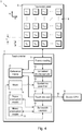
- FIG. 4 schematically illustrates a touchscreen system 5 including a touchscreen panel 6 and a touch controller 7.
- a touchscreen panel includes a two dimensional N by M grid 8 of sensor areas I n,m .
- I n,m denotes the n th of N sensor areas spaced apart in a first direction d 1 and the m th of M sensor areas spaced apart in a second direction d 2 .
- the first and second directions d 1 , d 2 may be, for example, perpendicular x and y directions.
- Sensor areas I n,m have a characteristic dimension 1 and are spaced apart in the first and second directions d 1 , d 2 by an amount s.
- the sensor areas I n,m have an active area A s , and may or may not have the same shape in the first and second directions d 1 , d 2 .
- the sensor areas I n,m may or may not be spaced apart by the same amount s in the first and second directions, for example l 1 ⁇ l 2 .
- Each sensor area I n,m is typically defined by the overlap or intersection of an electrode X n extending in the first direction d 1 and an electrode Y m extending in the second direction d 2 , the first electrodes X 1 , ..., X n , ..., X N and second electrodes Y 1 , ..., Y m , ..., Y M defining the grid 8.
- each sensor area I n,m may alternatively be a discrete sensor.
- the sensor areas I n,m may produce signals indicating one or more of a capacitance, a resistance and a pressure, depending on the type of touchscreen panel 6.
- the touch controller 7 includes a frame reading module 9, a correlated double sampler 10, a reference frame store 11 and a touch decision module 12.
- the touch controller 7 optionally includes a spatial low pass filter 13, a filter mask store 14, a bandwidth decision module 15, a signal attenuation model store 16 and a noise attenuation model store 17.
- the frame reading module 9, the correlated double sampler 10, the touch decision module 12 and optionally the spatial low pass filter 13 and the bandwidth decision module 15 may be provided by one or more hardware modules, or they may be provided as modules executed by one or more data processors.
- the reference frame store 11 and optionally the filter mask store 14, signal attenuation model store 16 and noise attenuation model store 17 may be provided by, for example, volatile or non-volatile memory (not shown) or a storage device (not shown).
- signal attenuation model store 16 and noise attenuation model store 17 are provided by a volatile memory, they may be stored in a non-volatile memory or storage device when the touchscreen system 5 is not powered.
- the frame reading module 9 reads output signals from the sensor areas I n,m and collates them as a signal frame matrix or array.
- the output signal from the sensor area I n,m is denoted F(n,m) in which the integer indices n, m denote the row and column of an entry in the frame array which stores the output signal from the sensor area I n,m .
- the output signal from a sensor area I n,m is stored a relative location in the frame F(n,m) which corresponds to the relative location of the respective sensor area I n,m in the grid 8.
- the frame reading module 9 reads out frames F(n,m) at a scan frequency f s .
- the signals values of the first frame read out are denoted F(n,m,i) and the signal values of the kth frame read out are denoted F(n,m,k).
- F(n,m,i) The signals values of the first frame read out
- F(n,m,k) When the touchscreen system 5 is initially powered up, the first frame F(n,m,k) read is stored to the reference frame store 11 as a reference frame F o (n,m).
- a frame F(n,m,k) can be treated in a similar way to an image, which allows touchscreen signals corresponding to a touch event to be visualised as an image, and also allows image processing methods to be applied to the signal frame F(n,m,k).
- the frame reading module 9 may scan through the sensor areas I n,m , for example a raster scan. Alternatively the frame reading module 9 may read out each sensor area I n,m simultaneously, for example, when sensor areas I n,m are discrete sensors rather than intersections of electrodes X n , Y m .
- the scan frequency f s is typically between about 20 Hz and about 200 Hz. Faster and slower scan frequencies f s are in principle possible, however, slower scan frequencies f s may result in slow response times or failures to register short touch events, and faster scan frequencies f s may be redundant given typical speeds of user interaction.
- the frame reading module 9 may be active or passive.
- excitation signals maybe addressed to the sensor area I n,m being read in addition to reading an output signal.
- the frame reading module sends excitation signals to a drive electrode D n and reads output signals from a sense electrode S m .
- the frame reading module 9 is passive, the frame reading module only receives, and optionally amplifies, output signals from the sensor areas I n,m .
- the frame reading module 9 may receive and amplify charge from piezoelectric sensors in a pressure sensing touchscreen panel.
- the frame reading module 9 may combine active and passive reading of several quantities concurrently, for example, capacitance and pressure.
- the index k is used to distinguish between, for example, the presently read signal frame F(n,m,k) and the next signal frame F(n,m,k+1), and there is no upper bound for k.
- the corrected frame F CDS (n,m,k) may be represented, for each value of k, as a array or matrix in which the integer values n, m denote the row and column of an entry.
- the correlated double sampler 10 removes or reduces offsets 3 and common-mode components of the noise 4, which may reduce the possibility of the touch decision module 12 mis-registering a touch event.
- the touch decision module 12 receives the corrected frame F CDS (n,m,k) and determines whether a touch event has occurred based on the signal values of the corrected frame F CDS (n,m,k). For example, the touch decision module 12 may apply a threshold value and register signal values F CDS (n,m,k) which exceed the threshold as corresponding to a single or multi-touch event. If the touch decision module 12 determines that a touch event has occurred, then touch information 18 characterising the touch event is determined and sent to a device central processing unit (CPU) 19.
- the touch information 18 may include information such as, for example, the number of touch events and the location of each touch event.
- the touch information 18 provides input to an operating system or application being executed by the device CPU 19.
- the touch information 18 may include force or pressure values. If the touch decision module 12 does not detect any touch events in the corrected frame F CDS (n,m,k), then the touch decision module 12 replaces the reference frame F 0 (n,m) with the current corrected frame F CDS (n,m,k).
- the stored reference frame F 0 is dynamically updated to reflect the most recently read frame in which no touch event occurs. This allows the touchscreen system 5 to dynamically adjust to changes in the noise 4 experienced by the touchscreen panel 6.
- the optional spatial low pass filter 13 may receive the corrected frame F CDS (n,m,k) from the correlated double sampler 10 and provide a filtered frame F LPSF (n,m,k) to the touch decision module 12.
- the filtered frame F LPSF (n,m,k) may be represented, for each value of k, as an array or matrix in which the integer values n, m denote the row and column of an entry.
- the spatial low pass filter 13 has been described as a linear filter, the spatial low pass filter 13 may be a non-linear filter such as, for example, a median filter.
- the bandwidth decision module 15 receives the filtered frame F LPSF (n,m,k) and touch information 18 from the touch decision module 12, and determines whether the bandwidth of the spatial low pass filter 13 requires adjustment.
- the bandwidth decision module 15 uses the touch information 18 to differentiate between touch signals and residual noise after correlated double sampling. For example, signal values F CDS (n,m,k), F LPSF (n,m,k) corresponding to sensors areas I n,m determined to be part of a touch event by the touch decision module are signal values, and any other non-zero signal values are residual noise.
- the bandwidth decision module 15 determines the attenuation of the touch signal and the attenuation of the residual noise, and determines whether the bandwidth of the spatial low pass filter 13 should be updated by replacing the coefficients C i,j stored in the mask store 14. For example, the bandwidth decision module 15 may tune the bandwidth of the spatial low pass filter 13 to maximise the attenuation of the residual noise whilst keeping the attenuation of the touch signals below a threshold amount.
- the bandwidth decision module 15 may update the bandwidth of the spatial low pass filter 13 by incremental amounts. Alternatively, the bandwidth decision module 15 may update the bandwidth of the spatial low pass filter 13 based on a signal attenuation model received from the signal attenuation model store 16 and a noise attenuation model received from the noise attenuation model store 17.
- a signal attenuation model describes a relationship between the attenuation of touch signals and the bandwidth of the spatial low pass filter 13.
- a noise attenuation model describes a relationship between the attenuation of noise signals and the bandwidth of the spatial low pass filter 13.
- touch controller 7 For details of the touch controller 7 will be described in relation to the first and second methods of processing output signals from a touchscreen panel 6.
- the first and second methods of processing output signals from a touchscreen panel 6 may be used with any type of touchscreen panel 6 which outputs signals corresponding to sensor areas I n,m arranged in a two dimensional grid or array arrangement 8.
- any type of touchscreen panel 6 which outputs signals corresponding to sensor areas I n,m arranged in a two dimensional grid or array arrangement 8.
- a suitable type of touchscreen panel 6, namely a projected capacitance touchscreen namely a projected capacitance touchscreen.
- Projected capacitance touchscreen panels measure changes of capacitance at electrodes to detect a touch event.
- the term projected capacitance refers to the fact that electrodes of a projected capacitance touchscreen panel need not be physically touched by a conducting object to detect a touch event.
- electrodes of a projected capacitance touchscreen panel may be located behind a screen, for example made of glass or transparent polymer.
- a conducting object such as, for example, a user's digit 22 ( figure 6B ) or a conductive stylus touches the screen, the electric field lines will be perturbed, thus modulating the charge distribution and hence the capacitance.
- Projected capacitance touchscreen panels may operate according to self-capacitance of individual electrodes or mutual capacitance between pairs of electrodes.
- Mutual capacitance operation supports multi-touch events, and may be less sensitive to electromagnetic interference (EMI).
- EMI electromagnetic interference
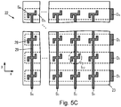
- FIGS. 5A, 5B and 5C schematically illustrate exemplary arrangements of electrodes for a projected capacitance touchscreen panels 20, 21, 22 using mutual capacitance.
- a first projected capacitance touchscreen panel 20 includes first electrodes X n , in the form of a number of drive electrodes D 1 , D 2 , ..., D N and second electrodes Y m in the form of a number of sense electrode S 1 , S 2 , ..., S M disposed on a layer of dielectric material 23.
- the layer of dielectric material 23 extends in a plane defined by first and second perpendicular directions x, y, and has a thickness in a third direction perpendicular to the first and second directions x, y which is substantially less than any in-plane dimension of the dielectric layer 23.
- the sense electrodes S m are disposed on a first surface of the dielectric layer 23, for example, an upper surface, and the drive electrodes D n are disposed on a second surface of the dielectric layer 23 which is opposite to the first surface in the third direction.
- the drive electrodes D n take the form of rectangular strips of conductive material, elongated in the first direction x and oriented parallel to each other.
- the drive electrodes D n are spaced apart by an amount s in the second direction y perpendicular to the first direction x.
- the sense electrodes S m take the form of rectangular strips of conductive material, elongated in the second direction y and oriented parallel to each other.
- the sense electrodes S m are spaced apart by an amount s in the first direction x perpendicular to the second direction y.
- the dielectric material layer 23 is commonly transparent when the projected capacitance touchscreen panel 20 overlies or is incorporated into a display, for example a organic light emitted diode (OLED) or liquid crystal (LC) display.
- the dielectric material layer 23 may be glass, or may be a transparent polymer such as, for example, polyethylene terephthalate (PET) or similar plastics.
- the drive and sense electrodes, D n , S m may also be transparent when the projected capacitance touchscreen panel 20 overlies or is incorporated into a display.
- drive and second electrodes D n , S m may be formed form indium tin-oxide (ITO) or indium zinc-oxide (IZO).
- a second projected capacitance touchscreen panel 21 is the same as the first projected capacitance touchscreen panel 20, except that the drive and sense electrodes D n , S m are different shapes.
- the drive electrodes D n take the form of a number of diamond shaped regions of conductive material 24 spaced apart in the first direction x and connected by narrow strips of conductive material 25.
- the sense electrodes S m may take the form of a number of diamond shaped regions of conductive material 26 spaced apart in the second direction y and connected by narrow strips of conductive material 27.
- a third projected capacitance touchscreen panel 22 is the same as the first and second projected capacitance touchscreen panels 20, 21, except that the drive and sense electrodes D n , S m are different shapes.
- the drive electrodes D n may take the form of rectangular strips which are elongated in the first direction x and which have a relatively greater width in the second direction y compared to the drive electrodes D n of the first projected capacitance touchscreen panel 20.
- the sense electrodes S m may take the form of a number of relatively narrow "Z-shaped" regions of conductive material 28 spaced apart in the second direction y and connected by narrow strips of conductive material 30.
- the drive and sense electrodes D n , S m of the third projected capacitance touchscreen panel 22 are arranged so that each Z-shaped conductive region 28 of a sense electrode S m is located overlying a corresponding drive electrode D n .
- the drive and sense electrodes D n , S m of the third projected capacitance touchscreen panel 22 are dimensioned, in particular the width of each drive electrode D n , so that no part of a Z-shaped conductive region 28 does not overlie a respective drive electrode D n . This is sometimes referred to as a "flooded" configuration.
- the sense electrodes S m need not use Z-shaped conductive regions 28, and other narrow shapes overlying a drive electrode D n maybe used such as, for example, "H-shaped" or "I-shaped” conductive material regions.
- Electrodes labelled as drive electrodes D n in the first, second and third projected capacitance touchscreen panels may alternatively be operated as sense electrodes S n and electrodes labelled as sense electrodes S m may alternatively be operated as drive electrode D m .
- electrode need not have a fixed role and may alternate between being a drive electrode and a sense electrode.
- a projected capacitance touchscreen panel need not use electrode arrangements described in relation to the first, second or third projected capacitance touchscreen panels 20, 21, 22.
- any two-dimensional grid or array of electrodes suitable for measuring mutual capacitance between pairs of electrodes may be used.
- Figure 6A shows a schematic cross-section of a projected capacitance touchscreen panel 20, 21, 22.
- Figure 6B shows a schematic cross-section of a projected capacitance touchscreen panel 20, 21, 22 during a touch event.
- the electrodes of a projected capacitance touchscreen panel 20, 21, 22 may be covered over with a cover lens 30.
- the cover lens 30 is generally transparent and may be formed of transparent materials such as, for example, of glass or PET.
- Each intersection of drive and sense electrodes D n , S m defines a sensor area I n,m , and each intersection I n,m may be measure individually by the frame reading module 9 of the touch controller 7 addressing the appropriate combination of drive and sense electrodes D n , S m .
- the drive electrode D n corresponding to an addressed intersection I n,m is driven by a driving signal 31, and am output signal 32 is read out from the respective sense electrode S m of the addressed intersection I n,m .
- the driving signal 31 may take the form of a voltage signal such as, for example, a sinusoidal waveform, a square waveform, other AC/pulsed waveforms or a DC bias voltage.
- Each pairing of drive and sense electrodes D n , S m defines an intersection which provides a sensor area I n,m , and all of the intersections I n,m may be sequentially read out to measure a complete signal frame F(n,m,k) from the projected capacitance touchscreen panel 20, 21, 22. In this way, both single-touch events and multi-touch events may be registered.
- the drive and second electrodes D n , S m corresponding to any given intersection I n,m define a baseline mutual capacitance, C M .
- the mutual capacitance between the drive and sense electrodes D n , S m is determined by the frame reading module 9 based on the driving signal 31 and the output signal 31.
- the frame reading module 9 may determine the mutual capacitance between the drive and sense electrodes D n , S m using any known method such as, for example, based on a change in the amplitude, phase or frequency of the driving/output signals 31, 32 compared to a reference signal.
- the frame reading module 9 may determine the mutual capacitance based on the time constant and/or charging/discharging times of the drive and second electrodes D n , S m .
- an additional capacitance C F couples the electrodes and the user's digit 33 or a suitable conductive stylus (not shown).
- the additional capacitance C F causes the mutual capacitance measured by the processor or touch controller to differ from the baseline mutual capacitance C M by an amount ⁇ C.
- the magnitude of the capacitive change ⁇ C during a touch event is not fixed, and may vary depending upon factors such as, for example, the contact area of the user's digit 33 or the suitable conductive stylus.
- a signal frame values F(n,m,k) read out from a projected capacitance touchscreen panel 20, 21, 22 is an array of the values of capacitance measured for each intersection I n,m of the drive and sense electrodes D n , S m .
- ⁇ C the amount of capacitive change ⁇ C exceeds a threshold amount, a touch event is registered.
- Noise 4 and offsets 3 will affect the measured capacitances, as previously described.
- the first and second methods of processing output signals from touchscreen panels are not limited to projected capacitance touchscreen panels 20, 21, 22 using mutual capacitance.
- the first and second methods of processing output signals from touchscreen panels may alternatively be used with projected capacitance touchscreen panels using self-capacitance, or with touchscreen panels based on measuring different properties such as, for example, electrical resistance or pressure.
- the first and second methods of processing output signals from touchscreen panels may alternatively be used with touchscreen panels based on optical or acoustic methods.
- the first and second methods of processing output signals from touchscreen panels may be used with any touchscreen panel 6 in which the contact area of a user's digit 33 or a stylus generates a signal from more than one sensor area I n,m .
- a touchscreen panel 6 may include a grid 8 formed by intersections between a number N of electrodes X 1 , ..., X n , ...X N extending in a first direction d 1 and a number M of electrodes Y 1 , ..., Y m , ..., Y M extending in a second direction d2.
- the electrodes X n , Y m may be drive and sense electrode D n , S m .
- the electrodes X n , Y m may fulfil different roles.
- the signal frame values F(n,m,k) may represent and be proportional to a capacitance or change in capacitance between the drive and sense electrodes D n , S m .
- the signal frame values F(n,m,k) may represent and be proportional to a resistance or change in resistance between the respective electrodes X n , Y m .
- the signal frame values F(n,m,k) may represent and be proportional to a pressure or force applied between the respective electrodes X n , Y m .
- the signal frame values F(n,m,k) need not correspond to the sensor areas I n,m defined by intersections between electrodes X n , Y m .
- the sensor areas I n,m may correspond to the discrete sensors so that each frame signal value F(n,m,k) corresponds to the signal obtained from a respective sensor.
- the first and second methods of processing out signals from a touchscreen panel may be applied to reduce or remove noise 4 and offsets 3 to improve the SNR and reduce mis-registrations of touch events.
- SNR Signal-to-noise ratio
- a SNR > 1 implies that the touch signal, for example F(n,m,k) exceeds the noise 4.
- the offset 3 is not dealt with as a noise component, as it can be removed by deducting a fixed value. This is because the noise 4 typically varies rapidly, whereas the offsets 3 are typically constant or slowly varying.
- an acceptable value of the SNR may be greater than 1, greater than 2, greater than 3 or greater than 5.
- a lower SNR for example SNR > 1 may be acceptable in some applications, for example when only the registration of the presence or absence of a touch event is measured. However, for other applications, for example, for analog pressure sensing/force touch, a greater SNR may be needed to allow different levels of pressure applied by a user's interaction to be distinguished.
- FIGS. 7A and 7B schematically illustrate voltage output signals from a projected capacitance touchscreen panel 20, 21, 22.
- the output signal 32 from an intersection I n,m of a projected capacitance touchscreen panel 20, 21, 22 may take the form of a voltage signal V(t).
- the output signal V(t) generally includes contributions from a desired touch signal, V s , from an offset 3, V offset and from a noise signal 4.
- the noise 4 is a superposition of stochastic or random noise 1 and deterministic or common mode noise 2.
- the output signal V(t) may be corrected using correlated double sampling (CDS) to determine a corrected output signal V CDS (t).
- CDS correlated double sampling
- the background signal V o may be subtracted.
- the offset 3 and components of the noise 4 which are correlated between the output signal V(t) and the background signal V o may be substantially reduced or cancelled.
- the corrected output signal V CDS (t) substantially includes the desired signal V s and higher frequency uncorrelated components of the noise 4.
- CDS is applied to the frame signal values F(n,m) from each intersection In,m using an individual background reference value F o (n,m).
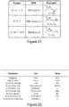
- Figure 21 illustrates different ranges of the characterization factor ⁇ applied to a case of a harmonic, single frequency, common-mode noise signal.
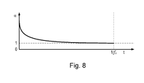
- Figure 8 schematically depicts the relationship between the characterization factor ⁇ and the scan frequency, f s .
- the characterization factor ⁇ may be considered to be inversely proportional to the scan interval 1/ f s .
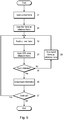
- Figure 9 shows a process flow diagram of a first method of processing output signals F(n,m,k) from a touchscreen panel 6.
- a first frame F(n,m,i) is read out by frame reading module 9 (step S1).
- the first frame F(n,m,i) is read out by sequentially scanning through each intersection I n,m by addressing the corresponding drive and sense electrodes D n , S m .
- a background pattern or reference frame F o (n,m) is initially set equal to the first frame F(m,n,i), and stored in the reference frame store 11 (step S2).
- the frame reading module 8 reads out signal frames F(n,m,k) (step S 3 ).
- the signal frame F(n,m,k) is read out by sequentially scanning through each intersection I n,m by addressing the corresponding drive and sense electrodes D n , S m .
- the read out of the signal frame F(n,m,k) may be synchronised with a display (not shown) which underlies the touchscreen panel 6 or into which the touchscreen panel 6 is embedded.
- the signal frame F(n,m,k) may be read out during a display quiet/blinking period.
- the correlated double sampler 10 receives the signal frame F(n,m,k) and applies a CDS correction by subtracting the reference frame F o (n,m) to generated a corrected frame F CDS (n,m,i) according to Equation 1 (step S4).
- the CDS correction maybe effective in reducing or removing offsets 3 because the offsets are constant or only slowly vary between reading out successive frames F(n,m,k), F(n,m,k+1).
- the CDS correction may be effective in reducing or removing low-frequency common-mode components of the noise 4 which are correlated between successive frames F(n,m,k), F(n,m,k+1).
- the touch decision module 12 receives and analyses the corrected frame F CDS (n,m,k) to determine whether a touch event, for example a single-touch event or a multi-touch event is occurring (step S5). If a touch event is not occurring (step S 5 ; No), the reference frame F 0 (n,m) is updated by overwriting the reference frame F o (n,m) stored in the reference frame store 11 with the current signal frame F(n,m,k) (step S8), and the next signal frame F(n,m,k+1) is read out by the frame reading module 9 (step S 3 ).
- the touch decision module determines and outputs the touch information 18 to the device CPU 19 (step S6).
- the touch information can be used by an application of operating system being executed by the device CPU 19 to select an option, open a folder on desktop or to close a web browser application. Whilst the touchscreen system 5 continues operating (step S7), the next signal frame F(n,m,k+1) is read out (step S 3 ).
- steps S4 to S8 are preferably conducted in less time than the scan interval 1/ f s .
- the steps occurring between reading out a signal frame F(n,m,k) and reading out a subsequent signal frame F(n,m,k+1) preferably do not take longer than the interval between display quiet/blanking periods.
- CDS maybe applied to signal frames read out from a touchscreen panel 6 in order to reduce or cancel offsets 3 and low frequency common-mode components of noise 4.
- This may improve the SNR of the touchscreen system 5 and enable the excitation power and/or detection thresholds to be reduced for the touchscreen system 5. This may extend the battery life of a device incorporating the touchscreen system by reducing power consumption. Improved SNR of the touchscreen system 5 may also improve the accuracy of a touchscreen system 5 by reducing the probability of mis-registering a touch event.
- the reference frame F o (n,m) is kept up to date with the most recent, and thus most accurate, background pattern of noise and offsets.
- Changes in the ambient environment may encompass changes in the number, type and proximity of sources of electromagnetic noise, changes in temperature, or changes such as plugging in or unplugging a mobile device incorporating the touchscreen system 5 from a charging cable.
- the use of the first method of processing output signals from a touchscreen panel may be illustrated with reference to experiments conducted using an example of a projected capacitance touchscreen panel.
- Figure 22 is a table providing details of the projected capacitance touchscreen panel used for testing the first method of processing output signals from a touchscreen panel.
- the experimental touchscreen panel was rectangular, with a diagonal dimension of 10.1 inches (25.7 cm) and had an aspect ratio of 16:9.
- the excitation voltage for the drive electrodes D n was 10 V.
- the drive electrodes D n had a width of 3 mm.
- the portions of the sense electrodes S m which overlapped the drive electrodes D n had a maximum width of 449 ⁇ m.
- Signal frames F(n,m,i) were read out at a frequency of 30 Hz or 60 Hz.
- the pixels of a display underlying the example touchscreen panel had dimensions of 56 ⁇ m by 56 ⁇ m.
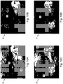
- Figures 10A and 10B show grayscale illustrations of a single-touch event frame 34 and a corresponding CDS corrected single-touch event frame 35.
- Figures 10C and 10D show grayscale illustrations of a multi-touch event frame 36 and a corresponding CDS corrected multi-touch event frame 36.
- regions labelled "DB” correspond to low signal levels
- regions labelled "LB” correspond to intermediate signal levels
- regions labelled "R” correspond to high signal level.
- applying the first method of processing output signals from a touchscreen panel to a multi-touch event frame 36 results in a significant reduction in offsets 3 and noise 4 of the corresponding CDS corrected multi-touch event frame 37.
- the contrast of the touch signals is substantially improved in the CDS corrected frames 35, 37 processed according to the first method of processing output signals from a touchscreen panel.
- accurately determining the number and locations of touch events may be improved.
- significant offset 3 signals which could lead to false registration of touch events, for example the regions coloured red towards the upper portion of the uncorrected signal frames 34, 36, are removed by the processing according to the first method.
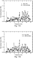
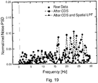
- Figures 11A and 11B show power spectral density (PSD) plots of the normalised noise output from the experimental touchscreen panel at 60 and 30 Hz respectively.
- Normalised noise refers to signal frames recorded without any touch events.
- the effect of the first method on the noise properties of the experimental touchscreen panel was investigated by reading out signal frames F(n,m,k) in the absence of any touch events. Without touch events, and hence without touch signals, the read out frames F(n,m,k) consist substantially of noise 4 and offsets 3.
- the effects of the first method may be investigated by calculating and comparing the PSD of the signal frames F(n,m,k) and the corrected frames F CDS (n,m,k) in the absence of any touch events.
- the frequency range in which an improvement is observed after correction using the first method is reduced to below about 3 Hz.
- the reduced frequency range of improvements at reduced scan frequency f s may result from a relatively weaker correlation of low-frequency noise between adjacent frames at reduced sampling frequencies.
- the correlation of noise between adjacent frames may be relatively increased for higher sampling frequencies. Because the offsets 3 behave as DC, they can be cancelled regardless of sampling frequency.
- CDS may have the effect of introducing higher frequency noise within a certain bandwidth. This effect is related to the sampling frequency and will be explained with reference to the following example, in which a harmonic, single frequency, noise waveform, H(t), with a frequency f s /2, is subject to CDS correction at a scan frequency f s . The interval between two adjacent sampling times is then equal to phase of ⁇ .
- H CDS is the noise signal after applying CDS
- H 0 is amplitude of the noise waveform H(t)
- ⁇ is the initial phase of the noise waveform H(t)
- t is time. Equation 5 indicates that a noise waveform, for example H(t) having a frequency f s /2 of half the CDS sampling frequency f s , the amplitude of the noise waveform H CDS after CDS is doubled. Similar analysis can be made for other ratios of noise waveform and scan frequency f s .
- the modest in noise components at higher frequencies as a result of applying the first method may be mitigated by filtering out higher frequency components. This is possible because signals corresponding to touch-events are typically low frequency, for example, user interactions with a touchscreen panel typically occur at frequencies a few Hz or less.
- the experimental results show that up to about 10% of the scan frequency f s , the SNR may be boosted by 5.9 dB and 7.6 dB when the scan frequencies f s are 30 Hz and 60 Hz, respectively. Above about 10% of the scan frequency f s , the SNR does not improve and may even be degraded.
- the first method of processing output signals from a touchscreen panel may substantially reduce common-mode components of noise 4 and offsets 3 within the frequency band containing touch signals.
- the first method of processing output signals from a touch panel may remove or reduce of offsets 3 and low frequency common-mode components of the noise 4.
- the time taken for the repeated steps of the first method should preferably not exceed the scan interval 1/ f s between reading out successive signal frames F(m,n,k), F(m,n,k+1).
- the computational time for the CDS correction of the first method should be less than 16.7 ms.
- Computational time generally depends on the complexity of an algorithm.
- the number of intersections I n,m to be scanned for the touchscreen panel 6 is N ⁇ M.
- the computational time of the first method scales as O(N ⁇ M).
- the first method may be implemented in a device incorporating a touchscreen system 5 without the need to reduce the scan frequency f s .
- P total ENM f s in which P is the processor or touch controller power use, E is the energy for measuring one intersection, N and M are grid 8 dimensions and f s is the scan frequency.
- E CDS N ⁇ M ⁇
- E CDS is the power consumption of the CDS operation
- N and M are grid 8 dimensions and ⁇ is the power efficiency of the processor or touch controller.
- Examples of currently used embedded processors for example an ARM (RTM) Cortex (RTM) A 5 processor, have a power efficiency ⁇ in the range of 20 million instructions per second (MIPS)/mW.
- the power consumption ECDS may be of the order of 7.2nW, and the computation time is of the order of 0.14 ⁇ s.
- the additional energy consumption from applying the first method is of the order of 1fJ, which is substantially smaller than the energy consumption of commonly used processors or touch controllers.
- the first method of processing output signals from a touchscreen panel 6 may provide substantial improvements in offsets 3 and low frequency common-mode components of the noise 4.
- the correlation between a signal frame F(n,m,k) and the noise reference frame F 0 (n,m) becomes weak, noise spikes may remain, especially at higher frequencies.
- the signal from a touch event may have a lower spatial frequency compared to the noise spikes.
- a second method of processing output signals from a touchscreen panel combines CDS correction of signal frames F(m,n,k) according to the first method with spatial filtering of the corrected frames F CDS (n,m,k) using a spatial low pass filter 13.
- Figure 12 illustrates spatial filtering to reduce the magnitude of a noise spike.
- regions labelled "DB” correspond to low signal levels
- regions labelled "LB” correspond to intermediate signal levels
- regions labelled "R” correspond to high signal level.
- a corrected signal frame F CDS (n,m,k) may include noise spikes 38 which result from, for example, random components of noise 4 or high frequency common mode components of noise 4 which are uncorrelated with the reference frame F 0 (n,m) used for the CDS correction.
- a noise spike 38 may take the form of, for example, an abnormally high signal value F CDS (n,m,k) at an intersection I n,m when compared to the signal values, e.g. F CDS( n+1,m,k), F CDS (n,m+1,k) etc, at surrounding intersections, e.g. I n+1,m , I n,m+1 etc.
- the corrected frame F CDS (n,m,k) may be processed using a spatial low pass filter 13 to produce a filtered frame, F LPSF (n,m,k).
- the spatial low pass filter 13 has the effect of averaging the noise spike 38 by mixing it with adjacent intersection values, resulting in a filtered spike 39 with reduced magnitude.
- Spatial filtering to touch signals has the potential to introduce unwanted effects.
- the touch signal may also be reduced by the spatial low pass filter 13, sometimes referred to as a "smoothing effect", which may decrease SNR and potentially increase the probability of failing to register a touch.
- the smoothing effect has the potential to distort the apparent location of a touch due to the coupling to the signal values for adjacent/nearby intersections I n,m .
- Careful design of spatial low pass filter 13 may allow noise spikes 38 to be attenuated whilst minimizing the attenuation of the touch signals and avoiding distortion of the touch location.
- digits 33 which present different contact areas to a touchscreen panel 6.
- the same user may vary which digits 33 contact the touchscreen panel and may sometimes use a stylus (not shown) instead of a digit 33.
- Application of a single bandwidth for the spatial low pass filter 13 may not be suitable for all possible users and/or styluses.
- the bandwidth of a spatial low pass filter 13 is dynamically tuned during use to optimise between attenuating noise spikes 38 and preserving the integrity of touch signals.
- Devices which incorporate touchscreen panels are frequently mobile devices which may operate under battery power in use.
- battery operated devices typically include rechargeable batteries, and must be periodically connected to a charging supply or charger (not shown) in order to replenish the battery. The device may still be used whilst connected to the charger.
- Chargers commonly take the form of a transformer-rectifier circuit which converts high voltage AC power from an outlet into DC power at a voltage suitable for recharging the battery of a device. In an ideal charger, the conversion would be perfect and the charger would output a constant DC voltage. In practice, a charger will produce an output including common-mode fluctuations such as, for example, residual "ripple" current/voltage, noise spikes and other artefacts
- the peak common mode noise introduced by a charger may typical vary within a range from less than 3 V to more than 40 V, depending on the quality of the charger.
- Common-mode noise from a charger may not affect the operation of a capacitive touchscreen panel 20, 21, 22 when it is not being touched because the difference of the charger output is maintained.
- a touch event occurs, there are broadly two scenarios. First, the device incorporating the touchscreen panel 6 may be held by a hand. Second, the device incorporating the touchscreen panel 6 may be placed on surface or in a holder, for example on a table or a stand. When the device is held, it may be sufficiently grounded to the earth so that common-mode noise charge does not escape to ground. However, if the touchscreen panel 6 is placed on a surface or in a holder, i.e. when the touch panel and the human body do not share the same ground, the touch event generated by a finger may lead to touch mis-registrations.
- AMOLED active-matric organic light-emitting diodes
- LC liquid crystal
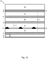
- Figure 13 shows an example stack-up 43 for a back-lit LC display incorporating a touchscreen panel which overlies an LC display.
- an example of an LC display stack-up 43 includes, in order moving away from a user, a cover lens 30, a first electrode layer 44, a layer of dielectric material 23, a second electrode layer 45, a touchscreen panel substrate 46, a first polarizer filter 47, a colour filter substrate 48, a common electrode, V com , layer 49, liquid crystal layer 50, thin film transistors (TFT) 51, pixel/sub-pixel electrodes 52, a TFT substrate 53, a second polarizer filter 54, a while backlight 55 and a reflector layer 56.
- TFT thin film transistors
- the first patterned conductive layer 44 provides, for example, a number N of electrodes X n extending in a first direction d 1 and the second patterned conductive layer 45 provides, for example, a number M of electrodes Y m extending in a second direction d 2 .
- the TFTs 51 are individual addressable and control the pixel/subpixel electrodes 52 to allow local re-orientation of liquid crystal molecules in the region of the liquid crystal layer 50 between the addressed pixel/sub-pixel electrode 52 and the V com electrode 49.
- the first capacitance C 1 couples the pixel/sub-pixel electrodes 52 and the V com layer 49.
- the first capacitance C 1 shields the display noise because the V com layer 49 has considerable resistance.
- the V com layer 49 may be made from ITO.
- the second capacitance C 2 couples the V com layer 49 and the second electrode layer 45.
- the second capacitance C 2 couples noise from the LC display to the touchscreen panel 6.
- the amount of coupled noise from an LC display may be measured by detecting a voltage induced in a conducting strip stacked directly onto an LC display.
- a voltage induced in a conducting strip stacked directly onto an LC display For example, an experiment was conducted using a copper strip stacked directly on an LC display in the form of a Dell (RTM) e198wfp LCD screen.
- the LC display noise coupled to the copper strip was measured using an Agilent (RTM) DSO-X 2024A oscilloscope.
- the area of the copper strip was 3mm ⁇ 3mm, which is a comparable area to the active area A s of a typical projected capacitance touchscreen panel 20, 21, 22.
- Figure 14 shows an oscilloscope trace of noise from an LC display detected by a copper strip placed over the LC display.
- the experimentally measured LC display noise signal 57 includes a strong deterministic component, which is expected to depend on the design of the product and to not significantly vary after the display is fabricated.
- Spatial low pass filters may be broadly characterised as linear filters or non-linear filters.
- Linear filters include filter types such as average filters and Gaussian filter.
- Non-linear filters include filter types such as median filters.
- Figure 15 schematically illustrates applying a mask 58 for a linear spatial low pass filter 13 to an array of corrected frame values F CDS (n,m,k).
- a linear filter mask 58 is applied to an array of corrected frame values F CDS (n,m,k).
- the linear filter mask 58 has dimensions L by W, which are typically positive odd integers to ensure that a single intersection I n,m is the centre of the linear filter mask 58.
- the optimal linear filter mask 58 dimensions L, W and coefficients C i,j for a given touchscreen panel 6 may depend upon the both the physical characteristics of the touchscreen panel 6 and the characteristics of the touch events such as the contact area of the user's digit 33 or of a suitable stylus.
- Linear filters as described in Equations 9 and 10 are preferred in general applications due to the simplicity of implementation, low processing requirements and balanced performance between digit 33 touches and stylus touches.
- Non-linear filters involve, for example, derivation of a filtered value using statistics such as determining a median value.
- Non-linear filters may be preferred for some applications because non-linear filters may potentially provide superior attenuation of noise spikes.
- non-linear filters may excessively attenuate signals of touch events corresponding to low contact areas, for example a stylus touch.
- the touch event When a user touches a touchscreen panel, for example a projected capacitance touchscreen panel 20, 21, 22, the digit 33 or stylus contacting the panel will not exclusively couple to a single electrode. Instead, the touch event will include signals from whichever intersection I n,m is closest to the touch point and also from adjacent or nearby intersections, for example I n + 1,m , I n,m+1 etc. In this way, the touch event has an interaction area 59 ( Figure 16A ) which encompasses multiple intersections I n,m of the drive and sense electrodes D n , S m .
- An interaction area 59 spanning multiple intersections I n,m is not limited to projected capacitance touchscreen panel 20, 21, 22 types, and other types of touchscreen panel such as, for example, pressure sensing touchscreen panels, may have interaction areas 59 which encompass several intersections I n,m .
- the linear filter mask 58 dimensions L, W are larger than the interaction area 59, then a spatial low pass filter 13 may reduce the relative strength of the touch signal, which may result in failure to register a touch event. Additionally, in order to avoid potential interference between two concurrent touch events, which may cause a skew in the registered position of a touch event, the linear filter mask 58 dimensions L, W should preferably be no larger than the typical interaction area 59 of a touch event.
- the dimensions L, W of the mask may be determined based on the typical size of a human digit 33 and the dimension 1 and spacing s of the active areas A s of sensor areas/intersections I n,m .
- Figures 16A and 16B illustrate a grid 8 of corrected frame values F CDS (n,m,k) with interaction areas 59 superimposed.
- a touch event centred on I n,m has an interaction area 59 which approximately encompasses a 3 by 3 block of intersections I n,m , i.e. n ⁇ 1, m ⁇ 1.
- F LPSF (n,m) the filtered frame value
- Equation 11 may be simplified to: F LPSF n m ⁇ F CDS n m k + 4 F CDS n + 1 , m , k + 4 F CDS n + 1 , m + 1 , k 9
- the filtered signal value F LPSF (n,m,k) may be approximated as: F LPSF n m k ⁇ F CDS n m k + 4 F CDS n m k ⁇ + 4 F CDS n m k ⁇ 9 F LPSF n m k ⁇ F CDS n m k ⁇ + 4 ⁇ + 4 ⁇ 9 bc
- the sensitivity of the filtered frame value F LPSF (n,m,k) to positional mis-registrations caused by noise spikes 38 may be evaluated by considering the conditions under which the filtered frame value of one of the nearest neighbour locations to the touch event, for example F LPSF (n,m+1), exceeds the filtered frame value F LPSF (n,m) at the touch event location.
- F CDS (n+1,m,k) F CDS (n,m+1,k) etc.
- F LPSF (n,m,k) > F LPSF (n,m+1,k) the inequality: F CDS n m k H > 3 ⁇ 3 ⁇ + ⁇ should be satisfied.
- the ratio F CDS (n,m,k)/H is related to the SNR.
- H is approximately two orders smaller than F(n,m), and the scaling parameters ⁇ , ⁇ typically lie in a range between one and three.
- the condition of Equation (17) may become dominated by the noise values H, resulting in increased probability mis-registering the location of a touch event.
- Equation 17 is not specific to projected capacitance touchscreen panels 20, 21, 22, and may equally apply to any touchscreen panel 6 which has an interaction area 59 for a touch event which encompasses more than one intersection I n,m .
- Signals corresponding to touch events are typically of relatively low spatial frequency compared to noise spikes, when the touch event is generated by user's digit 33.
- some types of touch events for example touch events generated by user input via a suitable stylus, may have relatively higher spatial frequency compared to a touch event generated by user input with a digit 33.
- a touch event generated by a stylus may have an interaction area 59 which encompasses a single intersection I n,m .
- noise spikes are typically considered to have high spatial frequency, for example to effect a single intersection I n,m , it is also possible for noise spikes to have spatial frequencies which are lower than a single intersection I n,m .
- One way to maximise attenuation of noise spikes 38 without detrimentally attenuating the desired touch signals is to dynamically tune the bandwidth of a spatial low pass filter 13 by dynamically adjusting the coefficients C i,j of a linear filter mask 58 with fixed dimensions L, W.
- a second method of processing output signals from a touchscreen panel applies a spatial low pass filter 13 using linear filter masks 58 having varying bandwidth determined by the coefficients C i,j of the linear filter mask 58.
- the amplitude G is preferably a normalisation factor to minimise an overall increase or decrease in the average intensity of the filtered frame values F LPSF (n,m,k) compared to the corrected frame F CDS (n,m).
- a touchscreen panel 6 having a grid 8 of intersections I n,m defined by electrodes X n (e.g. drive electrodes D n ) in a first direction d 1 (e.g. x) and electrodes Y m (e.g. sense electrodes S m ) in a second direction d 2 (e.g. y) need not be a square grid, and the standard deviations ⁇ n , ⁇ m may be different accordingly.
- a small value of standard deviation ⁇ indicates relatively weak coupling between an intersection I n,m and the other intersections encompassed by the linear filter mask 58, for example I n+1,m .
- a small value of standard deviation ⁇ therefore indicates relatively weaker attenuation of a noise spike 38 corresponding to a single intersection I n,m .
- a larger value of standard deviation ⁇ indicates stronger coupling between an intersection I n,m and the other intersections encompassed by the linear filter mask 58, for example I n+1,m .
- a larger value of standard deviation ⁇ therefore indicates relatively stronger attenuation of a noise spike 38 corresponding to a single intersection I n,m .
- the bandwidth of a spatial low pass filter 13 may be readily adjusted according to the value of the standard deviation ⁇ used to calculate the coefficients C i,j for the a Gaussian linear filter mask 48.
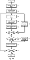
- Figure 18 shows a process flow diagram for a second method of processing output signals from a touchscreen panel.
- a first frame F(n,m,1) is read out by the frame reading module 9 upon start-up of the touchscreen system 5, (step S1) and a background pattern or reference frame F o (n,m) is initially set equal to the first frame F(m,n,1) and stored to the reference frame store 11 (step S2).
- the frame reading module 9 reads out signal frames F(n,m,k) at the scan frequency f s (step S3), and the correlated double sampler receives and corrects the signal frames F(n,m,k) by subtracting the reference frame F 0 (n,m) to generate corresponding corrected frames F CDS (n,m,k) (step S4 and Equation 1).
- the spatial low pass filter 13 receives the corrected frame F CDS (n,m,k) and filters it using a linear filter mask 58 to produce a filtered frame F LPSF (n,m,k) (step S9).
- the initial bandwidth of the spatial low pass filter 13 may be set to a predetermined value. Alternatively the initial bandwidth may be set to the finishing value of bandwidth from a previous occasion that the touchscreen system 5 was operating.
- the spatial low pass filter 13 may be a Gaussian filter characterised by a linear filter mask 58 in the form of an array of coefficients C i,j calculated according to Equation (18) with a standard deviation ⁇ .
- the standard deviation ⁇ may be set initially set to a predetermined value ⁇ 0 . Alternatively, the standard deviation ⁇ may be set to the finishing value of standard deviation ⁇ from a previous occasion that the touchscreen system 5 was operating.
- the touch decision module analyses the filtered frame F LPSF (n,m,k) to determine whether a touch event, for example a single-touch event or a multi-touch event is occurring (step S5). If a touch event is not occurring (step S5; No), the reference frame F 0 (n,m) is updated by overwriting the reference frame F 0 (n,m) equal stored in the reference frame store 11 with the current signal frame F(n,m,k) (step S8), and the next signal frame F(n,m,k+1) is read out by the frame reading module 7 (step S3).
- the bandwidth decision module 15 decides whether the bandwidth of the spatial low pass filter 13 is optimal or whether the bandwidth of the spatial low pass filter 13 should be changed (step S10).
- the bandwidth decision module 15 may evaluate the attenuation of the touch signals and the noise spikes 38 by comparing the CDS corrected frame F CDS (n,m,i) to the filtered frame F LPSF (n,m,i).
- any values of the corrected or filtered frames F CDS (n,m,k), F LPSF (n,m,k) corresponding to intersections I n,m determined to be part of a touch event by the touch decision module 12 are signal values, and any other non-zero values may be regarded as noise.
- a variety of criteria for adjusting the bandwidth of the spatial low pass filter 13 may be applied by the bandwidth decision module 15. For example, when the filter uses a Gaussian filter mask 58 with coefficients C i,j calculated according to Equation (18) with a standard deviation ⁇ , the bandwidth decision module 15 may increase or decrease the standard deviation ⁇ value to maintain the SNR at a threshold value. Alternatively, the processor or touch controller may increase or decrease the standard deviation ⁇ value to try and maximise the attenuation of noise spikes 38 whilst keeping the attenuation of touch signals above a threshold value.
- the bandwidth decision module 15 need not adjust the bandwidth incrementally, and may use predetermined signal/noise attenuation models received from the signal/noise attenuation model stores 16, 17.
- the bandwidth decision module 15 may select an optimal bandwidth for the spatial low pass filter 13 based on the characteristics of the noise 4 present in the frame. An example of measuring a model relating noise spike and signal attenuation to the spatial low pass filter 13 bandwidth is explained hereinafter.
- the bandwidth decision module 15 may select a value of the standard deviation ⁇ based on predetermined signal/noise attenuation models relating noise spike and signal attenuation to the value of standard deviation ⁇ .
- the bandwidth decision module 15 may use a combination of modelling and incremental alterations, for example, the processor or touch controller may employ machine learning methods or "fuzzy" methods to explore parameters close to a modelled value in order to improve the signal/noise attenuation models stored in the signal/noise attenuation model stores 16, 17 by adding additional data points.
- the bandwidth decision module 15 determines that the bandwidth of the spatial low pass filter 13 does needs adjusting (step S10; Yes)
- the bandwidth decision module 15 adjusts the bandwidth by overwriting the coefficients C i,j stored in the mask store 14 with updated coefficients C i,j (step S11).
- the touch decision module 12 determines and outputs the touch information 18 to the device CPU 19 (step S6). Whilst the touchscreen system 5 is operating (step S7), the next signal frame F(n,m,k+1) is read out by the frame reading module 9(step S3).
- step S10 If the bandwidth of the spatial low pass filter does not need adjusting (step S10; No), the touch decision module 12 determines and outputs the touch information 18 to the device CPU 19 (step S6).
- All the steps occurring between reading out a signal frame F(n,m,k) and reading out a subsequent signal frame F(n,m,k+1) are preferably conducted in less time than the scanning interval 1/ f s .
- the steps occurring between reading out a signal frame F(n,m,k) and reading out a subsequent signal frame F(n,m,i+k) preferably do not take longer than the interval between display quiet/blanking periods.
- noise spikes 38 which are not removed by the correlated double sampler 10, for example because they are uncorrelated to the reference frame F 0 (n,m), may be attenuated by the spatial low pass filter 13.
- This may further increase the SNR for outputs from a touchscreen panel 6, and enable the signal thresholds and/or excitation power to be further reduced compared to CDS corrections alone.
- the second method of processing output signals from a touchscreen panel uses a spatial low pass filter 13 which is dynamically updated. This may allow the signal processing to remain optimised when different users having different sized digits 33 use the touchscreen system 5 or when a user switches between using a digit 33 and using a stylus.
- Figure 19 shows normalized power spectral density (PSD) plots for the raw signal frames F(n,m,k), the frames after CDS correction F CDS (n,m,k) and the frames after CDS correction and spatial low pass filtering F LPSF (n,m,k).
- PSD power spectral density
- the high frequency noise which may be introduced by the CDS correction, as hereinbefore described, may be suppressed by the spatial low pass filtering.
- the CDS correction and spatial low pass filtering are complementary, in that the overall improvement in SNR may be superior to that obtained by simply summing the improvements from CDS or spatial low pass filtering applied individually.
- the SNR was observed to be increased by 15.6dB, and the signal and noise spike were observed to be attenuated by 4.51dB and 19.25dB respectively.
- Figure 20A shows plots of the noise spike attenuation and the touch signal attenuation plotted against the standard deviation ⁇ of a Gaussian filter mask 58. The plots were obtained from simulations based on the data from the experimental projected capacitance touchscreen panel.
- Measured relationships between the attenuation of touch signals and noise spikes 38 may be used in to produce signal/noise attenuation models 16,17 for use in the second method of processing signals from a touchscreen panel, as described hereinbefore.
- the observed relationships may be used as models to determine a value of standard deviation ⁇ which preserves the SNR above a threshold value if the amplitude of noise spikes increases.
- the measured relationships may be used as models to select an initial value for the standard deviation ⁇ 0 when the touchscreen system 5 starts up. For example, if an accepted signal attenuation is 2dB, then the initial Gaussian distribution based mask with standard deviation at o.6 would be used to maximally attenuate noise spikes without attenuating the touch signals by an unacceptable amount.
- the complexity of the second method of processing is increased to around O(3N). Similar calculations to those performed for the first method indicate that a typical commercially available processor for a mobile device would require approximately 19.2 ⁇ s and the power consumption of the algorithm would be 21.6 nW. Thus, the computational time of the second method is substantially less than the interval between frame read-outs for a typical scanning rate of 60 Hz, and the power consumption of the algorithm is negligible compared to the power consumption of reading out a frame.
- the second method may be used to improve SNR and remove offsets 3 without comprising the scan frequency f s or power consumption of a touchscreen system 5.
- a second method of processing signals from a touchscreen panel which combines CDS corrections with spatial low pass filtering.
- spatial low pass filtering may be applied directly to the signal frames F(n,m,k) read out by the frame reading module 9 to provide a modest improvement in SNR by smoothing of high frequency components of the noise 4.
- Transparent touchscreen panels 6 of a touchscreen system 5 have been described.
- the first and second methods are not limited to transparent touchscreen panels 6 overlying or integrated into a display screen.
- the first and second methods may also be applied to a touch panel, for example an opaque touch panel for providing input to a data processing device such as a laptop computer.
- a second method of processing signals has been described in which the bandwidth of a spatial low pass filter 13 is adjusted by a bandwidth decision module.
- the bandwidth need not be variable, and in some alternative methods the CDS correction according to the first method may be combined with spatial low pass filtering using a spatial low pass filter 13 having fixed bandwidth.
- the reference frame F 0 (n,m) the most recent signal frame F(n,m,k) which does not include a touch event is stored as the reference frame F 0 (n,m).
- this may result in an unexpected 'bad frame', for example resulting from a temporary hardware malfunction to be stored as the reference frame, possibly leading to a deterioration of SNR in subsequent frames.
- Other methods of updating the reference frame F o (n,m) may be used which are able to improve the robustness of the reference frame F o (n,m) updating. For example, by applying exponential smoothing so that the reference frame is assigned as: F 0 n m ⁇ ⁇ ⁇ F 0 n m + 1 ⁇ ⁇ F n m k in which ⁇ is a weighting factor. The weighting factor ⁇ can be adjusted to optimize performance. However, using exponential smoothing may weaken the correlation between adjacent frames. The trade-off between cancelling noise and robustness may depend on the application and the physical characteristics of the touchscreen panel 6.
- the efficiency of applying a linear filter mask 58 to frame values, F(n,m,k), F CDS (n,m,k) may be improved by not performing the summation in Equation 2 directly.
- an intermediate frame may be constructed in which each pixel contains the sum of 3 pixels in the first direction d 1 , x, for example F CDS (n,m,k)+ F CDS (n+1,m,k)+ F CDS (n+2,m,k).
- the final filtered image F LPSF (n,m,k) may be obtained by performing the same process on the intermediate image in the second direction d2, y, and then dividing by a scaling constant. This process is equally valid for Gaussian-weighted filters.
- Gaussian spatial low pass filters 13 have been described.
- any spatial low pass filters having a peak and a parameter for adjusting the relative width of the peak may be used instead of a Gaussian filter.
Landscapes
- Engineering & Computer Science (AREA)
- Theoretical Computer Science (AREA)
- General Engineering & Computer Science (AREA)
- Physics & Mathematics (AREA)
- General Physics & Mathematics (AREA)
- Human Computer Interaction (AREA)
- Multimedia (AREA)
- Signal Processing (AREA)
- Position Input By Displaying (AREA)
Description
- The present invention relates to processing signals from a touchscreen panel.
- Touchscreen panels (TSPs) are widely used in consumer electronic devices. Resistive and capacitive touchscreen panels have widely adopted as input means for data processing devices, in particular for mobile devices such as smartphones, tablet computers and laptops. There is also growing interest in pressure sensing touchscreen panels, for example as described in
US 2014/0008203 A1 . - Regardless of the mechanism used by a touchscreen panel to detect user inputs, mis-registration of user input is undesirable. For example, mis-registration of the presence or location of a user's interaction using a digit or stylus. There is also a need to keep the power consumption of touchscreen panels low to avoid shortening the battery life of mobile devices. Two of the main factors which influence touch registration and power consumption are noise and multi-valued offsets in the output signals from a touchscreen panel.
- Touchscreen panels are commonly arranged to record user interactions or touch events in a two dimensional grid or array arrangement. As used herein, the term "touch event" refers to a user interacting with a touchscreen by touching or pressing the touchscreen panel using a digit/finger or a suitable stylus. Herein, the signals output from a touchscreen panel having a two dimensional grid or array arrangement are collated into a corresponding array or frame. Such a frame may be presented as an image to help visualise the output signals from a touchscreen panel as a whole.
-
EP 2 693 316 A1 -
US 2013/176275 A1 describes control circuitry for a touch panel which includes a touch panel interface, a memory comprising touch positioning logic, and a controller in communication with the memory and the touch panel interface. The controller is operable, when the touch positioning logic is executed, to perform selected processing of the touch panel, including scanning a touch panel and determining a touch panel blob resulting from a touch, obtaining blob characteristics of the touch panel blob, and determining a position of the blob relative to the touch panel based on the blob characteristics. The blob characteristics can be adjusted to more accurately position the blob in circumstances where the blob is located near the edge of the touch panel, is in close proximity to another blob, or when the touch panel has variation in the received signal noise. -
US 2010/051354 A1 describes a method of matrix sensing using delay-based capacitance sensing, including using X-axis lines as active lines for capacitance measurements and using Y-axis lines as a disturbance to identify the location of a touch in a key matrix is disclosed. A sensing signal is applied to the X-axis lines, and a disturbance signal is applied to the Y-axis lines. If a location is touched, cross-capacitance is reduced, which is measured by sweeping data along the X-axis lines. -
Figure 1 illustrates noise sources in a touchscreen panel. In grayscale plots illustrating frames Fsingle, Fo, regions labelled "DB" correspond to low signal levels, regions labelled "LB" correspond to intermediate signal levels and regions labelled "R" correspond to high signal level. - Referring to
Figure 1 , noise signals in a touchscreen panel may come from many sources including, for example, stochastic, orrandom noise components 1, deterministic, or common-mode noise components 2 andoffsets 3.Stochastic noise components 1 represents random noise, for example, thermal noise from the touchscreen circuitry.Deterministic noise components 2 represents systematic sources, for example, mains electricity pick-up at 50-60 Hz, noise generated by a display, common-mode noise including power supply spikes induced by a charger for a mobile device.Deterministic noise components 2 encompasses regular but unintended signals in the touchscreen panel.Deterministic noise components 2 may be induced by other components of a device including a touchscreen panel, or may result from the ambient environment. The sum of thestochastic noise components 1 anddeterministic noise components 2 produces thenoise signal 4. In practice, it is often difficult or impossible to strictly divide thenoise 4 into stochastic 1 and deterministic 2 components, and different frequency bandwidths may include greater or lesser contributions from stochastic 1 and deterministic 2 components.Offsets 3 may be nonuniform across the grid or array of the touchscreen panel.Offsets 3 may arise because the readout from an individual electrode, an intersection of electrodes, a sensor etc, may in general have a slightly different DC offset.Offsets 3 need not be DC, and in some touchscreen panels theoffsets 3 may slowly vary or drift over time.Offsets 3 may result from the hardware of a device incorporating the touchscreen panel, or may result from factors in the ambient environment such as, for example, ambient temperature. Thenoise 4 combines with theoffsets 3 to produce a background noise frame Fo. When the touchscreen panel is touched, the resulting signal frame Fsingle is a superposition of the desired touch signals and the background noise frame Fo. -
Figures 2A, 2B and 2C illustrate touchscreen signal frames Fsingle, Fmulti, Fo. In greyscale plots illustrating touchscreen panel frames Fsingle, Fmulti, Fo, regions labelled "DB" correspond to low signal levels, regions labelled "LB" correspond to intermediate signal levels and regions labelled "R" correspond to high signal level. - Referring also to
Figures 2A, 2B and 2C , the touchscreen signal frames may be single touch signal frames Fsingle, multi-touch signal frames Fmulti or no-touch signal frames, such as background noise frame Fo. The term "single-touch" refers to a user interaction in which a single digit of a user, or a single suitable stylus touches or presses the touchscreen panel. The term "multi-touch" refers to a user interaction in which two or more digits of a user, or two of more suitable styluses, or a combination of a user's digits and a stylus, touch or press the touchscreen panel concurrently. - In an ideal touchscreen panel, the signal frames Fo, Fsingle, Fmulti would register zero everywhere except at the locations of user interactions. However, in general, almost all of the locations of a two dimensional grid or array arrangement of a touchscreen will have non-zero values, so that signals resulting from touch events must be large enough to overcome the
noise 4 andoffsets 3. - Consequently, the signal-to-noise ratio (SNR) of the touchscreen panel may be compromised, resulting in failures to register touch events and/or false registration of touch events which have not actually occurred. In order to achieve a high SNR, the excitation power may be increased for an active touchscreen panel or the amplification gain may be increased for a passive touchscreen panel. However, increasing the excitation power or amplification gain may increase the power consumption of a touchscreen panel and shorten battery life of a device incorporating the touchscreen panel. In touchscreen panels which provide analog outputs, for example in pressure sensing touchscreen panels, the SNR may limit the resolution of analog output signals, for example, force-touch signals.
- The
offset 3 of a single electrode, electrode intersection, sensor etc in a touchscreen panel may be cancelled by subtracting a fixed value or by applying a detection threshold which must be exceeded for a touch event to be registered. However, non-uniformity of theoffsets 3 across the touchscreen panel may make application of a single threshold or offset correction difficult, and may require a high threshold to avoid touch registration errors. -
Figure 3 illustrates touch signals obtained from a number of electrodes of a touchscreen panel. - Referring to
Figure 3 ,1 st to Nth electrode of a touchscreen panel have respective offset values Δ1, Δ2, ..., ΔN. A detection threshold for registering a touch event should be set at a level which at least exceeds the largest offset value Δ1, Δ2, ..., ΔN. For example, in a case when the output signals of a touchscreen panel are voltage signals corresponding to each electrode, a voltage threshold VTH should be set which at least exceeds the largest voltage offset value ΔV1, ΔV2, ..., ΔVN. Setting a detection threshold VTH according to the largest offset value ΔV1, ΔV2, ..., ΔVN may increase power consumption and may also reduce the dynamic range available for using analog output signals from, for example pressure sensing touchscreen panels. - The present invention seeks to provide improved processing output signals from a touch panel.
- According to a first aspect of the invention there is provided a method including receiving a first array of values obtained from measuring an array of touch panel sensor areas. The method also includes generating a second array of values based on subtracting a reference array of values from the first array of values, wherein generating the second array comprises generating a third array by subtracting the reference array from the first array, generating the second array by filtering the third array using a spatial low pass filter having a bandwidth equal to a reference bandwidth value. The method also includes determining presence of at least one touch event in dependence upon the second array of value and, upon a negative determination generating a new reference array based on exponential smoothing of the reference array and the first array using a weighting factor, or generating a new reference array which is equal to the first array, and storing the new reference array and, upon a positive determination outputting the second array. The method also includes determining, based on a difference of the second array and the third array, a first amount by which values corresponding to at least one touch event are attenuated and a second amount by which values not corresponding to any touch event are attenuated, generating a new reference bandwidth value based on the first amount and the second amount, and storing the new reference bandwidth value
- Thus, the values measured from an array of touch panel sensors may be corrected to remove or reduce noise signals and offsets of the sensor areas. Thus, a reference array used for the correction may be dynamically updated, allowing the correction to adapt to changes in the noise environment and/or drift in the sensor area offsets.
- A touch event may include a user interacting with the touchscreen panel by touching or pressing the touchscreen panel using a digit/finger or a suitable stylus. A touch event may include a user interacting with the touchscreen panel by placing a digit/finger or a suitable stylus in proximity to the touchscreen panel. A touch event may include a user touching the sensor areas directly or touching an outer surface of one or more layer separating the user from the sensor areas.
- Each value of the first array may be obtained from a direct measurement of a voltage, current or charge signal from the respective sensor area. Each value of the first array may be obtained based on one or more parameters of a voltage, current or charge signal directly measured from the respective sensor area. Each value of the first array may be obtained based on two or more voltage, current or charge signals directly measured from the respective sensor area and one or more other sensor areas.
- The touchscreen panel may include a plurality of first electrodes extending in a first direction and a plurality of second electrodes extending in a second direction different to the first direction. The first and second electrodes may form a grid and each intersection of the grid may define a respective sensor areas. Each sensor area of the sensor array may correspond to a respective discrete sensor.
- Thus, the bandwidth for spatial low pass filtering of the third array may be dynamically altered to optimise the relative attenuation of noise signals and touch signals. This may allow improved reduction of noise signals when changes occur in one or more of the ambient environment, the user of a touch panel sensor array and an input method of a user, for example from using a digit to using a stylus.
- Determining the new reference bandwidth value may include comparing the first amount to a predetermined threshold, and in dependence upon the first amount exceeding the threshold, generating the new reference bandwidth value by subtracting a bandwidth increment from the reference bandwidth value.
- In dependence upon the first amount not exceeding the threshold, the new reference bandwidth may be generated by adding the bandwidth increment to the reference bandwidth value. The bandwidth increment may be predetermined. The bandwidth increment may be dynamically determined based on the third matrix.
- Determining the new reference bandwidth value may include determining, based on a first model relating the first amount to the bandwidth value and a second model relating the second amount to the bandwidth value, an optimal bandwidth value such that the second amount is maximised without the first amount exceeding a predetermined threshold, and generating the new reference bandwidth based on the optimal bandwidth.
- The spatial low pass filter may be a linear filter. The spatial low pass filter may be a Gaussian filter and the reference bandwidth value for the spatial low pass filter may be a standard deviation of the Gaussian filter.
- Generating the second array by filtering the third array using a spatial low pass filter may include generating a fourth array, each entry of the fourth array calculated by summing at least three adjacent row entries of the third array including the corresponding entry of the third array, and generating the third array, each entry of the third array calculated by summing at least three adjacent column entries of the fourth array including the corresponding entry of the fourth array, and dividing by a respective scaling factor.
- The spatial low pass filter may be a non-linear filter.
- Each first array value may be based on the capacitance of the respective sensor area. Each first array value may be based on the force applied to the respective sensor area. Each entry of the first array may be a sub-array having a first value based on the capacitance of the respective sensor area and a second value based on the force applied to the respective sensor area, wherein operations performed on the first array are performed entry-wise on each sub-array.
- The method may enhance the signal-to-noise ratio for components of the output signals corresponding to touch events by 1 to 5 dB, 5 to 10 dB, 10 to 15 dB or more than 15 dB. The method may attenuate components of the output signals corresponding to noise signals by more 1 to 5 dB, 5 to 10 dB, 10 to 15 dB, 15 to 20 dB or more than 20 dB.
- According to a second aspect of the invention there is provided a computer program stored on a computer readable medium which, when executed by a data processing unit, causes the data processing unit to execute the method of processing output signals from a touchscreen panel.
- According to a third aspect of the invention there is provided an apparatus including one or more hardware modules or one or more processors configured to execute a frame reading module, a correlated double sampler, a touch decision module and a band with decision module. The frame reading module is configured to receive a first array of values obtained from measuring an array of touch panel sensor areas. The correlated double sampler is configured to generate a second array of values based on subtracting a reference array of values from the first array of values, wherein generating the second array comprises generating a third array by subtracting the reference array from the first array, and generating the second array by filtering the third array using a spatial low pass filter having a bandwidth equal to a reference bandwidth value. The touch decision module is configured to determine presence of at least one touch event in dependence upon the second array of values and, upon a negative determination generate a new reference array based on exponential smoothing of the reference array and the first array using a weighting factor, or generate a new reference array which is equal to the first array, and store the new reference matrix and, upon a positive determination output the second array. The bandwidth decision module is configured, in response to a positive determination of the presence of at least one touch event, to determine, based on a difference of the second array and the third array, a first amount by which values corresponding to at least one touch event are attenuated and a second amount by which values not corresponding to any touch event are attenuated, generate a new reference bandwidth value based on the first amount and the second amount, and store the new reference bandwidth value.
- A touch panel system may include a touch panel including a plurality of sensor areas disposed in a sensor array, each sensor area configured to provide an output signal which varies in response to a touch event, and the apparatus.
- Each given sensor area of the touch panel may be configured to provide an output signal based on the capacitance of the given sensor area. Each given sensor area of the touch panel may be configured to provide an output signal based on a force applied to the given sensor area. Each given sensor area of the touch panel may be configured to provide a single output single which is based on the capacitance of the given sensor area and the force applied to the given sensor area.
- Certain embodiments of the present invention will now be described, by way of example, with reference to the accompanying drawings in which:
-
Figure 1 illustrates noise sources in a touchscreen panel; -
Figure 2A illustrates signal frame from a single-touch event; -
Figure 2B illustrates signal frame from a multi-touch event; -
Figure 2C illustrates signal frame in the absence of any touch event; -
Figure 3 illustrates touch signals obtained from a number of electrodes of a touchscreen panel; -
Figure 4 schematically illustrates a touchscreen system including a touchscreen panel and a touch controller; -
Figure 5A schematically illustrates an electrode arrangement of a first projected capacitance touchscreen panel; -
Figure 5B schematically illustrates an electrode arrangement of a second projected capacitance touchscreen panel; -
Figure 5C schematically illustrates an electrode arrangement of a third projected capacitance touchscreen panel; -
Figure 6A schematically illustrates a projected capacitance touchscreen panel viewed side-on; -
Figure 6B schematically illustrates a projected capacitance touchscreen panel viewed side-on during a touch event; -
Figure 7A schematically illustrates a voltage output signal from a projected capacitance touchscreen panel; -
Figure 7B schematically illustrates a correlated double sampled voltage signal from a projected capacitance touchscreen panel; -
Figure 8 schematically depicts a relationship between an improvement in signal-to-noise-ratio and sampling frequency for correlated double sampling; -
Figure 9 shows a process flow diagram for a first method of processing output signals from a touchscreen panel; -
Figure 10A illustrates a signal from a single-touch event; -
Figure 10B illustrates a signal from a single-touch event following correlated double sampling; -
Figure 10C illustrates a signal from a multi-touch event; -
Figure 10D illustrates a signal from a multi-touch event following correlated double sampling; -
Figure 11A shows a power spectral density plot of normalised noise output from experiments conducted using the first method with a projected capacitance touchscreen panel with a scan frequency of 60 Hz; -
Figure 11B shows a power spectral density plot of normalised noise output from experiments conducted using the first method with a projected capacitance touchscreen panel with a scan frequency of 30 Hz; -
Figure 12 illustrates spatial filtering to reduce the magnitude of noise spikes; -
Figure 13 schematically illustrate an example stack-up for a back-lit liquid crystal display incorporating a touchscreen panel viewed side-on; -
Figure 14 shows an oscilloscope trace of noise from an LC display detected by a copper strip placed over the LC display. -
Figure 15 schematically illustrates applying a mask for a linear spatial low pass filter to an array of signal values; -
Figures 16A and 16B schematically illustrate grids of signal values; -
Figures 17A to 17D is a projection surface plot of the coefficients of a Gaussian filter mask with standard deviations of 0.5, 1, 2 and 4 respectively; -
Figure 18 shows a process flow diagram for a second method of processing output signals from a touchscreen panel; -
Figure 19 compares normalized power spectral density plots for raw output signals, correlated double sampled signals and correlated double samples and filtered signals; and -
Figures 20A and 20B plot noise spike attenuation and touch signal attenuation plotted against the standard deviation of a Gaussian filter mask. -
Figure 21 is a table illustrating different cases for applying correlated double sampling to a harmonic, single frequency, signal; and -
Figure 22 is a giving details of an experimental projected capacitance touchscreen panel used for testing first and second methods of processing output signals from a touchscreen panel; - In the following description, like parts are denoted by like reference numerals.
-
Figure 4 schematically illustrates atouchscreen system 5 including atouchscreen panel 6 and atouch controller 7. - Referring to
Figure 4 , a touchscreen panel includes a two dimensional N byM grid 8 of sensor areas In,m. In,m denotes the nth of N sensor areas spaced apart in a first direction d1 and the mth of M sensor areas spaced apart in a second direction d2. The first and second directions d1, d2 may be, for example, perpendicular x and y directions. Sensor areas In,m have acharacteristic dimension 1 and are spaced apart in the first and second directions d1, d2 by an amount s. The sensor areas In,m have an active area As, and may or may not have the same shape in the first and second directions d1, d2. The sensor areas In,m may or may not be spaced apart by the same amount s in the first and second directions, for example l1 ≠ l2. Each sensor area In,m is typically defined by the overlap or intersection of an electrode Xn extending in the first direction d1 and an electrode Ym extending in the second direction d2, the first electrodes X1, ..., Xn, ..., XN and second electrodes Y1, ..., Ym, ..., YM defining thegrid 8. However, each sensor area In,m may alternatively be a discrete sensor. The sensor areas In,m may produce signals indicating one or more of a capacitance, a resistance and a pressure, depending on the type oftouchscreen panel 6. - The
touch controller 7 includes aframe reading module 9, a correlateddouble sampler 10, areference frame store 11 and atouch decision module 12. Thetouch controller 7 optionally includes a spatiallow pass filter 13, afilter mask store 14, abandwidth decision module 15, a signalattenuation model store 16 and a noiseattenuation model store 17. Theframe reading module 9, the correlateddouble sampler 10, thetouch decision module 12 and optionally the spatiallow pass filter 13 and thebandwidth decision module 15 may be provided by one or more hardware modules, or they may be provided as modules executed by one or more data processors. Thereference frame store 11 and optionally thefilter mask store 14, signalattenuation model store 16 and noiseattenuation model store 17 may be provided by, for example, volatile or non-volatile memory (not shown) or a storage device (not shown). When thereference frame store 11 and optionally thefilter mask store 14, signalattenuation model store 16 and noiseattenuation model store 17 are provided by a volatile memory, they may be stored in a non-volatile memory or storage device when thetouchscreen system 5 is not powered. - The
frame reading module 9 reads output signals from the sensor areas In,m and collates them as a signal frame matrix or array. The output signal from the sensor area In,m is denoted F(n,m) in which the integer indices n, m denote the row and column of an entry in the frame array which stores the output signal from the sensor area In,m. In this way, the output signal from a sensor area In,m is stored a relative location in the frame F(n,m) which corresponds to the relative location of the respective sensor area In,m in thegrid 8. Theframe reading module 9 reads out frames F(n,m) at a scan frequency fs. The signals values of the first frame read out are denoted F(n,m,i) and the signal values of the kth frame read out are denoted F(n,m,k). When thetouchscreen system 5 is initially powered up, the first frame F(n,m,k) read is stored to thereference frame store 11 as a reference frame Fo(n,m). A frame F(n,m,k) can be treated in a similar way to an image, which allows touchscreen signals corresponding to a touch event to be visualised as an image, and also allows image processing methods to be applied to the signal frame F(n,m,k). - The
frame reading module 9 may scan through the sensor areas In,m, for example a raster scan. Alternatively theframe reading module 9 may read out each sensor area In,m simultaneously, for example, when sensor areas In,m are discrete sensors rather than intersections of electrodes Xn, Ym. The scan frequency fs is typically between about 20 Hz and about 200 Hz. Faster and slower scan frequencies fs are in principle possible, however, slower scan frequencies fs may result in slow response times or failures to register short touch events, and faster scan frequencies fs may be redundant given typical speeds of user interaction. Theframe reading module 9 may be active or passive. When theframe reading module 9 is active, excitation signals maybe addressed to the sensor area In,m being read in addition to reading an output signal. For example, in a projected capacitance touchscreen panel, the frame reading module sends excitation signals to a drive electrode Dn and reads output signals from a sense electrode Sm. When theframe reading module 9 is passive, the frame reading module only receives, and optionally amplifies, output signals from the sensor areas In,m. For example, theframe reading module 9 may receive and amplify charge from piezoelectric sensors in a pressure sensing touchscreen panel. Theframe reading module 9 may combine active and passive reading of several quantities concurrently, for example, capacitance and pressure. - The correlated
double sampler 10 receives the current signal frame F(n,m,k) from theframe reading module 9 and the reference frame Fo(n,m) from thereference frame store 11, and calculates a corrected frame FCDS(n,m,k) using correlated double sampling according to:
double sampler 10 removes or reducesoffsets 3 and common-mode components of thenoise 4, which may reduce the possibility of thetouch decision module 12 mis-registering a touch event. - The
touch decision module 12 receives the corrected frame FCDS(n,m,k) and determines whether a touch event has occurred based on the signal values of the corrected frame FCDS(n,m,k). For example, thetouch decision module 12 may apply a threshold value and register signal values FCDS(n,m,k) which exceed the threshold as corresponding to a single or multi-touch event. If thetouch decision module 12 determines that a touch event has occurred, then touchinformation 18 characterising the touch event is determined and sent to a device central processing unit (CPU) 19. Thetouch information 18 may include information such as, for example, the number of touch events and the location of each touch event. Thetouch information 18 provides input to an operating system or application being executed by thedevice CPU 19. When the touchscreen panel is a force or pressure sensing touchscreen panel, thetouch information 18 may include force or pressure values. If thetouch decision module 12 does not detect any touch events in the corrected frame FCDS(n,m,k), then thetouch decision module 12 replaces the reference frame F0(n,m) with the current corrected frame FCDS(n,m,k). - In this way, the stored reference frame F0 is dynamically updated to reflect the most recently read frame in which no touch event occurs. This allows the
touchscreen system 5 to dynamically adjust to changes in thenoise 4 experienced by thetouchscreen panel 6. - The optional spatial
low pass filter 13 may receive the corrected frame FCDS(n,m,k) from the correlateddouble sampler 10 and provide a filtered frame FLPSF(n,m,k) to thetouch decision module 12. The filtered frame FLPSF(n,m,k) may be represented, for each value of k, as an array or matrix in which the integer values n, m denote the row and column of an entry. The spatiallow pass filter 13 may take the form of a linear filter such as an average or Gaussian filter, and may filter the corrected frame FCDS(n,m,k) using a mask received from themask store 14 in the form of an matrix or array of coefficients Ci,j having dimensions L by W, according to:
double sampler 10, which may reduce the possibility of thetouch decision module 12 mis-registering a touch event. - Although the spatial
low pass filter 13 has been described as a linear filter, the spatiallow pass filter 13 may be a non-linear filter such as, for example, a median filter. - The
bandwidth decision module 15 receives the filtered frame FLPSF(n,m,k) andtouch information 18 from thetouch decision module 12, and determines whether the bandwidth of the spatiallow pass filter 13 requires adjustment. Thebandwidth decision module 15 uses thetouch information 18 to differentiate between touch signals and residual noise after correlated double sampling. For example, signal values FCDS(n,m,k), FLPSF(n,m,k) corresponding to sensors areas In,m determined to be part of a touch event by the touch decision module are signal values, and any other non-zero signal values are residual noise. Thebandwidth decision module 15 determines the attenuation of the touch signal and the attenuation of the residual noise, and determines whether the bandwidth of the spatiallow pass filter 13 should be updated by replacing the coefficients Ci,j stored in themask store 14. For example, thebandwidth decision module 15 may tune the bandwidth of the spatiallow pass filter 13 to maximise the attenuation of the residual noise whilst keeping the attenuation of the touch signals below a threshold amount. - The
bandwidth decision module 15 may update the bandwidth of the spatiallow pass filter 13 by incremental amounts. Alternatively, thebandwidth decision module 15 may update the bandwidth of the spatiallow pass filter 13 based on a signal attenuation model received from the signalattenuation model store 16 and a noise attenuation model received from the noiseattenuation model store 17. A signal attenuation model describes a relationship between the attenuation of touch signals and the bandwidth of the spatiallow pass filter 13. A noise attenuation model describes a relationship between the attenuation of noise signals and the bandwidth of the spatiallow pass filter 13. - For details of the
touch controller 7 will be described in relation to the first and second methods of processing output signals from atouchscreen panel 6. - The first and second methods of processing output signals from a
touchscreen panel 6 may be used with any type oftouchscreen panel 6 which outputs signals corresponding to sensor areas In,m arranged in a two dimensional grid orarray arrangement 8. However, before describing the first and second methods of processing output signals from atouchscreen panel 6, in may be helpful to briefly discuss one example of a suitable type oftouchscreen panel 6, namely a projected capacitance touchscreen. - Projected capacitance touchscreen panels measure changes of capacitance at electrodes to detect a touch event. The term projected capacitance refers to the fact that electrodes of a projected capacitance touchscreen panel need not be physically touched by a conducting object to detect a touch event. In general, electrodes of a projected capacitance touchscreen panel may be located behind a screen, for example made of glass or transparent polymer. When a conducting object such as, for example, a user's digit 22 (
figure 6B ) or a conductive stylus touches the screen, the electric field lines will be perturbed, thus modulating the charge distribution and hence the capacitance. - Projected capacitance touchscreen panels may operate according to self-capacitance of individual electrodes or mutual capacitance between pairs of electrodes. Mutual capacitance operation supports multi-touch events, and may be less sensitive to electromagnetic interference (EMI).
-
Figures 5A, 5B and5C schematically illustrate exemplary arrangements of electrodes for a projectedcapacitance touchscreen panels - Referring to
Figure 5A , a first projectedcapacitance touchscreen panel 20 includes first electrodes Xn, in the form of a number of drive electrodes D1, D2, ..., DN and second electrodes Ym in the form of a number of sense electrode S1, S2, ..., SM disposed on a layer ofdielectric material 23. The layer ofdielectric material 23 extends in a plane defined by first and second perpendicular directions x, y, and has a thickness in a third direction perpendicular to the first and second directions x, y which is substantially less than any in-plane dimension of thedielectric layer 23. The sense electrodes Sm are disposed on a first surface of thedielectric layer 23, for example, an upper surface, and the drive electrodes Dn are disposed on a second surface of thedielectric layer 23 which is opposite to the first surface in the third direction. The drive electrodes Dn take the form of rectangular strips of conductive material, elongated in the first direction x and oriented parallel to each other. The drive electrodes Dn are spaced apart by an amount s in the second direction y perpendicular to the first direction x. The sense electrodes Sm take the form of rectangular strips of conductive material, elongated in the second direction y and oriented parallel to each other. The sense electrodes Sm are spaced apart by an amount s in the first direction x perpendicular to the second direction y. - The
dielectric material layer 23 is commonly transparent when the projectedcapacitance touchscreen panel 20 overlies or is incorporated into a display, for example a organic light emitted diode (OLED) or liquid crystal (LC) display. For example, thedielectric material layer 23 may be glass, or may be a transparent polymer such as, for example, polyethylene terephthalate (PET) or similar plastics. The drive and sense electrodes, Dn, Sm may also be transparent when the projectedcapacitance touchscreen panel 20 overlies or is incorporated into a display. For example, drive and second electrodes Dn, Sm may be formed form indium tin-oxide (ITO) or indium zinc-oxide (IZO). - Referring also to
Figure 5B , a second projectedcapacitance touchscreen panel 21 is the same as the first projectedcapacitance touchscreen panel 20, except that the drive and sense electrodes Dn, Sm are different shapes. In the second projectedcapacitance touchscreen panel 21, the drive electrodes Dn take the form of a number of diamond shaped regions ofconductive material 24 spaced apart in the first direction x and connected by narrow strips ofconductive material 25. The sense electrodes Sm may take the form of a number of diamond shaped regions of conductive material 26 spaced apart in the second direction y and connected by narrow strips of conductive material 27. - Referring also to
Figure 5C , a third projectedcapacitance touchscreen panel 22 is the same as the first and second projectedcapacitance touchscreen panels capacitance touchscreen panel 22, the drive electrodes Dn may take the form of rectangular strips which are elongated in the first direction x and which have a relatively greater width in the second direction y compared to the drive electrodes Dn of the first projectedcapacitance touchscreen panel 20. The sense electrodes Sm may take the form of a number of relatively narrow "Z-shaped" regions ofconductive material 28 spaced apart in the second direction y and connected by narrow strips ofconductive material 30. The drive and sense electrodes Dn, Sm of the third projectedcapacitance touchscreen panel 22 are arranged so that each Z-shapedconductive region 28 of a sense electrode Sm is located overlying a corresponding drive electrode Dn. The drive and sense electrodes Dn, Sm of the third projectedcapacitance touchscreen panel 22 are dimensioned, in particular the width of each drive electrode Dn, so that no part of a Z-shapedconductive region 28 does not overlie a respective drive electrode Dn. This is sometimes referred to as a "flooded" configuration. The sense electrodes Sm need not use Z-shapedconductive regions 28, and other narrow shapes overlying a drive electrode Dn maybe used such as, for example, "H-shaped" or "I-shaped" conductive material regions. - Electrodes labelled as drive electrodes Dn in the first, second and third projected capacitance touchscreen panels may alternatively be operated as sense electrodes Sn and electrodes labelled as sense electrodes Sm may alternatively be operated as drive electrode Dm. In some examples, and electrode need not have a fixed role and may alternate between being a drive electrode and a sense electrode.
- A projected capacitance touchscreen panel need not use electrode arrangements described in relation to the first, second or third projected
capacitance touchscreen panels -
Figure 6A shows a schematic cross-section of a projectedcapacitance touchscreen panel Figure 6B shows a schematic cross-section of a projectedcapacitance touchscreen panel - Referring to
Figures 4 to 6B , the electrodes of a projectedcapacitance touchscreen panel cover lens 30. Thecover lens 30 is generally transparent and may be formed of transparent materials such as, for example, of glass or PET. - Each intersection of drive and sense electrodes Dn, Sm defines a sensor area In,m, and each intersection In,m may be measure individually by the
frame reading module 9 of thetouch controller 7 addressing the appropriate combination of drive and sense electrodes Dn, Sm. For example, the drive electrode Dn corresponding to an addressed intersection In,m is driven by a drivingsignal 31, and amoutput signal 32 is read out from the respective sense electrode Sm of the addressed intersection In,m. The drivingsignal 31 may take the form of a voltage signal such as, for example, a sinusoidal waveform, a square waveform, other AC/pulsed waveforms or a DC bias voltage. Each pairing of drive and sense electrodes Dn, Sm defines an intersection which provides a sensor area In,m, and all of the intersections In,m may be sequentially read out to measure a complete signal frame F(n,m,k) from the projectedcapacitance touchscreen panel - In the absence of a touch event, the drive and second electrodes Dn, Sm corresponding to any given intersection In,m define a baseline mutual capacitance, CM. The mutual capacitance between the drive and sense electrodes Dn, Sm is determined by the
frame reading module 9 based on the drivingsignal 31 and theoutput signal 31. Theframe reading module 9 may determine the mutual capacitance between the drive and sense electrodes Dn, Sm using any known method such as, for example, based on a change in the amplitude, phase or frequency of the driving/output signals 31, 32 compared to a reference signal. Alternatively, theframe reading module 9 may determine the mutual capacitance based on the time constant and/or charging/discharging times of the drive and second electrodes Dn, Sm. - During a touch event, an additional capacitance CF couples the electrodes and the user's
digit 33 or a suitable conductive stylus (not shown). The additional capacitance CF causes the mutual capacitance measured by the processor or touch controller to differ from the baseline mutual capacitance CM by an amount ΔC. The magnitude of the capacitive change ΔC during a touch event is not fixed, and may vary depending upon factors such as, for example, the contact area of the user'sdigit 33 or the suitable conductive stylus. - In this way, a signal frame values F(n,m,k) read out from a projected
capacitance touchscreen panel Noise 4 andoffsets 3 will affect the measured capacitances, as previously described. - Although examples of projected
capacitance touchscreen panels capacitance touchscreen panels touchscreen panel 6 in which the contact area of a user'sdigit 33 or a stylus generates a signal from more than one sensor area In,m. - In a more general case, a
touchscreen panel 6 may include agrid 8 formed by intersections between a number N of electrodes X1, ..., Xn, ...XN extending in a first direction d1 and a number M of electrodes Y1, ..., Ym, ..., YM extending in a second direction d2. When the touchscreen panel is a projected capacitance type, the electrodes Xn, Ym may be drive and sense electrode Dn, Sm. However, in other types of touchscreen panel the electrodes Xn, Ym may fulfil different roles. When atouchscreen panel 6 is a projected capacitance type, the signal frame values F(n,m,k) may represent and be proportional to a capacitance or change in capacitance between the drive and sense electrodes Dn, Sm. Alternatively, when atouchscreen panel 6 is a resistance type, the signal frame values F(n,m,k) may represent and be proportional to a resistance or change in resistance between the respective electrodes Xn, Ym. Alternatively, when atouchscreen panel 6 is a force or pressure sensing type, the signal frame values F(n,m,k) may represent and be proportional to a pressure or force applied between the respective electrodes Xn, Ym. - The signal frame values F(n,m,k) need not correspond to the sensor areas In,m defined by intersections between electrodes Xn, Ym. For example, when a
touchscreen panel 6 takes the form of an N by M array of discrete individually addressable sensors (not shown), the sensor areas In,m may correspond to the discrete sensors so that each frame signal value F(n,m,k) corresponds to the signal obtained from a respective sensor. - In this way, the specific physical parameter represented by the signal frame values F(n,m,k) measured from a
touchscreen panel 6 varies depending on the type oftouchscreen panel 6. Regardless of the physical parameter represented by the frame signal values F(n,m,k), the first and second methods of processing out signals from a touchscreen panel may be applied to reduce or removenoise 4 andoffsets 3 to improve the SNR and reduce mis-registrations of touch events. - Without wishing to be bound by theory, it may aid understanding of the first and second methods of processing output signals from
touchscreen panels 6 to briefly discuss a theoretical treatment of SNR for atouchscreen panel 6. - Signal-to-noise ratio (SNR) is a parameter used to represent a system's detection accuracy and resolution. The SNR is defined as the ratio:

noise 4. The offset 3 is not dealt with as a noise component, as it can be removed by deducting a fixed value. This is because thenoise 4 typically varies rapidly, whereas theoffsets 3 are typically constant or slowly varying. Depending on the type of touchscreen panel and the application, an acceptable value of the SNR may be greater than 1, greater than 2, greater than 3 or greater than 5. A lower SNR, for example SNR > 1 may be acceptable in some applications, for example when only the registration of the presence or absence of a touch event is measured. However, for other applications, for example, for analog pressure sensing/force touch, a greater SNR may be needed to allow different levels of pressure applied by a user's interaction to be distinguished. -
Figures 7A and 7B schematically illustrate voltage output signals from a projectedcapacitance touchscreen panel - Referring to
Figure 7A , theoutput signal 32 from an intersection In,m of a projectedcapacitance touchscreen panel noise signal 4. Thenoise 4 is a superposition of stochastic orrandom noise 1 and deterministic orcommon mode noise 2. The output signal V(t) may be corrected using correlated double sampling (CDS) to determine a corrected output signal VCDS(t). To apply CDS, a signal is recorded when there is no touch event occurring in order to determine a background signal Vo. - Referring also to
Figure 7B , the background signal Vo may be subtracted. In the corrected output signal VCDS(t), the offset 3 and components of thenoise 4 which are correlated between the output signal V(t) and the background signal Vo may be substantially reduced or cancelled. For example lower frequency components of thenoise 4. The corrected output signal VCDS(t) substantially includes the desired signal Vs and higher frequency uncorrelated components of thenoise 4. After CDS, the SNR may be expressed as:
In the first and second methods of processing output signals from a touchscreen panel, CDS is applied to the frame signal values F(n,m) from each intersection In,m using an individual background reference value Fo(n,m). -
Figure 21 illustrates different ranges of the characterization factor α applied to a case of a harmonic, single frequency, common-mode noise signal. - Referring also to
Figure 21 , in the ideal case, if two samples are obtained at the same time, then common-mode noise could be completely cancelled. Thus it might be considered that faster sampling can always provide improvements in SNR. However, in practice faster sampling might not always improve the SNR. For example, if the common-mode noise takes the form of a harmonic, single frequency, waveform, faster sampling does not necessarily imply an improvement in SNR, for example when 0 < α < 1 or when α = 1. In this way, application of CDS may reduce or removeoffsets 3 and low-frequency common-mode components of thenoise 4. However, CDS may result in increased amplitude of higher frequency components of thenoise 4. When CDS does results in higher frequency noise, this may be compensated to an extent using a low pass filter because touch signals are typically of relatively low frequency. -
Figure 8 schematically depicts the relationship between the characterization factor α and the scan frequency, fs . - Referring to
Figure 8 , if the scan frequency fs is sufficiently high compared to the main common-mode components of thenoise 4, so that α > 1, then the characterization factor α may be considered to be inversely proportional to thescan interval 1/fs . -
Figure 9 shows a process flow diagram of a first method of processing output signals F(n,m,k) from atouchscreen panel 6. - Referring to
Figures 4 to 6B andFigure 9 , upon start-up of atouchscreen system 5, a first frame F(n,m,i) is read out by frame reading module 9 (step S1). When thetouchscreen panel 6 is a projectedcapacitance touchscreen panel - Whilst the
touchscreen system 5 is operating, theframe reading module 8 reads out signal frames F(n,m,k) (step S3). When thetouchscreen panel 6 is a projectedcapacitance touchscreen panel touchscreen panel 6 or into which thetouchscreen panel 6 is embedded. For example, the signal frame F(n,m,k) may be read out during a display quiet/blinking period. - The correlated
double sampler 10 receives the signal frame F(n,m,k) and applies a CDS correction by subtracting the reference frame Fo(n,m) to generated a corrected frame FCDS(n,m,i) according to Equation 1 (step S4). The CDS correction maybe effective in reducing or removingoffsets 3 because the offsets are constant or only slowly vary between reading out successive frames F(n,m,k), F(n,m,k+1). The CDS correction may be effective in reducing or removing low-frequency common-mode components of thenoise 4 which are correlated between successive frames F(n,m,k), F(n,m,k+1). - The
touch decision module 12 receives and analyses the corrected frame FCDS(n,m,k) to determine whether a touch event, for example a single-touch event or a multi-touch event is occurring (step S5). If a touch event is not occurring (step S5; No), the reference frame F0(n,m) is updated by overwriting the reference frame Fo(n,m) stored in thereference frame store 11 with the current signal frame F(n,m,k) (step S8), and the next signal frame F(n,m,k+1) is read out by the frame reading module 9 (step S3). - If a touch event is occurring (step S5; Yes), the touch decision module determines and outputs the
touch information 18 to the device CPU 19 (step S6). For example, the touch information can be used by an application of operating system being executed by thedevice CPU 19 to select an option, open a folder on desktop or to close a web browser application. Whilst thetouchscreen system 5 continues operating (step S7), the next signal frame F(n,m,k+1) is read out (step S3). - The steps occurring between reading out a signal frame F(n,m,k) and reading out a subsequent signal frame F(n,m,k+1) (steps S4 to S8) are preferably conducted in less time than the
scan interval 1/fs . For example, if signal frames are read out during display quiet/blanking periods, then the steps occurring between reading out a signal frame F(n,m,k) and reading out a subsequent signal frame F(n,m,k+1) (steps S4 to S8) preferably do not take longer than the interval between display quiet/blanking periods. - In this way, CDS maybe applied to signal frames read out from a
touchscreen panel 6 in order to reduce or canceloffsets 3 and low frequency common-mode components ofnoise 4. This may improve the SNR of thetouchscreen system 5 and enable the excitation power and/or detection thresholds to be reduced for thetouchscreen system 5. This may extend the battery life of a device incorporating the touchscreen system by reducing power consumption. Improved SNR of thetouchscreen system 5 may also improve the accuracy of atouchscreen system 5 by reducing the probability of mis-registering a touch event. In addition, by dynamically refreshing the reference frame Fo(m,n) when a touch event is not detected, the reference frame Fo(n,m) is kept up to date with the most recent, and thus most accurate, background pattern of noise and offsets. This may enable the signal frames F(n,m,i) read out from atouchscreen panel 6 to be corrected using CDS for extended periods of time by dynamically compensating for slow variations in theoffsets 3 due from drift in the electronics or changes in the ambient environment. Changes in the ambient environment may encompass changes in the number, type and proximity of sources of electromagnetic noise, changes in temperature, or changes such as plugging in or unplugging a mobile device incorporating thetouchscreen system 5 from a charging cable. - The use of the first method of processing output signals from a touchscreen panel may be illustrated with reference to experiments conducted using an example of a projected capacitance touchscreen panel.
-
Figure 22 is a table providing details of the projected capacitance touchscreen panel used for testing the first method of processing output signals from a touchscreen panel. - Referring to
Figures 5A to 5C andFigure 22 , experiments were conducted using an example of a projected capacitance touchscreen panel having eighty drive electrodes Dn (also referred to as transmission or "Tx" electrodes) and eighty sense electrodes Sm (also referred to as receiving or "Rx" electrodes). The experimental touchscreen panel used drive and sense electrodes Dn, Sm configured in a grid including relatively wide drive electrodes Dn and relatively narrow sense electrodes Sm deposited on the same surface and perpendicular to the drive electrodes Dn. At each intersection In,m the drive electrodes Dn tapered to a waist, and the sense electrodes Sm bridges the drive electrode Dn waists by means of jumpers. The experimental touchscreen panel was rectangular, with a diagonal dimension of 10.1 inches (25.7 cm) and had an aspect ratio of 16:9. The excitation voltage for the drive electrodes Dn was 10 V. The drive electrodes Dn had a width of 3 mm. The portions of the sense electrodes Sm which overlapped the drive electrodes Dn had a maximum width of 449 µm. The drive and sense electrodes Dn, Sm formed asensing array grid 8 in which the intersections In,m had an active area of 3 mm by 3mm and sensor areas In,m were spaced apart with gap of s = 2 mm. Signal frames F(n,m,i) were read out at a frequency of 30 Hz or 60 Hz. The pixels of a display underlying the example touchscreen panel had dimensions of 56 µm by 56 µm. -
Figures 10A and 10B show grayscale illustrations of a single-touch event frame 34 and a corresponding CDS corrected single-touch event frame 35.Figures 10C and 10D show grayscale illustrations of amulti-touch event frame 36 and a corresponding CDS correctedmulti-touch event frame 36. In grayscale plots illustrating touchscreen panel signal frames, regions labelled "DB" correspond to low signal levels, regions labelled "LB" correspond to intermediate signal levels and regions labelled "R" correspond to high signal level. - Referring also to
Figures 10A and 10B , applying the first method of processing output signals from a touchscreen panel to a single-touch event frame 34 results in a significant reduction inoffsets 3 andnoise 4 of the corresponding CDS corrected single-touch event frame 35. - Referring also to
Figures 10C and 10D , applying the first method of processing output signals from a touchscreen panel to amulti-touch event frame 36 results in a significant reduction inoffsets 3 andnoise 4 of the corresponding CDS correctedmulti-touch event frame 37. - In particular, the contrast of the touch signals is substantially improved in the CDS corrected frames 35, 37 processed according to the first method of processing output signals from a touchscreen panel. As a result, accurately determining the number and locations of touch events may be improved. Additionally, significant offset 3 signals which could lead to false registration of touch events, for example the regions coloured red towards the upper portion of the uncorrected signal frames 34, 36, are removed by the processing according to the first method.
-
Figures 11A and 11B show power spectral density (PSD) plots of the normalised noise output from the experimental touchscreen panel at 60 and 30 Hz respectively. Normalised noise refers to signal frames recorded without any touch events. - Referring to
Figure 11A , the effect of the first method on the noise properties of the experimental touchscreen panel was investigated by reading out signal frames F(n,m,k) in the absence of any touch events. Without touch events, and hence without touch signals, the read out frames F(n,m,k) consist substantially ofnoise 4 and offsets 3. The effects of the first method may be investigated by calculating and comparing the PSD of the signal frames F(n,m,k) and the corrected frames FCDS(n,m,k) in the absence of any touch events. - Without CDS correction according to the first method, a strong DC component is observed due to the
offsets 3. Below about 8 Hz, application of the first method at a scan frequency of fs = 60 Hz results in a significant reduction in the noise power. Between about 9 Hz and about 17 Hz, the noise power for corrected frames FCDS(n,m,k) appears to be comparable to the noise power for uncorrected frames F(n,m,k). Above about 18 Hz, the noise power for corrected frames FCDS(n,m,k) appears to be exceed the noise power for uncorrected frames F(n,m,k). - Referring also to
Figure 11B , when the same comparison is conducted for a scan frequency of fs = 30 Hz, the frequency range in which an improvement is observed after correction using the first method is reduced to below about 3 Hz. The reduced frequency range of improvements at reduced scan frequency fs may result from a relatively weaker correlation of low-frequency noise between adjacent frames at reduced sampling frequencies. The correlation of noise between adjacent frames may be relatively increased for higher sampling frequencies. Because theoffsets 3 behave as DC, they can be cancelled regardless of sampling frequency. - As explained hereinbefore, CDS may have the effect of introducing higher frequency noise within a certain bandwidth. This effect is related to the sampling frequency and will be explained with reference to the following example, in which a harmonic, single frequency, noise waveform, H(t), with a frequency fs /2, is subject to CDS correction at a scan frequency fs . The interval between two adjacent sampling times is then equal to phase of π. In this example, the output after CDS may be expressed as:

- In which HCDS is the noise signal after applying CDS, H0 is amplitude of the noise waveform H(t), ϕ is the initial phase of the noise waveform H(t) and t is time.
Equation 5 indicates that a noise waveform, for example H(t) having a frequency fs /2 of half the CDS sampling frequency fs , the amplitude of the noise waveform HCDS after CDS is doubled. Similar analysis can be made for other ratios of noise waveform and scan frequency fs. - The modest in noise components at higher frequencies as a result of applying the first method may be mitigated by filtering out higher frequency components. This is possible because signals corresponding to touch-events are typically low frequency, for example, user interactions with a touchscreen panel typically occur at frequencies a few Hz or less. The experimental results show that up to about 10% of the scan frequency fs , the SNR may be boosted by 5.9 dB and 7.6 dB when the scan frequencies fs are 30 Hz and 60 Hz, respectively. Above about 10% of the scan frequency fs , the SNR does not improve and may even be degraded.
- In this way, the first method of processing output signals from a touchscreen panel may substantially reduce common-mode components of
noise 4 andoffsets 3 within the frequency band containing touch signals. - The first method of processing output signals from a touch panel may remove or reduce of
offsets 3 and low frequency common-mode components of thenoise 4. The time taken for the repeated steps of the first method (Figure 8 , steps S4 to S8) should preferably not exceed thescan interval 1/fs between reading out successive signal frames F(m,n,k), F(m,n,k+1). For example, for a scan frequency of 60 Hz, the computational time for the CDS correction of the first method should be less than 16.7 ms. - Computational time generally depends on the complexity of an algorithm. The number of intersections In,m to be scanned for the
touchscreen panel 6 is N×M. The computational time of the first method scales as O(N×M). For the experimental touchscreen panel described hereinbefore, N=80 and M=80 so that N×M = 6,400. The processors in many currently available mobile devices include processors having a computational ability in the range of GHz. For example, when N×M = 6,400, a 1 GHz processor would take ∼6.4 µs to execute the repeated steps of the first method (Figure 8 , steps S4 to S8). - In this way, the first method may be implemented in a device incorporating a
touchscreen system 5 without the need to reduce the scan frequency fs. - The energy for measuring a signal frame value F(n,m,k) for each sensor area In,m is given approximately by:

frame reading module 9 power use and fs is the scan frequency. For example, if aframe reading module 9 scans intersections at a frequency of fs = 75 kHz and has a power consumption of 2.5 mW, then E = 1/30 µJ would be needed to read each intersection In,m. For example, if atouchscreen panel 6 included an N byM grid 8, the total power (Ptotal) for scanning the each intersection In,m may be expressed as:
grid 8 dimensions and fs is the scan frequency. For example, if a projected capacitance touchscreen panel for a typical mobile device, for example a smartphone, includes nine electrodes Xn in a first direction x and sixteen electrodes Yn in a second direction y, then the capacitive touchscreen panel would have 144 electrode sensor areas/intersections In,m. In such an example, if the touchscreen panel of the smartphone was scanned at a frequency fs = 60 Hz, then the power consumption for measuring the whole panel once would be 0.288mW, and the energy consumption for scanning each signal frame F(n,m,k) would be 4.8µJ. - The power consumption for processing operations associated with the first method is given approximately by:

- In which ECDS is the power consumption of the CDS operation, N and M are
grid 8 dimensions and η is the power efficiency of the processor or touch controller. Examples of currently used embedded processors, for example an ARM (RTM) Cortex (RTM) A5 processor, have a power efficiency η in the range of 20 million instructions per second (MIPS)/mW. Thus, the power consumption ECDS may be of the order of 7.2nW, and the computation time is of the order of 0.14µs. In this way, the additional energy consumption from applying the first method is of the order of 1fJ, which is substantially smaller than the energy consumption of commonly used processors or touch controllers. - As explained hereinbefore, the first method of processing output signals from a
touchscreen panel 6 may provide substantial improvements inoffsets 3 and low frequency common-mode components of thenoise 4. However, when the correlation between a signal frame F(n,m,k) and the noise reference frame F0(n,m) becomes weak, noise spikes may remain, especially at higher frequencies. When the characteristics of touch signals and noise spikes were analysed, it was noticed that the signal from a touch event may have a lower spatial frequency compared to the noise spikes. - A second method of processing output signals from a touchscreen panel combines CDS correction of signal frames F(m,n,k) according to the first method with spatial filtering of the corrected frames FCDS(n,m,k) using a spatial
low pass filter 13. - Before explaining the second method, it may be helpful to briefly discuss spatial filtering of the corrected frames FCDS(n,m,k) in general.
-
Figure 12 illustrates spatial filtering to reduce the magnitude of a noise spike. In grayscale plots illustrating touchscreen frames, regions labelled "DB" correspond to low signal levels, regions labelled "LB" correspond to intermediate signal levels and regions labelled "R" correspond to high signal level. - Referring to
Figures 1 ,4 and12 , a corrected signal frame FCDS(n,m,k) may include noise spikes 38 which result from, for example, random components ofnoise 4 or high frequency common mode components ofnoise 4 which are uncorrelated with the reference frame F0(n,m) used for the CDS correction. Anoise spike 38 may take the form of, for example, an abnormally high signal value FCDS(n,m,k) at an intersection In,m when compared to the signal values, e.g. FCDS(n+1,m,k), FCDS(n,m+1,k) etc, at surrounding intersections, e.g. In+1,m, In,m+1 etc. When the frames are treated as images herein, the values at intersections may also be referred to as "pixel" values. The corrected frame FCDS(n,m,k) may be processed using a spatiallow pass filter 13 to produce a filtered frame, FLPSF(n,m,k). The spatiallow pass filter 13 has the effect of averaging thenoise spike 38 by mixing it with adjacent intersection values, resulting in a filteredspike 39 with reduced magnitude. - Spatial filtering to touch signals has the potential to introduce unwanted effects. For example, the touch signal may also be reduced by the spatial
low pass filter 13, sometimes referred to as a "smoothing effect", which may decrease SNR and potentially increase the probability of failing to register a touch. The smoothing effect has the potential to distort the apparent location of a touch due to the coupling to the signal values for adjacent/nearby intersections In,m. Careful design of spatiallow pass filter 13 may allow noise spikes 38 to be attenuated whilst minimizing the attenuation of the touch signals and avoiding distortion of the touch location. - In addition, different users may have
digits 33 which present different contact areas to atouchscreen panel 6. The same user may vary whichdigits 33 contact the touchscreen panel and may sometimes use a stylus (not shown) instead of adigit 33. Application of a single bandwidth for the spatiallow pass filter 13 may not be suitable for all possible users and/or styluses. In the second method of processing output signals from a touchscreen panel, the bandwidth of a spatiallow pass filter 13 is dynamically tuned during use to optimise between attenuating noise spikes 38 and preserving the integrity of touch signals. - Before explaining the second method of processing output signals from a
touchscreen panel 6, it may be helpful to briefly discuss typical sources of common mode noise intouch screen panels 6 overlying or incorporated into displays of a device, and in particular mobile devices such as smartphones, tablet computers, laptops and the similar devices. - Devices which incorporate touchscreen panels are frequently mobile devices which may operate under battery power in use. Such battery operated devices typically include rechargeable batteries, and must be periodically connected to a charging supply or charger (not shown) in order to replenish the battery. The device may still be used whilst connected to the charger. Chargers commonly take the form of a transformer-rectifier circuit which converts high voltage AC power from an outlet into DC power at a voltage suitable for recharging the battery of a device. In an ideal charger, the conversion would be perfect and the charger would output a constant DC voltage. In practice, a charger will produce an output including common-mode fluctuations such as, for example, residual "ripple" current/voltage, noise spikes and other artefacts
- The peak common mode noise introduced by a charger may typical vary within a range from less than 3 V to more than 40 V, depending on the quality of the charger. Common-mode noise from a charger may not affect the operation of a
capacitive touchscreen panel touchscreen panel 6 may be held by a hand. Second, the device incorporating thetouchscreen panel 6 may be placed on surface or in a holder, for example on a table or a stand. When the device is held, it may be sufficiently grounded to the earth so that common-mode noise charge does not escape to ground. However, if thetouchscreen panel 6 is placed on a surface or in a holder, i.e. when the touch panel and the human body do not share the same ground, the touch event generated by a finger may lead to touch mis-registrations. - Device which incorporate a
touchscreen system 5 typically include a display or screen. Different types of displays are available such as, for example, active-matric organic light-emitting diodes (AMOLED) and liquid crystal (LC) architectures. Although AMOLED displays are high quality and generate less noise for an overlying or incorporatedtouchscreen panel 6, LC displays are still used because they are typically lower cost. -
Figure 13 shows an example stack-up 43 for a back-lit LC display incorporating a touchscreen panel which overlies an LC display. - Referring to
Figures 6A and 6B andFigure 13 , an example of an LC display stack-up 43 includes, in order moving away from a user, acover lens 30, afirst electrode layer 44, a layer ofdielectric material 23, asecond electrode layer 45, atouchscreen panel substrate 46, afirst polarizer filter 47, acolour filter substrate 48, a common electrode, Vcom,layer 49,liquid crystal layer 50, thin film transistors (TFT) 51, pixel/sub-pixel electrodes 52, aTFT substrate 53, a second polarizer filter 54, a while backlight 55 and a reflector layer 56. The first patternedconductive layer 44 provides, for example, a number N of electrodes Xn extending in a first direction d1 and the second patternedconductive layer 45 provides, for example, a number M of electrodes Ym extending in a second direction d2. TheTFTs 51 are individual addressable and control the pixel/subpixel electrodes 52 to allow local re-orientation of liquid crystal molecules in the region of theliquid crystal layer 50 between the addressed pixel/sub-pixel electrode 52 and the Vcom electrode 49. - In the example LCD stack-
up 43, two capacitances C1, C2 may be identified. The first capacitance C1 couples the pixel/sub-pixel electrodes 52 and the Vcom layer 49. The first capacitance C1 shields the display noise because the Vcom layer 49 has considerable resistance. For example, the Vcom layer 49 may be made from ITO. The second capacitance C2 couples the Vcom layer 49 and thesecond electrode layer 45. The second capacitance C2 couples noise from the LC display to thetouchscreen panel 6. - The amount of coupled noise from an LC display may be measured by detecting a voltage induced in a conducting strip stacked directly onto an LC display. For example, an experiment was conducted using a copper strip stacked directly on an LC display in the form of a Dell (RTM) e198wfp LCD screen. The LC display noise coupled to the copper strip was measured using an Agilent (RTM) DSO-X 2024A oscilloscope. The area of the copper strip was 3mm × 3mm, which is a comparable area to the active area As of a typical projected
capacitance touchscreen panel -
Figure 14 shows an oscilloscope trace of noise from an LC display detected by a copper strip placed over the LC display. - Referring also to
Figure 14 , the experimentally measured LCdisplay noise signal 57 includes a strong deterministic component, which is expected to depend on the design of the product and to not significantly vary after the display is fabricated. - It may be helpful in understanding the second method to briefly discuss the properties of spatial low pass filters. Spatial low pass filters may be broadly characterised as linear filters or non-linear filters. Linear filters include filter types such as average filters and Gaussian filter. Non-linear filters include filter types such as median filters.
-
Figure 15 schematically illustrates applying amask 58 for a linear spatiallow pass filter 13 to an array of corrected frame values FCDS(n,m,k). - Referring to
Figure 15 , alinear filter mask 58 is applied to an array of corrected frame values FCDS(n,m,k). Thelinear filter mask 58 has dimensions L by W, which are typically positive odd integers to ensure that a single intersection In,m is the centre of thelinear filter mask 58. Alinear filter mask 58 may be represented as an array or matrix of coefficients Ci,j, where 0 ≤ i ≤ L-1 and 0 ≤ j ≤ W-1 are integer suffixes. For example, for an average filter with dimensions L = 3 by W = 3, the coefficients may all have the value Ci,j = 1/9, so that themask 58 may be represented by the matrix:
- When L and W are odd integers, the filtered signal value FLPSF(n,m) obtained by filtering may be expressed as:

equation 2. For corrected frame values FCDS(n,m,k) at edges and corners, i.e. when n = 1 or n = N and m = 1 or M, different mask coefficients Ci,j may be used. - The optimal
linear filter mask 58 dimensions L, W and coefficients Ci,j for a giventouchscreen panel 6 may depend upon the both the physical characteristics of thetouchscreen panel 6 and the characteristics of the touch events such as the contact area of the user'sdigit 33 or of a suitable stylus. - Linear filters as described in
Equations digit 33 touches and stylus touches. - Non-linear filters involve, for example, derivation of a filtered value using statistics such as determining a median value. Non-linear filters may be preferred for some applications because non-linear filters may potentially provide superior attenuation of noise spikes. However, non-linear filters may excessively attenuate signals of touch events corresponding to low contact areas, for example a stylus touch.
- Without wishing to be bound by theory, it may be helpful to briefly outline some theoretical considerations relevant to spatial low pass filtering.
- When a user touches a touchscreen panel, for example a projected
capacitance touchscreen panel digit 33 or stylus contacting the panel will not exclusively couple to a single electrode. Instead, the touch event will include signals from whichever intersection In,m is closest to the touch point and also from adjacent or nearby intersections, for example I n+1,m , In,m+1 etc. In this way, the touch event has an interaction area 59 (Figure 16A ) which encompasses multiple intersections In,m of the drive and sense electrodes Dn, Sm.An interaction area 59 spanning multiple intersections In,m is not limited to projectedcapacitance touchscreen panel interaction areas 59 which encompass several intersections In,m. - If the
linear filter mask 58 dimensions L, W are larger than theinteraction area 59, then a spatiallow pass filter 13 may reduce the relative strength of the touch signal, which may result in failure to register a touch event. Additionally, in order to avoid potential interference between two concurrent touch events, which may cause a skew in the registered position of a touch event, thelinear filter mask 58 dimensions L, W should preferably be no larger than thetypical interaction area 59 of a touch event. The dimensions L, W of the mask may be determined based on the typical size of ahuman digit 33 and thedimension 1 and spacing s of the active areas As of sensor areas/intersections In,m. For example, in the experimental projected capacitance touchscreen panel the active area As of intersections In,m was 3 mm by 3mm, spaced apart by s = 2 mm, so theinteraction area 59 for a typicalhuman digit 33 is approximately 3 by 3 intersections In,m. It may be helpful to analyse the relationship between thelinear filter mask 58 dimensions L, W for a spatiallow pass filter 13 and touch event registration. -
Figures 16A and 16B illustrate agrid 8 of corrected frame values FCDS(n,m,k) withinteraction areas 59 superimposed. - Referring to
Figure 4 andFigure 16A , a touch event centred on In,m has aninteraction area 59 which approximately encompasses a 3 by 3 block of intersections In,m, i.e. n ± 1, m ± 1. Alinear filter mask 58 used for a spatiallow pass filter 13 may have dimensions L = 3 by W = 3, so that theinteraction area 59 approximately coincides with thelinear filter mask 58 when centred on the intersection In,m closest to a touch event. If an average filter is used, i.e. if Ci,j = 1/9 ∀ 0 ≤ i ≤ L-1 and 0 ≤ j ≤ W-1, then the filtered frame value FLPSF(n,m) may be expressed as:
Equation 11 may be simplified to:
- The signal values at the nearest intersections FCDS(n+1,m,k) and at next nearest intersections FCDS(n+1,m+1) substituted using scaling factors:


- The sensitivity of the filtered frame value FLPSF(n,m,k) to positional mis-registrations caused by noise spikes 38 may be evaluated by considering the conditions under which the filtered frame value of one of the nearest neighbour locations to the touch event, for example FLPSF(n,m+1), exceeds the filtered frame value FLPSF(n,m) at the touch event location.
- Referring also to
Figure 16B , when thelinear filter mask 58 is applied to a nearest neighbour intersection In,m+1, the filtered frame value of a nearest neighbour location FLPSF(n,m+1) may be expressed as:
interaction area 59 may be taken to have a value which is dominated by noise, for example F(n,m+2,k) = F(n+1,m+2,k) = H, in which H is a randomly distributed variable representing thenoise signal 4. Substituting the scaling factors fromEquation 13, the filtered frame value of a nearest neighbour location FLPSF(n,m+1,k) may be approximated as:
noise 4. In order to ensure that mis-registration of the touch position after spatial low pass filtering is avoided, i.e FLPSF(n,m,k) > FLPSF(n,m+1,k), the inequality:
capacitance touchscreen panel Equation 17 is typically satisfied for a projectedcapacitance touchscreen panel linear filter mask 58 for a spatiallow pass filter 13 has dimensions L = 3 by W = 3. However, when themask 48 dimensions increase to L=5 by W = 5, the condition of Equation (17) may become dominated by the noise values H, resulting in increased probability mis-registering the location of a touch event. - The inequality in
Equation 17 is not specific to projectedcapacitance touchscreen panels touchscreen panel 6 which has aninteraction area 59 for a touch event which encompasses more than one intersection In,m. - The dimensions of the
linear filter mask 58 suitable for a giventouchscreen panel 6 need not be L = 3 by W= 3, and in general will depend on the physical characteristics of the touchscreen panel such, for example, the sensor area In,m dimension 1 and spacing s, and on the SNR for thetouchscreen panel 6. An analysis similar toEquation 17 may indicate that linear filter masks 58 with dimensions larger than L = 3 by W = 3 are appropriate for some examples of projectedcapacitance touchscreen panels grid 8 resolution is very fine. Equally,touchscreen panels 6 which use other mechanisms to detect touch events, for example pressure sensing touchscreen panels, may use linear filter masks 58 which have larger dimensions than L = 3 by W = 3, depending upon the physical characteristics of the touchscreen panel such, for example, the sensor area In,m dimension 1 and spacing s, and on the SNR for thetouchscreen panel 6. - Signals corresponding to touch events are typically of relatively low spatial frequency compared to noise spikes, when the touch event is generated by user's
digit 33. However, some types of touch events, for example touch events generated by user input via a suitable stylus, may have relatively higher spatial frequency compared to a touch event generated by user input with adigit 33. For example, a touch event generated by a stylus may have aninteraction area 59 which encompasses a single intersection In,m. - Although noise spikes are typically considered to have high spatial frequency, for example to effect a single intersection In,m, it is also possible for noise spikes to have spatial frequencies which are lower than a single intersection In,m.
- When the spatial frequencies of touch signals and noise spikes are close or overlap, it is difficult to apply a spatial
low pass filter 13 to maximise the attenuation of noise spikes 38 without also attenuating the desired touch signal. Applying a singlelinear filter mask 58 is likely to be less than optimal for many users, and may be inappropriate for alternating between user input using adigit 33 and a stylus. - One way to maximise attenuation of noise spikes 38 without detrimentally attenuating the desired touch signals is to dynamically tune the bandwidth of a spatial
low pass filter 13 by dynamically adjusting the coefficients Ci,j of alinear filter mask 58 with fixed dimensions L, W. - A second method of processing output signals from a touchscreen panel applies a spatial
low pass filter 13 using linear filter masks 58 having varying bandwidth determined by the coefficients Ci,j of thelinear filter mask 58. A linear Gaussian filter may be represented by an array composed of coefficients Ci,j expressed generally as:
linear filter mask 58, i and j are indices ranging from 0 ≤ i < L-1 and 0 ≤ j ≤ W-1 respectively, σn is a standard deviation in a first direction x and σm is a standard deviation in a second direction y. The amplitude G is preferably a normalisation factor to minimise an overall increase or decrease in the average intensity of the filtered frame values FLPSF(n,m,k) compared to the corrected frame FCDS(n,m). In general, atouchscreen panel 6 having agrid 8 of intersections In,m defined by electrodes Xn (e.g. drive electrodes Dn) in a first direction d1 (e.g. x) and electrodes Ym (e.g. sense electrodes Sm) in a second direction d2 (e.g. y) need not be a square grid, and the standard deviations σn, σm may be different accordingly. When agrid 8 is square, so that intersections In,m are spaced evenly in first and second directions d1, d2, i.e s1 = s2, the standard deviations are also equal, i.e. σn = σm = σ. For example, when alinear filter mask 58 has dimensions L = 3 by W = 3, the coefficients may be expressed as:
-
Figures 17A to 17D show projected 3D surface plots of the values of coefficients Ci,j for thelinear filter mask 58 of a Gaussian filter for standard deviation values of σ = 0.5, σ = 1, σ = 2 and σ = 4 respectively. - Referring to
Figures 17A to 17D , a small value of standard deviation σ indicates relatively weak coupling between an intersection In,m and the other intersections encompassed by thelinear filter mask 58, for example In+1,m. A small value of standard deviation σ therefore indicates relatively weaker attenuation of anoise spike 38 corresponding to a single intersection In,m. In contrast, a larger value of standard deviation σ indicates stronger coupling between an intersection In,m and the other intersections encompassed by thelinear filter mask 58, for example In+1,m. A larger value of standard deviation σ therefore indicates relatively stronger attenuation of anoise spike 38 corresponding to a single intersection In,m. In this way, the bandwidth of a spatiallow pass filter 13 may be readily adjusted according to the value of the standard deviation σ used to calculate the coefficients Ci,j for the a Gaussianlinear filter mask 48. -
Figure 18 shows a process flow diagram for a second method of processing output signals from a touchscreen panel. - Referring to
Figures 4 to 5C ,Figure 9 andFigure 18 , in the same way as for the first method, a first frame F(n,m,1) is read out by theframe reading module 9 upon start-up of thetouchscreen system 5, (step S1) and a background pattern or reference frame Fo(n,m) is initially set equal to the first frame F(m,n,1) and stored to the reference frame store 11 (step S2). - In the same way as for the first method, during operation of the
touchscreen system 5, theframe reading module 9 reads out signal frames F(n,m,k) at the scan frequency fs (step S3), and the correlated double sampler receives and corrects the signal frames F(n,m,k) by subtracting the reference frame F0(n,m) to generate corresponding corrected frames FCDS(n,m,k) (step S4 and Equation 1). - The spatial
low pass filter 13 receives the corrected frame FCDS(n,m,k) and filters it using alinear filter mask 58 to produce a filtered frame FLPSF(n,m,k) (step S9). The initial bandwidth of the spatiallow pass filter 13 may be set to a predetermined value. Alternatively the initial bandwidth may be set to the finishing value of bandwidth from a previous occasion that thetouchscreen system 5 was operating. For example, the spatiallow pass filter 13 may be a Gaussian filter characterised by alinear filter mask 58 in the form of an array of coefficients Ci,j calculated according to Equation (18) with a standard deviation σ. The standard deviation σ may be set initially set to a predetermined value σ0. Alternatively, the standard deviation σ may be set to the finishing value of standard deviation σ from a previous occasion that thetouchscreen system 5 was operating. - The touch decision module analyses the filtered frame FLPSF(n,m,k) to determine whether a touch event, for example a single-touch event or a multi-touch event is occurring (step S5). If a touch event is not occurring (step S5; No), the reference frame F0(n,m) is updated by overwriting the reference frame F0(n,m) equal stored in the
reference frame store 11 with the current signal frame F(n,m,k) (step S8), and the next signal frame F(n,m,k+1) is read out by the frame reading module 7 (step S3). - If a touch event is occurring (step S5; Yes), the
bandwidth decision module 15 decides whether the bandwidth of the spatiallow pass filter 13 is optimal or whether the bandwidth of the spatiallow pass filter 13 should be changed (step S10). Thebandwidth decision module 15 may evaluate the attenuation of the touch signals and the noise spikes 38 by comparing the CDS corrected frame FCDS(n,m,i) to the filtered frame FLPSF(n,m,i). After touch events have been identified (see step S5), any values of the corrected or filtered frames FCDS(n,m,k), FLPSF(n,m,k) corresponding to intersections In,m determined to be part of a touch event by thetouch decision module 12 are signal values, and any other non-zero values may be regarded as noise. A variety of criteria for adjusting the bandwidth of the spatiallow pass filter 13 may be applied by thebandwidth decision module 15. For example, when the filter uses aGaussian filter mask 58 with coefficients Ci,j calculated according to Equation (18) with a standard deviation σ, thebandwidth decision module 15 may increase or decrease the standard deviation σ value to maintain the SNR at a threshold value. Alternatively, the processor or touch controller may increase or decrease the standard deviation σ value to try and maximise the attenuation of noise spikes 38 whilst keeping the attenuation of touch signals above a threshold value. - Alternatively, the
bandwidth decision module 15 need not adjust the bandwidth incrementally, and may use predetermined signal/noise attenuation models received from the signal/noise attenuation model stores 16, 17. Thebandwidth decision module 15 may select an optimal bandwidth for the spatiallow pass filter 13 based on the characteristics of thenoise 4 present in the frame. An example of measuring a model relating noise spike and signal attenuation to the spatiallow pass filter 13 bandwidth is explained hereinafter. For example, when the filter is aGaussian filter mask 58 having coefficients Ci,j calculated according to Equation (18) with a standard deviation σ, thebandwidth decision module 15 may select a value of the standard deviation σ based on predetermined signal/noise attenuation models relating noise spike and signal attenuation to the value of standard deviation σ. - The
bandwidth decision module 15 may use a combination of modelling and incremental alterations, for example, the processor or touch controller may employ machine learning methods or "fuzzy" methods to explore parameters close to a modelled value in order to improve the signal/noise attenuation models stored in the signal/noise attenuation model stores 16, 17 by adding additional data points. - If the
bandwidth decision module 15 determines that the bandwidth of the spatiallow pass filter 13 does needs adjusting (step S10; Yes), thebandwidth decision module 15 adjusts the bandwidth by overwriting the coefficients Ci,j stored in themask store 14 with updated coefficients Ci,j (step S11). Thetouch decision module 12 determines and outputs thetouch information 18 to the device CPU 19 (step S6). Whilst thetouchscreen system 5 is operating (step S7), the next signal frame F(n,m,k+1) is read out by the frame reading module 9(step S3). - If the bandwidth of the spatial low pass filter does not need adjusting (step S10; No), the
touch decision module 12 determines and outputs thetouch information 18 to the device CPU 19 (step S6). - All the steps occurring between reading out a signal frame F(n,m,k) and reading out a subsequent signal frame F(n,m,k+1) (steps S4 to S11) are preferably conducted in less time than the
scanning interval 1/fs . For example, if frames are read out during display quiet/blanking periods, then the steps occurring between reading out a signal frame F(n,m,k) and reading out a subsequent signal frame F(n,m,i+k) (steps S4 to S11) preferably do not take longer than the interval between display quiet/blanking periods. - In this way, noise spikes 38 which are not removed by the correlated
double sampler 10, for example because they are uncorrelated to the reference frame F0(n,m), may be attenuated by the spatiallow pass filter 13. This may further increase the SNR for outputs from atouchscreen panel 6, and enable the signal thresholds and/or excitation power to be further reduced compared to CDS corrections alone. The second method of processing output signals from a touchscreen panel uses a spatiallow pass filter 13 which is dynamically updated. This may allow the signal processing to remain optimised when different users having differentsized digits 33 use thetouchscreen system 5 or when a user switches between using adigit 33 and using a stylus. - The use of the second method of processing output signals from a touchscreen panel may be illustrated with reference to experiments conducted using the experimental projected capacitance touchscreen panel described hereinbefore (see Table II). To evaluate the smoothing effect of a spatial
low pass filter 13, three factors were considered: SNR, signal attenuation and noise attenuation. -
Figure 19 shows normalized power spectral density (PSD) plots for the raw signal frames F(n,m,k), the frames after CDS correction FCDS(n,m,k) and the frames after CDS correction and spatial low pass filtering FLPSF(n,m,k). - Referring to
Figure 19 , the high frequency noise which may be introduced by the CDS correction, as hereinbefore described, may be suppressed by the spatial low pass filtering. In this way, the CDS correction and spatial low pass filtering are complementary, in that the overall improvement in SNR may be superior to that obtained by simply summing the improvements from CDS or spatial low pass filtering applied individually. In the data obtained from the experimental projected capacitance touchscreen panel, the SNR was observed to be increased by 15.6dB, and the signal and noise spike were observed to be attenuated by 4.51dB and 19.25dB respectively. -
Figure 20A shows plots of the noise spike attenuation and the touch signal attenuation plotted against the standard deviation σ of aGaussian filter mask 58. The plots were obtained from simulations based on the data from the experimental projected capacitance touchscreen panel.Figure 20B shows the range of standard deviations between σ = 0.5 and σ = 1. - Referring to
Figures 20A and 20B , it is observed that because of the relatively higher spatial frequency of the noise spikes 38 compared to the touch signals, the noise spikes display relatively higher attenuation compared to the touch signal following spatial low pas filtering. The attenuation of noise spikes 38 and touch signals for the experimental projected capacitance touchscreen panel both display rapid increases with standard deviation σ within the range of σ = 0.5 to σ = 1. For larger values of standard deviation σ >1.5, the attenuation appears to saturate. The observed relationships are specific to the experimental projected capacitance touchscreen panel, however, the same analysis may readily be applied to any other projectedcapacitance touchscreen panels touchscreen panels 6 which measure different physical parameters such as, for example, pressure. - Measured relationships between the attenuation of touch signals and noise spikes 38 may be used in to produce signal/
noise attenuation models touchscreen system 5 starts up. For example, if an accepted signal attenuation is 2dB, then the initial Gaussian distribution based mask with standard deviation at o.6 would be used to maximally attenuate noise spikes without attenuating the touch signals by an unacceptable amount. - Compared to the first method of processing, the complexity of the second method of processing is increased to around O(3N). Similar calculations to those performed for the first method indicate that a typical commercially available processor for a mobile device would require approximately 19.2 µs and the power consumption of the algorithm would be 21.6 nW. Thus, the computational time of the second method is substantially less than the interval between frame read-outs for a typical scanning rate of 60 Hz, and the power consumption of the algorithm is negligible compared to the power consumption of reading out a frame.
- In this way, the second method may be used to improve SNR and remove
offsets 3 without comprising the scan frequency fs or power consumption of atouchscreen system 5. - It will be appreciated that many modifications may be made to the embodiments hereinbefore described. Such modifications may involve equivalent and other features which are already known in the design, manufacture and use of touch panels and which may be used instead of or in addition to features already described herein. Features of one embodiment may be replaced or supplemented by features of another embodiment.
- For example, a second method of processing signals from a touchscreen panel is described which combines CDS corrections with spatial low pass filtering. However, spatial low pass filtering may be applied directly to the signal frames F(n,m,k) read out by the
frame reading module 9 to provide a modest improvement in SNR by smoothing of high frequency components of thenoise 4. -
Transparent touchscreen panels 6 of atouchscreen system 5 have been described. However, the first and second methods are not limited totransparent touchscreen panels 6 overlying or integrated into a display screen. For example, the first and second methods may also be applied to a touch panel, for example an opaque touch panel for providing input to a data processing device such as a laptop computer. - A second method of processing signals has been described in which the bandwidth of a spatial
low pass filter 13 is adjusted by a bandwidth decision module. However, the bandwidth need not be variable, and in some alternative methods the CDS correction according to the first method may be combined with spatial low pass filtering using a spatiallow pass filter 13 having fixed bandwidth. - It has been described that the most recent signal frame F(n,m,k) which does not include a touch event is stored as the reference frame F0(n,m). However, this may result in an unexpected 'bad frame', for example resulting from a temporary hardware malfunction to be stored as the reference frame, possibly leading to a deterioration of SNR in subsequent frames. Other methods of updating the reference frame Fo(n,m) may be used which are able to improve the robustness of the reference frame Fo(n,m) updating. For example, by applying exponential smoothing so that the reference frame is assigned as:

touchscreen panel 6. - The efficiency of applying a
linear filter mask 58 to frame values, F(n,m,k), FCDS(n,m,k) may be improved by not performing the summation inEquation 2 directly. For example, for an average filter, an intermediate frame may be constructed in which each pixel contains the sum of 3 pixels in the first direction d1, x, for example FCDS(n,m,k)+ FCDS(n+1,m,k)+ FCDS(n+2,m,k). The final filtered image FLPSF(n,m,k) may be obtained by performing the same process on the intermediate image in the second direction d2, y, and then dividing by a scaling constant. This process is equally valid for Gaussian-weighted filters. This may be especially useful fortouchscreen panels 6 having ahigher grid 8 resolution, i.e. reduced spacing s, which may require linear filter masks 58 with dimensions larger than L = 3 by W = 3, because using an intermediate frame the computational complexity scales linearly with thelinear filter mask 58 dimensions L, W instead than quadratically. - Gaussian spatial low pass filters 13 have been described. Alternatively, any spatial low pass filters having a peak and a parameter for adjusting the relative width of the peak may be used instead of a Gaussian filter.
Claims (14)
- A method comprising:receiving a first array of values obtained from measuring an array of touch panel sensor areas;generating a second array of values based on subtracting a reference array of values from the first array of values, wherein generating the second array comprises:generating a third array by subtracting the reference array from the first array, andgenerating the second array by filtering the third array using a spatial low pass filter (13) having a bandwidth equal to a reference bandwidth value;determining presence of at least one touch event in dependence upon the second array of values, andupon a negative determination:generating a new reference array based on exponential smoothing of the reference array and the first array using a weighting factor, or generating a new reference array which is equal to the first array, andstoring the new reference array, andupon a positive determination:outputting the second array;determining, based on a difference of the second array and the third array, a first amount by which values corresponding to at least one touch event are attenuated and a second amount by which values not corresponding to any touch event are attenuated;generating a new reference bandwidth value based on the first amount and the second amount, andstoring the new reference bandwidth value.
- A method according to claim 1, wherein determining a new reference bandwidth value comprises:comparing the first amount to a predetermined threshold, andin dependence upon the first amount exceeding the threshold, generating the new reference bandwidth value by subtracting a bandwidth increment from the reference bandwidth value.
- A method to claim 2, wherein determining a new reference bandwidth value comprises:determining, based on a first model relating the first amount to the bandwidth value and a second model relating the second amount to the bandwidth value, an optimal bandwidth value such that the second amount is maximised without the first amount exceeding a predetermined threshold, andgenerating the new reference bandwidth based on the optimal bandwidth.
- A method according to any one of claims 1 to 3, wherein the spatial low pass filter is a linear filter.
- A method according to any one of claims 1 to 4, wherein the spatial low pass filter is based on a function comprising a peak, the peak having a relative width determined by the reference bandwidth value.
- A method according to any one of claims 1 to 5, wherein the spatial low pass filter is a Gaussian filter and a reference bandwidth value for the spatial low pass filter is a standard deviation of the Gaussian filter.
- A method according to any one of claims 1 to 6, wherein generating the second array by filtering the third array using a spatial low pass filter comprises:generating a fourth array, each entry of the fourth array calculated by summing at least three adjacent row entries of the third array including the corresponding entry of the third array, andgenerating the third array, each entry of the third array calculated by summing at least three adjacent column entries of the fourth array including the corresponding entry of the fourth array, and dividing by a respective scaling factor.
- A method according to any one of claims 1 to 3, wherein the spatial low pass filter is a non-linear filter.
- A method according to any preceding claim, wherein each first array value is based on a capacitance of the respective sensor area.
- A method according to any preceding claim, wherein each first array value is based on a force applied to the respective sensor area.
- A method according to any preceding claim, wherein each entry of the first array is a sub-array having a first value based on the capacitance of the respective sensor area and a second value based on the force applied to the respective sensor area, wherein operations performed on the first array are performed entry-wise on each sub-array.
- A computer program stored on a computer readable medium which, when executed by a data processing unit, causes the data processing unit to execute a method according to any preceding claim.
- An apparatus comprising:
one or more hardware modules or one or more processors configured to execute:a frame reading module (9) configured to receive a first array of values obtained from measuring an array of touch panel sensor areas;a correlated double sampler (10) configured to generate a second array of values based on subtracting a reference array of values from the first array of values, wherein generating the second array comprises:generating a third array by subtracting the reference array from the first array, andgenerating the second array by filtering the third array using a spatial low pass filter (13) having a bandwidth equal to a reference bandwidth value;a touch decision module (12) configured to determine presence of at least one touch event in dependence upon the second array of values, and upon a negative determination:generate a new reference array based on exponential smoothing of the reference array and the first array using a weighting factor, or generate a new reference array which is equal to the first array, andstore the new reference array, and upon a positive determination:output the second array;and a bandwidth decision module (15) configured, in response to a positive determination of the presence of at least one touch event, to:determine, based on a difference of the second array and the third array, a first amount by which values corresponding to at least one touch event are attenuated and a second amount by which values not corresponding to any touch event are attenuated;generate a new reference bandwidth value based on the first amount and the second amount, andstore the new reference bandwidth value. - A touch panel system comprising:a touch panel comprising a plurality of sensor areas disposed in a sensor array, each sensor area configured to provide an output signal which varies in response to a touch event, andan apparatus according to claim 13.
Applications Claiming Priority (2)
| Application Number | Priority Date | Filing Date | Title |
|---|---|---|---|
| GB1519948.2A GB2544307B (en) | 2015-11-12 | 2015-11-12 | Processing signals from a touchscreen panel |
| PCT/GB2016/053489 WO2017081453A1 (en) | 2015-11-12 | 2016-11-08 | Processing signals from a touchscreen panel |
Publications (2)
| Publication Number | Publication Date |
|---|---|
| EP3374849A1 EP3374849A1 (en) | 2018-09-19 |
| EP3374849B1 true EP3374849B1 (en) | 2020-09-16 |
Family
ID=55132673
Family Applications (1)
| Application Number | Title | Priority Date | Filing Date |
|---|---|---|---|
| EP16797600.0A Active EP3374849B1 (en) | 2015-11-12 | 2016-11-08 | Processing signals from a touchscreen panel |
Country Status (7)
| Country | Link |
|---|---|
| US (1) | US10061434B2 (en) |
| EP (1) | EP3374849B1 (en) |
| JP (1) | JP6873124B2 (en) |
| KR (1) | KR20180077280A (en) |
| CN (1) | CN108496148B (en) |
| GB (1) | GB2544307B (en) |
| WO (1) | WO2017081453A1 (en) |
Families Citing this family (30)
| Publication number | Priority date | Publication date | Assignee | Title |
|---|---|---|---|---|
| US10126191B2 (en) * | 2015-08-28 | 2018-11-13 | The Regents Of The University Of California | Capacitive pressure sensing using ionic film sensors |
| US10401241B2 (en) * | 2016-06-08 | 2019-09-03 | The University Of British Columbia | Surface sensor arrays using ionically conducting material |
| US10670429B2 (en) | 2017-02-09 | 2020-06-02 | The University Of British Columbia | Capacitive bending sensors |
| US10831319B2 (en) | 2017-02-09 | 2020-11-10 | The University Of British Columbia | Cluster sensor |
| GB2559575B (en) * | 2017-02-09 | 2020-02-26 | Solomon Systech Ltd | Touch sensor |
| WO2018156668A1 (en) * | 2017-02-22 | 2018-08-30 | Flir Systems, Inc. | Low cost and high performance bolometer circuitry and methods |
| US10928955B1 (en) | 2017-09-11 | 2021-02-23 | Apple Inc. | Suppression of structured image artifacts |
| CN110132458B (en) * | 2018-02-09 | 2021-10-19 | 北京钛方科技有限责任公司 | A dynamic or quasi-dynamic force detection device and method |
| CN110554791B (en) * | 2018-06-04 | 2023-06-20 | 北京钛方科技有限责任公司 | Touch panel signal detection method and device |
| US10901529B2 (en) * | 2018-07-19 | 2021-01-26 | Stmicroelectronics S.R.L. | Double-tap event detection device, system and method |
| CN111078062A (en) * | 2018-10-18 | 2020-04-28 | 深圳市鸿合创新信息技术有限责任公司 | Capacitive touch screen detection method and device, touch screen equipment and storage medium |
| CN109724640B (en) * | 2019-01-12 | 2021-04-06 | Oppo广东移动通信有限公司 | Proximity sensor calibration method, electronic device, and computer-readable storage medium |
| JP6923573B2 (en) * | 2019-01-30 | 2021-08-18 | ファナック株式会社 | Control parameter adjuster |
| GB2581495A (en) | 2019-02-19 | 2020-08-26 | Cambridge Touch Tech Ltd | Force sensing touch panel |
| GB2582171B (en) | 2019-03-13 | 2022-10-12 | Cambridge Touch Tech Ltd | Force sensing touch panel |
| CN111160106B (en) * | 2019-12-03 | 2023-12-12 | 上海微波技术研究所(中国电子科技集团公司第五十研究所) | A method and system for feature extraction and classification of optical fiber vibration signals based on GPU |
| US11599223B1 (en) * | 2020-03-13 | 2023-03-07 | Apple Inc. | System and machine learning method for separating noise and signal in multitouch sensors |
| KR102789080B1 (en) * | 2020-06-03 | 2025-04-01 | 구글 엘엘씨 | Touch Input Calibration |
| JP7438854B2 (en) * | 2020-06-05 | 2024-02-27 | シャープ株式会社 | touch panel input device |
| US11899881B2 (en) | 2020-07-17 | 2024-02-13 | Apple Inc. | Machine learning method and system for suppressing display induced noise in touch sensors using information from display circuitry |
| US11954288B1 (en) | 2020-08-26 | 2024-04-09 | Apple Inc. | System and machine learning method for separating noise and signal in multitouch sensors |
| US11481070B1 (en) | 2020-09-25 | 2022-10-25 | Apple Inc. | System and method for touch sensor panel with display noise correction |
| CN112432308B (en) * | 2020-11-20 | 2022-07-08 | 珠海格力电器股份有限公司 | Touch interaction device, control method and device thereof and air conditioning unit |
| US12099645B2 (en) | 2021-03-03 | 2024-09-24 | Guardian Glass, LLC | Systems and/or methods for creating and passively detecting changes in electrical fields |
| KR20230026627A (en) * | 2021-08-18 | 2023-02-27 | 주식회사 엘엑스세미콘 | Apparatus and Driving Method for Touch Sensing Device |
| US11762515B1 (en) * | 2022-05-27 | 2023-09-19 | Samsung Electronics Co., Ltd. | Touch and hover sensing on single-layer segmented sheets |
| CN115407897B (en) * | 2022-08-19 | 2026-03-17 | 北京集创北方科技股份有限公司 | Filtering methods and devices, display devices, electronic devices and storage media |
| US12315466B2 (en) | 2023-04-26 | 2025-05-27 | JoysonQuin Automotive Systems North America, LLC | Front-lit user interface |
| CN118363489B (en) * | 2024-04-30 | 2024-12-10 | 深圳市和圣达光电有限公司 | Capacitive sensing system and signal adjustment method thereof, and capacitive touch screen terminal |
| CN120653520A (en) * | 2025-05-26 | 2025-09-16 | 深圳市璀璨星实业有限公司 | Pressure testing method for mobile phone screen |
Family Cites Families (107)
| Publication number | Priority date | Publication date | Assignee | Title |
|---|---|---|---|---|
| US4516112A (en) | 1982-02-22 | 1985-05-07 | Eaton Corporation | Transparent touch switching system |
| JPS6448654U (en) | 1987-09-22 | 1989-03-27 | ||
| US5942733A (en) | 1992-06-08 | 1999-08-24 | Synaptics, Inc. | Stylus input capacitive touchpad sensor |
| US6474164B1 (en) * | 1999-08-20 | 2002-11-05 | Slx, Inc. | Noise suppression and signal enhancement system for ultrasonic non-destructive inspection/evaluation |
| JP2002168719A (en) | 2000-12-01 | 2002-06-14 | Ngk Spark Plug Co Ltd | Charge amplifier for piezoelectric pressure sensor |
| WO2003054680A2 (en) | 2001-12-21 | 2003-07-03 | Ralf Trachte | Flexible computer input |
| US7082211B2 (en) * | 2002-05-31 | 2006-07-25 | Eastman Kodak Company | Method and system for enhancing portrait images |
| US7388571B2 (en) | 2002-11-21 | 2008-06-17 | Research In Motion Limited | System and method of integrating a touchscreen within an LCD |
| US20080048995A1 (en) | 2003-02-20 | 2008-02-28 | Planar Systems, Inc. | Light sensitive display |
| US20060118729A1 (en) * | 2004-12-02 | 2006-06-08 | Chin Ken K | Multicycle integration focal plane array (MIFPA) for lock-in (LI-), gated (G-), and gated lock-in (GLI-) imaging, spectroscopy and spectroscopic imaging |
| KR101160828B1 (en) | 2004-12-23 | 2012-06-29 | 삼성전자주식회사 | Display device, driving method thereof, and driving apparatus for display device |
| KR20070048393A (en) | 2005-11-04 | 2007-05-09 | 삼성전자주식회사 | Display and liquid crystal display |
| KR101152136B1 (en) | 2005-10-26 | 2012-06-15 | 삼성전자주식회사 | Touch sensible display device |
| US9182837B2 (en) | 2005-11-28 | 2015-11-10 | Synaptics Incorporated | Methods and systems for implementing modal changes in a device in response to proximity and force indications |
| EP1790988B1 (en) | 2005-11-29 | 2017-01-18 | STMicroelectronics Srl | Detection circuit using a differential capacitive sensor with input-common-mode control in a sense interface |
| US9063647B2 (en) | 2006-05-12 | 2015-06-23 | Microsoft Technology Licensing, Llc | Multi-touch uses, gestures, and implementation |
| KR20110059776A (en) | 2006-06-09 | 2011-06-03 | 애플 인크. | Touch screen liquid crystal display |
| US7982375B2 (en) | 2006-12-13 | 2011-07-19 | Board Of Trustees Of Michigan State University | Integrated actuator sensor structure |
| HUP0700080A2 (en) | 2007-01-24 | 2008-12-29 | Pazmany Peter Katolikus Egyetem | Tactile sensor and method for signal processing thereof |
| KR101395780B1 (en) | 2007-07-27 | 2014-05-16 | 삼성전자주식회사 | Pressure sensor arrary apparatus and method for tactility |
| KR101456047B1 (en) | 2007-08-31 | 2014-11-03 | 삼성전자주식회사 | Portable terminal and method for performing order thereof |
| KR101345755B1 (en) | 2007-09-11 | 2013-12-27 | 삼성전자주식회사 | Apparatus and method for controlling operation in a mobile terminal |
| JP5010451B2 (en) | 2007-09-11 | 2012-08-29 | アルプス電気株式会社 | Input device |
| JP5042316B2 (en) * | 2007-11-12 | 2012-10-03 | 三菱電機株式会社 | Touch panel and display device including the same |
| US9019237B2 (en) | 2008-04-06 | 2015-04-28 | Lester F. Ludwig | Multitouch parameter and gesture user interface employing an LED-array tactile sensor that can also operate as a display |
| US8421483B2 (en) | 2008-06-13 | 2013-04-16 | Sony Ericsson Mobile Communications Ab | Touch and force sensing for input devices |
| US20100006350A1 (en) | 2008-07-11 | 2010-01-14 | Elias John G | Stylus Adapted For Low Resolution Touch Sensor Panels |
| US8300019B2 (en) | 2008-07-15 | 2012-10-30 | Apple Inc. | Capacitive sensor coupling correction |
| US8963843B2 (en) | 2008-08-28 | 2015-02-24 | Stmicroelectronics Asia Pacific Pte. Ltd. | Capacitive touch sensor system |
| JP5216495B2 (en) | 2008-09-16 | 2013-06-19 | 株式会社ジャパンディスプレイウェスト | Contact detection device and display device |
| KR100982282B1 (en) * | 2008-09-19 | 2010-09-15 | 주식회사 애트랩 | Sensor, sensor sensing method, and sensor filter |
| US8624845B2 (en) | 2008-09-26 | 2014-01-07 | Cypress Semiconductor Corporation | Capacitance touch screen |
| US8482545B2 (en) * | 2008-10-02 | 2013-07-09 | Wacom Co., Ltd. | Combination touch and transducer input system and method |
| EP2180599B1 (en) | 2008-10-24 | 2014-12-17 | Advanced Silicon SA | X-ray imaging readout and system |
| US9116569B2 (en) | 2008-11-26 | 2015-08-25 | Blackberry Limited | Touch-sensitive display method and apparatus |
| US8749496B2 (en) | 2008-12-05 | 2014-06-10 | Apple Inc. | Integrated touch panel for a TFT display |
| US8537126B2 (en) | 2009-04-06 | 2013-09-17 | Apple Inc. | Integrated touch sensitive display gate driver |
| TWI390281B (en) | 2009-06-05 | 2013-03-21 | Higgstec Inc | Micro-matrix electrode and the touch panel thereof |
| US8842891B2 (en) | 2009-06-09 | 2014-09-23 | Arizona Board Of Regents On Behalf Of Arizona State University | Ultra-low dimensional representation for face recognition under varying expressions |
| US9069405B2 (en) | 2009-07-28 | 2015-06-30 | Cypress Semiconductor Corporation | Dynamic mode switching for fast touch response |
| US8334849B2 (en) | 2009-08-25 | 2012-12-18 | Pixart Imaging Inc. | Firmware methods and devices for a mutual capacitance touch sensing device |
| CN102812425B (en) | 2009-10-27 | 2016-05-04 | 感知像素股份有限公司 | Projected Capacitive Touch Sensing |
| GB2475055A (en) | 2009-11-03 | 2011-05-11 | Sharp Kk | Touch sensor circuits with pre-charging input |
| WO2011062085A1 (en) | 2009-11-20 | 2011-05-26 | シャープ株式会社 | Flexible display panel with touch sensor function |
| US8519974B2 (en) | 2010-01-19 | 2013-08-27 | Sony Corporation | Touch sensing device, touch screen device comprising the touch sensing device, mobile device, method for sensing a touch and method for manufacturing a touch sensing device |
| EP2555089A1 (en) | 2010-03-29 | 2013-02-06 | Sharp Kabushiki Kaisha | Display device with touch panel functionality |
| JP2013140190A (en) | 2010-04-21 | 2013-07-18 | Sharp Corp | Display device |
| US8493356B2 (en) | 2010-04-22 | 2013-07-23 | Maxim Integrated Products, Inc. | Noise cancellation technique for capacitive touchscreen controller using differential sensing |
| KR101142566B1 (en) | 2010-06-01 | 2012-05-03 | 삼성모바일디스플레이주식회사 | Touch Screen Panel and Display Device Having the Same |
| WO2011156447A1 (en) | 2010-06-11 | 2011-12-15 | 3M Innovative Properties Company | Positional touch sensor with force measurement |
| EP2405332B1 (en) * | 2010-07-09 | 2013-05-29 | Elo Touch Solutions, Inc. | Method for determining a touch event and touch sensitive device |
| JP2012058850A (en) | 2010-09-06 | 2012-03-22 | Sony Corp | Information processing device and method, and program |
| US8982081B2 (en) | 2010-09-12 | 2015-03-17 | Shenzhen New Degree Technology Co., Ltd. | Displacement sensing touch panel and touch screen using the same |
| JP5693729B2 (en) * | 2010-09-15 | 2015-04-01 | アドヴァンスト・シリコン・ソシエテ・アノニム | Method for detecting an arbitrary number of touches from a multi-touch device |
| TWI427522B (en) | 2010-09-15 | 2014-02-21 | Au Optronics Corp | Touch sensing apparatus and touch sensing method |
| US20120105367A1 (en) | 2010-11-01 | 2012-05-03 | Impress Inc. | Methods of using tactile force sensing for intuitive user interface |
| CN103562829B (en) * | 2011-03-29 | 2017-07-11 | 辛纳普蒂克斯公司 | Capacitance touch screen interference detection and operation |
| US8681122B2 (en) | 2011-04-19 | 2014-03-25 | Cypress Semiconductor Corporation | Capacitive sensing with programmable logic for touch sense arrays |
| US8952987B2 (en) | 2011-05-19 | 2015-02-10 | Qualcomm Incorporated | User interface elements augmented with force detection |
| JP2012243058A (en) * | 2011-05-19 | 2012-12-10 | Panasonic Corp | Touch panel device and plasma display device including the same |
| CN102799321B (en) * | 2011-05-25 | 2015-05-27 | 深圳市汇顶科技股份有限公司 | Method and system for updating benchmark data of capacitive multi-point touch screen |
| US20120299868A1 (en) | 2011-05-25 | 2012-11-29 | Broadcom Corporation | High Noise Immunity and High Spatial Resolution Mutual Capacitive Touch Panel |
| US8780074B2 (en) | 2011-07-06 | 2014-07-15 | Sharp Kabushiki Kaisha | Dual-function transducer for a touch panel |
| US20130050130A1 (en) | 2011-08-22 | 2013-02-28 | Sharp Kabushiki Kaisha | Touch panel and display device with differential data input |
| US8988384B2 (en) | 2011-09-23 | 2015-03-24 | Apple Inc. | Force sensor interface for touch controller |
| US9268427B2 (en) | 2011-09-23 | 2016-02-23 | Apple Inc. | Multi-mode voltages for touchscreens |
| US9058078B2 (en) | 2012-01-09 | 2015-06-16 | Broadcom Corporation | High-accuracy touch positioning for touch panels |
| US20130194198A1 (en) | 2012-02-01 | 2013-08-01 | David Brent GUARD | Thin Dielectric Layer For Touch Sensor Stack |
| WO2013129092A1 (en) * | 2012-03-02 | 2013-09-06 | 東海ゴム工業株式会社 | Hybrid sensor |
| TWI452511B (en) | 2012-03-03 | 2014-09-11 | Orise Technology Co Ltd | Low power switching mode driving and sensing method for capacitive touch system |
| KR101318447B1 (en) * | 2012-03-20 | 2013-10-16 | 엘지디스플레이 주식회사 | Touch sensing apparatus and double sampling method thereof |
| US20130257744A1 (en) | 2012-03-29 | 2013-10-03 | Intermec Technologies Corporation | Piezoelectric tactile interface |
| US9383848B2 (en) | 2012-03-29 | 2016-07-05 | Intermec Technologies Corporation | Interleaved piezoelectric tactile interface |
| US9207820B2 (en) | 2012-03-30 | 2015-12-08 | Microchip Technology Incorporated | Method and system for multi-touch decoding |
| US20130257792A1 (en) | 2012-04-02 | 2013-10-03 | Synaptics Incorporated | Systems and methods for determining user input using position information and force sensing |
| US20130265239A1 (en) | 2012-04-05 | 2013-10-10 | Research In Motion Limited | Electronic device and method of controlling display of information on a touch-sensitive display |
| WO2013149331A1 (en) | 2012-04-07 | 2013-10-10 | Cambridge Touch Technologies, Ltd. | Pressure sensing display device |
| WO2014005218A1 (en) * | 2012-07-05 | 2014-01-09 | Cambridge Touch Technologies, Ltd. | Pressure sensing display device |
| US9836213B2 (en) | 2012-07-27 | 2017-12-05 | Symbol Technologies, Llc | Enhanced user interface for pressure sensitive touch screen |
| EP2693316A1 (en) * | 2012-07-31 | 2014-02-05 | BlackBerry Limited | Electronic device and method of detecting touches on a touch-sensitive display |
| US20140043289A1 (en) | 2012-08-07 | 2014-02-13 | N-Trig Ltd. | Capacitive sensor for a digitizer system |
| JP5892514B2 (en) * | 2012-08-08 | 2016-03-23 | アルプス電気株式会社 | Input device |
| EP2899615B1 (en) | 2012-09-20 | 2018-10-24 | Murata Manufacturing Co., Ltd. | Touch panel |
| JP6312401B2 (en) * | 2012-11-30 | 2018-04-18 | キヤノン株式会社 | Image processing apparatus, image processing method, and program |
| HK1215481A1 (en) | 2012-12-14 | 2016-08-26 | 苹果公司 | Force sensing through capacitance changes |
| US9983715B2 (en) | 2012-12-17 | 2018-05-29 | Apple Inc. | Force detection in touch devices using piezoelectric sensors |
| WO2014094283A1 (en) | 2012-12-20 | 2014-06-26 | Intel Corporation | Touchscreen including force sensors |
| CN105027025A (en) | 2013-01-27 | 2015-11-04 | 微软科技许可有限公司 | Digitizer system with improved response time to wake up signal |
| JP5855604B2 (en) | 2013-02-23 | 2016-02-09 | 日本写真印刷株式会社 | Touch panel with pressure measurement |
| WO2014145924A1 (en) | 2013-03-15 | 2014-09-18 | Tactual Labs Co. | Fast multi-touch sensor with user identification techniques |
| CN104063164B (en) | 2013-03-22 | 2018-02-27 | 腾讯科技(深圳)有限公司 | The method and device of screen control |
| JP5854174B2 (en) | 2013-05-29 | 2016-02-09 | 株式会社村田製作所 | Touch-type input device and display device |
| JP6155872B2 (en) | 2013-06-12 | 2017-07-05 | 富士通株式会社 | Terminal device, input correction program, and input correction method |
| US9405383B2 (en) * | 2013-09-09 | 2016-08-02 | Synaptics Incorporated | Device and method for disambiguating region presses on a capacitive sensing device |
| CN105593793B (en) | 2013-09-27 | 2018-10-26 | 株式会社村田制作所 | Touch input unit |
| JP6485618B2 (en) | 2013-11-11 | 2019-03-20 | Tianma Japan株式会社 | Piezoelectric sheet, touch panel using the same, and input / output device using them |
| EP3072169B1 (en) | 2013-11-21 | 2020-01-01 | 3M Innovative Properties Company | Multi-layer piezoelectric polymer film device |
| KR102198176B1 (en) | 2013-12-13 | 2021-01-04 | 삼성전자주식회사 | Method for measuring frequency of touch pen and electronic apparatus thereof |
| CN105814420B (en) | 2013-12-27 | 2018-02-09 | 株式会社村田制作所 | Piezoelectric transducer, touch panel |
| KR20160120298A (en) | 2014-01-27 | 2016-10-17 | 텍추얼 랩스 컴퍼니 | Decimation strategies for input event processing |
| JP6219182B2 (en) * | 2014-01-29 | 2017-10-25 | アルプス電気株式会社 | Input device |
| US9195341B2 (en) | 2014-02-14 | 2015-11-24 | Texas Instruments Incorporated | Touchscreen controller and method for charger noise reduction through noise shaping |
| WO2015126848A1 (en) | 2014-02-18 | 2015-08-27 | Arokia Nathan | Dynamic switching of power modes for touch screens using force touch |
| US9690425B2 (en) * | 2014-02-24 | 2017-06-27 | Marvel World Trade Ltd. | Systems and methods for tracking baseline signals for touch detection |
| US9310933B2 (en) | 2014-02-26 | 2016-04-12 | Qualcomm Incorporated | Optimization for host based touch processing |
| TWI526906B (en) * | 2014-02-27 | 2016-03-21 | 義隆電子股份有限公司 | Signal processing method |
| JP6290441B2 (en) | 2014-03-05 | 2018-03-07 | メジャメント スペシャリティーズ, インコーポレイテッド | Ultrasonic and strain dual mode sensor for contact switch |
-
2015
- 2015-11-12 GB GB1519948.2A patent/GB2544307B/en active Active
-
2016
- 2016-11-08 CN CN201680072516.4A patent/CN108496148B/en active Active
- 2016-11-08 US US15/346,696 patent/US10061434B2/en active Active
- 2016-11-08 JP JP2018524392A patent/JP6873124B2/en not_active Expired - Fee Related
- 2016-11-08 WO PCT/GB2016/053489 patent/WO2017081453A1/en not_active Ceased
- 2016-11-08 EP EP16797600.0A patent/EP3374849B1/en active Active
- 2016-11-08 KR KR1020187016479A patent/KR20180077280A/en not_active Withdrawn
Non-Patent Citations (1)
| Title |
|---|
| None * |
Also Published As
| Publication number | Publication date |
|---|---|
| US20170139527A1 (en) | 2017-05-18 |
| JP2018537769A (en) | 2018-12-20 |
| JP6873124B2 (en) | 2021-05-19 |
| WO2017081453A1 (en) | 2017-05-18 |
| EP3374849A1 (en) | 2018-09-19 |
| GB201519948D0 (en) | 2015-12-30 |
| CN108496148B (en) | 2021-04-02 |
| US10061434B2 (en) | 2018-08-28 |
| GB2544307B (en) | 2018-02-07 |
| GB2544307A (en) | 2017-05-17 |
| KR20180077280A (en) | 2018-07-06 |
| CN108496148A (en) | 2018-09-04 |
Similar Documents
| Publication | Publication Date | Title |
|---|---|---|
| US10061434B2 (en) | Processing signals from a touchscreen panel | |
| US10599268B2 (en) | Touchscreen panel signal processing | |
| US9846499B2 (en) | Touch panel and touch detection circuit | |
| EP3213173B1 (en) | Pixelated self-capacitance water rejection | |
| EP3175330B1 (en) | Ungrounded user signal compensation for pixelated self-capacitance touch sensor panel | |
| US10175833B2 (en) | Adaptive force sensing | |
| US11269454B2 (en) | Suppression of structured image artifacts | |
| CN104246669A (en) | Method of capacitive measurement by nonregular electrodes, and apparatus implementing such a method | |
| US20170090671A1 (en) | Active canceling of display noise in simultaneous display and touch sensing | |
| US9811181B2 (en) | Noise correction for a stylus touch device | |
| US9983738B2 (en) | Contact detection mode switching in a touchscreen device | |
| US11842011B2 (en) | System and method of noise mitigation for improved stylus detection | |
| US9645670B2 (en) | Sensing frame averaging for cancelling display noise in simultaneous display and touch sensing | |
| US10133435B2 (en) | Reduced capacitive baseline shift via switching elements | |
| US20190361545A1 (en) | Reduced capacitive baseline shift via mixing period adjustments | |
| US20180181251A1 (en) | Capacitive sensing active electromagnetic emission cancellation | |
| US11029349B2 (en) | Capacitive sensing active electromagnetic emission cancellation | |
| US9891774B2 (en) | Touch noise canceling for dot-inversion driving scheme |
Legal Events
| Date | Code | Title | Description |
|---|---|---|---|
| STAA | Information on the status of an ep patent application or granted ep patent |
Free format text: STATUS: UNKNOWN |
|
| STAA | Information on the status of an ep patent application or granted ep patent |
Free format text: STATUS: THE INTERNATIONAL PUBLICATION HAS BEEN MADE |
|
| PUAI | Public reference made under article 153(3) epc to a published international application that has entered the european phase |
Free format text: ORIGINAL CODE: 0009012 |
|
| STAA | Information on the status of an ep patent application or granted ep patent |
Free format text: STATUS: REQUEST FOR EXAMINATION WAS MADE |
|
| 17P | Request for examination filed |
Effective date: 20180531 |
|
| AK | Designated contracting states |
Kind code of ref document: A1 Designated state(s): AL AT BE BG CH CY CZ DE DK EE ES FI FR GB GR HR HU IE IS IT LI LT LU LV MC MK MT NL NO PL PT RO RS SE SI SK SM TR |
|
| AX | Request for extension of the european patent |
Extension state: BA ME |
|
| DAV | Request for validation of the european patent (deleted) | ||
| DAX | Request for extension of the european patent (deleted) | ||
| GRAP | Despatch of communication of intention to grant a patent |
Free format text: ORIGINAL CODE: EPIDOSNIGR1 |
|
| STAA | Information on the status of an ep patent application or granted ep patent |
Free format text: STATUS: GRANT OF PATENT IS INTENDED |
|
| RIC1 | Information provided on ipc code assigned before grant |
Ipc: H04N 5/357 20110101ALI20200514BHEP Ipc: G06K 9/34 20060101ALI20200514BHEP Ipc: G06T 5/00 20060101ALI20200514BHEP Ipc: G06K 9/40 20060101ALI20200514BHEP Ipc: G06F 3/044 20060101AFI20200514BHEP Ipc: G06F 3/041 20060101ALI20200514BHEP Ipc: G01D 5/24 20060101ALI20200514BHEP |
|
| INTG | Intention to grant announced |
Effective date: 20200605 |
|
| GRAS | Grant fee paid |
Free format text: ORIGINAL CODE: EPIDOSNIGR3 |
|
| GRAA | (expected) grant |
Free format text: ORIGINAL CODE: 0009210 |
|
| STAA | Information on the status of an ep patent application or granted ep patent |
Free format text: STATUS: THE PATENT HAS BEEN GRANTED |
|
| AK | Designated contracting states |
Kind code of ref document: B1 Designated state(s): AL AT BE BG CH CY CZ DE DK EE ES FI FR GB GR HR HU IE IS IT LI LT LU LV MC MK MT NL NO PL PT RO RS SE SI SK SM TR |
|
| REG | Reference to a national code |
Ref country code: GB Ref legal event code: FG4D |
|
| REG | Reference to a national code |
Ref country code: CH Ref legal event code: EP |
|
| REG | Reference to a national code |
Ref country code: DE Ref legal event code: R096 Ref document number: 602016044197 Country of ref document: DE |
|
| REG | Reference to a national code |
Ref country code: IE Ref legal event code: FG4D |
|
| REG | Reference to a national code |
Ref country code: AT Ref legal event code: REF Ref document number: 1314734 Country of ref document: AT Kind code of ref document: T Effective date: 20201015 |
|
| REG | Reference to a national code |
Ref country code: DE Ref legal event code: R082 Ref document number: 602016044197 Country of ref document: DE Representative=s name: VENNER SHIPLEY GERMANY LLP, DE Ref country code: NL Ref legal event code: FP Ref country code: DE Ref legal event code: R082 Ref document number: 602016044197 Country of ref document: DE Representative=s name: VENNER SHIPLEY LLP, DE |
|
| PG25 | Lapsed in a contracting state [announced via postgrant information from national office to epo] |
Ref country code: NO Free format text: LAPSE BECAUSE OF FAILURE TO SUBMIT A TRANSLATION OF THE DESCRIPTION OR TO PAY THE FEE WITHIN THE PRESCRIBED TIME-LIMIT Effective date: 20201216 Ref country code: BG Free format text: LAPSE BECAUSE OF FAILURE TO SUBMIT A TRANSLATION OF THE DESCRIPTION OR TO PAY THE FEE WITHIN THE PRESCRIBED TIME-LIMIT Effective date: 20201216 Ref country code: HR Free format text: LAPSE BECAUSE OF FAILURE TO SUBMIT A TRANSLATION OF THE DESCRIPTION OR TO PAY THE FEE WITHIN THE PRESCRIBED TIME-LIMIT Effective date: 20200916 Ref country code: SE Free format text: LAPSE BECAUSE OF FAILURE TO SUBMIT A TRANSLATION OF THE DESCRIPTION OR TO PAY THE FEE WITHIN THE PRESCRIBED TIME-LIMIT Effective date: 20200916 Ref country code: GR Free format text: LAPSE BECAUSE OF FAILURE TO SUBMIT A TRANSLATION OF THE DESCRIPTION OR TO PAY THE FEE WITHIN THE PRESCRIBED TIME-LIMIT Effective date: 20201217 Ref country code: FI Free format text: LAPSE BECAUSE OF FAILURE TO SUBMIT A TRANSLATION OF THE DESCRIPTION OR TO PAY THE FEE WITHIN THE PRESCRIBED TIME-LIMIT Effective date: 20200916 |
|
| REG | Reference to a national code |
Ref country code: AT Ref legal event code: MK05 Ref document number: 1314734 Country of ref document: AT Kind code of ref document: T Effective date: 20200916 |
|
| PG25 | Lapsed in a contracting state [announced via postgrant information from national office to epo] |
Ref country code: RS Free format text: LAPSE BECAUSE OF FAILURE TO SUBMIT A TRANSLATION OF THE DESCRIPTION OR TO PAY THE FEE WITHIN THE PRESCRIBED TIME-LIMIT Effective date: 20200916 Ref country code: LV Free format text: LAPSE BECAUSE OF FAILURE TO SUBMIT A TRANSLATION OF THE DESCRIPTION OR TO PAY THE FEE WITHIN THE PRESCRIBED TIME-LIMIT Effective date: 20200916 |
|
| REG | Reference to a national code |
Ref country code: LT Ref legal event code: MG4D |
|
| PG25 | Lapsed in a contracting state [announced via postgrant information from national office to epo] |
Ref country code: EE Free format text: LAPSE BECAUSE OF FAILURE TO SUBMIT A TRANSLATION OF THE DESCRIPTION OR TO PAY THE FEE WITHIN THE PRESCRIBED TIME-LIMIT Effective date: 20200916 Ref country code: SM Free format text: LAPSE BECAUSE OF FAILURE TO SUBMIT A TRANSLATION OF THE DESCRIPTION OR TO PAY THE FEE WITHIN THE PRESCRIBED TIME-LIMIT Effective date: 20200916 Ref country code: RO Free format text: LAPSE BECAUSE OF FAILURE TO SUBMIT A TRANSLATION OF THE DESCRIPTION OR TO PAY THE FEE WITHIN THE PRESCRIBED TIME-LIMIT Effective date: 20200916 Ref country code: PT Free format text: LAPSE BECAUSE OF FAILURE TO SUBMIT A TRANSLATION OF THE DESCRIPTION OR TO PAY THE FEE WITHIN THE PRESCRIBED TIME-LIMIT Effective date: 20210118 Ref country code: CZ Free format text: LAPSE BECAUSE OF FAILURE TO SUBMIT A TRANSLATION OF THE DESCRIPTION OR TO PAY THE FEE WITHIN THE PRESCRIBED TIME-LIMIT Effective date: 20200916 Ref country code: LT Free format text: LAPSE BECAUSE OF FAILURE TO SUBMIT A TRANSLATION OF THE DESCRIPTION OR TO PAY THE FEE WITHIN THE PRESCRIBED TIME-LIMIT Effective date: 20200916 |
|
| PG25 | Lapsed in a contracting state [announced via postgrant information from national office to epo] |
Ref country code: AT Free format text: LAPSE BECAUSE OF FAILURE TO SUBMIT A TRANSLATION OF THE DESCRIPTION OR TO PAY THE FEE WITHIN THE PRESCRIBED TIME-LIMIT Effective date: 20200916 Ref country code: AL Free format text: LAPSE BECAUSE OF FAILURE TO SUBMIT A TRANSLATION OF THE DESCRIPTION OR TO PAY THE FEE WITHIN THE PRESCRIBED TIME-LIMIT Effective date: 20200916 Ref country code: ES Free format text: LAPSE BECAUSE OF FAILURE TO SUBMIT A TRANSLATION OF THE DESCRIPTION OR TO PAY THE FEE WITHIN THE PRESCRIBED TIME-LIMIT Effective date: 20200916 Ref country code: IS Free format text: LAPSE BECAUSE OF FAILURE TO SUBMIT A TRANSLATION OF THE DESCRIPTION OR TO PAY THE FEE WITHIN THE PRESCRIBED TIME-LIMIT Effective date: 20210116 Ref country code: PL Free format text: LAPSE BECAUSE OF FAILURE TO SUBMIT A TRANSLATION OF THE DESCRIPTION OR TO PAY THE FEE WITHIN THE PRESCRIBED TIME-LIMIT Effective date: 20200916 |
|
| REG | Reference to a national code |
Ref country code: DE Ref legal event code: R097 Ref document number: 602016044197 Country of ref document: DE |
|
| PG25 | Lapsed in a contracting state [announced via postgrant information from national office to epo] |
Ref country code: SK Free format text: LAPSE BECAUSE OF FAILURE TO SUBMIT A TRANSLATION OF THE DESCRIPTION OR TO PAY THE FEE WITHIN THE PRESCRIBED TIME-LIMIT Effective date: 20200916 Ref country code: MC Free format text: LAPSE BECAUSE OF FAILURE TO SUBMIT A TRANSLATION OF THE DESCRIPTION OR TO PAY THE FEE WITHIN THE PRESCRIBED TIME-LIMIT Effective date: 20200916 |
|
| REG | Reference to a national code |
Ref country code: CH Ref legal event code: PL |
|
| PLBE | No opposition filed within time limit |
Free format text: ORIGINAL CODE: 0009261 |
|
| STAA | Information on the status of an ep patent application or granted ep patent |
Free format text: STATUS: NO OPPOSITION FILED WITHIN TIME LIMIT |
|
| PG25 | Lapsed in a contracting state [announced via postgrant information from national office to epo] |
Ref country code: LU Free format text: LAPSE BECAUSE OF NON-PAYMENT OF DUE FEES Effective date: 20201108 |
|
| REG | Reference to a national code |
Ref country code: BE Ref legal event code: MM Effective date: 20201130 |
|
| 26N | No opposition filed |
Effective date: 20210617 |
|
| PG25 | Lapsed in a contracting state [announced via postgrant information from national office to epo] |
Ref country code: LI Free format text: LAPSE BECAUSE OF NON-PAYMENT OF DUE FEES Effective date: 20201130 Ref country code: SI Free format text: LAPSE BECAUSE OF FAILURE TO SUBMIT A TRANSLATION OF THE DESCRIPTION OR TO PAY THE FEE WITHIN THE PRESCRIBED TIME-LIMIT Effective date: 20200916 Ref country code: CH Free format text: LAPSE BECAUSE OF NON-PAYMENT OF DUE FEES Effective date: 20201130 Ref country code: DK Free format text: LAPSE BECAUSE OF FAILURE TO SUBMIT A TRANSLATION OF THE DESCRIPTION OR TO PAY THE FEE WITHIN THE PRESCRIBED TIME-LIMIT Effective date: 20200916 |
|
| PG25 | Lapsed in a contracting state [announced via postgrant information from national office to epo] |
Ref country code: IT Free format text: LAPSE BECAUSE OF FAILURE TO SUBMIT A TRANSLATION OF THE DESCRIPTION OR TO PAY THE FEE WITHIN THE PRESCRIBED TIME-LIMIT Effective date: 20200916 Ref country code: IE Free format text: LAPSE BECAUSE OF NON-PAYMENT OF DUE FEES Effective date: 20201108 |
|
| PG25 | Lapsed in a contracting state [announced via postgrant information from national office to epo] |
Ref country code: TR Free format text: LAPSE BECAUSE OF FAILURE TO SUBMIT A TRANSLATION OF THE DESCRIPTION OR TO PAY THE FEE WITHIN THE PRESCRIBED TIME-LIMIT Effective date: 20200916 Ref country code: MT Free format text: LAPSE BECAUSE OF FAILURE TO SUBMIT A TRANSLATION OF THE DESCRIPTION OR TO PAY THE FEE WITHIN THE PRESCRIBED TIME-LIMIT Effective date: 20200916 Ref country code: CY Free format text: LAPSE BECAUSE OF FAILURE TO SUBMIT A TRANSLATION OF THE DESCRIPTION OR TO PAY THE FEE WITHIN THE PRESCRIBED TIME-LIMIT Effective date: 20200916 |
|
| PG25 | Lapsed in a contracting state [announced via postgrant information from national office to epo] |
Ref country code: MK Free format text: LAPSE BECAUSE OF FAILURE TO SUBMIT A TRANSLATION OF THE DESCRIPTION OR TO PAY THE FEE WITHIN THE PRESCRIBED TIME-LIMIT Effective date: 20200916 |
|
| PG25 | Lapsed in a contracting state [announced via postgrant information from national office to epo] |
Ref country code: BE Free format text: LAPSE BECAUSE OF NON-PAYMENT OF DUE FEES Effective date: 20201130 |
|
| P01 | Opt-out of the competence of the unified patent court (upc) registered |
Effective date: 20230524 |
|
| PGFP | Annual fee paid to national office [announced via postgrant information from national office to epo] |
Ref country code: NL Payment date: 20241120 Year of fee payment: 9 |
|
| PGFP | Annual fee paid to national office [announced via postgrant information from national office to epo] |
Ref country code: DE Payment date: 20241121 Year of fee payment: 9 |
|
| PGFP | Annual fee paid to national office [announced via postgrant information from national office to epo] |
Ref country code: GB Payment date: 20241118 Year of fee payment: 9 |
|
| PGFP | Annual fee paid to national office [announced via postgrant information from national office to epo] |
Ref country code: FR Payment date: 20241128 Year of fee payment: 9 |