EP3373506A1 - Quantum communication device, quantum communication system and quantum communication method - Google Patents
Quantum communication device, quantum communication system and quantum communication method Download PDFInfo
- Publication number
- EP3373506A1 EP3373506A1 EP17188537.9A EP17188537A EP3373506A1 EP 3373506 A1 EP3373506 A1 EP 3373506A1 EP 17188537 A EP17188537 A EP 17188537A EP 3373506 A1 EP3373506 A1 EP 3373506A1
- Authority
- EP
- European Patent Office
- Prior art keywords
- key data
- sift
- quantum communication
- unit
- quantum
- Prior art date
- Legal status (The legal status is an assumption and is not a legal conclusion. Google has not performed a legal analysis and makes no representation as to the accuracy of the status listed.)
- Granted
Links
Images




Classifications
-
- H—ELECTRICITY
- H04—ELECTRIC COMMUNICATION TECHNIQUE
- H04L—TRANSMISSION OF DIGITAL INFORMATION, e.g. TELEGRAPHIC COMMUNICATION
- H04L9/00—Cryptographic mechanisms or cryptographic arrangements for secret or secure communications; Network security protocols
- H04L9/08—Key distribution or management, e.g. generation, sharing or updating, of cryptographic keys or passwords
- H04L9/0816—Key establishment, i.e. cryptographic processes or cryptographic protocols whereby a shared secret becomes available to two or more parties, for subsequent use
- H04L9/0852—Quantum cryptography
- H04L9/0858—Details about key distillation or coding, e.g. reconciliation, error correction, privacy amplification, polarisation coding or phase coding
-
- H—ELECTRICITY
- H04—ELECTRIC COMMUNICATION TECHNIQUE
- H04L—TRANSMISSION OF DIGITAL INFORMATION, e.g. TELEGRAPHIC COMMUNICATION
- H04L9/00—Cryptographic mechanisms or cryptographic arrangements for secret or secure communications; Network security protocols
- H04L9/08—Key distribution or management, e.g. generation, sharing or updating, of cryptographic keys or passwords
- H04L9/0816—Key establishment, i.e. cryptographic processes or cryptographic protocols whereby a shared secret becomes available to two or more parties, for subsequent use
- H04L9/0819—Key transport or distribution, i.e. key establishment techniques where one party creates or otherwise obtains a secret value, and securely transfers it to the other(s)
- H04L9/0822—Key transport or distribution, i.e. key establishment techniques where one party creates or otherwise obtains a secret value, and securely transfers it to the other(s) using key encryption key
-
- H—ELECTRICITY
- H04—ELECTRIC COMMUNICATION TECHNIQUE
- H04L—TRANSMISSION OF DIGITAL INFORMATION, e.g. TELEGRAPHIC COMMUNICATION
- H04L9/00—Cryptographic mechanisms or cryptographic arrangements for secret or secure communications; Network security protocols
- H04L9/08—Key distribution or management, e.g. generation, sharing or updating, of cryptographic keys or passwords
- H04L9/0816—Key establishment, i.e. cryptographic processes or cryptographic protocols whereby a shared secret becomes available to two or more parties, for subsequent use
- H04L9/0819—Key transport or distribution, i.e. key establishment techniques where one party creates or otherwise obtains a secret value, and securely transfers it to the other(s)
- H04L9/083—Key transport or distribution, i.e. key establishment techniques where one party creates or otherwise obtains a secret value, and securely transfers it to the other(s) involving central third party, e.g. key distribution center [KDC] or trusted third party [TTP]
-
- H—ELECTRICITY
- H04—ELECTRIC COMMUNICATION TECHNIQUE
- H04L—TRANSMISSION OF DIGITAL INFORMATION, e.g. TELEGRAPHIC COMMUNICATION
- H04L9/00—Cryptographic mechanisms or cryptographic arrangements for secret or secure communications; Network security protocols
- H04L9/08—Key distribution or management, e.g. generation, sharing or updating, of cryptographic keys or passwords
- H04L9/0816—Key establishment, i.e. cryptographic processes or cryptographic protocols whereby a shared secret becomes available to two or more parties, for subsequent use
- H04L9/0852—Quantum cryptography
- H04L9/0855—Quantum cryptography involving additional nodes, e.g. quantum relays, repeaters, intermediate nodes or remote nodes
-
- H—ELECTRICITY
- H04—ELECTRIC COMMUNICATION TECHNIQUE
- H04L—TRANSMISSION OF DIGITAL INFORMATION, e.g. TELEGRAPHIC COMMUNICATION
- H04L9/00—Cryptographic mechanisms or cryptographic arrangements for secret or secure communications; Network security protocols
- H04L9/30—Public key, i.e. encryption algorithm being computationally infeasible to invert or user's encryption keys not requiring secrecy
- H04L9/304—Public key, i.e. encryption algorithm being computationally infeasible to invert or user's encryption keys not requiring secrecy based on error correction codes, e.g. McEliece
-
- H—ELECTRICITY
- H04—ELECTRIC COMMUNICATION TECHNIQUE
- H04L—TRANSMISSION OF DIGITAL INFORMATION, e.g. TELEGRAPHIC COMMUNICATION
- H04L9/00—Cryptographic mechanisms or cryptographic arrangements for secret or secure communications; Network security protocols
- H04L9/40—Network security protocols
Definitions
- the present disclosure relates to a quantum communication device, a quantum communication system, and a quantum communication method.
- LDPC low density parity check
- a quantum communication device is adapted to correct first sift key data acquired by performing sift processing with respect to a quantum bit string received from a transmission device via a quantum communication path.
- the quantum communication device includes a determination unit and a correction unit.
- the determination unit determines setting information of error correction processing on the first sift key data from an estimated error rate of the first sift key data and a margin of the estimated error rate.
- the correction unit generates corrected key data by performing the error correction processing with the setting information.
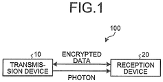
- FIG. 1 is a view illustrating an example of a device configuration of a quantum communication system 100 of the first arrangement.
- the quantum communication system 100 of the first arrangement includes two quantum communication devices (transmission device 10 and reception device 20).
- the transmission device 10 continuously transmits photons indicating quantum bits to the reception device 20.
- a device on a side of transmitting a photon is referred to as the transmission device 10 in the first arrangement.
- the transmission device 10 may have the function of receiving a photon.
- the reception device 20 may have a function of transmitting a photon.
- the transmission device 10 and the reception device 20 transmit and receive encrypted data by using quantum key data. A detail of a method of generating the quantum key data will be described with reference to FIG. 2 .
- FIG. 2 is a view illustrating an example of a functional configuration of the quantum communication system 100 of the first arrangement.
- the quantum communication system 100 of the first arrangement includes the transmission device 10 and the reception device 20.
- the transmission device 10 and the reception device 20 are connected to each other via a quantum communication path 1.
- the quantum communication path 1 is an optical fiber that transmits and receives a photon indicating a quantum bit. Since the quantum communication path 1 transmits and receives very weak light of a single photon, the quantum communication path 1 is easily affected by disturbance.
- the transmission device 10 and the reception device 20 are connected to each other via a classical communication path 2.
- the classical communication path 2 transmits and receives control information for generating quantum key data 105 (209).
- the control information is, for example, partial sift key data 102, an LDPC parameter 207, and syndrome data 104.
- the classical communication path 2 may be in a wired or wireless manner or may be a combination of wired and wireless manners.
- the transmission device 10 includes a transmission unit 11, a sift processing unit 12, a generation unit 13, and a privacy amplification processing unit 14.
- the reception device 20 includes a reception unit 21, a sift processing unit 22, an estimation unit 23, a calculation unit 24, a determination unit 25, a correction unit 26, and a privacy amplification processing unit 27.
- the transmission unit 11 transmits a quantum bit string 101 to the reception unit 21 via the quantum communication path 1.
- Quantum bits included in the quantum bit string 101 are represented by one basis among a plurality of bases using a quantum state of a photon. For example, polarization, a phase, and the like of a photon are used as the basis.
- the reception unit 21 acquires a quantum bit string 201 by receiving the quantum bit string 101 from the transmission unit 11 via the quantum communication path 1.
- the reception unit 21 inputs, into the calculation unit 24, output information 205 of an optical system device used for the processing of acquiring the quantum bit string 201. A detail of the output information 205 will be described later with reference to FIG. 3 .
- the sift processing unit 22 performs sift processing of acquiring sift key data 203 (first sift key data) with respect to the quantum bit string 201 in a unit of a predetermined bit string according to a reference basis randomly selected from a plurality of bases. Then, the sift processing unit 22 inputs the sift key data 203 into the correction unit 26. Moreover, the sift processing unit 22 inputs partial sift key data 202 included in the sift key data 203 into the estimation unit 23.
- the partial sift key data 202 is a bit string, which has a predetermined length and is included in the sift key data 203.
- the sift processing unit 12 of the transmission device 10 acquires sift key data 103 by performing sift processing on the quantum bit string 101. Then, the sift processing unit 12 inputs the sift key data 103 into the generation unit 13 and the privacy amplification processing unit 14. Moreover, the sift processing unit 12 transmits partial sift key data 102 (second partial sift key data) included in the sift key data 103 to the estimation unit 23 via the classical communication path 2.
- the partial sift key data 102 is a bit string, which has a predetermined length and is included in the sift key data 103.
- the estimation unit 23 receives the partial sift key data 102 from the sift processing unit 12 of the transmission device 10 and receives the partial sift key data 202 from the sift processing unit 22.
- the estimation unit 23 specifies positional information of an erroneous bit of the partial sift key data 202 by comparison between the partial sift key data 102 and the partial sift key data 202.
- the estimation unit 23 estimates an estimated error rate 204 of the sift key data 203 according to the positional information of the erroneous bit and an error rate of the partial sift key data 202 acquired from the number of bits of the partial sift key data 202. Then, the estimation unit 23 inputs the estimated error rate 204 into the determination unit 25.
- the calculation unit 24 calculates a margin 206 of the estimated error rate 204 according to the output information 205. A detail of the processing of calculating the margin 206 will be described later with reference to FIG. 4 .
- the calculation unit 24 inputs the margin 206 into the determination unit 25.
- the determination unit 25 receives the estimated error rate 204 from the estimation unit 23 and receives the margin 206 from the calculation unit 24.
- the determination unit 25 determines setting information for error correction processing on the sift key data 203 based on the estimated error rate 204 and the margin 206.
- the setting information may be determined arbitrarily. In the description of the first arrangement, the setting information is the LDPC parameter 207. An example of the LDPC parameter 207 and a detail of a method of determining the LDPC parameter 207 will be described later with reference to FIG. 5 .
- the determination unit 25 inputs the LDPC parameter 207 into the correction unit 26. Moreover, the determination unit 25 transmits the LDPC parameter 207 to the generation unit 13 of the transmission device 10 via the classical communication path 2.
- the generation unit 13 of the transmission device 10 receives the LDPC parameter 207 from the determination unit 25 of the reception device 20 and receives the sift key data 103 from the sift processing unit 12.
- the generation unit 13 generates the syndrome data 104 from the sift key data 103 by using the LDPC parameter 207. Then, the generation unit 13 transmits the syndrome data 104 to the correction unit 26 of the reception device 20 via the classical communication path 2.
- the correction unit 26 of the reception device 20 receives the syndrome data 104 from the generation unit 13 of the transmission device 10, receives the LDPC parameter 207 from the determination unit 25, and receives the sift key data 203 from the sift processing unit 22.
- the correction unit 26 generates corrected key data 208 by performing error correction processing on the sift key data 203 by using the syndrome data 104 and the LDPC parameter 207. Then, the correction unit 26 inputs the corrected key data 208 into the privacy amplification processing unit 27.
- the privacy amplification processing unit 27 When receiving the corrected key data 208 from the correction unit 26, the privacy amplification processing unit 27 generates quantum key data 209 by performing privacy amplification processing on the corrected key data 208.
- the privacy amplification processing is processing of enhancing confidentiality of the quantum key data 209 by compressing the corrected key data 208 and generating the quantum key data 209.
- the privacy amplification processing unit 14 of the transmission device 10 When receiving the sift key data 103 from the sift processing unit 12, the privacy amplification processing unit 14 of the transmission device 10 generates quantum key data 105, which is the same as the quantum key data 209, by performing privacy amplification processing on the sift key data 103.
- FIG. 3 is a view illustrating an example of a hardware configuration of the reception unit 21 of the first arrangement.
- the reception unit 21 of the first arrangement is implemented by a polarization adjuster 221, the Mach-Zehnder interferometer 222, and an optical detector 223.
- the Mach-Zehnder interferometer 222 includes a fiber stretcher 224 and a phase modulator 225.
- a change in a polarization characteristic of an optical fiber (quantum communication path 1) connecting the transmission device 10 and the reception device 20; a change in a phase characteristic of an optical fiber; and deviation in arrival time of a photon are considered.
- the change in a polarization characteristic and the deviation in arrival time of a photon are caused by a change in an external environment such as a temperature of an optical fiber laid section.
- the change in a phase characteristic is caused by a change in a path length of the optical fiber.
- the change in a path length of the optical fiber is caused by a change in a temperature or the like in a room in which the transmission device 10 and the reception device 20 are provided.
- the polarization adjuster 221 adjusts polarization of the optical fiber in order to compensate for the change in a polarization characteristic of the optical fiber.
- the fiber stretcher 224 adjusts a path length of the optical fiber in order to compensate for the change in a phase characteristic of the optical fiber.
- the phase modulator 225 demodulates a phase of a photon modulated by the transmission device 10. While compensating for the deviation in arrival time of a photon by adjusting a detection gate of a photon, the optical detector 223 detects a photon and acquires a plurality of quantum bit strings 201.
- the output information 205 includes an output voltage 231 of the polarization adjuster 221, an output voltage 232 of the fiber stretcher 224, and a detection gate adjustment signal 233.
- the output voltage 231 of the polarization adjuster 221 is a voltage used for control of adjusting polarization of the optical fiber.
- the output voltage 232 of the fiber stretcher 224 is a voltage used for control of adjusting a path length of the optical fiber.
- the detection gate adjustment signal 233 is a voltage used for control of adjusting a detection gate of a photon.
- FIG. 4 is a view illustrating an example of a functional configuration of the calculation unit 24 of the first arrangement.
- the calculation unit 24 of the first arrangement includes a variation amount calculation unit 241 and a margin determination unit 242.
- a variation in the output voltage 231 of the polarization adjuster 221 and a variation in the detection gate adjustment signal 233 correspond to a variation in a polarization characteristic of the optical fiber (quantum communication path 1) and a variation in deviation in arrival time of a photon.
- a variation in the output voltage 232 of the fiber stretcher 224 corresponds to a variation in a phase characteristic of the optical fiber (quantum communication path 1).
- the variation amount calculation unit 241 calculates a variation amount 234 of each of the output voltage 231, the output voltage 232, and the detection gate adjustment signal 233 included in the output information 205.
- the variation amount 234 is, for example, an amount obtained by accumulating absolute values of variation in unit time.
- the variation amount calculation unit 241 inputs the variation amount 234 into the margin determination unit 242.
- the margin determination unit 242 determines the margin 206 based on the variation amount 234.
- the margin determination unit 242 determines the margin 206 according to a ratio of the variation amount 234 to the maximum variation range of voltage determined in the polarization adjuster 221. More specifically, the margin determination unit 242 determines the margin 206 as 5% in a case where the variation amount 234 per minute is 5% or less of the maximum variation range, for example. For example, the margin determination unit 242 determines the margin 206 as 10% in a case where the variation amount 234 per minute is 5% to 10% of the maximum variation range.
- the margin determination unit 242 determines the margin 206 as 15% in a case where the variation amount 234 per minute is 10% to 15% of the maximum variation range. For example, the margin determination unit 242 determines the margin 206 as 20% in a case where the variation amount 234 per minute exceeds 20% of the maximum variation range.
- the margin determination unit 242 determines the margin 206 according to a ratio of the variation amount 234 to the maximum variation range of voltage determined in the fiber stretcher 224.
- the margin determination unit 242 determines the margin 206 according to a ratio of the variation amount 234 to a drive cycle of a detection gate signal of the optical detector 223.
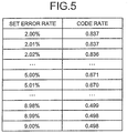
- FIG. 5 is a view illustrating an example of the LDPC parameter 207 of the first arrangement.
- the LDPC parameter 207 is a code rate of an LDPC code is illustrated.
- the determination unit 25 determines the code rate (LDPC parameter 207) according to a set error rate.
- the determination unit 25 determines the code rate (LDPC parameter 207) from the set error rate by using table information illustrated in FIG. 5 , for example.
- the reception unit 21 receives a quantum bit, which is represented by one basis among a plurality of bases using a quantum state of a photon, from the transmission device 10 via the quantum communication path 1, and acquires the quantum bit string 201 including a plurality of received quantum bits.
- the sift processing unit 22 performs sift processing of acquiring the sift key data 203 (first sift key data) with respect to the quantum bit string 201 in a unit of a predetermined bit string according to a reference basis randomly selected from a plurality of bases.
- the determination unit 25 determines setting information (LDPC parameter 207) for error correction processing on the sift key data 203. Then, the correction unit 26 generates the corrected key data 208 by performing the error correction processing with the setting information.
- setting information LDPC parameter 207
- the syndrome data 104 is information related to the sift key data 103, it is necessary to prevent an eavesdropper who may be lurking in the classical communication path 2 from knowing this as much as possible. Thus, it is ideal to determine the LDPC parameter 207 with which it is possible to correct the sift key data 203 and with which a transfer amount of the syndrome data 104 is minimized.
- the quantum communication path 1 affecting an error rate of the sift key data 203 is easily affected by disturbance, a state of the quantum communication path 1 is unstable.
- a true value of the error rate (correct error rate) of the sift key data 203 to be corrected is unknown until correction processing is actually performed. It is ideal that the LDPC parameter 207 corresponding to the true value of the error rate of the sift key data 203 to be corrected is determined.
- the calculation unit 24 calculates the margin 206 from the output information 205 indicating a behavior of an optical system device. That is, the reception device 20 (quantum communication device) of the first arrangement predicts a state of the quantum communication path 1 according to the margin 206 calculated from the output information 205. Then, the determination unit 25 determines the setting information (LDPC parameter 207) in consideration of the margin 206 and the estimated error rate 204. According to the quantum communication system 100 of the first arrangement, it is therefore possible to more appropriately determine the setting information of the error correction processing.
- the second arrangement will be described.
- a description similar to that of the first arrangement will be omitted, and a part different from the first arrangement will be described.
- a method of estimating an estimated error rate 204 is different from that of the first arrangement.
- FIG. 6 is a view illustrating an example of a functional configuration of a quantum communication system 100 of the second arrangement.
- the quantum communication system 100 of the second arrangement includes a transmission device 10 and a reception device 20.
- the transmission device 10 includes a transmission unit 11, a sift processing unit 12, a generation unit 13a, a generation unit 13b, and a privacy amplification processing unit 14.
- the reception device 20 includes a reception unit 21, a sift processing unit 22, an estimation unit 23, a calculation unit 24, a determination unit 25, a correction unit 26a, a correction unit 26b, and a privacy amplification processing unit 27.
- the sift processing unit 12 of the transmission device 10 acquires partial sift key data 102 and sift key data 103 from a quantum bit string 101.
- the sift processing unit 12 inputs the partial sift key data 102 into the generation unit 13a and the sift key data 103 into the generation unit 13b.
- the partial sift key data 102 is not transmitted to the reception device 20 in the second arrangement.
- the partial sift key data 102 may be included in the sift key data 103 to be subjected to an object of privacy amplification processing.
- the generation unit 13a When receiving the partial sift key data 102 from the sift processing unit 12, the generation unit 13a generates partial syndrome data 106 from the partial sift key data 102. Then, the generation unit 13a transmits the partial syndrome data 106 to the correction unit 26a of the reception device 20 via a classical communication path 2.
- the correction unit 26a of the reception device 20 receives the partial syndrome data 106 from the generation unit 13a of the transmission device 10 and receives partial sift key data 202 from the sift processing unit 22.
- the correction unit 26a generates partially corrected key data 210 by performing error correction processing on the partial sift key data 202 (first partial sift key data) by using the partial syndrome data 106. Then, the correction unit 26a inputs the partially corrected key data 210 into the estimation unit 23.
- the partial sift key data 102 is not transmitted to the reception device 20 in the second arrangement.
- the partially corrected key data 210 generated from the partial sift key data 202 corresponding to the partial sift key data 102 may be included in corrected key data 208 to be subjected to the privacy amplification processing.
- the estimation unit 23 receives the partial sift key data 202 from the sift processing unit 22 and receives the partially corrected key data 210 from the correction unit 26a. Based on positional information of an erroneous bit which is acquired by comparison between the partially corrected key data 210 and the partial sift key data 202 (first partial sift key data), the estimation unit 23 estimates an estimated error rate 204 of the sift key data 203.
- generation units 13a and 13b described above may be implemented as one generation unit.
- correction units 26a and 26b described above may be implemented as one correction unit.
- the third arrangement will be described.
- a description similar to that of the first arrangement will be omitted, and a part different from the first arrangement will be described.
- a method of estimating an estimated error rate 204 is different from that of the first arrangement.
- FIG. 7 is a view illustrating an example of a functional configuration of a quantum communication system 100 of the third arrangement.
- the quantum communication system 100 of the third arrangement includes a transmission device 10 and a reception device 20.
- the transmission device 10 includes a transmission unit 11, a sift processing unit 12, a generation unit 13, and a privacy amplification processing unit 14.
- the reception device 20 includes a reception unit 21, a sift processing unit 22, an estimation unit 23, a calculation unit 24, a determination unit 25, a correction unit 26, and a privacy amplification processing unit 27.
- the estimation unit 23 estimates an estimated error rate 204 based on positional information of an erroneous bit acquired by comparison between sift key data 203 (first sift key data) acquired by previous sift processing and corrected key data 208 generated by previous error correction processing. That is, the estimation unit 23 estimates an estimated error rate 204 of sift key data 203 to be subjected to next error correction processing, according to an error rate of the sift key data 203 acquired by the previous sift processing.
- the determination unit 25 may determine an LDPC parameter 207, which has the highest correction capability among usable LDPC parameters 207, as an LDPC parameter 207 used for error correction processing, for example.
- the estimation unit 23 may estimate an estimated error rate 204 according to an error rate of sift key data 203 in the last successful correction.
- FIG. 8 is a view illustrating an example of a configuration of a main part of each of the transmission devices 10 and the reception devices 20 of the first to third arrangements.
- Each of the transmission devices 10 and the reception devices 20 of the first to third arrangements includes a control device 301, a main storage device 302, an auxiliary storage device 303, a display device 304, an input device 305, a quantum communication interface (IF) 306, and a classical communication IF 307.
- IF quantum communication interface
- the control device 301, the main storage device 302, the auxiliary storage device 303, the display device 304, the input device 305, the quantum communication IF 306, and the classical communication IF 307 are connected to each other via a bus 310.
- the control device 301 executes a program read from the auxiliary storage device 303 into the main storage device 302.
- the main storage device 302 is a memory such as a read only memory (ROM) or a random access memory (RAM).
- the auxiliary storage device 303 is a hard disk drive (HDD), a memory card, or the like.
- the display device 304 displays states of the transmission device 10 and the reception device 20, and the like.
- the input device 305 receives an input from a user.
- the quantum communication IF 306 is an interface for connection to the quantum communication path 1.
- the quantum communication IF 306 of the reception device 20 includes a hardware configuration of the reception unit 21 described above (see FIG. 3 ).
- the classical communication IF 307 is an interface for connection to the classical communication path 2.
- Each of the transmission devices 10 and the reception devices 20 of the first to third arrangements can be implemented by an arbitrary device including a general-purpose computer or the like as long as the hardware configuration in FIG. 8 is included.
- a program executed by each of the transmission devices 10 and the reception devices 20 of the first to third arrangements is provided as a computer program product while being stored as a file in an installable format or an executable format in a computer-readable storage medium such as a CD-ROM, a memory card, a CD-R, or a digital versatile disc (DVD).
- a computer-readable storage medium such as a CD-ROM, a memory card, a CD-R, or a digital versatile disc (DVD).
- each of the transmission devices 10 and the reception devices 20 of the first to third arrangements may be stored in a computer connected to a network such as the Internet and may be provided by being downloaded via the network.
- each of the transmission devices 10 and the reception devices 20 of the first to third arrangements may be provided via a network such as the Internet without being downloaded.
- each of the transmission devices 10 and the reception devices 20 of the first to third arrangements may be previously incorporated in a ROM or the like and provided.
- the program executed by each of the transmission devices 10 and the reception devices 20 of the first to third arrangements has a module configuration including a function that can be implemented by the program among functional configurations of the transmission device 10 and the reception device 20 of each of the first to third arrangements.
- the control device 301 reads a program from a storage medium such as the auxiliary storage device 303 and executes the program, whereby a function implemented by the program is loaded into the main storage device 302. That is, the function implemented by the program is generated on the main storage device 302.
- a part or a whole of functions of the transmission device 10 and the reception device 20 of each of the first to third arrangements may be implemented by hardware such as an integrated circuit (IC).
- the IC is, for example, a processor that executes dedicated processing.
- each processor may implement one of the functions or may implement two or more of the functions.
- operation forms of the transmission device 10 and the reception device 20 of each of the first to third arrangements may be arbitrary.
- the transmission device 10 and the reception device 20 of each of the first to third arrangements may be operated as devices included in a cloud system on a network, for example.
- a quantum communication device is adapted to correct first sift key data acquired by performing sift processing with respect to a quantum bit string received from a transmission device via a quantum communication path.
- the quantum communication device includes a determination unit and a correction unit.
- the determination unit is configured to determine setting information of error correction processing on the first sift key data from an estimated error rate of the first sift key data and a margin of the estimated error rate.
- the correction unit is configured to generate corrected key data by performing the error correction processing using the setting information.
- the quantum communication device further includes an estimation unit configured to estimate the estimated error rate by comparison between first partial sift key data included in the first sift key data and second partial sift key data included in second sift key data acquired by the sift processing by the transmission device.
- the correction unit generates partially corrected key data by performing the error correction processing on first partial sift key data included in the first sift key data.
- the quantum communication device further comprises an estimation unit configured to estimate the estimated error rate by comparison between the partially corrected key data and the first partial sift key data.
- Example 4 The quantum communication device according to Example 1 further includes an estimation unit configured to estimate the estimated error rate by comparison between the first sift key data acquired by previous sift processing and the corrected key data generated by previous error correction processing.
- the quantum communication device further includes a calculation unit configured to calculate the margin based on output information of an optical system device used to receive the quantum bit string.
- Example 6 In the quantum communication device according to Example 5, the optical system device is a polarization adjuster.
- the calculation unit calculates the margin based on a variation amount of an output voltage of the polarization adjuster.
- Example 7 In the quantum communication device according to Example 5, the optical system device is a fiber stretcher.
- the calculation unit calculates the margin based on a variation amount of an output voltage of the fiber stretcher.
- Example 8 In the quantum communication device according to Example 5, the optical system device is an optical detector.
- the calculation unit calculates the margin based on a variation amount of a detection gate adjustment signal of the optical detector.
- a quantum communication system includes a transmission device and a reception device.
- the reception device is configured to correct first sift key data acquired by performing sift processing with respect to a quantum bit string received from the transmission device via a quantum communication path.
- the reception device includes a determination unit and a correction unit.
- the determination unit is configured to determine setting information of error correction processing on the first sift key data from an estimated error rate of the first sift key data and a margin of the estimated error rate.
- the correction unit is configured to generate corrected key data by performing the error correction processing using the setting information.
- Example 10 A quantum communication method is used for a quantum communication device configured to correct first sift key data acquired by performing sift processing with respect to a quantum bit string received from a transmission device via a quantum communication path.
- the method includes: determining setting information of error correction processing on the first sift key data from an estimated error rate of the first sift key data and a margin of the estimated error rate; and generating corrected key data by performing the error correction processing using the setting information.
- a quantum communication device includes a reception unit, a sift processing unit, a determination unit, and a correction unit.
- the reception unit is configured to receive a quantum bit, which is represented by one basis among a plurality of bases using a quantum state of a photon, from a transmission device via a quantum communication path and to acquire a quantum bit string including a plurality of received quantum bits.
- the sift processing unit is configured to perform sift processing of acquiring first sift key data with reference to the quantum bit string in a unit of a predetermined bit string according to a reference basis randomly selected from the plurality of bases.
- the determination unit is configured to determine setting information of error correction processing on the first sift key data from an estimated error rate of the first sift key data and a margin of the estimated error rate.
- the correction unit is configured to generate corrected key data by performing the error correction processing with the setting information.
- a quantum communication system includes a transmission device and a reception device connected to each other via a quantum communication path.
- the reception device includes a reception unit, a sift processing unit, a determination unit, and a correction unit.
- the reception unit is configured to receive a quantum bit, which is represented by one basis among a plurality of bases using a quantum state of a photon, from the transmission device via the quantum communication path and to acquire a quantum bit string including a plurality of received quantum bits.
- the sift processing unit is configured to perform sift processing of acquiring first sift key data with reference to the quantum bit string in a unit of a predetermined bit string according to a reference basis randomly selected from the plurality of bases.
- the determination unit is configured to determine setting information of error correction processing on the first sift key data from an estimated error rate of the first sift key data and a margin of the estimated error rate.
- the correction unit is configured to generate corrected key data by performing the error correction processing with the setting information.
- a quantum communication method includes: receiving a quantum bit, which is represented by one basis among a plurality of bases using a quantum state of a photon, from a transmission device via a quantum communication path and acquiring a quantum bit string including a plurality of received quantum bits; performing sift processing of acquiring first sift key data with reference to the quantum bit string in a unit of a predetermined bit string according to a reference basis randomly selected from the plurality of bases; determining setting information of error correction processing on the first sift key data from an estimated error rate of the first sift key data and a margin of the estimated error rate; and generating corrected key data by performing the error correction processing with the setting information.
Landscapes
- Engineering & Computer Science (AREA)
- Computer Security & Cryptography (AREA)
- Computer Networks & Wireless Communication (AREA)
- Signal Processing (AREA)
- Theoretical Computer Science (AREA)
- Physics & Mathematics (AREA)
- Electromagnetism (AREA)
- Computing Systems (AREA)
- Optical Communication System (AREA)
Abstract
Description
- The present disclosure relates to a quantum communication device, a quantum communication system, and a quantum communication method.
- A low density parity check (LDPC) code attracts attention as an error correction code having an error correction capability very close to the Shannon limit that is the theoretical limit value of an information transmission rate. Thus, for example, it is actively considered to implement an LDPC decoder as hardware in fields of communication, storage system, and the like.
-
-
FIG. 1 is a view illustrating an example of a device configuration of a quantum communication system of a first arrangement; -
FIG. 2 is a view illustrating an example of a functional configuration of the quantum communication system of the first arrangement; -
FIG. 3 is a view illustrating an example of a hardware configuration of a reception unit of the first arrangement; -
FIG. 4 is a view illustrating an example of a functional configuration of a calculation unit of the first arrangement; -
FIG. 5 is a view illustrating an example of an LDPC parameter of the first arrangement; -
FIG. 6 is a view illustrating an example of a functional configuration of a quantum communication system of a second arrangement; -
FIG. 7 is a view illustrating an example of a functional configuration of a quantum communication system of a third arrangement; and -
FIG. 8 is a view illustrating an example of a hardware configuration of a main part of each of transmission devices and reception devices of the first to third arrangements. - According to an arrangement, a quantum communication device is adapted to correct first sift key data acquired by performing sift processing with respect to a quantum bit string received from a transmission device via a quantum communication path. The quantum communication device includes a determination unit and a correction unit. The determination unit determines setting information of error correction processing on the first sift key data from an estimated error rate of the first sift key data and a margin of the estimated error rate. The correction unit generates corrected key data by performing the error correction processing with the setting information.
- In the following, arrangements of a quantum communication device, a quantum communication system, and a quantum communication method will be described in detail with reference to the attached drawings.
- First, the first arrangement will be described.
-
FIG. 1 is a view illustrating an example of a device configuration of aquantum communication system 100 of the first arrangement. Thequantum communication system 100 of the first arrangement includes two quantum communication devices (transmission device 10 and reception device 20). The transmission device 10 continuously transmits photons indicating quantum bits to thereception device 20. Note that for convenience of description, a device on a side of transmitting a photon is referred to as the transmission device 10 in the first arrangement. However, the transmission device 10 may have the function of receiving a photon. Similarly, thereception device 20 may have a function of transmitting a photon. - The transmission device 10 and the
reception device 20 transmit and receive encrypted data by using quantum key data. A detail of a method of generating the quantum key data will be described with reference toFIG. 2 . -
FIG. 2 is a view illustrating an example of a functional configuration of thequantum communication system 100 of the first arrangement. Thequantum communication system 100 of the first arrangement includes the transmission device 10 and thereception device 20. - The transmission device 10 and the
reception device 20 are connected to each other via aquantum communication path 1. Thequantum communication path 1 is an optical fiber that transmits and receives a photon indicating a quantum bit. Since thequantum communication path 1 transmits and receives very weak light of a single photon, thequantum communication path 1 is easily affected by disturbance. - The transmission device 10 and the
reception device 20 are connected to each other via a classical communication path 2. The classical communication path 2 transmits and receives control information for generating quantum key data 105 (209). In the example inFIG. 2 , the control information is, for example, partialsift key data 102, anLDPC parameter 207, andsyndrome data 104. The classical communication path 2 may be in a wired or wireless manner or may be a combination of wired and wireless manners. - The transmission device 10 includes a transmission unit 11, a
sift processing unit 12, ageneration unit 13, and a privacy amplification processing unit 14. - The
reception device 20 includes areception unit 21, a sift processing unit 22, anestimation unit 23, acalculation unit 24, adetermination unit 25, acorrection unit 26, and a privacyamplification processing unit 27. - The transmission unit 11 transmits a
quantum bit string 101 to thereception unit 21 via thequantum communication path 1. Quantum bits included in thequantum bit string 101 are represented by one basis among a plurality of bases using a quantum state of a photon. For example, polarization, a phase, and the like of a photon are used as the basis. - The
reception unit 21 acquires aquantum bit string 201 by receiving thequantum bit string 101 from the transmission unit 11 via thequantum communication path 1. Thereception unit 21 inputs, into thecalculation unit 24,output information 205 of an optical system device used for the processing of acquiring thequantum bit string 201. A detail of theoutput information 205 will be described later with reference toFIG. 3 . - The sift processing unit 22 performs sift processing of acquiring sift key data 203 (first sift key data) with respect to the
quantum bit string 201 in a unit of a predetermined bit string according to a reference basis randomly selected from a plurality of bases. Then, the sift processing unit 22 inputs thesift key data 203 into thecorrection unit 26. Moreover, the sift processing unit 22 inputs partialsift key data 202 included in thesift key data 203 into theestimation unit 23. The partialsift key data 202 is a bit string, which has a predetermined length and is included in thesift key data 203. - The
sift processing unit 12 of the transmission device 10 acquiressift key data 103 by performing sift processing on thequantum bit string 101. Then, thesift processing unit 12 inputs thesift key data 103 into thegeneration unit 13 and the privacy amplification processing unit 14. Moreover, thesift processing unit 12 transmits partial sift key data 102 (second partial sift key data) included in thesift key data 103 to theestimation unit 23 via the classical communication path 2. The partialsift key data 102 is a bit string, which has a predetermined length and is included in thesift key data 103. - The
estimation unit 23 receives the partialsift key data 102 from thesift processing unit 12 of the transmission device 10 and receives the partialsift key data 202 from the sift processing unit 22. Theestimation unit 23 specifies positional information of an erroneous bit of the partialsift key data 202 by comparison between the partialsift key data 102 and the partialsift key data 202. Theestimation unit 23 estimates an estimatederror rate 204 of thesift key data 203 according to the positional information of the erroneous bit and an error rate of the partialsift key data 202 acquired from the number of bits of the partialsift key data 202. Then, theestimation unit 23 inputs the estimatederror rate 204 into thedetermination unit 25. - When receiving the
output information 205 from thereception unit 21, thecalculation unit 24 calculates amargin 206 of the estimatederror rate 204 according to theoutput information 205. A detail of the processing of calculating themargin 206 will be described later with reference toFIG. 4 . Thecalculation unit 24 inputs themargin 206 into thedetermination unit 25. - The
determination unit 25 receives the estimatederror rate 204 from theestimation unit 23 and receives themargin 206 from thecalculation unit 24. Thedetermination unit 25 determines setting information for error correction processing on the siftkey data 203 based on the estimatederror rate 204 and themargin 206. The setting information may be determined arbitrarily. In the description of the first arrangement, the setting information is theLDPC parameter 207. An example of theLDPC parameter 207 and a detail of a method of determining theLDPC parameter 207 will be described later with reference toFIG. 5 . Thedetermination unit 25 inputs theLDPC parameter 207 into thecorrection unit 26. Moreover, thedetermination unit 25 transmits theLDPC parameter 207 to thegeneration unit 13 of the transmission device 10 via the classical communication path 2. - The
generation unit 13 of the transmission device 10 receives theLDPC parameter 207 from thedetermination unit 25 of thereception device 20 and receives the siftkey data 103 from the sift processingunit 12. Thegeneration unit 13 generates thesyndrome data 104 from the siftkey data 103 by using theLDPC parameter 207. Then, thegeneration unit 13 transmits thesyndrome data 104 to thecorrection unit 26 of thereception device 20 via the classical communication path 2. - The
correction unit 26 of thereception device 20 receives thesyndrome data 104 from thegeneration unit 13 of the transmission device 10, receives theLDPC parameter 207 from thedetermination unit 25, and receives the siftkey data 203 from the sift processing unit 22. Thecorrection unit 26 generates correctedkey data 208 by performing error correction processing on the siftkey data 203 by using thesyndrome data 104 and theLDPC parameter 207. Then, thecorrection unit 26 inputs the correctedkey data 208 into the privacyamplification processing unit 27. - When receiving the corrected
key data 208 from thecorrection unit 26, the privacyamplification processing unit 27 generates quantumkey data 209 by performing privacy amplification processing on the correctedkey data 208. The privacy amplification processing is processing of enhancing confidentiality of the quantumkey data 209 by compressing the correctedkey data 208 and generating the quantumkey data 209. - When receiving the sift
key data 103 from the sift processingunit 12, the privacy amplification processing unit 14 of the transmission device 10 generates quantumkey data 105, which is the same as the quantumkey data 209, by performing privacy amplification processing on the siftkey data 103. - Next, a detail of the
output information 205 of an optical system device used in thereception unit 21 will be described with reference toFIG. 3 . -
FIG. 3 is a view illustrating an example of a hardware configuration of thereception unit 21 of the first arrangement. Thereception unit 21 of the first arrangement is implemented by apolarization adjuster 221, the Mach-Zehnder interferometer 222, and anoptical detector 223. The Mach-Zehnder interferometer 222 includes afiber stretcher 224 and aphase modulator 225. - As factors that make quantum cryptographic communication unstable, the following three factors are considered: a change in a polarization characteristic of an optical fiber (quantum communication path 1) connecting the transmission device 10 and the
reception device 20; a change in a phase characteristic of an optical fiber; and deviation in arrival time of a photon are considered. The change in a polarization characteristic and the deviation in arrival time of a photon are caused by a change in an external environment such as a temperature of an optical fiber laid section. The change in a phase characteristic is caused by a change in a path length of the optical fiber. The change in a path length of the optical fiber is caused by a change in a temperature or the like in a room in which the transmission device 10 and thereception device 20 are provided. When the change in a polarization characteristic of the optical fiber, the change in a phase characteristic of the optical fiber, and the deviation in arrival time of a photon are caused, an error rate of thequantum communication path 1 is increased. - The
polarization adjuster 221 adjusts polarization of the optical fiber in order to compensate for the change in a polarization characteristic of the optical fiber. Thefiber stretcher 224 adjusts a path length of the optical fiber in order to compensate for the change in a phase characteristic of the optical fiber. Thephase modulator 225 demodulates a phase of a photon modulated by the transmission device 10. While compensating for the deviation in arrival time of a photon by adjusting a detection gate of a photon, theoptical detector 223 detects a photon and acquires a plurality of quantum bit strings 201. - The
output information 205 includes anoutput voltage 231 of thepolarization adjuster 221, anoutput voltage 232 of thefiber stretcher 224, and a detectiongate adjustment signal 233. Theoutput voltage 231 of thepolarization adjuster 221 is a voltage used for control of adjusting polarization of the optical fiber. Theoutput voltage 232 of thefiber stretcher 224 is a voltage used for control of adjusting a path length of the optical fiber. The detectiongate adjustment signal 233 is a voltage used for control of adjusting a detection gate of a photon. - Next, a detail of the processing of calculating the
margin 206 will be described with reference toFIG. 4 . -
FIG. 4 is a view illustrating an example of a functional configuration of thecalculation unit 24 of the first arrangement. Thecalculation unit 24 of the first arrangement includes a variationamount calculation unit 241 and amargin determination unit 242. - A variation in the
output voltage 231 of thepolarization adjuster 221 and a variation in the detectiongate adjustment signal 233 correspond to a variation in a polarization characteristic of the optical fiber (quantum communication path 1) and a variation in deviation in arrival time of a photon. Thus, the larger the variation in theoutput voltage 231 of thepolarization adjuster 221 and the variation in the detectiongate adjustment signal 233 is, the more unstable a state of thequantum communication path 1 becomes. - A variation in the
output voltage 232 of thefiber stretcher 224 corresponds to a variation in a phase characteristic of the optical fiber (quantum communication path 1). The lager the variation in theoutput voltage 232 of thefiber stretcher 224 is, the more unstable a state of thequantum communication path 1 becomes. - In summary, the larger the variation in the output information 205 (
output voltage 231,output voltage 232, and detection gate adjustment signal 233) is, the more unstable a state of thequantum communication path 1 becomes. - When receiving the
output information 205 from thereception unit 21, the variationamount calculation unit 241 calculates avariation amount 234 of each of theoutput voltage 231, theoutput voltage 232, and the detectiongate adjustment signal 233 included in theoutput information 205. Thevariation amount 234 is, for example, an amount obtained by accumulating absolute values of variation in unit time. The variationamount calculation unit 241 inputs thevariation amount 234 into themargin determination unit 242. - When receiving the
variation amount 234 from the variationamount calculation unit 241, themargin determination unit 242 determines themargin 206 based on thevariation amount 234. - For example, in a case where the
variation amount 234 is a variation amount of theoutput voltage 231 of thepolarization adjuster 221, themargin determination unit 242 determines themargin 206 according to a ratio of thevariation amount 234 to the maximum variation range of voltage determined in thepolarization adjuster 221. More specifically, themargin determination unit 242 determines themargin 206 as 5% in a case where thevariation amount 234 per minute is 5% or less of the maximum variation range, for example. For example, themargin determination unit 242 determines themargin 206 as 10% in a case where thevariation amount 234 per minute is 5% to 10% of the maximum variation range. For example, themargin determination unit 242 determines themargin 206 as 15% in a case where thevariation amount 234 per minute is 10% to 15% of the maximum variation range. For example, themargin determination unit 242 determines themargin 206 as 20% in a case where thevariation amount 234 per minute exceeds 20% of the maximum variation range. - For example, in a case where the
variation amount 234 is a variation amount of theoutput voltage 232 of thefiber stretcher 224, themargin determination unit 242 determines themargin 206 according to a ratio of thevariation amount 234 to the maximum variation range of voltage determined in thefiber stretcher 224. - For example, in a case where the
variation amount 234 is a variation amount of the detectiongate adjustment signal 233, themargin determination unit 242 determines themargin 206 according to a ratio of thevariation amount 234 to a drive cycle of a detection gate signal of theoptical detector 223. - Next, an example of the
LDPC parameter 207 and a detail of a method of determining theLDPC parameter 207 will be described with reference toFIG. 5 . -
FIG. 5 is a view illustrating an example of theLDPC parameter 207 of the first arrangement. In the example inFIG. 5 , a case where theLDPC parameter 207 is a code rate of an LDPC code is illustrated. Thedetermination unit 25 determines the code rate (LDPC parameter 207) according to a set error rate. The set error rate is calculated from the estimatederror rate 204 and themargin 206. For example, in a case where the estimatederror rate 204 is 2% and themargin 206 is 20%, thedetermination unit 25 determines the set error rate as 2.4% (= 2×1.2). Thedetermination unit 25 determines the code rate (LDPC parameter 207) from the set error rate by using table information illustrated inFIG. 5 , for example. - As described above, in the reception device 20 (quantum communication device) of the first arrangement, the
reception unit 21 receives a quantum bit, which is represented by one basis among a plurality of bases using a quantum state of a photon, from the transmission device 10 via thequantum communication path 1, and acquires thequantum bit string 201 including a plurality of received quantum bits. The sift processing unit 22 performs sift processing of acquiring the sift key data 203 (first sift key data) with respect to thequantum bit string 201 in a unit of a predetermined bit string according to a reference basis randomly selected from a plurality of bases. From the estimatederror rate 204 of the siftkey data 203 and themargin 206 of the estimatederror rate 204, thedetermination unit 25 determines setting information (LDPC parameter 207) for error correction processing on the siftkey data 203. Then, thecorrection unit 26 generates the correctedkey data 208 by performing the error correction processing with the setting information. - In the error correction processing in quantum cryptographic communication, it is necessary to transfer the
syndrome data 104 via the classical communication path 2. Since thesyndrome data 104 is information related to the siftkey data 103, it is necessary to prevent an eavesdropper who may be lurking in the classical communication path 2 from knowing this as much as possible. Thus, it is ideal to determine theLDPC parameter 207 with which it is possible to correct the siftkey data 203 and with which a transfer amount of thesyndrome data 104 is minimized. However, since thequantum communication path 1 affecting an error rate of the siftkey data 203 is easily affected by disturbance, a state of thequantum communication path 1 is unstable. Moreover, a true value of the error rate (correct error rate) of the siftkey data 203 to be corrected is unknown until correction processing is actually performed. It is ideal that theLDPC parameter 207 corresponding to the true value of the error rate of the siftkey data 203 to be corrected is determined. - In the reception device 20 (quantum communication device) of the first arrangement, the
calculation unit 24 calculates themargin 206 from theoutput information 205 indicating a behavior of an optical system device. That is, the reception device 20 (quantum communication device) of the first arrangement predicts a state of thequantum communication path 1 according to themargin 206 calculated from theoutput information 205. Then, thedetermination unit 25 determines the setting information (LDPC parameter 207) in consideration of themargin 206 and the estimatederror rate 204. According to thequantum communication system 100 of the first arrangement, it is therefore possible to more appropriately determine the setting information of the error correction processing. - Next, the second arrangement will be described. In a description of the second arrangement, a description similar to that of the first arrangement will be omitted, and a part different from the first arrangement will be described. In the second arrangement, a method of estimating an estimated
error rate 204 is different from that of the first arrangement. -
FIG. 6 is a view illustrating an example of a functional configuration of aquantum communication system 100 of the second arrangement. Thequantum communication system 100 of the second arrangement includes a transmission device 10 and areception device 20. - The transmission device 10 includes a transmission unit 11, a sift
processing unit 12, ageneration unit 13a, a generation unit 13b, and a privacy amplification processing unit 14. - The
reception device 20 includes areception unit 21, a sift processing unit 22, anestimation unit 23, acalculation unit 24, adetermination unit 25, a correction unit 26a, acorrection unit 26b, and a privacyamplification processing unit 27. - Similarly to the first arrangement, the sift processing
unit 12 of the transmission device 10 acquires partial siftkey data 102 and siftkey data 103 from aquantum bit string 101. The siftprocessing unit 12 inputs the partial siftkey data 102 into thegeneration unit 13a and the siftkey data 103 into the generation unit 13b. - Note that the partial sift
key data 102 is not transmitted to thereception device 20 in the second arrangement. Thus, the partial siftkey data 102 may be included in the siftkey data 103 to be subjected to an object of privacy amplification processing. - When receiving the partial sift
key data 102 from the sift processingunit 12, thegeneration unit 13a generatespartial syndrome data 106 from the partial siftkey data 102. Then, thegeneration unit 13a transmits thepartial syndrome data 106 to the correction unit 26a of thereception device 20 via a classical communication path 2. - Since an operation of the generation unit 13b is the same as that of the
generation unit 13 of the first arrangement, a description thereof is omitted. - The correction unit 26a of the
reception device 20 receives thepartial syndrome data 106 from thegeneration unit 13a of the transmission device 10 and receives partial siftkey data 202 from the sift processing unit 22. The correction unit 26a generates partially correctedkey data 210 by performing error correction processing on the partial sift key data 202 (first partial sift key data) by using thepartial syndrome data 106. Then, the correction unit 26a inputs the partially correctedkey data 210 into theestimation unit 23. - Note that the partial sift
key data 102 is not transmitted to thereception device 20 in the second arrangement. Thus, the partially correctedkey data 210 generated from the partial siftkey data 202 corresponding to the partial siftkey data 102 may be included in correctedkey data 208 to be subjected to the privacy amplification processing. - The
estimation unit 23 receives the partial siftkey data 202 from the sift processing unit 22 and receives the partially correctedkey data 210 from the correction unit 26a. Based on positional information of an erroneous bit which is acquired by comparison between the partially correctedkey data 210 and the partial sift key data 202 (first partial sift key data), theestimation unit 23 estimates an estimatederror rate 204 of the siftkey data 203. - Since an operation of the
correction unit 26b is the same as that of thecorrection unit 26 of the first arrangement, a description thereof is omitted. - Note that the
generation units 13a and 13b described above may be implemented as one generation unit. Similarly, thecorrection units 26a and 26b described above may be implemented as one correction unit. - As described above, according to the
quantum communication system 100 of the second arrangement, similarly to a case of the first arrangement, setting information of the error correction processing can be more appropriately determined. - Next, the third arrangement will be described. In the description of the third arrangement, a description similar to that of the first arrangement will be omitted, and a part different from the first arrangement will be described. In the third arrangement, a method of estimating an estimated
error rate 204 is different from that of the first arrangement. -
FIG. 7 is a view illustrating an example of a functional configuration of aquantum communication system 100 of the third arrangement. Thequantum communication system 100 of the third arrangement includes a transmission device 10 and areception device 20. - The transmission device 10 includes a transmission unit 11, a sift
processing unit 12, ageneration unit 13, and a privacy amplification processing unit 14. - The
reception device 20 includes areception unit 21, a sift processing unit 22, anestimation unit 23, acalculation unit 24, adetermination unit 25, acorrection unit 26, and a privacyamplification processing unit 27. - The
estimation unit 23 estimates an estimatederror rate 204 based on positional information of an erroneous bit acquired by comparison between sift key data 203 (first sift key data) acquired by previous sift processing and correctedkey data 208 generated by previous error correction processing. That is, theestimation unit 23 estimates an estimatederror rate 204 of siftkey data 203 to be subjected to next error correction processing, according to an error rate of the siftkey data 203 acquired by the previous sift processing. - Note that in a case where preceding error correction processing fails, the
determination unit 25 may determine anLDPC parameter 207, which has the highest correction capability amongusable LDPC parameters 207, as anLDPC parameter 207 used for error correction processing, for example. Alternatively, for example, theestimation unit 23 may estimate an estimatederror rate 204 according to an error rate of siftkey data 203 in the last successful correction. - As described above, according to the
quantum communication system 100 of the third arrangement, similarly to a case of the first arrangement, setting information of the error correction processing can be more appropriately determined. - Finally, an example of hardware configurations of the transmission device 10 and the
reception device 20 of each of the first to third arrangements will be described. -
FIG. 8 is a view illustrating an example of a configuration of a main part of each of the transmission devices 10 and thereception devices 20 of the first to third arrangements. Each of the transmission devices 10 and thereception devices 20 of the first to third arrangements includes acontrol device 301, amain storage device 302, anauxiliary storage device 303, adisplay device 304, aninput device 305, a quantum communication interface (IF) 306, and a classical communication IF 307. - The
control device 301, themain storage device 302, theauxiliary storage device 303, thedisplay device 304, theinput device 305, the quantum communication IF 306, and the classical communication IF 307 are connected to each other via abus 310. - The
control device 301 executes a program read from theauxiliary storage device 303 into themain storage device 302. Themain storage device 302 is a memory such as a read only memory (ROM) or a random access memory (RAM). Theauxiliary storage device 303 is a hard disk drive (HDD), a memory card, or the like. - The
display device 304 displays states of the transmission device 10 and thereception device 20, and the like. Theinput device 305 receives an input from a user. - The quantum communication IF 306 is an interface for connection to the
quantum communication path 1. The quantum communication IF 306 of thereception device 20 includes a hardware configuration of thereception unit 21 described above (seeFIG. 3 ). The classical communication IF 307 is an interface for connection to the classical communication path 2. - Each of the transmission devices 10 and the
reception devices 20 of the first to third arrangements can be implemented by an arbitrary device including a general-purpose computer or the like as long as the hardware configuration inFIG. 8 is included. - A program executed by each of the transmission devices 10 and the
reception devices 20 of the first to third arrangements is provided as a computer program product while being stored as a file in an installable format or an executable format in a computer-readable storage medium such as a CD-ROM, a memory card, a CD-R, or a digital versatile disc (DVD). - Also, the program executed by each of the transmission devices 10 and the
reception devices 20 of the first to third arrangements may be stored in a computer connected to a network such as the Internet and may be provided by being downloaded via the network. - Also, the program executed by each of the transmission devices 10 and the
reception devices 20 of the first to third arrangements may be provided via a network such as the Internet without being downloaded. - Also, the program executed by each of the transmission devices 10 and the
reception devices 20 of the first to third arrangements may be previously incorporated in a ROM or the like and provided. - The program executed by each of the transmission devices 10 and the
reception devices 20 of the first to third arrangements has a module configuration including a function that can be implemented by the program among functional configurations of the transmission device 10 and thereception device 20 of each of the first to third arrangements. - The
control device 301 reads a program from a storage medium such as theauxiliary storage device 303 and executes the program, whereby a function implemented by the program is loaded into themain storage device 302. That is, the function implemented by the program is generated on themain storage device 302. - A part or a whole of functions of the transmission device 10 and the
reception device 20 of each of the first to third arrangements may be implemented by hardware such as an integrated circuit (IC). The IC is, for example, a processor that executes dedicated processing. - In a case where functions are implemented with a plurality of processors, each processor may implement one of the functions or may implement two or more of the functions.
- Also, operation forms of the transmission device 10 and the
reception device 20 of each of the first to third arrangements may be arbitrary. The transmission device 10 and thereception device 20 of each of the first to third arrangements may be operated as devices included in a cloud system on a network, for example. - While certain arrangements have been described, these arrangements have been presented by way of example only, and are not intended to limit the scope of the claims. Indeed, the devices described herein may be embodied in a variety of other forms; furthermore various omissions, substitutions and changes in the form of the devices described herein may be made.
- Example 1. A quantum communication device is adapted to correct first sift key data acquired by performing sift processing with respect to a quantum bit string received from a transmission device via a quantum communication path. The quantum communication device includes a determination unit and a correction unit. The determination unit is configured to determine setting information of error correction processing on the first sift key data from an estimated error rate of the first sift key data and a margin of the estimated error rate. The correction unit is configured to generate corrected key data by performing the error correction processing using the setting information.
- Example 2. The quantum communication device according to Example 1 further includes an estimation unit configured to estimate the estimated error rate by comparison between first partial sift key data included in the first sift key data and second partial sift key data included in second sift key data acquired by the sift processing by the transmission device.
- Example 3. In the quantum communication device according to Example 1, the correction unit generates partially corrected key data by performing the error correction processing on first partial sift key data included in the first sift key data. The quantum communication device further comprises an estimation unit configured to estimate the estimated error rate by comparison between the partially corrected key data and the first partial sift key data.
- Example 4. The quantum communication device according to Example 1 further includes an estimation unit configured to estimate the estimated error rate by comparison between the first sift key data acquired by previous sift processing and the corrected key data generated by previous error correction processing.
- Example 5. The quantum communication device according to Example 1 further includes a calculation unit configured to calculate the margin based on output information of an optical system device used to receive the quantum bit string.
- Example 6. In the quantum communication device according to Example 5, the optical system device is a polarization adjuster. The calculation unit calculates the margin based on a variation amount of an output voltage of the polarization adjuster.
- Example 7. In the quantum communication device according to Example 5, the optical system device is a fiber stretcher. The calculation unit calculates the margin based on a variation amount of an output voltage of the fiber stretcher.
- Example 8. In the quantum communication device according to Example 5, the optical system device is an optical detector. The calculation unit calculates the margin based on a variation amount of a detection gate adjustment signal of the optical detector.
- Example 9. A quantum communication system includes a transmission device and a reception device. The reception device is configured to correct first sift key data acquired by performing sift processing with respect to a quantum bit string received from the transmission device via a quantum communication path. The reception device includes a determination unit and a correction unit. The determination unit is configured to determine setting information of error correction processing on the first sift key data from an estimated error rate of the first sift key data and a margin of the estimated error rate. The correction unit is configured to generate corrected key data by performing the error correction processing using the setting information.
- Example 10. A quantum communication method is used for a quantum communication device configured to correct first sift key data acquired by performing sift processing with respect to a quantum bit string received from a transmission device via a quantum communication path. The method includes: determining setting information of error correction processing on the first sift key data from an estimated error rate of the first sift key data and a margin of the estimated error rate; and generating corrected key data by performing the error correction processing using the setting information.
- Example 11. A quantum communication device includes a reception unit, a sift processing unit, a determination unit, and a correction unit. The reception unit is configured to receive a quantum bit, which is represented by one basis among a plurality of bases using a quantum state of a photon, from a transmission device via a quantum communication path and to acquire a quantum bit string including a plurality of received quantum bits. The sift processing unit is configured to perform sift processing of acquiring first sift key data with reference to the quantum bit string in a unit of a predetermined bit string according to a reference basis randomly selected from the plurality of bases. The determination unit is configured to determine setting information of error correction processing on the first sift key data from an estimated error rate of the first sift key data and a margin of the estimated error rate. The correction unit is configured to generate corrected key data by performing the error correction processing with the setting information.
- Example 12. A quantum communication system includes a transmission device and a reception device connected to each other via a quantum communication path. The reception device includes a reception unit, a sift processing unit, a determination unit, and a correction unit. The reception unit is configured to receive a quantum bit, which is represented by one basis among a plurality of bases using a quantum state of a photon, from the transmission device via the quantum communication path and to acquire a quantum bit string including a plurality of received quantum bits. The sift processing unit is configured to perform sift processing of acquiring first sift key data with reference to the quantum bit string in a unit of a predetermined bit string according to a reference basis randomly selected from the plurality of bases. The determination unit is configured to determine setting information of error correction processing on the first sift key data from an estimated error rate of the first sift key data and a margin of the estimated error rate. The correction unit is configured to generate corrected key data by performing the error correction processing with the setting information.
- Example 13. A quantum communication method includes: receiving a quantum bit, which is represented by one basis among a plurality of bases using a quantum state of a photon, from a transmission device via a quantum communication path and acquiring a quantum bit string including a plurality of received quantum bits; performing sift processing of acquiring first sift key data with reference to the quantum bit string in a unit of a predetermined bit string according to a reference basis randomly selected from the plurality of bases; determining setting information of error correction processing on the first sift key data from an estimated error rate of the first sift key data and a margin of the estimated error rate; and generating corrected key data by performing the error correction processing with the setting information.
Claims (10)
- A quantum communication device (20) adapted to correct first sift key data (203) acquired by performing sift processing with respect to a quantum bit string (201) received from a transmission device (10) via a quantum communication path (1), the device (20) comprising:a determination unit (25) configured to determine setting information (207) of error correction processing on the first sift key data (203) from an estimated error rate (204) of the first sift key data (203) and a margin (206) of the estimated error rate (204); anda correction unit (26) configured to generate corrected key data (208) by performing the error correction processing using the setting information (207).
- The quantum communication device (20) according to claim 1, further comprising:an estimation unit (23) configured to estimate the estimated error rate (204) by comparison between first partial sift key data (202) included in the first sift key data (203) and second partial sift key data (102) included in second sift key data (103) acquired by the sift processing by the transmission device (10).
- The quantum communication device (20) according to claim 1, wherein
the correction unit (26) generates partially corrected key data (210) by performing the error correction processing on first partial sift key data (202) included in the first sift key data (203), and
the quantum communication device (20) further comprises an estimation unit (23) configured to estimate the estimated error rate (204) by comparison between the partially corrected key data (210) and the first partial sift key data (202). - The quantum communication device (20) according to claim 1, further comprising:an estimation unit (23) configured to estimate the estimated error rate (204) by comparison between the first sift key data (203) acquired by previous sift processing and the corrected key data (208) generated by previous error correction processing.
- The quantum communication device (20) according to claim 1, further comprising:a calculation unit (24) configured to calculate the margin (206) based on output information (205) of an optical system device (221, 223, 224) used to receive the quantum bit string.
- The quantum communication device (20) according to claim 5, wherein
the optical system device (221, 223, 224) is a polarization adjuster (221), and
the calculation unit (24) calculates the margin (206) based on a variation amount of an output voltage (231) of the polarization adjuster (221). - The quantum communication device (20) according to claim 5, wherein
the optical system device (221, 223, 224) is a fiber stretcher (224), and
the calculation unit (24) calculates the margin (206) based on a variation amount of an output voltage (232) of the fiber stretcher (224). - The quantum communication device (20) according to claim 5, wherein
the optical system device (221, 223, 224) is an optical detector (223), and
the calculation unit (24) calculates the margin (206) based on a variation amount of a detection gate adjustment signal (233) of the optical detector (223). - A quantum communication system (100) comprising:a transmission device (10); anda reception device (20) configured to correct first sift key data (203) acquired by performing sift processing with respect to a quantum bit string (201) received from the transmission device (10) via a quantum communication path (1), whereinthe reception device (20) comprises:a determination unit (25) configured to determine setting information (207) of error correction processing on the first sift key data (203) from an estimated error rate (204) of the first sift key data (203) and a margin (206) of the estimated error rate (204), anda correction unit (26) configured to generate corrected key data (208) by performing the error correction processing using the setting information (207).
- A quantum communication method used for a quantum communication device (20) configured to correct first sift key data (203) acquired by performing sift processing with respect to a quantum bit string (201) received from a transmission device (10) via a quantum communication path (1), the method comprising:determining setting information (207) of error correction processing on the first sift key data (203) from an estimated error rate (204) of the first sift key data (203) and a margin (206) of the estimated error rate (204); andgenerating corrected key data (208) by performing the error correction processing using the setting information (207).
Applications Claiming Priority (1)
| Application Number | Priority Date | Filing Date | Title |
|---|---|---|---|
| JP2017044373A JP6666286B2 (en) | 2017-03-08 | 2017-03-08 | Quantum communication device, quantum communication system and quantum communication method |
Publications (2)
| Publication Number | Publication Date |
|---|---|
| EP3373506A1 true EP3373506A1 (en) | 2018-09-12 |
| EP3373506B1 EP3373506B1 (en) | 2021-09-22 |
Family
ID=59858875
Family Applications (1)
| Application Number | Title | Priority Date | Filing Date |
|---|---|---|---|
| EP17188537.9A Active EP3373506B1 (en) | 2017-03-08 | 2017-08-30 | Quantum communication device, quantum communication system and quantum communication method |
Country Status (3)
| Country | Link |
|---|---|
| US (1) | US11265157B2 (en) |
| EP (1) | EP3373506B1 (en) |
| JP (1) | JP6666286B2 (en) |
Cited By (1)
| Publication number | Priority date | Publication date | Assignee | Title |
|---|---|---|---|---|
| CN111082938A (en) * | 2020-03-25 | 2020-04-28 | 北京中创为南京量子通信技术有限公司 | Method and device for improving quantum key distribution system code rate |
Families Citing this family (3)
| Publication number | Priority date | Publication date | Assignee | Title |
|---|---|---|---|---|
| JP7427631B2 (en) | 2021-06-04 | 2024-02-05 | 株式会社東芝 | Quantum cryptography communication system, key management inspection device, key management inspection method and program |
| WO2023027606A1 (en) * | 2021-08-27 | 2023-03-02 | Общество С Ограниченной Ответственностью "Курэйт" | Method for asymmetric error correction during quantum key generation |
| CN118590215B (en) * | 2024-07-29 | 2024-11-26 | 中国科学技术大学 | Defense method and system for detector control attack |
Citations (3)
| Publication number | Priority date | Publication date | Assignee | Title |
|---|---|---|---|---|
| US20110167299A1 (en) * | 2005-07-08 | 2011-07-07 | Akihiro Tanaka | Communication system and method for controlling the same |
| WO2012074369A1 (en) * | 2010-12-02 | 2012-06-07 | Mimos Berhad | A system and method for exchangeable quantum key distribution |
| US20150193306A1 (en) * | 2014-01-08 | 2015-07-09 | Kabushiki Kaisha Toshiba | Quantum communication device, quantum communication method, and computer program product |
Family Cites Families (6)
| Publication number | Priority date | Publication date | Assignee | Title |
|---|---|---|---|---|
| JP3438770B2 (en) * | 1998-03-06 | 2003-08-18 | Kddi株式会社 | Optical digital playback device |
| US6848065B1 (en) * | 2000-06-21 | 2005-01-25 | Telefonaktiebolaget Lm Ericsson (Publ) | Bit error rate estimation |
| EP1248393A3 (en) * | 2001-04-06 | 2004-12-08 | Tyco Telecommunications (US) Inc. | Method and apparatus for detecting localized polarisation dependent anomalies on optical transmission lines |
| US7817924B2 (en) * | 2006-03-24 | 2010-10-19 | The Mitre Corporation | Rate adjustable differential phase shift key (DPSK) modulation |
| US8122330B2 (en) * | 2007-08-06 | 2012-02-21 | Alcatel Lucent | Rate-adaptive forward error correction for optical transport systems |
| JP5743350B2 (en) * | 2013-12-11 | 2015-07-01 | 日本電信電話株式会社 | Data transmission apparatus, forward error correction method, and program |
-
2017
- 2017-03-08 JP JP2017044373A patent/JP6666286B2/en active Active
- 2017-08-24 US US15/685,050 patent/US11265157B2/en active Active
- 2017-08-30 EP EP17188537.9A patent/EP3373506B1/en active Active
Patent Citations (3)
| Publication number | Priority date | Publication date | Assignee | Title |
|---|---|---|---|---|
| US20110167299A1 (en) * | 2005-07-08 | 2011-07-07 | Akihiro Tanaka | Communication system and method for controlling the same |
| WO2012074369A1 (en) * | 2010-12-02 | 2012-06-07 | Mimos Berhad | A system and method for exchangeable quantum key distribution |
| US20150193306A1 (en) * | 2014-01-08 | 2015-07-09 | Kabushiki Kaisha Toshiba | Quantum communication device, quantum communication method, and computer program product |
Non-Patent Citations (2)
| Title |
|---|
| BRANDT H. E.: "Alternative design for quantum cryptographic entangling probe", JOURNAL OF MODERN OPTICS, vol. 53, no. 8, 20 May 2006 (2006-05-20), LONDON, GB, pages 1041 - 1045, XP055783249, ISSN: 0950-0340, Retrieved from the Internet <URL:https://www.tandfonline.com/doi/pdf/10.1080/09500340500448705?needAccess=true> DOI: 10.1080/09500340500448705 * |
| MUGA N J ET AL: "QBER Estimation in QKD Systems With Polarization Encoding", JOURNAL OF LIGHTWAVE TECHNOLOGY, IEEE, USA, vol. 29, no. 3, 1 February 2011 (2011-02-01), pages 355 - 361, XP011348556, ISSN: 0733-8724, DOI: 10.1109/JLT.2010.2099643 * |
Cited By (1)
| Publication number | Priority date | Publication date | Assignee | Title |
|---|---|---|---|---|
| CN111082938A (en) * | 2020-03-25 | 2020-04-28 | 北京中创为南京量子通信技术有限公司 | Method and device for improving quantum key distribution system code rate |
Also Published As
| Publication number | Publication date |
|---|---|
| US11265157B2 (en) | 2022-03-01 |
| US20180262328A1 (en) | 2018-09-13 |
| JP6666286B2 (en) | 2020-03-13 |
| JP2018148503A (en) | 2018-09-20 |
| EP3373506B1 (en) | 2021-09-22 |
Similar Documents
| Publication | Publication Date | Title |
|---|---|---|
| US9569731B2 (en) | Quantum communication device, quantum communication method, and computer program product | |
| US9652620B2 (en) | Quantum communication device, quantum communication method, and computer program product | |
| US10885814B2 (en) | Share recovery system, share recovery apparatus, share recovery method, and program | |
| US11265157B2 (en) | Quantum communication device, quantum communication system, and quantum communication method | |
| US20200162235A1 (en) | Terminal device performing homomorphic encryption, server device processing ciphertext and methods thereof | |
| US9467284B2 (en) | Transmitter, receiver, quantum key distribution (QKD) system and quantum key distribution method | |
| US20170264434A1 (en) | Communication device, quantum key distribution system, quantum key distribution method, and computer program product | |
| US20120096564A1 (en) | Data integrity protecting and verifying methods, apparatuses and systems | |
| US9455745B2 (en) | Encoding with integrated error-detection | |
| US20190260585A1 (en) | Encrypted text conversion device, computer readable medium, and encryption text conversion method | |
| US11522718B2 (en) | Methods of generating encryption key and digital signature based on lattices | |
| US8397142B2 (en) | Shared information generating apparatus and recovering apparatus | |
| US12015703B2 (en) | Electronic device for user authentication, server, and control method therefor | |
| EP3416332B1 (en) | Quantum communication device, quantum communication system and quantum communication method | |
| KR102443255B1 (en) | Method for Generating Encryption Key and Digital Signature Based on Lattices | |
| CN113302873A (en) | Apparatus and method for processing data in a quantum key distribution system | |
| US20150304293A1 (en) | Message authentication system and message authentication method | |
| US20240323002A1 (en) | Electronic device and method for distributing secret keys thereof | |
| CN105049200B (en) | The data post processing method of quantum key distribution system | |
| WO2024195032A1 (en) | Reception device, quantum cryptography system, information reconciliation method, and computer-readable medium | |
| JP7003007B2 (en) | Quantum cryptography communication equipment, quantum cryptography communication system, quantum cryptography communication method and program | |
| US10880028B2 (en) | System and method for clock-skew-based covert communication | |
| US12549349B2 (en) | Method of calculating cipher and electronic device performing the method | |
| KR20230110437A (en) | Clock and data recovery system and operating method thereof | |
| KR20250150738A (en) | Electronic device and control method for estimating the maximum or minimum value of homomorphic ciphertext |
Legal Events
| Date | Code | Title | Description |
|---|---|---|---|
| PUAI | Public reference made under article 153(3) epc to a published international application that has entered the european phase |
Free format text: ORIGINAL CODE: 0009012 |
|
| STAA | Information on the status of an ep patent application or granted ep patent |
Free format text: STATUS: REQUEST FOR EXAMINATION WAS MADE |
|
| 17P | Request for examination filed |
Effective date: 20170830 |
|
| AK | Designated contracting states |
Kind code of ref document: A1 Designated state(s): AL AT BE BG CH CY CZ DE DK EE ES FI FR GB GR HR HU IE IS IT LI LT LU LV MC MK MT NL NO PL PT RO RS SE SI SK SM TR |
|
| AX | Request for extension of the european patent |
Extension state: BA ME |
|
| STAA | Information on the status of an ep patent application or granted ep patent |
Free format text: STATUS: EXAMINATION IS IN PROGRESS |
|
| 17Q | First examination report despatched |
Effective date: 20190321 |
|
| GRAP | Despatch of communication of intention to grant a patent |
Free format text: ORIGINAL CODE: EPIDOSNIGR1 |
|
| STAA | Information on the status of an ep patent application or granted ep patent |
Free format text: STATUS: GRANT OF PATENT IS INTENDED |
|
| INTG | Intention to grant announced |
Effective date: 20190909 |
|
| GRAS | Grant fee paid |
Free format text: ORIGINAL CODE: EPIDOSNIGR3 |
|
| GRAJ | Information related to disapproval of communication of intention to grant by the applicant or resumption of examination proceedings by the epo deleted |
Free format text: ORIGINAL CODE: EPIDOSDIGR1 |
|
| GRAL | Information related to payment of fee for publishing/printing deleted |
Free format text: ORIGINAL CODE: EPIDOSDIGR3 |
|
| STAA | Information on the status of an ep patent application or granted ep patent |
Free format text: STATUS: EXAMINATION IS IN PROGRESS |
|
| INTC | Intention to grant announced (deleted) | ||
| GRAP | Despatch of communication of intention to grant a patent |
Free format text: ORIGINAL CODE: EPIDOSNIGR1 |
|
| STAA | Information on the status of an ep patent application or granted ep patent |
Free format text: STATUS: GRANT OF PATENT IS INTENDED |
|
| INTG | Intention to grant announced |
Effective date: 20210406 |
|
| GRAS | Grant fee paid |
Free format text: ORIGINAL CODE: EPIDOSNIGR3 |
|
| GRAA | (expected) grant |
Free format text: ORIGINAL CODE: 0009210 |
|
| STAA | Information on the status of an ep patent application or granted ep patent |
Free format text: STATUS: THE PATENT HAS BEEN GRANTED |
|
| AK | Designated contracting states |
Kind code of ref document: B1 Designated state(s): AL AT BE BG CH CY CZ DE DK EE ES FI FR GB GR HR HU IE IS IT LI LT LU LV MC MK MT NL NO PL PT RO RS SE SI SK SM TR |
|
| REG | Reference to a national code |
Ref country code: GB Ref legal event code: FG4D |
|
| REG | Reference to a national code |
Ref country code: IE Ref legal event code: FG4D |
|
| REG | Reference to a national code |
Ref country code: DE Ref legal event code: R096 Ref document number: 602017046300 Country of ref document: DE |
|
| REG | Reference to a national code |
Ref country code: CH Ref legal event code: EP Ref country code: AT Ref legal event code: REF Ref document number: 1433183 Country of ref document: AT Kind code of ref document: T Effective date: 20211015 |
|
| REG | Reference to a national code |
Ref country code: LT Ref legal event code: MG9D |
|
| REG | Reference to a national code |
Ref country code: NL Ref legal event code: MP Effective date: 20210922 |
|
| PG25 | Lapsed in a contracting state [announced via postgrant information from national office to epo] |
Ref country code: RS Free format text: LAPSE BECAUSE OF FAILURE TO SUBMIT A TRANSLATION OF THE DESCRIPTION OR TO PAY THE FEE WITHIN THE PRESCRIBED TIME-LIMIT Effective date: 20210922 Ref country code: SE Free format text: LAPSE BECAUSE OF FAILURE TO SUBMIT A TRANSLATION OF THE DESCRIPTION OR TO PAY THE FEE WITHIN THE PRESCRIBED TIME-LIMIT Effective date: 20210922 Ref country code: LT Free format text: LAPSE BECAUSE OF FAILURE TO SUBMIT A TRANSLATION OF THE DESCRIPTION OR TO PAY THE FEE WITHIN THE PRESCRIBED TIME-LIMIT Effective date: 20210922 Ref country code: BG Free format text: LAPSE BECAUSE OF FAILURE TO SUBMIT A TRANSLATION OF THE DESCRIPTION OR TO PAY THE FEE WITHIN THE PRESCRIBED TIME-LIMIT Effective date: 20211222 Ref country code: NO Free format text: LAPSE BECAUSE OF FAILURE TO SUBMIT A TRANSLATION OF THE DESCRIPTION OR TO PAY THE FEE WITHIN THE PRESCRIBED TIME-LIMIT Effective date: 20211222 Ref country code: HR Free format text: LAPSE BECAUSE OF FAILURE TO SUBMIT A TRANSLATION OF THE DESCRIPTION OR TO PAY THE FEE WITHIN THE PRESCRIBED TIME-LIMIT Effective date: 20210922 Ref country code: FI Free format text: LAPSE BECAUSE OF FAILURE TO SUBMIT A TRANSLATION OF THE DESCRIPTION OR TO PAY THE FEE WITHIN THE PRESCRIBED TIME-LIMIT Effective date: 20210922 |
|
| REG | Reference to a national code |
Ref country code: AT Ref legal event code: MK05 Ref document number: 1433183 Country of ref document: AT Kind code of ref document: T Effective date: 20210922 |
|
| PG25 | Lapsed in a contracting state [announced via postgrant information from national office to epo] |
Ref country code: LV Free format text: LAPSE BECAUSE OF FAILURE TO SUBMIT A TRANSLATION OF THE DESCRIPTION OR TO PAY THE FEE WITHIN THE PRESCRIBED TIME-LIMIT Effective date: 20210922 Ref country code: GR Free format text: LAPSE BECAUSE OF FAILURE TO SUBMIT A TRANSLATION OF THE DESCRIPTION OR TO PAY THE FEE WITHIN THE PRESCRIBED TIME-LIMIT Effective date: 20211223 |
|
| PG25 | Lapsed in a contracting state [announced via postgrant information from national office to epo] |
Ref country code: AT Free format text: LAPSE BECAUSE OF FAILURE TO SUBMIT A TRANSLATION OF THE DESCRIPTION OR TO PAY THE FEE WITHIN THE PRESCRIBED TIME-LIMIT Effective date: 20210922 |
|
| PG25 | Lapsed in a contracting state [announced via postgrant information from national office to epo] |
Ref country code: IS Free format text: LAPSE BECAUSE OF FAILURE TO SUBMIT A TRANSLATION OF THE DESCRIPTION OR TO PAY THE FEE WITHIN THE PRESCRIBED TIME-LIMIT Effective date: 20220122 Ref country code: SK Free format text: LAPSE BECAUSE OF FAILURE TO SUBMIT A TRANSLATION OF THE DESCRIPTION OR TO PAY THE FEE WITHIN THE PRESCRIBED TIME-LIMIT Effective date: 20210922 Ref country code: RO Free format text: LAPSE BECAUSE OF FAILURE TO SUBMIT A TRANSLATION OF THE DESCRIPTION OR TO PAY THE FEE WITHIN THE PRESCRIBED TIME-LIMIT Effective date: 20210922 Ref country code: PT Free format text: LAPSE BECAUSE OF FAILURE TO SUBMIT A TRANSLATION OF THE DESCRIPTION OR TO PAY THE FEE WITHIN THE PRESCRIBED TIME-LIMIT Effective date: 20220124 Ref country code: PL Free format text: LAPSE BECAUSE OF FAILURE TO SUBMIT A TRANSLATION OF THE DESCRIPTION OR TO PAY THE FEE WITHIN THE PRESCRIBED TIME-LIMIT Effective date: 20210922 Ref country code: NL Free format text: LAPSE BECAUSE OF FAILURE TO SUBMIT A TRANSLATION OF THE DESCRIPTION OR TO PAY THE FEE WITHIN THE PRESCRIBED TIME-LIMIT Effective date: 20210922 Ref country code: ES Free format text: LAPSE BECAUSE OF FAILURE TO SUBMIT A TRANSLATION OF THE DESCRIPTION OR TO PAY THE FEE WITHIN THE PRESCRIBED TIME-LIMIT Effective date: 20210922 Ref country code: EE Free format text: LAPSE BECAUSE OF FAILURE TO SUBMIT A TRANSLATION OF THE DESCRIPTION OR TO PAY THE FEE WITHIN THE PRESCRIBED TIME-LIMIT Effective date: 20210922 Ref country code: CZ Free format text: LAPSE BECAUSE OF FAILURE TO SUBMIT A TRANSLATION OF THE DESCRIPTION OR TO PAY THE FEE WITHIN THE PRESCRIBED TIME-LIMIT Effective date: 20210922 Ref country code: AL Free format text: LAPSE BECAUSE OF FAILURE TO SUBMIT A TRANSLATION OF THE DESCRIPTION OR TO PAY THE FEE WITHIN THE PRESCRIBED TIME-LIMIT Effective date: 20210922 |
|
| REG | Reference to a national code |
Ref country code: DE Ref legal event code: R097 Ref document number: 602017046300 Country of ref document: DE |
|
| PG25 | Lapsed in a contracting state [announced via postgrant information from national office to epo] |
Ref country code: DK Free format text: LAPSE BECAUSE OF FAILURE TO SUBMIT A TRANSLATION OF THE DESCRIPTION OR TO PAY THE FEE WITHIN THE PRESCRIBED TIME-LIMIT Effective date: 20210922 |
|
| PLBE | No opposition filed within time limit |
Free format text: ORIGINAL CODE: 0009261 |
|
| STAA | Information on the status of an ep patent application or granted ep patent |
Free format text: STATUS: NO OPPOSITION FILED WITHIN TIME LIMIT |
|
| 26N | No opposition filed |
Effective date: 20220623 |
|
| PG25 | Lapsed in a contracting state [announced via postgrant information from national office to epo] |
Ref country code: SI Free format text: LAPSE BECAUSE OF FAILURE TO SUBMIT A TRANSLATION OF THE DESCRIPTION OR TO PAY THE FEE WITHIN THE PRESCRIBED TIME-LIMIT Effective date: 20210922 |
|
| PG25 | Lapsed in a contracting state [announced via postgrant information from national office to epo] |
Ref country code: IT Free format text: LAPSE BECAUSE OF FAILURE TO SUBMIT A TRANSLATION OF THE DESCRIPTION OR TO PAY THE FEE WITHIN THE PRESCRIBED TIME-LIMIT Effective date: 20210922 |
|
| PG25 | Lapsed in a contracting state [announced via postgrant information from national office to epo] |
Ref country code: MC Free format text: LAPSE BECAUSE OF FAILURE TO SUBMIT A TRANSLATION OF THE DESCRIPTION OR TO PAY THE FEE WITHIN THE PRESCRIBED TIME-LIMIT Effective date: 20210922 |
|
| REG | Reference to a national code |
Ref country code: CH Ref legal event code: PL |
|
| PG25 | Lapsed in a contracting state [announced via postgrant information from national office to epo] |
Ref country code: LU Free format text: LAPSE BECAUSE OF NON-PAYMENT OF DUE FEES Effective date: 20220830 Ref country code: LI Free format text: LAPSE BECAUSE OF NON-PAYMENT OF DUE FEES Effective date: 20220831 Ref country code: CH Free format text: LAPSE BECAUSE OF NON-PAYMENT OF DUE FEES Effective date: 20220831 |
|
| REG | Reference to a national code |
Ref country code: BE Ref legal event code: MM Effective date: 20220831 |
|
| PG25 | Lapsed in a contracting state [announced via postgrant information from national office to epo] |
Ref country code: IE Free format text: LAPSE BECAUSE OF NON-PAYMENT OF DUE FEES Effective date: 20220830 |
|
| PG25 | Lapsed in a contracting state [announced via postgrant information from national office to epo] |
Ref country code: BE Free format text: LAPSE BECAUSE OF NON-PAYMENT OF DUE FEES Effective date: 20220831 |
|
| PG25 | Lapsed in a contracting state [announced via postgrant information from national office to epo] |
Ref country code: HU Free format text: LAPSE BECAUSE OF FAILURE TO SUBMIT A TRANSLATION OF THE DESCRIPTION OR TO PAY THE FEE WITHIN THE PRESCRIBED TIME-LIMIT; INVALID AB INITIO Effective date: 20170830 |
|
| PG25 | Lapsed in a contracting state [announced via postgrant information from national office to epo] |
Ref country code: SM Free format text: LAPSE BECAUSE OF FAILURE TO SUBMIT A TRANSLATION OF THE DESCRIPTION OR TO PAY THE FEE WITHIN THE PRESCRIBED TIME-LIMIT Effective date: 20210922 Ref country code: CY Free format text: LAPSE BECAUSE OF FAILURE TO SUBMIT A TRANSLATION OF THE DESCRIPTION OR TO PAY THE FEE WITHIN THE PRESCRIBED TIME-LIMIT Effective date: 20210922 |
|
| PG25 | Lapsed in a contracting state [announced via postgrant information from national office to epo] |
Ref country code: MK Free format text: LAPSE BECAUSE OF FAILURE TO SUBMIT A TRANSLATION OF THE DESCRIPTION OR TO PAY THE FEE WITHIN THE PRESCRIBED TIME-LIMIT Effective date: 20210922 |
|
| PG25 | Lapsed in a contracting state [announced via postgrant information from national office to epo] |
Ref country code: MT Free format text: LAPSE BECAUSE OF FAILURE TO SUBMIT A TRANSLATION OF THE DESCRIPTION OR TO PAY THE FEE WITHIN THE PRESCRIBED TIME-LIMIT Effective date: 20210922 |
|
| PGFP | Annual fee paid to national office [announced via postgrant information from national office to epo] |
Ref country code: DE Payment date: 20250702 Year of fee payment: 9 |
|
| PGFP | Annual fee paid to national office [announced via postgrant information from national office to epo] |
Ref country code: GB Payment date: 20250703 Year of fee payment: 9 |
|
| PGFP | Annual fee paid to national office [announced via postgrant information from national office to epo] |
Ref country code: FR Payment date: 20250703 Year of fee payment: 9 |
|
| PG25 | Lapsed in a contracting state [announced via postgrant information from national office to epo] |
Ref country code: TR Free format text: LAPSE BECAUSE OF FAILURE TO SUBMIT A TRANSLATION OF THE DESCRIPTION OR TO PAY THE FEE WITHIN THE PRESCRIBED TIME-LIMIT Effective date: 20210922 |