EP3373434A1 - Dynamic slew rate control - Google Patents
Dynamic slew rate control Download PDFInfo
- Publication number
- EP3373434A1 EP3373434A1 EP18160591.6A EP18160591A EP3373434A1 EP 3373434 A1 EP3373434 A1 EP 3373434A1 EP 18160591 A EP18160591 A EP 18160591A EP 3373434 A1 EP3373434 A1 EP 3373434A1
- Authority
- EP
- European Patent Office
- Prior art keywords
- slew rate
- inverter circuit
- driver
- rate control
- control module
- Prior art date
- Legal status (The legal status is an assumption and is not a legal conclusion. Google has not performed a legal analysis and makes no representation as to the accuracy of the status listed.)
- Granted
Links
Images





Classifications
-
- H—ELECTRICITY
- H02—GENERATION; CONVERSION OR DISTRIBUTION OF ELECTRIC POWER
- H02M—APPARATUS FOR CONVERSION BETWEEN AC AND AC, BETWEEN AC AND DC, OR BETWEEN DC AND DC, AND FOR USE WITH MAINS OR SIMILAR POWER SUPPLY SYSTEMS; CONVERSION OF DC OR AC INPUT POWER INTO SURGE OUTPUT POWER; CONTROL OR REGULATION THEREOF
- H02M3/00—Conversion of DC power input into DC power output
- H02M3/02—Conversion of DC power input into DC power output without intermediate conversion into AC
- H02M3/04—Conversion of DC power input into DC power output without intermediate conversion into AC by static converters
- H02M3/10—Conversion of DC power input into DC power output without intermediate conversion into AC by static converters using discharge tubes with control electrode or semiconductor devices with control electrode
- H02M3/145—Conversion of DC power input into DC power output without intermediate conversion into AC by static converters using discharge tubes with control electrode or semiconductor devices with control electrode using devices of a triode or transistor type requiring continuous application of a control signal
- H02M3/155—Conversion of DC power input into DC power output without intermediate conversion into AC by static converters using discharge tubes with control electrode or semiconductor devices with control electrode using devices of a triode or transistor type requiring continuous application of a control signal using semiconductor devices only
- H02M3/156—Conversion of DC power input into DC power output without intermediate conversion into AC by static converters using discharge tubes with control electrode or semiconductor devices with control electrode using devices of a triode or transistor type requiring continuous application of a control signal using semiconductor devices only with automatic control of output voltage or current, e.g. switching regulators
- H02M3/158—Conversion of DC power input into DC power output without intermediate conversion into AC by static converters using discharge tubes with control electrode or semiconductor devices with control electrode using devices of a triode or transistor type requiring continuous application of a control signal using semiconductor devices only with automatic control of output voltage or current, e.g. switching regulators including plural semiconductor devices as final control devices for a single load
- H02M3/1588—Conversion of DC power input into DC power output without intermediate conversion into AC by static converters using discharge tubes with control electrode or semiconductor devices with control electrode using devices of a triode or transistor type requiring continuous application of a control signal using semiconductor devices only with automatic control of output voltage or current, e.g. switching regulators including plural semiconductor devices as final control devices for a single load comprising at least one synchronous rectifier element
-
- H—ELECTRICITY
- H02—GENERATION; CONVERSION OR DISTRIBUTION OF ELECTRIC POWER
- H02M—APPARATUS FOR CONVERSION BETWEEN AC AND AC, BETWEEN AC AND DC, OR BETWEEN DC AND DC, AND FOR USE WITH MAINS OR SIMILAR POWER SUPPLY SYSTEMS; CONVERSION OF DC OR AC INPUT POWER INTO SURGE OUTPUT POWER; CONTROL OR REGULATION THEREOF
- H02M1/00—Details of apparatus for conversion
- H02M1/08—Circuits specially adapted for the generation of control voltages for semiconductor devices incorporated in static converters
-
- H—ELECTRICITY
- H02—GENERATION; CONVERSION OR DISTRIBUTION OF ELECTRIC POWER
- H02M—APPARATUS FOR CONVERSION BETWEEN AC AND AC, BETWEEN AC AND DC, OR BETWEEN DC AND DC, AND FOR USE WITH MAINS OR SIMILAR POWER SUPPLY SYSTEMS; CONVERSION OF DC OR AC INPUT POWER INTO SURGE OUTPUT POWER; CONTROL OR REGULATION THEREOF
- H02M1/00—Details of apparatus for conversion
- H02M1/0003—Details of control, feedback or regulation circuits
- H02M1/0016—Control circuits providing compensation of output voltage deviations using feedforward of disturbance parameters
- H02M1/0019—Control circuits providing compensation of output voltage deviations using feedforward of disturbance parameters the disturbance parameters being load current fluctuations
-
- H—ELECTRICITY
- H02—GENERATION; CONVERSION OR DISTRIBUTION OF ELECTRIC POWER
- H02M—APPARATUS FOR CONVERSION BETWEEN AC AND AC, BETWEEN AC AND DC, OR BETWEEN DC AND DC, AND FOR USE WITH MAINS OR SIMILAR POWER SUPPLY SYSTEMS; CONVERSION OF DC OR AC INPUT POWER INTO SURGE OUTPUT POWER; CONTROL OR REGULATION THEREOF
- H02M1/00—Details of apparatus for conversion
- H02M1/0003—Details of control, feedback or regulation circuits
- H02M1/0016—Control circuits providing compensation of output voltage deviations using feedforward of disturbance parameters
- H02M1/0022—Control circuits providing compensation of output voltage deviations using feedforward of disturbance parameters the disturbance parameters being input voltage fluctuations
-
- H—ELECTRICITY
- H02—GENERATION; CONVERSION OR DISTRIBUTION OF ELECTRIC POWER
- H02M—APPARATUS FOR CONVERSION BETWEEN AC AND AC, BETWEEN AC AND DC, OR BETWEEN DC AND DC, AND FOR USE WITH MAINS OR SIMILAR POWER SUPPLY SYSTEMS; CONVERSION OF DC OR AC INPUT POWER INTO SURGE OUTPUT POWER; CONTROL OR REGULATION THEREOF
- H02M1/00—Details of apparatus for conversion
- H02M1/0003—Details of control, feedback or regulation circuits
- H02M1/0029—Circuits or arrangements for limiting the slope of switching signals, e.g. slew rate
-
- H—ELECTRICITY
- H02—GENERATION; CONVERSION OR DISTRIBUTION OF ELECTRIC POWER
- H02M—APPARATUS FOR CONVERSION BETWEEN AC AND AC, BETWEEN AC AND DC, OR BETWEEN DC AND DC, AND FOR USE WITH MAINS OR SIMILAR POWER SUPPLY SYSTEMS; CONVERSION OF DC OR AC INPUT POWER INTO SURGE OUTPUT POWER; CONTROL OR REGULATION THEREOF
- H02M3/00—Conversion of DC power input into DC power output
- H02M3/02—Conversion of DC power input into DC power output without intermediate conversion into AC
- H02M3/04—Conversion of DC power input into DC power output without intermediate conversion into AC by static converters
- H02M3/10—Conversion of DC power input into DC power output without intermediate conversion into AC by static converters using discharge tubes with control electrode or semiconductor devices with control electrode
- H02M3/145—Conversion of DC power input into DC power output without intermediate conversion into AC by static converters using discharge tubes with control electrode or semiconductor devices with control electrode using devices of a triode or transistor type requiring continuous application of a control signal
- H02M3/155—Conversion of DC power input into DC power output without intermediate conversion into AC by static converters using discharge tubes with control electrode or semiconductor devices with control electrode using devices of a triode or transistor type requiring continuous application of a control signal using semiconductor devices only
- H02M3/156—Conversion of DC power input into DC power output without intermediate conversion into AC by static converters using discharge tubes with control electrode or semiconductor devices with control electrode using devices of a triode or transistor type requiring continuous application of a control signal using semiconductor devices only with automatic control of output voltage or current, e.g. switching regulators
- H02M3/158—Conversion of DC power input into DC power output without intermediate conversion into AC by static converters using discharge tubes with control electrode or semiconductor devices with control electrode using devices of a triode or transistor type requiring continuous application of a control signal using semiconductor devices only with automatic control of output voltage or current, e.g. switching regulators including plural semiconductor devices as final control devices for a single load
- H02M3/1584—Conversion of DC power input into DC power output without intermediate conversion into AC by static converters using discharge tubes with control electrode or semiconductor devices with control electrode using devices of a triode or transistor type requiring continuous application of a control signal using semiconductor devices only with automatic control of output voltage or current, e.g. switching regulators including plural semiconductor devices as final control devices for a single load with a plurality of power processing stages connected in parallel
-
- Y—GENERAL TAGGING OF NEW TECHNOLOGICAL DEVELOPMENTS; GENERAL TAGGING OF CROSS-SECTIONAL TECHNOLOGIES SPANNING OVER SEVERAL SECTIONS OF THE IPC; TECHNICAL SUBJECTS COVERED BY FORMER USPC CROSS-REFERENCE ART COLLECTIONS [XRACs] AND DIGESTS
- Y02—TECHNOLOGIES OR APPLICATIONS FOR MITIGATION OR ADAPTATION AGAINST CLIMATE CHANGE
- Y02B—CLIMATE CHANGE MITIGATION TECHNOLOGIES RELATED TO BUILDINGS, e.g. HOUSING, HOUSE APPLIANCES OR RELATED END-USER APPLICATIONS
- Y02B70/00—Technologies for an efficient end-user side electric power management and consumption
- Y02B70/10—Technologies improving the efficiency by using switched-mode power supplies [SMPS], i.e. efficient power electronics conversion e.g. power factor correction or reduction of losses in power supplies or efficient standby modes
Definitions
- the present disclosure relates to inverter circuits, and in particular to inverter circuits with dynamic slew rate control.
- Inverter circuits are used for many applications including, for example, output bus drivers, switching regulators, and DC-to-DC converters.
- An inverter circuit may be joined with other circuits on a printed circuit board (PCB) to form an electronic assembly, which may be packaged alone or with other electronic assemblies.
- PCB printed circuit board
- Inverter circuits with dynamic slew rate control are provided.
- Some embodiments relate to a method for controlling a driver of an inverter.
- the method may comprise detecting a magnitude of a load driven by the inverter, and modifying a slew rate of the driver of the inverter based on the magnitude of the load.
- modifying the slew rate of the driver of the inverter may comprise reducing the slew rate of the driver of the inverter when the detected magnitude of the load increases.
- modifying the slew rate of the driver of the inverter may comprise increasing the slew rate of the driver of the inverter when the detected magnitude of the load decreases.
- the detecting step may comprise detecting a mode configuration of the inverter
- the modifying step may comprise modifying the slew rate of the driver of the inverter based on the detected mode configuration of the inverter.
- the mode configuration of the inverter circuit may be selected from a plurality of modes comprising dynamic voltage scaling (DVS) mode and multi-phase mode.
- DVD dynamic voltage scaling
- detecting the magnitude of the load driven by the inverter may comprise detecting a current representing a load current.
- modifying the slew rate of the driver of the inverter may comprise modifying the slew rate of the driver of the inverter to a first predetermined level when the detected current is higher than a reference current.
- modifying the slew rate of the driver of the inverter may comprise modifying the slew rate of the driver of the inverter to a second predetermined level when the detected current is lower than the reference current, wherein the second predetermined level is higher than the first predetermined level.
- detecting the magnitude of the load driven by the inverter may comprise detecting a voltage representing an input voltage.
- modifying the slew rate of the driver of the inverter may comprise modifying the slew rate of the driver of the inverter to a third predetermined level when the detected voltage is higher than a reference voltage.
- modifying the slew rate of the driver of the inverter may comprise modifying the slew rate of the driver of the inverter to a fourth predetermined level when the detected voltage is lower than the reference voltage, wherein the fourth predetermined level is higher than the third predetermined level.
- the inverter circuit may include an inverter, a driver coupled to the inverter, the driver being configured to receive a first signal, and a slew rate control module coupled to the driver.
- the slew rate control module may be configured to receive the first signal and a second signal indicating a magnitude of a load driven by the inverter circuit.
- the slew rate control module may modify a slew rate of the driver based on the second signal.
- the slew rate control module may be configured to receive a third signal indicating a mode configuration of the inverter circuit, and the slew rate control module may modify the slew rate of the driver based on the third signal.
- the mode configuration of the inverter circuit may be selected from a plurality of modes comprising dynamic voltage scaling (DVS) mode and multi-phase mode.
- DVD dynamic voltage scaling
- the second signal may be a current representing a load current
- the slew rate control module may comprise a comparator configured to compare the current to a reference current
- the slew rate control module may comprise an OR gate configured to receive the first signal and an output of the comparator, and the OR gate may output to the driver.
- the second signal may be a voltage representing an input voltage
- the slew rate control module may comprise a comparator configured to compare the voltage to a reference voltage
- the slew rate control module may comprise an OR gate configured to receive the first signal and an output of the comparator, and the OR gate may output to the driver.
- the slew rate control module may reduce the slew rate of the driver when the second signal indicates that the magnitude of the load increases.
- the slew rate control module may increase the slew rate of the driver when the second signal indicates that the magnitude of the load decreases.
- parasitic resistances and inductances introduced by a printed circuit board (PCB) or other packaging components may cause signal bounce, in which the signal varies in response to transients.
- Signal bounce includes, for example, ground bounce, supply voltage bounce, and output voltage bounce.
- a parasitic inductor may be connected between an internal device ground and an external system ground. A voltage across the parasitic inductor due to a varying current may cause the internal ground to be at a different potential than the external ground. Some devices in the circuit may be stressed and perhaps damaged due to the internal-to-external ground potential difference.
- a safe operating area (SOA) of transistors in the inverter's driver is reduced (e.g., FIG. 10A ).
- An SOA may refer to the voltage and current conditions over which a transistor can be expected to operate normally. A transistor operating outside its SOA may cause a circuit malfunction.
- V DS drain-to-source voltage
- V GS gate-to-source voltage
- the SOA may refer to the area under the curve.
- the techniques described herein are not limited as to a particular manner of illustrating the SOA.
- the inventors have recognized and appreciated that dynamically controlling slew rate of an inverter circuit may allow improved or maximized utilization of transistors' SOA. Signal bounce may be more serious when an inverter circuit drives a heavy load than when it drives a light or middle-level load. The currents and/or voltages may be higher when the inverter circuit drives a heavy load than a light or middle-level load.
- a load driven by an inverter circuit may be determined as heavy, middle-level, or light by comparing a magnitude of the load to one or more threshold values.
- the inverter circuit When the inverter circuit drives a heavy load, reducing the slew rate of the inverter's driver may mitigate the effect of signal bounce and thus allow the transistors in the inverter circuit to operate safely with a wider range of V DS for a particular V GS .
- the slew rate of the inverter's driver may be increased over that used when the inverter circuit drives a heavy load, such that the inverter can produce an output voltage that responds more quickly.
- an inverter circuit may include an inverter driven by a driver.
- a slew rate of an output of the driver may be controlled by a slew rate control module. Both the driver and the slew rate control module may receive a first signal.
- the first signal may be a pulse width modulated (PWM) signal.
- the slew rate control module may receive a second signal indicating a magnitude of a load driven by the inverter circuit.
- the slew rate control module may reduce the slew rate of the output of the driver when the second signal indicates that the magnitude of the load increases.
- the slew rate control module may increase the slew rate of the output of the driver when the second signal indicates that the magnitude of the load decreases.
- the second signal that indicates the magnitude of the load driven by the inverter circuit may be a signal representing a load current. In some embodiments, the second signal that indicates the magnitude of the load driven by the inverter circuit may be a voltage representing an input voltage.
- the slew rate control module may receive a third signal that indicates a mode configuration of the inverter circuit.
- the mode configuration may be selected from a plurality of modes including dynamic voltage scaling (DVS) mode and multi-phase mode.
- the slew rate control module may modify a slew rate of the inverter's driver based on the mode configuration of the inverter circuit.
- the slew rate control module may reduce the slew rate of the inverter's driver when the third signal indicates that the inverter circuit is operating in DVS mode or multi-phase mode.
- FIG. 1A is a schematic diagram of an inverter circuit 100 without dynamic slew rate control.
- the inverter circuit 100 may include an input terminal 112 to receive a pulse width modulated (PWM) waveform 150, an inverter 102 having a first transistor UGATE 104 and a second transistor LGATE 106, a first driver UGATE_DRIVER 108 to drive the UGATE, a second driver LGATE_DRIVER 110 to drive the LGATE, an output capacitor C o 132, an output terminal V o 116 to drive a load (not shown), and a power supply Vin 114, which may be shared with the load.
- the power supply 114 may include a positive supply voltage VDD 134 and a negative supply voltage VSS 136.
- the inverter 102 may include an internal positive power supply voltage PVDD 118, an internal negative power supply voltage PVSS 120, and an internal output LX 122.
- the first and second drivers UGATE_DRIVER 108 and LGATE_DRIVER 110 may share the internal positive and negative power supplies PVDD and PVSS with the inverter 102.
- the inverter circuit 100 may also include parasitic resistances and inductances induced by packaging components.
- bonding wires may induce parasitic resistances and inductances 124;
- PCB wirings may induce parasitic resistance and inductance 126, and parasitic capacitance C IN 130.
- the parasitic resistances and inductances 124 and 126 may cause discrepancies between the internal positive supply voltage PVDD 118 and the positive supply voltage VDD 134.
- the parasitic resistances and inductances 124 and 126 may also cause discrepancies between the internal negative supply voltage PVSS 120 and the negative supply voltage VSS 136.
- the output terminal V o 116 may switch from a high voltage to a low voltage, which may be referred to as a falling edge transition, or may switch from a low voltage to a high voltage, which may be referred to as a rising edge transition.
- the output capacitor C o 132 and the parasitic capacitance C IN 130 may charge or discharge, and may generate transient currents.
- the transient currents may be a function of C o , C IN , and voltage changes on C o and C IN over time t ( ⁇ V/ ⁇ t).
- the transient currents flowing through the parasitic resistances and inductances 124 and 126 may generate voltages across the parasitic resistances and inductances.
- the voltage across the parasitic inductances may be a function of the transient current changes over time t ( ⁇ I/ ⁇ t).
- FIG. 1B is a schematic timing diagram, illustrating signal bounce in the inverter circuit 100 during a falling edge transition of the PWM waveform 150.
- a curve 138 illustrates the potential level of the internal positive supply voltage PVDD 118 over time t, showing supply voltage bounce 144.
- a curve 140 illustrates the potential level of the internal negative supply voltage PVSS 120 over time t, showing ground bounce 146.
- a curve 142 illustrates the potential level of the internal output LX over time t.
- the internal output LX follows the internal negative supply voltage PVSS 120, showing ground bounce 148. Therefore, the NMOS transistors, e.g., in the UGATE_DRIVER, are stressed due to ground bounce, e.g., 146 and 148.
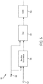
- FIG. 2 is a schematic diagram of an inverter circuit 200 with dynamic slew rate control, according to some embodiments.
- the inverter circuit 200 may include an external input terminal 212, an inverter 202, a driver 248, and a slew rate control module 244.
- the external input terminal 212 may receive a pulse width modulated (PWM) waveform 350 from, for example, a controller.
- the inverter 202 may include an input terminal 252 and an output terminal 250.
- the output terminal 250 may drive a load (not shown).
- the driver 248 may include a first input terminal 256, a second input terminal 258, and an output terminal 254.
- the first input terminal 256 of the driver 248 may be coupled to the external input terminal 212 of the inverter circuit 200.
- the output terminal 254 of the driver 248 may be coupled to the input terminal 252 of the inverter 202.
- the slew rate control module 244 may include a first input terminal 262, a second input terminal 264, and an output terminal 260.
- the first input terminal 262 of the slew rate control module 244 may be coupled to the external input terminal 212 of the inverter circuit 200.
- the second input terminal 246 of the slew rate control module 244 may receive a load current IL 246, which may indicate a magnitude of the load driven by the inverter circuit 200.
- a load current IL may be compared to one or more reference currents. Basing on the comparison results, the load driven by the inverter circuit may be determined as heavy, light, or middle-level.
- the output terminal 260 of the slew rate control module 244 may be coupled to the second input terminal 258 of the driver 248.
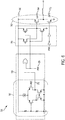
- FIG. 3 is a schematic diagram illustrating some implementation details of the inverter circuit 200, according to some embodiments.
- the inverter 202 may include a UGATE 204 and an LGATE 206.
- the UGATE 204 may be a p-type transistor;
- the LGATE 206 may be an n-type transistor.
- the driver 248 may include a transistor C, a transistor D, and a transistor E.
- the transistors C and E may be p-type transistors.
- the transistor D may be an n-type transistor.
- the transistors C and E may be connected in parallel.
- the transistor C may be connected to the transistor D in series.
- the slew rate control module 244 may include a comparator 266 and an OR gate 272.
- the comparator 266 may include an input terminal 264.
- the comparator 266 may compare a sense current Isense to a reference current IREF.
- the sense current Isense may correlate to the load current IL.
- the sense current Isense may indicate the magnitude of the load current IL.
- the output terminal 268 of the comparator 266 may be a low voltage when the sense current Isense is higher than the reference current IREF; the output terminal 268 of the comparator 266 may be a high voltage when Isense is lower than the reference current IREF.
- the OR gate 272 may include a first input terminal 270, a second input terminal 262, and an output terminal 260.
- the first input terminal 270 of the OR gate 272 may be coupled to the output terminal 268 of the comparator 266.
- the second input terminal 262 of the OR gate 272 may be coupled to the external input terminal 212 of the inverter circuit 200.
- the output terminal 260 of the OR gate 272 may be coupled to a gate terminal 258 of the transistor E.
- the above discussed circuit configuration modifies the slew rate of the driver 248 to a lower level when the inverter circuit 200 drives a heavy load.
- the inventors have recognized and appreciated that the slew rate of the driver 248 is controlled by the slower one of the output terminal 260 of the slew rate control module 244 and the external input terminal 212 of the inverter circuit 200.
- the UGATE 204 turns off when the output terminal 254 of the driver 248 goes high.
- the slew rate of the driver 248 at the output terminal 254 is controlled by both the output terminal 260 of the slew rate control module 244 and the external input terminal 212 of the inverter circuit 200.
- the falling edge transition of the PWM waveform 350 turns on the transistor C and off the transistor D.
- the output terminal 260 of the slew rate control module 244 going low turns on the transistor E.
- both the output terminal 270 of the comparator 266 and the PWM have to go low. Therefore, the output terminal 260 is controlled by the slower one of the comparator output and the PWM.
- a slew rate control module is illustrated with respect to the UGATE 204, a person of ordinary skill in the art would appreciate that the LGATE 206 may have a slew rate control module with respect to a rising edge transition of the PWM waveform 350.
- FIG. 4 is a flow chart illustrating a method 400 to dynamically control a slew rate of the driver 248, according to some embodiments.
- the method 400 may start form step 402 when an inverter circuit is instructed to operate with dynamic slew rate control by, for example, a system signal from a controller.
- a magnitude of a load current may be detected.
- the load current may be a current flowing through a load driven by the inverter circuit. 200.
- the magnitude of the load current may indicate the magnitude of the load driven by the inverter circuit.
- the magnitude of the detected load current may be evaluated by, for example, using the comparator 266.
- a slew rate of driver 248 may be modified to a first level (step 408), which may mean a slower falling/rising edge transition such that the problem of signal bounce may be mitigated.
- the slew rate of driver 248 may be modified to a second level that is higher than the first level (step 410), which may mean a faster falling/rising edge transition.
- FIG. 5 is a schematic diagram of an inverter circuit 500 with dynamic slew rate control, according to some embodiments.
- a slew rate control module 544 may receive an input voltage VIN 546, which may indicate a magnitude of a load driven by the inverter circuit 500.
- the input voltage may be compared to one or more reference voltages. Basing on the comparison results, the load driven by the inverter circuit may be determined as heavy, light, or middle-level.
- FIG. 6 is a schematic diagram illustrating some implementation details of the inverter circuit 500, according to some embodiments.
- the slew rate control module 544 compares the input voltage VIN to a reference voltage VREF.
- the output terminal 568 of a comparator 566 may be a low voltage when the input voltage VIN is higher than the reference voltage VREF; the output terminal 568 of the comparator 566 may be a high voltage when VIN is lower than the reference VREF.
- LGATE 506 may have a slew rate control module with respect to a rising edge transition of the PWM waveform 650.
- FIG. 7 is a flow chart illustrating a method 700 to dynamically control a slew rate of the inverter's driver 548, according to some embodiments.
- the method 700 may start form step 702 when an inverter circuit is instructed to operate with dynamic slew rate control by, for example, a system signal from a controller.
- a magnitude of an input voltage may be detected.
- the input voltage may be a voltage shared by a load driven by the inverter circuit 500.
- the magnitude of the input voltage may indicate the magnitude of the load driven by the inverter circuit.
- the magnitude of the detected input voltage may be evaluated by, for example, using the comparator 566.
- a slew rate of the driver 548 may be modified to a third level (step 708), which may mean a slower falling/rising edge transition such that the problem of signal bounce may be mitigated.
- the slew rate of the driver 548 may be modified to a fourth level that is higher than the third level (step 710), which may mean a faster falling/rising edge transition.
- FIG. 8 is a schematic diagram of an inverter circuit 800 with dynamic slew rate control, according to some embodiments.
- the slew rate control module 844 may also receive a signal 882 from a controller 880.
- the signal 882 may indicate a mode configuration of the inverter circuit 800.
- the mode configuration of the inverter circuit may be selected from a plurality of modes such as dynamic voltage scaling (DVS) mode and multi-phase mode.
- DVDS dynamic voltage scaling
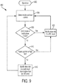
- FIG. 9 is a flow chart illustrating a method 900 to dynamically control slew rate of an inverter's driver 848 in FIG. 8 , according to some embodiments.
- the method 900 may start form step 902 when an inverter circuit is instructed to operate with dynamic slew rate control by, for example, a system signal from a controller.
- a mode configuration of the inverter circuit 800 may be detected.
- the mode configuration of the inverter circuit may be selected from a plurality of modes such as dynamic voltage scaling (DVS) mode and multi-phase mode.
- it may be determined whether the inverter circuit 800 operating in the dynamic voltage scaling (DVS) mode or the multi-phase mode.
- DVDS dynamic voltage scaling
- a slew rate of driver 848 may be modified to a fifth level (step 908), which may mean a slower falling/rising edge transition such that the problem of signal bounce may be mitigated.
- the method 900 may proceed to step 910.
- a magnitude of a load driven by the inverter circuit 800 may also be detected at step 904. In some embodiments, a magnitude of a load driven by the inverter circuit 800 may be detected at a later step, for example, after step 906. In some embodiments, the magnitude of the load driven by the inverter circuit may be indicated by a load current. In some embodiments, the magnitude of the load driven by the inverter circuit may be indicated by an input voltage. At step 910, the magnitude of the load driven by the inverter circuit may be evaluated.
- a slew rate of the driver 848 may be modified to the fifth level (step 908), which may mean a slower falling/rising edge transition such that the problem of signal bounce may be mitigated.
- the slew rate of the driver 848 may be modified to a sixth level that is higher than the fifth level (step 912), which may mean a faster falling/rising edge transition.
- FIG. 10A is a graph that compares safe operation areas (SOAs) under different loading conditions for transistors in an inverter's driver without dynamic slew rate control, such as the UGATE_DRIVER 108.
- a curve 1002A illustrates an intrinsic SOA of a transistor, for example, without the influence of any load.
- a curve 1004A indicates an SOA of the transistor under a heavy loading condition.
- a curve 1006A indicates an SOA of the transistor under a light loading condition. The SOA of the transistor is adversely reduced from the intrinsic SOA due to the loading conditions.
- the curve 1002A indicates that, without any load, the transistor will function normally as long as a drain terminal of the transistor is biased below 8 V (V_DS); the curve 1004A indicates that, with a heavy load, the drain terminal of the transistor should be biased below 6.4 V to ensure the transistor function normally; and the curve 1006A indicates that, with a light load, the drain terminal of the transistor should be biased below 6 V to ensure the transistor function normally.
- FIG. 10B is a graph that compares SOAs under different loading conditions for transistors in an inverter's driver with dynamic slew rate control, according to some embodiments.
- a curve 1002B illustrates an intrinsic SOA of a transistor, for example, without the influence of any load.
- a curve 1004B indicates an SOA of the transistor under a heavy loading condition.
- a curve 1006B indicates an SOA of the transistor under a light loading condition.
- curves 1004B and 1006B indicate an enlarged SOA for transistors in an inverter's driver with dynamic slew rate control compared with transistors in an inverter's driver without slew rate control.
- the curve 1002B indicates that, without any load, the transistor will function normally as long as a drain terminal of the transistor is biased below 8 V (V_DS); unlike the curve 1004A, the curve 1004B indicates that, with a heavy load, a safe operation range of the drain terminal of the transistor is extended to 7.2 V from 6.4 V; and unlike the curve 1006A, the curve 1006B indicates that, with a light load, a safe operation range of the drain terminal of the transistor is extended to 7.2 V from 6 V.
- the terms “approximately”, “substantially,” and “about” may be used to mean within ⁇ 20% of a target value in some embodiments, within ⁇ 10% of a target value in some embodiments, within ⁇ 5% of a target value in some embodiments, and yet within ⁇ 2% of a target value in some embodiments.
Landscapes
- Engineering & Computer Science (AREA)
- Power Engineering (AREA)
- Power Conversion In General (AREA)
Abstract
Description
- The present disclosure relates to inverter circuits, and in particular to inverter circuits with dynamic slew rate control.
- Inverter circuits are used for many applications including, for example, output bus drivers, switching regulators, and DC-to-DC converters. An inverter circuit may be joined with other circuits on a printed circuit board (PCB) to form an electronic assembly, which may be packaged alone or with other electronic assemblies.
- Inverter circuits with dynamic slew rate control are provided.
- Some embodiments relate to a method for controlling a driver of an inverter. The method may comprise detecting a magnitude of a load driven by the inverter, and modifying a slew rate of the driver of the inverter based on the magnitude of the load.
- In some embodiments, modifying the slew rate of the driver of the inverter may comprise reducing the slew rate of the driver of the inverter when the detected magnitude of the load increases.
- In some embodiments, modifying the slew rate of the driver of the inverter may comprise increasing the slew rate of the driver of the inverter when the detected magnitude of the load decreases.
- In some embodiments, the detecting step may comprise detecting a mode configuration of the inverter, and the modifying step may comprise modifying the slew rate of the driver of the inverter based on the detected mode configuration of the inverter.
- In some embodiments, the mode configuration of the inverter circuit may be selected from a plurality of modes comprising dynamic voltage scaling (DVS) mode and multi-phase mode.
- In some embodiments, detecting the magnitude of the load driven by the inverter may comprise detecting a current representing a load current.
- In some embodiments, modifying the slew rate of the driver of the inverter may comprise modifying the slew rate of the driver of the inverter to a first predetermined level when the detected current is higher than a reference current.
- In some embodiments, modifying the slew rate of the driver of the inverter may comprise modifying the slew rate of the driver of the inverter to a second predetermined level when the detected current is lower than the reference current, wherein the second predetermined level is higher than the first predetermined level.
- In some embodiments, detecting the magnitude of the load driven by the inverter may comprise detecting a voltage representing an input voltage.
- In some embodiments, modifying the slew rate of the driver of the inverter may comprise modifying the slew rate of the driver of the inverter to a third predetermined level when the detected voltage is higher than a reference voltage.
- In some embodiments, modifying the slew rate of the driver of the inverter may comprise modifying the slew rate of the driver of the inverter to a fourth predetermined level when the detected voltage is lower than the reference voltage, wherein the fourth predetermined level is higher than the third predetermined level.
- Some embodiments relate to an inverter circuit. The inverter circuit may include an inverter, a driver coupled to the inverter, the driver being configured to receive a first signal, and a slew rate control module coupled to the driver. The slew rate control module may be configured to receive the first signal and a second signal indicating a magnitude of a load driven by the inverter circuit. The slew rate control module may modify a slew rate of the driver based on the second signal.
- In some embodiments, the slew rate control module may be configured to receive a third signal indicating a mode configuration of the inverter circuit, and the slew rate control module may modify the slew rate of the driver based on the third signal.
- In some embodiments, the mode configuration of the inverter circuit may be selected from a plurality of modes comprising dynamic voltage scaling (DVS) mode and multi-phase mode.
- In some embodiments, the second signal may be a current representing a load current, and the slew rate control module may comprise a comparator configured to compare the current to a reference current.
- In some embodiments, the slew rate control module may comprise an OR gate configured to receive the first signal and an output of the comparator, and the OR gate may output to the driver.
- In some embodiments, the second signal may be a voltage representing an input voltage, and the slew rate control module may comprise a comparator configured to compare the voltage to a reference voltage.
- In some embodiments, the slew rate control module may comprise an OR gate configured to receive the first signal and an output of the comparator, and the OR gate may output to the driver.
- In some embodiments, the slew rate control module may reduce the slew rate of the driver when the second signal indicates that the magnitude of the load increases.
- In some embodiments, the slew rate control module may increase the slew rate of the driver when the second signal indicates that the magnitude of the load decreases.
- The foregoing summary is provided by way of illustration and is not intended to be limiting.
- In the drawings, each identical or nearly identical component that is illustrated in various figures is represented by a like numeral. For purposes of clarity, not every component may be labeled in every drawing. The accompanying drawings are not necessarily drawn to scale, with emphasis instead being placed on illustrating various aspects of the techniques and devices described herein.
-
FIG. 1A is a schematic diagram of an inverter circuit without dynamic slew rate control. -
FIG. 1B is a schematic timing diagram, illustrating signal bounce in the inverter circuit ofFIG. 1A . -
FIG. 2 is a schematic diagram of an inverter circuit with dynamic slew rate control by a current representing a load current, according to some embodiments. -
FIG. 3 is a schematic diagram illustrating some implementation details of the inverter circuit ofFIG. 2 , according to some embodiments. -
FIG. 4 is a flow chart illustrating an alternative method to dynamically control a slew rate of the inverter's driver inFIG. 2 , according to some embodiments. -
FIG. 5 is a schematic diagram of an inverter circuit with dynamic slew rate control by a voltage representing an input voltage, according to some embodiments. -
FIG. 6 is a schematic diagram illustrating some implementation details of the inverter circuit ofFIG. 5 , according to some embodiments. -
FIG. 7 is a flow chart illustrating a second alternative method to dynamically control a slew rate of the inverter's driver inFIG. 5 , according to some embodiments. -
FIG. 8 is a schematic diagram of an inverter circuit with dynamic slew rate control by a mode configuration of the inverter circuit, according to some embodiments. -
FIG. 9 is a flow chart illustrating a method to dynamically control a slew rate of the inverter's driver inFIG. 8 , according to some embodiments. -
FIG. 10A is a graph that compares safe operating areas (SOAs) under different loading conditions for transistors in an inverter's driver without dynamic slew rate control. -
FIG. 10B is a graph that compares SOAs under different loading conditions for transistors in an inverter's driver with dynamic slew rate control, according to some embodiments. - The inventors have recognized and appreciated that, for circuits with a wide dynamic current range, parasitic resistances and inductances introduced by a printed circuit board (PCB) or other packaging components may cause signal bounce, in which the signal varies in response to transients. Signal bounce includes, for example, ground bounce, supply voltage bounce, and output voltage bounce. As an example of ground bounce, a parasitic inductor may be connected between an internal device ground and an external system ground. A voltage across the parasitic inductor due to a varying current may cause the internal ground to be at a different potential than the external ground. Some devices in the circuit may be stressed and perhaps damaged due to the internal-to-external ground potential difference.
- The inventors have recognized and appreciated that conventional solutions keep the slew rate of an inverter's driver at the same level for various loading conditions and mode configurations. However, arbitrarily selecting one slew rate for various loading conditions and mode configurations may cause issues. For example, if the slew rate is selected under the heaviest loading condition, peak power efficiency of a converter circuit (e.g., a buck converter) may be poor, e.g., lower than 80%. On the other hand, if a slew rate is selected by Pulse Frequency Mode (PFM) peak current, it may be difficult to design package components (e.g., PCB layout), or Laterally Diffused MOSFET (LDMOS) may be needed. As a result, a safe operating area (SOA) of transistors in the inverter's driver is reduced (e.g.,
FIG. 10A ). An SOA may refer to the voltage and current conditions over which a transistor can be expected to operate normally. A transistor operating outside its SOA may cause a circuit malfunction. A person of ordinary skill in the art would recognize that the SOA may be presented in transistor datasheets as a graph with drain-to-source voltage (VDS) as x axis and gate-to-source voltage (VGS) as y axis; the SOA may refer to the area under the curve. However, the techniques described herein are not limited as to a particular manner of illustrating the SOA. - The inventors have recognized and appreciated that dynamically controlling slew rate of an inverter circuit may allow improved or maximized utilization of transistors' SOA. Signal bounce may be more serious when an inverter circuit drives a heavy load than when it drives a light or middle-level load. The currents and/or voltages may be higher when the inverter circuit drives a heavy load than a light or middle-level load. A load driven by an inverter circuit may be determined as heavy, middle-level, or light by comparing a magnitude of the load to one or more threshold values. When the inverter circuit drives a heavy load, reducing the slew rate of the inverter's driver may mitigate the effect of signal bounce and thus allow the transistors in the inverter circuit to operate safely with a wider range of VDS for a particular VGS. On the other hand, when the inverter circuit drives a light or middle-level load, the slew rate of the inverter's driver may be increased over that used when the inverter circuit drives a heavy load, such that the inverter can produce an output voltage that responds more quickly.
- In some embodiments, an inverter circuit may include an inverter driven by a driver. A slew rate of an output of the driver may be controlled by a slew rate control module. Both the driver and the slew rate control module may receive a first signal. In some embodiments, the first signal may be a pulse width modulated (PWM) signal. The slew rate control module may receive a second signal indicating a magnitude of a load driven by the inverter circuit. In some embodiments, the slew rate control module may reduce the slew rate of the output of the driver when the second signal indicates that the magnitude of the load increases. In some embodiments, the slew rate control module may increase the slew rate of the output of the driver when the second signal indicates that the magnitude of the load decreases.
- In some embodiments, the second signal that indicates the magnitude of the load driven by the inverter circuit may be a signal representing a load current. In some embodiments, the second signal that indicates the magnitude of the load driven by the inverter circuit may be a voltage representing an input voltage.
- In some embodiments, the slew rate control module may receive a third signal that indicates a mode configuration of the inverter circuit. The mode configuration may be selected from a plurality of modes including dynamic voltage scaling (DVS) mode and multi-phase mode. The slew rate control module may modify a slew rate of the inverter's driver based on the mode configuration of the inverter circuit. In some embodiments, the slew rate control module may reduce the slew rate of the inverter's driver when the third signal indicates that the inverter circuit is operating in DVS mode or multi-phase mode.
-
FIG. 1A is a schematic diagram of aninverter circuit 100 without dynamic slew rate control. Theinverter circuit 100 may include aninput terminal 112 to receive a pulse width modulated (PWM)waveform 150, aninverter 102 having afirst transistor UGATE 104 and asecond transistor LGATE 106, afirst driver UGATE_DRIVER 108 to drive the UGATE, asecond driver LGATE_DRIVER 110 to drive the LGATE, anoutput capacitor C o 132, anoutput terminal V o 116 to drive a load (not shown), and apower supply Vin 114, which may be shared with the load. Thepower supply 114 may include a positivesupply voltage VDD 134 and a negativesupply voltage VSS 136. Theinverter 102 may include an internal positive powersupply voltage PVDD 118, an internal negative powersupply voltage PVSS 120, and aninternal output LX 122. The first and second drivers UGATE_DRIVER 108 andLGATE_DRIVER 110 may share the internal positive and negative power supplies PVDD and PVSS with theinverter 102. - The
inverter circuit 100 may also include parasitic resistances and inductances induced by packaging components. For example, bonding wires may induce parasitic resistances andinductances 124; PCB wirings may induce parasitic resistance andinductance 126, andparasitic capacitance C IN 130. The parasitic resistances andinductances supply voltage PVDD 118 and the positivesupply voltage VDD 134. The parasitic resistances andinductances supply voltage PVSS 120 and the negativesupply voltage VSS 136. - The
output terminal V o 116 may switch from a high voltage to a low voltage, which may be referred to as a falling edge transition, or may switch from a low voltage to a high voltage, which may be referred to as a rising edge transition. During switching, theoutput capacitor C o 132 and theparasitic capacitance C IN 130 may charge or discharge, and may generate transient currents. The transient currents may be a function of Co, CIN, and voltage changes on Co and CIN over time t (ΔV/Δt). The transient currents flowing through the parasitic resistances andinductances supply voltage PVDD 118 may be at a different voltage from the positivesupply voltage VDD 134; the internal negativesupply voltage PVSS 120 may be at a different voltage from the negativesupply voltage VSS 136. -
FIG. 1B is a schematic timing diagram, illustrating signal bounce in theinverter circuit 100 during a falling edge transition of thePWM waveform 150. Acurve 138 illustrates the potential level of the internal positivesupply voltage PVDD 118 over time t, showing supply voltage bounce 144. Acurve 140 illustrates the potential level of the internal negativesupply voltage PVSS 120 over time t, showingground bounce 146. Acurve 142 illustrates the potential level of the internal output LX over time t. During the falling edge transition of thePWM waveform 150, the internal output LX follows the internal negativesupply voltage PVSS 120, showingground bounce 148. Therefore, the NMOS transistors, e.g., in the UGATE_DRIVER, are stressed due to ground bounce, e.g., 146 and 148. -
FIG. 2 is a schematic diagram of aninverter circuit 200 with dynamic slew rate control, according to some embodiments. Theinverter circuit 200 may include anexternal input terminal 212, aninverter 202, adriver 248, and a slewrate control module 244. In some embodiments, theexternal input terminal 212 may receive a pulse width modulated (PWM)waveform 350 from, for example, a controller. Theinverter 202 may include aninput terminal 252 and anoutput terminal 250. In some embodiments, theoutput terminal 250 may drive a load (not shown). Thedriver 248 may include afirst input terminal 256, asecond input terminal 258, and anoutput terminal 254. Thefirst input terminal 256 of thedriver 248 may be coupled to theexternal input terminal 212 of theinverter circuit 200. Theoutput terminal 254 of thedriver 248 may be coupled to theinput terminal 252 of theinverter 202. - The slew
rate control module 244 may include afirst input terminal 262, asecond input terminal 264, and anoutput terminal 260. Thefirst input terminal 262 of the slewrate control module 244 may be coupled to theexternal input terminal 212 of theinverter circuit 200. Thesecond input terminal 246 of the slewrate control module 244 may receive a loadcurrent IL 246, which may indicate a magnitude of the load driven by theinverter circuit 200. In some embodiments, a load current IL may be compared to one or more reference currents. Basing on the comparison results, the load driven by the inverter circuit may be determined as heavy, light, or middle-level. Theoutput terminal 260 of the slewrate control module 244 may be coupled to thesecond input terminal 258 of thedriver 248. -
FIG. 3 is a schematic diagram illustrating some implementation details of theinverter circuit 200, according to some embodiments. Theinverter 202 may include a UGATE 204 and anLGATE 206. In some embodiments, theUGATE 204 may be a p-type transistor; theLGATE 206 may be an n-type transistor. Thedriver 248 may include a transistor C, a transistor D, and a transistor E. The transistors C and E may be p-type transistors. The transistor D may be an n-type transistor. The transistors C and E may be connected in parallel. The transistor C may be connected to the transistor D in series. - The slew
rate control module 244 may include acomparator 266 and anOR gate 272. Thecomparator 266 may include aninput terminal 264. Thecomparator 266 may compare a sense current Isense to a reference current IREF. In some embodiments, the sense current Isense may correlate to the load current IL. For example, the sense current Isense may indicate the magnitude of the load current IL. In some embodiments, theoutput terminal 268 of thecomparator 266 may be a low voltage when the sense current Isense is higher than the reference current IREF; theoutput terminal 268 of thecomparator 266 may be a high voltage when Isense is lower than the reference current IREF. The ORgate 272 may include afirst input terminal 270, asecond input terminal 262, and anoutput terminal 260. Thefirst input terminal 270 of theOR gate 272 may be coupled to theoutput terminal 268 of thecomparator 266. Thesecond input terminal 262 of theOR gate 272 may be coupled to theexternal input terminal 212 of theinverter circuit 200. Theoutput terminal 260 of theOR gate 272 may be coupled to agate terminal 258 of the transistor E. - The above discussed circuit configuration modifies the slew rate of the
driver 248 to a lower level when theinverter circuit 200 drives a heavy load. The inventors have recognized and appreciated that the slew rate of thedriver 248 is controlled by the slower one of theoutput terminal 260 of the slewrate control module 244 and theexternal input terminal 212 of theinverter circuit 200. For example, during a falling edge transition of thePWM waveform 350, theUGATE 204 turns off when theoutput terminal 254 of thedriver 248 goes high. The slew rate of thedriver 248 at theoutput terminal 254 is controlled by both theoutput terminal 260 of the slewrate control module 244 and theexternal input terminal 212 of theinverter circuit 200. The falling edge transition of thePWM waveform 350 turns on the transistor C and off the transistor D. Theoutput terminal 260 of the slewrate control module 244 going low turns on the transistor E. To turn theoutput terminal 260 of theOR gate 272 low, both theoutput terminal 270 of thecomparator 266 and the PWM have to go low. Therefore, theoutput terminal 260 is controlled by the slower one of the comparator output and the PWM. Although a slew rate control module is illustrated with respect to theUGATE 204, a person of ordinary skill in the art would appreciate that theLGATE 206 may have a slew rate control module with respect to a rising edge transition of thePWM waveform 350. -
FIG. 4 is a flow chart illustrating amethod 400 to dynamically control a slew rate of thedriver 248, according to some embodiments. Themethod 400 may startform step 402 when an inverter circuit is instructed to operate with dynamic slew rate control by, for example, a system signal from a controller. Atstep 404, a magnitude of a load current may be detected. The load current may be a current flowing through a load driven by the inverter circuit. 200. The magnitude of the load current may indicate the magnitude of the load driven by the inverter circuit. Atstep 406, the magnitude of the detected load current may be evaluated by, for example, using thecomparator 266. In some embodiments, if the magnitude of the detected load current is determined as heavy, for example, higher than the reference current IREF, a slew rate ofdriver 248 may be modified to a first level (step 408), which may mean a slower falling/rising edge transition such that the problem of signal bounce may be mitigated. On the other hand, if the magnitude of the detected load current is determined as not heavy, for example, lower than the reference current IREF, the slew rate ofdriver 248 may be modified to a second level that is higher than the first level (step 410), which may mean a faster falling/rising edge transition. -
FIG. 5 is a schematic diagram of aninverter circuit 500 with dynamic slew rate control, according to some embodiments. Instead of receiving the load current IL as illustrated inFIG. 2 , a slewrate control module 544 may receive aninput voltage VIN 546, which may indicate a magnitude of a load driven by theinverter circuit 500. In some embodiments, the input voltage may be compared to one or more reference voltages. Basing on the comparison results, the load driven by the inverter circuit may be determined as heavy, light, or middle-level. -
FIG. 6 is a schematic diagram illustrating some implementation details of theinverter circuit 500, according to some embodiments. Instead of comparing the sense current Isense to the reference current IREF as illustrated inFIG. 3 , the slewrate control module 544 compares the input voltage VIN to a reference voltage VREF. In some embodiments, theoutput terminal 568 of acomparator 566 may be a low voltage when the input voltage VIN is higher than the reference voltage VREF; theoutput terminal 568 of thecomparator 566 may be a high voltage when VIN is lower than the reference VREF. Although a slew rate control module is illustrated with respect to theUGATE 504, a person of ordinary skill in the art would appreciate that the LGATE 506 may have a slew rate control module with respect to a rising edge transition of thePWM waveform 650. -
FIG. 7 is a flow chart illustrating amethod 700 to dynamically control a slew rate of the inverter'sdriver 548, according to some embodiments. Themethod 700 may startform step 702 when an inverter circuit is instructed to operate with dynamic slew rate control by, for example, a system signal from a controller. Atstep 704, a magnitude of an input voltage may be detected. The input voltage may be a voltage shared by a load driven by theinverter circuit 500. The magnitude of the input voltage may indicate the magnitude of the load driven by the inverter circuit. Atstep 706, the magnitude of the detected input voltage may be evaluated by, for example, using thecomparator 566. In some embodiments, if the magnitude of the detected input voltage is determined as high, for example, higher than the reference voltage VREF, a slew rate of thedriver 548 may be modified to a third level (step 708), which may mean a slower falling/rising edge transition such that the problem of signal bounce may be mitigated. On the other hand, if the magnitude of the detected input voltage is determined as not high, for example, lower than the reference voltage VREF, the slew rate of thedriver 548 may be modified to a fourth level that is higher than the third level (step 710), which may mean a faster falling/rising edge transition. -
FIG. 8 is a schematic diagram of aninverter circuit 800 with dynamic slew rate control, according to some embodiments. In addition to receiving the load current IL as illustrated inFIG. 2 or the input voltage VIN as illustrated inFIG. 5 , the slewrate control module 844 may also receive asignal 882 from acontroller 880. Thesignal 882 may indicate a mode configuration of theinverter circuit 800. The mode configuration of the inverter circuit may be selected from a plurality of modes such as dynamic voltage scaling (DVS) mode and multi-phase mode. -
FIG. 9 is a flow chart illustrating amethod 900 to dynamically control slew rate of an inverter'sdriver 848 inFIG. 8 , according to some embodiments. Themethod 900 may startform step 902 when an inverter circuit is instructed to operate with dynamic slew rate control by, for example, a system signal from a controller. Atstep 904, a mode configuration of theinverter circuit 800 may be detected. The mode configuration of the inverter circuit may be selected from a plurality of modes such as dynamic voltage scaling (DVS) mode and multi-phase mode. Atstep 906, it may be determined whether theinverter circuit 800 operating in the dynamic voltage scaling (DVS) mode or the multi-phase mode. In some embodiments, if it is determined that theinverter circuit 800 operates in either the dynamic voltage scaling (DVS) mode or the multi-phase mode, a slew rate ofdriver 848 may be modified to a fifth level (step 908), which may mean a slower falling/rising edge transition such that the problem of signal bounce may be mitigated. On the other hand, if it is determined that theinverter circuit 800 operates in neither the dynamic voltage scaling (DVS) mode nor the multi-phase mode, themethod 900 may proceed to step 910. - In some embodiments, a magnitude of a load driven by the
inverter circuit 800 may also be detected atstep 904. In some embodiments, a magnitude of a load driven by theinverter circuit 800 may be detected at a later step, for example, afterstep 906. In some embodiments, the magnitude of the load driven by the inverter circuit may be indicated by a load current. In some embodiments, the magnitude of the load driven by the inverter circuit may be indicated by an input voltage. Atstep 910, the magnitude of the load driven by the inverter circuit may be evaluated. In some embodiments, if the magnitude of the load driven by the inverter circuit is determined as heavy, a slew rate of thedriver 848 may be modified to the fifth level (step 908), which may mean a slower falling/rising edge transition such that the problem of signal bounce may be mitigated. On the other hand, if the magnitude of the load driven by the inverter circuit is determined as not heavy, the slew rate of thedriver 848 may be modified to a sixth level that is higher than the fifth level (step 912), which may mean a faster falling/rising edge transition. -
FIG. 10A is a graph that compares safe operation areas (SOAs) under different loading conditions for transistors in an inverter's driver without dynamic slew rate control, such as theUGATE_DRIVER 108. A curve 1002A illustrates an intrinsic SOA of a transistor, for example, without the influence of any load. Acurve 1004A indicates an SOA of the transistor under a heavy loading condition. Acurve 1006A indicates an SOA of the transistor under a light loading condition. The SOA of the transistor is adversely reduced from the intrinsic SOA due to the loading conditions. For example, when a gate terminal of a transistor is biased at 2 V (V_GS), the curve 1002A indicates that, without any load, the transistor will function normally as long as a drain terminal of the transistor is biased below 8 V (V_DS); thecurve 1004A indicates that, with a heavy load, the drain terminal of the transistor should be biased below 6.4 V to ensure the transistor function normally; and thecurve 1006A indicates that, with a light load, the drain terminal of the transistor should be biased below 6 V to ensure the transistor function normally. -
FIG. 10B is a graph that compares SOAs under different loading conditions for transistors in an inverter's driver with dynamic slew rate control, according to some embodiments. Acurve 1002B illustrates an intrinsic SOA of a transistor, for example, without the influence of any load. Acurve 1004B indicates an SOA of the transistor under a heavy loading condition. Acurve 1006B indicates an SOA of the transistor under a light loading condition. While the SOA of the transistor is still adversely reduced from the intrinsic SOA due to the loading conditions, as highlighted bycircle 10B, curves 1004B and 1006B indicate an enlarged SOA for transistors in an inverter's driver with dynamic slew rate control compared with transistors in an inverter's driver without slew rate control. For example, when a gate terminal of a transistor is biased at 2 V (V_GS), like the curve 1002A, thecurve 1002B indicates that, without any load, the transistor will function normally as long as a drain terminal of the transistor is biased below 8 V (V_DS); unlike thecurve 1004A, thecurve 1004B indicates that, with a heavy load, a safe operation range of the drain terminal of the transistor is extended to 7.2 V from 6.4 V; and unlike thecurve 1006A, thecurve 1006B indicates that, with a light load, a safe operation range of the drain terminal of the transistor is extended to 7.2 V from 6 V. - Various aspects of the apparatus and techniques described herein may be used alone, in combination, or in a variety of arrangements not specially discussed in the embodiments described in the foregoing description and is therefore not limited in its application to the details and arrangement of components set forth in the foregoing description or illustrated in the drawings. For example, aspects described in one embodiment may be combined in any manner with aspects described in other embodiments.
- The terms "approximately", "substantially," and "about" may be used to mean within ±20% of a target value in some embodiments, within ±10% of a target value in some embodiments, within ±5% of a target value in some embodiments, and yet within ±2% of a target value in some embodiments.
- Use of ordinal terms such as "first," "second," "third," etc., in the claims to modify a claim element does not by itself connote any priority, precedence, or order of one claim element over another or the temporal order in which acts of a method are performed, but are used merely as labels to distinguish one claim element having a certain name from another element having a same name (but for use of the ordinal term) to distinguish the claim elements.
- Also, the phraseology and terminology used herein is for the purpose of description and should not be regarded as limiting. The use of "including," "comprising," or "having," "containing," "involving," and variations thereof herein, is meant to encompass the items listed thereafter and equivalents thereof as well as additional items.
Claims (15)
- An inverter circuit comprising:an inverter (202, 502, 802);a driver (248, 548, 848) coupled to the inverter, the driver being configured to receive a first signal (350, 650); anda slew rate control module (244, 544, 844) coupled to the driver, the slew rate control module being configured to receive the first signal and a second signal (246, 546) indicating a magnitude of a load driven by the inverter circuit, wherein the slew rate control module modifies a slew rate of the driver based on the second signal.
- The inverter circuit of claim 1, wherein the slew rate control module is configured to receive a third signal (882) indicating a mode configuration of the inverter circuit, and the slew rate control module modifies the slew rate of the driver based on the third signal.
- The inverter circuit of claim 2, wherein the mode configuration of the inverter circuit is selected from a plurality of modes comprising dynamic voltage scaling (DVS) mode and multi-phase mode.
- The inverter circuit of any proceeding claim, wherein the second signal is a current representing a load current, and the slew rate control module comprises a comparator (266) configured to compare the current to a reference current.
- The inverter circuit of claim 4, wherein the slew rate control module comprises an OR gate (272) configured to receive the first signal and an output of the comparator, and the OR gate outputs to the driver.
- The inverter circuit of any proceeding claim, wherein the second signal is a voltage representing an input voltage, and the slew rate control module comprises a comparator (566) configured to compare the voltage to a reference voltage.
- The inverter circuit of claim 6, wherein the slew rate control module comprises an OR gate configured to receive the first signal and an output of the comparator, and the OR gate outputs to the driver.
- The inverter circuit of any proceeding claim, wherein the slew rate control module reduces the slew rate of the driver when the second signal indicates that the magnitude of the load increases.
- The inverter circuit of any proceeding claim, wherein the slew rate control module increases the slew rate of the driver when the second signal indicates that the magnitude of the load decreases.
- The inverter circuit of claim 4, wherein the slew rate control module modifies the slew rate of the driver to a first predetermined level when the load current is higher than the reference current.
- The inverter circuit of claim 10, wherein the slew rate control module modifies the slew rate of the driver to a second predetermined level when the load current is lower than the reference current, wherein the second predetermined level is higher than the first predetermined level.
- The inverter circuit of claim 6, wherein the slew rate control module modifies the slew rate of the driver to a third predetermined level when the input voltage is higher than the reference voltage.
- The inverter circuit of claim 12, wherein the slew rate control module modifies the slew rate of to a fourth predetermined level when the input voltage is lower than the reference voltage, wherein the fourth predetermined level is higher than the third predetermined level.
- The inverter circuit of any of claim 2 or claim 3, wherein the slew rate control module modifies the slew rate of the driver to a fifth predetermined level when the third signal indicates the inverter circuit operates in dynamic voltage scaling (DVS) mode or multi-phase mode, wherein the slew rate control module modifies the slew rate of the driver to a sixth predetermined level when the third signal indicates that the inverter circuit operates in neither DVS mode or multi-phase mode, and the second signal indicates that the magnitude of the load is lower than a threshold value, and wherein the sixth predetermined level is higher than the fifth predetermined level.
- A method for controlling a driver of an inverter, the method comprising:detecting a magnitude of a load driven by the inverter; andmodifying a slew rate of the driver of the inverter based on the magnitude of the load.
Applications Claiming Priority (2)
| Application Number | Priority Date | Filing Date | Title |
|---|---|---|---|
| US201762467864P | 2017-03-07 | 2017-03-07 | |
| US15/912,396 US10784763B2 (en) | 2017-03-07 | 2018-03-05 | Dynamic slew rate control |
Publications (2)
| Publication Number | Publication Date |
|---|---|
| EP3373434A1 true EP3373434A1 (en) | 2018-09-12 |
| EP3373434B1 EP3373434B1 (en) | 2021-07-07 |
Family
ID=61616806
Family Applications (1)
| Application Number | Title | Priority Date | Filing Date |
|---|---|---|---|
| EP18160591.6A Active EP3373434B1 (en) | 2017-03-07 | 2018-03-07 | Dynamic slew rate control |
Country Status (2)
| Country | Link |
|---|---|
| US (1) | US10784763B2 (en) |
| EP (1) | EP3373434B1 (en) |
Cited By (1)
| Publication number | Priority date | Publication date | Assignee | Title |
|---|---|---|---|---|
| WO2024048884A1 (en) | 2022-09-02 | 2024-03-07 | Lg Electronics Inc. | Power supply device and operating method thereof |
Families Citing this family (3)
| Publication number | Priority date | Publication date | Assignee | Title |
|---|---|---|---|---|
| DE102019102929B3 (en) * | 2019-02-06 | 2020-07-09 | Infineon Technologies Ag | Intelligent semiconductor switch |
| US11522439B2 (en) | 2020-01-16 | 2022-12-06 | Mediatek Inc. | Switching regulator with driver power clamp |
| US11804783B2 (en) | 2022-02-01 | 2023-10-31 | Silanna Asia Pte Ltd | Dynamic intra-pulse-sequence switch transition-time controller |
Citations (3)
| Publication number | Priority date | Publication date | Assignee | Title |
|---|---|---|---|---|
| US20120062190A1 (en) * | 2010-09-10 | 2012-03-15 | Holger Haiplik | Dc-dc converters |
| US20140159687A1 (en) * | 2012-12-07 | 2014-06-12 | Samsung Electronics Co., Ltd. | Adaptive Power Converters and Methods of Operating the Same |
| US20140232362A1 (en) * | 2013-02-21 | 2014-08-21 | Qualcomm Incorporated | Method and apparatus for improving device reliability using estimated current in a dynamic programmable switcher driver |
Family Cites Families (15)
| Publication number | Priority date | Publication date | Assignee | Title |
|---|---|---|---|---|
| US5408150A (en) | 1992-06-04 | 1995-04-18 | Linear Technology Corporation | Circuit for driving two power mosfets in a half-bridge configuration |
| US5481178A (en) | 1993-03-23 | 1996-01-02 | Linear Technology Corporation | Control circuit and method for maintaining high efficiency over broad current ranges in a switching regulator circuit |
| US5705919A (en) | 1996-09-30 | 1998-01-06 | Linear Technology Corporation | Low drop-out switching regulator architecture |
| US5929620A (en) | 1996-11-07 | 1999-07-27 | Linear Technology Corporation | Switching regulators having a synchronizable oscillator frequency with constant ramp amplitude |
| US6144194A (en) | 1998-07-13 | 2000-11-07 | Linear Technology Corp. | Polyphase synchronous switching voltage regulators |
| US6177787B1 (en) | 1998-09-11 | 2001-01-23 | Linear Technology Corporation | Circuits and methods for controlling timing and slope compensation in switching regulators |
| US6100678A (en) | 1999-08-26 | 2000-08-08 | Linear Technology Corporation | Single package pin providing soft-start and short-circuit timer functions in a voltage regulator controller |
| US6803752B1 (en) | 2000-02-14 | 2004-10-12 | Linear Technology Corporation | Polyphase PWM regulator with high efficiency at light loads |
| US6441653B1 (en) | 2001-02-20 | 2002-08-27 | Texas Instruments Incorporated | CMOS output driver with slew rate control |
| DE102007028568B4 (en) | 2006-06-23 | 2009-12-03 | Mediatek Inc. | switching regulators |
| US7768228B2 (en) | 2007-09-12 | 2010-08-03 | Gm Global Technology Operations, Inc. | Method and system for converting DC power to AC power |
| US8760136B2 (en) * | 2010-03-08 | 2014-06-24 | Freescale Semiconductor, Inc. | Dynamic voltage scaling interface |
| WO2015106686A1 (en) | 2014-01-14 | 2015-07-23 | Mediatek Inc. | Voltage supply circuits and controlling methods therefor |
| CN105634310B (en) | 2014-11-06 | 2018-09-04 | 台达电子工业股份有限公司 | Control signal generating system, inverter control device and related control circuit thereof |
| US9954440B2 (en) | 2016-05-13 | 2018-04-24 | Mediatek Inc. | Controller for DC/DC power converters |
-
2018
- 2018-03-05 US US15/912,396 patent/US10784763B2/en active Active
- 2018-03-07 EP EP18160591.6A patent/EP3373434B1/en active Active
Patent Citations (3)
| Publication number | Priority date | Publication date | Assignee | Title |
|---|---|---|---|---|
| US20120062190A1 (en) * | 2010-09-10 | 2012-03-15 | Holger Haiplik | Dc-dc converters |
| US20140159687A1 (en) * | 2012-12-07 | 2014-06-12 | Samsung Electronics Co., Ltd. | Adaptive Power Converters and Methods of Operating the Same |
| US20140232362A1 (en) * | 2013-02-21 | 2014-08-21 | Qualcomm Incorporated | Method and apparatus for improving device reliability using estimated current in a dynamic programmable switcher driver |
Cited By (2)
| Publication number | Priority date | Publication date | Assignee | Title |
|---|---|---|---|---|
| WO2024048884A1 (en) | 2022-09-02 | 2024-03-07 | Lg Electronics Inc. | Power supply device and operating method thereof |
| EP4581736A4 (en) * | 2022-09-02 | 2025-12-17 | Lg Electronics Inc | POWER SUPPLY DEVICE AND OPERATING PROCEDURES FOR IT |
Also Published As
| Publication number | Publication date |
|---|---|
| EP3373434B1 (en) | 2021-07-07 |
| US20180262097A1 (en) | 2018-09-13 |
| US10784763B2 (en) | 2020-09-22 |
Similar Documents
| Publication | Publication Date | Title |
|---|---|---|
| US9917584B2 (en) | Voltage converter integrated circuit with an integrated bootstrap capacitor | |
| CN104467369B (en) | System and Method for a Switch Driver | |
| US8018255B2 (en) | DC-DC converter, driver IC, and system in package | |
| US20110043955A1 (en) | Electrostatic discharge protection circuit, control method therefor, and switching regulator using same | |
| US8497714B2 (en) | System and method for driving a switch transistor | |
| US9859883B2 (en) | Gate driver and control method thereof | |
| US20150091539A1 (en) | Half-bridge gate driver control | |
| US9685865B2 (en) | Power-supply apparatus having a high-side transistor and a low-side transistor | |
| US20080084197A1 (en) | Low-noise DC/DC convertor with controlled diode conduction | |
| US11387734B2 (en) | Power converter architecture using lower voltage power devices | |
| EP3373434B1 (en) | Dynamic slew rate control | |
| CN105391298A (en) | Switching Converter Control | |
| US20120044723A1 (en) | Systems and methods for reducing standby power consumption of switch-mode power converters | |
| US10075079B2 (en) | Driver for low emission switching regulator | |
| US20140062431A1 (en) | Dc-dc converter and semiconductor device | |
| US10447138B2 (en) | Converter configured to convert a DC input voltage to a DC output voltage and including at least one resistive element | |
| US20260018997A1 (en) | Power supply control device | |
| US9866099B1 (en) | Adaptive high-side gate drive for ringing mitigation in switching power converters | |
| US11641162B2 (en) | Circuits and methods for generating a supply voltage for a switching regulator | |
| JP7568502B2 (en) | Switching power supply circuit and switching power supply device | |
| TWI678064B (en) | Inverter circuit and method for controlling driver of inverter circuit | |
| US7994759B2 (en) | System and method for driving a power supply device in an initial activation stage | |
| US11081955B2 (en) | Unidirectional ring mitigation in a voltage converter | |
| US10008930B1 (en) | Bootstrap circuit and associated direct current-to-direct current converter applying the bootstrap circuit | |
| US12051963B2 (en) | Minimum peak current for power converter |
Legal Events
| Date | Code | Title | Description |
|---|---|---|---|
| PUAI | Public reference made under article 153(3) epc to a published international application that has entered the european phase |
Free format text: ORIGINAL CODE: 0009012 |
|
| STAA | Information on the status of an ep patent application or granted ep patent |
Free format text: STATUS: THE APPLICATION HAS BEEN PUBLISHED |
|
| AK | Designated contracting states |
Kind code of ref document: A1 Designated state(s): AL AT BE BG CH CY CZ DE DK EE ES FI FR GB GR HR HU IE IS IT LI LT LU LV MC MK MT NL NO PL PT RO RS SE SI SK SM TR |
|
| AX | Request for extension of the european patent |
Extension state: BA ME |
|
| STAA | Information on the status of an ep patent application or granted ep patent |
Free format text: STATUS: REQUEST FOR EXAMINATION WAS MADE |
|
| 17P | Request for examination filed |
Effective date: 20190225 |
|
| RBV | Designated contracting states (corrected) |
Designated state(s): AL AT BE BG CH CY CZ DE DK EE ES FI FR GB GR HR HU IE IS IT LI LT LU LV MC MK MT NL NO PL PT RO RS SE SI SK SM TR |
|
| STAA | Information on the status of an ep patent application or granted ep patent |
Free format text: STATUS: EXAMINATION IS IN PROGRESS |
|
| 17Q | First examination report despatched |
Effective date: 20200624 |
|
| GRAP | Despatch of communication of intention to grant a patent |
Free format text: ORIGINAL CODE: EPIDOSNIGR1 |
|
| STAA | Information on the status of an ep patent application or granted ep patent |
Free format text: STATUS: GRANT OF PATENT IS INTENDED |
|
| INTG | Intention to grant announced |
Effective date: 20210127 |
|
| RAP1 | Party data changed (applicant data changed or rights of an application transferred) |
Owner name: MEDIATEK INC. |
|
| RIN1 | Information on inventor provided before grant (corrected) |
Inventor name: CHU, KUAN-YU Inventor name: HONG, SHAN-FONG Inventor name: LI, CHIH-CHEN Inventor name: HUANG, HUACHIANG |
|
| GRAS | Grant fee paid |
Free format text: ORIGINAL CODE: EPIDOSNIGR3 |
|
| GRAA | (expected) grant |
Free format text: ORIGINAL CODE: 0009210 |
|
| STAA | Information on the status of an ep patent application or granted ep patent |
Free format text: STATUS: THE PATENT HAS BEEN GRANTED |
|
| AK | Designated contracting states |
Kind code of ref document: B1 Designated state(s): AL AT BE BG CH CY CZ DE DK EE ES FI FR GB GR HR HU IE IS IT LI LT LU LV MC MK MT NL NO PL PT RO RS SE SI SK SM TR |
|
| REG | Reference to a national code |
Ref country code: GB Ref legal event code: FG4D |
|
| REG | Reference to a national code |
Ref country code: AT Ref legal event code: REF Ref document number: 1409540 Country of ref document: AT Kind code of ref document: T Effective date: 20210715 |
|
| REG | Reference to a national code |
Ref country code: DE Ref legal event code: R096 Ref document number: 602018019545 Country of ref document: DE |
|
| REG | Reference to a national code |
Ref country code: IE Ref legal event code: FG4D |
|
| REG | Reference to a national code |
Ref country code: LT Ref legal event code: MG9D |
|
| REG | Reference to a national code |
Ref country code: NL Ref legal event code: MP Effective date: 20210707 |
|
| REG | Reference to a national code |
Ref country code: AT Ref legal event code: MK05 Ref document number: 1409540 Country of ref document: AT Kind code of ref document: T Effective date: 20210707 |
|
| PG25 | Lapsed in a contracting state [announced via postgrant information from national office to epo] |
Ref country code: RS Free format text: LAPSE BECAUSE OF FAILURE TO SUBMIT A TRANSLATION OF THE DESCRIPTION OR TO PAY THE FEE WITHIN THE PRESCRIBED TIME-LIMIT Effective date: 20210707 Ref country code: SE Free format text: LAPSE BECAUSE OF FAILURE TO SUBMIT A TRANSLATION OF THE DESCRIPTION OR TO PAY THE FEE WITHIN THE PRESCRIBED TIME-LIMIT Effective date: 20210707 Ref country code: HR Free format text: LAPSE BECAUSE OF FAILURE TO SUBMIT A TRANSLATION OF THE DESCRIPTION OR TO PAY THE FEE WITHIN THE PRESCRIBED TIME-LIMIT Effective date: 20210707 Ref country code: FI Free format text: LAPSE BECAUSE OF FAILURE TO SUBMIT A TRANSLATION OF THE DESCRIPTION OR TO PAY THE FEE WITHIN THE PRESCRIBED TIME-LIMIT Effective date: 20210707 Ref country code: ES Free format text: LAPSE BECAUSE OF FAILURE TO SUBMIT A TRANSLATION OF THE DESCRIPTION OR TO PAY THE FEE WITHIN THE PRESCRIBED TIME-LIMIT Effective date: 20210707 Ref country code: LT Free format text: LAPSE BECAUSE OF FAILURE TO SUBMIT A TRANSLATION OF THE DESCRIPTION OR TO PAY THE FEE WITHIN THE PRESCRIBED TIME-LIMIT Effective date: 20210707 Ref country code: BG Free format text: LAPSE BECAUSE OF FAILURE TO SUBMIT A TRANSLATION OF THE DESCRIPTION OR TO PAY THE FEE WITHIN THE PRESCRIBED TIME-LIMIT Effective date: 20211007 Ref country code: AT Free format text: LAPSE BECAUSE OF FAILURE TO SUBMIT A TRANSLATION OF THE DESCRIPTION OR TO PAY THE FEE WITHIN THE PRESCRIBED TIME-LIMIT Effective date: 20210707 Ref country code: PT Free format text: LAPSE BECAUSE OF FAILURE TO SUBMIT A TRANSLATION OF THE DESCRIPTION OR TO PAY THE FEE WITHIN THE PRESCRIBED TIME-LIMIT Effective date: 20211108 Ref country code: NO Free format text: LAPSE BECAUSE OF FAILURE TO SUBMIT A TRANSLATION OF THE DESCRIPTION OR TO PAY THE FEE WITHIN THE PRESCRIBED TIME-LIMIT Effective date: 20211007 Ref country code: NL Free format text: LAPSE BECAUSE OF FAILURE TO SUBMIT A TRANSLATION OF THE DESCRIPTION OR TO PAY THE FEE WITHIN THE PRESCRIBED TIME-LIMIT Effective date: 20210707 |
|
| PG25 | Lapsed in a contracting state [announced via postgrant information from national office to epo] |
Ref country code: PL Free format text: LAPSE BECAUSE OF FAILURE TO SUBMIT A TRANSLATION OF THE DESCRIPTION OR TO PAY THE FEE WITHIN THE PRESCRIBED TIME-LIMIT Effective date: 20210707 Ref country code: LV Free format text: LAPSE BECAUSE OF FAILURE TO SUBMIT A TRANSLATION OF THE DESCRIPTION OR TO PAY THE FEE WITHIN THE PRESCRIBED TIME-LIMIT Effective date: 20210707 Ref country code: GR Free format text: LAPSE BECAUSE OF FAILURE TO SUBMIT A TRANSLATION OF THE DESCRIPTION OR TO PAY THE FEE WITHIN THE PRESCRIBED TIME-LIMIT Effective date: 20211008 |
|
| REG | Reference to a national code |
Ref country code: DE Ref legal event code: R097 Ref document number: 602018019545 Country of ref document: DE |
|
| PG25 | Lapsed in a contracting state [announced via postgrant information from national office to epo] |
Ref country code: DK Free format text: LAPSE BECAUSE OF FAILURE TO SUBMIT A TRANSLATION OF THE DESCRIPTION OR TO PAY THE FEE WITHIN THE PRESCRIBED TIME-LIMIT Effective date: 20210707 |
|
| PLBE | No opposition filed within time limit |
Free format text: ORIGINAL CODE: 0009261 |
|
| STAA | Information on the status of an ep patent application or granted ep patent |
Free format text: STATUS: NO OPPOSITION FILED WITHIN TIME LIMIT |
|
| PG25 | Lapsed in a contracting state [announced via postgrant information from national office to epo] |
Ref country code: SM Free format text: LAPSE BECAUSE OF FAILURE TO SUBMIT A TRANSLATION OF THE DESCRIPTION OR TO PAY THE FEE WITHIN THE PRESCRIBED TIME-LIMIT Effective date: 20210707 Ref country code: SK Free format text: LAPSE BECAUSE OF FAILURE TO SUBMIT A TRANSLATION OF THE DESCRIPTION OR TO PAY THE FEE WITHIN THE PRESCRIBED TIME-LIMIT Effective date: 20210707 Ref country code: RO Free format text: LAPSE BECAUSE OF FAILURE TO SUBMIT A TRANSLATION OF THE DESCRIPTION OR TO PAY THE FEE WITHIN THE PRESCRIBED TIME-LIMIT Effective date: 20210707 Ref country code: EE Free format text: LAPSE BECAUSE OF FAILURE TO SUBMIT A TRANSLATION OF THE DESCRIPTION OR TO PAY THE FEE WITHIN THE PRESCRIBED TIME-LIMIT Effective date: 20210707 Ref country code: CZ Free format text: LAPSE BECAUSE OF FAILURE TO SUBMIT A TRANSLATION OF THE DESCRIPTION OR TO PAY THE FEE WITHIN THE PRESCRIBED TIME-LIMIT Effective date: 20210707 Ref country code: AL Free format text: LAPSE BECAUSE OF FAILURE TO SUBMIT A TRANSLATION OF THE DESCRIPTION OR TO PAY THE FEE WITHIN THE PRESCRIBED TIME-LIMIT Effective date: 20210707 |
|
| 26N | No opposition filed |
Effective date: 20220408 |
|
| PG25 | Lapsed in a contracting state [announced via postgrant information from national office to epo] |
Ref country code: IT Free format text: LAPSE BECAUSE OF FAILURE TO SUBMIT A TRANSLATION OF THE DESCRIPTION OR TO PAY THE FEE WITHIN THE PRESCRIBED TIME-LIMIT Effective date: 20210707 |
|
| PG25 | Lapsed in a contracting state [announced via postgrant information from national office to epo] |
Ref country code: MC Free format text: LAPSE BECAUSE OF FAILURE TO SUBMIT A TRANSLATION OF THE DESCRIPTION OR TO PAY THE FEE WITHIN THE PRESCRIBED TIME-LIMIT Effective date: 20210707 |
|
| REG | Reference to a national code |
Ref country code: CH Ref legal event code: PL |
|
| REG | Reference to a national code |
Ref country code: BE Ref legal event code: MM Effective date: 20220331 |
|
| PG25 | Lapsed in a contracting state [announced via postgrant information from national office to epo] |
Ref country code: LU Free format text: LAPSE BECAUSE OF NON-PAYMENT OF DUE FEES Effective date: 20220307 Ref country code: LI Free format text: LAPSE BECAUSE OF NON-PAYMENT OF DUE FEES Effective date: 20220331 Ref country code: IE Free format text: LAPSE BECAUSE OF NON-PAYMENT OF DUE FEES Effective date: 20220307 Ref country code: CH Free format text: LAPSE BECAUSE OF NON-PAYMENT OF DUE FEES Effective date: 20220331 |
|
| PG25 | Lapsed in a contracting state [announced via postgrant information from national office to epo] |
Ref country code: BE Free format text: LAPSE BECAUSE OF NON-PAYMENT OF DUE FEES Effective date: 20220331 |
|
| P01 | Opt-out of the competence of the unified patent court (upc) registered |
Effective date: 20230607 |
|
| PG25 | Lapsed in a contracting state [announced via postgrant information from national office to epo] |
Ref country code: HU Free format text: LAPSE BECAUSE OF FAILURE TO SUBMIT A TRANSLATION OF THE DESCRIPTION OR TO PAY THE FEE WITHIN THE PRESCRIBED TIME-LIMIT; INVALID AB INITIO Effective date: 20180307 |
|
| PG25 | Lapsed in a contracting state [announced via postgrant information from national office to epo] |
Ref country code: MK Free format text: LAPSE BECAUSE OF FAILURE TO SUBMIT A TRANSLATION OF THE DESCRIPTION OR TO PAY THE FEE WITHIN THE PRESCRIBED TIME-LIMIT Effective date: 20210707 Ref country code: CY Free format text: LAPSE BECAUSE OF FAILURE TO SUBMIT A TRANSLATION OF THE DESCRIPTION OR TO PAY THE FEE WITHIN THE PRESCRIBED TIME-LIMIT Effective date: 20210707 |
|
| PG25 | Lapsed in a contracting state [announced via postgrant information from national office to epo] |
Ref country code: TR Free format text: LAPSE BECAUSE OF FAILURE TO SUBMIT A TRANSLATION OF THE DESCRIPTION OR TO PAY THE FEE WITHIN THE PRESCRIBED TIME-LIMIT Effective date: 20210707 |
|
| PG25 | Lapsed in a contracting state [announced via postgrant information from national office to epo] |
Ref country code: MT Free format text: LAPSE BECAUSE OF FAILURE TO SUBMIT A TRANSLATION OF THE DESCRIPTION OR TO PAY THE FEE WITHIN THE PRESCRIBED TIME-LIMIT Effective date: 20210707 |
|
| PGFP | Annual fee paid to national office [announced via postgrant information from national office to epo] |
Ref country code: FR Payment date: 20251231 Year of fee payment: 9 |
|
| PGFP | Annual fee paid to national office [announced via postgrant information from national office to epo] |
Ref country code: GB Payment date: 20260106 Year of fee payment: 9 |
|
| PGFP | Annual fee paid to national office [announced via postgrant information from national office to epo] |
Ref country code: DE Payment date: 20260102 Year of fee payment: 9 |