EP3373183A1 - System with soc connections among ip and multiple gpios, and corresponding method - Google Patents
System with soc connections among ip and multiple gpios, and corresponding method Download PDFInfo
- Publication number
- EP3373183A1 EP3373183A1 EP17305250.7A EP17305250A EP3373183A1 EP 3373183 A1 EP3373183 A1 EP 3373183A1 EP 17305250 A EP17305250 A EP 17305250A EP 3373183 A1 EP3373183 A1 EP 3373183A1
- Authority
- EP
- European Patent Office
- Prior art keywords
- gpio
- secure
- ipx
- ipy
- sportz
- Prior art date
- Legal status (The legal status is an assumption and is not a legal conclusion. Google has not performed a legal analysis and makes no representation as to the accuracy of the status listed.)
- Granted
Links
Images




Classifications
-
- G—PHYSICS
- G06—COMPUTING OR CALCULATING; COUNTING
- G06F—ELECTRIC DIGITAL DATA PROCESSING
- G06F21/00—Security arrangements for protecting computers, components thereof, programs or data against unauthorised activity
- G06F21/60—Protecting data
- G06F21/606—Protecting data by securing the transmission between two devices or processes
-
- G—PHYSICS
- G06—COMPUTING OR CALCULATING; COUNTING
- G06F—ELECTRIC DIGITAL DATA PROCESSING
- G06F15/00—Digital computers in general; Data processing equipment in general
- G06F15/76—Architectures of general purpose stored program computers
- G06F15/78—Architectures of general purpose stored program computers comprising a single central processing unit
- G06F15/7807—System on chip, i.e. computer system on a single chip; System in package, i.e. computer system on one or more chips in a single package
-
- G—PHYSICS
- G06—COMPUTING OR CALCULATING; COUNTING
- G06F—ELECTRIC DIGITAL DATA PROCESSING
- G06F21/00—Security arrangements for protecting computers, components thereof, programs or data against unauthorised activity
- G06F21/70—Protecting specific internal or peripheral components, in which the protection of a component leads to protection of the entire computer
- G06F21/82—Protecting input, output or interconnection devices
- G06F21/85—Protecting input, output or interconnection devices interconnection devices, e.g. bus-connected or in-line devices
-
- G—PHYSICS
- G06—COMPUTING OR CALCULATING; COUNTING
- G06F—ELECTRIC DIGITAL DATA PROCESSING
- G06F13/00—Interconnection of, or transfer of information or other signals between, memories, input/output devices or central processing units
- G06F13/38—Information transfer, e.g. on bus
- G06F13/40—Bus structure
- G06F13/4063—Device-to-bus coupling
- G06F13/4068—Electrical coupling
-
- G—PHYSICS
- G06—COMPUTING OR CALCULATING; COUNTING
- G06F—ELECTRIC DIGITAL DATA PROCESSING
- G06F21/00—Security arrangements for protecting computers, components thereof, programs or data against unauthorised activity
- G06F21/70—Protecting specific internal or peripheral components, in which the protection of a component leads to protection of the entire computer
- G06F21/71—Protecting specific internal or peripheral components, in which the protection of a component leads to protection of the entire computer to assure secure computing or processing of information
-
- G—PHYSICS
- G06—COMPUTING OR CALCULATING; COUNTING
- G06F—ELECTRIC DIGITAL DATA PROCESSING
- G06F21/00—Security arrangements for protecting computers, components thereof, programs or data against unauthorised activity
- G06F21/70—Protecting specific internal or peripheral components, in which the protection of a component leads to protection of the entire computer
- G06F21/71—Protecting specific internal or peripheral components, in which the protection of a component leads to protection of the entire computer to assure secure computing or processing of information
- G06F21/75—Protecting specific internal or peripheral components, in which the protection of a component leads to protection of the entire computer to assure secure computing or processing of information by inhibiting the analysis of circuitry or operation
-
- G—PHYSICS
- G06—COMPUTING OR CALCULATING; COUNTING
- G06F—ELECTRIC DIGITAL DATA PROCESSING
- G06F21/00—Security arrangements for protecting computers, components thereof, programs or data against unauthorised activity
- G06F21/70—Protecting specific internal or peripheral components, in which the protection of a component leads to protection of the entire computer
- G06F21/71—Protecting specific internal or peripheral components, in which the protection of a component leads to protection of the entire computer to assure secure computing or processing of information
- G06F21/76—Protecting specific internal or peripheral components, in which the protection of a component leads to protection of the entire computer to assure secure computing or processing of information in application-specific integrated circuits [ASIC] or field-programmable devices, e.g. field-programmable gate arrays [FPGA] or programmable logic devices [PLD]
Definitions
- the present disclosure relates to electronic circuits.
- One or more embodiments may facilitate achieving a reasonable degree of security in System on Chip (SoC) connections.
- SoC System on Chip
- IP Intellectual Property
- GPIO General Purpose Input/Output
- a reasonable level of security in data transfer between two devices may represent an asset for these applications.
- An object of one or more embodiments is to contribute in further improving such "smart" applications, e.g. in terms of improved robustness of a SoC, with security coverage extended from start/end communication points (IP's, GPIO's) to the communication routes made available e.g. by an IP-to-multiple GPIO's de-multiplexing feature.
- start/end communication points IP's, GPIO's
- such an object may be achieved by means of a system as set forth in the claims that follow.
- One or more embodiments may relate to a corresponding method.
- One or more embodiments may be applied in various technical contexts, such as application-dependent System-on-Chip (SoC) contexts.
- SoC System-on-Chip
- One or more embodiments may reduce the risk that malicious software attacks may corrupt information exchanged over an established link between an IP and a GPIO.
- IP Intellectual Properties
- GPIO General Purpose Input/Output pads
- One or more embodiments may facilitate complying with various different application requirements, e.g. in products targeting general-purpose markets, such as SoC Microcontrollers.
- this may involve implementing hardware capabilities for routing inputs/outputs of each IP to a certain number of GPIOs on board side (for example via IP de-multiplexing).
- software running on an embedded core may select which one out of multiple IP-GPIOs routes will be used for exchanging information with external components.
- This feature may offer increased flexibility, e.g. from an IP viewpoint, by providing a certain IP with the possibility of being connected to different GPIO's, while offering, from a GPIO viewpoint, the possibility of being accessible from different IPs.
- One or more embodiments may facilitate avoiding that data transmission from a secure IP output to a secure GPIO element, on a selected IP-GPIO connection, may be "attacked" by exploiting another route from the set made available by the multiple GPIO's connection.
- One or more embodiments may facilitate avoiding that data transmission from a secure GPIO element to a secure IP input, on a selected IP-GPIO connection, may be "corrupted" by malicious software by forcing data through another route of the set made available by the multiple GPIO's connection.
- one or more embodiments may offer one or more of the following advantages:
- one or more embodiments may enhance the flexibility in coverage of current security architecture frameworks (ARM TrustZone, for example), thanks to the extension to IP-GPIO data-paths, which may be of interest for general purpose products, like micro-controllers, with some differences with respect to ASIC's and special purpose products.
- ARM TrustZone for example
- the possibility of allowing or denying connection of an IP towards its possible reachable GPIO's made available e.g. through de-multiplexing possible paths, according to the status of start and end points of each connection (IP and GPIO) may represent a feature of interest.
- a feature may be of interest e.g. for SoC's supporting multiple packages and pin count options.
- SoC SoC's supporting multiple packages and pin count options.
- such a solution may allow software-controlled system re-configuration, with interest for this feature spanning from low-cost, low-power applications to high-performance, full-connectivity applications.
- IP Intellectual Property
- GPIO General Purpose Input/Output
- IPx_out may be physically connected to several Digital IO controllers (IOControl blocks), such as for example IOControlA... IOControlZ, which may be responsible for managing register driving and signal routing for a GPIO.
- IOControl blocks Digital IO controllers
- a Digital IO Controllers IOControl block may implement the selection of different data sources received as an input.
- the selection may be achieved e.g. through multiplexing via AFO (Alternate Function in Output) blocks, as connected to a specific GPIO output, indicated as GPIOAn_out... GPIOZn_out.
- AFO Alternate Function in Output
- a signal IPx_in sent as an input to the IPx block may be selected among various possible data sources available, e.g. as coming from the IOControl blocks.
- the IOControl blocks may perform GPIO input de-multiplexing through AFI (Alternate Function in Input) blocks to different destinations GPIOAn_in... GPIOZn_in.
- AFI Alternate Function in Input
- the selection logic in the GPIO Controllers for multiplexing/de-multiplexing data sources may be controlled by programmable register blocks IORegs that facilitate software control of the IP-GPIO signal routing.
- a software control capability already available in the GPIO Controllers may facilitate a low-cost implementation of the IP de-multiplexing feature.
- the IP output may be connected directly to the GPIO Controllers (without the need of any selection logic) and the IP input may be obtained as an hardwired OR combination of possible inputs coming from the GPIO Controllers (that is without any selection logic needed, because there is only one input active at any time).
- Reasonable security requirements may suggest an approach where the start and end points of a communication channel (i.e. the IP's and the GPIO's respectively) are made secure.
- this approach may involve implementing two hardware components:
- the output of a secure IP may be routed both to a secure GPIO (for example the one belonging to PortA) and to other GPIO's that can be non-secure (for example IO's on PortZ).
- a secure GPIO for example the one belonging to PortA
- other GPIO's that can be non-secure for example IO's on PortZ
- Figure 2 shows a hypothetical secure output "spying" scenario through a non-secure connection.
- the signal IPx_out on a path such as 10 may represent a secure data over a non-secure route; this means that a malicious software could be able to spy information transmitted over an "assumed" secure connection by programming the Digital IO Controller, like IOControlZ, of a non-secure GPIO in order, for example, to force the IO to feed back data received towards its input channel and allowing the Digital IO Controller to store it in the internal registers.
- malicious software can read the secure data by accessing the register through bus interface.
- the information over the line 20 may thus be read by software through a non-secure IP, while the information over the line 30 may be readable by software through register access.
- the input of a secure IP may be represented not only by the signal coming from the secure GPIO, through IOControlA, but also by the hardwired combination of all the possible inputs from the GPIO's the IP is connected to.
- Figure 3 shows a secure input corruption scenario through non-secure connection (for example, the IO on PortZ in the Figure 3 ).
- a malicious software may be able to corrupt information transmitted over the assumed secure connection, from GPIO to IP, by acting on the configuration of a IO Digital Controller of a non-secure GPIO, in order to force another data, for example the X_value on a line 40, which may represent corrupting/corrupted data over a non-secure route (for example the IP input).
- This corrupted value X_value can came directly from the board, as indicated by reference 60, or from data written by malicious software through Digital IO Controller internal registers, as indicated by reference 50.
- a possible approach in solving potential security issues related to an IP hardwired de-multiplexing feature may involve connecting certain IPs, as required for secure connection, to only one of the available Digital IO Controllers and providing a fully secure architecture with all the GPIO's it controls.
- Another approach may involve replacing hardwired implementations of IP de-multiplexing features with a programmable multiplexer-based solution, controlled by secure registers, with the aim of performing a controlled selection of IP input/output routing with GPIO Controllers, avoiding risks as discussed previously.
- One or more embodiments may provide a system including secure link connections, which are communication channels defined among Intellectual Property (IP) entities and multiple General Purpose Input/Output (GPIO) entities.
- IP Intellectual Property
- GPIO General Purpose Input/Output
- secure link connections may be provided by means of hardware components which are able to decide if a connection between a source and a destination can established (that is, should be allowed) or not (that is, denied or forbidden), in one or both directions.
- such a decision may be taken on the basis of the security information status of the source and destination.
- Figure 4 shows a schematic overview of IP-GPIO connections in a SoC sub-system embedding Secure Link hardware components to facilitate achieving security integrity.
- such a sort of "gating" control may be performed through the application of an hardware component (Secure Link) that may receive security information on an IP and a related GPIO and decide if the connection between the two entities could be established (allowed) or should be forbidden (denied), in either direction.
- an hardware component Secure Link
- a Secure Link component as discussed in the foregoing may be inserted in each connection between an IP and the corresponding GPIO's.
- the Secure Link component may control connections in both directions, i.e. the IP-to-GPIO and GPIO-to-IP paths.
- this control may be dependent on the security status of the source and the destination of the communication channel (IP or GPIO, according to the transmission direction).
- that information may be provided by some blocks already available in the security hardware infrastructure of a current SoC systems, that needs only to be fed to the Secure Link instances: the Security (Protection) Controller 60 and the GPIO's Controllers.
- the Security Controller 60 may define the secure/non-secure status of each IP in the SoC eligible for usage by applications running in a secure environment. This status, at the output of the Security Controller 60 is indicated in the figures by the label IP_Sec or IPSecurity.
- the GPIO Controllers provide secure/non-secure status of each GPIO, through its registers. This status is indicated in the figures by the label IO_sec or IOSecurity.
- both the Security Controller 60 and the GPIO Controllers may be programmable by software.
- each Secure Link block may operate under conditions such as e.g.:
- a Secure Link block can be defined according to the requirement of the application context in which is encapsulated.
- Figure 5a shows a Secure Link block with inputs and outputs
- Figure 5b shows a Secure Link low-cost implementation (reduced gate count)
- Figure 5c shows an associated logical truth table.
- Figure 5b shows a logical control circuit, which comprises two AND logical port and an OR logical port. More in detail, each of the two AND logical port receives as a first input the signal IP_out or the signal IOCtrl_IN, and as second input the output of the OR logical port.
- the OR logical port receives in input the signal IP_sec inverted and the IO_sec signal.
- the Secure Link block gives as outputs the following signals:
- the truth table in Figure 5c shows the value of the output of the Secure Link block, in which communication between IP and GPIO is allowed not only when both IP and GPIO are secure or not secure, but also in the case of non-secure IP connected to secure GPIO.
- This implementation may be based on the assumption that the GPIO Controller, which has the control of the GPIO status, is able to avoid connection between that IP and the secure GPIO, through the action of the internal multiplexing logic dedicated to the secure GPIO.
- the internal multiplexing logic dedicated to the secure GPIO is managed by programmable secure registers, thus acting under the control of secure software.
- the Secure Link components do not need to be placed on every IP-GPIO physical link, but may be implemented (only) on those connections that could interface with start and end points exposed to potentially different security status during application execution.
- IP and GPIO's with the same secure/non-secure status transitions do not need to be protected by a Secure Link block.
- non-secure GPIO's expected never to be connected to secure IP's do not need to be protected by a Secure Link block.
- This usage flexibility allows a system based on a Secure Link block concept to cover a wide spectrum of applications in which security is needed, from full general purpose, where all the possible IP-GPIO's connections are equipped with the Secure Link components, to low cost or special purpose cases, where a specific subset of IP's and GPIO's is selected to be security aware and therefore protected via the Secure Link block.
- Figure 6 shows an another example of a SoC system based on a Secure Link concept.
- Figure 6 shows how a Secure Link block may protect a SoC against a possible attack carried out by means of malicious software trying to detect data transmission over a secure connection.
- IPx and IO_A_n are secure, while IO_Z_k and related controller IOControlZ are non-secure.
- the first Secure Link block may allow e.g. at 70 the propagation of the secure data over the channel, while the second Secure Link block may deny e.g. at 80 the propagation of secure data over the channel.
- the associated Secure Link block may allow at 70 communication between the two entities, having recognized them as both secure.
- the Secure Link component placed on the other connection available towards IPx_out thanks to de-multiplexing feature, may performs a same check and block at 80 propagation of IPx_out towards GPIO (IO_Z_k), through the GPIO Controller (IOControlZ), having recognized the latter as non-secure.
- the output of the second Secure Link block may be set to "0" for that purpose.
- IPx output will not reach the non-secure GPIO Controller and will not be open to detection by malicious software acting e.g. on the programmable registers of said GPIO.
- FIG. 7 shows still another scenario wherein a SoC system may be protected against possible attacks carried out by means of malicious software trying to corrupt data transmission over a secure connection by using a Secure Link block.
- a Secure Link component placed on the connection between IO_A_n GPIO and IPx may allow communication at 90, due to secure status of both; conversely, a Secure Link block placed on the IO_Z_n GPIO and IPx connection may block at 100 data transmission between the two, due to the IO_Z_n non-secure status, thus avoiding that potential corrupting data (X_value) can be injected through GPIO or GPIO Controller (IOControlZ) registers. For example, the corrupting data X_value can be written at 110 by software through register access.
- One or more embodiments may rely on the analysis of potential security issues inside SoC systems, with application of one or more embodiments adapted to be extended to other technical contexts where controllable hardware gating points, like Secure Link components, may provide an added value.
- one possible field of application of one or more embodiments may include SoC's with internal hardware partitions, where embedded cores may access separate IP subsets.
- Such a scenario may also involve access to dedicated GPIO resources.
- a system according to one or more embodiments, with a IP de-multiplexing feature may facilitate achieving an higher degree of flexibility in system reconfiguration.
- FIG 8 is exemplary of one such embodiment, wherein IPx and IPy may be physically connected to a same GPIO, through GPIO's Controllers (IOControl's blocks) and through other components (e.g. so-called Partition Link blocks, suc ha designation being intended to distinguish their functionality over the Secure Link blocks in the embodiments discussed previously).
- IOControl's blocks GPIO's Controllers
- Partition Link blocks suc ha designation being intended to distinguish their functionality over the Secure Link blocks in the embodiments discussed previously.
- each Partition Link block may manage the same data-path connection (IP output towards GPIO output, GPIO input towards IP input) as before, with gatingof communication performed according to different information coming from the system.
- control may be driven by number of the partition to which the IP/GPIO belongs, by allowing the connection if both have a same partition number (meaning IP and GPIO are included in the same partition), and gating (e.g. denying) the connection if partition numbers are different.
- Partition information can be provided - in a manner known per se - by a specific SoC component (HW Partition Controller) programmable or hardware specified.
- SoC component HW Partition Controller
- the adoption of a Partition Link solution ad discussed previously may facilitate implementing a dynamically reconfigurable partitioned system, making it possible to provide a SoC with different hardware partitions according to software configuration.
Landscapes
- Engineering & Computer Science (AREA)
- Theoretical Computer Science (AREA)
- Computer Hardware Design (AREA)
- Physics & Mathematics (AREA)
- General Engineering & Computer Science (AREA)
- General Physics & Mathematics (AREA)
- Computer Security & Cryptography (AREA)
- Software Systems (AREA)
- Mathematical Physics (AREA)
- Microelectronics & Electronic Packaging (AREA)
- Health & Medical Sciences (AREA)
- Bioethics (AREA)
- General Health & Medical Sciences (AREA)
- Computing Systems (AREA)
- Data Exchanges In Wide-Area Networks (AREA)
- Storage Device Security (AREA)
Abstract
Description
- The present disclosure relates to electronic circuits.
- One or more embodiments may facilitate achieving a reasonable degree of security in System on Chip (SoC) connections.
- One or more embodiments may be applied e.g. to connection between Intellectual Property (IP) cores and multiple General Purpose Input/Output (GPIO) entities.
- A number of applications contexts, increasingly diffused with the general consumer public, involve so-called "smart" applications.
- By way of example, one may refer to:
- home automation ("domotics") applications, for example for the control of appliances, installations, and the like e.g. through mobile devices in "smart" homes;
- automotive applications, for example for electronic systems in a "smart car", possibly including software upgrade.
- A reasonable level of security in data transfer between two devices (e.g. reducing the risk that the signals exchanged on a secure connection established between an IP and a GPIO may be undesirably corrupted) may represent an asset for these applications.
- More generally, new application scenarios being developed, e.g. in the area of the Internet of Things (IoT) or in the automotive field, make reasonable protection of data and code from potential malicious software attacks an interesting feature. This trend may also lead to stronger design challenges also for general-purpose products, like micro-controllers.
- An object of one or more embodiments is to contribute in further improving such "smart" applications, e.g. in terms of improved robustness of a SoC, with security coverage extended from start/end communication points (IP's, GPIO's) to the communication routes made available e.g. by an IP-to-multiple GPIO's de-multiplexing feature.
- According to one or more embodiments, such an object may be achieved by means of a system as set forth in the claims that follow.
- One or more embodiments may relate to a corresponding method.
- The claims are an integral part of the technical teaching provided herein in respect of one or more embodiments.
- One or more embodiments may be applied in various technical contexts, such as application-dependent System-on-Chip (SoC) contexts.
- One or more embodiments may reduce the risk that malicious software attacks may corrupt information exchanged over an established link between an IP and a GPIO.
- One or more embodiments may also be used in other technical contexts wherein the inherent flexibility may be exploited by means of functional hardware partitions: interconnections between digital Intellectual Properties (IP's) and General Purpose Input/Output pads (GPIO's) within inside a System-On-Chips (SoC) architecture, and the information exchanged on these hardware links are exemplary of such applications.
- One or more embodiments may facilitate complying with various different application requirements, e.g. in products targeting general-purpose markets, such as SoC Microcontrollers.
- In one or more embodiments, this may involve implementing hardware capabilities for routing inputs/outputs of each IP to a certain number of GPIOs on board side (for example via IP de-multiplexing).
- In one or more embodiments, software running on an embedded core may select which one out of multiple IP-GPIOs routes will be used for exchanging information with external components. This feature may offer increased flexibility, e.g. from an IP viewpoint, by providing a certain IP with the possibility of being connected to different GPIO's, while offering, from a GPIO viewpoint, the possibility of being accessible from different IPs.
- One or more embodiments may facilitate avoiding that data transmission from a secure IP output to a secure GPIO element, on a selected IP-GPIO connection, may be "attacked" by exploiting another route from the set made available by the multiple GPIO's connection.
- One or more embodiments may facilitate avoiding that data transmission from a secure GPIO element to a secure IP input, on a selected IP-GPIO connection, may be "corrupted" by malicious software by forcing data through another route of the set made available by the multiple GPIO's connection.
- In comparison with known approaches, one or more embodiments may offer one or more of the following advantages:
- a de-multiplexing feature may be applied to all IPs in the SoC system;
- extended flexibility for secure IP mapping on GPIO controllers and GPIO's;
- extended flexibility for non-secure IP's mapping on GPIO controllers and GPIO's;
- reduced limitations on resource availability with different package options and compatibility with previous product families;
- scalability at the SoC level, due to its applicability to all or just one or more subsets of IP's and GPIO's, as a function of application requirements.
- Additionally, one or more embodiments may enhance the flexibility in coverage of current security architecture frameworks (ARM TrustZone, for example), thanks to the extension to IP-GPIO data-paths, which may be of interest for general purpose products, like micro-controllers, with some differences with respect to ASIC's and special purpose products.
- Other features of interest of one or more embodiments may include:
- portability across different security architectures, due to one or more embodiments being independent of specific solutions and/or provider;
- "openness" to programmability, e.g. with the possibility of changing dynamically IP-GPIO data-path security configurations;
- possibility of implementation as a low-cost global solution, with area and timing advantages of a hardwired IP de-multiplexing feature retained.
- In one or more embodiments, the possibility of allowing or denying connection of an IP towards its possible reachable GPIO's made available e.g. through de-multiplexing possible paths, according to the status of start and end points of each connection (IP and GPIO) may represent a feature of interest. Such a feature may be of interest e.g. for SoC's supporting multiple packages and pin count options. For example, such a solution may allow software-controlled system re-configuration, with interest for this feature spanning from low-cost, low-power applications to high-performance, full-connectivity applications.
- Embodiments of the present disclosure will now be described with reference to the annexed drawings, which are provided purely by way of non-limiting example and in which:
-
Figures 1 ,2 ,3 are diagrams exemplary of possible contexts of use of one or more embodiments, -
Figure 4 is a diagram exemplary of a SoC system embedding secure link components, -
Figures 5a, 5b and 5c are exemplary of a possible implementation of certain details of the SoC system ofFigure 4 ; -
Figure 6 is exemplary of protection of a SoC system against a malicious attack, -
Figure 7 is exemplary of protection of a SoC system against data corruption, and -
Figure 8 is exemplary of protection of a SoC system in the case of a hardware partitioning scenario. - In the following description, numerous specific details are given to provide a thorough understanding of embodiments of the present description. The embodiments can be practiced without one or several specific details, or with other methods, components, materials, etc. In other instances, well-known structures, materials, or operations are not shown or described in detail to avoid obscuring aspects of the embodiments.
- Reference throughout this specification to "one embodiment" or "an embodiment" means that a particular feature, structure, or characteristic described in connection with the embodiment is included in at least one embodiment. Thus, the appearances of the phrases "in one embodiment" or "in an embodiment" in various places throughout this specification are not necessarily all referring to the same embodiment. Furthermore, the particular features, structures, or characteristics may be combined in any suitable manner in one or more embodiments.
- The references/headings provided herein are for convenience only and do not interpret the scope or meaning of the embodiments.
-
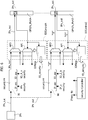
Figure 1 is generally illustrative of a circuit including IP-to-GPIO (IP = Intellectual Property; GPIO = General Purpose Input/Output) data-paths. - In such an arrangement, considering e.g. IPx as a reference, its output IPx_out may be physically connected to several Digital IO controllers (IOControl blocks), such as for example IOControlA... IOControlZ, which may be responsible for managing register driving and signal routing for a GPIO.
- For instance a Digital IO Controllers IOControl block may implement the selection of different data sources received as an input. The selection may be achieved e.g. through multiplexing via AFO (Alternate Function in Output) blocks, as connected to a specific GPIO output, indicated as GPIOAn_out... GPIOZn_out.
- A signal IPx_in sent as an input to the IPx block may be selected among various possible data sources available, e.g. as coming from the IOControl blocks.
- In this case, the IOControl blocks may perform GPIO input de-multiplexing through AFI (Alternate Function in Input) blocks to different destinations GPIOAn_in... GPIOZn_in.
- Similar considerations apply for e.g. a block IPy shown in the figure.
- The selection logic in the GPIO Controllers for multiplexing/de-multiplexing data sources may be controlled by programmable register blocks IORegs that facilitate software control of the IP-GPIO signal routing.
- For instance, a software control capability already available in the GPIO Controllers (in connection with the fact that communication may be active only between one source and one destination) may facilitate a low-cost implementation of the IP de-multiplexing feature.
- The IP output may be connected directly to the GPIO Controllers (without the need of any selection logic) and the IP input may be obtained as an hardwired OR combination of possible inputs coming from the GPIO Controllers (that is without any selection logic needed, because there is only one input active at any time).
- This may facilitate achieving IP-to-GPIO Controller data-paths that are, at the same time, faster and area-saving.
- Reasonable security requirements (and intended extension of security coverage to the IP-GPIO data-paths) may suggest an approach where the start and end points of a communication channel (i.e. the IP's and the GPIO's respectively) are made secure.
- For example, this approach may involve implementing two hardware components:
- a Security/Protection Digital IO Controller, programmable by a (secure) software application, that qualifies which ones of IPs in the Soc will be considered secure and not secure, respectively, and
- GPIO Digital IO Controllers (such as the IOControl blocks of
Figure 1 , each managing a group of GPIO's) programmable by secure software applications, e.g. via embedded registers, such as IORegs ofFigure 1 , in order to distinguish between secure and non secure GPIO's. - It was observed that, while effective for a single, point-to-point connection between IP and GPIO, such a solution may turn out to be inadequate with a SoC architecture, wherein IP-to-multiple GPIO's connectivity may be desirable, as in the case of a general purpose micro-controller.
- As shown in
Figure 2 , the output of a secure IP, like for example IPx, may be routed both to a secure GPIO (for example the one belonging to PortA) and to other GPIO's that can be non-secure (for example IO's on PortZ). - For instance,
Figure 2 shows a hypothetical secure output "spying" scenario through a non-secure connection. Moreover, the signal IPx_out on a path such as 10 may represent a secure data over a non-secure route; this means that a malicious software could be able to spy information transmitted over an "assumed" secure connection by programming the Digital IO Controller, like IOControlZ, of a non-secure GPIO in order, for example, to force the IO to feed back data received towards its input channel and allowing the Digital IO Controller to store it in the internal registers. In addition, malicious software can read the secure data by accessing the register through bus interface. The information over theline 20 may thus be read by software through a non-secure IP, while the information over theline 30 may be readable by software through register access. - In addition, as shown in
Figure 2 , the input of a secure IP, like for example IPx, may be represented not only by the signal coming from the secure GPIO, through IOControlA, but also by the hardwired combination of all the possible inputs from the GPIO's the IP is connected to.Figure 3 shows a secure input corruption scenario through non-secure connection (for example, the IO on PortZ in theFigure 3 ). - If one assumes that only one input may be active at a time, a malicious software may be able to corrupt information transmitted over the assumed secure connection, from GPIO to IP, by acting on the configuration of a IO Digital Controller of a non-secure GPIO, in order to force another data, for example the X_value on a
line 40, which may represent corrupting/corrupted data over a non-secure route (for example the IP input). This corrupted value X_value can came directly from the board, as indicated byreference 60, or from data written by malicious software through Digital IO Controller internal registers, as indicated byreference 50. - A possible approach in solving potential security issues related to an IP hardwired de-multiplexing feature, may involve connecting certain IPs, as required for secure connection, to only one of the available Digital IO Controllers and providing a fully secure architecture with all the GPIO's it controls.
- This solution may be helpful in avoiding secure transmission corruption and/or data spying but at the cost of:
- removing the de-multiplexing feature on some SoC IPs,
- reduced (virtually, lack of) flexibility in the IP-GPIOs mapping, because some IPs are mapped with a well specified Digital IO Controller,
- reduced (virtually, lack of) system configurability, because non-secure IPs with a de-multiplexing feature cannot be mapped onto Digital IO Controller and related GPIO's dedicated to secure IP's,
- limitations in resources available with different package options, and
- potential compatibility issues with previous product families where these IP-GPIO mapping limitations are not present.
- Another approach may involve replacing hardwired implementations of IP de-multiplexing features with a programmable multiplexer-based solution, controlled by secure registers, with the aim of performing a controlled selection of IP input/output routing with GPIO Controllers, avoiding risks as discussed previously.
- Although interesting from a logical viewpoint, this solution may end up by being expensive in terms of area requirements and timing performance degradation. These factors - in combination with the fact that a certain logic is already in place (e.g. embedded) in the GPIO Controllers - make such an approach less attractive from the SoC design perspective.
- One or more embodiments may provide a system including secure link connections, which are communication channels defined among Intellectual Property (IP) entities and multiple General Purpose Input/Output (GPIO) entities.
- In one or more embodiments, secure link connections may be provided by means of hardware components which are able to decide if a connection between a source and a destination can established (that is, should be allowed) or not (that is, denied or forbidden), in one or both directions.
- In one or more embodiments, such a decision may be taken on the basis of the security information status of the source and destination.
-
Figure 4 shows a schematic overview of IP-GPIO connections in a SoC sub-system embedding Secure Link hardware components to facilitate achieving security integrity. - In one or more embodiments, as exemplified in
Figure 4 , such a sort of "gating" control may be performed through the application of an hardware component (Secure Link) that may receive security information on an IP and a related GPIO and decide if the connection between the two entities could be established (allowed) or should be forbidden (denied), in either direction. - In the following, a first situation will be described by referring by way of example to a scenario involving a security application context.
- In one or more embodiments, a Secure Link component as discussed in the foregoing may be inserted in each connection between an IP and the corresponding GPIO's. In particular, thanks to de-multiplexing feature, the Secure Link component may control connections in both directions, i.e. the IP-to-GPIO and GPIO-to-IP paths.
- In one or more embodiments, this control may be dependent on the security status of the source and the destination of the communication channel (IP or GPIO, according to the transmission direction).
- In one or more embodiments, that information may be provided by some blocks already available in the security hardware infrastructure of a current SoC systems, that needs only to be fed to the Secure Link instances: the Security (Protection)
Controller 60 and the GPIO's Controllers. - In one or more embodiments, the
Security Controller 60 may define the secure/non-secure status of each IP in the SoC eligible for usage by applications running in a secure environment. This status, at the output of theSecurity Controller 60 is indicated in the figures by the label IP_Sec or IPSecurity. - In one or more embodiments, the GPIO Controllers provide secure/non-secure status of each GPIO, through its registers. This status is indicated in the figures by the label IO_sec or IOSecurity.
- In one or more embodiments, both the
Security Controller 60 and the GPIO Controllers may be programmable by software. - In one or more embodiments, by combining the information available, each Secure Link block may operate under conditions such as e.g.:
- allowing propagation of information between an IP and a GPIO, if both of them are configured as secure;
- allowing propagation of information between an IP and a GPIO, if both of them are configured as non-secure;
- denying propagation of information between an IP and a GPIO, if the IP is configured as secure but the GPIO is non-secure; and
- denying propagation of information between an IP and a GPIO, if the GPIO is configured as secure but the IP is non-secure.
- The scenario discussed in the foregoing provides a functional description of a possible implementation of the Secure Link component.
- In one or more embodiments, a Secure Link block can be defined according to the requirement of the application context in which is encapsulated.
- As an example,
Figure 5a shows a Secure Link block with inputs and outputs,Figure 5b shows a Secure Link low-cost implementation (reduced gate count), andFigure 5c shows an associated logical truth table. - In particular,
Figure 5b shows a logical control circuit, which comprises two AND logical port and an OR logical port. More in detail, each of the two AND logical port receives as a first input the signal IP_out or the signal IOCtrl_IN, and as second input the output of the OR logical port. The OR logical port receives in input the signal IP_sec inverted and the IO_sec signal. - In particular, the Secure Link block gives as outputs the following signals:
- IP_in=(IOCtrl_in) AND (IP_sec OR IO_sec)
- IOCtrl_out=(IP_out) AND (IP_sec OR IO_sec)
- The truth table in
Figure 5c shows the value of the output of the Secure Link block, in which communication between IP and GPIO is allowed not only when both IP and GPIO are secure or not secure, but also in the case of non-secure IP connected to secure GPIO. - This implementation may be based on the assumption that the GPIO Controller, which has the control of the GPIO status, is able to avoid connection between that IP and the secure GPIO, through the action of the internal multiplexing logic dedicated to the secure GPIO. In particular, the internal multiplexing logic dedicated to the secure GPIO is managed by programmable secure registers, thus acting under the control of secure software.
- As already mentioned, the Secure Link components do not need to be placed on every IP-GPIO physical link, but may be implemented (only) on those connections that could interface with start and end points exposed to potentially different security status during application execution.
- For example, IP and GPIO's with the same secure/non-secure status transitions do not need to be protected by a Secure Link block.
- Moreover, non-secure GPIO's expected never to be connected to secure IP's do not need to be protected by a Secure Link block.
- Finally, a non-secure IP expected never to be connected to secure GPIO's does not need to be protected by the Secure Link block.
- This usage flexibility allows a system based on a Secure Link block concept to cover a wide spectrum of applications in which security is needed, from full general purpose, where all the possible IP-GPIO's connections are equipped with the Secure Link components, to low cost or special purpose cases, where a specific subset of IP's and GPIO's is selected to be security aware and therefore protected via the Secure Link block.
-
Figure 6 shows an another example of a SoC system based on a Secure Link concept. - For instance,
Figure 6 shows how a Secure Link block may protect a SoC against a possible attack carried out by means of malicious software trying to detect data transmission over a secure connection. The example assumes IPx and IO_A_n are secure, while IO_Z_k and related controller IOControlZ are non-secure. - In particular, the first Secure Link block may allow e.g. at 70 the propagation of the secure data over the channel, while the second Secure Link block may deny e.g. at 80 the propagation of secure data over the channel.
- According to the information on the security status of IPx and GPIO (e.g. IO_A_n), said status being provided respectively by the Security Controller and the GPIO Controller (for example IOControlA), the associated Secure Link block may allow at 70 communication between the two entities, having recognized them as both secure. At the same time, the Secure Link component placed on the other connection available towards IPx_out, thanks to de-multiplexing feature, may performs a same check and block at 80 propagation of IPx_out towards GPIO (IO_Z_k), through the GPIO Controller (IOControlZ), having recognized the latter as non-secure. For istance, the output of the second Secure Link block may be set to "0" for that purpose.
- In this way, the IPx output will not reach the non-secure GPIO Controller and will not be open to detection by malicious software acting e.g. on the programmable registers of said GPIO.
-
Figure 7 shows still another scenario wherein a SoC system may be protected against possible attacks carried out by means of malicious software trying to corrupt data transmission over a secure connection by using a Secure Link block. - In one or more embodiments as exemplified in
Figure 7 , a Secure Link component placed on the connection between IO_A_n GPIO and IPx may allow communication at 90, due to secure status of both; conversely, a Secure Link block placed on the IO_Z_n GPIO and IPx connection may block at 100 data transmission between the two, due to the IO_Z_n non-secure status, thus avoiding that potential corrupting data (X_value) can be injected through GPIO or GPIO Controller (IOControlZ) registers. For example, the corrupting data X_value can be written at 110 by software through register access. - In this way, the corrupted value X_value will not reach the input combination hardwired logic and IPx input cannot be corrupted.
- One or more embodiments may rely on the analysis of potential security issues inside SoC systems, with application of one or more embodiments adapted to be extended to other technical contexts where controllable hardware gating points, like Secure Link components, may provide an added value.
- As indicated, one possible field of application of one or more embodiments may include SoC's with internal hardware partitions, where embedded cores may access separate IP subsets.
- Such a scenario may also involve access to dedicated GPIO resources.
- A system according to one or more embodiments, with a IP de-multiplexing feature, may facilitate achieving an higher degree of flexibility in system reconfiguration.
-
Figure 8 is exemplary of one such embodiment, wherein IPx and IPy may be physically connected to a same GPIO, through GPIO's Controllers (IOControl's blocks) and through other components (e.g. so-called Partition Link blocks, suc ha designation being intended to distinguish their functionality over the Secure Link blocks in the embodiments discussed previously). - In this context, each Partition Link block may manage the same data-path connection (IP output towards GPIO output, GPIO input towards IP input) as before, with gatingof communication performed according to different information coming from the system.
- In this scenario the control may be driven by number of the partition to which the IP/GPIO belongs, by allowing the connection if both have a same partition number (meaning IP and GPIO are included in the same partition), and gating (e.g. denying) the connection if partition numbers are different.
- Partition information can be provided - in a manner known per se - by a specific SoC component (HW Partition Controller) programmable or hardware specified.
- In the case of programmability support by the Partition Controller, the adoption of a Partition Link solution ad discussed previously may facilitate implementing a dynamically reconfigurable partitioned system, making it possible to provide a SoC with different hardware partitions according to software configuration.
- Of course, without prejudice to the principles of the invention, the details of construction and the embodiments may vary widely with respect to what has been described and illustrated herein purely by way of example, without thereby departing from the extent of protection.
- The extent of protection is defined by the annexed claims.
Claims (10)
- A system comprising secure link connections, including communication channels between Intellectual Property (IP, IPx, IPy) entities and multiple General Purpose Input/Output (GPIO, GPIO'sPortA, GPIO'sPortZ) entities, wherein said secure link connections are achieved by means of hardware components (SecureLink) configured to decide if a connection between a source (IPx, IPy, GPIO'sPortA, GPIO'sPortZ) and a destination (GPIO'sPortA, GPIO'sPortZ, IPx, IPy) is allowed or denied, in one or both directions, wherein said decision is taken on the basis of a security information status of the source (IPx, IPy, GPIO'sPortA, GPIO'sPortZ) and destination (GPIO'sPortA, GPIO'sPortZ, IPx, IPy).
- The system according to claim 1, wherein said source is an Intellectual Property (IP, IPx, IPy) entity and said destination is a General Purpose Input/Output (GPIO, GPIO'sPortA, GPIO'sPortZ) entity, or vice-versa.
- The system according to claim 1 or claim 2, wherein said hardware components (SecureLink) are inserted in each connection or communication channel between a source (IPx, IPy, GPIO'sPortA, GPIO'sPortZ) and a destination (GPIO'sPortA, GPIO'sPortZ, IPx, IPy).
- The system according any of the previous claims, wherein said hardware components (SecureLink) are configured to control, preferably thanks to a de-multiplexing feature, the secure connections in both directions, either from a source (IPx, IPy, GPIO'sPortA, GPIO'sPortZ) to a destination (GPIO'sPortA, GPIO'sPortZ, IPx, IPy) and from a destination (GPIO'sPortA, GPIO'sPortZ, IPx, IPy) to a source (IPx, IPy, GPIO'sPortA, GPIO'sPortZ).
- The system according to any of the previous claims, wherein said security information status of the source (IPx, IPy, GPIO'sPortA, GPIO'sPortZ) and destination (GPIO'sPortA, GPIO'sPortZ, IPx, IPy) of the secure link connections are provided by blocks (Security Protection Controller 60, GPIO's Controller) included in the security hardware infrastructure of the system.
- The system according to claim 5, wherein a first block (Security Controller, 60) defines the secure/non-secure status (IP_sec, IPSecurity) of the Intellectual Property (IP, IPx, IPy) entities of the system eligible for use by applications running in a secure environment, and a second block (GPIO's Controller) provides the secure/non-secure status (IO_sec, IOSecurity) of the General Purpose Input/Output (GPIO, GPIO'sPortA, GPIO'sPortZ) entities.
- The system according to claim 6, wherein both the first (Security Controller, 60) and the second (GPIO's Controller) blocks are programmable by software.
- The system according any of the previous claims, wherein said hardware components (SecureLink) include logical control circuits comprising logical ports.
- The system according any of the previous claims, wherein the system is a System on Chip (SoC).
- A method of operating a system according to any of claims 1 to 9, the method including combining said secure/non-secure status information (IP_sec, IPSecurity, IO_sec, IOSecurity) and controlling said secure link connections under the following conditions:- allowing propagation of information between an Intellectual Property (IP, IPx, IPy) and a General Purpose Input/Output (GPIO, GPIO'sPortA, GPIO'sPortZ), if both of them are configured as secure;- allowing propagation of information between an Intellectual Property (IP, IPx, IPy) and a General Purpose Input/Output (GPIO, GPIO'sPortA, GPIO'sPortZ), if both of them are configured as non-secure;- denying propagation of information between an Intellectual Property (IP, IPx, IPy) and a General Purpose Input/Output (GPIO, GPIO'sPortA, GPIO'sPortZ), if the Intellectual Property (IP, IPx, IPy) is configured as secure but the General Purpose Input/Output (GPIO, GPIO'sPortA, GPIO'sPortZ) is non-secure; and- denying propagation of information between an Intellectual Property (IP, IPx, IPy) and a General Purpose Input/Output (GPIO, GPIO'sPortA, GPIO'sPortZ), if the General Purpose Input/Output (GPIO, GPIO'sPortA, GPIO'sPortZ) is configured as secure but the Intellectual Property (IP, IPx, IPy) is non-secure.
Priority Applications (4)
| Application Number | Priority Date | Filing Date | Title |
|---|---|---|---|
| EP17305250.7A EP3373183B1 (en) | 2017-03-09 | 2017-03-09 | System with soc connections among ip and multiple gpios, and corresponding method |
| CN201721260614.9U CN207380710U (en) | 2017-03-09 | 2017-09-28 | Integrated circuit and system |
| CN201710898491.XA CN108572938B (en) | 2017-03-09 | 2017-09-28 | System with secure SOC connection between IP and multiple GPIOs and corresponding method |
| US15/916,067 US11144678B2 (en) | 2017-03-09 | 2018-03-08 | System with secure SoC connections among IP and multiple GPIOs, and corresponding method |
Applications Claiming Priority (1)
| Application Number | Priority Date | Filing Date | Title |
|---|---|---|---|
| EP17305250.7A EP3373183B1 (en) | 2017-03-09 | 2017-03-09 | System with soc connections among ip and multiple gpios, and corresponding method |
Publications (2)
| Publication Number | Publication Date |
|---|---|
| EP3373183A1 true EP3373183A1 (en) | 2018-09-12 |
| EP3373183B1 EP3373183B1 (en) | 2020-10-28 |
Family
ID=58873748
Family Applications (1)
| Application Number | Title | Priority Date | Filing Date |
|---|---|---|---|
| EP17305250.7A Active EP3373183B1 (en) | 2017-03-09 | 2017-03-09 | System with soc connections among ip and multiple gpios, and corresponding method |
Country Status (3)
| Country | Link |
|---|---|
| US (1) | US11144678B2 (en) |
| EP (1) | EP3373183B1 (en) |
| CN (2) | CN108572938B (en) |
Cited By (1)
| Publication number | Priority date | Publication date | Assignee | Title |
|---|---|---|---|---|
| EP3866033A4 (en) * | 2018-10-12 | 2022-07-13 | Kabushiki Kaisha Toshiba | INFORMATION PROCESSING DEVICE AND INFORMATION PROCESSING SYSTEM |
Families Citing this family (70)
| Publication number | Priority date | Publication date | Assignee | Title |
|---|---|---|---|---|
| US12288233B2 (en) | 2016-04-01 | 2025-04-29 | OneTrust, LLC | Data processing systems and methods for integrating privacy information management systems with data loss prevention tools or other tools for privacy design |
| US10997318B2 (en) | 2016-06-10 | 2021-05-04 | OneTrust, LLC | Data processing systems for generating and populating a data inventory for processing data access requests |
| US11222142B2 (en) | 2016-06-10 | 2022-01-11 | OneTrust, LLC | Data processing systems for validating authorization for personal data collection, storage, and processing |
| US11134086B2 (en) | 2016-06-10 | 2021-09-28 | OneTrust, LLC | Consent conversion optimization systems and related methods |
| US12052289B2 (en) | 2016-06-10 | 2024-07-30 | OneTrust, LLC | Data processing systems for data-transfer risk identification, cross-border visualization generation, and related methods |
| US11727141B2 (en) | 2016-06-10 | 2023-08-15 | OneTrust, LLC | Data processing systems and methods for synching privacy-related user consent across multiple computing devices |
| US11416798B2 (en) | 2016-06-10 | 2022-08-16 | OneTrust, LLC | Data processing systems and methods for providing training in a vendor procurement process |
| US11675929B2 (en) | 2016-06-10 | 2023-06-13 | OneTrust, LLC | Data processing consent sharing systems and related methods |
| US11651106B2 (en) | 2016-06-10 | 2023-05-16 | OneTrust, LLC | Data processing systems for fulfilling data subject access requests and related methods |
| US12299065B2 (en) | 2016-06-10 | 2025-05-13 | OneTrust, LLC | Data processing systems and methods for dynamically determining data processing consent configurations |
| US12381915B2 (en) | 2016-06-10 | 2025-08-05 | OneTrust, LLC | Data processing systems and methods for performing assessments and monitoring of new versions of computer code for compliance |
| US11461500B2 (en) | 2016-06-10 | 2022-10-04 | OneTrust, LLC | Data processing systems for cookie compliance testing with website scanning and related methods |
| US12136055B2 (en) | 2016-06-10 | 2024-11-05 | OneTrust, LLC | Data processing systems for identifying, assessing, and remediating data processing risks using data modeling techniques |
| US10909265B2 (en) | 2016-06-10 | 2021-02-02 | OneTrust, LLC | Application privacy scanning systems and related methods |
| US11354434B2 (en) | 2016-06-10 | 2022-06-07 | OneTrust, LLC | Data processing systems for verification of consent and notice processing and related methods |
| US11418492B2 (en) | 2016-06-10 | 2022-08-16 | OneTrust, LLC | Data processing systems and methods for using a data model to select a target data asset in a data migration |
| US11438386B2 (en) | 2016-06-10 | 2022-09-06 | OneTrust, LLC | Data processing systems for data-transfer risk identification, cross-border visualization generation, and related methods |
| US11651104B2 (en) | 2016-06-10 | 2023-05-16 | OneTrust, LLC | Consent receipt management systems and related methods |
| US11392720B2 (en) | 2016-06-10 | 2022-07-19 | OneTrust, LLC | Data processing systems for verification of consent and notice processing and related methods |
| US11544667B2 (en) | 2016-06-10 | 2023-01-03 | OneTrust, LLC | Data processing systems for generating and populating a data inventory |
| US10685140B2 (en) | 2016-06-10 | 2020-06-16 | OneTrust, LLC | Consent receipt management systems and related methods |
| US11416590B2 (en) | 2016-06-10 | 2022-08-16 | OneTrust, LLC | Data processing and scanning systems for assessing vendor risk |
| US11586700B2 (en) | 2016-06-10 | 2023-02-21 | OneTrust, LLC | Data processing systems and methods for automatically blocking the use of tracking tools |
| US12045266B2 (en) * | 2016-06-10 | 2024-07-23 | OneTrust, LLC | Data processing systems for generating and populating a data inventory |
| US11636171B2 (en) | 2016-06-10 | 2023-04-25 | OneTrust, LLC | Data processing user interface monitoring systems and related methods |
| US11366909B2 (en) | 2016-06-10 | 2022-06-21 | OneTrust, LLC | Data processing and scanning systems for assessing vendor risk |
| US10846433B2 (en) | 2016-06-10 | 2020-11-24 | OneTrust, LLC | Data processing consent management systems and related methods |
| US12591828B2 (en) | 2016-06-10 | 2026-03-31 | OneTrust, LLC | Data processing systems for fulfilling data subject access requests and related methods |
| US11188615B2 (en) | 2016-06-10 | 2021-11-30 | OneTrust, LLC | Data processing consent capture systems and related methods |
| US11416589B2 (en) | 2016-06-10 | 2022-08-16 | OneTrust, LLC | Data processing and scanning systems for assessing vendor risk |
| US12118121B2 (en) | 2016-06-10 | 2024-10-15 | OneTrust, LLC | Data subject access request processing systems and related methods |
| US11354435B2 (en) | 2016-06-10 | 2022-06-07 | OneTrust, LLC | Data processing systems for data testing to confirm data deletion and related methods |
| US10318761B2 (en) | 2016-06-10 | 2019-06-11 | OneTrust, LLC | Data processing systems and methods for auditing data request compliance |
| US11481710B2 (en) | 2016-06-10 | 2022-10-25 | OneTrust, LLC | Privacy management systems and methods |
| US11188862B2 (en) | 2016-06-10 | 2021-11-30 | OneTrust, LLC | Privacy management systems and methods |
| US11520928B2 (en) | 2016-06-10 | 2022-12-06 | OneTrust, LLC | Data processing systems for generating personal data receipts and related methods |
| US11416109B2 (en) | 2016-06-10 | 2022-08-16 | OneTrust, LLC | Automated data processing systems and methods for automatically processing data subject access requests using a chatbot |
| US11562097B2 (en) | 2016-06-10 | 2023-01-24 | OneTrust, LLC | Data processing systems for central consent repository and related methods |
| US11294939B2 (en) | 2016-06-10 | 2022-04-05 | OneTrust, LLC | Data processing systems and methods for automatically detecting and documenting privacy-related aspects of computer software |
| US11475136B2 (en) | 2016-06-10 | 2022-10-18 | OneTrust, LLC | Data processing systems for data transfer risk identification and related methods |
| US11222139B2 (en) | 2016-06-10 | 2022-01-11 | OneTrust, LLC | Data processing systems and methods for automatic discovery and assessment of mobile software development kits |
| US11295316B2 (en) | 2016-06-10 | 2022-04-05 | OneTrust, LLC | Data processing systems for identity validation for consumer rights requests and related methods |
| US10909488B2 (en) | 2016-06-10 | 2021-02-02 | OneTrust, LLC | Data processing systems for assessing readiness for responding to privacy-related incidents |
| US11625502B2 (en) | 2016-06-10 | 2023-04-11 | OneTrust, LLC | Data processing systems for identifying and modifying processes that are subject to data subject access requests |
| US10284604B2 (en) | 2016-06-10 | 2019-05-07 | OneTrust, LLC | Data processing and scanning systems for generating and populating a data inventory |
| US11403377B2 (en) | 2016-06-10 | 2022-08-02 | OneTrust, LLC | Privacy management systems and methods |
| US11227247B2 (en) | 2016-06-10 | 2022-01-18 | OneTrust, LLC | Data processing systems and methods for bundled privacy policies |
| US10013577B1 (en) | 2017-06-16 | 2018-07-03 | OneTrust, LLC | Data processing systems for identifying whether cookies contain personally identifying information |
| US10496582B1 (en) * | 2018-09-06 | 2019-12-03 | Mellanox Technologies, Ltd. | Flexible multi-domain GPIO expansion |
| US10803202B2 (en) | 2018-09-07 | 2020-10-13 | OneTrust, LLC | Data processing systems for orphaned data identification and deletion and related methods |
| US11544409B2 (en) | 2018-09-07 | 2023-01-03 | OneTrust, LLC | Data processing systems and methods for automatically protecting sensitive data within privacy management systems |
| US11797528B2 (en) | 2020-07-08 | 2023-10-24 | OneTrust, LLC | Systems and methods for targeted data discovery |
| EP4189569B1 (en) | 2020-07-28 | 2025-09-24 | OneTrust LLC | Systems and methods for automatically blocking the use of tracking tools |
| CN112182998B (en) * | 2020-07-29 | 2024-08-30 | 北京智芯微电子科技有限公司 | Object-oriented chip-level port interconnection circuit and port interconnection method thereof |
| US11475165B2 (en) | 2020-08-06 | 2022-10-18 | OneTrust, LLC | Data processing systems and methods for automatically redacting unstructured data from a data subject access request |
| WO2022060860A1 (en) | 2020-09-15 | 2022-03-24 | OneTrust, LLC | Data processing systems and methods for detecting tools for the automatic blocking of consent requests |
| US11526624B2 (en) | 2020-09-21 | 2022-12-13 | OneTrust, LLC | Data processing systems and methods for automatically detecting target data transfers and target data processing |
| US12265896B2 (en) | 2020-10-05 | 2025-04-01 | OneTrust, LLC | Systems and methods for detecting prejudice bias in machine-learning models |
| US11397819B2 (en) | 2020-11-06 | 2022-07-26 | OneTrust, LLC | Systems and methods for identifying data processing activities based on data discovery results |
| WO2022159901A1 (en) | 2021-01-25 | 2022-07-28 | OneTrust, LLC | Systems and methods for discovery, classification, and indexing of data in a native computing system |
| US11442906B2 (en) | 2021-02-04 | 2022-09-13 | OneTrust, LLC | Managing custom attributes for domain objects defined within microservices |
| WO2022170254A1 (en) | 2021-02-08 | 2022-08-11 | OneTrust, LLC | Data processing systems and methods for anonymizing data samples in classification analysis |
| US11601464B2 (en) | 2021-02-10 | 2023-03-07 | OneTrust, LLC | Systems and methods for mitigating risks of third-party computing system functionality integration into a first-party computing system |
| WO2022178089A1 (en) | 2021-02-17 | 2022-08-25 | OneTrust, LLC | Managing custom workflows for domain objects defined within microservices |
| WO2022178219A1 (en) | 2021-02-18 | 2022-08-25 | OneTrust, LLC | Selective redaction of media content |
| EP4305539A1 (en) | 2021-03-08 | 2024-01-17 | OneTrust, LLC | Data transfer discovery and analysis systems and related methods |
| US11562078B2 (en) | 2021-04-16 | 2023-01-24 | OneTrust, LLC | Assessing and managing computational risk involved with integrating third party computing functionality within a computing system |
| US12153704B2 (en) | 2021-08-05 | 2024-11-26 | OneTrust, LLC | Computing platform for facilitating data exchange among computing environments |
| US11620142B1 (en) | 2022-06-03 | 2023-04-04 | OneTrust, LLC | Generating and customizing user interfaces for demonstrating functions of interactive user environments |
| CN117134765B (en) * | 2023-08-24 | 2024-06-07 | 毫厘智能科技(江苏)有限公司 | Circuit and chip with reconfigurable inter-chip connection structure |
Citations (4)
| Publication number | Priority date | Publication date | Assignee | Title |
|---|---|---|---|---|
| US6138240A (en) * | 1998-06-19 | 2000-10-24 | Compaq Computer Corporation | Secure general purpose input/output pins for protecting computer system resources |
| US20140082237A1 (en) * | 2012-09-20 | 2014-03-20 | Aviad Wertheimer | Run-time fabric reconfiguration |
| US20140137231A1 (en) * | 2011-12-21 | 2014-05-15 | Manoj R. Sastry | INCORPORATING ACCESS CONTROL FUNCTIONALITY INTO A SYSTEM ON A CHIP (SoC) |
| US20160180114A1 (en) * | 2014-12-19 | 2016-06-23 | Intel Corporation | Security plugin for a system-on-a-chip platform |
Family Cites Families (9)
| Publication number | Priority date | Publication date | Assignee | Title |
|---|---|---|---|---|
| US20030108205A1 (en) * | 2001-12-07 | 2003-06-12 | Bryan Joyner | System and method for providing encrypted data to a device |
| US20070168574A1 (en) * | 2005-09-28 | 2007-07-19 | Dell Products L.P. | System and method for securing access to general purpose input/output ports in a computer system |
| US8370605B2 (en) * | 2009-11-11 | 2013-02-05 | Sunman Engineering, Inc. | Computer architecture for a mobile communication platform |
| US8427193B1 (en) * | 2010-12-07 | 2013-04-23 | Xilinx, Inc. | Intellectual property core protection for integrated circuits |
| CN102752104B (en) * | 2012-06-07 | 2017-10-31 | 中国电子科技集团公司第三十研究所 | A kind of symmetric cryptography service implementing method based on smart card COS |
| CN103077362B (en) * | 2012-12-27 | 2015-09-30 | 深圳先进技术研究院 | There is the GPIO IP kernel of security mechanism |
| CN204066121U (en) * | 2013-10-31 | 2014-12-31 | 中国大唐集团财务有限公司 | A kind of PCI-E encrypted card |
| CN104135410A (en) * | 2014-06-20 | 2014-11-05 | 浙江中控研究院有限公司 | EPA (Ethernet for Plant Automation) communication IP (Intellectual Property) core and system on chip (SOC) based on AMBA (Advanced Microcontroller Bus Architecture) bus structure |
| CN106250725A (en) * | 2016-08-02 | 2016-12-21 | 浪潮电子信息产业股份有限公司 | A method for preventing UEFI program from being illegally transplanted on ARM platform |
-
2017
- 2017-03-09 EP EP17305250.7A patent/EP3373183B1/en active Active
- 2017-09-28 CN CN201710898491.XA patent/CN108572938B/en active Active
- 2017-09-28 CN CN201721260614.9U patent/CN207380710U/en active Active
-
2018
- 2018-03-08 US US15/916,067 patent/US11144678B2/en active Active
Patent Citations (4)
| Publication number | Priority date | Publication date | Assignee | Title |
|---|---|---|---|---|
| US6138240A (en) * | 1998-06-19 | 2000-10-24 | Compaq Computer Corporation | Secure general purpose input/output pins for protecting computer system resources |
| US20140137231A1 (en) * | 2011-12-21 | 2014-05-15 | Manoj R. Sastry | INCORPORATING ACCESS CONTROL FUNCTIONALITY INTO A SYSTEM ON A CHIP (SoC) |
| US20140082237A1 (en) * | 2012-09-20 | 2014-03-20 | Aviad Wertheimer | Run-time fabric reconfiguration |
| US20160180114A1 (en) * | 2014-12-19 | 2016-06-23 | Intel Corporation | Security plugin for a system-on-a-chip platform |
Cited By (1)
| Publication number | Priority date | Publication date | Assignee | Title |
|---|---|---|---|---|
| EP3866033A4 (en) * | 2018-10-12 | 2022-07-13 | Kabushiki Kaisha Toshiba | INFORMATION PROCESSING DEVICE AND INFORMATION PROCESSING SYSTEM |
Also Published As
| Publication number | Publication date |
|---|---|
| US11144678B2 (en) | 2021-10-12 |
| CN108572938A (en) | 2018-09-25 |
| EP3373183B1 (en) | 2020-10-28 |
| US20180260585A1 (en) | 2018-09-13 |
| CN108572938B (en) | 2022-06-24 |
| CN207380710U (en) | 2018-05-18 |
Similar Documents
| Publication | Publication Date | Title |
|---|---|---|
| EP3373183B1 (en) | System with soc connections among ip and multiple gpios, and corresponding method | |
| US12547569B2 (en) | Flexible mobile device connectivity to automotive systems with USB hubs | |
| Diguet et al. | NOC-centric security of reconfigurable SoC | |
| EP2173060B1 (en) | Virtualized secure networking | |
| KR20140081809A (en) | Virtual general purpose input/output for a microcontroller | |
| CA2446983A1 (en) | Programmable logic device including programmable interface core and central processing unit | |
| US8527675B2 (en) | System and method for implementing a secure processor data bus | |
| US20220164485A1 (en) | Method and configurable hardware module for monitoring a hardware-application | |
| CN108959138B (en) | System comprising intellectual property circuits in communication with general input/output pads, corresponding apparatus and method | |
| US8970248B2 (en) | Sharing hardware resources between D-PHY and N-factorial termination networks | |
| US12086083B2 (en) | Multi-tenant aware data processing units | |
| KR100426304B1 (en) | Smart card emulator and emulation method thereof | |
| CN216118784U (en) | Bidirectional pin multifunctional multiplexing circuit, FPGA device and multifunctional multiplexing system | |
| US20210303315A1 (en) | Application logic architecture defining separate processing planes | |
| CN117009285A (en) | System on chip integrated with direct memory access circuit and corresponding method | |
| Boden et al. | A low-cost realization of an adaptable protocol processing unit | |
| KR101098381B1 (en) | Network Interface Card including port switching circuit |
Legal Events
| Date | Code | Title | Description |
|---|---|---|---|
| PUAI | Public reference made under article 153(3) epc to a published international application that has entered the european phase |
Free format text: ORIGINAL CODE: 0009012 |
|
| STAA | Information on the status of an ep patent application or granted ep patent |
Free format text: STATUS: REQUEST FOR EXAMINATION WAS MADE |
|
| 17P | Request for examination filed |
Effective date: 20170309 |
|
| AK | Designated contracting states |
Kind code of ref document: A1 Designated state(s): AL AT BE BG CH CY CZ DE DK EE ES FI FR GB GR HR HU IE IS IT LI LT LU LV MC MK MT NL NO PL PT RO RS SE SI SK SM TR |
|
| AX | Request for extension of the european patent |
Extension state: BA ME |
|
| GRAP | Despatch of communication of intention to grant a patent |
Free format text: ORIGINAL CODE: EPIDOSNIGR1 |
|
| STAA | Information on the status of an ep patent application or granted ep patent |
Free format text: STATUS: GRANT OF PATENT IS INTENDED |
|
| RIC1 | Information provided on ipc code assigned before grant |
Ipc: G06F 13/40 20060101ALI20200302BHEP Ipc: G06F 21/76 20130101ALI20200302BHEP Ipc: G06F 21/60 20130101AFI20200302BHEP |
|
| INTG | Intention to grant announced |
Effective date: 20200406 |
|
| GRAJ | Information related to disapproval of communication of intention to grant by the applicant or resumption of examination proceedings by the epo deleted |
Free format text: ORIGINAL CODE: EPIDOSDIGR1 |
|
| STAA | Information on the status of an ep patent application or granted ep patent |
Free format text: STATUS: REQUEST FOR EXAMINATION WAS MADE |
|
| GRAP | Despatch of communication of intention to grant a patent |
Free format text: ORIGINAL CODE: EPIDOSNIGR1 |
|
| STAA | Information on the status of an ep patent application or granted ep patent |
Free format text: STATUS: GRANT OF PATENT IS INTENDED |
|
| INTC | Intention to grant announced (deleted) | ||
| INTG | Intention to grant announced |
Effective date: 20200608 |
|
| GRAS | Grant fee paid |
Free format text: ORIGINAL CODE: EPIDOSNIGR3 |
|
| GRAA | (expected) grant |
Free format text: ORIGINAL CODE: 0009210 |
|
| STAA | Information on the status of an ep patent application or granted ep patent |
Free format text: STATUS: THE PATENT HAS BEEN GRANTED |
|
| AK | Designated contracting states |
Kind code of ref document: B1 Designated state(s): AL AT BE BG CH CY CZ DE DK EE ES FI FR GB GR HR HU IE IS IT LI LT LU LV MC MK MT NL NO PL PT RO RS SE SI SK SM TR |
|
| REG | Reference to a national code |
Ref country code: GB Ref legal event code: FG4D |
|
| REG | Reference to a national code |
Ref country code: CH Ref legal event code: EP |
|
| REG | Reference to a national code |
Ref country code: AT Ref legal event code: REF Ref document number: 1328938 Country of ref document: AT Kind code of ref document: T Effective date: 20201115 |
|
| REG | Reference to a national code |
Ref country code: DE Ref legal event code: R096 Ref document number: 602017026267 Country of ref document: DE |
|
| REG | Reference to a national code |
Ref country code: IE Ref legal event code: FG4D |
|
| REG | Reference to a national code |
Ref country code: AT Ref legal event code: MK05 Ref document number: 1328938 Country of ref document: AT Kind code of ref document: T Effective date: 20201028 |
|
| REG | Reference to a national code |
Ref country code: NL Ref legal event code: MP Effective date: 20201028 |
|
| PG25 | Lapsed in a contracting state [announced via postgrant information from national office to epo] |
Ref country code: RS Free format text: LAPSE BECAUSE OF FAILURE TO SUBMIT A TRANSLATION OF THE DESCRIPTION OR TO PAY THE FEE WITHIN THE PRESCRIBED TIME-LIMIT Effective date: 20201028 Ref country code: PT Free format text: LAPSE BECAUSE OF FAILURE TO SUBMIT A TRANSLATION OF THE DESCRIPTION OR TO PAY THE FEE WITHIN THE PRESCRIBED TIME-LIMIT Effective date: 20210301 Ref country code: NO Free format text: LAPSE BECAUSE OF FAILURE TO SUBMIT A TRANSLATION OF THE DESCRIPTION OR TO PAY THE FEE WITHIN THE PRESCRIBED TIME-LIMIT Effective date: 20210128 Ref country code: FI Free format text: LAPSE BECAUSE OF FAILURE TO SUBMIT A TRANSLATION OF THE DESCRIPTION OR TO PAY THE FEE WITHIN THE PRESCRIBED TIME-LIMIT Effective date: 20201028 Ref country code: GR Free format text: LAPSE BECAUSE OF FAILURE TO SUBMIT A TRANSLATION OF THE DESCRIPTION OR TO PAY THE FEE WITHIN THE PRESCRIBED TIME-LIMIT Effective date: 20210129 |
|
| REG | Reference to a national code |
Ref country code: LT Ref legal event code: MG4D |
|
| PG25 | Lapsed in a contracting state [announced via postgrant information from national office to epo] |
Ref country code: IS Free format text: LAPSE BECAUSE OF FAILURE TO SUBMIT A TRANSLATION OF THE DESCRIPTION OR TO PAY THE FEE WITHIN THE PRESCRIBED TIME-LIMIT Effective date: 20210228 Ref country code: PL Free format text: LAPSE BECAUSE OF FAILURE TO SUBMIT A TRANSLATION OF THE DESCRIPTION OR TO PAY THE FEE WITHIN THE PRESCRIBED TIME-LIMIT Effective date: 20201028 Ref country code: LV Free format text: LAPSE BECAUSE OF FAILURE TO SUBMIT A TRANSLATION OF THE DESCRIPTION OR TO PAY THE FEE WITHIN THE PRESCRIBED TIME-LIMIT Effective date: 20201028 Ref country code: BG Free format text: LAPSE BECAUSE OF FAILURE TO SUBMIT A TRANSLATION OF THE DESCRIPTION OR TO PAY THE FEE WITHIN THE PRESCRIBED TIME-LIMIT Effective date: 20210128 Ref country code: AT Free format text: LAPSE BECAUSE OF FAILURE TO SUBMIT A TRANSLATION OF THE DESCRIPTION OR TO PAY THE FEE WITHIN THE PRESCRIBED TIME-LIMIT Effective date: 20201028 Ref country code: ES Free format text: LAPSE BECAUSE OF FAILURE TO SUBMIT A TRANSLATION OF THE DESCRIPTION OR TO PAY THE FEE WITHIN THE PRESCRIBED TIME-LIMIT Effective date: 20201028 Ref country code: SE Free format text: LAPSE BECAUSE OF FAILURE TO SUBMIT A TRANSLATION OF THE DESCRIPTION OR TO PAY THE FEE WITHIN THE PRESCRIBED TIME-LIMIT Effective date: 20201028 |
|
| PG25 | Lapsed in a contracting state [announced via postgrant information from national office to epo] |
Ref country code: HR Free format text: LAPSE BECAUSE OF FAILURE TO SUBMIT A TRANSLATION OF THE DESCRIPTION OR TO PAY THE FEE WITHIN THE PRESCRIBED TIME-LIMIT Effective date: 20201028 Ref country code: NL Free format text: LAPSE BECAUSE OF FAILURE TO SUBMIT A TRANSLATION OF THE DESCRIPTION OR TO PAY THE FEE WITHIN THE PRESCRIBED TIME-LIMIT Effective date: 20201028 |
|
| REG | Reference to a national code |
Ref country code: DE Ref legal event code: R097 Ref document number: 602017026267 Country of ref document: DE |
|
| PG25 | Lapsed in a contracting state [announced via postgrant information from national office to epo] |
Ref country code: RO Free format text: LAPSE BECAUSE OF FAILURE TO SUBMIT A TRANSLATION OF THE DESCRIPTION OR TO PAY THE FEE WITHIN THE PRESCRIBED TIME-LIMIT Effective date: 20201028 Ref country code: SK Free format text: LAPSE BECAUSE OF FAILURE TO SUBMIT A TRANSLATION OF THE DESCRIPTION OR TO PAY THE FEE WITHIN THE PRESCRIBED TIME-LIMIT Effective date: 20201028 Ref country code: SM Free format text: LAPSE BECAUSE OF FAILURE TO SUBMIT A TRANSLATION OF THE DESCRIPTION OR TO PAY THE FEE WITHIN THE PRESCRIBED TIME-LIMIT Effective date: 20201028 Ref country code: EE Free format text: LAPSE BECAUSE OF FAILURE TO SUBMIT A TRANSLATION OF THE DESCRIPTION OR TO PAY THE FEE WITHIN THE PRESCRIBED TIME-LIMIT Effective date: 20201028 Ref country code: CZ Free format text: LAPSE BECAUSE OF FAILURE TO SUBMIT A TRANSLATION OF THE DESCRIPTION OR TO PAY THE FEE WITHIN THE PRESCRIBED TIME-LIMIT Effective date: 20201028 Ref country code: LT Free format text: LAPSE BECAUSE OF FAILURE TO SUBMIT A TRANSLATION OF THE DESCRIPTION OR TO PAY THE FEE WITHIN THE PRESCRIBED TIME-LIMIT Effective date: 20201028 |
|
| PG25 | Lapsed in a contracting state [announced via postgrant information from national office to epo] |
Ref country code: DK Free format text: LAPSE BECAUSE OF FAILURE TO SUBMIT A TRANSLATION OF THE DESCRIPTION OR TO PAY THE FEE WITHIN THE PRESCRIBED TIME-LIMIT Effective date: 20201028 |
|
| PLBE | No opposition filed within time limit |
Free format text: ORIGINAL CODE: 0009261 |
|
| STAA | Information on the status of an ep patent application or granted ep patent |
Free format text: STATUS: NO OPPOSITION FILED WITHIN TIME LIMIT |
|
| 26N | No opposition filed |
Effective date: 20210729 |
|
| PG25 | Lapsed in a contracting state [announced via postgrant information from national office to epo] |
Ref country code: AL Free format text: LAPSE BECAUSE OF FAILURE TO SUBMIT A TRANSLATION OF THE DESCRIPTION OR TO PAY THE FEE WITHIN THE PRESCRIBED TIME-LIMIT Effective date: 20201028 Ref country code: MC Free format text: LAPSE BECAUSE OF FAILURE TO SUBMIT A TRANSLATION OF THE DESCRIPTION OR TO PAY THE FEE WITHIN THE PRESCRIBED TIME-LIMIT Effective date: 20201028 Ref country code: IT Free format text: LAPSE BECAUSE OF FAILURE TO SUBMIT A TRANSLATION OF THE DESCRIPTION OR TO PAY THE FEE WITHIN THE PRESCRIBED TIME-LIMIT Effective date: 20201028 |
|
| REG | Reference to a national code |
Ref country code: CH Ref legal event code: PL |
|
| GBPC | Gb: european patent ceased through non-payment of renewal fee |
Effective date: 20210309 |
|
| PG25 | Lapsed in a contracting state [announced via postgrant information from national office to epo] |
Ref country code: SI Free format text: LAPSE BECAUSE OF FAILURE TO SUBMIT A TRANSLATION OF THE DESCRIPTION OR TO PAY THE FEE WITHIN THE PRESCRIBED TIME-LIMIT Effective date: 20201028 |
|
| REG | Reference to a national code |
Ref country code: BE Ref legal event code: MM Effective date: 20210331 |
|
| PG25 | Lapsed in a contracting state [announced via postgrant information from national office to epo] |
Ref country code: CH Free format text: LAPSE BECAUSE OF NON-PAYMENT OF DUE FEES Effective date: 20210331 Ref country code: LU Free format text: LAPSE BECAUSE OF NON-PAYMENT OF DUE FEES Effective date: 20210309 Ref country code: LI Free format text: LAPSE BECAUSE OF NON-PAYMENT OF DUE FEES Effective date: 20210331 Ref country code: IE Free format text: LAPSE BECAUSE OF NON-PAYMENT OF DUE FEES Effective date: 20210309 Ref country code: FR Free format text: LAPSE BECAUSE OF NON-PAYMENT OF DUE FEES Effective date: 20210331 Ref country code: GB Free format text: LAPSE BECAUSE OF NON-PAYMENT OF DUE FEES Effective date: 20210309 |
|
| PG25 | Lapsed in a contracting state [announced via postgrant information from national office to epo] |
Ref country code: IS Free format text: LAPSE BECAUSE OF FAILURE TO SUBMIT A TRANSLATION OF THE DESCRIPTION OR TO PAY THE FEE WITHIN THE PRESCRIBED TIME-LIMIT Effective date: 20210228 |
|
| PG25 | Lapsed in a contracting state [announced via postgrant information from national office to epo] |
Ref country code: BE Free format text: LAPSE BECAUSE OF NON-PAYMENT OF DUE FEES Effective date: 20210331 |
|
| PG25 | Lapsed in a contracting state [announced via postgrant information from national office to epo] |
Ref country code: CY Free format text: LAPSE BECAUSE OF FAILURE TO SUBMIT A TRANSLATION OF THE DESCRIPTION OR TO PAY THE FEE WITHIN THE PRESCRIBED TIME-LIMIT Effective date: 20201028 |
|
| PG25 | Lapsed in a contracting state [announced via postgrant information from national office to epo] |
Ref country code: HU Free format text: LAPSE BECAUSE OF FAILURE TO SUBMIT A TRANSLATION OF THE DESCRIPTION OR TO PAY THE FEE WITHIN THE PRESCRIBED TIME-LIMIT; INVALID AB INITIO Effective date: 20170309 |
|
| PG25 | Lapsed in a contracting state [announced via postgrant information from national office to epo] |
Ref country code: MK Free format text: LAPSE BECAUSE OF FAILURE TO SUBMIT A TRANSLATION OF THE DESCRIPTION OR TO PAY THE FEE WITHIN THE PRESCRIBED TIME-LIMIT Effective date: 20201028 |
|
| PG25 | Lapsed in a contracting state [announced via postgrant information from national office to epo] |
Ref country code: MT Free format text: LAPSE BECAUSE OF FAILURE TO SUBMIT A TRANSLATION OF THE DESCRIPTION OR TO PAY THE FEE WITHIN THE PRESCRIBED TIME-LIMIT Effective date: 20201028 |
|
| PGFP | Annual fee paid to national office [announced via postgrant information from national office to epo] |
Ref country code: DE Payment date: 20250218 Year of fee payment: 9 |
|
| PG25 | Lapsed in a contracting state [announced via postgrant information from national office to epo] |
Ref country code: TR Free format text: LAPSE BECAUSE OF FAILURE TO SUBMIT A TRANSLATION OF THE DESCRIPTION OR TO PAY THE FEE WITHIN THE PRESCRIBED TIME-LIMIT Effective date: 20201028 |