EP3373150A1 - Methods of accessing memory cells, methods of distributing memory requests, systems, and memory controllers - Google Patents
Methods of accessing memory cells, methods of distributing memory requests, systems, and memory controllers Download PDFInfo
- Publication number
- EP3373150A1 EP3373150A1 EP18170452.9A EP18170452A EP3373150A1 EP 3373150 A1 EP3373150 A1 EP 3373150A1 EP 18170452 A EP18170452 A EP 18170452A EP 3373150 A1 EP3373150 A1 EP 3373150A1
- Authority
- EP
- European Patent Office
- Prior art keywords
- memory
- address
- region
- channel
- request
- Prior art date
- Legal status (The legal status is an assumption and is not a legal conclusion. Google has not performed a legal analysis and makes no representation as to the accuracy of the status listed.)
- Granted
Links
Images





Classifications
-
- G—PHYSICS
- G06—COMPUTING OR CALCULATING; COUNTING
- G06F—ELECTRIC DIGITAL DATA PROCESSING
- G06F12/00—Accessing, addressing or allocating within memory systems or architectures
- G06F12/02—Addressing or allocation; Relocation
-
- G—PHYSICS
- G06—COMPUTING OR CALCULATING; COUNTING
- G06F—ELECTRIC DIGITAL DATA PROCESSING
- G06F12/00—Accessing, addressing or allocating within memory systems or architectures
- G06F12/02—Addressing or allocation; Relocation
- G06F12/06—Addressing a physical block of locations, e.g. base addressing, module addressing, memory dedication
-
- G—PHYSICS
- G06—COMPUTING OR CALCULATING; COUNTING
- G06F—ELECTRIC DIGITAL DATA PROCESSING
- G06F12/00—Accessing, addressing or allocating within memory systems or architectures
- G06F12/02—Addressing or allocation; Relocation
- G06F12/06—Addressing a physical block of locations, e.g. base addressing, module addressing, memory dedication
- G06F12/0646—Configuration or reconfiguration
- G06F12/0653—Configuration or reconfiguration with centralised address assignment
-
- G—PHYSICS
- G06—COMPUTING OR CALCULATING; COUNTING
- G06F—ELECTRIC DIGITAL DATA PROCESSING
- G06F13/00—Interconnection of, or transfer of information or other signals between, memories, input/output devices or central processing units
- G06F13/14—Handling requests for interconnection or transfer
-
- G—PHYSICS
- G06—COMPUTING OR CALCULATING; COUNTING
- G06F—ELECTRIC DIGITAL DATA PROCESSING
- G06F13/00—Interconnection of, or transfer of information or other signals between, memories, input/output devices or central processing units
- G06F13/14—Handling requests for interconnection or transfer
- G06F13/16—Handling requests for interconnection or transfer for access to memory bus
-
- G—PHYSICS
- G06—COMPUTING OR CALCULATING; COUNTING
- G06F—ELECTRIC DIGITAL DATA PROCESSING
- G06F3/00—Input arrangements for transferring data to be processed into a form capable of being handled by the computer; Output arrangements for transferring data from processing unit to output unit, e.g. interface arrangements
- G06F3/06—Digital input from, or digital output to, record carriers, e.g. RAID, emulated record carriers or networked record carriers
- G06F3/0601—Interfaces specially adapted for storage systems
- G06F3/0602—Interfaces specially adapted for storage systems specifically adapted to achieve a particular effect
- G06F3/0604—Improving or facilitating administration, e.g. storage management
-
- G—PHYSICS
- G06—COMPUTING OR CALCULATING; COUNTING
- G06F—ELECTRIC DIGITAL DATA PROCESSING
- G06F3/00—Input arrangements for transferring data to be processed into a form capable of being handled by the computer; Output arrangements for transferring data from processing unit to output unit, e.g. interface arrangements
- G06F3/06—Digital input from, or digital output to, record carriers, e.g. RAID, emulated record carriers or networked record carriers
- G06F3/0601—Interfaces specially adapted for storage systems
- G06F3/0628—Interfaces specially adapted for storage systems making use of a particular technique
- G06F3/0629—Configuration or reconfiguration of storage systems
-
- G—PHYSICS
- G06—COMPUTING OR CALCULATING; COUNTING
- G06F—ELECTRIC DIGITAL DATA PROCESSING
- G06F3/00—Input arrangements for transferring data to be processed into a form capable of being handled by the computer; Output arrangements for transferring data from processing unit to output unit, e.g. interface arrangements
- G06F3/06—Digital input from, or digital output to, record carriers, e.g. RAID, emulated record carriers or networked record carriers
- G06F3/0601—Interfaces specially adapted for storage systems
- G06F3/0628—Interfaces specially adapted for storage systems making use of a particular technique
- G06F3/0638—Organizing or formatting or addressing of data
- G06F3/0644—Management of space entities, e.g. partitions, extents, pools
-
- G—PHYSICS
- G06—COMPUTING OR CALCULATING; COUNTING
- G06F—ELECTRIC DIGITAL DATA PROCESSING
- G06F3/00—Input arrangements for transferring data to be processed into a form capable of being handled by the computer; Output arrangements for transferring data from processing unit to output unit, e.g. interface arrangements
- G06F3/06—Digital input from, or digital output to, record carriers, e.g. RAID, emulated record carriers or networked record carriers
- G06F3/0601—Interfaces specially adapted for storage systems
- G06F3/0668—Interfaces specially adapted for storage systems adopting a particular infrastructure
- G06F3/0671—In-line storage system
- G06F3/0683—Plurality of storage devices
-
- Y—GENERAL TAGGING OF NEW TECHNOLOGICAL DEVELOPMENTS; GENERAL TAGGING OF CROSS-SECTIONAL TECHNOLOGIES SPANNING OVER SEVERAL SECTIONS OF THE IPC; TECHNICAL SUBJECTS COVERED BY FORMER USPC CROSS-REFERENCE ART COLLECTIONS [XRACs] AND DIGESTS
- Y02—TECHNOLOGIES OR APPLICATIONS FOR MITIGATION OR ADAPTATION AGAINST CLIMATE CHANGE
- Y02D—CLIMATE CHANGE MITIGATION TECHNOLOGIES IN INFORMATION AND COMMUNICATION TECHNOLOGIES [ICT], I.E. INFORMATION AND COMMUNICATION TECHNOLOGIES AIMING AT THE REDUCTION OF THEIR OWN ENERGY USE
- Y02D10/00—Energy efficient computing, e.g. low power processors, power management or thermal management
Definitions
- Memory systems are used in many devices such as personal digital assistants (PDAs), laptop computers, mobile phones and digital cameras. Some of these memory systems include multiple memory devices that receive memory requests from a single bus.
- PDAs personal digital assistants
- Some of these memory systems include multiple memory devices that receive memory requests from a single bus.
- Multi-channel memory systems have greater bandwidth and reduced power usage when compared to other systems.
- each channel services a master or group of masters. This assignment allows for tighter quality of service control, but can reduce the bandwidth available from the memory system.
- masters are dormant, the pins and bandwidth of the associated channels are idle and cannot be used by the rest of the system.
- the density of memory for each channel assigned to a master or group of masters may also be limited. For example, if a master only needs 128 kilobytes (KB) of memory, and the smallest available channel provides one gigabyte (GB) of memory, then a large portion of the channel will be unavailable because the entire channel is assigned to the master.
- KB kilobytes
- GB gigabyte
- each region has, for example, its own channel definition.
- Regional channel definitions enable the power usage and performance of the memory system to be configured (e.g., tuned).
- bits e.g., binary digits, which are referred to hereinafter as "bits" are represented inside brackets.
- a single bit is represented as bit [G] where G is a non-negative integer from 0 upward.
- a group of consecutive bits is represented as bits [J:K] where J and K are non-negative integers. The consecutive bits in [J:K] begin with K and end with J.
- a byte has eight bits, and is represented by B[P] where P is a non-negative integer that identifies the byte.
- FIG. 1 is a block diagram of a system 100 according to various embodiments of the invention.
- the system 100 includes a first processor 110 coupled to a bridge circuit 120 through a first bus 130.
- a second processor 134 is also coupled to the bridge circuit 120 through the first bus 130.
- the bridge circuit 120 is coupled to a memory system 140 through a second bus 150.
- the bridge circuit 120 executes memory requests from the processors 110 and 134 with a memory controller 160, and transfers data between the processors 110 and 134 and the memory system 140 over the first and second buses 130 and 150.
- Memory cells in the memory system 140 are located according to a memory map 170 in the memory controller 160.
- Memory cells in the memory system 140 may be divided (e.g., segmented) into multiple regions such as a first region 182 and a second region 184.
- the memory system 140 may include, for example, one or more dynamic random access memory (DRAM) devices, synchronous dynamic random access memory (SDRAM) devices and Flash memory devices.
- DRAM dynamic random access memory
- SDRAM synchronous dynamic random access memory
- Flash memory devices Flash memory devices.
- the processors 110 and 134 may be called masters, and there may be more than two masters in the system 100.
- FIG. 2 is a block diagram of a system 200 according to various embodiments of the invention.
- the system 200 includes a first processor, such as one included in a system-on-chip (SOC) 210, coupled to a memory system 240 through a bus 250.
- a second processor, such as one included in SOC 256, is also coupled to the memory system 240 through the bus 250.
- the SOCs 210 and 256 each include a processor and at least one other integrated circuit on a single integrated circuit chip that operate together as a system.
- the SOCs 210 and 256 may be called masters, and there may be more than two masters in the system 200.
- the SOC 210 executes memory requests with a memory controller 260 that transfers data to and from the memory system 240 over the bus 250.
- Memory cells in the memory system 240 are located according to a memory map 270 in the memory controller 260.
- the SOC 256 also includes a memory controller 280 and a memory map 282 to execute memory requests to the memory system 240.
- Memory cells in the memory system 240 may be divided into multiple regions such as a first region 282 and a second region 284.
- the memory system 240 may include, for example, one or more DRAM devices, SDRAM devices and Flash memory devices.
- FIG. 3 is a block diagram of a memory system 300 according to various embodiments of the invention.
- the memory system 300 comprises eight memory devices 310, 312, 314, 316, 318, 320, 322 and 324 arranged in parallel.
- Each of the memory devices 310, 312, 314, 316, 318, 320, 322 and 324 is coupled to the same bus (not shown) in a system through eight data pins 340 to transfer data through the bus.
- the memory devices 310, 312, 314, 316, 318, 320, 322 and 324 may be, for example, DRAM devices, SDRAM devices, Flash memory devices or any combination thereof, and may be placed in a plan other than the parallel arrangement shown in FIG. 3 . There may be more or fewer than eight data pins in each of the memory devices 310, 312, 314, 316, 318, 320, 322 and 324.
- a memory map such as the memory maps 170 and 270 can be a structure of data that indicates how memory cells in the memory system 300 are oriented with respect to each other.
- a memory address received from a master is a collection of digits that may or may not correspond to (e.g., indicate or represent) the location of physical memory cells in the memory system 300.
- a memory map contains data to match the address from the master with one or more physical memory cells in the memory system 300.
- a memory cell is accessed for read and write operations according to different classes of addresses, and each class of address has a definition.
- Addresses of a first class include a row address and a column address that, together, correspond to one memory cell at an intersection of a row and a column in an array of memory cells that has multiple rows and columns.
- the memory cells are divided into channels in multi-channel memory systems.
- a channel address is an address of a second class that identifies multiple memory cells in a channel in a multi-channel memory system.
- a bank address is an address of a third class that identifies a bank of multiple channels of memory cells.
- a system may have two or more banks of memory cells.
- a region address is an address of a fourth class that identifies a region of memory cells in a multi-channel memory system as will be described herein below.
- FIG. 4 is a block diagram of an address 400 of a memory cell according to various embodiments of the invention.
- the address 400 is comprised of 32 bits [31:0], each bit having a value of "0" or "1,” the combination of bits used to indicate where the memory cell is to be found.
- the bits of the address 400 are arranged consecutively from left to right.
- the address 400 has lower order bits toward the right, and the lowest order bit [0] is called a least significant bit (LSB) 410.
- the address 400 has higher order bits toward the left, and the highest order bit [31] is called a most significant bit (MSB) 420.
- a lower order bit in the address 400 is closer to the LSB 410, and a higher order bit is closer to the MSB 420.
- the address 400 includes row bits 430 [31:16] which are the highest order bits including the MSB 420.
- Next in the address 400 are bank bits 440 [15:13], column bits 450 [12:3] and channel bits 460 [2:0].
- the channel bits 460 are the lowest order bits including the LSB 410.
- the address 400 may comprise 30, 40, 42 or any number of bits other than 32 bits according to various embodiments of the invention. Different orders of bits than what is shown may also be used, including a reverse order.
- the number and location of the row bits 430, the bank bits 440, the column bits 450 and the channel bits 460 in the address 400 are the definition of the address 400. The definition can be changed by changing the number or location of these bits.
- the definition of the address 400 has an impact on how and where data is stored in a memory system. Each region can have a different address definition.
- the memory devices 310, 312, 314, 316, 318, 320, 322 and 324 of the memory system 300 may operate as a multi-channel system, and the channels can be uniquely defined for each region.
- Such definitions called regional channel definitions, allow all of the data pins 340 to be used per region or just a small subset of the data pins 340.
- Regional channel definitions enable different regions in a memory system to be configured (e.g., tailored) based on the type of data that will be stored in the region. For example, a region of a memory system that is used for graphics can have a deep channel definition that will save power with a reduced number of activations for each memory request when compared to a region with shallow channels.
- a deep channel will access more data per access before moving to the next channel than a shallow channel.
- the number of activations is the number of rows of memory cells that are accessed during execution of a memory request.
- Graphic masters may be relatively insensitive to latency, and an extra few nanoseconds for a memory request to execute will not substantially affect performance.
- the channel bits 460 are implemented according to various embodiments of the invention by the channel bits 460 in the address 400.
- the channel bits 460 may be located anywhere in the address 400, and may be contiguous or not contiguous with each other.
- the regions may be implemented in at least two ways according to various embodiments of the invention. For example, bits of a region address may be added to the address 400 to indicate a region of memory cells such as the regions 182, 184, 282 and 284 shown in FIG. 1 and FIG. 2 .
- the regions may also be defined by multiple programmable registers.
- FIG. 5 is a block diagram of a programmable register 500 according to various embodiments of the invention.
- An address associated with (e.g., in) a memory request (“a memory request address") from a master may be compared to a value in the programmable register 500 to determine which region of memory has the memory cell corresponding to the address.
- the programmable register 500 includes sixteen bits to define a region, but more or fewer bits may be used. Each region of memory is defined by its own programmable register. The regions are not overlapping.
- the programmable register 500 may be reprogrammed to change the definition of the regions during the life of a system.
- Each region in a multi-channel memory system can have a different channel depth.
- the depth of a channel can be defined as the number of bytes that will be accessed from the channel before the address moves (e.g., rolls, increments, or crosses) into another channel.
- the depth of the channel can be determined by a prefetch of the memory device, and the location of the channel bits 460 in the address 400.
- a prefetch is the smallest number of bits that can be received in the multi-channel memory system if it receives more than one bit at a time. The prefetch is determined by the memory device. If the channel bits 460 are in the lowest order bits of the address 400 then the channel is shallow and a single memory request is more likely to span multiple channels.
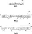
- FIG. 6 is a block diagram of an address 600 of a memory cell according to various embodiments of the invention.
- the address 600 is comprised of 32 bits [31:0] between a LSB 610 [0] and a MSB 620 [31].
- the address 600 includes row bits 630 [31:16] which are the highest order bits and then bank bits 640 [15:13].
- Ten column bits 650 are split into two groups [12:9] and [5:0], and three channel bits 660 [8:6] are located between the column bits 650 [12:9] and [5:0].
- the column bits 650 are therefore not contiguous.
- the channel bits 660 are of a higher order in the address 600 than the channel bits 460 in the address 400.
- the address 600 defines a 256 byte channel that is deeper than the 8 byte channel defined by the address 400.
- FIG. 7 is a block diagram of an address 700 of a memory cell according to various embodiments of the invention.
- the address 700 is comprised of 32 bits [31:0] between a LSB 710 [0] and a MSB 720 [31].
- the highest order bits in the address 700 are three channel bits 760 [31:29].
- the address 700 includes row bits 770 [28:13], bank bits 780 [12:10] and column bits 790 [9:0] in order.
- the channel bits 760 define a channel that is deeper than a bank of memory cells because the channel bits 760 are higher than the bank bits 780.
- the address 700 represents a divided memory system.
- the addresses 400, 600 and 700 each have multiple classes of address including a row address, a bank address, a column address and a channel address.
- the row address, the bank address and the column address have the same definition with respect to each other in all three addresses 400, 600 and 700.
- the definition of the channel address is different with respect to the other classes of address in each of the addresses 400, 600 and 700.
- the different definitions for the channel address result in a different depth of the channel for each of the addresses 400, 600 and 700.
- Changing the depth of the channel means a memory controller will access more or fewer bytes within a single channel before the address increments into the next channel. This has an impact on how data is stored in a memory system as illustrated in FIGs. 8 and 9 .
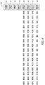
- FIG. 8 is a schematic diagram illustrating data received by the memory system 300 according to various embodiments of the invention.
- the memory system 300 is shown here to be receiving 64 bytes B[0] to B[63] addressed to shallow channels having a depth of 8 bytes with channel bits in the lowest order bits [n:0] of each address.
- the address 400 of FIG. 4 is an example of a shallow channel in which the three channel bits 460 [2:0] of the address 400 define an 8 byte channel.
- Each of the memory devices 310, 312, 314, 316, 318, 320, 322 and 324 has a pre-fetch of 8 bytes and receives bytes for a single channel during the execution of a memory request.
- the channel address increments every 8 bytes and the next channel in the next memory device will be accessed for each additional 8 bytes requested.
- the result is that 8 bytes B[0] to B[7] are written to the memory device 310, 8 bytes B[8] to B[15] are written to the memory device 312, and so on.
- 8 bytes are also written to each of the remaining memory devices 314, 316, 318, 320, 322 and 324. These accesses can occur in parallel or distributed in time across the channels.
- FIG. 9 is a schematic diagram illustrating data received by the memory system 300 according to various embodiments of the invention.
- the memory system 300 is shown to be receiving 64 bytes B[0] to B[63] addressed to channels having a depth of 16 bytes, deeper than the channels represented in FIG. 8 .
- Addresses for the data shown in FIG. 9 have channel bits [n:1], one bit higher than the channel bits of FIG. 8 .
- each of the memory devices 310, 312, 314, 316, 318, 320, 322 and 324 has a pre-fetch of 8 bytes and receives bytes for a single channel during the execution of a memory request.
- Each of the memory devices 310, 312 and 314 receives 16 bytes.
- the memory devices 318, 320, 322 and 324 receive no data.
- the result is that 64 bytes B[0] to B[63] are written to the memory devices 310, 312, 314 and 316.
- Each channel can be accessed concurrently or at different times to complete the request.
- the power usage and performance of a multi-channel memory system can be configured (e.g., scaled) by shifting the channel bits upwards.
- a shallow channel When a shallow channel is used, the number of memory devices accessed per memory request increases, potentially decreasing the access time for that memory request. However, the number of activations per memory request is higher for a shallow channel than it is for a deeper channel. For example, when the channel bits are assigned to bits [n:0] in the address 400 to create a shallow 8 byte channel as illustrated in FIG. 8 , a 64 byte memory request will access all eight memory devices 310, 312, 314, 316, 318, 320, 322 and 324 using all of the bandwidth of the memory system 300.
- the number of memory devices accessed per memory request decreases, potentially increasing the access time for that memory request.
- the number of activations per memory request is lower for a deeper channel than it is for a shallow channel. For example, if the channel bits are assigned to bits [n:1] in the address 400 to create a 16 byte channel as illustrated in FIG. 9 , a 64 byte memory request will activate only four memory devices 310, 312, 314 and 316, using one-half the available bandwidth of the memory system 300. In another example, the channel bits are assigned to bits [n:2] in the address 400 to create a 32 byte channel. A 64 byte memory request will access two memory devices 310 and 312 using one-fourth of the available bandwidth of the memory system 300.
- a channel depth for each region of a memory system is selected based on a desired balance between power usage and performance according to various embodiments of the invention.
- a channel depth for each region of the memory system 140 shown in FIG. 1 may be selected in the following manner.
- the first region 182 may serve, for example, a general processor that operates with a low latency response and a shallow channel depth.
- the shallow channel depth results in the use of all memory devices in a system to raise the bandwidth available per memory request.
- the first region 182 will supply more bandwidth for each memory request using more power than a region with deeper channels.
- the execution of a long memory request in shallow channels may result in the data looping around all of the channels more than once.
- the second region 184 may have deeper channels to serve, for example, a graphics processor that is more tolerant of latency.
- the second region 184 will supply less bandwidth per memory request, but will perform the memory request using less power because fewer rows of memory cells are accessed.
- a graphics processor is particularly suited for graphics applications.
- a memory system including thirteen memory devices may be operated in the following manner according to various embodiments of the invention.
- a channel X of the memory system is defined to include memory device 0 to memory device 7. Within the channel X, regions 0 through F are defined. Regions 0 - 3 are defined with a depth of 8 bytes. Regions 4 - 7 are defined with a depth of 32 bytes. Regions 8 - F are defined with a depth of 64 bytes.
- a channel Y is defined to include memory device 8 to memory device 11. Within the channel Y, regions 0 through 4 are defined. Regions 0 - 1 are defined with a depth of 64 bytes and regions 2 - 3 are defined with a depth of 128 bytes.
- a channel Z is defined as the only remaining memory device 13. The channel Z comprises only one memory device and does not have regional channel depth mapping. The power usage of each region and channel can be configured (e.g., controlled) separately for both active and inactive periods and the performance can vary from one channel to another.
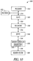
- FIG. 10 is a block diagram of a system 1000 according to various embodiments of the invention.
- a memory request is sent (e.g., transmitted) from a master such as a first processor 1010 over a first bus 1016 to a slave 1020.
- the system 1000 also includes a second processor 1022 that is coupled to the slave 1020 through the first bus 1016.
- the slave 1020 receives memory requests from multiple masters such as the processors 1010 and 1022 through the first bus 1016.
- the slave 1020 sends each memory request over a second bus 1024 to a pre-decode block 1030 that evaluates the memory request based on its size and address.
- the pre-decode block 1030 determines a region of the memory system 1060 to which the memory request is directed, and the depth of channels in the region.
- the pre-decode block 1030 rearranges the bits of the address in the memory request such that the memory request will be executed in the proper channels.
- the pre-decoder may compare the size of the memory request to the depth of the channels in the targeted region and generate sub-transactions.
- a sub-transaction can be the portion (e.g., "slice") of the initial request that will be written to or read from each channel.
- the pre-decode block 1030 then sends the memory request over a third bus 1036 to a queue 1040 where the memory request waits to be sent over a fourth bus 1044 to a memory controller 1050.
- the memory controller 1050 executes the memory request or sub-transaction in a memory system 1060 through a fifth bus 1066.
- the memory request or sub-transaction is executed according to a memory map 1070 in the memory controller 1050.
- the memory system 1060 may be the memory system 300 shown in FIG. 3 including the memory devices 310, 312, 314, 316, 318, 320, 322 and 324.
- the embodiments of the invention described herein are implemented by the pre-decode block 1030 and the memory controller 1050.
- the memory controller 1050 may execute the memory request by issuing simultaneous commands to some or all of the channels in the memory system 1060.
- the memory controller 1050 may compare the size of the memory request to the depth of each channel and the number of channels to determine the number of bytes to be communicated using each channel.
- Commands may be broadcast to multiple channels in the memory system 1060 during the same cycle if each channel has the same number of memory sub-transactions, such that multiple channels receive the same command. If the number of memory sub-transactions differ for the channels then two different commands may be issued to execute the memory request. A memory sub-transaction executes less than the entire memory request.
- the commands are issued with multiple chip select (CS) signals such that the correct memory devices in the memory system 1060 receive and execute the commands. Each channel responds to the memory controller 1050 when it receives a command.
- CS chip select
- FIG. 11 is a flow diagram of one method 1100 according to various embodiments of the invention.
- the method 1100 starts.
- a memory request including a request address is received from a master in a pre-decode block.
- the size of the memory request and the region of a memory system that the request address is directed to are determined.
- the depth of channels in the region of the memory system that the request address is directed to is determined.
- bits of the request address are rearranged into a first memory address according to a first definition if the request address corresponds to memory cells in a first region of the memory system.
- the bits of the request address are rearranged into a second memory address according to a second definition if the request address corresponds to memory cells in a second region of the memory system.
- the memory request is executed in a memory controller coupled between the pre-decode block and the memory system.
- the method 1100 ends.
- Various embodiments may have more or fewer activities than those shown in FIG. 11 . In some embodiments, the activities in FIG. 11 may be repeated, substituted for one another, and/or performed in serial or parallel fashion.
- FIG. 12 is a flow diagram of one method 1200 according to various embodiments of the invention.
- the method 1200 starts.
- memory cells are divided into a first region of memory cells and a second region of memory cells.
- a first address definition is selected according to which memory cells in the first region will be addressed.
- a second address definition is selected according to which memory cells in the second region will be addressed, the second address definition being different from the first address definition.
- the method 1200 ends.
- Various embodiments may have more or fewer activities than those shown in FIG. 12 . In some embodiments, the activities in FIGs. 11 and 12 may be repeated, substituted for one another, and/or performed in serial or parallel fashion.
- FIG. 13 is a block diagram of an address 1300 of a memory cell according to various embodiments of the invention.
- the address 1300 is comprised of 32 bits [31:0] between a LSB 1310 [0] and a MSB 1320 [31].
- the address 1300 includes row bits 1330 [31:16] which are the highest order bits including the MSB 1320.
- the address 1300 also includes bank bits 1340 [14:12], column bits 1350 [10:1] and three channel bits 1360 [15], [11] and [0].
- the row bits 1330, the bank bits 1340 and the column bits 1350 are separated from each other by a single channel bit 1360.
- the channel bits 1360 are distributed through the address 1300 and are not contiguous with each other.
- Memory systems that respond quickly and efficiently to memory requests are useful. Such systems may result by implementing various embodiments described herein, which may operate to include dividing a memory system into regions and accessing each region in a different manner, such as to allow the memory system to have some regions that operate with less power and other regions that respond to memory requests with low latency without using dedicated channels.
- the regions may be defined according to the type of data that will be stored therein. The relationship between power usage and latency can be varied across a single memory system.
- the size of each region is flexible and is not necessarily determined by the physical arrangement of the memory devices in the memory system.
- Memory systems and methods described herein according to various embodiments of the invention enable a varied granularity of memory cell groupings across different regions of a memory system. Neighboring regions of memory cells may have channels with different characteristics that are not based on the size of physical memory devices but rather on a desirable balance between power usage and performance. A memory request can be processed in a single channel or multiple channels to achieve the desired balance. Patterns of access to the memory system may thus depend on a configuration of the channels and a size of memory requests. A smaller memory request can be accomplished with fewer channels of memory cells to save power. Each memory request may be distributed across channels of memory cells based on the size of the memory request and a definition of the channels.
- 32 bits may be accessed in one of four 64 bit channels in a region having 256 bits in total rather than accessing all 256 bits at once.
- memory requests can be implemented to avoid reserving excessive numbers of memory cells.
- the proposed system can configure the access of memory cells based on the size of each request.
- the memory system may include a single memory device with multiple channels or multiple memory devices each having one or more channels. Accordingly, the specification and drawings are to be regarded in an illustrative rather than a restrictive sense.
Landscapes
- Engineering & Computer Science (AREA)
- Theoretical Computer Science (AREA)
- Physics & Mathematics (AREA)
- General Engineering & Computer Science (AREA)
- General Physics & Mathematics (AREA)
- Human Computer Interaction (AREA)
- Dram (AREA)
- Memory System (AREA)
- Static Random-Access Memory (AREA)
Abstract
Description
- This patent application claims priority benefit from
U.S. Application No. 13/042,164, filed 7 March 2011 , which is incorporated herein by reference in its entirety. - Memory systems are used in many devices such as personal digital assistants (PDAs), laptop computers, mobile phones and digital cameras. Some of these memory systems include multiple memory devices that receive memory requests from a single bus.
- Some embodiments are illustrated by way of example and not limitation in the figures of the accompanying drawings in which:
-
FIG. 1 is a block diagram of a system according to various embodiments of the invention; -
FIG. 2 is a block diagram of a system according to various embodiments of the invention; -
FIG. 3 is a block diagram of a memory system according to various embodiments of the invention; -
FIG. 4 is a block diagram of an address of a memory cell according to various embodiments of the invention; -
FIG. 5 is a block diagram of a programmable register according to various embodiments of the invention; -
FIG. 6 is a block diagram of an address of a memory cell according to various embodiments of the invention; -
FIG. 7 is a block diagram of an address of a memory cell according to various embodiments of the invention; -
FIG. 8 is a schematic diagram illustrating data received by a memory system according to various embodiments of the invention; -
FIG. 9 is a schematic diagram illustrating data received by the memory system according to various embodiments of the invention; -
FIG. 10 is a block diagram of a system according to various embodiments of the invention; -
FIG. 11 is a flow diagram of one method according to various embodiments of the invention; -
FIG. 12 is a flow diagram of one method according to various embodiments of the invention; and -
FIG. 13 is a block diagram of an address of a memory cell according to various embodiments of the invention. - Multi-channel memory systems have greater bandwidth and reduced power usage when compared to other systems. In some systems, each channel services a master or group of masters. This assignment allows for tighter quality of service control, but can reduce the bandwidth available from the memory system. When masters are dormant, the pins and bandwidth of the associated channels are idle and cannot be used by the rest of the system. The density of memory for each channel assigned to a master or group of masters may also be limited. For example, if a master only needs 128 kilobytes (KB) of memory, and the smallest available channel provides one gigabyte (GB) of memory, then a large portion of the channel will be unavailable because the entire channel is assigned to the master.
- The inventor has discovered that the challenges noted above, as well as others, can be addressed by operating a memory system with multiple regions of memory cells in which each region has, for example, its own channel definition. Regional channel definitions enable the power usage and performance of the memory system to be configured (e.g., tuned).
- In the following description, individual digits (e.g., binary digits, which are referred to hereinafter as "bits") are represented inside brackets. A single bit is represented as bit [G] where G is a non-negative integer from 0 upward. A group of consecutive bits is represented as bits [J:K] where J and K are non-negative integers. The consecutive bits in [J:K] begin with K and end with J. A byte has eight bits, and is represented by B[P] where P is a non-negative integer that identifies the byte.
-
FIG. 1 is a block diagram of asystem 100 according to various embodiments of the invention. Thesystem 100 includes afirst processor 110 coupled to abridge circuit 120 through afirst bus 130. Asecond processor 134 is also coupled to thebridge circuit 120 through thefirst bus 130. Thebridge circuit 120 is coupled to amemory system 140 through asecond bus 150. Thebridge circuit 120 executes memory requests from theprocessors memory controller 160, and transfers data between theprocessors memory system 140 over the first andsecond buses memory system 140 are located according to amemory map 170 in thememory controller 160. Memory cells in thememory system 140 may be divided (e.g., segmented) into multiple regions such as afirst region 182 and asecond region 184. Thememory system 140 may include, for example, one or more dynamic random access memory (DRAM) devices, synchronous dynamic random access memory (SDRAM) devices and Flash memory devices. Theprocessors system 100. -
FIG. 2 is a block diagram of asystem 200 according to various embodiments of the invention. Thesystem 200 includes a first processor, such as one included in a system-on-chip (SOC) 210, coupled to amemory system 240 through abus 250. A second processor, such as one included inSOC 256, is also coupled to thememory system 240 through thebus 250. TheSOCs system 200. The SOC 210 executes memory requests with a memory controller 260 that transfers data to and from thememory system 240 over thebus 250. Memory cells in thememory system 240 are located according to amemory map 270 in the memory controller 260. TheSOC 256 also includes amemory controller 280 and amemory map 282 to execute memory requests to thememory system 240. Memory cells in thememory system 240 may be divided into multiple regions such as afirst region 282 and asecond region 284. Thememory system 240 may include, for example, one or more DRAM devices, SDRAM devices and Flash memory devices. - Each
memory system FIGs. 1 and 2 may be a single memory device or multiple memory devices arranged to exchange data (e.g., information) through multiple pins coupled to a single bus such as thebus 150 or thebus 250.FIG. 3 is a block diagram of amemory system 300 according to various embodiments of the invention. Thememory system 300 comprises eightmemory devices memory devices data pins 340 to transfer data through the bus. Thememory devices FIG. 3 . There may be more or fewer than eight data pins in each of thememory devices - A memory map such as the
memory maps 170 and 270 (seeFIGs. 1 and 2 ) can be a structure of data that indicates how memory cells in thememory system 300 are oriented with respect to each other. A memory address received from a master is a collection of digits that may or may not correspond to (e.g., indicate or represent) the location of physical memory cells in thememory system 300. A memory map contains data to match the address from the master with one or more physical memory cells in thememory system 300. - A memory cell is accessed for read and write operations according to different classes of addresses, and each class of address has a definition. Addresses of a first class include a row address and a column address that, together, correspond to one memory cell at an intersection of a row and a column in an array of memory cells that has multiple rows and columns. The memory cells are divided into channels in multi-channel memory systems. A channel address is an address of a second class that identifies multiple memory cells in a channel in a multi-channel memory system. A bank address is an address of a third class that identifies a bank of multiple channels of memory cells. A system may have two or more banks of memory cells. The memory map discussed above also enables a division of the memory cells in a memory system into regions such as the
regions FIG. 1 and FIG. 2 . A region address is an address of a fourth class that identifies a region of memory cells in a multi-channel memory system as will be described herein below. -
FIG. 4 is a block diagram of anaddress 400 of a memory cell according to various embodiments of the invention. Theaddress 400 is comprised of 32 bits [31:0], each bit having a value of "0" or "1," the combination of bits used to indicate where the memory cell is to be found. The bits of theaddress 400 are arranged consecutively from left to right. Theaddress 400 has lower order bits toward the right, and the lowest order bit [0] is called a least significant bit (LSB) 410. Theaddress 400 has higher order bits toward the left, and the highest order bit [31] is called a most significant bit (MSB) 420. A lower order bit in theaddress 400 is closer to theLSB 410, and a higher order bit is closer to theMSB 420. Theaddress 400 includes row bits 430 [31:16] which are the highest order bits including theMSB 420. Next in theaddress 400 are bank bits 440 [15:13], column bits 450 [12:3] and channel bits 460 [2:0]. Thechannel bits 460 are the lowest order bits including theLSB 410. Theaddress 400 may comprise 30, 40, 42 or any number of bits other than 32 bits according to various embodiments of the invention. Different orders of bits than what is shown may also be used, including a reverse order. The number and location of therow bits 430, thebank bits 440, thecolumn bits 450 and thechannel bits 460 in theaddress 400 are the definition of theaddress 400. The definition can be changed by changing the number or location of these bits. The definition of theaddress 400 has an impact on how and where data is stored in a memory system. Each region can have a different address definition. - The
memory devices memory system 300 may operate as a multi-channel system, and the channels can be uniquely defined for each region. Such definitions, called regional channel definitions, allow all of the data pins 340 to be used per region or just a small subset of the data pins 340. Regional channel definitions enable different regions in a memory system to be configured (e.g., tailored) based on the type of data that will be stored in the region. For example, a region of a memory system that is used for graphics can have a deep channel definition that will save power with a reduced number of activations for each memory request when compared to a region with shallow channels. A deep channel will access more data per access before moving to the next channel than a shallow channel. The number of activations is the number of rows of memory cells that are accessed during execution of a memory request. Graphic masters may be relatively insensitive to latency, and an extra few nanoseconds for a memory request to execute will not substantially affect performance. - Regional channel definitions are implemented according to various embodiments of the invention by the
channel bits 460 in theaddress 400. Thechannel bits 460 may be located anywhere in theaddress 400, and may be contiguous or not contiguous with each other. - The regions may be implemented in at least two ways according to various embodiments of the invention. For example, bits of a region address may be added to the
address 400 to indicate a region of memory cells such as theregions FIG. 1 and FIG. 2 . The regions may also be defined by multiple programmable registers. -
FIG. 5 is a block diagram of aprogrammable register 500 according to various embodiments of the invention. An address associated with (e.g., in) a memory request ("a memory request address") from a master may be compared to a value in theprogrammable register 500 to determine which region of memory has the memory cell corresponding to the address. Theprogrammable register 500 includes sixteen bits to define a region, but more or fewer bits may be used. Each region of memory is defined by its own programmable register. The regions are not overlapping. Theprogrammable register 500 may be reprogrammed to change the definition of the regions during the life of a system. - Each region in a multi-channel memory system can have a different channel depth. The depth of a channel can be defined as the number of bytes that will be accessed from the channel before the address moves (e.g., rolls, increments, or crosses) into another channel. The depth of the channel can be determined by a prefetch of the memory device, and the location of the
channel bits 460 in theaddress 400. A prefetch is the smallest number of bits that can be received in the multi-channel memory system if it receives more than one bit at a time. The prefetch is determined by the memory device. If thechannel bits 460 are in the lowest order bits of theaddress 400 then the channel is shallow and a single memory request is more likely to span multiple channels. As thechannel bits 460 shift up to higher order bits in theaddress 400, the channel becomes deeper. More bytes can be accessed from a deeper channel before crossing to the next channel. For example, with respect to theaddress 400 shown inFIG. 4 , the three channel bits 460 [2:0] are the lowest order bits and define an 8 byte channel that is a shallow channel.FIG. 6 is a block diagram of an address 600 of a memory cell according to various embodiments of the invention. The address 600 is comprised of 32 bits [31:0] between a LSB 610 [0] and a MSB 620 [31]. The address 600 includes row bits 630 [31:16] which are the highest order bits and then bank bits 640 [15:13]. Tencolumn bits 650 are split into two groups [12:9] and [5:0], and three channel bits 660 [8:6] are located between the column bits 650 [12:9] and [5:0]. Thecolumn bits 650 are therefore not contiguous. When compared with theaddress 400 shown inFIG. 4 , thechannel bits 660 are of a higher order in the address 600 than thechannel bits 460 in theaddress 400. The address 600 defines a 256 byte channel that is deeper than the 8 byte channel defined by theaddress 400. -
FIG. 7 is a block diagram of anaddress 700 of a memory cell according to various embodiments of the invention. Theaddress 700 is comprised of 32 bits [31:0] between a LSB 710 [0] and a MSB 720 [31]. The highest order bits in theaddress 700 are three channel bits 760 [31:29]. Following thechannel bits 760, theaddress 700 includes row bits 770 [28:13], bank bits 780 [12:10] and column bits 790 [9:0] in order. Thechannel bits 760 define a channel that is deeper than a bank of memory cells because thechannel bits 760 are higher than thebank bits 780. Theaddress 700 represents a divided memory system. - The
addresses addresses addresses addresses - Changing the depth of the channel means a memory controller will access more or fewer bytes within a single channel before the address increments into the next channel. This has an impact on how data is stored in a memory system as illustrated in
FIGs. 8 and9 . -
FIG. 8 is a schematic diagram illustrating data received by thememory system 300 according to various embodiments of the invention. Thememory system 300 is shown here to be receiving 64 bytes B[0] to B[63] addressed to shallow channels having a depth of 8 bytes with channel bits in the lowest order bits [n:0] of each address. Theaddress 400 ofFIG. 4 is an example of a shallow channel in which the three channel bits 460 [2:0] of theaddress 400 define an 8 byte channel. Each of thememory devices memory device memory device 312, and so on. Thus, 8 bytes are also written to each of the remainingmemory devices - Data is stored in the memory system differently when the channels are deeper.
FIG. 9 is a schematic diagram illustrating data received by thememory system 300 according to various embodiments of the invention. In this case, thememory system 300 is shown to be receiving 64 bytes B[0] to B[63] addressed to channels having a depth of 16 bytes, deeper than the channels represented inFIG. 8 . Addresses for the data shown inFIG. 9 have channel bits [n:1], one bit higher than the channel bits ofFIG. 8 . As inFIG. 8 , each of thememory devices memory devices memory devices memory devices - Changing the depth of the channel has the most impact when the channel address bits are in lower order address bits in an address such as the
address 400 shown inFIG. 4 . The power usage and performance of a multi-channel memory system can be configured (e.g., scaled) by shifting the channel bits upwards. When a shallow channel is used, the number of memory devices accessed per memory request increases, potentially decreasing the access time for that memory request. However, the number of activations per memory request is higher for a shallow channel than it is for a deeper channel. For example, when the channel bits are assigned to bits [n:0] in theaddress 400 to create a shallow 8 byte channel as illustrated inFIG. 8 , a 64 byte memory request will access all eightmemory devices memory system 300. - When a deeper channel is used, the number of memory devices accessed per memory request decreases, potentially increasing the access time for that memory request. However, the number of activations per memory request is lower for a deeper channel than it is for a shallow channel. For example, if the channel bits are assigned to bits [n:1] in the
address 400 to create a 16 byte channel as illustrated inFIG. 9 , a 64 byte memory request will activate only fourmemory devices memory system 300. In another example, the channel bits are assigned to bits [n:2] in theaddress 400 to create a 32 byte channel. A 64 byte memory request will access twomemory devices memory system 300. - A channel depth for each region of a memory system is selected based on a desired balance between power usage and performance according to various embodiments of the invention. A channel depth for each region of the
memory system 140 shown inFIG. 1 may be selected in the following manner. Thefirst region 182 may serve, for example, a general processor that operates with a low latency response and a shallow channel depth. The shallow channel depth results in the use of all memory devices in a system to raise the bandwidth available per memory request. Thefirst region 182 will supply more bandwidth for each memory request using more power than a region with deeper channels. The execution of a long memory request in shallow channels may result in the data looping around all of the channels more than once. - The
second region 184 may have deeper channels to serve, for example, a graphics processor that is more tolerant of latency. Thesecond region 184 will supply less bandwidth per memory request, but will perform the memory request using less power because fewer rows of memory cells are accessed. A graphics processor is particularly suited for graphics applications. - In another example, a memory system including thirteen memory devices may be operated in the following manner according to various embodiments of the invention. A channel X of the memory system is defined to include
memory device 0 tomemory device 7. Within the channel X,regions 0 through F are defined. Regions 0 - 3 are defined with a depth of 8 bytes. Regions 4 - 7 are defined with a depth of 32 bytes. Regions 8 - F are defined with a depth of 64 bytes. A channel Y is defined to includememory device 8 tomemory device 11. Within the channel Y,regions 0 through 4 are defined. Regions 0 - 1 are defined with a depth of 64 bytes and regions 2 - 3 are defined with a depth of 128 bytes. A channel Z is defined as the only remainingmemory device 13. The channel Z comprises only one memory device and does not have regional channel depth mapping. The power usage of each region and channel can be configured (e.g., controlled) separately for both active and inactive periods and the performance can vary from one channel to another. -
FIG. 10 is a block diagram of a system 1000 according to various embodiments of the invention. A memory request is sent (e.g., transmitted) from a master such as afirst processor 1010 over afirst bus 1016 to aslave 1020. The system 1000 also includes asecond processor 1022 that is coupled to theslave 1020 through thefirst bus 1016. Theslave 1020 receives memory requests from multiple masters such as theprocessors first bus 1016. Theslave 1020 sends each memory request over asecond bus 1024 to apre-decode block 1030 that evaluates the memory request based on its size and address. Thepre-decode block 1030 determines a region of thememory system 1060 to which the memory request is directed, and the depth of channels in the region. Thepre-decode block 1030 rearranges the bits of the address in the memory request such that the memory request will be executed in the proper channels. The pre-decoder may compare the size of the memory request to the depth of the channels in the targeted region and generate sub-transactions. A sub-transaction can be the portion (e.g., "slice") of the initial request that will be written to or read from each channel. Thepre-decode block 1030 then sends the memory request over a third bus 1036 to aqueue 1040 where the memory request waits to be sent over afourth bus 1044 to amemory controller 1050. Thememory controller 1050 executes the memory request or sub-transaction in amemory system 1060 through afifth bus 1066. The memory request or sub-transaction is executed according to amemory map 1070 in thememory controller 1050. Thememory system 1060 may be thememory system 300 shown inFIG. 3 including thememory devices pre-decode block 1030 and thememory controller 1050. - The
memory controller 1050 may execute the memory request by issuing simultaneous commands to some or all of the channels in thememory system 1060. Thememory controller 1050 may compare the size of the memory request to the depth of each channel and the number of channels to determine the number of bytes to be communicated using each channel. Commands may be broadcast to multiple channels in thememory system 1060 during the same cycle if each channel has the same number of memory sub-transactions, such that multiple channels receive the same command. If the number of memory sub-transactions differ for the channels then two different commands may be issued to execute the memory request. A memory sub-transaction executes less than the entire memory request. The commands are issued with multiple chip select (CS) signals such that the correct memory devices in thememory system 1060 receive and execute the commands. Each channel responds to thememory controller 1050 when it receives a command. -
FIG. 11 is a flow diagram of onemethod 1100 according to various embodiments of the invention. Inblock 1110, themethod 1100 starts. Inblock 1120, a memory request including a request address is received from a master in a pre-decode block. Inblock 1130, the size of the memory request and the region of a memory system that the request address is directed to are determined. Inblock 1140, the depth of channels in the region of the memory system that the request address is directed to is determined. Inblock 1150, bits of the request address are rearranged into a first memory address according to a first definition if the request address corresponds to memory cells in a first region of the memory system. Inblock 1160, the bits of the request address are rearranged into a second memory address according to a second definition if the request address corresponds to memory cells in a second region of the memory system. Inblock 1170, the memory request is executed in a memory controller coupled between the pre-decode block and the memory system. Inblock 1180, themethod 1100 ends. Various embodiments may have more or fewer activities than those shown inFIG. 11 . In some embodiments, the activities inFIG. 11 may be repeated, substituted for one another, and/or performed in serial or parallel fashion. -
FIG. 12 is a flow diagram of onemethod 1200 according to various embodiments of the invention. Inblock 1210, themethod 1200 starts. Inblock 1220, memory cells are divided into a first region of memory cells and a second region of memory cells. Inblock 1230, a first address definition is selected according to which memory cells in the first region will be addressed. Inblock 1240, a second address definition is selected according to which memory cells in the second region will be addressed, the second address definition being different from the first address definition. Inblock 1250, themethod 1200 ends. Various embodiments may have more or fewer activities than those shown inFIG. 12 . In some embodiments, the activities inFIGs. 11 and12 may be repeated, substituted for one another, and/or performed in serial or parallel fashion. -
FIG. 13 is a block diagram of anaddress 1300 of a memory cell according to various embodiments of the invention. Theaddress 1300 is comprised of 32 bits [31:0] between a LSB 1310 [0] and a MSB 1320 [31]. Theaddress 1300 includes row bits 1330 [31:16] which are the highest order bits including theMSB 1320. Theaddress 1300 also includes bank bits 1340 [14:12], column bits 1350 [10:1] and three channel bits 1360 [15], [11] and [0]. Therow bits 1330, thebank bits 1340 and thecolumn bits 1350 are separated from each other by asingle channel bit 1360. Thechannel bits 1360 are distributed through theaddress 1300 and are not contiguous with each other. - Memory systems that respond quickly and efficiently to memory requests are useful. Such systems may result by implementing various embodiments described herein, which may operate to include dividing a memory system into regions and accessing each region in a different manner, such as to allow the memory system to have some regions that operate with less power and other regions that respond to memory requests with low latency without using dedicated channels. The regions may be defined according to the type of data that will be stored therein. The relationship between power usage and latency can be varied across a single memory system. The size of each region is flexible and is not necessarily determined by the physical arrangement of the memory devices in the memory system.
- Memory systems and methods described herein according to various embodiments of the invention enable a varied granularity of memory cell groupings across different regions of a memory system. Neighboring regions of memory cells may have channels with different characteristics that are not based on the size of physical memory devices but rather on a desirable balance between power usage and performance. A memory request can be processed in a single channel or multiple channels to achieve the desired balance. Patterns of access to the memory system may thus depend on a configuration of the channels and a size of memory requests. A smaller memory request can be accomplished with fewer channels of memory cells to save power. Each memory request may be distributed across channels of memory cells based on the size of the memory request and a definition of the channels. For example, 32 bits may be accessed in one of four 64 bit channels in a region having 256 bits in total rather than accessing all 256 bits at once. Thus, memory requests can be implemented to avoid reserving excessive numbers of memory cells. The proposed system can configure the access of memory cells based on the size of each request.
- Example structures and methods of managing a memory system have been described. Although specific embodiments have been described, it will be evident that various modifications and changes may be made to these embodiments. For example, the memory system may include a single memory device with multiple channels or multiple memory devices each having one or more channels. Accordingly, the specification and drawings are to be regarded in an illustrative rather than a restrictive sense.
- The Abstract of the Disclosure is provided to comply with 37 C.F.R. §1.72(b), requiring an abstract that allows the reader to quickly ascertain the nature of the technical disclosure. It is submitted with the understanding that it will not be used to interpret or limit the claims. In addition, in the foregoing Detailed Description, it may be seen that various features are grouped together in a single embodiment for the purpose of streamlining the disclosure. This method of disclosure is not to be interpreted as limiting the claims. Thus, the following claims are hereby incorporated into the Detailed Description, with each claim standing on its own as a separate embodiment.
Further embodiments are set out in the following clauses: - 1. A method of accessing memory cells, wherein the cells are divided into at least a first region and a second region, the method comprising:
- accessing a memory cell in the first region according to a first address definition; and
- accessing a memory cell in the second region according to a second address definition, the second address definition being different from the first address definition.
- 2. The method of
clause 1, wherein:- accessing the memory cell in the first region according to a first address definition comprises accessing the memory cell in the first region according to a first channel definition; and
- accessing the memory cell in the second region according to a second address definition comprises accessing the memory cell in the second region according to a second channel definition, the second channel definition being different from the first channel definition.
- 3. The method of
clause 1, further comprising reading a region digit in a memory request address to determine which of the regions has the memory cells corresponding to the memory request address. - 4. The method of
clause 1, further comprising comparing a memory request address to a value in a register to determine which of the regions has the memory cell corresponding to the memory request address. - 5. The method of
clause 4, further comprising reprogramming the register to change one of the definitions. - 6. The method of
clause 1, further comprising:- comparing a memory request address to a value in a first register to determine whether the first region has the memory cell corresponding to the memory request address; and
- comparing the memory request address to a value in a second register to determine whether the second region has the memory cell corresponding to the memory request address.
- 7. A method comprising;
receiving a memory request; and
distributing the memory request across a plurality of channels of memory cells based on a size of the memory request and a definition of the channels. - 8. A method comprising:
- accessing memory cells in a first region of a memory system with all of a plurality of classes of address, wherein a selected one of the classes of address has a first address definition; and
- accessing memory cells in a second region of the memory system with all of the classes of address, wherein the selected class of address has a second address definition that is different from the first address definition.
- 9. The method of
clause 8, wherein the classes of address comprise a row address, a column address, a channel address and a bank address. - 10. The method of
clause 9, wherein the classes of address further comprise a region address. - 11. The method of
clause 8, wherein accessing memory cells in a second region further comprises accessing memory cells in the second region with an address including channel address digits that are of a higher order than channel address digits in an address used to access memory cells in the first region. - 12. The method of
clause 8, wherein accessing memory cells in a second region further comprises accessing memory cells in the second region with channel address digits that are not contiguous in an address. - 13. The method of
clause 8, wherein the selected class of address comprises a channel address. - 14. A method comprising:
- accessing data in a first region of memory cells of a memory system, wherein the memory cells of the memory system are divided into channels, each channel comprising a plurality of memory cells; and
- accessing data in a second region of memory cells of the memory system wherein a number of bytes accessed per channel before going to a next channel in the first region is different than a number of bytes accessed per channel before going to a next channel in the second region.
- 15. The method of
clause 14, wherein accessing data in the second region of memory cells further comprises accessing the data in the second region of memory cells with less power than is used to access data in the first region of memory cells. - 16. The method of
clause 14, wherein accessing data in the second region of memory cells further comprises accessing the data in the second region of memory cells with a greater latency than is used to access data in the first region of memory cells. - 17. The method of
clause 14, wherein accessing data in the second region of memory cells further comprises broadcasting commands to at least some of the channels in the second region of memory cells. - 18. A method comprising:
- receiving data in a memory request from a master;
- writing the data to a first region of memory cells of a memory system if the master is of a first type; and
- writing the data to a second region of memory cells of the memory system if the master is of a second type.
- 19. The method of
clause 18, wherein:- writing the data to a first region further comprises writing the data to the first region of memory cells of the memory system if the master operates to tolerate a selected amount of latency; and
- writing the data to a second region further comprises writing the data to the second region of memory cells of the memory system if the master does not tolerate the selected amount of latency.
- 20. The method of
clause 18, wherein:- writing the data to a first region further comprises writing the data to the first region of memory cells of the memory system if the master comprises a general processor; and
- writing the data to a second region further comprises writing the data to the second region of memory cells of the memory system if the master comprises a graphics processor.
- 21. The method of
clause 18, wherein:- writing the data to a first region further comprises writing the data to all memory devices in the first region; and
- writing the data to a second region further comprises writing the data to less than all memory devices in the second region.
- 22. A system comprising:
- a pre-decode block to:
- receive a request address associated with a memory request corresponding to memory cells in a memory system;
- rearrange the request address into a first memory address according to a first definition if the request address corresponds to memory cells in a first region of the memory system; and
- rearrange the request address into a second memory address according to a second definition if the request address corresponds to memory cells in a second region of the memory system, the second definition being different from the first definition; and
- a memory controller configured to receive the first or the second memory address and to execute at least a portion of the memory request in the memory system.
- a pre-decode block to:
- 23. The system of
clause 22, wherein the memory system comprises a plurality of memory devices including data pins coupled to a bus to transfer data through the bus. - 24. The system of
clause 22, wherein the memory devices comprise dynamic random access memory (DRAM) devices, synchronous dynamic random access memory (SDRAM) devices, and/or Flash memory devices in any combination. - 25. The system of
clause 22, wherein the pre-decode block is coupled to a plurality of masters through a bus to receive memory requests from the masters. - 26. The system of
clause 25, wherein a first one of the masters comprises a general processor. - 27. The system of
clause 25, wherein a second one of the masters comprises a graphics processor. - 28. A method comprising:
- receiving a request address associated with a memory request from a master in a pre-decode block;
- determining a region of a memory system to which the request address is directed;
- rearranging digits of the request address into a first memory address according to a first definition if the request address corresponds to memory cells in a first region of the memory system; and
- rearranging the digits of the request address into a second memory address according to a second definition if the request address corresponds to memory cells in a second region of the memory system, the second definition being different from the first definition.
- 29. The method of
clause 28, further comprising comparing a size of the memory request to a depth of the region to which the request address is directed. - 30. The method of
clause 29, further comprising generating sub-transactions, each sub-transaction being a portion of the memory request to be written to or read from the region. - 31. The method of
clause 28, further comprising determining a depth of channels in the region of the memory system to which the request address is directed. - 32. The method of
clause 28, wherein channels in the second region of the memory system comprise more bytes than channels in the first region of the memory system. - 33. The method of
clause 28, further comprising executing at least a portion of the memory request in a memory controller coupled between the pre-decode block and the memory system. - 34. A system comprising a plurality of memory cells divided into at least first and second regions, wherein an address definition of the first region is different than an address definition of the second region.
- 35. The system of
clause 34, wherein each of the regions is configured with respect to a type of access that will occur in the respective region. - 36. The system of
clause 35, wherein the type of access that will occur in the respective region is based on a type of data stored in the respective region. - 37. The system of
clause 34, wherein each of the regions is configured based on a type of data to be stored in the respective region. - 38. The system of
clause 34, further comprising at least first and second registers, wherein the first register defines the first region and the second register defines the second region. - 39. The system of
clause 34, wherein the address definitions are channel address definitions. - 40. The system of
clause 34, wherein the first region has a different channel depth than the second region. - 41. A memory controller configured to execute memory requests in a memory system, wherein the memory controller includes a memory map that divides memory cells in the memory system into a plurality of regions, wherein each of the regions has its own address definition.
Claims (12)
- A method of accessing memory cells, wherein the cells are divided into at least a first region and a second region, the method comprising:accessing at least a first memory cell in the first region according to a first address definition, the first address definition including multiple bits identifying each of the bank, row, column, and channel depth for at least the first memory cell to be accessed in the first region, the first region having a first channel depth; andaccessing at least a second memory cell in the second region according to a second address definition, the second address definition including multiple bits identifying each of the bank, row, column, and channel depth for at least the second memory cell to be accessed in the second region, the second region having a second channel depth different from the first channel depth of the first region.
- The method of claim 1, further comprising:receiving a memory request address; andreading a region digit in the memory request address to determine which of the regions has the at least one memory cell corresponding to the memory request address.
- The method of claim 1, further comprising:receiving a memory request address; andcomparing the memory request address to a value in a register to determine which of the regions has the at least one memory cell corresponding to the memory request address.
- The method of claim 3, further comprising reprogramming the register to change one of the address definitions.
- The method of claim 1, further comprising:comparing a received memory request address to a value in a first register to determine whether the first region has the memory cell corresponding to the memory request address; andwhen the memory cell corresponding to the received memory request is not found to be in the first region, comparing the received memory request address to a value in a second register to determine whether the second region has the memory cell corresponding to the memory request address.
- The method of any of claims 1-5, wherein accessing at least the second memory cell in the second region according to a second address definition further comprises accessing at least the second memory cell with an address including channel address digits that are of a higher order than channel address digits in an address used to access at least the first memory cell in the first region.
- The method of any of claims 1-6, further comprising:receiving first and second memory request addresses originating from first and second masters, respectively, each memory request address including data to be written to the memory system;in response to the first memory request address, writing the data to the first region of memory cells, wherein writing the data to the first region comprises writing the data to all memory devices in the first region; andin response to the second memory request address, writing the data to the second region of memory cells of the memory system, wherein writing the data to the second region comprises writing the data to less than all memory devices in the second region.
- A system, comprising:a first processor;a second processor;a memory system coupled to each of the first and second processors, the memory system comprising multiple memory cells divided into at least first and second regions, the first region having a first channel depth, and the second region having a second channel depth, different from the first channel depth, wherein the channel depth is the number of bytes that will be accessed from the channel before the address moves to another channel;a pre-decoder configured to process memory requests generated by the first and second processors in reference to the memory request size and address, including,determining the region of the memory system to which each memory request is directed and the depth of one or more channels in the region,for memory request addresses corresponding to memory cells in the first region of the memory system, rearranging the bits of the address into a first memory address according to a first definition, the first address definition including multiple bits identifying each of the bank, row, column, and channel depth of at least the first memory cell to be accessed in the first region, andfor memory request addresses corresponding to memory cells in the second region of the memory system, rearranging the bits of the address into a second memory address according to a second definition, the second address definition including multiple bits identifying each of the bank, row, column, and channel depth of at least the second memory cell to be accessed in the second region.
- The system of claim 8, wherein the pre-decoder is further configured to rearrange the bits of the address into the second memory address according to a second definition with an address including channel address digits that are of a higher order than channel address digits in an address used to access at least the first memory cell in the first region.
- The system of any of claims 8-9, wherein:data is written to the first region if the first processor is of a first type that does not tolerate a selected amount of latency; anddata is written to the second region if the second processor is of a second type that operates to tolerate a selected amount of latency.
- The system of claim 10, wherein the first processor comprises a general processor.
- The system of any of claims 10-11, wherein the second processor comprises a graphics processor.
Applications Claiming Priority (3)
| Application Number | Priority Date | Filing Date | Title |
|---|---|---|---|
| US13/042,164 US8892844B2 (en) | 2011-03-07 | 2011-03-07 | Methods of accessing memory cells, methods of distributing memory requests, systems, and memory controllers |
| PCT/US2012/027905 WO2012122182A2 (en) | 2011-03-07 | 2012-03-06 | Methods of accessing memory cells, methods of distributing memory requests, systems, and memory controllers |
| EP12755210.7A EP2684133B1 (en) | 2011-03-07 | 2012-03-06 | Methods of accessing memory cells, methods of distributing memory requests, systems, and memory controllers |
Related Parent Applications (1)
| Application Number | Title | Priority Date | Filing Date |
|---|---|---|---|
| EP12755210.7A Division EP2684133B1 (en) | 2011-03-07 | 2012-03-06 | Methods of accessing memory cells, methods of distributing memory requests, systems, and memory controllers |
Publications (2)
| Publication Number | Publication Date |
|---|---|
| EP3373150A1 true EP3373150A1 (en) | 2018-09-12 |
| EP3373150B1 EP3373150B1 (en) | 2020-05-13 |
Family
ID=46797130
Family Applications (2)
| Application Number | Title | Priority Date | Filing Date |
|---|---|---|---|
| EP12755210.7A Active EP2684133B1 (en) | 2011-03-07 | 2012-03-06 | Methods of accessing memory cells, methods of distributing memory requests, systems, and memory controllers |
| EP18170452.9A Active EP3373150B1 (en) | 2011-03-07 | 2012-03-06 | Methods of accessing memory cells, methods of distributing memory requests, systems, and memory controllers |
Family Applications Before (1)
| Application Number | Title | Priority Date | Filing Date |
|---|---|---|---|
| EP12755210.7A Active EP2684133B1 (en) | 2011-03-07 | 2012-03-06 | Methods of accessing memory cells, methods of distributing memory requests, systems, and memory controllers |
Country Status (6)
| Country | Link |
|---|---|
| US (3) | US8892844B2 (en) |
| EP (2) | EP2684133B1 (en) |
| KR (1) | KR101993651B1 (en) |
| CN (2) | CN103493026B (en) |
| TW (1) | TWI539286B (en) |
| WO (1) | WO2012122182A2 (en) |
Families Citing this family (11)
| Publication number | Priority date | Publication date | Assignee | Title |
|---|---|---|---|---|
| US8892844B2 (en) | 2011-03-07 | 2014-11-18 | Micron Technology, Inc. | Methods of accessing memory cells, methods of distributing memory requests, systems, and memory controllers |
| US10838886B2 (en) | 2011-04-19 | 2020-11-17 | Micron Technology, Inc. | Channel depth adjustment in memory systems |
| US9208755B2 (en) | 2012-12-03 | 2015-12-08 | Nvidia Corporation | Low power application execution on a data processing device having low graphics engine utilization |
| US9183057B2 (en) | 2013-01-21 | 2015-11-10 | Micron Technology, Inc. | Systems and methods for accessing memory |
| US10042750B2 (en) * | 2013-03-15 | 2018-08-07 | Micron Technology, Inc. | Apparatuses and methods for adaptive control of memory using an adaptive memory controller with a memory management hypervisor |
| US9507628B1 (en) * | 2015-09-28 | 2016-11-29 | International Business Machines Corporation | Memory access request for a memory protocol |
| KR102530889B1 (en) * | 2016-04-06 | 2023-05-11 | 에스케이하이닉스 주식회사 | Data processing system and operating method of data processing system |
| KR102760721B1 (en) | 2016-11-30 | 2025-02-03 | 삼성전자주식회사 | Storage device supporting byte accessible interface and block accessible interface and electronic system including the same |
| US10977198B2 (en) | 2018-09-12 | 2021-04-13 | Micron Technology, Inc. | Hybrid memory system interface |
| US11960735B2 (en) * | 2021-09-01 | 2024-04-16 | Micron Technology, Inc. | Memory channel controller operation based on data types |
| KR20240063607A (en) * | 2022-11-03 | 2024-05-10 | 삼성전자주식회사 | Swap memory device providing data and data block, method of operating the same, and method of operating electronic device including the same |
Citations (3)
| Publication number | Priority date | Publication date | Assignee | Title |
|---|---|---|---|---|
| EP0777233A1 (en) * | 1995-11-30 | 1997-06-04 | Cirrus Logic, Inc. | A memory architecture using conserved adressing and systems and methods using the same |
| US6470409B1 (en) * | 1996-11-26 | 2002-10-22 | Xilinx Inc. | Interface system having a programmable number of channels and methods of implementing same |
| US6816165B1 (en) * | 2000-12-13 | 2004-11-09 | Micron Technology, Inc. | Memory system having multiple address allocation formats and method for use thereof |
Family Cites Families (28)
| Publication number | Priority date | Publication date | Assignee | Title |
|---|---|---|---|---|
| US5465332A (en) * | 1992-09-21 | 1995-11-07 | International Business Machines Corporation | Selectable 8/16 bit DMA channels for "ISA" bus |
| JPH06332664A (en) | 1993-03-23 | 1994-12-02 | Toshiba Corp | Display control system |
| JPH08278916A (en) | 1994-11-30 | 1996-10-22 | Hitachi Ltd | Multi-channel memory system, transfer information synchronization method and signal transfer circuit |
| US5787445A (en) | 1996-03-07 | 1998-07-28 | Norris Communications Corporation | Operating system including improved file management for use in devices utilizing flash memory as main memory |
| JPH09259041A (en) | 1996-03-27 | 1997-10-03 | Hitachi Ltd | Cache memory control method |
| JPH10232819A (en) | 1997-02-20 | 1998-09-02 | Canon Inc | Memory control device and memory access method |
| US5956743A (en) | 1997-08-25 | 1999-09-21 | Bit Microsystems, Inc. | Transparent management at host interface of flash-memory overhead-bytes using flash-specific DMA having programmable processor-interrupt of high-level operations |
| JP3546788B2 (en) * | 1999-12-20 | 2004-07-28 | 日本電気株式会社 | Memory control circuit |
| WO2003085677A1 (en) | 2002-04-05 | 2003-10-16 | Renesas Technology Corp. | Nonvolatile storage device |
| AU2003271629A1 (en) * | 2002-09-30 | 2004-04-19 | Telefonaktiebolaget Lm Ericsson (Publ) | Method and memory controller for scalable multi-channel memory access |
| US7093047B2 (en) | 2003-07-03 | 2006-08-15 | Integrated Device Technology, Inc. | Integrated circuit memory devices having clock signal arbitration circuits therein and methods of performing clock signal arbitration |
| TWI299497B (en) | 2004-06-24 | 2008-08-01 | Via Tech Inc | Method and related apparatus for accessing memory apparatus |
| JP3955862B2 (en) | 2004-09-27 | 2007-08-08 | 株式会社ルネサステクノロジ | Data processing apparatus and system using the same |
| US7394288B1 (en) | 2004-12-13 | 2008-07-01 | Massachusetts Institute Of Technology | Transferring data in a parallel processing environment |
| US7480761B2 (en) * | 2005-01-10 | 2009-01-20 | Microsoft Corporation | System and methods for an overlay disk and cache using portable flash memory |
| US7765366B2 (en) * | 2005-06-23 | 2010-07-27 | Intel Corporation | Memory micro-tiling |
| US7502908B2 (en) * | 2006-05-04 | 2009-03-10 | International Business Machines Corporation | Method for providing an address format compatible with different addressing formats used for addressing different sized address spaces |
| US7797319B2 (en) | 2006-05-15 | 2010-09-14 | Algebraix Data Corporation | Systems and methods for data model mapping |
| US7525842B2 (en) | 2007-01-25 | 2009-04-28 | Micron Technology, Inc. | Increased NAND flash memory read throughput |
| US9495290B2 (en) | 2007-06-25 | 2016-11-15 | Sonics, Inc. | Various methods and apparatus to support outstanding requests to multiple targets while maintaining transaction ordering |
| JP2009053675A (en) | 2007-07-30 | 2009-03-12 | Nippon Synthetic Chem Ind Co Ltd:The | Adhesive for polarizing plate, polarizing plate, and production method thereof |
| JP5731730B2 (en) * | 2008-01-11 | 2015-06-10 | ピーエスフォー ルクスコ エスエイアールエルPS4 Luxco S.a.r.l. | Semiconductor memory device and data processing system including the semiconductor memory device |
| KR100948158B1 (en) | 2008-06-16 | 2010-03-18 | 엘지전자 주식회사 | Multi processor including a graphics core, a computer having the same and a memory operating method thereof |
| US8386750B2 (en) * | 2008-10-31 | 2013-02-26 | Cray Inc. | Multiprocessor system having processors with different address widths and method for operating the same |
| US7859932B2 (en) | 2008-12-18 | 2010-12-28 | Sandisk Corporation | Data refresh for non-volatile storage |
| US8018752B2 (en) | 2009-03-23 | 2011-09-13 | Micron Technology, Inc. | Configurable bandwidth memory devices and methods |
| CN101702326B (en) * | 2009-10-30 | 2012-08-29 | 曙光信息产业(北京)有限公司 | Memory controller |
| US8892844B2 (en) | 2011-03-07 | 2014-11-18 | Micron Technology, Inc. | Methods of accessing memory cells, methods of distributing memory requests, systems, and memory controllers |
-
2011
- 2011-03-07 US US13/042,164 patent/US8892844B2/en active Active
-
2012
- 2012-03-06 EP EP12755210.7A patent/EP2684133B1/en active Active
- 2012-03-06 WO PCT/US2012/027905 patent/WO2012122182A2/en not_active Ceased
- 2012-03-06 CN CN201280019658.6A patent/CN103493026B/en active Active
- 2012-03-06 EP EP18170452.9A patent/EP3373150B1/en active Active
- 2012-03-06 KR KR1020137025982A patent/KR101993651B1/en active Active
- 2012-03-06 CN CN201710050923.1A patent/CN107025181B/en active Active
- 2012-03-07 TW TW101107727A patent/TWI539286B/en active
-
2014
- 2014-11-17 US US14/542,750 patent/US9933972B2/en active Active
-
2018
- 2018-03-12 US US15/918,178 patent/US10162557B2/en active Active
Patent Citations (3)
| Publication number | Priority date | Publication date | Assignee | Title |
|---|---|---|---|---|
| EP0777233A1 (en) * | 1995-11-30 | 1997-06-04 | Cirrus Logic, Inc. | A memory architecture using conserved adressing and systems and methods using the same |
| US6470409B1 (en) * | 1996-11-26 | 2002-10-22 | Xilinx Inc. | Interface system having a programmable number of channels and methods of implementing same |
| US6816165B1 (en) * | 2000-12-13 | 2004-11-09 | Micron Technology, Inc. | Memory system having multiple address allocation formats and method for use thereof |
Also Published As
| Publication number | Publication date |
|---|---|
| EP2684133A4 (en) | 2015-05-06 |
| US9933972B2 (en) | 2018-04-03 |
| WO2012122182A3 (en) | 2013-01-31 |
| KR20140013010A (en) | 2014-02-04 |
| EP2684133A2 (en) | 2014-01-15 |
| CN107025181B (en) | 2020-07-31 |
| US10162557B2 (en) | 2018-12-25 |
| WO2012122182A2 (en) | 2012-09-13 |
| US8892844B2 (en) | 2014-11-18 |
| KR101993651B1 (en) | 2019-06-27 |
| US20180300079A1 (en) | 2018-10-18 |
| CN103493026B (en) | 2017-02-15 |
| TW201243606A (en) | 2012-11-01 |
| US20120233413A1 (en) | 2012-09-13 |
| CN103493026A (en) | 2014-01-01 |
| TWI539286B (en) | 2016-06-21 |
| US20150074370A1 (en) | 2015-03-12 |
| EP3373150B1 (en) | 2020-05-13 |
| CN107025181A (en) | 2017-08-08 |
| EP2684133B1 (en) | 2018-05-23 |
Similar Documents
| Publication | Publication Date | Title |
|---|---|---|
| US10162557B2 (en) | Methods of accessing memory cells, methods of distributing memory requests, systems, and memory controllers | |
| JP7818579B2 (en) | A hardware-software cooperative address mapping scheme for efficient processing-in-memory | |
| CN108874303B (en) | Storage system and method for non-volatile memory command collision avoidance | |
| CN111095418A (en) | Method and apparatus for specifying read voltage offset for read command | |
| CN114185818A (en) | GPU memory access adaptive optimization method and device based on extended page table | |
| EP3716076B1 (en) | Technologies for providing high efficiency compute architecture on cross point memory for artificial intelligence operations | |
| EP3739457B1 (en) | Technologies for performing macro operations in memory | |
| WO2017151262A1 (en) | Method and apparatus for providing a contiguously addressable memory region by remapping an address space | |
| CN118525335B (en) | Method and apparatus for recovering conventional access performance in fine-grained DRAM | |
| US20200379546A1 (en) | Dynamic power management network for memory devices | |
| US11640444B2 (en) | Device and method for accelerating matrix multiply operations | |
| RU2481652C1 (en) | Integrated circuit with multi-port super memory cell and circuit of data transfer route switching | |
| WO2021026095A1 (en) | Memory controller for non-interfering accesses to nonvolatile memory by different masters, and related systems and methods | |
| US20240385974A1 (en) | Multiple precision memory system | |
| CN103477330A (en) | Channel depth adjustment in memory systems | |
| KR20220123597A (en) | Memory cell level assignment using optimal level permutations in a non-volatile memory | |
| US12158842B2 (en) | Data co-location using address hashing for high-performance processing in memory | |
| US20250208793A1 (en) | Data writing method, storage device, and computer-readable storage device | |
| CN113223565A (en) | Configurable control of integrated circuits |
Legal Events
| Date | Code | Title | Description |
|---|---|---|---|
| PUAI | Public reference made under article 153(3) epc to a published international application that has entered the european phase |
Free format text: ORIGINAL CODE: 0009012 |
|
| STAA | Information on the status of an ep patent application or granted ep patent |
Free format text: STATUS: REQUEST FOR EXAMINATION WAS MADE |
|
| 17P | Request for examination filed |
Effective date: 20180502 |
|
| AC | Divisional application: reference to earlier application |
Ref document number: 2684133 Country of ref document: EP Kind code of ref document: P |
|
| AK | Designated contracting states |
Kind code of ref document: A1 Designated state(s): AL AT BE BG CH CY CZ DE DK EE ES FI FR GB GR HR HU IE IS IT LI LT LU LV MC MK MT NL NO PL PT RO RS SE SI SK SM TR |
|
| GRAP | Despatch of communication of intention to grant a patent |
Free format text: ORIGINAL CODE: EPIDOSNIGR1 |
|
| STAA | Information on the status of an ep patent application or granted ep patent |
Free format text: STATUS: GRANT OF PATENT IS INTENDED |
|
| INTG | Intention to grant announced |
Effective date: 20191014 |
|
| GRAS | Grant fee paid |
Free format text: ORIGINAL CODE: EPIDOSNIGR3 |
|
| GRAA | (expected) grant |
Free format text: ORIGINAL CODE: 0009210 |
|
| STAA | Information on the status of an ep patent application or granted ep patent |
Free format text: STATUS: THE PATENT HAS BEEN GRANTED |
|
| AC | Divisional application: reference to earlier application |
Ref document number: 2684133 Country of ref document: EP Kind code of ref document: P |
|
| AK | Designated contracting states |
Kind code of ref document: B1 Designated state(s): AL AT BE BG CH CY CZ DE DK EE ES FI FR GB GR HR HU IE IS IT LI LT LU LV MC MK MT NL NO PL PT RO RS SE SI SK SM TR |
|
| REG | Reference to a national code |
Ref country code: GB Ref legal event code: FG4D |
|
| REG | Reference to a national code |
Ref country code: CH Ref legal event code: EP |
|
| REG | Reference to a national code |
Ref country code: DE Ref legal event code: R096 Ref document number: 602012070162 Country of ref document: DE |
|
| REG | Reference to a national code |
Ref country code: AT Ref legal event code: REF Ref document number: 1271163 Country of ref document: AT Kind code of ref document: T Effective date: 20200615 |
|
| REG | Reference to a national code |
Ref country code: LT Ref legal event code: MG4D |
|
| REG | Reference to a national code |
Ref country code: NL Ref legal event code: MP Effective date: 20200513 |
|
| PG25 | Lapsed in a contracting state [announced via postgrant information from national office to epo] |
Ref country code: SE Free format text: LAPSE BECAUSE OF FAILURE TO SUBMIT A TRANSLATION OF THE DESCRIPTION OR TO PAY THE FEE WITHIN THE PRESCRIBED TIME-LIMIT Effective date: 20200513 Ref country code: IS Free format text: LAPSE BECAUSE OF FAILURE TO SUBMIT A TRANSLATION OF THE DESCRIPTION OR TO PAY THE FEE WITHIN THE PRESCRIBED TIME-LIMIT Effective date: 20200913 Ref country code: PT Free format text: LAPSE BECAUSE OF FAILURE TO SUBMIT A TRANSLATION OF THE DESCRIPTION OR TO PAY THE FEE WITHIN THE PRESCRIBED TIME-LIMIT Effective date: 20200914 Ref country code: FI Free format text: LAPSE BECAUSE OF FAILURE TO SUBMIT A TRANSLATION OF THE DESCRIPTION OR TO PAY THE FEE WITHIN THE PRESCRIBED TIME-LIMIT Effective date: 20200513 Ref country code: NO Free format text: LAPSE BECAUSE OF FAILURE TO SUBMIT A TRANSLATION OF THE DESCRIPTION OR TO PAY THE FEE WITHIN THE PRESCRIBED TIME-LIMIT Effective date: 20200813 Ref country code: GR Free format text: LAPSE BECAUSE OF FAILURE TO SUBMIT A TRANSLATION OF THE DESCRIPTION OR TO PAY THE FEE WITHIN THE PRESCRIBED TIME-LIMIT Effective date: 20200814 Ref country code: LT Free format text: LAPSE BECAUSE OF FAILURE TO SUBMIT A TRANSLATION OF THE DESCRIPTION OR TO PAY THE FEE WITHIN THE PRESCRIBED TIME-LIMIT Effective date: 20200513 |
|
| PG25 | Lapsed in a contracting state [announced via postgrant information from national office to epo] |
Ref country code: BG Free format text: LAPSE BECAUSE OF FAILURE TO SUBMIT A TRANSLATION OF THE DESCRIPTION OR TO PAY THE FEE WITHIN THE PRESCRIBED TIME-LIMIT Effective date: 20200813 Ref country code: RS Free format text: LAPSE BECAUSE OF FAILURE TO SUBMIT A TRANSLATION OF THE DESCRIPTION OR TO PAY THE FEE WITHIN THE PRESCRIBED TIME-LIMIT Effective date: 20200513 Ref country code: HR Free format text: LAPSE BECAUSE OF FAILURE TO SUBMIT A TRANSLATION OF THE DESCRIPTION OR TO PAY THE FEE WITHIN THE PRESCRIBED TIME-LIMIT Effective date: 20200513 Ref country code: LV Free format text: LAPSE BECAUSE OF FAILURE TO SUBMIT A TRANSLATION OF THE DESCRIPTION OR TO PAY THE FEE WITHIN THE PRESCRIBED TIME-LIMIT Effective date: 20200513 |
|
| REG | Reference to a national code |
Ref country code: AT Ref legal event code: MK05 Ref document number: 1271163 Country of ref document: AT Kind code of ref document: T Effective date: 20200513 |
|
| PG25 | Lapsed in a contracting state [announced via postgrant information from national office to epo] |
Ref country code: AL Free format text: LAPSE BECAUSE OF FAILURE TO SUBMIT A TRANSLATION OF THE DESCRIPTION OR TO PAY THE FEE WITHIN THE PRESCRIBED TIME-LIMIT Effective date: 20200513 Ref country code: NL Free format text: LAPSE BECAUSE OF FAILURE TO SUBMIT A TRANSLATION OF THE DESCRIPTION OR TO PAY THE FEE WITHIN THE PRESCRIBED TIME-LIMIT Effective date: 20200513 |
|
| PG25 | Lapsed in a contracting state [announced via postgrant information from national office to epo] |
Ref country code: SM Free format text: LAPSE BECAUSE OF FAILURE TO SUBMIT A TRANSLATION OF THE DESCRIPTION OR TO PAY THE FEE WITHIN THE PRESCRIBED TIME-LIMIT Effective date: 20200513 Ref country code: EE Free format text: LAPSE BECAUSE OF FAILURE TO SUBMIT A TRANSLATION OF THE DESCRIPTION OR TO PAY THE FEE WITHIN THE PRESCRIBED TIME-LIMIT Effective date: 20200513 Ref country code: IT Free format text: LAPSE BECAUSE OF FAILURE TO SUBMIT A TRANSLATION OF THE DESCRIPTION OR TO PAY THE FEE WITHIN THE PRESCRIBED TIME-LIMIT Effective date: 20200513 Ref country code: AT Free format text: LAPSE BECAUSE OF FAILURE TO SUBMIT A TRANSLATION OF THE DESCRIPTION OR TO PAY THE FEE WITHIN THE PRESCRIBED TIME-LIMIT Effective date: 20200513 Ref country code: DK Free format text: LAPSE BECAUSE OF FAILURE TO SUBMIT A TRANSLATION OF THE DESCRIPTION OR TO PAY THE FEE WITHIN THE PRESCRIBED TIME-LIMIT Effective date: 20200513 Ref country code: RO Free format text: LAPSE BECAUSE OF FAILURE TO SUBMIT A TRANSLATION OF THE DESCRIPTION OR TO PAY THE FEE WITHIN THE PRESCRIBED TIME-LIMIT Effective date: 20200513 Ref country code: CZ Free format text: LAPSE BECAUSE OF FAILURE TO SUBMIT A TRANSLATION OF THE DESCRIPTION OR TO PAY THE FEE WITHIN THE PRESCRIBED TIME-LIMIT Effective date: 20200513 Ref country code: ES Free format text: LAPSE BECAUSE OF FAILURE TO SUBMIT A TRANSLATION OF THE DESCRIPTION OR TO PAY THE FEE WITHIN THE PRESCRIBED TIME-LIMIT Effective date: 20200513 |
|
| REG | Reference to a national code |
Ref country code: DE Ref legal event code: R097 Ref document number: 602012070162 Country of ref document: DE |
|
| PG25 | Lapsed in a contracting state [announced via postgrant information from national office to epo] |
Ref country code: PL Free format text: LAPSE BECAUSE OF FAILURE TO SUBMIT A TRANSLATION OF THE DESCRIPTION OR TO PAY THE FEE WITHIN THE PRESCRIBED TIME-LIMIT Effective date: 20200513 Ref country code: SK Free format text: LAPSE BECAUSE OF FAILURE TO SUBMIT A TRANSLATION OF THE DESCRIPTION OR TO PAY THE FEE WITHIN THE PRESCRIBED TIME-LIMIT Effective date: 20200513 |
|
| PLBE | No opposition filed within time limit |
Free format text: ORIGINAL CODE: 0009261 |
|
| STAA | Information on the status of an ep patent application or granted ep patent |
Free format text: STATUS: NO OPPOSITION FILED WITHIN TIME LIMIT |
|
| 26N | No opposition filed |
Effective date: 20210216 |
|
| PG25 | Lapsed in a contracting state [announced via postgrant information from national office to epo] |
Ref country code: SI Free format text: LAPSE BECAUSE OF FAILURE TO SUBMIT A TRANSLATION OF THE DESCRIPTION OR TO PAY THE FEE WITHIN THE PRESCRIBED TIME-LIMIT Effective date: 20200513 |
|
| PG25 | Lapsed in a contracting state [announced via postgrant information from national office to epo] |
Ref country code: MC Free format text: LAPSE BECAUSE OF FAILURE TO SUBMIT A TRANSLATION OF THE DESCRIPTION OR TO PAY THE FEE WITHIN THE PRESCRIBED TIME-LIMIT Effective date: 20200513 |
|
| REG | Reference to a national code |
Ref country code: CH Ref legal event code: PL |
|
| REG | Reference to a national code |
Ref country code: BE Ref legal event code: MM Effective date: 20210331 |
|
| PG25 | Lapsed in a contracting state [announced via postgrant information from national office to epo] |
Ref country code: LI Free format text: LAPSE BECAUSE OF NON-PAYMENT OF DUE FEES Effective date: 20210331 Ref country code: IE Free format text: LAPSE BECAUSE OF NON-PAYMENT OF DUE FEES Effective date: 20210306 Ref country code: LU Free format text: LAPSE BECAUSE OF NON-PAYMENT OF DUE FEES Effective date: 20210306 Ref country code: CH Free format text: LAPSE BECAUSE OF NON-PAYMENT OF DUE FEES Effective date: 20210331 |
|
| PG25 | Lapsed in a contracting state [announced via postgrant information from national office to epo] |
Ref country code: BE Free format text: LAPSE BECAUSE OF NON-PAYMENT OF DUE FEES Effective date: 20210331 |
|
| PG25 | Lapsed in a contracting state [announced via postgrant information from national office to epo] |
Ref country code: CY Free format text: LAPSE BECAUSE OF FAILURE TO SUBMIT A TRANSLATION OF THE DESCRIPTION OR TO PAY THE FEE WITHIN THE PRESCRIBED TIME-LIMIT Effective date: 20200513 |
|
| PG25 | Lapsed in a contracting state [announced via postgrant information from national office to epo] |
Ref country code: HU Free format text: LAPSE BECAUSE OF FAILURE TO SUBMIT A TRANSLATION OF THE DESCRIPTION OR TO PAY THE FEE WITHIN THE PRESCRIBED TIME-LIMIT; INVALID AB INITIO Effective date: 20120306 |
|
| PG25 | Lapsed in a contracting state [announced via postgrant information from national office to epo] |
Ref country code: MK Free format text: LAPSE BECAUSE OF FAILURE TO SUBMIT A TRANSLATION OF THE DESCRIPTION OR TO PAY THE FEE WITHIN THE PRESCRIBED TIME-LIMIT Effective date: 20200513 |
|
| PG25 | Lapsed in a contracting state [announced via postgrant information from national office to epo] |
Ref country code: TR Free format text: LAPSE BECAUSE OF FAILURE TO SUBMIT A TRANSLATION OF THE DESCRIPTION OR TO PAY THE FEE WITHIN THE PRESCRIBED TIME-LIMIT Effective date: 20200513 |
|
| PG25 | Lapsed in a contracting state [announced via postgrant information from national office to epo] |
Ref country code: MT Free format text: LAPSE BECAUSE OF FAILURE TO SUBMIT A TRANSLATION OF THE DESCRIPTION OR TO PAY THE FEE WITHIN THE PRESCRIBED TIME-LIMIT Effective date: 20200513 |
|
| PGFP | Annual fee paid to national office [announced via postgrant information from national office to epo] |
Ref country code: GB Payment date: 20260319 Year of fee payment: 15 |
|
| PGFP | Annual fee paid to national office [announced via postgrant information from national office to epo] |
Ref country code: DE Payment date: 20260320 Year of fee payment: 15 |
|
| PGFP | Annual fee paid to national office [announced via postgrant information from national office to epo] |
Ref country code: FR Payment date: 20260323 Year of fee payment: 15 |