EP3370273A1 - Organic electrophosphorescence device - Google Patents
Organic electrophosphorescence device Download PDFInfo
- Publication number
- EP3370273A1 EP3370273A1 EP16874714.5A EP16874714A EP3370273A1 EP 3370273 A1 EP3370273 A1 EP 3370273A1 EP 16874714 A EP16874714 A EP 16874714A EP 3370273 A1 EP3370273 A1 EP 3370273A1
- Authority
- EP
- European Patent Office
- Prior art keywords
- layer
- electron transport
- hole transport
- material layer
- energy level
- Prior art date
- Legal status (The legal status is an assumption and is not a legal conclusion. Google has not performed a legal analysis and makes no representation as to the accuracy of the status listed.)
- Granted
Links
- ZCJJIQHVZCFSGZ-UHFFFAOYSA-N O=P(c1ccccc1)(c1ccccc1)c1ccc2[s]c(ccc(P(c3ccccc3)(c3ccccc3)=O)c3)c3c2c1 Chemical compound O=P(c1ccccc1)(c1ccccc1)c1ccc2[s]c(ccc(P(c3ccccc3)(c3ccccc3)=O)c3)c3c2c1 ZCJJIQHVZCFSGZ-UHFFFAOYSA-N 0.000 description 2
- OGGKVJMNFFSDEV-UHFFFAOYSA-N Cc1cc(N(c2ccccc2)c(cc2)ccc2-c(cc2)ccc2N(c2ccccc2)c2cccc(C)c2)ccc1 Chemical compound Cc1cc(N(c2ccccc2)c(cc2)ccc2-c(cc2)ccc2N(c2ccccc2)c2cccc(C)c2)ccc1 OGGKVJMNFFSDEV-UHFFFAOYSA-N 0.000 description 1
- MZYDBGLUVPLRKR-UHFFFAOYSA-N c(cc1)cc(c2ccccc22)c1[n]2-c1cc(-[n]2c3ccccc3c3ccccc23)ccc1 Chemical compound c(cc1)cc(c2ccccc22)c1[n]2-c1cc(-[n]2c3ccccc3c3ccccc23)ccc1 MZYDBGLUVPLRKR-UHFFFAOYSA-N 0.000 description 1
Images

Classifications
-
- H—ELECTRICITY
- H10—SEMICONDUCTOR DEVICES; ELECTRIC SOLID-STATE DEVICES NOT OTHERWISE PROVIDED FOR
- H10K—ORGANIC ELECTRIC SOLID-STATE DEVICES
- H10K50/00—Organic light-emitting devices
- H10K50/10—OLEDs or polymer light-emitting diodes [PLED]
- H10K50/11—OLEDs or polymer light-emitting diodes [PLED] characterised by the electroluminescent [EL] layers
-
- C—CHEMISTRY; METALLURGY
- C07—ORGANIC CHEMISTRY
- C07D—HETEROCYCLIC COMPOUNDS
- C07D333/00—Heterocyclic compounds containing five-membered rings having one sulfur atom as the only ring hetero atom
- C07D333/50—Heterocyclic compounds containing five-membered rings having one sulfur atom as the only ring hetero atom condensed with carbocyclic rings or ring systems
- C07D333/76—Dibenzothiophenes
-
- C—CHEMISTRY; METALLURGY
- C07—ORGANIC CHEMISTRY
- C07D—HETEROCYCLIC COMPOUNDS
- C07D401/00—Heterocyclic compounds containing two or more hetero rings, having nitrogen atoms as the only ring hetero atoms, at least one ring being a six-membered ring with only one nitrogen atom
- C07D401/14—Heterocyclic compounds containing two or more hetero rings, having nitrogen atoms as the only ring hetero atoms, at least one ring being a six-membered ring with only one nitrogen atom containing three or more hetero rings
-
- C—CHEMISTRY; METALLURGY
- C07—ORGANIC CHEMISTRY
- C07D—HETEROCYCLIC COMPOUNDS
- C07D403/00—Heterocyclic compounds containing two or more hetero rings, having nitrogen atoms as the only ring hetero atoms, not provided for by group C07D401/00
- C07D403/14—Heterocyclic compounds containing two or more hetero rings, having nitrogen atoms as the only ring hetero atoms, not provided for by group C07D401/00 containing three or more hetero rings
-
- C—CHEMISTRY; METALLURGY
- C09—DYES; PAINTS; POLISHES; NATURAL RESINS; ADHESIVES; COMPOSITIONS NOT OTHERWISE PROVIDED FOR; APPLICATIONS OF MATERIALS NOT OTHERWISE PROVIDED FOR
- C09K—MATERIALS FOR MISCELLANEOUS APPLICATIONS, NOT PROVIDED FOR ELSEWHERE
- C09K11/00—Luminescent materials, e.g. electroluminescent or chemiluminescent
- C09K11/06—Luminescent materials, e.g. electroluminescent or chemiluminescent containing organic luminescent materials
-
- H—ELECTRICITY
- H10—SEMICONDUCTOR DEVICES; ELECTRIC SOLID-STATE DEVICES NOT OTHERWISE PROVIDED FOR
- H10K—ORGANIC ELECTRIC SOLID-STATE DEVICES
- H10K30/00—Organic devices sensitive to infrared radiation, light, electromagnetic radiation of shorter wavelength or corpuscular radiation
- H10K30/80—Constructional details
- H10K30/865—Intermediate layers comprising a mixture of materials of the adjoining active layers
-
- H—ELECTRICITY
- H10—SEMICONDUCTOR DEVICES; ELECTRIC SOLID-STATE DEVICES NOT OTHERWISE PROVIDED FOR
- H10K—ORGANIC ELECTRIC SOLID-STATE DEVICES
- H10K50/00—Organic light-emitting devices
- H10K50/10—OLEDs or polymer light-emitting diodes [PLED]
- H10K50/11—OLEDs or polymer light-emitting diodes [PLED] characterised by the electroluminescent [EL] layers
- H10K50/125—OLEDs or polymer light-emitting diodes [PLED] characterised by the electroluminescent [EL] layers specially adapted for multicolour light emission, e.g. for emitting white light
-
- H—ELECTRICITY
- H10—SEMICONDUCTOR DEVICES; ELECTRIC SOLID-STATE DEVICES NOT OTHERWISE PROVIDED FOR
- H10K—ORGANIC ELECTRIC SOLID-STATE DEVICES
- H10K50/00—Organic light-emitting devices
- H10K50/10—OLEDs or polymer light-emitting diodes [PLED]
- H10K50/14—Carrier transporting layers
- H10K50/15—Hole transporting layers
-
- H—ELECTRICITY
- H10—SEMICONDUCTOR DEVICES; ELECTRIC SOLID-STATE DEVICES NOT OTHERWISE PROVIDED FOR
- H10K—ORGANIC ELECTRIC SOLID-STATE DEVICES
- H10K50/00—Organic light-emitting devices
- H10K50/10—OLEDs or polymer light-emitting diodes [PLED]
- H10K50/14—Carrier transporting layers
- H10K50/16—Electron transporting layers
- H10K50/165—Electron transporting layers comprising dopants
-
- H—ELECTRICITY
- H10—SEMICONDUCTOR DEVICES; ELECTRIC SOLID-STATE DEVICES NOT OTHERWISE PROVIDED FOR
- H10K—ORGANIC ELECTRIC SOLID-STATE DEVICES
- H10K50/00—Organic light-emitting devices
- H10K50/10—OLEDs or polymer light-emitting diodes [PLED]
- H10K50/18—Carrier blocking layers
-
- H—ELECTRICITY
- H10—SEMICONDUCTOR DEVICES; ELECTRIC SOLID-STATE DEVICES NOT OTHERWISE PROVIDED FOR
- H10K—ORGANIC ELECTRIC SOLID-STATE DEVICES
- H10K85/00—Organic materials used in the body or electrodes of devices covered by this subclass
-
- H—ELECTRICITY
- H10—SEMICONDUCTOR DEVICES; ELECTRIC SOLID-STATE DEVICES NOT OTHERWISE PROVIDED FOR
- H10K—ORGANIC ELECTRIC SOLID-STATE DEVICES
- H10K85/00—Organic materials used in the body or electrodes of devices covered by this subclass
- H10K85/30—Coordination compounds
- H10K85/321—Metal complexes comprising a group IIIA element, e.g. Tris (8-hydroxyquinoline) gallium [Gaq3]
- H10K85/324—Metal complexes comprising a group IIIA element, e.g. Tris (8-hydroxyquinoline) gallium [Gaq3] comprising aluminium, e.g. Alq3
-
- H—ELECTRICITY
- H10—SEMICONDUCTOR DEVICES; ELECTRIC SOLID-STATE DEVICES NOT OTHERWISE PROVIDED FOR
- H10K—ORGANIC ELECTRIC SOLID-STATE DEVICES
- H10K85/00—Organic materials used in the body or electrodes of devices covered by this subclass
- H10K85/30—Coordination compounds
- H10K85/341—Transition metal complexes, e.g. Ru(II)polypyridine complexes
- H10K85/342—Transition metal complexes, e.g. Ru(II)polypyridine complexes comprising iridium
-
- H—ELECTRICITY
- H10—SEMICONDUCTOR DEVICES; ELECTRIC SOLID-STATE DEVICES NOT OTHERWISE PROVIDED FOR
- H10K—ORGANIC ELECTRIC SOLID-STATE DEVICES
- H10K85/00—Organic materials used in the body or electrodes of devices covered by this subclass
- H10K85/60—Organic compounds having low molecular weight
-
- H—ELECTRICITY
- H10—SEMICONDUCTOR DEVICES; ELECTRIC SOLID-STATE DEVICES NOT OTHERWISE PROVIDED FOR
- H10K—ORGANIC ELECTRIC SOLID-STATE DEVICES
- H10K2101/00—Properties of the organic materials covered by group H10K85/00
- H10K2101/10—Triplet emission
-
- H—ELECTRICITY
- H10—SEMICONDUCTOR DEVICES; ELECTRIC SOLID-STATE DEVICES NOT OTHERWISE PROVIDED FOR
- H10K—ORGANIC ELECTRIC SOLID-STATE DEVICES
- H10K2101/00—Properties of the organic materials covered by group H10K85/00
- H10K2101/27—Combination of fluorescent and phosphorescent emission
-
- H—ELECTRICITY
- H10—SEMICONDUCTOR DEVICES; ELECTRIC SOLID-STATE DEVICES NOT OTHERWISE PROVIDED FOR
- H10K—ORGANIC ELECTRIC SOLID-STATE DEVICES
- H10K2101/00—Properties of the organic materials covered by group H10K85/00
- H10K2101/30—Highest occupied molecular orbital [HOMO], lowest unoccupied molecular orbital [LUMO] or Fermi energy values
-
- H—ELECTRICITY
- H10—SEMICONDUCTOR DEVICES; ELECTRIC SOLID-STATE DEVICES NOT OTHERWISE PROVIDED FOR
- H10K—ORGANIC ELECTRIC SOLID-STATE DEVICES
- H10K2101/00—Properties of the organic materials covered by group H10K85/00
- H10K2101/40—Interrelation of parameters between multiple constituent active layers or sublayers, e.g. HOMO values in adjacent layers
-
- H—ELECTRICITY
- H10—SEMICONDUCTOR DEVICES; ELECTRIC SOLID-STATE DEVICES NOT OTHERWISE PROVIDED FOR
- H10K—ORGANIC ELECTRIC SOLID-STATE DEVICES
- H10K2101/00—Properties of the organic materials covered by group H10K85/00
- H10K2101/90—Multiple hosts in the emissive layer
-
- H—ELECTRICITY
- H10—SEMICONDUCTOR DEVICES; ELECTRIC SOLID-STATE DEVICES NOT OTHERWISE PROVIDED FOR
- H10K—ORGANIC ELECTRIC SOLID-STATE DEVICES
- H10K50/00—Organic light-emitting devices
- H10K50/80—Constructional details
-
- H—ELECTRICITY
- H10—SEMICONDUCTOR DEVICES; ELECTRIC SOLID-STATE DEVICES NOT OTHERWISE PROVIDED FOR
- H10K—ORGANIC ELECTRIC SOLID-STATE DEVICES
- H10K85/00—Organic materials used in the body or electrodes of devices covered by this subclass
- H10K85/60—Organic compounds having low molecular weight
- H10K85/631—Amine compounds having at least two aryl rest on at least one amine-nitrogen atom, e.g. triphenylamine
-
- H—ELECTRICITY
- H10—SEMICONDUCTOR DEVICES; ELECTRIC SOLID-STATE DEVICES NOT OTHERWISE PROVIDED FOR
- H10K—ORGANIC ELECTRIC SOLID-STATE DEVICES
- H10K85/00—Organic materials used in the body or electrodes of devices covered by this subclass
- H10K85/60—Organic compounds having low molecular weight
- H10K85/631—Amine compounds having at least two aryl rest on at least one amine-nitrogen atom, e.g. triphenylamine
- H10K85/633—Amine compounds having at least two aryl rest on at least one amine-nitrogen atom, e.g. triphenylamine comprising polycyclic condensed aromatic hydrocarbons as substituents on the nitrogen atom
-
- H—ELECTRICITY
- H10—SEMICONDUCTOR DEVICES; ELECTRIC SOLID-STATE DEVICES NOT OTHERWISE PROVIDED FOR
- H10K—ORGANIC ELECTRIC SOLID-STATE DEVICES
- H10K85/00—Organic materials used in the body or electrodes of devices covered by this subclass
- H10K85/60—Organic compounds having low molecular weight
- H10K85/649—Aromatic compounds comprising a hetero atom
- H10K85/654—Aromatic compounds comprising a hetero atom comprising only nitrogen as heteroatom
-
- H—ELECTRICITY
- H10—SEMICONDUCTOR DEVICES; ELECTRIC SOLID-STATE DEVICES NOT OTHERWISE PROVIDED FOR
- H10K—ORGANIC ELECTRIC SOLID-STATE DEVICES
- H10K85/00—Organic materials used in the body or electrodes of devices covered by this subclass
- H10K85/60—Organic compounds having low molecular weight
- H10K85/649—Aromatic compounds comprising a hetero atom
- H10K85/656—Aromatic compounds comprising a hetero atom comprising two or more different heteroatoms per ring
- H10K85/6565—Oxadiazole compounds
-
- H—ELECTRICITY
- H10—SEMICONDUCTOR DEVICES; ELECTRIC SOLID-STATE DEVICES NOT OTHERWISE PROVIDED FOR
- H10K—ORGANIC ELECTRIC SOLID-STATE DEVICES
- H10K85/00—Organic materials used in the body or electrodes of devices covered by this subclass
- H10K85/60—Organic compounds having low molecular weight
- H10K85/649—Aromatic compounds comprising a hetero atom
- H10K85/657—Polycyclic condensed heteroaromatic hydrocarbons
- H10K85/6572—Polycyclic condensed heteroaromatic hydrocarbons comprising only nitrogen in the heteroaromatic polycondensed ring system, e.g. phenanthroline or carbazole
-
- H—ELECTRICITY
- H10—SEMICONDUCTOR DEVICES; ELECTRIC SOLID-STATE DEVICES NOT OTHERWISE PROVIDED FOR
- H10K—ORGANIC ELECTRIC SOLID-STATE DEVICES
- H10K85/00—Organic materials used in the body or electrodes of devices covered by this subclass
- H10K85/60—Organic compounds having low molecular weight
- H10K85/649—Aromatic compounds comprising a hetero atom
- H10K85/657—Polycyclic condensed heteroaromatic hydrocarbons
- H10K85/6576—Polycyclic condensed heteroaromatic hydrocarbons comprising only sulfur in the heteroaromatic polycondensed ring system, e.g. benzothiophene
Definitions
- the luminescent layer is a double-layer structure formed by the hole transport material layer 05 and the electron transport material layer 06; the hole transport material layer 05 is arranged between the hole transport layer and the electron transport material layer; the electron transport material layer 06 is arranged between a donor layer and the hole transport layer 07; and an exciplex is formed on the interface of contact between the hole transport material layer 05 and the electron transport material layer 06;
- T 1 A represents the first triplet state energy level of the acceptor (the material having electron transport capability)
- T 1 D represents the first triplet state energy level of the donor (the material having hole transport capability)
- S 1 represents the first singlet state energy level of the exciplex
- LUMO A represents the LUMO energy level of the acceptor
- HOMO D represents the HOMO energy level of the donor.
- a phosphorescent dye of the luminescent layer in the following examples of the present invention is as follows:
- a red phosphorescent dye may be selected from the following compounds:
- An organic electroluminescence device was manufactured by the same method as Example 1, having the following structure: ITO (150 nm)/NPB (40 nm)/exciplex (TCTA and CzTrz, at the mass ratio of 1:1) + 3 wt% PO-01 (40 nm)/Alq 3 (20 nm)/LiF (0.5 nm)/Al (150 nm)
- the luminescent layer of this comparative example is a single layer consisting of an exciplex as host material and a phosphorescent dye PO-01 doped in the host material, in which the exciplex consists of a material TCTA having hole transport capability and a material CzTrz having electron transport capability, at the mass ratio of 1:1.
- the phosphorescent dye PO-01 accounts for 3 wt% of the luminescent layer.
- Example 1 adopts a double doping system which is easier for control than a triple doping system adopted by Comparative example 2 in terms of process and is suitable for mass production applications.
- ITO 150 nm
- NPB 40 nm
- TCTA 10 nm
- an organic electroluminescence device was manufactured by the same method as Example 1, having the following structure: ITO (150 nm)/NPB (40 nm)/hole transport material layer (material having hole transport capability) (10 nm)/electron transport material layer (material having electron transport capability + 3 wt% phosphorescent dye) (30 nm)/Bphen (20nm)/LiF (0.5nm)/Al (150 nm)
Landscapes
- Chemical & Material Sciences (AREA)
- Organic Chemistry (AREA)
- Physics & Mathematics (AREA)
- Optics & Photonics (AREA)
- Engineering & Computer Science (AREA)
- Materials Engineering (AREA)
- Inorganic Chemistry (AREA)
- Electromagnetism (AREA)
- Spectroscopy & Molecular Physics (AREA)
- Crystallography & Structural Chemistry (AREA)
- Electroluminescent Light Sources (AREA)
- Heterocyclic Carbon Compounds Containing A Hetero Ring Having Nitrogen And Oxygen As The Only Ring Hetero Atoms (AREA)
- Plural Heterocyclic Compounds (AREA)
- Indole Compounds (AREA)
- Organic Low-Molecular-Weight Compounds And Preparation Thereof (AREA)
- Pyridine Compounds (AREA)
Abstract
Description
- The present invention belongs to the field of organic electroluminescence devices, and specifically relates to a phosphorescent organic electroluminescence device.
- Organic electroluminescence devices have attracted extensive attention due to their features of thinness, large area, full curing and flexibility, and their potential in solid-state lighting sources and liquid crystal backlights has become a focus of research.
- As early as in 1950s, Bernanose. A et al. began the research on organic electroluminescence devices (OLEDs). Anthracene single crystal wafer was adopted as the original research materials. Because of large thickness of the single crystal wafer, the driving voltage required is very high. Until 1987, C. W. Tang and Vanslyke from Eastman Kodak Company proposed an organic small molecule electroluminescence device having the structure ITO/Diamine/Alq3/Mg:Ag. It was reported that when this device worked at a working voltage of 10 V, the luminance reached 1000 cd/m2 and the external quantum efficiency reached 1.0%. The research on electroluminescence has drawn wide attention from scientists, and it is possible for OLEDs to be used in display. Since then, the research on OLEDs and industrialization of OLEDs has been started. An organic luminescent material system includes a fluorescent system and a phosphorescent luminescent system, in which the fluorescent system utilizes singlet state exciton energy alone, and the phosphorescent system can utilize both singlet and triplet state exciton energy.
- In a phosphorescent device in which a conventional host exists, energy is transferred from the host at triplet state to a phosphorescent guest at triplet state by short-range Dexter energy transfer, resulting in a higher doping concentration (10 wt%-30 wt%) of the phosphorescent material; although the high doping concentration may reduce the distance between the host and guest and promote complete transfer of energy, the excessive high doping concentration may cause the decrease of device efficiency, also, as the phosphorescent material is made of a noble metal, the high phosphorescent dye doping concentration may increase the cost.
- The technical problem to be solved by the present invention is that: in a phosphorescent device in which a conventional host exists, energy is transferred from the host at triplet state to a phosphorescent guest at triplet state by short-range Dexter energy transfer, resulting in a higher doping concentration (10 wt%-30 wt%) of the phosphorescent material; the excessive high doping concentration may cause the decrease of device efficiency; also, as the phosphorescent material is made of a noble metal, the high phosphorescent dye doping concentration may increase the cost.
- In order to solve the above technical problem, the present invention provides a novel phosphorescent organic electroluminescence device. The phosphorescent organic electroluminescence device includes a hole transport material layer and an electron transport material layer, an exciplex is formed on the interface of the two layers, so that energy is transferred from triplet state of the host material to singlet state of the host by reverse intersystem crossing and then to triplet state of the phosphorescent guest by long-range Förster energy transfer, thereby reducing the doping concentration of a phosphorescent dye.
- The phosphorescent organic electroluminescence device provided by the present invention includes a hole transport layer, a luminescent layer and an electron transport layer, which are successively laminated; the luminescent layer has a double-layer structure comprising a hole transport material layer and an electron transport material layer; the hole transport material layer is arranged between the hole transport layer and the electron transport material layer; the electron transport material layer is arranged between the hole transport material layer and the electron transport layer; and an exciplex is formed on the interface of contact between the hole transport material layer and the electron transport material layer;
the hole transport material layer includes a host material, the host material being a material having hole transport capability;
the electron transport material layer includes a host material and a phosphorescent material doped in the host material, the host material being a material having electron transport capability; wherein, the first triplet state energy level of the material having hole transport capability is higher than the first singlet state energy level of the exciplex, with an energy gap between the material having electron transport capability and the exciplex being more than or equal to 0.2eV; and the absolute value of HOMO energy level of the material having hole transport capability is less than or equal to 5.3eV;
the first triplet state energy level of the material having electron transport capability is higher than the first singlet state energy level of the exciplex, with an energy gap between the material having electron transport capability and the exciplex being more than 0.2 eV; and the absolute value of LUMO energy level of the material having electron transport capability is more than 2.0 eV; the difference in LUMO energy level between the material having hole transport capability and the material having electron transport capability is more than 0.3 eV, and the difference in HOMO energy level between the material having hole transport capability and the material having electron transport capability is more than 0.2 eV; and
the first singlet state energy level of the exciplex is higher than the first triplet state energy level of the phosphorescent material. - Preferably, the difference in LUMO energy level between the material having hole transport capability and the material having electron transport capability is more than or equal to 0.4 eV. Wherein, the phosphorescent dye in the luminescent layer account for 1 wt% to 10 wt%, preferably 3 wt%.
- Preferably, the thickness ratio of the hole transport material layer and the electron transport material layer is 1:1 to 1:5, preferably 1:3.
- Preferably, the material having electron transport capability is one or more of compounds of the formulae:


- Preferably, the material having hole transport capability is one or more of compounds of the following formulae:


- The phosphorescent organic electroluminescence device of the present invention includes an anode, a hole transport layer, the hole transport material layer, the electron transport material layer, an electron transport layer and a cathode, which are successively arranged on a substrate. The anode and the hole transport layer has a hole injection layer arranged therebetween.
- The present invention has the following advantages:
In the phosphorescent organic electroluminescence device of the present invention, the luminescent layer is a double-layer structure and the exciplex is formed on the interface of the hole transport material layer and the electron transport material layer, the exciplex is a TADF exciplex having a thermally activated delayed fluorescence effect, and the triplet state energy of the TADF exciplex is transferred to the singlet state energy by reverse intersystem crossing and then transferred to the triplet state energy of the dopant dye; so that the triplet state energy of the host material and dopant dye in the device can be fully utilized, thereby increasing the device efficiency; and the energy transfer process and luminescent process of thermally activated delayed fluorescence occur in different materials (named as thermally activated sensitization process), so that the problem of significant roll-off under high luminance conditions can be effectively solved, thereby further improving the stability of the device. - In the phosphorescent organic electroluminescence device of the present invention, the luminescent layer utilizes the exciplex to reduce the doping concentration of the phosphorescent dye and also maintain long lifetime and high efficiency.
-
-
Fig. 1 schematically shows a structure of an organic electroluminescence device in accordance to the invention. -
Fig. 2 schematically shows energy transfer of a luminescent layer of an organic electroluminescence device in accordance to the invention. - The present invention will be further described below with reference to the accompanying drawings and specific embodiments, so that those skilled in the art can better understand and implement the present invention, however, the embodiments are not intended to limit the present invention.
- As shown in
Fig. 1 , the organic electroluminescence device of the invention includes successively depositing on the substrate ananode 01, ahole transport layer 03, aluminescent layer 04, anelectron transport layer 07 and acathode 02 in a way of laminating one by one, wherein the luminescent layer includes a holetransport material layer 05 and an electrontransport material layer 06. - The luminescent layer is a double-layer structure formed by the hole
transport material layer 05 and the electrontransport material layer 06; the holetransport material layer 05 is arranged between the hole transport layer and the electron transport material layer; the electrontransport material layer 06 is arranged between a donor layer and thehole transport layer 07; and an exciplex is formed on the interface of contact between the holetransport material layer 05 and the electrontransport material layer 06; - the hole
transport material layer 05 includes a host material, the host material being a material having hole transport capability;
and the electron transport material layer includes a host material and a phosphorescent dye doped in the host material, the host material being a material having electron transport capability. - In the luminescent layer, the exciplex which is formed between the hole
transport material layer 05 and the electrontransport material layer 06 meets the following conditions:


- In the above expressions, T1 A represents the first triplet state energy level of the acceptor (the material having electron transport capability), T1 D represents the first triplet state energy level of the donor (the material having hole transport capability), and S1 represents the first singlet state energy level of the exciplex, LUMOA represents the LUMO energy level of the acceptor, and HOMOD represents the HOMO energy level of the donor.
- In another word, the first triplet state energy level of the material having electron transport capability is higher than the singlet state energy level of the exciplex, with an energy gap between the material having electron transport capability and the exciplex being more than or equal to 0.2eV; and the absolute value of LUMO energy level of the material having hole transport capability is less than or equal to 5.3eV;
the first triplet state energy level of the material having electron transport capability is higher than the first singlet state energy level of the exciplex, with an energy gap between the material having electron transport capability and the exciplex being more than 0.2eV; and the absolute value of LUMO energy level of the material having electron transport capability is more than 2.0eV;
also, the difference in LUMO energy level between the material having hole transport capability and the material having electron transport capability is more than 0.3 eV, preferably more than 0.4 eV;
the difference in HOMO energy level between the material having hole transport capability and the material having electron transport capability is more than 0.2 eV; and
the first singlet state energy level of the exciplex is higher than the first triplet state energy level of the phosphorescent dye. - When the exciplex meets the above conditions, it is a thermally activated delayed delayed fluorescence exciplex (TADF exciplex) and has a thermally activated delayed fluorescence effect.
- The luminescent layer of the present invention has a double-layer structure in which the TADF exciplex is formed on the interface between the hole
transport material layer 05 and the electrontransport material layer 06, and the triplet state energy of the TADF exciplex is transferred to the singlet state and then transferred to the dopant dye, so that the triplet state energy of the host material and dopant dye in the device can be fully utilized, thereby increasing the device efficiency; and the energy transfer process and luminescence process of thermally activated delayed fluorescence occur in different materials (named as thermally activated sensitization process), so that the problem of significant roll-off under high luminance conditions can be effectively solved, thereby further improving the stability of the device. - As shown in
Fig. 2 , in the case of using TCTA as donor and mDTPPC as acceptor, the working principle of the luminescent layer of the present invention will be described below:
The exciplex is generated on the contact interface between the hole transport material layer and the electron transport material layer, so that the excited electrons pass from the first singlet state of the exciplex to the first singlet state of the exciplex by reverse intersystem crossing and then to the first triplet state of the phosphorescent dopant material, emitting a phosphorescent light. - The material having electron transport capability is a compound of the following formulae:


- The material having hole transport capability is a compound of the following formulae:


- As an example of the organic luminescent display device of the present invention, the
anode 01 is made of an inorganic material or organic conductive polymer. The inorganic material is generally a metal oxide such as indium tin oxide (ITO), zinc oxide (ZnO) and indium zinc oxide (IZO), or a metal with higher work functions such as gold, copper and silver, preferably ITO. The organic conductive polymer is preferably one of polythiophene/ polyvinyl sodium benzenesulfonate (hereinafter abbreviated as PEDOT/PSS) and polyaniline (hereinafter abbreviated as PANI). - The
cathode 02 is generally made of a metal having lower work functions such as lithium, magnesium, calcium, strontium, aluminum and indium, an alloy thereof with copper, gold or silver, or an electrode layer alternately formed by a metal and a metal fluoride. Thecathode 02 in the present invention is preferably a laminate of LiF layer and Al layer (LiF layer on the outer side). The material of the hole transport layer may be selected from aromatic amines and dendrimer-like low molecular materials, preferably NPB. - The material of the electron transport layer may utilize an organic metal complex (such as Alq3, Gaq3, BAlq or Ga(Saph-q)) or other materials commonly used in the electron transport layer, such as aromatic fused ring compounds (such as pentacene, germanium) or phenanthrenes (such as Bphen, BCP).
- The organic electroluminescence device of the present invention also includes a hole injection layer between the
anode 01 and the hole transport layer, and the material of the hole injection layer may be, for example, 4,4',4"-tri(3-methylphenylaniline)triphenylamine-doped F4TCNQ, or copper phthalocyanine (CuPc), or a metal oxide such as molybdenum oxide and yttrium oxide. - The thicknesses of each of the above layers may be conventional for these layers in the art.
- The present invention also provides a process for manufacturing the organic electroluminescence device, including successively depositing on the substrate an
anode 01, ahole transport layer 03, aluminescent layer 04, anelectron transport layer 07 and acathode 02 in a way of laminating one by one, and then packaging. - The substrate may be a glass or flexible substrate, and the flexible substrate may be made of polyesters or polyimides, or be a thin metal sheet. The laminating and packaging may be completed by any suitable method known to those skilled in the art.
- A phosphorescent dye of the luminescent layer in the following examples of the present invention is as follows:
A red phosphorescent dye may be selected from the following compounds:


- A green phosphorescent dye may be selected from the following compounds:


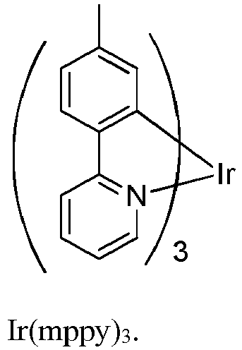
- A yellow phosphorescent dye may be selected from the following compounds:

- A blue phosphorescent dye used herein may be selected from the following compounds:

- The present invention is further illustrated in connection with the following examples.
- In this example, luminescent devices in which a hole
transport material layer 05 and an electrontransport material layer 06 in a luminescent layer have different thicknesses are manufactured, and these devices have a structure shown asFig. 1 . In the luminescent layer, the holetransport material layer 05 consists of a host material compound (2-5) TCTA, and the electrontransport material layer 06 consists of a host material compound (1-8) CzTrz and a phosphorescent dye PO-01. The difference in LUMO energy level between the host compound (2-5) TCTA and the acceptor host compound (1-8) CzTrz is more than 0.3 eV, and the difference in HOMO energy is more than 0.2 eV; and the first singlet state energy level of the exciplex is higher than the first triplet state energy level of the phosphorescent dye. The phosphorescent dye PO-01 accounts for 3 wt% of the luminescent layer. - The device of this example has the following structure.
- ITO (150 nm)/NPB (40 nm)/hole transport material layer TCTA (10 nm)/electron transport material layer compound (1-8) CzTrz + phosphorescent dye PO-01 (10-40 nm)/Bphen (20 nm)/LiF (0.5nm)/Al (150 nm)
- In this example and the description below, the unit of doping concentration of the phosphorescent dye is wt%.
- The organic electroluminescence device was manufactured as follows:
- first, a glass substrate was cleaned with a detergent and deionized water and placed under an infrared lamp for drying, and a layer of anode material was sputtered on the glass substrate with a film thickness of 150 nm;
- then, the glass substrate having the
anode 01 was placed in a vacuum chamber under a pressure of 1×10⁻⁴ Pa, and NPB was vapor deposited on the anode film as ahole transport layer 03 under such conditions, the film forming rate was 0.1 nm/s and the vapor deposited film thickness was 40 nm; a luminescent layer was vapor deposited on thehole transport layer 03 by dual-source co-evaporation, in which a hole transport material layer 05TCTA (10 nm) was vapor deposited and then an electrontransport material layer 06 CzTrz and a phosphorescent dye PO-01 were vapor deposited at the given mass percentages under a film thickness monitor while the film forming rate was controlled and the vapor deposited film thickness was controlled to be 30 nm; - on the luminescent layer, a layer of Bphen material was further vapor deposited as an
electron transport layer 07 under such conditions that the vapor deposition rate was 0.1 nm/s and the total thickness of vapor deposited film was 20 nm; and - finally, a LiF layer and an Al layer were successively vapor deposited as a cathode layer of the device by vapor deposition on the luminescent layer, in which the vapor deposition rate of the LiF layer was 0.01-0.02 nm/s and the thickness was 0.5 nm, and the vapor deposition rate of the Al layer was 1.0 nm/s and the thickness was 150 nm.
- An organic electroluminescence device was manufactured by the same method as Example 1, having the following structure:
ITO (150 nm)/NPB (40 nm)/CBP + 3 wt% PO-01(40 nm)/Bphen (20 nm)/LiF (0.5 nm)/Al (150 nm) - In another word, the luminescent layer consists of a host material CBP and a phosphorescent dye PO-01, in which the phosphorescent dye PO-01 accounts for 3 wt% of the luminescent layer. In this example and the description below, the unit of doping concentration of the phosphorescent dye is wt%.
- An organic electroluminescence device was manufactured by the same method as Example 1, having the following structure:
ITO (150 nm)/NPB (40 nm)/exciplex (TCTA and CzTrz, at the mass ratio of 1:1) + 3 wt% PO-01 (40 nm)/Alq3 (20 nm)/LiF (0.5 nm)/Al (150 nm) - In another word, the luminescent layer of this comparative example is a single layer consisting of an exciplex as host material and a phosphorescent dye PO-01 doped in the host material, in which the exciplex consists of a material TCTA having hole transport capability and a material CzTrz having electron transport capability, at the mass ratio of 1:1. The phosphorescent dye PO-01 accounts for 3 wt% of the luminescent layer.
- The properties of the organic electroluminescence devices of Example 1 and Comparative example 1 are shown in Table 1 below.
Table 1 Device Luminescent layer composition Luminous efficiency (cd/A) Luminanc e (cd/m2) External quantum efficienc y (%) Lifetime T97 (hrs) Example 1 TCTA(10)/ CzTrz: 3 wt% PO-01(10 nm) 58 1000 19 462 TCTA(10)/ CzTrz: 3 wt% PO-01(20 nm) 61 1000 21 471 TCTA(10)/ CzTrz: 3 wt% PO-01(30 nm) 64 1000 25 480 TCTA(10)/ CzTrz: 3 wt% PO-01 (40 nm) 59 1000 20 465 Comparative example 1 CBP: 3 wt% PO-01(40 nm) 55 1000 18 437 Comparative example 2 TCTA: CzTrz: 3 wt% PO-01 (40 nm) 61 1000 23 450 - It can be seen from Table 1 that the luminous efficiencies of the devices of both Example 1 and Comparative example 2, using exciplex as host, are higher than that of Comparative example 1 using the conventional host material CBP, and the lifetime of the device using exciplex as host is longer than that of Comparative example 1. The lifetime of Example 1 is longer than that of Comparative example 2, because in the exciplex system of Comparative example 2, the excited state of the donor or acceptor alone is also formed such that the donor or acceptor is easily decomposed, making the device unstable. In addition, Example 1 adopts a double doping system which is easier for control than a triple doping system adopted by Comparative example 2 in terms of process and is suitable for mass production applications.
- The device of this example has the following structure.
- ITO (150 nm)/NPB (40 nm)/TCTA (10 nm)/CzTrz+1-10 wt% phosphorescent dye PO-01(30 nm)/Bphen (20 nm)/LiF (0.5 nm)/Al (150 nm)
- The phosphorescent dye PO-01 accounts for 1-10 wt% of the luminescent layer.
- In this example, different doping concentrations of phosphorescent dye were applied in the luminescent layer for experiments, and the results were shown in Table 2.
Table 2 Luminescent layer Luminous efficiency (cd/A) Luminance (cd/m2) External quantum efficiency (%) Lifetime T97 (hrs) TCTA(10)/ CzTrz: 1 wt% PO-01(30 nm) 58 1000 14.1 435 TCTA(10)/ CzTrz: 2 wt% PO-01(30 nm) 61 1000 14.7 462 TCTA(10)/ CzTrz: 3 wt% PO-01(30 nm) 64 1000 16.1 480 TCTA(10)/ CzTrz: 5 wt% PO-01(30 nm) 57 1000 14.6 471 TCTA(10)/ CzTrz: 10 wt% PO-01(30 nm) 54 1000 12.9 443 - It can be seen from Table 2 that when the doping concentration of the phosphorescent dye in the luminescent layer is 3 wt%, both the external quantum efficiency and the lifetime of the OLED device are optimal.
- In order to evaluate the influence of the host material on the performance of the organic electroluminescence device of the present invention, an organic electroluminescence device was manufactured by the same method as Example 1, having the following structure:
ITO (150 nm)/NPB (40 nm)/hole transport material layer (material having hole transport capability) (10 nm)/electron transport material layer (material having electron transport capability + 3 wt% phosphorescent dye) (30 nm)/Bphen (20nm)/LiF (0.5nm)/Al (150 nm) - The performance of the organic electroluminescence device is shown in Table 3 below:
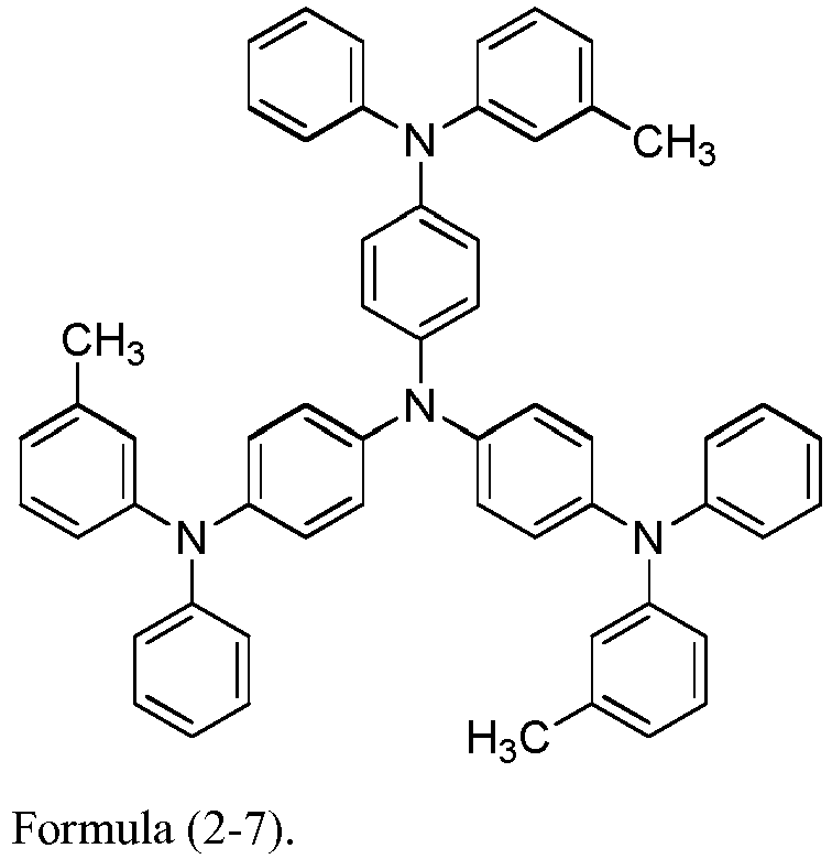
Table 3 Device Hole transport material layer Electron transport material layer Luminous efficiency (cd/A) Luminance (cd/m2) External quantum efficiency (%) Lifetime T97 (hrs) OLED1 compound (2-7) compound (1-3) + phosphorescent dye Ir(piq)3 23 1000 18 390 OLED2 compound (2-7) compound (1-7) + phosphorescent dye Ir(DBQ)2(acac) 20 1000 16 348 OLED3. compound (2-5) compound (1-1) + phosphorescent dye Ir(ppy)3 67 1000 17 390 OLED4 compound (2-1) compound (1-3) + phosphorescent dye Ir(mppy)3 63 1000 16 420 OLED5. compound (2-2) compound (1-5) + phosphorescent dye FIrPic 38 1000 14 65 - It can be seen from Table 3 that the devices of OLED1 to OLED5 in which the exciplex is formed as host on the interface between the hole
transport material layer 05 and the electrontransport material layer 06 have excellent electrical properties and increased lifetime, indicating that the triplet state energy of the TADF exciplex that is formed on the interface between the holetransport material layer 05 and the electrontransport material layer 06 is transferred to the singlet state and then transferred to the triplet state of the dopant material, so that the triplet state energy of both the host material and the dopant material are fully utilized, thereby improving the device efficiency. - The above embodiments are merely preferred embodiments for fully describing the present invention, and not intended to limit the scope of the present invention. Any equivalents or changes made by those skilled in the art on the basis of the present invention fall within the scope of the present invention. The scope of the present invention is defined by the claims.
Claims (10)
- A phosphorescent organic electroluminescence device, including a hole transport layer, a luminescent layer and an electron transport layer, which are successively laminated, wherein the luminescent layer has a double-layer structure comprising a hole transport material layer and an electron transport material layer, the hole transport material layer is arranged between the hole transport layer and the electron transport material layer, the electron transport material layer is arranged between the hole transport material layer and the electron transport layer, and an exciplex is formed on a contact interface between the hole transport material layer and the electron transport material layer;
the hole transport material layer includes a host material having hole transport capability; and
the electron transport material layer includes a host material and a phosphorescent dye doped in the host material, the host material 1 having electron transport capability;
wherein, the first triplet state energy level of the material having electron transport capability is higher than the singlet state energy level of the exciplex, with an energy gap between the material having electron transport capability and the exciplex being more than or equal to 0.2 eV; and the absolute value of HOMO energy level of the material having hole transport capability is less than or equal to 5.3 eV;
the first triplet state energy level of the material having electron transport capability is higher than the first singlet state energy level of the exciplex, with an energy gap between the material having electron transport capability and the exciplex being more than 0.2 eV; and the absolute value of LUMO energy level of the material having electron transport capability is more than 2.0 eV; the difference in LUMO energy level between the material having hole transport capability and the material having electron transport capability is more than 0.3 eV, and the difference in HOMO energy level between the material having hole transport capability and the material having electron transport capability is more than 0.2 eV; and
the first singlet state energy level of the exciplex is higher than the first triplet state energy level of the phosphorescent dye. - The phosphorescent organic electroluminescence device according to claim 1, wherein the difference in LUMO energy level between the material having hole transport capability and the material having electron transport capability is more than or equal to 0.4 eV.
- The phosphorescent organic electroluminescence device according to claim 1, , wherein the phosphorescent dye accounts for 1-10 wt% of the luminescent layer.
- The phosphorescent organic electroluminescence device according to claim 1, wherein the phosphorescent dye accounts for 3 wt% of the luminescent layer.
- The phosphorescent organic electroluminescence device according to claim 1, wherein the thickness ratio of the hole transport material layer to the electron transport material layer is 1:1 to 1:5.
- The phosphorescent organic electroluminescence device according to claim 1, wherein the thickness ratio of the hole transport material layer to the electron transport material layer is 1:3.
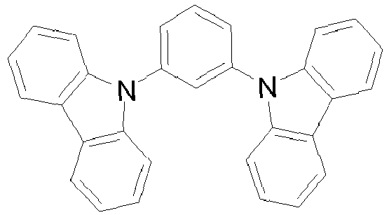
- The phosphorescent organic electroluminescence device according to claim 1, wherein the material having electron transport capability is one or more of compounds of the structural formulae (1-1) to (1-8):


- The phosphorescent organic electroluminescence device according to claim 1, wherein, the material having hole transport capability is one or more of compounds of the structural formulae (2-1) to (2-7):



- The phosphorescent organic electroluminescence device according to claim 1, wherein the phosphorescent organic electroluminescence device includes an anode, a hole transport layer, the hole transport material layer, the electron transport material layer, an electron transport layer and a cathode, which are successively laminated on a substrate.
- The phosphorescent organic electroluminescence device according to claim 9, wherein the anode and the hole transport layer has a hole injection layer arranged therebetween.
Applications Claiming Priority (2)
| Application Number | Priority Date | Filing Date | Title |
|---|---|---|---|
| CN201510952274.5A CN106898700B (en) | 2015-12-18 | 2015-12-18 | A phosphorescent organic electroluminescent device |
| PCT/CN2016/107232 WO2017101657A1 (en) | 2015-12-18 | 2016-11-25 | Organic electrophosphorescence device |
Publications (3)
| Publication Number | Publication Date |
|---|---|
| EP3370273A1 true EP3370273A1 (en) | 2018-09-05 |
| EP3370273A4 EP3370273A4 (en) | 2018-12-12 |
| EP3370273B1 EP3370273B1 (en) | 2020-05-13 |
Family
ID=59055763
Family Applications (1)
| Application Number | Title | Priority Date | Filing Date |
|---|---|---|---|
| EP16874714.5A Active EP3370273B1 (en) | 2015-12-18 | 2016-11-25 | Organic electrophosphorescence devices |
Country Status (7)
| Country | Link |
|---|---|
| US (1) | US20180375053A1 (en) |
| EP (1) | EP3370273B1 (en) |
| JP (1) | JP6701335B2 (en) |
| KR (1) | KR102114077B1 (en) |
| CN (1) | CN106898700B (en) |
| TW (1) | TWI640532B (en) |
| WO (1) | WO2017101657A1 (en) |
Families Citing this family (19)
| Publication number | Priority date | Publication date | Assignee | Title |
|---|---|---|---|---|
| CN112420965B (en) * | 2017-11-18 | 2023-10-24 | 昆山国显光电有限公司 | Organic electroluminescent devices |
| CN109994626B (en) * | 2017-12-29 | 2021-04-02 | 中节能万润股份有限公司 | Organic light-emitting composite material and organic light-emitting device comprising the same |
| CN108365112B (en) * | 2018-01-19 | 2020-06-16 | 昆山国显光电有限公司 | Electroluminescent device |
| CN109713143A (en) * | 2018-03-19 | 2019-05-03 | 广东聚华印刷显示技术有限公司 | Electroluminescent device, display device and preparation method thereof |
| CN110212102A (en) * | 2018-03-29 | 2019-09-06 | 京东方科技集团股份有限公司 | Light emitting diode with quantum dots, preparation method and display device |
| US11063224B2 (en) | 2018-05-30 | 2021-07-13 | Kunshan Go-Visionox Opto-Electronics Co., Ltd. | Organic electroluminescent device |
| CN108695440B (en) * | 2018-05-30 | 2019-07-16 | 昆山国显光电有限公司 | A kind of organic electroluminescence device |
| CN109494308A (en) * | 2018-11-21 | 2019-03-19 | 上海天马有机发光显示技术有限公司 | A kind of display panel and display device |
| KR102752374B1 (en) * | 2018-12-27 | 2025-01-08 | 엘지디스플레이 주식회사 | Organic light emitting diode and orgnic light emitting display device including the same |
| CN111490172B (en) * | 2019-05-10 | 2023-02-07 | 广东聚华印刷显示技术有限公司 | Light emitting device |
| CN112490378B (en) * | 2019-09-11 | 2022-08-16 | 江苏三月科技股份有限公司 | Organic electroluminescent device, method of manufacturing the same, and display apparatus including the same |
| CN111293228B (en) * | 2020-02-25 | 2022-10-25 | 昆山国显光电有限公司 | Light emitting device and display panel |
| CN113224244B (en) * | 2020-04-10 | 2022-12-20 | 广东聚华印刷显示技术有限公司 | Light-emitting device, preparation method thereof and display device |
| CN111943829B (en) * | 2020-07-27 | 2022-04-15 | 清华大学 | Exciplex, application thereof and organic electroluminescent device adopting exciplex |
| CN113594379A (en) * | 2020-07-27 | 2021-11-02 | 广东聚华印刷显示技术有限公司 | Electroluminescent device, manufacturing method thereof and light-emitting device |
| CN111952478B (en) * | 2020-08-25 | 2024-03-12 | 烟台大学 | Interfacial exciplex single-emitting layer white-light phosphorescent organic electroluminescent device |
| CN113471376B (en) * | 2021-06-28 | 2024-03-19 | 广东聚华印刷显示技术有限公司 | Light emitting structure, organic light emitting diode and electronic device |
| CN113444519A (en) * | 2021-07-22 | 2021-09-28 | 季华恒烨(佛山)电子材料有限公司 | Organic phosphorescent composition and preparation method and application thereof |
| TWI878660B (en) * | 2022-03-21 | 2025-04-01 | 財團法人紡織產業綜合研究所 | Electroluminescence wire |
Family Cites Families (10)
| Publication number | Priority date | Publication date | Assignee | Title |
|---|---|---|---|---|
| US7662485B2 (en) * | 2004-03-16 | 2010-02-16 | Eastman Kodak Company | White organic light-emitting devices with improved performance |
| US20070252516A1 (en) * | 2006-04-27 | 2007-11-01 | Eastman Kodak Company | Electroluminescent devices including organic EIL layer |
| US7635777B2 (en) * | 2006-12-11 | 2009-12-22 | General Electric Company | Carbazolyl monomers and polymers |
| US8034465B2 (en) * | 2007-06-20 | 2011-10-11 | Global Oled Technology Llc | Phosphorescent oled having double exciton-blocking layers |
| US20090191427A1 (en) * | 2008-01-30 | 2009-07-30 | Liang-Sheng Liao | Phosphorescent oled having double hole-blocking layers |
| KR101635726B1 (en) * | 2008-08-08 | 2016-07-05 | 유니버시티 오브 노스 텍사스 | Organic light-emitting diodes from homoleptic square planar complexes |
| KR101419810B1 (en) * | 2012-04-10 | 2014-07-15 | 서울대학교산학협력단 | Organic light-emitting diode comprising exciplex forming co-host |
| CN104073246A (en) * | 2013-03-29 | 2014-10-01 | 海洋王照明科技股份有限公司 | Organic electrophosphorescent main body material as well as preparation method thereof and organic electroluminescence device |
| JP6468579B2 (en) * | 2013-05-10 | 2019-02-13 | 国立大学法人山形大学 | Blue organic electroluminescence device |
| KR20150122005A (en) * | 2014-04-22 | 2015-10-30 | 제일모직주식회사 | Compound for organic optoelectric device and composition and organic optoelectric device and display device |
-
2015
- 2015-12-18 CN CN201510952274.5A patent/CN106898700B/en active Active
-
2016
- 2016-11-25 KR KR1020187014719A patent/KR102114077B1/en active Active
- 2016-11-25 US US15/781,439 patent/US20180375053A1/en not_active Abandoned
- 2016-11-25 EP EP16874714.5A patent/EP3370273B1/en active Active
- 2016-11-25 JP JP2018526171A patent/JP6701335B2/en active Active
- 2016-11-25 WO PCT/CN2016/107232 patent/WO2017101657A1/en not_active Ceased
- 2016-11-30 TW TW105139550A patent/TWI640532B/en active
Also Published As
| Publication number | Publication date |
|---|---|
| JP2019504471A (en) | 2019-02-14 |
| EP3370273A4 (en) | 2018-12-12 |
| TWI640532B (en) | 2018-11-11 |
| JP6701335B2 (en) | 2020-05-27 |
| WO2017101657A1 (en) | 2017-06-22 |
| CN106898700B (en) | 2019-06-25 |
| TW201722977A (en) | 2017-07-01 |
| EP3370273B1 (en) | 2020-05-13 |
| KR102114077B1 (en) | 2020-05-22 |
| CN106898700A (en) | 2017-06-27 |
| KR20180074761A (en) | 2018-07-03 |
| US20180375053A1 (en) | 2018-12-27 |
Similar Documents
| Publication | Publication Date | Title |
|---|---|---|
| EP3370273B1 (en) | Organic electrophosphorescence devices | |
| CN104576950B (en) | Organic luminescent device | |
| CN109378392B (en) | An organic electroluminescent device and display device | |
| KR20080106130A (en) | Organic Optoelectronic Devices and Materials Used Therein | |
| KR20130115027A (en) | Organic light-emitting diode comprising exciplex forming co-host | |
| JP2004288619A (en) | High efficiency organic electroluminescent device | |
| WO2012132842A1 (en) | Organic electroluminescent element | |
| CN108832008B (en) | Application of exciplex in organic light-emitting diode | |
| CN102779948B (en) | White color organic electroluminescence device and manufacture method thereof | |
| WO2013174104A1 (en) | Organic electroluminescent device and manufacturing method thereof | |
| CN107452886A (en) | A kind of laminated film and Organic Light Emitting Diode and preparation method thereof | |
| WO2021077486A1 (en) | Oled display panel and display device | |
| CN110492007A (en) | A kind of acridine compounds and its application in organic electroluminescence devices | |
| CN104518121B (en) | A kind of organic electroluminescence device | |
| CN100471352C (en) | An organic electroluminescent device | |
| KR20160047297A (en) | Organic electro luminescence device | |
| TWI447982B (en) | Organic light emitting device | |
| TW201526326A (en) | Organic light emitting device | |
| CN111416047B (en) | Fluorescence/phosphorescence hybrid white light organic light-emitting diode and preparation method thereof | |
| CN105870350B (en) | Organic luminescent device | |
| KR102791024B1 (en) | Organic light emitting device | |
| KR20100133352A (en) | Organic photoelectric device | |
| CN113328045A (en) | Light emitting device and light emitting apparatus | |
| TW200423813A (en) | Organic light-emitting diode containing fullerene as a hole-injection modification layer or hole-transporting layer | |
| CN115835673B (en) | White light organic electroluminescent device and application thereof |
Legal Events
| Date | Code | Title | Description |
|---|---|---|---|
| STAA | Information on the status of an ep patent application or granted ep patent |
Free format text: STATUS: THE INTERNATIONAL PUBLICATION HAS BEEN MADE |
|
| PUAI | Public reference made under article 153(3) epc to a published international application that has entered the european phase |
Free format text: ORIGINAL CODE: 0009012 |
|
| STAA | Information on the status of an ep patent application or granted ep patent |
Free format text: STATUS: REQUEST FOR EXAMINATION WAS MADE |
|
| 17P | Request for examination filed |
Effective date: 20180528 |
|
| AK | Designated contracting states |
Kind code of ref document: A1 Designated state(s): AL AT BE BG CH CY CZ DE DK EE ES FI FR GB GR HR HU IE IS IT LI LT LU LV MC MK MT NL NO PL PT RO RS SE SI SK SM TR |
|
| AX | Request for extension of the european patent |
Extension state: BA ME |
|
| A4 | Supplementary search report drawn up and despatched |
Effective date: 20181109 |
|
| RIC1 | Information provided on ipc code assigned before grant |
Ipc: H01L 51/50 20060101AFI20181105BHEP |
|
| DAV | Request for validation of the european patent (deleted) | ||
| DAX | Request for extension of the european patent (deleted) | ||
| STAA | Information on the status of an ep patent application or granted ep patent |
Free format text: STATUS: EXAMINATION IS IN PROGRESS |
|
| 17Q | First examination report despatched |
Effective date: 20190412 |
|
| REG | Reference to a national code |
Ref country code: DE Ref legal event code: R079 Ref document number: 602016036581 Country of ref document: DE Free format text: PREVIOUS MAIN CLASS: H01L0051500000 Ipc: H01L0051540000 |
|
| GRAP | Despatch of communication of intention to grant a patent |
Free format text: ORIGINAL CODE: EPIDOSNIGR1 |
|
| STAA | Information on the status of an ep patent application or granted ep patent |
Free format text: STATUS: GRANT OF PATENT IS INTENDED |
|
| RIC1 | Information provided on ipc code assigned before grant |
Ipc: H01L 51/54 20060101AFI20200123BHEP |
|
| INTG | Intention to grant announced |
Effective date: 20200207 |
|
| GRAS | Grant fee paid |
Free format text: ORIGINAL CODE: EPIDOSNIGR3 |
|
| GRAA | (expected) grant |
Free format text: ORIGINAL CODE: 0009210 |
|
| STAA | Information on the status of an ep patent application or granted ep patent |
Free format text: STATUS: THE PATENT HAS BEEN GRANTED |
|
| AK | Designated contracting states |
Kind code of ref document: B1 Designated state(s): AL AT BE BG CH CY CZ DE DK EE ES FI FR GB GR HR HU IE IS IT LI LT LU LV MC MK MT NL NO PL PT RO RS SE SI SK SM TR |
|
| REG | Reference to a national code |
Ref country code: GB Ref legal event code: FG4D |
|
| REG | Reference to a national code |
Ref country code: CH Ref legal event code: EP |
|
| REG | Reference to a national code |
Ref country code: DE Ref legal event code: R096 Ref document number: 602016036581 Country of ref document: DE |
|
| REG | Reference to a national code |
Ref country code: AT Ref legal event code: REF Ref document number: 1271389 Country of ref document: AT Kind code of ref document: T Effective date: 20200615 |
|
| REG | Reference to a national code |
Ref country code: LT Ref legal event code: MG4D |
|
| REG | Reference to a national code |
Ref country code: NL Ref legal event code: MP Effective date: 20200513 |
|
| PG25 | Lapsed in a contracting state [announced via postgrant information from national office to epo] |
Ref country code: SE Free format text: LAPSE BECAUSE OF FAILURE TO SUBMIT A TRANSLATION OF THE DESCRIPTION OR TO PAY THE FEE WITHIN THE PRESCRIBED TIME-LIMIT Effective date: 20200513 Ref country code: LT Free format text: LAPSE BECAUSE OF FAILURE TO SUBMIT A TRANSLATION OF THE DESCRIPTION OR TO PAY THE FEE WITHIN THE PRESCRIBED TIME-LIMIT Effective date: 20200513 Ref country code: GR Free format text: LAPSE BECAUSE OF FAILURE TO SUBMIT A TRANSLATION OF THE DESCRIPTION OR TO PAY THE FEE WITHIN THE PRESCRIBED TIME-LIMIT Effective date: 20200814 Ref country code: NO Free format text: LAPSE BECAUSE OF FAILURE TO SUBMIT A TRANSLATION OF THE DESCRIPTION OR TO PAY THE FEE WITHIN THE PRESCRIBED TIME-LIMIT Effective date: 20200813 Ref country code: IS Free format text: LAPSE BECAUSE OF FAILURE TO SUBMIT A TRANSLATION OF THE DESCRIPTION OR TO PAY THE FEE WITHIN THE PRESCRIBED TIME-LIMIT Effective date: 20200913 Ref country code: PT Free format text: LAPSE BECAUSE OF FAILURE TO SUBMIT A TRANSLATION OF THE DESCRIPTION OR TO PAY THE FEE WITHIN THE PRESCRIBED TIME-LIMIT Effective date: 20200914 Ref country code: FI Free format text: LAPSE BECAUSE OF FAILURE TO SUBMIT A TRANSLATION OF THE DESCRIPTION OR TO PAY THE FEE WITHIN THE PRESCRIBED TIME-LIMIT Effective date: 20200513 |
|
| PG25 | Lapsed in a contracting state [announced via postgrant information from national office to epo] |
Ref country code: RS Free format text: LAPSE BECAUSE OF FAILURE TO SUBMIT A TRANSLATION OF THE DESCRIPTION OR TO PAY THE FEE WITHIN THE PRESCRIBED TIME-LIMIT Effective date: 20200513 Ref country code: HR Free format text: LAPSE BECAUSE OF FAILURE TO SUBMIT A TRANSLATION OF THE DESCRIPTION OR TO PAY THE FEE WITHIN THE PRESCRIBED TIME-LIMIT Effective date: 20200513 Ref country code: LV Free format text: LAPSE BECAUSE OF FAILURE TO SUBMIT A TRANSLATION OF THE DESCRIPTION OR TO PAY THE FEE WITHIN THE PRESCRIBED TIME-LIMIT Effective date: 20200513 Ref country code: BG Free format text: LAPSE BECAUSE OF FAILURE TO SUBMIT A TRANSLATION OF THE DESCRIPTION OR TO PAY THE FEE WITHIN THE PRESCRIBED TIME-LIMIT Effective date: 20200813 |
|
| REG | Reference to a national code |
Ref country code: AT Ref legal event code: MK05 Ref document number: 1271389 Country of ref document: AT Kind code of ref document: T Effective date: 20200513 |
|
| PG25 | Lapsed in a contracting state [announced via postgrant information from national office to epo] |
Ref country code: NL Free format text: LAPSE BECAUSE OF FAILURE TO SUBMIT A TRANSLATION OF THE DESCRIPTION OR TO PAY THE FEE WITHIN THE PRESCRIBED TIME-LIMIT Effective date: 20200513 Ref country code: AL Free format text: LAPSE BECAUSE OF FAILURE TO SUBMIT A TRANSLATION OF THE DESCRIPTION OR TO PAY THE FEE WITHIN THE PRESCRIBED TIME-LIMIT Effective date: 20200513 |
|
| PG25 | Lapsed in a contracting state [announced via postgrant information from national office to epo] |
Ref country code: IT Free format text: LAPSE BECAUSE OF FAILURE TO SUBMIT A TRANSLATION OF THE DESCRIPTION OR TO PAY THE FEE WITHIN THE PRESCRIBED TIME-LIMIT Effective date: 20200513 Ref country code: AT Free format text: LAPSE BECAUSE OF FAILURE TO SUBMIT A TRANSLATION OF THE DESCRIPTION OR TO PAY THE FEE WITHIN THE PRESCRIBED TIME-LIMIT Effective date: 20200513 Ref country code: DK Free format text: LAPSE BECAUSE OF FAILURE TO SUBMIT A TRANSLATION OF THE DESCRIPTION OR TO PAY THE FEE WITHIN THE PRESCRIBED TIME-LIMIT Effective date: 20200513 Ref country code: EE Free format text: LAPSE BECAUSE OF FAILURE TO SUBMIT A TRANSLATION OF THE DESCRIPTION OR TO PAY THE FEE WITHIN THE PRESCRIBED TIME-LIMIT Effective date: 20200513 Ref country code: SM Free format text: LAPSE BECAUSE OF FAILURE TO SUBMIT A TRANSLATION OF THE DESCRIPTION OR TO PAY THE FEE WITHIN THE PRESCRIBED TIME-LIMIT Effective date: 20200513 Ref country code: ES Free format text: LAPSE BECAUSE OF FAILURE TO SUBMIT A TRANSLATION OF THE DESCRIPTION OR TO PAY THE FEE WITHIN THE PRESCRIBED TIME-LIMIT Effective date: 20200513 Ref country code: CZ Free format text: LAPSE BECAUSE OF FAILURE TO SUBMIT A TRANSLATION OF THE DESCRIPTION OR TO PAY THE FEE WITHIN THE PRESCRIBED TIME-LIMIT Effective date: 20200513 Ref country code: RO Free format text: LAPSE BECAUSE OF FAILURE TO SUBMIT A TRANSLATION OF THE DESCRIPTION OR TO PAY THE FEE WITHIN THE PRESCRIBED TIME-LIMIT Effective date: 20200513 |
|
| REG | Reference to a national code |
Ref country code: DE Ref legal event code: R097 Ref document number: 602016036581 Country of ref document: DE |
|
| PG25 | Lapsed in a contracting state [announced via postgrant information from national office to epo] |
Ref country code: SK Free format text: LAPSE BECAUSE OF FAILURE TO SUBMIT A TRANSLATION OF THE DESCRIPTION OR TO PAY THE FEE WITHIN THE PRESCRIBED TIME-LIMIT Effective date: 20200513 Ref country code: PL Free format text: LAPSE BECAUSE OF FAILURE TO SUBMIT A TRANSLATION OF THE DESCRIPTION OR TO PAY THE FEE WITHIN THE PRESCRIBED TIME-LIMIT Effective date: 20200513 |
|
| PLBE | No opposition filed within time limit |
Free format text: ORIGINAL CODE: 0009261 |
|
| STAA | Information on the status of an ep patent application or granted ep patent |
Free format text: STATUS: NO OPPOSITION FILED WITHIN TIME LIMIT |
|
| 26N | No opposition filed |
Effective date: 20210216 |
|
| PG25 | Lapsed in a contracting state [announced via postgrant information from national office to epo] |
Ref country code: SI Free format text: LAPSE BECAUSE OF FAILURE TO SUBMIT A TRANSLATION OF THE DESCRIPTION OR TO PAY THE FEE WITHIN THE PRESCRIBED TIME-LIMIT Effective date: 20200513 |
|
| PG25 | Lapsed in a contracting state [announced via postgrant information from national office to epo] |
Ref country code: MC Free format text: LAPSE BECAUSE OF FAILURE TO SUBMIT A TRANSLATION OF THE DESCRIPTION OR TO PAY THE FEE WITHIN THE PRESCRIBED TIME-LIMIT Effective date: 20200513 |
|
| REG | Reference to a national code |
Ref country code: CH Ref legal event code: PL |
|
| PG25 | Lapsed in a contracting state [announced via postgrant information from national office to epo] |
Ref country code: LU Free format text: LAPSE BECAUSE OF NON-PAYMENT OF DUE FEES Effective date: 20201125 |
|
| REG | Reference to a national code |
Ref country code: BE Ref legal event code: MM Effective date: 20201130 |
|
| PG25 | Lapsed in a contracting state [announced via postgrant information from national office to epo] |
Ref country code: LI Free format text: LAPSE BECAUSE OF NON-PAYMENT OF DUE FEES Effective date: 20201130 Ref country code: CH Free format text: LAPSE BECAUSE OF NON-PAYMENT OF DUE FEES Effective date: 20201130 |
|
| PG25 | Lapsed in a contracting state [announced via postgrant information from national office to epo] |
Ref country code: IE Free format text: LAPSE BECAUSE OF NON-PAYMENT OF DUE FEES Effective date: 20201125 |
|
| PG25 | Lapsed in a contracting state [announced via postgrant information from national office to epo] |
Ref country code: TR Free format text: LAPSE BECAUSE OF FAILURE TO SUBMIT A TRANSLATION OF THE DESCRIPTION OR TO PAY THE FEE WITHIN THE PRESCRIBED TIME-LIMIT Effective date: 20200513 Ref country code: MT Free format text: LAPSE BECAUSE OF FAILURE TO SUBMIT A TRANSLATION OF THE DESCRIPTION OR TO PAY THE FEE WITHIN THE PRESCRIBED TIME-LIMIT Effective date: 20200513 Ref country code: CY Free format text: LAPSE BECAUSE OF FAILURE TO SUBMIT A TRANSLATION OF THE DESCRIPTION OR TO PAY THE FEE WITHIN THE PRESCRIBED TIME-LIMIT Effective date: 20200513 |
|
| PG25 | Lapsed in a contracting state [announced via postgrant information from national office to epo] |
Ref country code: MK Free format text: LAPSE BECAUSE OF FAILURE TO SUBMIT A TRANSLATION OF THE DESCRIPTION OR TO PAY THE FEE WITHIN THE PRESCRIBED TIME-LIMIT Effective date: 20200513 |
|
| PG25 | Lapsed in a contracting state [announced via postgrant information from national office to epo] |
Ref country code: BE Free format text: LAPSE BECAUSE OF NON-PAYMENT OF DUE FEES Effective date: 20201130 |
|
| REG | Reference to a national code |
Ref country code: DE Ref legal event code: R079 Ref document number: 602016036581 Country of ref document: DE Free format text: PREVIOUS MAIN CLASS: H01L0051540000 Ipc: H10K0085000000 |
|
| P01 | Opt-out of the competence of the unified patent court (upc) registered |
Effective date: 20230526 |
|
| PGFP | Annual fee paid to national office [announced via postgrant information from national office to epo] |
Ref country code: DE Payment date: 20251117 Year of fee payment: 10 |
|
| PGFP | Annual fee paid to national office [announced via postgrant information from national office to epo] |
Ref country code: GB Payment date: 20251126 Year of fee payment: 10 |
|
| PGFP | Annual fee paid to national office [announced via postgrant information from national office to epo] |
Ref country code: FR Payment date: 20251127 Year of fee payment: 10 |