EP3367580A1 - Transmission arrangement for full-duplex communication - Google Patents
Transmission arrangement for full-duplex communication Download PDFInfo
- Publication number
- EP3367580A1 EP3367580A1 EP17158402.2A EP17158402A EP3367580A1 EP 3367580 A1 EP3367580 A1 EP 3367580A1 EP 17158402 A EP17158402 A EP 17158402A EP 3367580 A1 EP3367580 A1 EP 3367580A1
- Authority
- EP
- European Patent Office
- Prior art keywords
- pair
- terminals
- adder
- coupled
- input terminals
- Prior art date
- Legal status (The legal status is an assumption and is not a legal conclusion. Google has not performed a legal analysis and makes no representation as to the accuracy of the status listed.)
- Granted
Links
Images


Classifications
-
- H—ELECTRICITY
- H04—ELECTRIC COMMUNICATION TECHNIQUE
- H04B—TRANSMISSION
- H04B3/00—Line transmission systems
- H04B3/02—Details
- H04B3/20—Reducing echo effects or singing; Opening or closing transmitting path; Conditioning for transmission in one direction or the other
- H04B3/23—Reducing echo effects or singing; Opening or closing transmitting path; Conditioning for transmission in one direction or the other using a replica of transmitted signal in the time domain, e.g. echo cancellers
- H04B3/237—Reducing echo effects or singing; Opening or closing transmitting path; Conditioning for transmission in one direction or the other using a replica of transmitted signal in the time domain, e.g. echo cancellers using two adaptive filters, e.g. for near end and for end echo cancelling
-
- H—ELECTRICITY
- H04—ELECTRIC COMMUNICATION TECHNIQUE
- H04B—TRANSMISSION
- H04B3/00—Line transmission systems
- H04B3/02—Details
- H04B3/20—Reducing echo effects or singing; Opening or closing transmitting path; Conditioning for transmission in one direction or the other
- H04B3/23—Reducing echo effects or singing; Opening or closing transmitting path; Conditioning for transmission in one direction or the other using a replica of transmitted signal in the time domain, e.g. echo cancellers
-
- H—ELECTRICITY
- H04—ELECTRIC COMMUNICATION TECHNIQUE
- H04M—TELEPHONIC COMMUNICATION
- H04M11/00—Telephonic communication systems specially adapted for combination with other electrical systems
- H04M11/06—Simultaneous speech and data transmission, e.g. telegraphic transmission over the same conductors
- H04M11/062—Simultaneous speech and data transmission, e.g. telegraphic transmission over the same conductors using different frequency bands for speech and other data
Definitions
- the present invention relates to echo suppression for full-duplex communication systems.
- DMT Discrete Multi-Tone
- full-duplex is particularly challenging as new impairments arise, such as the undesired transmit echo signal that leaks into the useful receive signal.
- Time Division Duplexing such as in use in G.fast
- FDD Frequency Division Duplexing
- the transmitter and the receiver are active at the same time, and one has to come up with a solution to efficiently suppress the undesired echo signal from the receive signal.
- the transmitter differential output and the receiver differential input are connected to the transmission line through a so-called hybrid network.
- the hybrid network is designed to subtract the current transmit voltage from the current line voltage at the receiver input, typically by means of hybrid coils or some resistive network.
- the hybrid is only designed to suppress the immediate transmit voltage, and the various delayed reflections of the transmit signal arising from impedance mismatches along the loop or cable plant (bridged tap, passive couplers, etc) and echoing back into the receiver through the receive path cannot be distinguished from the useful receive signal and therefore cannot be suppressed by the hybrid network.
- the hybrid network is to be complemented with further echo suppression techniques in order to reduce that extra background noise and to achieve higher data throughputs.
- the residual echo channel through the hybrid is estimated by means of some probing signals, and the residual echo signal is re-generated in the digital domain from the transmit samples, converted in the analog domain by means of an additional Digital to Analog Converter (DAC), and subtracted from the receive signal in the analog domain so as to get an almost echo-free signal at the input of the ADC.
- DAC Digital to Analog Converter
- a new transmission arrangement for coupling a pair of transmit output terminals to a pair of medium terminals coupled a transmission medium, and the pair of medium terminals to a pair of receive input terminals, the pairs of transmit output terminals, receive input terminals and medium terminals carrying opposite-polarity signals.
- the transmission arrangement comprises a first adder and a second adder with respective first and second adder input terminals and respective adder output terminals.
- the pair of transmit output terminals is coupled to the pair of first adder input terminals, and is further coupled through respective first impedances to the pair of second adder input terminals and to the pair of medium terminals, with the first and second adder input terminals being respectively coupled to opposite-polarity transmit output terminals.
- the pair of receive input terminals is coupled to the pair of adder output terminals.
- the first impedances individually comprise a first resistor coupled in parallel with a first capacitor.
- the first and second adders individually comprise second and third capacitors between the respective first and second adder input terminals and a common terminal, and a feedback network between the adder output terminal and the common terminal.
- the first capacitors have a reactance value that matches the difference between the reactance values of the second and third capacitors.
- the first resistors are matching resistors whose resistance value is determined for an input impedance of the transmission arrangement to match a characteristic impedance of the transmission medium.
- the transmission arrangement further comprises an adjustment circuit for dynamically adjusting the resistance value of the first resistors.
- the first and second adders individually comprise, as feedback network, a fourth capacitor coupled between the adder output terminal and the common terminal.
- the first and second adders further individually comprise a third adder input terminal, and a fifth capacitor between the third adder input terminal and the common terminal.
- a further pair of transmit output terminals configured to output a differential echo cancellation signal is coupled to the pair of third adder input terminals.
- the first and second adders further individually comprise a high-gain differential amplifier with a pair of amplifier input terminals, the inverting terminal of which being coupled to the common terminal, and an amplifier output terminal coupled to the adder output terminal.
- the first and second adders form part of a receiver differential amplifier with a pair of amplifier input terminals coupled to the pair of common terminals, and a pair of amplifier output terminals coupled to the pair of adder output terminals.
- Such a transmission arrangement is typically embedded within an Integrated Circuit (IC), and further forms part of an access node (or access concentrator), such as a Cable Modem Termination System (CMTS), a Distribution Point Unit (DPU), a Digital Subscriber Line Access Multiplexer (DSLAM), or a wireless base station (eNodeB, wifi access point, etc), or forms part of a subscriber device, such as a modem, a switch, a router, or a user terminal (laptop, smart phone, etc).
- CMTS Cable Modem Termination System
- DPU Distribution Point Unit
- DSLAM Digital Subscriber Line Access Multiplexer
- eNodeB wireless base station
- eNodeB wireless base station
- transformer-based or resistor-based circuits have been proposed for the design of hybrid networks.
- Transformer-based hybrids make use of transformers wired in such a way to achieve high isolation between certain ports and low insertion loss between other ports.
- line transformers are often used. These circuits currently only exist as discrete components and are rather bulky (> 1 mm 3 ). Trying to integrate these components on an IC would drastically reduce performance (loss, bandwidth, etc).
- Resistor-based hybrids which have been demonstrated as discrete or on-chip solutions, can provide similar isolation and loss as transformer-based hybrids.
- resistors generate thermal noise, and their various contributions to the total receive noise power may not be negligible when the hybrid is operated over a wide frequency range (e.g., 1.2 GHz). This directly translates into a lower Signal to Noise Ratio (SNR) at the receiver, and hence a lower achievable data rate.
- SNR Signal to Noise Ratio
- a new hybrid design is proposed (capacitive hybrid hereinafter).
- the new design includes two adders.
- Each adder is equipped with two signal input terminals for picking up respective shares of two opposite-polarity transmit voltages across a matching resistor, and another (as-high-as-possible) share of a receive voltage.
- Capacitors with low capacitance values are provisioned in series along the two input branches of the adder to sink little current from the main current driving the transmission line and to guarantee low insertion loss for the transmit signal.
- Another capacitor is added in parallel with the matching resistor in order to compensate for the phase shift difference through the two input capacitors and thus to achieve perfect echo cancellation at the common sinking terminal of the adder.
- Yet another capacitor is added in the feedback loop of the adder to control the receive gain and make it frequency-independent. Inherently, these capacitors do not generate thermal noise and thus greatly improve the receiver SNR.
- the matching resistor which is the only remaining resistive component in the capacitive hybrid generating noise, has a resistance value for the input impedance of the hybrid as seen through the line terminals to match a nominal characteristic impedance of the transmission medium, typically 75 ⁇ for a coaxial cable and 100 ⁇ for a twisted copper pair, taking duly account of the winding ratio of the line transformer.
- the value of the matching resistor can be dynamically adjusted by means of an adjustment circuit to fit the real part of the actual characteristic impedance of the transmission medium and to minimize the return loss.
- a communication unit 1 for communication over a wired transmission medium with one or more peer communication units The communication unit 1 typically forms part of an access node or a CPE.
- the communication unit 1 uses Discrete Multi-Tone (DMT) modulation over closely-spaced orthogonal carriers (a.k.a. tones or bins), and operates in full-duplex mode, that is to say the same carriers are simultaneously used for both downstream (towards the subscriber premises) and upstream (from the subscriber premises) communications.
- DMT Discrete Multi-Tone
- the aggregate capacity is doubled when compared to legacy techniques, such as FDD used for DOCSIS or xDSL communications, or TDD used for G.fast communications.
- the communication unit 1 comprises a transmitter 10 with two differential transmit output terminals 101 and 102 carrying opposite-polarity transmit voltages +V TX and -V TX , and a receiver 20 with two differential receive input terminals 105 and 106 carrying opposite-polarity receive voltages +V RX and -V RX .
- the communication unit 1 further comprises a hybrid 100 coupled to the two transmit output terminals 101 and 102 and to the two receive input terminals 105 and 106, and further coupled to two line terminals 103 and 104 carrying opposite-polarity line voltages +V LINE and -V LINE .
- the line terminals 105 and 106 are further coupled to a transmission medium through a line transformer 30 for DC-isolating the communication unit 1 from the transmission medium.
- the transmission medium is depicted as an Unshielded Twisted Pair (UTP) 40, although the present invention is similarly applicable to other transmission media, such as TV broadcast coaxial cables.
- UTP Unshielded Twisted Pair
- the transmission line 40 is terminated with a load impedance Z L .
- the line voltages +V LINE and -V LINE encompass both respective transmit line voltages +V LINE_TX and -V LINE_TX on account of the transmit voltages +V TX and -V TX being applied over the transmit output terminals 101 and 102, and respective receive line voltages +V LINE_RX and -V LINE_RX on account of a transmit voltage being remotely applied over the transmission line 40 in the reverse direction by a peer communication unit.
- the hybrid 100 is configured to pass the differential transmit voltage present on the two transmit output terminals 101 and 102 towards the line terminals 103 and 104 and the differential receive voltage present on the line terminals 103 and 104 towards the receive input terminals 105 and 106 with low insertion loss, while achieving high isolation between the transmit output terminals 101 and 102 and the receive input terminals 105 and 106.
- V RMS_TX and V RMS_LINE_RX respectively denote the Root Mean Square (RMS) value of the transmit output voltage V TX at the output terminals 101 and 102 of the transmitter 10 and the RMS value of the receive line voltage V LINE_RX at the line terminals 103 and 104.
- RMS Root Mean Square
- the transmitter 10 and the receiver 20 comprise an analog part and a digital part.
- the transmit analog part comprises a Digital-to-Analog Converter 12 (or DAC), and a line driver 13 for amplifying the transmit signal and for driving the transmission line 40.
- the line driver 13 has Z 0 as output impedance, which output impedance being evenly balanced between the two output terminals 101 and 102.
- the receive analog part comprises a Low-Noise Amplifier 23 (or LNA) for amplifying the receive signal with as little noise as possible, and an Analog-to-Digital Converter 22 (or ADC).
- LNA Low-Noise Amplifier
- ADC Analog-to-Digital Converter
- the communication unit 1 may further include protection circuitry for protecting against any current or voltage surge occurring over the transmission line 40. Still for instance, the communication unit 1 may further comprise additional amplification stages along the receive path.
- the digital part is configured to operate downstream and upstream communication channels for conveying user and control traffic over the transmission line 40.
- the digital part comprises a transmit digital part 11 for encoding and modulating user and control data into DMT symbols, and a receive digital part 21 for demodulating and decoding user and control data from DMT symbols.
- the transmit digital part 11 supplies the cyclically-extended digital time samples to the DAC 12 for further analog conversion.
- the ADC 22 supplies the digital time samples of the amplified receive signal to the receive digital part 21 for the following receive steps to be performed:
- Some of these transmit or receive steps can be omitted, or some additional steps can be present, depending on the exact digital communication technology being used.
- the transmit digital part 11 and the receive digital part 21 are typically implemented by means of one or more processors.
- a processor should not be construed to refer exclusively to hardware capable of executing software, and may implicitly include, without limitation, Digital Signal Processor (DSP), Application Specific Integrated Circuit (ASIC), Field Programmable Gate Array (FPGA), etc.
- DSP Digital Signal Processor
- ASIC Application Specific Integrated Circuit
- FPGA Field Programmable Gate Array
- RAM Random Access Memory
- non volatile storage may also be included.
- the hybrid 100 is a fully-balanced transmission arrangement comprising a first adder 110 and a second adder 120.
- the first adder comprises input terminals 111 and 112, an output terminal 114, and an op-amp 116.
- the second adder 120 similarly comprises input terminals 121 and 122, an output terminal 124, and an op-amp 126.
- the first transmit output terminal 101 is coupled to a first terminal of a first impedance and to the first input terminal 111 of the first adder 110.
- the second terminal of the first impedance is coupled to the line terminal 103 and to the second input terminal 122 of the second adder 120.
- the second transmit output terminal 102 is coupled to a first terminal of a second impedance and to the first input terminal 121 of the second adder 120.
- the second terminal of the second impedance is coupled to the line terminal 104 and to the second input terminal 112 of the first adder 110.
- the first and second impedances have a common value Z 1 , and comprise a resistor R1 in parallel with a capacitor C1.
- the output terminals 114 and 124 of the first adder 110 and the second adder 120 are coupled to the respective receive input terminals 105 and 106.
- the input terminals 111 and 112 of the first adder 110 are coupled to the inverting terminal of the op-amp 116 through respective capacitors C2 and C3, the inverting terminal of the op-amp 116 acting as a common terminal 115 of the first adder 110.
- the output terminal 114 of the first adder 110 is looped back to the common terminal 115 through a capacitor C4.
- the non-inverting terminal of the op-amp 116 is grounded.
- the input terminals 121 and 122 of the second adder 120 are coupled to the inverting terminal of the op-amp 126 through respective capacitors C2 and C3, the inverting terminal of the op-amp 126 acting as a common terminal 125 of the second adder 120.
- the output terminal 124 of the first adder 120 is coupled to the common terminal 125 through a capacitor C4.
- the non-inverting terminal of the op-amp 126 is grounded.
- the hybrid is designed to subtract the current transmit voltage from the current line voltage, and is thus unable to cope with the delayed signal reflections arising from impedance mismatches along the loop or cable plant (bridged tap, passive couplers, etc) and echoing back into the receiver along the receive path.
- these various echo residues need to be estimated, re-generated in the digital domain, converted in the analog domain by means of an additional DAC , and subtracted from the line signal in the analog domain.
- the first adder 110 and second adder 120 then accommodate respective third input terminals 113 and 123 coupled to respective differential output terminals 107 and 108 carrying opposite-polarity echo cancellation voltages +V E and -V E generated by an additional DAC 14 (or EDAC).
- the third input terminals 113 and 123 are coupled to the respective common terminals 115 and 125 through a capacitor C5.
- the transmission arrangement as per fig. 2 can be analyzed by means of the superposition principle so as to de-correlate transmission from reception.
- the transmit output terminals 101 and 102 are fed with a differential transmit voltage ⁇ V TX only and that no transmit voltage is applied at the far-end of the transmission line 40, meaning no receive voltages ⁇ V LINE_RX is present on the line terminals 103 and 104, such as depicted in fig. 3A (TX only).
- E TX ⁇ ⁇ E TX +
- R L load resistor
- V TX 1 ⁇ denote the voltages appearing at the transmit output terminals 101 and 102 when no voltage is being received from the line.
- V TX 1 + Z TX Z TX + R 0 E TX ⁇
- V LINE_TX ⁇ Z 4 Z 4 + Z 1
- V TX 1 ⁇ Z 4 Z 4 + Z 1 Z TX Z TX + R 0 E TX ⁇
- Z 4 ⁇ R L 2 ⁇ C 3 R L 2 1 + j ⁇ C 3
- R L 2 R L 2 + j ⁇ C 3 R L
- i 1 and i 3 denote the currents entering the first input terminals of the adders 110 and 120 respectively
- i 4 and i 2 denote the current entering the second input terminals of the adders 110 and 120 respectively.
- i L denote the current through the load R L .
- V TX 1 + I 1 j ⁇ C 2
- V TX 1 + ⁇ V LINE_TX + Z 1 I 2 + V LINE_TX 1 + ⁇ V LINE_TX ⁇ R L , or, with further regard to eq.
- the transmission line 40 is loaded with a total impedance Z RX given by: Z RX 2 ⁇ Z 3 ⁇ Z 1 + Z 2 ⁇ R O 2
- V LINE_RX ⁇ resp. V TX 2 ⁇ , denote the voltages produced by the transformer emf at the line terminals 103 and 104, resp. the voltages appearing at the transmit output terminals 101 and 102, when a voltage is being remotely applied over the line and no transmit voltage is being inserted by the transmitter.
- the reactance value of the capacitor C 1 shall substantially match the difference between the reactance value of the first input branch of one adder and the reactance value of the second input branch of the other adder, namely 1/C 2 - 1/C 3 , so as there are antiphase input currents at the common terminal of the adders.
- the capacitance value of the capacitor C 3 shall be chosen sufficiently small in order to have the lowest insertion loss for the transmit signal.
- the chosen capacitance value shall substantially match eq. (21), which is possible as eq. (20) and (21) leave some degree of freedom for selecting a capacitance value for the capacitor C 2 .
- the capacitance value of the capacitor C 4 determines the receive gain across the opamps 116 and 126 as per eq. (27).
- the capacitance value of the capacitor C 5 determines the insertion gain of the echo cancellation voltage V E ⁇ .
- the resistor R 1 can be replaced by a tunable resistor. This allows to calibrate R 1 by a limited amount so as to compensate for uncertainties or deviations on the line driver output impedance Z 0 or on the average line characteristic impedance Z C . Thanks to the integration with the digital backend, this calibration can be done automatically.
- variable resistor can be implemented as a MOSFET in the linear region in parallel with another resistor.
- the gate voltage on the MOSFET determines the resistance between its source and drain.
- Capacitors are added between the body and the source, and between the source and the gate, of the MOSFET to prevent large voltages in AC across the MOSFET terminals.
- This embodiment differs from the first embodiment in that the two adders 110 and 120 are implemented by means of the existing LNA 23 for reduced cost and size.
- the common terminals of the adders are coupled to the input terminals of the LNA 23, and the output terminals of the adders are coupled to the respective opposite-polarity output terminals of the LNA 23.
- the common terminal 115 of the first adder 110 is coupled to the non-inverting input terminal of the LNA 23, and the output terminal 114 of the first adder 110 is coupled to the inverting output terminal of the LNA 23, and as feedback loop to the common terminal 115 of the first adder 110 through the capacitor C4.
- the common terminal 125 of the second adder 120 is coupled to the inverting input terminal of the LNA 23, and the output terminal 124 of the second adder 120 is coupled to the non-inverting output terminal of the LNA 23, and as feedback loop to the common terminal 125 of the second adder 120 through the capacitor C4.
- the remainder of the transmission arrangement 100 is left unmodified.
- the proposed transmission arrangement has a smaller footprint, and can be integrated within an IC.
- the capacitance values needed are compatible with the newest CMOS processes.
- smaller capacitors are beneficial since they allow more wideband operation.
- implementing small capacitor values is more accurate on an IC than in discrete components on a board.
- Fig. 5A represents the various insertion gains through the capacitive hybrid versus frequency.
- the transmit insertion gain from the DAC output ports up to the line terminals, and including the line driver gain, is depicted as a plain-line curve (TX-line).
- the receive insertion gain from the line terminals up to the ADC input ports, and including the LNA gain, is depicted as a dashed-line curve (line-RX).
- the insertion gain of the additional echo cancellation signal from the output ports of the additional DAC up to the ADC input ports is depicted as a dotted-line curve (ECDAC-RX).
- the frequency response of the hybrid is relatively flat across the 1 GHz frequency range.
- Fig. 5B plot represents the Trans-Hybrid Return Loss (THRL) versus frequency, that is to say the isolation gain from the DAC output ports up to the near-end ADC input ports, including both the line driver gain and the LNA gain.
- TRL Trans-Hybrid Return Loss
- Fig. 5C plot represents the Figure of Merit (FOM), which is a more representative metric for the hybrid than the THRL.
- the mean FOM is about 21 dB, which a very good performance figure for such a wide frequency range (up to 1,2 GHz).
- the present invention is similarly applicable to wireless full-duplex transmission.
- the transmitter output and the receiver input are coupled through the proposed transmission arrangement 100 to a transmission medium, typically a coaxial cable, carrying the transmit and receive voltages to/from one or more antennas for EM propagation over the air.
- the transceiver typically accommodates additional circuitries such as up-down frequency mixer, further MIMO signal processing for path diversity, etc.
- the transmission arrangement 100 would then form part of a wireless base station or access point, or of a wireless user terminal, such as a smart phone, a laptop, and so forth.
- the term 'coupled' should not be interpreted as being restricted to direct connections only.
- the scope of the expression 'a device A coupled to a device B' should not be limited to devices or systems wherein an output of device A is directly connected to an input of device B, and/or vice-versa. It means that there exists a path between an output of A and an input of B, and/or vice-versa, which may be a path including other devices or means.
Landscapes
- Engineering & Computer Science (AREA)
- Computer Networks & Wireless Communication (AREA)
- Signal Processing (AREA)
- Cable Transmission Systems, Equalization Of Radio And Reduction Of Echo (AREA)
Abstract
Description
- The present invention relates to echo suppression for full-duplex communication systems.
- Discrete Multi-Tone (DMT) communication paradigm combined with full-duplex transmission (all carriers are simultaneously used for both directions of communication) has proven to be particularly successful for achieving record-breaking transmission rates over copper medium, such as Unshielded Twisted Pairs (UTP) or TV broadcast coaxial cables.
- Still, full-duplex is particularly challenging as new impairments arise, such as the undesired transmit echo signal that leaks into the useful receive signal.
- With Time Division Duplexing (TDD, such as in use in G.fast), the transmitter is not active when the receiver is listening, so echo is definitively not an issue. Yet, with Frequency Division Duplexing (FDD, such as in use in xDSL or DOCSIS), and even more with full-duplex transmission, the transmitter and the receiver are active at the same time, and one has to come up with a solution to efficiently suppress the undesired echo signal from the receive signal.
- As a first solution, the transmitter differential output and the receiver differential input are connected to the transmission line through a so-called hybrid network. The hybrid network is designed to subtract the current transmit voltage from the current line voltage at the receiver input, typically by means of hybrid coils or some resistive network.
- This solution, combined with analog filtering in the receiver front-end to separate the receive signal from the echo signal, was adequate for legacy ADSL or DOCSIS communication systems where downstream and upstream communications were assigned the upper and lower parts of the spectrum with clear separation band in-between.
- With the introduction of VDSL2 and its numerous transmission profiles and intertwined downstream and upstream frequency bands, analog filtering was no longer a viable option. The introduction of the cyclic suffix in addition to the cyclic prefix allows to properly align the downstream and upstream DMT symbols at both sides of the transmission line, and thus to preserve the mutual orthogonality between the downstream and upstream carriers, meaning the transmit echo signal no longer interferes with the receive signal. Although there is still some degradation of the quantification noise when an echo signal is present at the ADC input, the dynamic range and quantification depth of the ADCs was constantly improving, and with as much as 25dB as isolation, the current hybrid designs were good enough to guarantee acceptable data rates.
- That is another story with full-duplex: as the same carriers are simultaneously used in both directions of communication, the echo signal directly affects the reception and is thus perceived as additional background noise.
- Furthermore, the hybrid is only designed to suppress the immediate transmit voltage, and the various delayed reflections of the transmit signal arising from impedance mismatches along the loop or cable plant (bridged tap, passive couplers, etc) and echoing back into the receiver through the receive path cannot be distinguished from the useful receive signal and therefore cannot be suppressed by the hybrid network.
- Therefore the hybrid network is to be complemented with further echo suppression techniques in order to reduce that extra background noise and to achieve higher data throughputs.
- For instance, one could further process the receive samples in the digital domain through an echo cancellation filter in order to cancel the residual echo signal.
- Still for instance, one could combine the digital and analog approaches. The residual echo channel through the hybrid is estimated by means of some probing signals, and the residual echo signal is re-generated in the digital domain from the transmit samples, converted in the analog domain by means of an additional Digital to Analog Converter (DAC), and subtracted from the receive signal in the analog domain so as to get an almost echo-free signal at the input of the ADC. So the analog hybrid removes most of the direct echo signal, and the additional DAC kicks in to remove the residual echo due to imperfect echo cancellation in the hybrid and the various delayed echoes that cannot be suppressed by the hybrid.
- Yet, there is still some residual echo left on account of the non-linear nature of the line driver. These nonlinearities or distortions can hardly be predicted in the digital domain but with complex channel models and tracking algorithms. There is thus a need for improving the hybrid design so as to get the best echo suppression in the analog domain.
- It is an object of the present invention to propose a new hybrid design that is able to operate across a wider frequency range with low insertion loss for the transmit and receive signals and high isolation between the transmit and receive ports, proper line matching, low added noise, and at lowest possible cost, power consumption and size.
- In accordance with a particular aspect of the invention, a new transmission arrangement is proposed for coupling a pair of transmit output terminals to a pair of medium terminals coupled a transmission medium, and the pair of medium terminals to a pair of receive input terminals, the pairs of transmit output terminals, receive input terminals and medium terminals carrying opposite-polarity signals. The transmission arrangement comprises a first adder and a second adder with respective first and second adder input terminals and respective adder output terminals. The pair of transmit output terminals is coupled to the pair of first adder input terminals, and is further coupled through respective first impedances to the pair of second adder input terminals and to the pair of medium terminals, with the first and second adder input terminals being respectively coupled to opposite-polarity transmit output terminals. The pair of receive input terminals is coupled to the pair of adder output terminals. The first impedances individually comprise a first resistor coupled in parallel with a first capacitor. The first and second adders individually comprise second and third capacitors between the respective first and second adder input terminals and a common terminal, and a feedback network between the adder output terminal and the common terminal. The first capacitors have a reactance value that matches the difference between the reactance values of the second and third capacitors.
- In one embodiment of the invention, the first resistors are matching resistors whose resistance value is determined for an input impedance of the transmission arrangement to match a characteristic impedance of the transmission medium.
- In one embodiment of the invention, the transmission arrangement further comprises an adjustment circuit for dynamically adjusting the resistance value of the first resistors.
- In one embodiment of the invention, the first and second adders individually comprise, as feedback network, a fourth capacitor coupled between the adder output terminal and the common terminal.
- In one embodiment of the invention, the first and second adders further individually comprise a third adder input terminal, and a fifth capacitor between the third adder input terminal and the common terminal. A further pair of transmit output terminals configured to output a differential echo cancellation signal is coupled to the pair of third adder input terminals.
- In one embodiment of the invention, the first and second adders further individually comprise a high-gain differential amplifier with a pair of amplifier input terminals, the inverting terminal of which being coupled to the common terminal, and an amplifier output terminal coupled to the adder output terminal.
- In one embodiment of the invention, the first and second adders form part of a receiver differential amplifier with a pair of amplifier input terminals coupled to the pair of common terminals, and a pair of amplifier output terminals coupled to the pair of adder output terminals.
- Such a transmission arrangement is typically embedded within an Integrated Circuit (IC), and further forms part of an access node (or access concentrator), such as a Cable Modem Termination System (CMTS), a Distribution Point Unit (DPU), a Digital Subscriber Line Access Multiplexer (DSLAM), or a wireless base station (eNodeB, wifi access point, etc), or forms part of a subscriber device, such as a modem, a switch, a router, or a user terminal (laptop, smart phone, etc).
- So far, transformer-based or resistor-based circuits have been proposed for the design of hybrid networks. Transformer-based hybrids make use of transformers wired in such a way to achieve high isolation between certain ports and low insertion loss between other ports. To operate over large communication bandwidths, line transformers are often used. These circuits currently only exist as discrete components and are rather bulky (> 1 mm3). Trying to integrate these components on an IC would drastically reduce performance (loss, bandwidth, etc). Resistor-based hybrids, which have been demonstrated as discrete or on-chip solutions, can provide similar isolation and loss as transformer-based hybrids. However, resistors generate thermal noise, and their various contributions to the total receive noise power may not be negligible when the hybrid is operated over a wide frequency range (e.g., 1.2 GHz). This directly translates into a lower Signal to Noise Ratio (SNR) at the receiver, and hence a lower achievable data rate.
- A new hybrid design is proposed (capacitive hybrid hereinafter). The new design includes two adders. Each adder is equipped with two signal input terminals for picking up respective shares of two opposite-polarity transmit voltages across a matching resistor, and another (as-high-as-possible) share of a receive voltage. Capacitors with low capacitance values are provisioned in series along the two input branches of the adder to sink little current from the main current driving the transmission line and to guarantee low insertion loss for the transmit signal. Another capacitor is added in parallel with the matching resistor in order to compensate for the phase shift difference through the two input capacitors and thus to achieve perfect echo cancellation at the common sinking terminal of the adder. And still another capacitor is added in the feedback loop of the adder to control the receive gain and make it frequency-independent. Inherently, these capacitors do not generate thermal noise and thus greatly improve the receiver SNR.
- The matching resistor, which is the only remaining resistive component in the capacitive hybrid generating noise, has a resistance value for the input impedance of the hybrid as seen through the line terminals to match a nominal characteristic impedance of the transmission medium, typically 75Ω for a coaxial cable and 100Ω for a twisted copper pair, taking duly account of the winding ratio of the line transformer.
- The value of the matching resistor can be dynamically adjusted by means of an adjustment circuit to fit the real part of the actual characteristic impedance of the transmission medium and to minimize the return loss.
- The above and other objects and features of the invention will become more apparent and the invention itself will be best understood by referring to the following description of an embodiment taken in conjunction with the accompanying drawings wherein:
-
fig. 1 represents an overview of a transceiver; -
fig. 2 represents a first embodiment of a transmission arrangement as per the present invention; -
fig. 3A and 3B represent portions of this transmission arrangement for circuit analysis; -
fig. 4 represents a second alternative embodiment of a transmission arrangement as per the present invention; and -
fig. 5A to 5C represent various performance plots of a transmission arrangement as per the present invention. - There is seen in
fig. 1 acommunication unit 1 for communication over a wired transmission medium with one or more peer communication units. Thecommunication unit 1 typically forms part of an access node or a CPE. - The
communication unit 1 uses Discrete Multi-Tone (DMT) modulation over closely-spaced orthogonal carriers (a.k.a. tones or bins), and operates in full-duplex mode, that is to say the same carriers are simultaneously used for both downstream (towards the subscriber premises) and upstream (from the subscriber premises) communications. Thus, the aggregate capacity is doubled when compared to legacy techniques, such as FDD used for DOCSIS or xDSL communications, or TDD used for G.fast communications. - The
communication unit 1 comprises atransmitter 10 with two differential transmitoutput terminals receiver 20 with two differential receiveinput terminals communication unit 1 further comprises a hybrid 100 coupled to the two transmitoutput terminals input terminals line terminals line terminals line transformer 30 for DC-isolating thecommunication unit 1 from the transmission medium. - Presently, the transmission medium is depicted as an Unshielded Twisted Pair (UTP) 40, although the present invention is similarly applicable to other transmission media, such as TV broadcast coaxial cables. The
transmission line 40 is terminated with a load impedance ZL. - The line voltages +VLINE and -VLINE encompass both respective transmit line voltages +VLINE_TX and -VLINE_TX on account of the transmit voltages +VTX and -VTX being applied over the transmit
output terminals transmission line 40 in the reverse direction by a peer communication unit. - The hybrid 100 is configured to pass the differential transmit voltage present on the two transmit
output terminals line terminals line terminals input terminals output terminals input terminals - The following relations hold:


- For proper echo cancellation, the hybrid shall be designed in such a way that:

output terminals transmitter 10 and the RMS value of the receive line voltage VLINE_RX at theline terminals - The
transmitter 10 and thereceiver 20 comprise an analog part and a digital part. - The transmit analog part comprises a Digital-to-Analog Converter 12 (or DAC), and a
line driver 13 for amplifying the transmit signal and for driving thetransmission line 40. Theline driver 13 has Z0 as output impedance, which output impedance being evenly balanced between the twooutput terminals - The receive analog part comprises a Low-Noise Amplifier 23 (or LNA) for amplifying the receive signal with as little noise as possible, and an Analog-to-Digital Converter 22 (or ADC).
- Some further analog components may be present along the transmit or receive analog path. For instance, the
communication unit 1 may further include protection circuitry for protecting against any current or voltage surge occurring over thetransmission line 40. Still for instance, thecommunication unit 1 may further comprise additional amplification stages along the receive path. - The digital part is configured to operate downstream and upstream communication channels for conveying user and control traffic over the
transmission line 40. - The digital part comprises a transmit digital part 11 for encoding and modulating user and control data into DMT symbols, and a receive
digital part 21 for demodulating and decoding user and control data from DMT symbols. - The following transmit steps are typically performed in the transmit digital part 11:
- data encoding, such as data multiplexing, framing, scrambling, error correction encoding and interleaving;
- signal modulation, comprising the steps of ordering the carriers according to a carrier ordering table, parsing the encoded bit stream according to the bit loadings of the ordered carriers, and mapping each chunk of bits onto an appropriate transmit constellation point (with respective carrier amplitude and phase), possibly with Trellis coding;
- signal scaling;
- possibly, joint signal precoding for crosstalk mitigation,
- Inverse Fast Fourier Transform (IFFT);
- Cyclic Extension (CE) insertion; and possibly
- time-windowing.
- The transmit digital part 11 supplies the cyclically-extended digital time samples to the
DAC 12 for further analog conversion. - The way around, the
ADC 22 supplies the digital time samples of the amplified receive signal to the receivedigital part 21 for the following receive steps to be performed: - CE removal, and possibly time-windowing;
- Fast Fourier Transform (FFT);
- Frequency EQualization (FEQ);
- possibly, joint signal postcoding for crosstalk and/or echo mitigation,
- signal demodulation and detection, comprising the steps of applying to each and every equalized frequency sample an appropriate constellation grid, the pattern of which depends on the respective carrier bit loading, detecting the expected transmit constellation point and the corresponding transmit binary sequence encoded therewith, possibly with Trellis decoding, and reordering all the detected chunks of bits according to the carrier ordering table; and
- data decoding, such as data de-interleaving, error correction, de-scrambling, frame delineation and demultiplexing.
- Some of these transmit or receive steps can be omitted, or some additional steps can be present, depending on the exact digital communication technology being used.
- The transmit digital part 11 and the receive
digital part 21 are typically implemented by means of one or more processors. A processor should not be construed to refer exclusively to hardware capable of executing software, and may implicitly include, without limitation, Digital Signal Processor (DSP), Application Specific Integrated Circuit (ASIC), Field Programmable Gate Array (FPGA), etc. Other conventional and/or custom hardware, such as Random Access Memory (RAM), non volatile storage, may also be included. - There is seen in
fig. 2 a first advantageous embodiment of the hybrid 100. - The hybrid 100 is a fully-balanced transmission arrangement comprising a
first adder 110 and asecond adder 120. The first adder comprisesinput terminals output terminal 114, and an op-amp 116. And thesecond adder 120 similarly comprisesinput terminals output terminal 124, and an op-amp 126. - The first transmit
output terminal 101 is coupled to a first terminal of a first impedance and to thefirst input terminal 111 of thefirst adder 110. The second terminal of the first impedance is coupled to theline terminal 103 and to thesecond input terminal 122 of thesecond adder 120. Symmetrically, the second transmitoutput terminal 102 is coupled to a first terminal of a second impedance and to thefirst input terminal 121 of thesecond adder 120. The second terminal of the second impedance is coupled to theline terminal 104 and to thesecond input terminal 112 of thefirst adder 110. The first and second impedances have a common value Z1, and comprise a resistor R1 in parallel with a capacitor C1. Theoutput terminals first adder 110 and thesecond adder 120 are coupled to the respective receiveinput terminals - The
input terminals first adder 110 are coupled to the inverting terminal of the op-amp 116 through respective capacitors C2 and C3, the inverting terminal of the op-amp 116 acting as acommon terminal 115 of thefirst adder 110. Theoutput terminal 114 of thefirst adder 110 is looped back to thecommon terminal 115 through a capacitor C4. The non-inverting terminal of the op-amp 116 is grounded. Symmetrically, theinput terminals second adder 120 are coupled to the inverting terminal of the op-amp 126 through respective capacitors C2 and C3, the inverting terminal of the op-amp 126 acting as acommon terminal 125 of thesecond adder 120. Theoutput terminal 124 of thefirst adder 120 is coupled to thecommon terminal 125 through a capacitor C4. The non-inverting terminal of the op-amp 126 is grounded. - As aforementioned, the hybrid is designed to subtract the current transmit voltage from the current line voltage, and is thus unable to cope with the delayed signal reflections arising from impedance mismatches along the loop or cable plant (bridged tap, passive couplers, etc) and echoing back into the receiver along the receive path. For adequate echo suppression, these various echo residues need to be estimated, re-generated in the digital domain, converted in the analog domain by means of an additional DAC , and subtracted from the line signal in the analog domain.
- The
first adder 110 andsecond adder 120 then accommodate respectivethird input terminals differential output terminals third input terminals common terminals - The transmission arrangement will now be analyzed with regard to
fig 3A and 3B . - As any linear circuit, the transmission arrangement as per
fig. 2 can be analyzed by means of the superposition principle so as to de-correlate transmission from reception. We will first assume that the transmitoutput terminals transmission line 40, meaning no receive voltages ±VLINE_RX is present on theline terminals fig. 3A (TX only). Next, we will assume that a transmit voltage is applied at the far-end of thetransmission line 40, yielding a differential receive voltage ±VLINE_RX over theline terminals output terminals fig. 3B (RX only). - There is seen in
fig. 3A the various impedances loading the transmitter output, assuming 1:1 as winding ratio for the line transformer. - The transmitter is modeled as two opposite-polarity ideal voltage generators


line terminals respective terminals - Assuming that the inverting terminals of the op-
amp 


-
Let 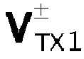
output terminals 


- The hybrid insertion loss for the transmit signal is thus given by:

- In order to get a low insertion loss for the transmit signal, one has to select a relatively small value for C3 for |Z4| >> |Z1| and |α| ≃ 1.
- As depicted in
fig. 3A , let i1 and i3 denote the currents entering the first input terminals of theadders adders - As the circuit is fully balanced, we have opposite currents circulating in the symmetric counterpart branches of the circuit, and:

- In order to get adequate echo suppression, the following relation shall hold:

- With regard to eq. (12), we then have:

- We further have:


- Applying Kirchoff's current law to the node





- If we equate the real and imaginary parts of eq. (19) with the real and imaginary parts of 1/Z 1, then the following two relations shall be adhered to for adequate echo suppression:


- There is seen in
fig. 3B the various impedances loading the transmission line when a far-end signal is being received through theline terminals - The line is modeled as two opposite-polarity ideal voltage generators


- Still assuming that the inverting terminals of the op-
amp transmission line 40 is loaded with a total impedance Z RX given by:
- Let


line terminals output terminals 


- The differential receive voltages at the receive
input terminal 

- For optimal power transfer from the transmission line into the receiver and minimal signal reflection at the line terminals, the resistance value of the matching resistor R1 is determined so as the real part of the input impedance Z RX matches the real part of the characteristic impedance Z C of the transmission line. If the impedance values C1, C2 and C3 are chosen sufficiently small for the input currents i1 to i4 to be low enough with respect to the main load current iL (assumption valid at low/mid-frequencies at least), then this requirement translates into:

- The reactance value of the capacitor C1 shall substantially match the difference between the reactance value of the first input branch of one adder and the reactance value of the second input branch of the other adder, namely 1/C2 - 1/C3, so as there are antiphase input currents at the common terminal of the adders.
- As aforementioned, the capacitance value of the capacitor C3 shall be chosen sufficiently small in order to have the lowest insertion loss for the transmit signal. In addition, the chosen capacitance value shall substantially match eq. (21), which is possible as eq. (20) and (21) leave some degree of freedom for selecting a capacitance value for the capacitor C2.
- The capacitance value of the capacitor C4 determines the receive gain across the
opamps - The capacitance value of the capacitor C5 determines the insertion gain of the echo cancellation voltage

- For instance, the following values can be used with a load resistance RL = 75Q (coaxial cable), a generator output resistance R0 = 22Q, and 1:1 as winding ratio for the line transformer:
- R1 = 26,5Q;
- C3 = 1pF;
- C2 = 0,5858pF;
- C1 = 1,414pF.
- The resistor R1 can be replaced by a tunable resistor. This allows to calibrate R1 by a limited amount so as to compensate for uncertainties or deviations on the line driver output impedance Z0 or on the average line characteristic impedance ZC. Thanks to the integration with the digital backend, this calibration can be done automatically.
- For instance, the variable resistor can be implemented as a MOSFET in the linear region in parallel with another resistor. The gate voltage on the MOSFET determines the resistance between its source and drain. Capacitors are added between the body and the source, and between the source and the gate, of the MOSFET to prevent large voltages in AC across the MOSFET terminals.
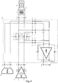
- There is seen in
fig. 4 a second alternative embodiment of the hybrid 100. - This embodiment differs from the first embodiment in that the two
adders LNA 23 for reduced cost and size. - The common terminals of the adders are coupled to the input terminals of the
LNA 23, and the output terminals of the adders are coupled to the respective opposite-polarity output terminals of theLNA 23. Presently, thecommon terminal 115 of thefirst adder 110 is coupled to the non-inverting input terminal of theLNA 23, and theoutput terminal 114 of thefirst adder 110 is coupled to the inverting output terminal of theLNA 23, and as feedback loop to thecommon terminal 115 of thefirst adder 110 through the capacitor C4. Symmetrically, thecommon terminal 125 of thesecond adder 120 is coupled to the inverting input terminal of theLNA 23, and theoutput terminal 124 of thesecond adder 120 is coupled to the non-inverting output terminal of theLNA 23, and as feedback loop to thecommon terminal 125 of thesecond adder 120 through the capacitor C4. - The remainder of the
transmission arrangement 100 is left unmodified. - The proposed transmission arrangement has a smaller footprint, and can be integrated within an IC. The capacitance values needed are compatible with the newest CMOS processes. In fact, smaller capacitors are beneficial since they allow more wideband operation. Furthermore, implementing small capacitor values is more accurate on an IC than in discrete components on a board.
- There is seen in
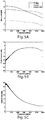
fig. 5A to 5C various performance plots for a hybrid as per the present invention. -
Fig. 5A represents the various insertion gains through the capacitive hybrid versus frequency. The transmit insertion gain from the DAC output ports up to the line terminals, and including the line driver gain, is depicted as a plain-line curve (TX-line). The receive insertion gain from the line terminals up to the ADC input ports, and including the LNA gain, is depicted as a dashed-line curve (line-RX). And last, the insertion gain of the additional echo cancellation signal from the output ports of the additional DAC up to the ADC input ports is depicted as a dotted-line curve (ECDAC-RX). As one can see, the frequency response of the hybrid is relatively flat across the 1 GHz frequency range. -
Fig. 5B plot represents the Trans-Hybrid Return Loss (THRL) versus frequency, that is to say the isolation gain from the DAC output ports up to the near-end ADC input ports, including both the line driver gain and the LNA gain. -
Fig. 5C plot represents the Figure of Merit (FOM), which is a more representative metric for the hybrid than the THRL. The mean FOM is about 21 dB, which a very good performance figure for such a wide frequency range (up to 1,2 GHz). - The FOM is computed from the gains TX-line and line-RX and from the THRL as follows (with gains expressed in dB):


- FOM is then given by:

- For instance at low frequencies, and based upon the plots 5A and 5B, FOM ≃ 11 + 8 - (-18) ≃ 37dB.
- Simulations of a resistive hybrid compared to a capacitive hybrid (with ideal amplifiers, meaning no noise generated inside the amplifiers) show that the resistive hybrid produces a noise PSD of -154dBm/Hz at the receiver input, while the proposed capacitive hybrid produces a noise PSD of only -167dBm/Hz. In the resistive hybrid, the resistors in the input branches and the feedback loop dominate the noise contribution. The noise contribution of the matching resistor R1, which is also present in the capacitive hybrid, is far lower. If the ADC noise floor is about -140dBm/Hz, the addition of a noise PSD of -154dBm/Hz results in an increase of 0,17dB of the noise PSD. However, if an LNA with a gain of 10dB is used after the resistive hybrid, the increase in the noise PSD is 1,46dB, which is rather substantial. With the proposed capacitive hybrid, and still assuming an LNA gain of 10dB, the increase in the noise PSD is only 0,09dB.
- Although the above embodiments mostly focus on wired transmissions, the present invention is similarly applicable to wireless full-duplex transmission. In this case, the transmitter output and the receiver input are coupled through the proposed
transmission arrangement 100 to a transmission medium, typically a coaxial cable, carrying the transmit and receive voltages to/from one or more antennas for EM propagation over the air. The transceiver typically accommodates additional circuitries such as up-down frequency mixer, further MIMO signal processing for path diversity, etc. Thetransmission arrangement 100 would then form part of a wireless base station or access point, or of a wireless user terminal, such as a smart phone, a laptop, and so forth. - It is to be noticed that the term 'comprising' should not be interpreted as being restricted to the means listed thereafter. Thus, the scope of the expression 'a device comprising means A and B' should not be limited to devices consisting only of components A and B. It means that with respect to the present invention, the relevant components of the device are A and B.
- It is to be further noticed that the term 'coupled' should not be interpreted as being restricted to direct connections only. Thus, the scope of the expression 'a device A coupled to a device B' should not be limited to devices or systems wherein an output of device A is directly connected to an input of device B, and/or vice-versa. It means that there exists a path between an output of A and an input of B, and/or vice-versa, which may be a path including other devices or means.
- The description and drawings merely illustrate the principles of the invention. It will thus be appreciated that those skilled in the art will be able to devise various arrangements that, although not explicitly described or shown herein, embody the principles of the invention. Furthermore, all examples recited herein are principally intended expressly to be only for pedagogical purposes to aid the reader in understanding the principles of the invention and the concepts contributed by the inventor(s) to furthering the art, and are to be construed as being without limitation to such specifically recited examples and conditions. Moreover, all statements herein reciting principles, aspects, and embodiments of the invention, as well as specific examples thereof, are intended to encompass equivalents thereof.
Claims (14)
- A transmission arrangement (100) for coupling a pair of transmit output terminals (101, 102) to a pair of medium terminals (103, 104) coupled a transmission medium (40), and the pair of medium terminals to a pair of receive input terminals (105, 106), the pairs of transmit output terminals, receive input terminals and medium terminals carrying opposite-polarity signals (±VTX; ±VRX; ±VLINE),
wherein the transmission arrangement comprises a first adder (110) and a second adder (120) with respective first and second adder input terminals (111, 121; 112, 122) and respective adder output terminals (114; 124),
wherein the pair of transmit output terminals is coupled to the pair of first adder input terminals, and is further coupled through respective first impedances (Z1) to the pair of second adder input terminals and to the pair of medium terminals, with the first and second adder input terminals being respectively coupled to opposite-polarity transmit output terminals, and the pair of receive input terminals is coupled to the pair of adder output terminals,
wherein the first impedances individually comprise a first resistor (R1) coupled in parallel with a first capacitor (C1), wherein the first and second adders individually comprise second and third capacitors (C2, C3) between the respective first and second adder input terminals and a common terminal (115; 125), and a feedback network between the adder output terminal and the common terminal,
and wherein the first capacitors have a reactance value that matches the difference between the reactance values of the second and third capacitors. - A transmission arrangement (100) according to claim 1, wherein the first resistors are matching resistors whose resistance value is determined for an input impedance of the transmission arrangement to match a characteristic impedance of the transmission medium.
- A transmission arrangement (100) according to claim 2, wherein the transmission arrangement further comprises an adjustment circuit for dynamically adjusting the resistance value of the first resistors.
- A transmission arrangement (100) according to claim 1, wherein the first and second adders individually comprise, as feedback network, a fourth capacitor (C4) coupled between the adder output terminal and the common terminal.
- A transmission arrangement (100) according to claim 1, wherein the first and second adders further individually comprise a third adder input terminal (113; 123), and a fifth capacitor (C5) between the third adder input terminal and the common terminal,
and wherein a further pair of transmit output terminals (107, 108) configured to output a differential echo cancellation signal (±VE) is coupled to the pair of third adder input terminals. - A transmission arrangement (100) according to claim 1, wherein the first and second adders further individually comprise a high-gain differential amplifier (116; 126) with a pair of amplifier input terminals, the inverting terminal of which being coupled to the common terminal, and an amplifier output terminal coupled to the adder output terminal.
- A transmission arrangement (100) according to claim 1, wherein the first and second adders form part of a receiver differential amplifier (23) with a pair of amplifier input terminals coupled to the pair of common terminals, and a pair of amplifier output terminals coupled to the pair of adder output terminals.
- An integrated circuit comprising a transmission arrangement (100) according to any of claims 1 to 7.
- An access node comprising a transmission arrangement (100) according to any of claims 1 to 7.
- An access node according to claim 9, wherein the access node is a Cable Modem Termination System CMTS, and the transmission medium is a coaxial cable.
- An access node according to claim 9, wherein the access node is a Distribution Point Unit DPU, and the transmission medium is a twisted copper pair.
- An access node according to claim 9, wherein the access node is a Digital Subscriber Line Access Multiplexer DSLAM, and the transmission medium is a twisted copper pair.
- An access node according to claim 9, wherein the access node is a wireless base station, and the transmission medium is coupled to one or more antennas for signal transmission and reception over the air.
- A subscriber device comprising a transmission arrangement (100) according to any of claims 1 to 7.
Priority Applications (2)
| Application Number | Priority Date | Filing Date | Title |
|---|---|---|---|
| EP17158402.2A EP3367580B1 (en) | 2017-02-28 | 2017-02-28 | Transmission arrangement for full-duplex communication |
| PCT/EP2018/054656 WO2018158190A1 (en) | 2017-02-28 | 2018-02-26 | Transmission arrangement for full-duplex communication |
Applications Claiming Priority (1)
| Application Number | Priority Date | Filing Date | Title |
|---|---|---|---|
| EP17158402.2A EP3367580B1 (en) | 2017-02-28 | 2017-02-28 | Transmission arrangement for full-duplex communication |
Publications (2)
| Publication Number | Publication Date |
|---|---|
| EP3367580A1 true EP3367580A1 (en) | 2018-08-29 |
| EP3367580B1 EP3367580B1 (en) | 2019-08-28 |
Family
ID=58261491
Family Applications (1)
| Application Number | Title | Priority Date | Filing Date |
|---|---|---|---|
| EP17158402.2A Active EP3367580B1 (en) | 2017-02-28 | 2017-02-28 | Transmission arrangement for full-duplex communication |
Country Status (2)
| Country | Link |
|---|---|
| EP (1) | EP3367580B1 (en) |
| WO (1) | WO2018158190A1 (en) |
Cited By (1)
| Publication number | Priority date | Publication date | Assignee | Title |
|---|---|---|---|---|
| CN114499812A (en) * | 2020-11-12 | 2022-05-13 | 安华高科技股份有限公司 | Capacitive hybrid with PGA for full-duplex transceivers |
Families Citing this family (1)
| Publication number | Priority date | Publication date | Assignee | Title |
|---|---|---|---|---|
| CN111372262A (en) * | 2020-02-16 | 2020-07-03 | 山东华箭科工创新科技有限公司 | 5G remote communication relay equipment and communication method thereof |
Citations (2)
| Publication number | Priority date | Publication date | Assignee | Title |
|---|---|---|---|---|
| US20030142688A1 (en) * | 2002-01-31 | 2003-07-31 | Infineon Technologies North America Corp. | Power efficient line driver with high performance echo cancellation for 1000BASE-T |
| US20030169875A1 (en) * | 2002-03-07 | 2003-09-11 | Lsi Logic Corporation | On-chip compensation scheme for bridged tap lines in ADSL hybrid |
-
2017
- 2017-02-28 EP EP17158402.2A patent/EP3367580B1/en active Active
-
2018
- 2018-02-26 WO PCT/EP2018/054656 patent/WO2018158190A1/en not_active Ceased
Patent Citations (2)
| Publication number | Priority date | Publication date | Assignee | Title |
|---|---|---|---|---|
| US20030142688A1 (en) * | 2002-01-31 | 2003-07-31 | Infineon Technologies North America Corp. | Power efficient line driver with high performance echo cancellation for 1000BASE-T |
| US20030169875A1 (en) * | 2002-03-07 | 2003-09-11 | Lsi Logic Corporation | On-chip compensation scheme for bridged tap lines in ADSL hybrid |
Cited By (4)
| Publication number | Priority date | Publication date | Assignee | Title |
|---|---|---|---|---|
| CN114499812A (en) * | 2020-11-12 | 2022-05-13 | 安华高科技股份有限公司 | Capacitive hybrid with PGA for full-duplex transceivers |
| EP4002705A1 (en) * | 2020-11-12 | 2022-05-25 | Avago Technologies International Sales Pte. Limited | Capacitive hybrid with pga for full duplex transceivers |
| US12058083B2 (en) | 2020-11-12 | 2024-08-06 | Avago Technologies International Sales Pte. Limited | Capacitive hybrid with PGA for full duplex transceivers |
| US12438688B2 (en) | 2020-11-12 | 2025-10-07 | Avago Technologies International Sales Pte. Limited | Capacitive hybrid with PGA for full duplex transceivers |
Also Published As
| Publication number | Publication date |
|---|---|
| EP3367580B1 (en) | 2019-08-28 |
| WO2018158190A1 (en) | 2018-09-07 |
Similar Documents
| Publication | Publication Date | Title |
|---|---|---|
| US11424785B2 (en) | Targeted rectangular conditioning | |
| US10200167B2 (en) | Full-duplex communication over a shared transmission medium | |
| US9160381B2 (en) | Adaptive frequency-domain reference noise canceller for multicarrier communications systems | |
| US9020145B2 (en) | MIMO mechanism for strong FEXT mitigation | |
| EP3654539B1 (en) | Cable modem and digital compensation for switchable analog filter to assist echo cancellation in full duplex cable modem | |
| CN101262253B (en) | Method for solving cross-interference issue in digital user line and cross-interference elimination device | |
| US9917617B2 (en) | Randomization of crosstalk probing signals | |
| WO2015135870A1 (en) | Non-linear precoder with separate tracking | |
| US11489654B2 (en) | Apparatus and method for full-duplex communication over a shared transmission medium | |
| WO2013041328A1 (en) | Power adaptation avoidance during crosstalk measurements | |
| US10432350B2 (en) | Method for adjusting parameters of sending device and receiving device, and terminal device | |
| EP3367580B1 (en) | Transmission arrangement for full-duplex communication | |
| Fouladifard et al. | On adaptive cancellation of IQ mismatch in OFDM receivers | |
| EP3306825A1 (en) | Two-step initialization procedure for adaptive analog echo cancellation | |
| CN112398507B (en) | Noise signal processing device and method | |
| JP6114412B2 (en) | Error feedback using detected constellation points |
Legal Events
| Date | Code | Title | Description |
|---|---|---|---|
| PUAI | Public reference made under article 153(3) epc to a published international application that has entered the european phase |
Free format text: ORIGINAL CODE: 0009012 |
|
| STAA | Information on the status of an ep patent application or granted ep patent |
Free format text: STATUS: THE APPLICATION HAS BEEN PUBLISHED |
|
| AK | Designated contracting states |
Kind code of ref document: A1 Designated state(s): AL AT BE BG CH CY CZ DE DK EE ES FI FR GB GR HR HU IE IS IT LI LT LU LV MC MK MT NL NO PL PT RO RS SE SI SK SM TR |
|
| AX | Request for extension of the european patent |
Extension state: BA ME |
|
| STAA | Information on the status of an ep patent application or granted ep patent |
Free format text: STATUS: REQUEST FOR EXAMINATION WAS MADE |
|
| GRAP | Despatch of communication of intention to grant a patent |
Free format text: ORIGINAL CODE: EPIDOSNIGR1 |
|
| STAA | Information on the status of an ep patent application or granted ep patent |
Free format text: STATUS: GRANT OF PATENT IS INTENDED |
|
| 17P | Request for examination filed |
Effective date: 20190228 |
|
| RBV | Designated contracting states (corrected) |
Designated state(s): AL AT BE BG CH CY CZ DE DK EE ES FI FR GB GR HR HU IE IS IT LI LT LU LV MC MK MT NL NO PL PT RO RS SE SI SK SM TR |
|
| INTG | Intention to grant announced |
Effective date: 20190410 |
|
| GRAS | Grant fee paid |
Free format text: ORIGINAL CODE: EPIDOSNIGR3 |
|
| GRAA | (expected) grant |
Free format text: ORIGINAL CODE: 0009210 |
|
| STAA | Information on the status of an ep patent application or granted ep patent |
Free format text: STATUS: THE PATENT HAS BEEN GRANTED |
|
| AK | Designated contracting states |
Kind code of ref document: B1 Designated state(s): AL AT BE BG CH CY CZ DE DK EE ES FI FR GB GR HR HU IE IS IT LI LT LU LV MC MK MT NL NO PL PT RO RS SE SI SK SM TR |
|
| REG | Reference to a national code |
Ref country code: GB Ref legal event code: FG4D |
|
| REG | Reference to a national code |
Ref country code: CH Ref legal event code: EP |
|
| RAP2 | Party data changed (patent owner data changed or rights of a patent transferred) |
Owner name: NOKIA SOLUTIONS AND NETWORKS OY |
|
| REG | Reference to a national code |
Ref country code: AT Ref legal event code: REF Ref document number: 1173688 Country of ref document: AT Kind code of ref document: T Effective date: 20190915 |
|
| REG | Reference to a national code |
Ref country code: IE Ref legal event code: FG4D |
|
| REG | Reference to a national code |
Ref country code: DE Ref legal event code: R096 Ref document number: 602017006426 Country of ref document: DE |
|
| REG | Reference to a national code |
Ref country code: NL Ref legal event code: MP Effective date: 20190828 |
|
| REG | Reference to a national code |
Ref country code: LT Ref legal event code: MG4D |
|
| PG25 | Lapsed in a contracting state [announced via postgrant information from national office to epo] |
Ref country code: FI Free format text: LAPSE BECAUSE OF FAILURE TO SUBMIT A TRANSLATION OF THE DESCRIPTION OR TO PAY THE FEE WITHIN THE PRESCRIBED TIME-LIMIT Effective date: 20190828 Ref country code: HR Free format text: LAPSE BECAUSE OF FAILURE TO SUBMIT A TRANSLATION OF THE DESCRIPTION OR TO PAY THE FEE WITHIN THE PRESCRIBED TIME-LIMIT Effective date: 20190828 Ref country code: BG Free format text: LAPSE BECAUSE OF FAILURE TO SUBMIT A TRANSLATION OF THE DESCRIPTION OR TO PAY THE FEE WITHIN THE PRESCRIBED TIME-LIMIT Effective date: 20191128 Ref country code: SE Free format text: LAPSE BECAUSE OF FAILURE TO SUBMIT A TRANSLATION OF THE DESCRIPTION OR TO PAY THE FEE WITHIN THE PRESCRIBED TIME-LIMIT Effective date: 20190828 Ref country code: NL Free format text: LAPSE BECAUSE OF FAILURE TO SUBMIT A TRANSLATION OF THE DESCRIPTION OR TO PAY THE FEE WITHIN THE PRESCRIBED TIME-LIMIT Effective date: 20190828 Ref country code: NO Free format text: LAPSE BECAUSE OF FAILURE TO SUBMIT A TRANSLATION OF THE DESCRIPTION OR TO PAY THE FEE WITHIN THE PRESCRIBED TIME-LIMIT Effective date: 20191128 Ref country code: LT Free format text: LAPSE BECAUSE OF FAILURE TO SUBMIT A TRANSLATION OF THE DESCRIPTION OR TO PAY THE FEE WITHIN THE PRESCRIBED TIME-LIMIT Effective date: 20190828 Ref country code: PT Free format text: LAPSE BECAUSE OF FAILURE TO SUBMIT A TRANSLATION OF THE DESCRIPTION OR TO PAY THE FEE WITHIN THE PRESCRIBED TIME-LIMIT Effective date: 20191230 |
|
| PG25 | Lapsed in a contracting state [announced via postgrant information from national office to epo] |
Ref country code: ES Free format text: LAPSE BECAUSE OF FAILURE TO SUBMIT A TRANSLATION OF THE DESCRIPTION OR TO PAY THE FEE WITHIN THE PRESCRIBED TIME-LIMIT Effective date: 20190828 Ref country code: GR Free format text: LAPSE BECAUSE OF FAILURE TO SUBMIT A TRANSLATION OF THE DESCRIPTION OR TO PAY THE FEE WITHIN THE PRESCRIBED TIME-LIMIT Effective date: 20191129 Ref country code: AL Free format text: LAPSE BECAUSE OF FAILURE TO SUBMIT A TRANSLATION OF THE DESCRIPTION OR TO PAY THE FEE WITHIN THE PRESCRIBED TIME-LIMIT Effective date: 20190828 Ref country code: LV Free format text: LAPSE BECAUSE OF FAILURE TO SUBMIT A TRANSLATION OF THE DESCRIPTION OR TO PAY THE FEE WITHIN THE PRESCRIBED TIME-LIMIT Effective date: 20190828 Ref country code: IS Free format text: LAPSE BECAUSE OF FAILURE TO SUBMIT A TRANSLATION OF THE DESCRIPTION OR TO PAY THE FEE WITHIN THE PRESCRIBED TIME-LIMIT Effective date: 20191228 Ref country code: RS Free format text: LAPSE BECAUSE OF FAILURE TO SUBMIT A TRANSLATION OF THE DESCRIPTION OR TO PAY THE FEE WITHIN THE PRESCRIBED TIME-LIMIT Effective date: 20190828 |
|
| REG | Reference to a national code |
Ref country code: AT Ref legal event code: MK05 Ref document number: 1173688 Country of ref document: AT Kind code of ref document: T Effective date: 20190828 |
|
| PG25 | Lapsed in a contracting state [announced via postgrant information from national office to epo] |
Ref country code: TR Free format text: LAPSE BECAUSE OF FAILURE TO SUBMIT A TRANSLATION OF THE DESCRIPTION OR TO PAY THE FEE WITHIN THE PRESCRIBED TIME-LIMIT Effective date: 20190828 |
|
| PG25 | Lapsed in a contracting state [announced via postgrant information from national office to epo] |
Ref country code: IT Free format text: LAPSE BECAUSE OF FAILURE TO SUBMIT A TRANSLATION OF THE DESCRIPTION OR TO PAY THE FEE WITHIN THE PRESCRIBED TIME-LIMIT Effective date: 20190828 Ref country code: PL Free format text: LAPSE BECAUSE OF FAILURE TO SUBMIT A TRANSLATION OF THE DESCRIPTION OR TO PAY THE FEE WITHIN THE PRESCRIBED TIME-LIMIT Effective date: 20190828 Ref country code: EE Free format text: LAPSE BECAUSE OF FAILURE TO SUBMIT A TRANSLATION OF THE DESCRIPTION OR TO PAY THE FEE WITHIN THE PRESCRIBED TIME-LIMIT Effective date: 20190828 Ref country code: RO Free format text: LAPSE BECAUSE OF FAILURE TO SUBMIT A TRANSLATION OF THE DESCRIPTION OR TO PAY THE FEE WITHIN THE PRESCRIBED TIME-LIMIT Effective date: 20190828 Ref country code: AT Free format text: LAPSE BECAUSE OF FAILURE TO SUBMIT A TRANSLATION OF THE DESCRIPTION OR TO PAY THE FEE WITHIN THE PRESCRIBED TIME-LIMIT Effective date: 20190828 Ref country code: DK Free format text: LAPSE BECAUSE OF FAILURE TO SUBMIT A TRANSLATION OF THE DESCRIPTION OR TO PAY THE FEE WITHIN THE PRESCRIBED TIME-LIMIT Effective date: 20190828 |
|
| PG25 | Lapsed in a contracting state [announced via postgrant information from national office to epo] |
Ref country code: CZ Free format text: LAPSE BECAUSE OF FAILURE TO SUBMIT A TRANSLATION OF THE DESCRIPTION OR TO PAY THE FEE WITHIN THE PRESCRIBED TIME-LIMIT Effective date: 20190828 Ref country code: SK Free format text: LAPSE BECAUSE OF FAILURE TO SUBMIT A TRANSLATION OF THE DESCRIPTION OR TO PAY THE FEE WITHIN THE PRESCRIBED TIME-LIMIT Effective date: 20190828 Ref country code: SM Free format text: LAPSE BECAUSE OF FAILURE TO SUBMIT A TRANSLATION OF THE DESCRIPTION OR TO PAY THE FEE WITHIN THE PRESCRIBED TIME-LIMIT Effective date: 20190828 Ref country code: IS Free format text: LAPSE BECAUSE OF FAILURE TO SUBMIT A TRANSLATION OF THE DESCRIPTION OR TO PAY THE FEE WITHIN THE PRESCRIBED TIME-LIMIT Effective date: 20200224 |
|
| REG | Reference to a national code |
Ref country code: DE Ref legal event code: R097 Ref document number: 602017006426 Country of ref document: DE |
|
| PLBE | No opposition filed within time limit |
Free format text: ORIGINAL CODE: 0009261 |
|
| STAA | Information on the status of an ep patent application or granted ep patent |
Free format text: STATUS: NO OPPOSITION FILED WITHIN TIME LIMIT |
|
| PG2D | Information on lapse in contracting state deleted |
Ref country code: IS |
|
| 26N | No opposition filed |
Effective date: 20200603 |
|
| PG25 | Lapsed in a contracting state [announced via postgrant information from national office to epo] |
Ref country code: SI Free format text: LAPSE BECAUSE OF FAILURE TO SUBMIT A TRANSLATION OF THE DESCRIPTION OR TO PAY THE FEE WITHIN THE PRESCRIBED TIME-LIMIT Effective date: 20190828 |
|
| REG | Reference to a national code |
Ref country code: CH Ref legal event code: PL |
|
| REG | Reference to a national code |
Ref country code: BE Ref legal event code: MM Effective date: 20200229 |
|
| PG25 | Lapsed in a contracting state [announced via postgrant information from national office to epo] |
Ref country code: LU Free format text: LAPSE BECAUSE OF NON-PAYMENT OF DUE FEES Effective date: 20200228 Ref country code: MC Free format text: LAPSE BECAUSE OF FAILURE TO SUBMIT A TRANSLATION OF THE DESCRIPTION OR TO PAY THE FEE WITHIN THE PRESCRIBED TIME-LIMIT Effective date: 20190828 |
|
| PG25 | Lapsed in a contracting state [announced via postgrant information from national office to epo] |
Ref country code: LI Free format text: LAPSE BECAUSE OF NON-PAYMENT OF DUE FEES Effective date: 20200229 Ref country code: CH Free format text: LAPSE BECAUSE OF NON-PAYMENT OF DUE FEES Effective date: 20200229 |
|
| PG25 | Lapsed in a contracting state [announced via postgrant information from national office to epo] |
Ref country code: IE Free format text: LAPSE BECAUSE OF NON-PAYMENT OF DUE FEES Effective date: 20200228 |
|
| PG25 | Lapsed in a contracting state [announced via postgrant information from national office to epo] |
Ref country code: BE Free format text: LAPSE BECAUSE OF NON-PAYMENT OF DUE FEES Effective date: 20200229 |
|
| PG25 | Lapsed in a contracting state [announced via postgrant information from national office to epo] |
Ref country code: MT Free format text: LAPSE BECAUSE OF FAILURE TO SUBMIT A TRANSLATION OF THE DESCRIPTION OR TO PAY THE FEE WITHIN THE PRESCRIBED TIME-LIMIT Effective date: 20190828 Ref country code: CY Free format text: LAPSE BECAUSE OF FAILURE TO SUBMIT A TRANSLATION OF THE DESCRIPTION OR TO PAY THE FEE WITHIN THE PRESCRIBED TIME-LIMIT Effective date: 20190828 |
|
| PG25 | Lapsed in a contracting state [announced via postgrant information from national office to epo] |
Ref country code: MK Free format text: LAPSE BECAUSE OF FAILURE TO SUBMIT A TRANSLATION OF THE DESCRIPTION OR TO PAY THE FEE WITHIN THE PRESCRIBED TIME-LIMIT Effective date: 20190828 |
|
| PGFP | Annual fee paid to national office [announced via postgrant information from national office to epo] |
Ref country code: FR Payment date: 20251231 Year of fee payment: 10 |
|
| PGFP | Annual fee paid to national office [announced via postgrant information from national office to epo] |
Ref country code: GB Payment date: 20260106 Year of fee payment: 10 |
|
| PGFP | Annual fee paid to national office [announced via postgrant information from national office to epo] |
Ref country code: DE Payment date: 20260102 Year of fee payment: 10 |