EP3367573A1 - Delta-sigma analog-to-digital converter - Google Patents
Delta-sigma analog-to-digital converter Download PDFInfo
- Publication number
- EP3367573A1 EP3367573A1 EP17158444.4A EP17158444A EP3367573A1 EP 3367573 A1 EP3367573 A1 EP 3367573A1 EP 17158444 A EP17158444 A EP 17158444A EP 3367573 A1 EP3367573 A1 EP 3367573A1
- Authority
- EP
- European Patent Office
- Prior art keywords
- sample
- time
- analog
- sigma
- output
- Prior art date
- Legal status (The legal status is an assumption and is not a legal conclusion. Google has not performed a legal analysis and makes no representation as to the accuracy of the status listed.)
- Granted
Links
Images



Classifications
-
- H—ELECTRICITY
- H03—ELECTRONIC CIRCUITRY
- H03M—CODING; DECODING; CODE CONVERSION IN GENERAL
- H03M3/00—Conversion of analogue values to or from differential modulation
- H03M3/30—Delta-sigma modulation
- H03M3/32—Delta-sigma modulation with special provisions or arrangements for power saving, e.g. by allowing a sleep mode, using lower supply voltage for downstream stages, using multiple clock domains, by selectively turning on stages when needed
-
- H—ELECTRICITY
- H03—ELECTRONIC CIRCUITRY
- H03M—CODING; DECODING; CODE CONVERSION IN GENERAL
- H03M3/00—Conversion of analogue values to or from differential modulation
- H03M3/30—Delta-sigma modulation
- H03M3/458—Analogue/digital converters using delta-sigma modulation as an intermediate step
-
- Y—GENERAL TAGGING OF NEW TECHNOLOGICAL DEVELOPMENTS; GENERAL TAGGING OF CROSS-SECTIONAL TECHNOLOGIES SPANNING OVER SEVERAL SECTIONS OF THE IPC; TECHNICAL SUBJECTS COVERED BY FORMER USPC CROSS-REFERENCE ART COLLECTIONS [XRACs] AND DIGESTS
- Y02—TECHNOLOGIES OR APPLICATIONS FOR MITIGATION OR ADAPTATION AGAINST CLIMATE CHANGE
- Y02D—CLIMATE CHANGE MITIGATION TECHNOLOGIES IN INFORMATION AND COMMUNICATION TECHNOLOGIES [ICT], I.E. INFORMATION AND COMMUNICATION TECHNOLOGIES AIMING AT THE REDUCTION OF THEIR OWN ENERGY USE
- Y02D30/00—Reducing energy consumption in communication networks
- Y02D30/70—Reducing energy consumption in communication networks in wireless communication networks
Definitions
- the invention relates to an analog-to-digital converter using a sigma-delta modulator.
- Sigma-delta analog-to-digital converters operate at significant oversampling and employ digital decimation filters to deliver a signal at the required sample rate.
- the decimation filter comprises multiple decimation states, e.g., using so-called cascaded integrator comb (CIC) filters, delivering samples spaced equidistantly in time.
- CIC cascaded integrator comb
- a so-called cyclic prefix is used and inserted into the OFDM symbol in order to obtain a time window of orthogonal data transmission without inter-carrier and inter-symbol interference.
- a cyclic prefix is a guard band that is made between the LTE symbols.
- the downlink signal format definition for LTE and also narrow-band LTE is compatible to a sampling frequency of 1920 kHz.
- the so-called "normal cyclic prefix" has a duration of either 9 or 10 samples, respectively for certain OFDM symbols.
- Lower sampling frequencies result in a fractional sample spacing.
- Standard multi-mode receivers for LTE Cat-M and narrow-band LTE would operate at 1920 kHz in both modes and use a partial FFT in case of narrowband LTE operation, which is suboptimum with respect to power efficiency.
- the narrowband LTE downlink signal utilizes a bandwidth of 180 kHz. Using a sampling frequency as low as 240 kHz it is desirable to achieve a low power consumption. However, when using equidistant sampling at this rate, the cyclic prefixes have non-integer sample durations.
- a crystal oscillator without voltage control achieves better phase noise performance compared to a controllable counterpart, which is desirable when targeting the highest coverage class, where operation at very low signal-to-noise-ration (SNR) requires coherent combining across long signal durations.
- Coverage classes are defined for different maximum supported signal attenuation between transmitter and receiver.
- the highest coverage class is the one supporting 164 dB of attenuation between base station and user equipment antennas.
- the sampling frequency can no longer be locked to the radio frequency.
- Some means of fractional resampling helps to lock the sampling clock to the carrier frequency.
- Such means is for example a fractional re-sampler consisting of a polyphase filter and a linear interpolator.
- an analog-to-digital converter comprising a sigma-delta modulator and a sample-time-counter, both controlled by a sample clock a next-sample-time computation unit configured to compute a sample-time-counter value when a next digital output sample is requested, a sample-computation-trigger unit connected to the next-sample-time computation unit configured to compare an actual sample-time-counter value with the sample-time-counter value when the next digital output sample is requested and to trigger a computation unit for calculating a next digital sample when requested and by powering off the sigma-delta modulator in intervals where its delivered samples are not used for any computed decimator output sample.
- the computation unit comprises an output-compute-counter unit, a sample buffer and an output-sample accumulator, whereas the output-compute-counter unit (8) and output-sample accumulator (9) are triggered in dependence of a difference between the actual sample-time-counter value and the next sample-time-counter value, whereas the output-sample accumulator is configured to compute digital output samples in dependence of a read filter impulse response sample by sample from a filter coefficient memory and an accumulation of said samples after multiplication with the related digital output value of the sigma-delta modulator read from the sample buffer at certain values of the sample-time-counter.
- a sigma-delta modulator power control unit powers on or off the sigma-delta modulator according to a next digital sample request.
- an RF power control unit powers on or off the RF receiver chain or part of the RF receiver chain according to a next digital sample request.
- a part of the receiver chain could be a low noise amplifier (LNA), a mixer, a local oscillator (LO) comprising a phase-locked-loop (PLL) or a variable gain amplifier (VGA), all of them or only parts or single components of the receiver chain can be powered on or off.
- LNA low noise amplifier
- LO local oscillator
- PLL phase-locked-loop
- VGA variable gain amplifier
- the decimation is split into a pre-decimation followed by the decimation method described above.
- the proposed analog-to-digital converter comprises the following: A one-step decimation from the high sigma-delta modulator output sampling frequency to the receiver input sampling frequency should be performed. Thus, each output sample is computed as a weighted sum over a range of input samples, corresponding to the filter length.
- the choice of the sigma-delta modulator sampling frequency should be a sufficiently large multiple of all supported receiver input sample frequencies, such that a sufficiently large output signal-to-noise ratio (SNR) by means of noise shaping and subsequent (one-step decimation) filtering will be achieved.
- SNR signal-to-noise ratio
- the receiver would request filtered samples either equidistantly spaced, e.g., one output sample every K input samples or non-equidistantly spaced, e.g., when inserting a time gap to discard the OFDM cyclic prefix. So, there is a possibility to select the time position for decimator output sample computation at time granularity of the much higher input sample frequency. There are also means to determine time intervals where no input sample to the decimator is needed, and further controlling means to power off the sigma-delta modulator circuitry.
- a sample-computation-trigger unit is such a mean that is connected to the next-sample-time-computation unit configured to compare an actual sample-time-counter value with the sample-time-counter value when the next digital output sample is requested, whereas the sample-computation-trigger unit triggers a sigma-delta modulator power control unit, an output-compute-counter unit as well as an output-sample accumulator in dependence of a difference between the actual sample-time-counter value and the next sample-time-counter value.
- Background is that around each decimator output sample, a number of input samples must be available to support the length of the decimation filter.
- a power switch is controlled by the result of comparing a sample-time-counter operating at the high rate against the time window required to compute an output sample (filter response duration plus sigma delta modulator settling time). As long as the time distance from sample to sample is shorter than the time window duration, the switch will keep the circuitry powered on. Furthermore, there are means to artificially move the point of time of output sample computation by +/-1 input sample of time, in order to tune the output sampling frequency to compensate for sample frequency offset.
- the background is that an equidistant sampling at a spacing of K input samples produces a fixed sampling rate. By duplicating one input sample every N output samples, the average sample spacing decreases from "every K input samples" to "every K-(1/K/N)".
- the average sample spacing increases from "every K input samples” to "every K+(1/K/N)".
- the means to achieve this is a sample counter and the possibility to either skip or duplicate an input sample.
- the circuitry has to be implemented once in a decimator for complex in-phase (I) and quadrature phase (Q) signals, and for the case of multiple receive antennas.
- sample computation path consisting of the sigma-delta modulator, sample buffer, sample multiplier and output sample accumulator.
- the sigma-delta modulator is a single-bit or a multi-bit and/or a continuous-time or discrete-time and/or a bandpass or baseband sigma-delta modulator.
- the type is selectable in dependence of the application.
- a sample clock controls the sigma-delta modulator and a sample-time-counter.
- the digital output values of the sigma-delta modulator are stored in a sample buffer, under control of the sample-time-counter.
- next-sample-time-computation unit is activated by a request format starting at time point t and consisting in delivering N samples of equidistant spacing T and time ticks of the sample clock.
- a sample computation request asks for digital output samples to be computed at certain values of the sample time counter by using a simple format of such a request that consists in delivering N samples of equidistant spacing T time ticks of the sample clock.
- More complex, implementation specific request formats are possible, e.g., to skip the cyclic prefix in OFDM, or to obtain a non-integer sampling frequency ratio.
- the next-sample-time-computation unit computes the sample time counter value when the next output sample is requested.
- the next sample time is the current sample time plus an offset K.
- a one-time larger offset e.g., NCP*K, may be used to skip the cyclic prefix, in which case the sigma-delta modulator may get powered off.
- the sample-computation-trigger unit serves two purposes, both based upon comparing the actual sample time counter value with the sample time counter value when the next sample is requested: If the delta of the two values falls below the filter length, it requests the sigma-delta modulator power Control to turn on the sigma-delta modulator, and if the values match, it triggers computation of the next output sample. So in a preferred embodiment the sample-computation-trigger unit powers on the sigma-delta modulator if the difference of the actual sample-time-counter value and the sample-time-counter value when the next digital output sample is requested falls below a filter length.
- sample-computation-trigger unit triggers the computation of the next digital output sample if the actual sample-time-counter value and the sample-time-counter value when the next digital output sample is requested matches.
- the sample-time-counter value is a current sampling time plus an offset K.
- a one-time larger offset is used to skip a portion of the signal, in which case the sigma-delta modulator is powered off.
- Multiple sample requests will be configured, supporting cases where the time delta between the last sample of request 0, t 0 +(K 0 -1)*T 0 , and the 1st sample of request 1, t 1 , is different from T 0 .
- request 1 may use a sample period T 1 which is distinct from T 0 .
- a shape of the filter is varied by a change of coefficients stored in the filter coefficient memory and a length of the filter.
- the proposed solution supports simple variation of the filter shape by change of coefficients and length of the filter itself.
- the proposed solution for power control of the sigma-delta modulator can also be extended further, beyond control of the sigma-delta modulator, e.g., to control a radio frequency mixer, low noise amplifier and further amplification stages. So it can be used in low power receivers, e.g., in modems for sensor networks or modems employing energy harvesting.
- the method uses an one-step decimation filtering from a high sigma-delta modulator output sampling frequency to a lower receiver input sampling frequency by computing weighted sums over ranges of input samples according to the filter length, whereas the output sample times and thus the associated ranges of input samples are determined as requested via configuration, N samples of equidistant spacing T starting at time t.
- a baseband receiver requests the filtered samples equidistantly spaced or non-equidistantly spaced, whereas the sigma-delta modulator as well as other components of the RF side can be powered off when no sample is requested in order to save energy and to reduce the overall power consumption.
- Figure 1 shows a timeline with on- and off- periods, whereas samples are requested in the on-period. In the off-period no samples are requested. In such off-periods it is possible to power off the sigma-delta modulator 1 and other components of the RF side, because they are not needed when no samples are requested. This results in saving energy and a reduction in the overall power consumption. With the inventive analog-to-digital converter it is possible to request output samples at any time, meaning at an arbitrary point in time whenever it is desired. An advantage is that this is not restricted to equidistant time positions as with standard A/D converters.
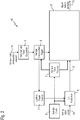
- Figure 2 shows an analog-to-digital converter 16 which receives a continuous-time analog signal 14 and delivers a discrete-time digital signal 13.
- a sample clock 3 controls the sigma-delta modulator 1 and a sample time counter 2.
- the samples are put out by the computation unit 17 whenever the comparison of the actual sample-time-counter value with the sample-time-counter value when the next sample is requested matches, meaning when the delta of the two values is zero. So, the sigma-delta modulator power control 7 turns on the sigma-delta modulator 1, if the delta of the two values falls below a filter length of the computation unit 17, and if the values match, it triggers the computation of the next output sample.
- Figure 3 shows the analog-to-digital converter 16 with a possible embodiment of the computation unit 17.
- Figure 3 shows an analog-to-digital converter 16 which receives a continuous-time analog signal 14 and delivers a discrete-time digital signal 13.
- a sample clock 3 controls the sigma-delta modulator 1 and a sample time counter 2.
- the sigma-delta modulator can be connected to an optional pre-decimation filter 18. Inserting a simple pre-decimation filter 18 allows minimizing the overall implementation complexity and power consumption of the decimation filter as a whole.
- the digital output values 12 of the sigma-delta modulator 1 are stored in a sample buffer 4, under control of the sample time counter 2.
- a sample computation request 15 asks for digital output samples 13 to be computed at certain values of the sample-time-counter 2.
- a simple format of such a request consists in delivering N samples of equidistant spacing T time ticks of the sample clock. More complex, implementation specific request formats are possible, e.g., to skip the cyclic prefix in OFDM, or to obtain a non-integer sampling frequency ratio.
- the next-sample-time-computation unit 5 computes the sample-time-counter value when the next output sample is requested. For equidistant sampling, the next sample time is the current sample time plus an offset K.
- a one-time larger offset e.g., NCP*K
- NCP*K a one-time larger offset
- the sample-computation-trigger unit 6 serves two purposes, both based upon comparing the actual sample-time-counter value with the sample-time-counter value when the next sample is requested: If the delta of the two values falls below the filter length, it requests the sigma-delta modulator power control 7 to turn on the sigma-delta modulator 1, and if the values match, it triggers computation of the next output sample.
- the actual output sample computation consists in reading the filter impulse response sample by sample from the filter coefficient memory 10 and accumulating 9 after multiplication 11 with the related sample value read from the buffer 4, given that each output sample is a weighted sum over a set of input samples stored in the sample buffer 4.
- the sigma-delta modulator 1 could be single-bit or multi-bit, continuous-time or discrete-time, baseband or bandpass sampling of any order.
- the proposed solution requires only a small amount of logic to implement the required functionality, it is able to perform the required functionality at very low power consumption, it offers versatile use, and it supports simple variation of the filter shape by change of coefficients and length of the computation unit 17.
- FIG. 4 shows another embodiment of the invention.
- the analog-to-digital converter can additionally comprise an optional RF path power control unit which is triggered by the sample-computation trigger unit 6 and is used to power on or off the entire RF receive path, or parts of the RF receive path.
Landscapes
- Engineering & Computer Science (AREA)
- Theoretical Computer Science (AREA)
- Compression, Expansion, Code Conversion, And Decoders (AREA)
Abstract
Description
- The invention relates to an analog-to-digital converter using a sigma-delta modulator.
- Sigma-delta analog-to-digital converters operate at significant oversampling and employ digital decimation filters to deliver a signal at the required sample rate. Typically, the decimation filter comprises multiple decimation states, e.g., using so-called cascaded integrator comb (CIC) filters, delivering samples spaced equidistantly in time.
- In wireless radio transmission it is common to operate at a fixed ratio between carrier frequency and sampling frequency. At the receiver this may be achieved by deriving both the carrier frequency clock as well as the sample clock from a common reference oscillator. Given that the carrier frequency value is known at the receiver, by tuning the carrier frequency offset to zero via reference oscillator frequency change, it is also possible to exactly meet the correct sampling frequency. This holds exactly in static scenarios without distance change between transmitter and receiver and typically good enough in mobile scenarios. Alternatively to tuning a common reference oscillator, a fractional re-sampler may take care of sampling frequency correction, which is a dedicated extra functional block.
- Furthermore, in baseband receivers for OFDM (Orthogonal Frequency-Division Multiplexing) reception the FFT (fast Fourier transformation) portions related to individual OFDM symbols would be cut out of the signal stream, typically leaving the entire signal processing prior to this point running, including analog-to-digital conversion (ADC) and related decimation filtering, which is mandatory for sigma-delta (SD) type of ADCs. In other words, samples of the discarded cyclic prefixes are actually computed beforehand, which might be regarded as a waste of energy. In the LTE standard a so-called cyclic prefix (CP) is used and inserted into the OFDM symbol in order to obtain a time window of orthogonal data transmission without inter-carrier and inter-symbol interference. Thus, a cyclic prefix is a guard band that is made between the LTE symbols.
- The downlink signal format definition for LTE and also narrow-band LTE is compatible to a sampling frequency of 1920 kHz. At this sampling frequency, the so-called "normal cyclic prefix" has a duration of either 9 or 10 samples, respectively for certain OFDM symbols. Lower sampling frequencies result in a fractional sample spacing. Standard multi-mode receivers for LTE Cat-M and narrow-band LTE would operate at 1920 kHz in both modes and use a partial FFT in case of narrowband LTE operation, which is suboptimum with respect to power efficiency.
- The narrowband LTE downlink signal utilizes a bandwidth of 180 kHz. Using a sampling frequency as low as 240 kHz it is desirable to achieve a low power consumption. However, when using equidistant sampling at this rate, the cyclic prefixes have non-integer sample durations.
- Therefore, it is desirable to have a simple decimation filter which can insert pauses of non-integer numbers of samples.
- So, it is desirable to save energy during time gaps when no received sample is needed.
- Although, a crystal oscillator without voltage control achieves better phase noise performance compared to a controllable counterpart, which is desirable when targeting the highest coverage class, where operation at very low signal-to-noise-ration (SNR) requires coherent combining across long signal durations. Coverage classes are defined for different maximum supported signal attenuation between transmitter and receiver. For example, the highest coverage class is the one supporting 164 dB of attenuation between base station and user equipment antennas. However, when using such type of oscillator, the sampling frequency can no longer be locked to the radio frequency. Some means of fractional resampling helps to lock the sampling clock to the carrier frequency. Such means is for example a fractional re-sampler consisting of a polyphase filter and a linear interpolator.
- So, a simple analog-to-digital converter that can realize and satisfy the above requirements is wanted.
- The objective of the invention will be solved by an analog-to-digital converter comprising a sigma-delta modulator and a sample-time-counter, both controlled by a sample clock a next-sample-time computation unit configured to compute a sample-time-counter value when a next digital output sample is requested, a sample-computation-trigger unit connected to the next-sample-time computation unit configured to compare an actual sample-time-counter value with the sample-time-counter value when the next digital output sample is requested and to trigger a computation unit for calculating a next digital sample when requested and by powering off the sigma-delta modulator in intervals where its delivered samples are not used for any computed decimator output sample.
- In a preferred embodiment of the invention the computation unit comprises an output-compute-counter unit, a sample buffer and an output-sample accumulator, whereas the output-compute-counter unit (8) and output-sample accumulator (9) are triggered in dependence of a difference between the actual sample-time-counter value and the next sample-time-counter value, whereas the output-sample accumulator is configured to compute digital output samples in dependence of a read filter impulse response sample by sample from a filter coefficient memory and an accumulation of said samples after multiplication with the related digital output value of the sigma-delta modulator read from the sample buffer at certain values of the sample-time-counter.
- And in another embodiment of the invention a sigma-delta modulator power control unit powers on or off the sigma-delta modulator according to a next digital sample request.
- In another further embodiment of the invention an RF power control unit powers on or off the RF receiver chain or part of the RF receiver chain according to a next digital sample request. A part of the receiver chain could be a low noise amplifier (LNA), a mixer, a local oscillator (LO) comprising a phase-locked-loop (PLL) or a variable gain amplifier (VGA), all of them or only parts or single components of the receiver chain can be powered on or off.
- And in another embodiment of the invention, the decimation is split into a pre-decimation followed by the decimation method described above.
- In other words, the proposed analog-to-digital converter comprises the following: A one-step decimation from the high sigma-delta modulator output sampling frequency to the receiver input sampling frequency should be performed. Thus, each output sample is computed as a weighted sum over a range of input samples, corresponding to the filter length. The choice of the sigma-delta modulator sampling frequency should be a sufficiently large multiple of all supported receiver input sample frequencies, such that a sufficiently large output signal-to-noise ratio (SNR) by means of noise shaping and subsequent (one-step decimation) filtering will be achieved. In a receiver application, the receiver would request filtered samples either equidistantly spaced, e.g., one output sample every K input samples or non-equidistantly spaced, e.g., when inserting a time gap to discard the OFDM cyclic prefix. So, there is a possibility to select the time position for decimator output sample computation at time granularity of the much higher input sample frequency. There are also means to determine time intervals where no input sample to the decimator is needed, and further controlling means to power off the sigma-delta modulator circuitry. A sample-computation-trigger unit is such a mean that is connected to the next-sample-time-computation unit configured to compare an actual sample-time-counter value with the sample-time-counter value when the next digital output sample is requested, whereas the sample-computation-trigger unit triggers a sigma-delta modulator power control unit, an output-compute-counter unit as well as an output-sample accumulator in dependence of a difference between the actual sample-time-counter value and the next sample-time-counter value. Background is that around each decimator output sample, a number of input samples must be available to support the length of the decimation filter. A power switch is controlled by the result of comparing a sample-time-counter operating at the high rate against the time window required to compute an output sample (filter response duration plus sigma delta modulator settling time). As long as the time distance from sample to sample is shorter than the time window duration, the switch will keep the circuitry powered on. Furthermore, there are means to artificially move the point of time of output sample computation by +/-1 input sample of time, in order to tune the output sampling frequency to compensate for sample frequency offset. The background is that an equidistant sampling at a spacing of K input samples produces a fixed sampling rate. By duplicating one input sample every N output samples, the average sample spacing decreases from "every K input samples" to "every K-(1/K/N)". Vice versa, by removing one input sample every N output samples, the average sample spacing increases from "every K input samples" to "every K+(1/K/N)". The means to achieve this is a sample counter and the possibility to either skip or duplicate an input sample. There is also a decimator control circuitry to request portions of equidistantly sampled output signal separated by arbitrarily selected time gaps. The circuitry has to be implemented once in a decimator for complex in-phase (I) and quadrature phase (Q) signals, and for the case of multiple receive antennas.
- All may be shared, except the sample computation path consisting of the sigma-delta modulator, sample buffer, sample multiplier and output sample accumulator. By this a very flexible and easily adapted solution achieves very low power consumption and small silicon area.
- In further embodiments of the invention the sigma-delta modulator is a single-bit or a multi-bit and/or a continuous-time or discrete-time and/or a bandpass or baseband sigma-delta modulator. The type is selectable in dependence of the application. A sample clock controls the sigma-delta modulator and a sample-time-counter. The digital output values of the sigma-delta modulator are stored in a sample buffer, under control of the sample-time-counter.
- In another embodiment the next-sample-time-computation unit is activated by a request format starting at time point t and consisting in delivering N samples of equidistant spacing T and time ticks of the sample clock. Meaning that a sample computation request asks for digital output samples to be computed at certain values of the sample time counter by using a simple format of such a request that consists in delivering N samples of equidistant spacing T time ticks of the sample clock. More complex, implementation specific request formats are possible, e.g., to skip the cyclic prefix in OFDM, or to obtain a non-integer sampling frequency ratio.
- The next-sample-time-computation unit computes the sample time counter value when the next output sample is requested. For equidistant sampling, the next sample time is the current sample time plus an offset K. In OFDM, a one-time larger offset, e.g., NCP*K, may be used to skip the cyclic prefix, in which case the sigma-delta modulator may get powered off.
- The sample-computation-trigger unit serves two purposes, both based upon comparing the actual sample time counter value with the sample time counter value when the next sample is requested: If the delta of the two values falls below the filter length, it requests the sigma-delta modulator power Control to turn on the sigma-delta modulator, and if the values match, it triggers computation of the next output sample. So in a preferred embodiment the sample-computation-trigger unit powers on the sigma-delta modulator if the difference of the actual sample-time-counter value and the sample-time-counter value when the next digital output sample is requested falls below a filter length.
- In another preferred embodiment the sample-computation-trigger unit triggers the computation of the next digital output sample if the actual sample-time-counter value and the sample-time-counter value when the next digital output sample is requested matches.
- In an embodiment of the invention the sample-time-counter value is a current sampling time plus an offset K.
- And in a preferred embodiment a one-time larger offset is used to skip a portion of the signal, in which case the sigma-delta modulator is powered off. Multiple sample requests will be configured, supporting cases where the time delta between the last sample of request 0, t0+(K0-1)*T0, and the 1st sample of
request 1, t1, is different from T0. - Also,
request 1 may use a sample period T1 which is distinct from T0. - In a further embodiment a shape of the filter is varied by a change of coefficients stored in the filter coefficient memory and a length of the filter. The proposed solution supports simple variation of the filter shape by change of coefficients and length of the filter itself.
- The proposed solution for power control of the sigma-delta modulator can also be extended further, beyond control of the sigma-delta modulator, e.g., to control a radio frequency mixer, low noise amplifier and further amplification stages. So it can be used in low power receivers, e.g., in modems for sensor networks or modems employing energy harvesting.
- The objective of the invention will be also solved by a method for converting an analog signal into a digital signal using the analog-to-digital converter according to
claims 1 to 10, wherein the method comprising the following steps: - using a sigma-delta modulator to produce a quantized, noise-shaped signal at a large sampling frequency,
- delivering output samples at requested output time positions by computing weighted sums over appropriate ranges of input samples according to the filter length,
- powering off the sigma-delta modulator when no filtered sample is requested in an off-period.
- With other words the method uses an one-step decimation filtering from a high sigma-delta modulator output sampling frequency to a lower receiver input sampling frequency by computing weighted sums over ranges of input samples according to the filter length, whereas the output sample times and thus the associated ranges of input samples are determined as requested via configuration, N samples of equidistant spacing T starting at time t.
- In a preferred embodiment of the inventive method a baseband receiver requests the filtered samples equidistantly spaced or non-equidistantly spaced, whereas the sigma-delta modulator as well as other components of the RF side can be powered off when no sample is requested in order to save energy and to reduce the overall power consumption.
- The invention will be explained in more detail using an exemplary embodiment.
- The appended drawing shows
- Fig. 1
- Schematical drawing of a timeline, with on-and off- periods and where samples are requested in the on-period and no samples are requested in the off-period;
- Fig. 2
- An analog-to digital converter with the inventive extension of the computation unit;
- Fig. 3
- An analog-to digital converter of
fig. 2 with a detailed view of the computation unit; - Fig. 4
- An analog-to digital converter with an optional RF path for power control and an optional pre-decimation filter to minimize overall decimation filtering complexity and power consumption.
-
Figure 1 shows a timeline with on- and off- periods, whereas samples are requested in the on-period. In the off-period no samples are requested. In such off-periods it is possible to power off the sigma-delta modulator 1 and other components of the RF side, because they are not needed when no samples are requested. This results in saving energy and a reduction in the overall power consumption. With the inventive analog-to-digital converter it is possible to request output samples at any time, meaning at an arbitrary point in time whenever it is desired. An advantage is that this is not restricted to equidistant time positions as with standard A/D converters. -
Figure 2 shows an analog-to-digital converter 16 which receives a continuous-time analog signal 14 and delivers a discrete-timedigital signal 13. Asample clock 3 controls the sigma-delta modulator 1 and asample time counter 2. The samples are put out by the computation unit 17 whenever the comparison of the actual sample-time-counter value with the sample-time-counter value when the next sample is requested matches, meaning when the delta of the two values is zero. So, the sigma-delta modulator power control 7 turns on the sigma-delta modulator 1, if the delta of the two values falls below a filter length of the computation unit 17, and if the values match, it triggers the computation of the next output sample. -
Figure 3 shows the analog-to-digital converter 16 with a possible embodiment of the computation unit 17.Figure 3 shows an analog-to-digital converter 16 which receives a continuous-time analog signal 14 and delivers a discrete-timedigital signal 13. Asample clock 3 controls the sigma-delta modulator 1 and asample time counter 2. Furthermore, the sigma-delta modulator can be connected to anoptional pre-decimation filter 18. Inserting asimple pre-decimation filter 18 allows minimizing the overall implementation complexity and power consumption of the decimation filter as a whole. The digital output values 12 of the sigma-delta modulator 1 are stored in asample buffer 4, under control of thesample time counter 2. Asample computation request 15 asks fordigital output samples 13 to be computed at certain values of the sample-time-counter 2. A simple format of such a request consists in delivering N samples of equidistant spacing T time ticks of the sample clock. More complex, implementation specific request formats are possible, e.g., to skip the cyclic prefix in OFDM, or to obtain a non-integer sampling frequency ratio. The next-sample-time-computation unit 5 computes the sample-time-counter value when the next output sample is requested. For equidistant sampling, the next sample time is the current sample time plus an offset K. In OFDM, a one-time larger offset, e.g., NCP*K, may be used to skip the cyclic prefix, in which case the sigma-delta converter may get powered off. The sample-computation-trigger unit 6 serves two purposes, both based upon comparing the actual sample-time-counter value with the sample-time-counter value when the next sample is requested: If the delta of the two values falls below the filter length, it requests the sigma-delta modulator power control 7 to turn on the sigma-delta modulator 1, and if the values match, it triggers computation of the next output sample. The actual output sample computation consists in reading the filter impulse response sample by sample from thefilter coefficient memory 10 and accumulating 9 aftermultiplication 11 with the related sample value read from thebuffer 4, given that each output sample is a weighted sum over a set of input samples stored in thesample buffer 4. - The sigma-
delta modulator 1 could be single-bit or multi-bit, continuous-time or discrete-time, baseband or bandpass sampling of any order. Compared to related art, the proposed solution requires only a small amount of logic to implement the required functionality, it is able to perform the required functionality at very low power consumption, it offers versatile use, and it supports simple variation of the filter shape by change of coefficients and length of the computation unit 17. -
Figure 4 shows another embodiment of the invention. The analog-to-digital converter can additionally comprise an optional RF path power control unit which is triggered by the sample-computation trigger unit 6 and is used to power on or off the entire RF receive path, or parts of the RF receive path. -
- 1
- sigma-delta modulator
- 2
- sample-time-counter
- 3
- sample clock
- 4
- sample buffer
- 5
- next-sample-time-computation unit
- 6
- sample-computation-trigger unit
- 7
- sigma-delta modulator power control unit
- 8
- output-compute-counter unit
- 9
- output-sample accumulator
- 10
- filter coefficient memory
- 11
- multiplication
- 12
- digital output value of the sigma-delta modulator
- 13
- digital output samples
- 14
- analog input signal
- 15
- sample computation request
- 16
- analog-to-digital converter
- 17
- computation unit
- 18
- pre-decimation filter
- 19
- RF path power control unit
Claims (14)
- Analog-to-digital converter (16) comprising a sigma-delta modulator (1) and a sample-time-counter (2), both controlled by a sample clock (3), a next-sample-time computation unit (5) configured to compute a sample-time-counter (2) value when a next digital output sample (13) is requested, a sample-computation-trigger unit (6) connected to the next-sample-time computation unit (5) configured to compare an actual sample-time-counter value with the sample-time-counter value when the next digital output sample is requested and to trigger a computation unit (17) for calculating a next digital sample when requested.
- Analog-to-digital converter (16) according to claim 1, wherein the computation unit (17) comprises an output-compute-counter unit (8), a sample buffer (4) and an output-sample accumulator (9), whereas the output-compute-counter unit (8) and output-sample accumulator (9) are triggered in dependence of a difference between the actual sample-time-counter value and the next sample-time-counter value, whereas the output-sample accumulator (9) is configured to compute digital output samples (13) in dependence of a filter response read sample by sample from a filter coefficient memory (10) and an accumulation of said samples after multiplication (11) with the related digital output value (12) of the sigma-delta modulator (1) read from the buffer (4) at certain values of the sample-time-counter (2).
- Analog-to-digital converter (16) according to claim 1, wherein a sigma-delta modulator power control unit (7) powers on or off the sigma-delta modulator (1) according to a next digital sample request.
- Analog-to-digital converter (16) according to claim 1, wherein an RF power control unit powers on or off the RF receiver chain or a part of the RF receiver chain according to a next digital sample request.
- Analog-to-digital converter according to claim 1, wherein the sigma-delta modulator (1) is a single-bit or a multi-bit and/or a continuous-time or discrete-time and/or a bandpass or baseband sigma-delta modulator (1).
- Analog-to-digital converter according to claim 1, wherein the next-sample-time-computation unit (5) is activated by a request format consisting in delivering N samples of equidistant spacing T starting at time point t.
- Analog-to-digital converter according to one of the former claims, wherein the sample-computation-trigger unit (6) powers on the sigma-delta modulator (1) if the difference of the actual sample-time-counter value and the sample-time-counter value when the next digital output sample (13) is requested falls below a threshold value.
- Analog-to-digital converter according to one of the former claims, wherein the sample-computation-trigger unit (6) triggers the computation of the next digital output sample (13) if the actual sample-time-counter value and the sample-time-counter value when the next digital output sample is requested matches.
- Analog-to-digital converter according to one of the former claims, wherein the sample-time-counter value is a current sampling time plus an offset K.
- Analog-to-digital converter according to the forgoing claim, wherein an one-time larger offset is used to skip a portion of the signal, in which case the sigma-delta modulator (1) is powered off.
- Analog-to-digital converter according to one of the former claims, wherein a shape of the filter (17) is varied by a change of coefficients stored in the filter coefficient memory (10) and a length of the filter (17).
- Method for converting an analog signal into a digital signal using the analog-to-digital converter according to claims 1 to 10, wherein the method comprising the following steps:- using a sigma-delta modulator to produce a quantized, noise-shaped signal at a large sampling frequency,- delivering output samples at requested output sample time positions by computing weighted sums over appropriate ranges of input samples according to the filter length,- optionally powering off the sigma-delta modulator when no filtered sample is requested in an off-period.
- Method for converting an analog signal into a digital signal according to claim 11, wherein the method comprises the step that an receiver radio frequency path, or part of a receiver radio frequency path prior to the sigma-delta modulator are powered off.
- Method for converting an analog signal into a digital signal according to one of the claims 12 or 13, wherein a receiver requests the filtered samples equidistantly spaced or non-equidistantly spaced.
Priority Applications (1)
| Application Number | Priority Date | Filing Date | Title |
|---|---|---|---|
| EP17158444.4A EP3367573B1 (en) | 2017-02-28 | 2017-02-28 | Delta-sigma analog-to-digital converter |
Applications Claiming Priority (1)
| Application Number | Priority Date | Filing Date | Title |
|---|---|---|---|
| EP17158444.4A EP3367573B1 (en) | 2017-02-28 | 2017-02-28 | Delta-sigma analog-to-digital converter |
Publications (2)
| Publication Number | Publication Date |
|---|---|
| EP3367573A1 true EP3367573A1 (en) | 2018-08-29 |
| EP3367573B1 EP3367573B1 (en) | 2022-09-14 |
Family
ID=58192194
Family Applications (1)
| Application Number | Title | Priority Date | Filing Date |
|---|---|---|---|
| EP17158444.4A Active EP3367573B1 (en) | 2017-02-28 | 2017-02-28 | Delta-sigma analog-to-digital converter |
Country Status (1)
| Country | Link |
|---|---|
| EP (1) | EP3367573B1 (en) |
Cited By (1)
| Publication number | Priority date | Publication date | Assignee | Title |
|---|---|---|---|---|
| US11329663B2 (en) | 2018-08-21 | 2022-05-10 | Commsolid Gmbh | Analog to digital converter |
Citations (3)
| Publication number | Priority date | Publication date | Assignee | Title |
|---|---|---|---|---|
| US7365667B1 (en) * | 2006-09-21 | 2008-04-29 | Cirrus Logic, Inc. | Delta-sigma analog-to-digital converter (ADC) having an intermittent power-down state between conversion cycles |
| US7382300B1 (en) * | 2006-11-29 | 2008-06-03 | Cirrus Logic, Inc. | System-on-chip (SoC) integrated circuit including interleaved delta-sigma analog-to-digital converter (ADC) |
| WO2016182901A1 (en) * | 2015-05-12 | 2016-11-17 | Microchip Technology Incorporated | Analog to digital converter with internal timer |
-
2017
- 2017-02-28 EP EP17158444.4A patent/EP3367573B1/en active Active
Patent Citations (3)
| Publication number | Priority date | Publication date | Assignee | Title |
|---|---|---|---|---|
| US7365667B1 (en) * | 2006-09-21 | 2008-04-29 | Cirrus Logic, Inc. | Delta-sigma analog-to-digital converter (ADC) having an intermittent power-down state between conversion cycles |
| US7382300B1 (en) * | 2006-11-29 | 2008-06-03 | Cirrus Logic, Inc. | System-on-chip (SoC) integrated circuit including interleaved delta-sigma analog-to-digital converter (ADC) |
| WO2016182901A1 (en) * | 2015-05-12 | 2016-11-17 | Microchip Technology Incorporated | Analog to digital converter with internal timer |
Non-Patent Citations (2)
| Title |
|---|
| PERTIJS M A P ET AL: "A CMOS Smart Temperature Sensor With a 3 sigma Inaccuracy of +/- 0.1 C From -55C to 125C", IEEE JOURNAL OF SOLID-STATE CIRCUITS, IEEE SERVICE CENTER, PISCATAWAY, NJ, USA, vol. 40, no. 12, 12 December 2005 (2005-12-12), pages 2805 - 2815, XP002619906, ISSN: 0018-9200, [retrieved on 20051205], DOI: 10.1109/JSSC.2005.858476 * |
| PO-CHIAO LEE ET AL: "Incremental delta-sigma A/D converter for ion-sensitive system application", CIRCUITS AND SYSTEMS (APCCAS), 2010 IEEE ASIA PACIFIC CONFERENCE ON, IEEE, 6 December 2010 (2010-12-06), pages 1035 - 1038, XP031875769, ISBN: 978-1-4244-7454-7, DOI: 10.1109/APCCAS.2010.5774833 * |
Cited By (1)
| Publication number | Priority date | Publication date | Assignee | Title |
|---|---|---|---|---|
| US11329663B2 (en) | 2018-08-21 | 2022-05-10 | Commsolid Gmbh | Analog to digital converter |
Also Published As
| Publication number | Publication date |
|---|---|
| EP3367573B1 (en) | 2022-09-14 |
Similar Documents
| Publication | Publication Date | Title |
|---|---|---|
| US7860189B2 (en) | Hybrid heterodyne transmitters and receivers | |
| CN107026648B (en) | Band-pass analog-to-digital converter, receiving circuit, communication device and analog-to-digital conversion method | |
| EP2119005B1 (en) | Apparatus comprising frequency selective circuit and method | |
| US6392493B1 (en) | Fractional-N frequency synthesizer | |
| Beards et al. | An oversampling delta-sigma frequency discriminator | |
| US8830104B2 (en) | Data converter having a passive filter | |
| US20100093302A1 (en) | Discrete Time Direct Sampling Circuit and Receiver | |
| WO2018207150A1 (en) | Digital modulation scheme for data transfer | |
| JP5354293B2 (en) | Phase synchronization apparatus and phase synchronization method | |
| US11329663B2 (en) | Analog to digital converter | |
| JP2017112606A (en) | Phase tracking receiver | |
| EP1257063A2 (en) | PC card and wlan system having high speed, high resolution, digital-to -analog converter with off-line sigma delta conversion and storage | |
| EP1257062A2 (en) | Base station having high speed high resolution digital-to-analog converter with off-line sigma conversion and storage | |
| EP3367573B1 (en) | Delta-sigma analog-to-digital converter | |
| EP1255358A2 (en) | Wireless local loop terminal and system having high speed, high resolution, digital-to-analog converter with off-line sigma delta conversion and storage | |
| US8687684B1 (en) | Apparatus and method for calibrating the I/Q mismatch in a quadrature bandpass sampling receiver | |
| EP3776931B1 (en) | Radio communications | |
| EP1376876B1 (en) | Wireless user terminal and system having high speed, high resolution, digital-to-analog converter with off-line sigma delta conversion and storage | |
| WO2018077391A1 (en) | Receiver | |
| JP4692461B2 (en) | Receiver, receiving method, filter circuit, control method | |
| US11329678B2 (en) | Interface between radio receiver and baseband receiver and a method for converting RF-signals to BB-signals | |
| US8687739B1 (en) | Quadrature bandpass-sampling RF receiver | |
| KR100989900B1 (en) | Digital receiver using voltage controlled oscillator | |
| EP3367574A1 (en) | Interface between radio receiver and baseband receiver and a method for converting rf-signals to bb-signals | |
| JP4313453B2 (en) | Method and apparatus for a sigma-delta demodulator with aperiodic data |
Legal Events
| Date | Code | Title | Description |
|---|---|---|---|
| PUAI | Public reference made under article 153(3) epc to a published international application that has entered the european phase |
Free format text: ORIGINAL CODE: 0009012 |
|
| STAA | Information on the status of an ep patent application or granted ep patent |
Free format text: STATUS: THE APPLICATION HAS BEEN PUBLISHED |
|
| AK | Designated contracting states |
Kind code of ref document: A1 Designated state(s): AL AT BE BG CH CY CZ DE DK EE ES FI FR GB GR HR HU IE IS IT LI LT LU LV MC MK MT NL NO PL PT RO RS SE SI SK SM TR |
|
| AX | Request for extension of the european patent |
Extension state: BA ME |
|
| STAA | Information on the status of an ep patent application or granted ep patent |
Free format text: STATUS: REQUEST FOR EXAMINATION WAS MADE |
|
| 17P | Request for examination filed |
Effective date: 20190117 |
|
| RBV | Designated contracting states (corrected) |
Designated state(s): AL AT BE BG CH CY CZ DE DK EE ES FI FR GB GR HR HU IE IS IT LI LT LU LV MC MK MT NL NO PL PT RO RS SE SI SK SM TR |
|
| STAA | Information on the status of an ep patent application or granted ep patent |
Free format text: STATUS: EXAMINATION IS IN PROGRESS |
|
| 17Q | First examination report despatched |
Effective date: 20200227 |
|
| RAP3 | Party data changed (applicant data changed or rights of an application transferred) |
Owner name: COMMSOLID GMBH |
|
| GRAP | Despatch of communication of intention to grant a patent |
Free format text: ORIGINAL CODE: EPIDOSNIGR1 |
|
| STAA | Information on the status of an ep patent application or granted ep patent |
Free format text: STATUS: GRANT OF PATENT IS INTENDED |
|
| INTG | Intention to grant announced |
Effective date: 20220216 |
|
| GRAJ | Information related to disapproval of communication of intention to grant by the applicant or resumption of examination proceedings by the epo deleted |
Free format text: ORIGINAL CODE: EPIDOSDIGR1 |
|
| STAA | Information on the status of an ep patent application or granted ep patent |
Free format text: STATUS: EXAMINATION IS IN PROGRESS |
|
| INTC | Intention to grant announced (deleted) | ||
| GRAP | Despatch of communication of intention to grant a patent |
Free format text: ORIGINAL CODE: EPIDOSNIGR1 |
|
| STAA | Information on the status of an ep patent application or granted ep patent |
Free format text: STATUS: GRANT OF PATENT IS INTENDED |
|
| INTG | Intention to grant announced |
Effective date: 20220516 |
|
| GRAS | Grant fee paid |
Free format text: ORIGINAL CODE: EPIDOSNIGR3 |
|
| GRAA | (expected) grant |
Free format text: ORIGINAL CODE: 0009210 |
|
| STAA | Information on the status of an ep patent application or granted ep patent |
Free format text: STATUS: THE PATENT HAS BEEN GRANTED |
|
| AK | Designated contracting states |
Kind code of ref document: B1 Designated state(s): AL AT BE BG CH CY CZ DE DK EE ES FI FR GB GR HR HU IE IS IT LI LT LU LV MC MK MT NL NO PL PT RO RS SE SI SK SM TR |
|
| REG | Reference to a national code |
Ref country code: GB Ref legal event code: FG4D |
|
| REG | Reference to a national code |
Ref country code: CH Ref legal event code: EP |
|
| REG | Reference to a national code |
Ref country code: DE Ref legal event code: R096 Ref document number: 602017061726 Country of ref document: DE |
|
| REG | Reference to a national code |
Ref country code: IE Ref legal event code: FG4D |
|
| REG | Reference to a national code |
Ref country code: AT Ref legal event code: REF Ref document number: 1519324 Country of ref document: AT Kind code of ref document: T Effective date: 20221015 |
|
| REG | Reference to a national code |
Ref country code: LT Ref legal event code: MG9D |
|
| REG | Reference to a national code |
Ref country code: NL Ref legal event code: MP Effective date: 20220914 |
|
| PG25 | Lapsed in a contracting state [announced via postgrant information from national office to epo] |
Ref country code: SE Free format text: LAPSE BECAUSE OF FAILURE TO SUBMIT A TRANSLATION OF THE DESCRIPTION OR TO PAY THE FEE WITHIN THE PRESCRIBED TIME-LIMIT Effective date: 20220914 Ref country code: RS Free format text: LAPSE BECAUSE OF FAILURE TO SUBMIT A TRANSLATION OF THE DESCRIPTION OR TO PAY THE FEE WITHIN THE PRESCRIBED TIME-LIMIT Effective date: 20220914 Ref country code: NO Free format text: LAPSE BECAUSE OF FAILURE TO SUBMIT A TRANSLATION OF THE DESCRIPTION OR TO PAY THE FEE WITHIN THE PRESCRIBED TIME-LIMIT Effective date: 20221214 Ref country code: LV Free format text: LAPSE BECAUSE OF FAILURE TO SUBMIT A TRANSLATION OF THE DESCRIPTION OR TO PAY THE FEE WITHIN THE PRESCRIBED TIME-LIMIT Effective date: 20220914 Ref country code: LT Free format text: LAPSE BECAUSE OF FAILURE TO SUBMIT A TRANSLATION OF THE DESCRIPTION OR TO PAY THE FEE WITHIN THE PRESCRIBED TIME-LIMIT Effective date: 20220914 Ref country code: FI Free format text: LAPSE BECAUSE OF FAILURE TO SUBMIT A TRANSLATION OF THE DESCRIPTION OR TO PAY THE FEE WITHIN THE PRESCRIBED TIME-LIMIT Effective date: 20220914 |
|
| REG | Reference to a national code |
Ref country code: AT Ref legal event code: MK05 Ref document number: 1519324 Country of ref document: AT Kind code of ref document: T Effective date: 20220914 |
|
| PG25 | Lapsed in a contracting state [announced via postgrant information from national office to epo] |
Ref country code: HR Free format text: LAPSE BECAUSE OF FAILURE TO SUBMIT A TRANSLATION OF THE DESCRIPTION OR TO PAY THE FEE WITHIN THE PRESCRIBED TIME-LIMIT Effective date: 20220914 Ref country code: GR Free format text: LAPSE BECAUSE OF FAILURE TO SUBMIT A TRANSLATION OF THE DESCRIPTION OR TO PAY THE FEE WITHIN THE PRESCRIBED TIME-LIMIT Effective date: 20221215 |
|
| PG25 | Lapsed in a contracting state [announced via postgrant information from national office to epo] |
Ref country code: SM Free format text: LAPSE BECAUSE OF FAILURE TO SUBMIT A TRANSLATION OF THE DESCRIPTION OR TO PAY THE FEE WITHIN THE PRESCRIBED TIME-LIMIT Effective date: 20220914 Ref country code: RO Free format text: LAPSE BECAUSE OF FAILURE TO SUBMIT A TRANSLATION OF THE DESCRIPTION OR TO PAY THE FEE WITHIN THE PRESCRIBED TIME-LIMIT Effective date: 20220914 Ref country code: PT Free format text: LAPSE BECAUSE OF FAILURE TO SUBMIT A TRANSLATION OF THE DESCRIPTION OR TO PAY THE FEE WITHIN THE PRESCRIBED TIME-LIMIT Effective date: 20230116 Ref country code: ES Free format text: LAPSE BECAUSE OF FAILURE TO SUBMIT A TRANSLATION OF THE DESCRIPTION OR TO PAY THE FEE WITHIN THE PRESCRIBED TIME-LIMIT Effective date: 20220914 Ref country code: CZ Free format text: LAPSE BECAUSE OF FAILURE TO SUBMIT A TRANSLATION OF THE DESCRIPTION OR TO PAY THE FEE WITHIN THE PRESCRIBED TIME-LIMIT Effective date: 20220914 Ref country code: AT Free format text: LAPSE BECAUSE OF FAILURE TO SUBMIT A TRANSLATION OF THE DESCRIPTION OR TO PAY THE FEE WITHIN THE PRESCRIBED TIME-LIMIT Effective date: 20220914 |
|
| PGFP | Annual fee paid to national office [announced via postgrant information from national office to epo] |
Ref country code: FR Payment date: 20230227 Year of fee payment: 7 |
|
| PG25 | Lapsed in a contracting state [announced via postgrant information from national office to epo] |
Ref country code: SK Free format text: LAPSE BECAUSE OF FAILURE TO SUBMIT A TRANSLATION OF THE DESCRIPTION OR TO PAY THE FEE WITHIN THE PRESCRIBED TIME-LIMIT Effective date: 20220914 Ref country code: PL Free format text: LAPSE BECAUSE OF FAILURE TO SUBMIT A TRANSLATION OF THE DESCRIPTION OR TO PAY THE FEE WITHIN THE PRESCRIBED TIME-LIMIT Effective date: 20220914 Ref country code: IS Free format text: LAPSE BECAUSE OF FAILURE TO SUBMIT A TRANSLATION OF THE DESCRIPTION OR TO PAY THE FEE WITHIN THE PRESCRIBED TIME-LIMIT Effective date: 20230114 Ref country code: EE Free format text: LAPSE BECAUSE OF FAILURE TO SUBMIT A TRANSLATION OF THE DESCRIPTION OR TO PAY THE FEE WITHIN THE PRESCRIBED TIME-LIMIT Effective date: 20220914 |
|
| PGFP | Annual fee paid to national office [announced via postgrant information from national office to epo] |
Ref country code: GB Payment date: 20230227 Year of fee payment: 7 Ref country code: DE Payment date: 20230228 Year of fee payment: 7 |
|
| REG | Reference to a national code |
Ref country code: DE Ref legal event code: R097 Ref document number: 602017061726 Country of ref document: DE |
|
| PG25 | Lapsed in a contracting state [announced via postgrant information from national office to epo] |
Ref country code: NL Free format text: LAPSE BECAUSE OF FAILURE TO SUBMIT A TRANSLATION OF THE DESCRIPTION OR TO PAY THE FEE WITHIN THE PRESCRIBED TIME-LIMIT Effective date: 20220914 Ref country code: AL Free format text: LAPSE BECAUSE OF FAILURE TO SUBMIT A TRANSLATION OF THE DESCRIPTION OR TO PAY THE FEE WITHIN THE PRESCRIBED TIME-LIMIT Effective date: 20220914 |
|
| PLBE | No opposition filed within time limit |
Free format text: ORIGINAL CODE: 0009261 |
|
| STAA | Information on the status of an ep patent application or granted ep patent |
Free format text: STATUS: NO OPPOSITION FILED WITHIN TIME LIMIT |
|
| PG25 | Lapsed in a contracting state [announced via postgrant information from national office to epo] |
Ref country code: DK Free format text: LAPSE BECAUSE OF FAILURE TO SUBMIT A TRANSLATION OF THE DESCRIPTION OR TO PAY THE FEE WITHIN THE PRESCRIBED TIME-LIMIT Effective date: 20220914 |
|
| 26N | No opposition filed |
Effective date: 20230615 |
|
| PG25 | Lapsed in a contracting state [announced via postgrant information from national office to epo] |
Ref country code: SI Free format text: LAPSE BECAUSE OF FAILURE TO SUBMIT A TRANSLATION OF THE DESCRIPTION OR TO PAY THE FEE WITHIN THE PRESCRIBED TIME-LIMIT Effective date: 20220914 |
|
| PG25 | Lapsed in a contracting state [announced via postgrant information from national office to epo] |
Ref country code: MC Free format text: LAPSE BECAUSE OF FAILURE TO SUBMIT A TRANSLATION OF THE DESCRIPTION OR TO PAY THE FEE WITHIN THE PRESCRIBED TIME-LIMIT Effective date: 20220914 |
|
| REG | Reference to a national code |
Ref country code: CH Ref legal event code: PL |
|
| REG | Reference to a national code |
Ref country code: BE Ref legal event code: MM Effective date: 20230228 |
|
| PG25 | Lapsed in a contracting state [announced via postgrant information from national office to epo] |
Ref country code: LU Free format text: LAPSE BECAUSE OF NON-PAYMENT OF DUE FEES Effective date: 20230228 Ref country code: LI Free format text: LAPSE BECAUSE OF NON-PAYMENT OF DUE FEES Effective date: 20230228 Ref country code: CH Free format text: LAPSE BECAUSE OF NON-PAYMENT OF DUE FEES Effective date: 20230228 |
|
| REG | Reference to a national code |
Ref country code: IE Ref legal event code: MM4A |
|
| PG25 | Lapsed in a contracting state [announced via postgrant information from national office to epo] |
Ref country code: IE Free format text: LAPSE BECAUSE OF NON-PAYMENT OF DUE FEES Effective date: 20230228 |
|
| PG25 | Lapsed in a contracting state [announced via postgrant information from national office to epo] |
Ref country code: BE Free format text: LAPSE BECAUSE OF NON-PAYMENT OF DUE FEES Effective date: 20230228 |
|
| PG25 | Lapsed in a contracting state [announced via postgrant information from national office to epo] |
Ref country code: IT Free format text: LAPSE BECAUSE OF FAILURE TO SUBMIT A TRANSLATION OF THE DESCRIPTION OR TO PAY THE FEE WITHIN THE PRESCRIBED TIME-LIMIT Effective date: 20220914 |
|
| REG | Reference to a national code |
Ref country code: DE Ref legal event code: R119 Ref document number: 602017061726 Country of ref document: DE |
|
| GBPC | Gb: european patent ceased through non-payment of renewal fee |
Effective date: 20240228 |
|
| PG25 | Lapsed in a contracting state [announced via postgrant information from national office to epo] |
Ref country code: BG Free format text: LAPSE BECAUSE OF FAILURE TO SUBMIT A TRANSLATION OF THE DESCRIPTION OR TO PAY THE FEE WITHIN THE PRESCRIBED TIME-LIMIT Effective date: 20220914 |
|
| PG25 | Lapsed in a contracting state [announced via postgrant information from national office to epo] |
Ref country code: BG Free format text: LAPSE BECAUSE OF FAILURE TO SUBMIT A TRANSLATION OF THE DESCRIPTION OR TO PAY THE FEE WITHIN THE PRESCRIBED TIME-LIMIT Effective date: 20220914 |
|
| PG25 | Lapsed in a contracting state [announced via postgrant information from national office to epo] |
Ref country code: DE Free format text: LAPSE BECAUSE OF NON-PAYMENT OF DUE FEES Effective date: 20240903 |
|
| PG25 | Lapsed in a contracting state [announced via postgrant information from national office to epo] |
Ref country code: GB Free format text: LAPSE BECAUSE OF NON-PAYMENT OF DUE FEES Effective date: 20240228 |
|
| PG25 | Lapsed in a contracting state [announced via postgrant information from national office to epo] |
Ref country code: FR Free format text: LAPSE BECAUSE OF NON-PAYMENT OF DUE FEES Effective date: 20240229 |
|
| PG25 | Lapsed in a contracting state [announced via postgrant information from national office to epo] |
Ref country code: GB Free format text: LAPSE BECAUSE OF NON-PAYMENT OF DUE FEES Effective date: 20240228 Ref country code: FR Free format text: LAPSE BECAUSE OF NON-PAYMENT OF DUE FEES Effective date: 20240229 Ref country code: DE Free format text: LAPSE BECAUSE OF NON-PAYMENT OF DUE FEES Effective date: 20240903 |
|
| PG25 | Lapsed in a contracting state [announced via postgrant information from national office to epo] |
Ref country code: CY Free format text: LAPSE BECAUSE OF FAILURE TO SUBMIT A TRANSLATION OF THE DESCRIPTION OR TO PAY THE FEE WITHIN THE PRESCRIBED TIME-LIMIT; INVALID AB INITIO Effective date: 20170228 |
|
| PG25 | Lapsed in a contracting state [announced via postgrant information from national office to epo] |
Ref country code: HU Free format text: LAPSE BECAUSE OF FAILURE TO SUBMIT A TRANSLATION OF THE DESCRIPTION OR TO PAY THE FEE WITHIN THE PRESCRIBED TIME-LIMIT; INVALID AB INITIO Effective date: 20170228 |
|
| PG25 | Lapsed in a contracting state [announced via postgrant information from national office to epo] |
Ref country code: TR Free format text: LAPSE BECAUSE OF FAILURE TO SUBMIT A TRANSLATION OF THE DESCRIPTION OR TO PAY THE FEE WITHIN THE PRESCRIBED TIME-LIMIT Effective date: 20220914 |