EP3367554A1 - Power conversion device - Google Patents
Power conversion device Download PDFInfo
- Publication number
- EP3367554A1 EP3367554A1 EP16857139.6A EP16857139A EP3367554A1 EP 3367554 A1 EP3367554 A1 EP 3367554A1 EP 16857139 A EP16857139 A EP 16857139A EP 3367554 A1 EP3367554 A1 EP 3367554A1
- Authority
- EP
- European Patent Office
- Prior art keywords
- voltage
- converter
- fluctuation
- control
- inverter
- Prior art date
- Legal status (The legal status is an assumption and is not a legal conclusion. Google has not performed a legal analysis and makes no representation as to the accuracy of the status listed.)
- Granted
Links
Images


Classifications
-
- H—ELECTRICITY
- H02—GENERATION; CONVERSION OR DISTRIBUTION OF ELECTRIC POWER
- H02P—CONTROL OR REGULATION OF ELECTRIC MOTORS, ELECTRIC GENERATORS OR DYNAMO-ELECTRIC CONVERTERS; CONTROLLING TRANSFORMERS, REACTORS OR CHOKE COILS
- H02P27/00—Arrangements or methods for the control of AC motors characterised by the kind of supply voltage
- H02P27/04—Arrangements or methods for the control of AC motors characterised by the kind of supply voltage using variable-frequency supply voltage, e.g. inverter or converter supply voltage
- H02P27/06—Arrangements or methods for the control of AC motors characterised by the kind of supply voltage using variable-frequency supply voltage, e.g. inverter or converter supply voltage using DC to AC converters or inverters
-
- H—ELECTRICITY
- H02—GENERATION; CONVERSION OR DISTRIBUTION OF ELECTRIC POWER
- H02P—CONTROL OR REGULATION OF ELECTRIC MOTORS, ELECTRIC GENERATORS OR DYNAMO-ELECTRIC CONVERTERS; CONTROLLING TRANSFORMERS, REACTORS OR CHOKE COILS
- H02P29/00—Arrangements for regulating or controlling electric motors, appropriate for both AC and DC motors
- H02P29/02—Providing protection against overload without automatic interruption of supply
- H02P29/024—Detecting a fault condition, e.g. short circuit, locked rotor, open circuit or loss of load
- H02P29/028—Detecting a fault condition, e.g. short circuit, locked rotor, open circuit or loss of load the motor continuing operation despite the fault condition, e.g. eliminating, compensating for or remedying the fault
-
- H—ELECTRICITY
- H02—GENERATION; CONVERSION OR DISTRIBUTION OF ELECTRIC POWER
- H02H—EMERGENCY PROTECTIVE CIRCUIT ARRANGEMENTS
- H02H7/00—Emergency protective circuit arrangements specially adapted for specific types of electric machines or apparatus or for sectionalised protection of cable or line systems, and effecting automatic switching in the event of an undesired change from normal working conditions
- H02H7/10—Emergency protective circuit arrangements specially adapted for specific types of electric machines or apparatus or for sectionalised protection of cable or line systems, and effecting automatic switching in the event of an undesired change from normal working conditions for converters; for rectifiers
- H02H7/12—Emergency protective circuit arrangements specially adapted for specific types of electric machines or apparatus or for sectionalised protection of cable or line systems, and effecting automatic switching in the event of an undesired change from normal working conditions for converters; for rectifiers for static converters or rectifiers
- H02H7/125—Emergency protective circuit arrangements specially adapted for specific types of electric machines or apparatus or for sectionalised protection of cable or line systems, and effecting automatic switching in the event of an undesired change from normal working conditions for converters; for rectifiers for static converters or rectifiers for rectifiers
- H02H7/127—Emergency protective circuit arrangements specially adapted for specific types of electric machines or apparatus or for sectionalised protection of cable or line systems, and effecting automatic switching in the event of an undesired change from normal working conditions for converters; for rectifiers for static converters or rectifiers for rectifiers having auxiliary control electrode to which blocking control voltages or currents are applied in case of emergency
-
- H—ELECTRICITY
- H02—GENERATION; CONVERSION OR DISTRIBUTION OF ELECTRIC POWER
- H02M—APPARATUS FOR CONVERSION BETWEEN AC AND AC, BETWEEN AC AND DC, OR BETWEEN DC AND DC, AND FOR USE WITH MAINS OR SIMILAR POWER SUPPLY SYSTEMS; CONVERSION OF DC OR AC INPUT POWER INTO SURGE OUTPUT POWER; CONTROL OR REGULATION THEREOF
- H02M1/00—Details of apparatus for conversion
- H02M1/32—Means for protecting converters other than automatic disconnection
-
- H—ELECTRICITY
- H02—GENERATION; CONVERSION OR DISTRIBUTION OF ELECTRIC POWER
- H02P—CONTROL OR REGULATION OF ELECTRIC MOTORS, ELECTRIC GENERATORS OR DYNAMO-ELECTRIC CONVERTERS; CONTROLLING TRANSFORMERS, REACTORS OR CHOKE COILS
- H02P27/00—Arrangements or methods for the control of AC motors characterised by the kind of supply voltage
- H02P27/04—Arrangements or methods for the control of AC motors characterised by the kind of supply voltage using variable-frequency supply voltage, e.g. inverter or converter supply voltage
- H02P27/06—Arrangements or methods for the control of AC motors characterised by the kind of supply voltage using variable-frequency supply voltage, e.g. inverter or converter supply voltage using DC to AC converters or inverters
- H02P27/08—Arrangements or methods for the control of AC motors characterised by the kind of supply voltage using variable-frequency supply voltage, e.g. inverter or converter supply voltage using DC to AC converters or inverters with pulse width modulation
-
- H—ELECTRICITY
- H02—GENERATION; CONVERSION OR DISTRIBUTION OF ELECTRIC POWER
- H02P—CONTROL OR REGULATION OF ELECTRIC MOTORS, ELECTRIC GENERATORS OR DYNAMO-ELECTRIC CONVERTERS; CONTROLLING TRANSFORMERS, REACTORS OR CHOKE COILS
- H02P29/00—Arrangements for regulating or controlling electric motors, appropriate for both AC and DC motors
- H02P29/02—Providing protection against overload without automatic interruption of supply
- H02P29/024—Detecting a fault condition, e.g. short circuit, locked rotor, open circuit or loss of load
- H02P29/0241—Detecting a fault condition, e.g. short circuit, locked rotor, open circuit or loss of load the fault being an overvoltage
-
- H—ELECTRICITY
- H02—GENERATION; CONVERSION OR DISTRIBUTION OF ELECTRIC POWER
- H02P—CONTROL OR REGULATION OF ELECTRIC MOTORS, ELECTRIC GENERATORS OR DYNAMO-ELECTRIC CONVERTERS; CONTROLLING TRANSFORMERS, REACTORS OR CHOKE COILS
- H02P29/00—Arrangements for regulating or controlling electric motors, appropriate for both AC and DC motors
- H02P29/02—Providing protection against overload without automatic interruption of supply
- H02P29/024—Detecting a fault condition, e.g. short circuit, locked rotor, open circuit or loss of load
- H02P29/026—Detecting a fault condition, e.g. short circuit, locked rotor, open circuit or loss of load the fault being a power fluctuation
-
- H—ELECTRICITY
- H02—GENERATION; CONVERSION OR DISTRIBUTION OF ELECTRIC POWER
- H02P—CONTROL OR REGULATION OF ELECTRIC MOTORS, ELECTRIC GENERATORS OR DYNAMO-ELECTRIC CONVERTERS; CONTROLLING TRANSFORMERS, REACTORS OR CHOKE COILS
- H02P29/00—Arrangements for regulating or controlling electric motors, appropriate for both AC and DC motors
- H02P29/02—Providing protection against overload without automatic interruption of supply
- H02P29/024—Detecting a fault condition, e.g. short circuit, locked rotor, open circuit or loss of load
- H02P29/027—Detecting a fault condition, e.g. short circuit, locked rotor, open circuit or loss of load the fault being an over-current
-
- H—ELECTRICITY
- H02—GENERATION; CONVERSION OR DISTRIBUTION OF ELECTRIC POWER
- H02P—CONTROL OR REGULATION OF ELECTRIC MOTORS, ELECTRIC GENERATORS OR DYNAMO-ELECTRIC CONVERTERS; CONTROLLING TRANSFORMERS, REACTORS OR CHOKE COILS
- H02P29/00—Arrangements for regulating or controlling electric motors, appropriate for both AC and DC motors
- H02P29/02—Providing protection against overload without automatic interruption of supply
- H02P29/032—Preventing damage to the motor, e.g. setting individual current limits for different drive conditions
-
- H—ELECTRICITY
- H02—GENERATION; CONVERSION OR DISTRIBUTION OF ELECTRIC POWER
- H02M—APPARATUS FOR CONVERSION BETWEEN AC AND AC, BETWEEN AC AND DC, OR BETWEEN DC AND DC, AND FOR USE WITH MAINS OR SIMILAR POWER SUPPLY SYSTEMS; CONVERSION OF DC OR AC INPUT POWER INTO SURGE OUTPUT POWER; CONTROL OR REGULATION THEREOF
- H02M1/00—Details of apparatus for conversion
- H02M1/32—Means for protecting converters other than automatic disconnection
- H02M1/325—Means for protecting converters other than automatic disconnection with means for allowing continuous operation despite a fault, i.e. fault tolerant converters
Definitions
- the embodiment of the present invention relates to the power conversion apparatus in which the continuous operation of an inverter is possible at the time of an input power source fluctuation.
- an output of PWM converter may generally result in overcurrent or overvoltage. This is because PLL control of converter output voltage cannot be followed to the input power source fluctuation.
- Patent document 1 Japanese Patent Application Publication No. 2009-273281
- the present invention is made in order to solve the subject mentioned above.
- the present invention makes it an object to provide a power conversion apparatus in the case where PLL control becomes unusual according to the input power source fluctuation etc., avoiding overcurrent and overvoltage of the converter by carrying out the gate block of the converter, operating the inverter continuously by reducing torque current, and keeping DC voltage and field flux, or to provide a power conversion apparatus to keep a motor speed by a field weakening in which DC voltage is limited on the peak of diode rectification.
- the power conversion apparatus of the present invention has a converter(CNV) which converts an AC power to a DC power, an inverter(INV) which converts the DC power to an AC power, a fluctuation detecting means to detect an input power source fluctuation, a gate blocking means to gate block the converter when the input power source fluctuation is detected by the fluctuation detecting means, and a necessary condition of functional operation is satisfied, an inverter control changeover means to switch a contents of inverter control when a converter gate blocking flag is outputted from the gate blocking means, and a DC voltage of the DC power is under a threshold voltage, and an inverter control means to control the inverter based on a inverter control changeover flag outputted from inverter control changeover means, wherein when the input power source fluctuation is detected by the fluctuation detecting means, the converter is gate blocked by the converter gate blocking flag, and the inverter control means continuously operate the inverter while the inverter control changeover flag is output
- an operation of the inverter can be continued, by reducing the torque current of an inverter and keeping DC voltage and field flux, avoiding overcurrent and overvoltage of the converter by carrying out the gate block of the converter power output, at the time of the input power source fluctuation detection.
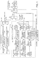
- Fig.1 is a block diagram for detecting the input power source fluctuation in the case of the embodiment 1.
- an input power source fluctuation detection means (2) a converter (CNV) failure detection means, (3) a power supply fluctuation recovery detection means, and (4) a necessary condition of functional operation, will be described using this block diagram.
- CNV converter
- a power supply fluctuation recovery detection means (4) a necessary condition of functional operation
- the input power source fluctuation detector 10 as an input power source fluctuation detection means is equipped with a means to detect change of an input power source directly, and a means to detect the input power source fluctuation by converter controlled variables (CNV controlled variables).
- CNV controlled variables converter controlled variables
- the means (the 1st means) to detect variation of an input power source directly is composed of a voltage fluctuation detector 11a which detect a variation of input power source voltage (VAC), an absolute value detector 11b, and an input voltage level judgment part 11c, etc..
- the voltage fluctuation detector 11a detects a variation of input power source voltage using the derivative element of input voltage, and outputs the detected voltage variation to the absolute value detector 11b.
- a detection procedure and an absolute value detecting method of the above-mentioned voltage variation are well-known technologies, so it has omitted the detailed explanation here.
- the absolute value detector 11b computes the absolute value of the voltage variation inputted from the voltage fluctuation detector 11a, and outputs the computed absolute value to the input voltage level judgment part 11c.
- the input voltage level judgment part 11c compares the absolute value of an input voltage variation inputted from the absolute value detector 11b with an input voltage variation detection level. When the absolute value of voltage variation exceeds the input voltage variation detection level as a result of this comparison, it is regarded that the fluctuation of input voltage (VAC) is detected, and an abnormal input voltage detection signal 11d (for example, 1 (H level)) is outputted.
- VAC fluctuation of input voltage
- an abnormal input voltage detection signal 11d for example, 1 (H level)
- the abnormal input voltage detection signal 11d outputted from input voltage level judgment part 11c is inputted to an OR circuit 14.
- the OR circuit 14 receives the input of the abnormal input voltage detection signal 11d, regards it as the input power source fluctuation is detected, and outputs an input power source fluctuation detection signal 14a.
- the input power source fluctuation detection signal 14a is inputted to one terminal of AND circuit 31.
- a converter failure detection signal 23a is inputted into the terminal of another side of the AND circuit 31. Therefore, when the input power source fluctuation detection signal 14a is outputted and the CNV failure detection signal 23a mentioned above is also outputted, the logic AND conditions of the input signal are satisfied, the flip-flop 32 is set, and a CNV gate block flag (FLG_CNV_GB) is outputted from the output terminal Q of the flip-flop 32.
- the And circuit 31 has a function as a CNV gate block means which carries out the gate block of the converter during the period when the CNV gate block flag (FLG_CNV_GB) is outputted from the output terminal of the flip-flop 32.
- a DC under-voltage detection signal 30a When the abnormalities in DC voltage (for example, DC under-voltage) mentioned later are detected by a DC voltage level judgment part 30, a DC under-voltage detection signal 30a will be outputted from the DC voltage level judgment part 30, and it will be inputted into another terminal of the AND circuit 33.
- DC under-voltage detection signal 30a When the abnormalities in DC voltage (for example, DC under-voltage) mentioned later are detected by a DC voltage level judgment part 30, a DC under-voltage detection signal 30a will be outputted from the DC voltage level judgment part 30, and it will be inputted into another terminal of the AND circuit 33.
- the converter converts an AC power supply as an input power source to a DC power supply. Therefore, the input power source fluctuation is detectable by detecting the variation of input power source directly as having mentioned above. On the other hand, there is a means to detect by the converter controlled variable which controls the converter, when the input power source fluctuation occurred.
- a means (the 2nd means) to detect a variation of converter control current is composed of a current fluctuation detector 12a, an absolute value detector 12b, a converter control current level judgment part (CNV control current level judgment part) 12c, etc.
- converter control current there is converter d-axis current feedback (CNV d-axis current FBK), for example.
- the current fluctuation detector 12a compares the CNV d-axis current FBK with a converter d-axis current reference (not shown).
- the current fluctuation detector 12a detects the current variation, and outputs it to the absolute value detector 12b.
- the absolute value detector 12b computes the absolute value of the current variation inputted from the current fluctuation detector 12a, and outputs it to the CNV control current level judgment part 12c.
- the CNV control current level judgment part 12c compares the absolute value of the current variation inputted from the absolute value detector 12b with a CNV control current detection level (not shown). When the absolute value of current variation exceeds a CNV control current detection level as a result of this comparison, it is regarded as that a CNV control current fluctuation is detected, and an abnormal CNV control current detection signal 12d (for example, 1 (H level)) is outputted to an OR circuit 14.
- a CNV control current detection signal 12d for example, 1 (H level)
- the OR circuit 14 When the OR circuit 14 receives the abnormal CNV control current detection signal 12d, the OR circuit 14 regards it as the input power source fluctuation is detected, and outputs the input power source fluctuation detection signal 14a.
- the input power source fluctuation detection signal 14a is inputted into one terminal of an AND circuit 31. Abnormalities of PLL are also detectable by detecting the CNV control current mentioned above.
- a means (the 3rd means) to detect the variation of converter control voltage is composed of an absolute value detector 13a, a converter control voltage level judgment part 13b, etc.
- converter control voltage CNV control voltage
- converter d-axis voltage feedback CNV d-axis voltage FBK
- Absolute value detector 13a computes inputted absolute value of the CNV d-axis voltage FBK, and outputs it to the CNV control voltage level judgment part 13b.
- the CNV control voltage level judgment part 13b compares the absolute value of the CNV d-axis voltage FBK inputted from an absolute value calculation part 13a, with a CNV control voltage detection level (not shown). When the absolute value of the CNV control voltage exceeds The CNV control voltage detection level as a result of this comparison, it is regarded as that a CNV control voltage fluctuation is detected, and an abnormal CNV control voltage detection signal 13c (for example, 1 (H level)) is outputted.
- the abnormal CNV control voltage detection signal 13c outputted from the CNV control voltage level judgment part 13b is inputted into the OR circuit 14.
- the operation after the input power source fluctuation is detected by the input power source fluctuation detector 10 is as having mentioned above.
- a converter failure detection part 20 has a converter current level judgment part (CNV current level judgment part) 21 and a converter DC voltage level judgment part (CNV DC voltage level judgment part) 22.
- the CNV current level judgment part 21 compares a CNV current (I_CNV) with a converter current reference (a CNV current reference, not shown). When the CNV current exceeds a CNV current reference as a result of this comparison, it is regarded that the overcurrent is detected, and an overcurrent detection signal 21a is outputted.
- the overcurrent detection signal 21a is inputted into an OR circuit 23.
- the OR circuit 23 regards it as the overcurrent in a converter are detected, and outputs the CNV failure detection signal 23a.
- the CNV DC voltage level judgment part 22 compares the CNV DC voltage (VDC) with a converter DC voltage reference (a CNV DC voltage reference, not shown). When the CNV DC voltage exceeds the CNV DC voltage reference as a result of this comparison, it is regarded that an overvoltage is detected, and an overvoltage detection signal 22a is outputted.
- the overvoltage detection signal 22a is inputted into the OR circuit 23.
- the OR circuit 23 regards it as the overvoltage in a converter are detected, and outputs the CNV failure detection signal 23a.
- a CNV control voltage recovery level judgment part 15 compares the absolute value of the CNV d-axis voltage FBK outputted from the absolute value calculation part 13a, with a CNV control voltage recovery level (not shown). When the CNV d-axis voltage FBK is below the CNV control voltage recovery level as a result of this comparison, the flip-flop circuit 32 is reset since it is regarded that the power supply is normal or the power supply fluctuation is returned normally.
- Necessary condition for setting the CNV gate block flag (FLG_CNV_GB) and the inverter control changeover flag (FLG_INV) is a case where a CNV current (I_CNV) turns into overcurrent, or a case where a CNV DC voltage (VDC) turns into overvoltage.
- the gate block (stop) of the converter is not carried out only by detecting the fluctuation of an input power source, but it becomes over-current or overvoltage only when the gate block is carried out during the power supply fluctuation is detected. Since malfunction by incorrect detection is prevented and the possibility of continued operation as a power supply system is made to improve by this, the condition concerned is called the necessary condition of functional operation.
- the flip-flop circuit 32 is set under predetermined requirements when AND conditions are satisfied by above-mentioned AND circuit 31, and the power supply fluctuation by which the functional operation necessary condition mentioned above is fulfilled is detected, and the power supply fluctuation detection signal 31a is outputted from the AND circuit 31.
- predetermined requirements are that it is regarded as the power supply fluctuation is continuing, and a terminal R of the flip-flop 32 is released, when the absolute value of the CNV d-axis voltage FBK is not detected by the CNV control voltage recovery level judgment part 15.
- the gate block of the converter is carried out and the abnormalities of overcurrent and overvoltage are avoided. Moreover, the converter continues operation by diode rectification and the inverter continues its operation similarly.
- Fig. 2 is a block diagram explaining the inverter control using the inverter control change flag (FLG_INV) outputted at the time of the input power source fluctuation concerning with Fig. 1 , and it will be explained also referring to Fig. 1 .
- a rotating speed of a motor 52 is detected by a speed detector 47, and is inputted into a speed controller 42.
- the speed controller 42 controls the rotating speed of the motor 52 in the permitted range set up in a speed reference setting part 41, by comparing the rotating speed detected by the speed detecting part 47 with a speed set up in the speed reference setting part 41.
- the INV control change flag (FLG_INV) outputted from the AND circuit 33 is inputted into a torque and the field reference setting part 43 during a period of that the motor 52 is controlled by the speed controller 42 so that the rotating speed is controlled to meet with the setting speed reference by the speed reference setting part 41.
- the torque and the field reference setting part 43 operate a torque reference and a field reference to carry out a continuous operation of the motor 52 as long as possible.
- a torque reference setting part 43a sets up a torque reference for driving the motor 52.
- the torque reference is reduced to keep or increase DC voltage (VDC) (refer to Fig. 3 (4) and (F)).
- a field reference setting part 43b sets up a field reference for driving the motor 52. For example, in the field weakening control, when a modulation factor has reached saturation ( Fig. 3 (3), (D)), weakens a field flux to reduces the modulation factor and releasing saturation, then restores the field flux gradually (refer to Fig. 3 (3), (D), (E)).
- the modulation factor may increase and it may reach saturation.
- the field reference setting part 43b performs a setup which weakens the field flux of the motor 52 with the fall of DC voltage. Thereby (field weakening control, Fig. 3 (3)), above-mentioned modulation factor is made to increase gently ( Fig. 3 (3), (D)), and makes it possible to hold the rotating speed, field flux, and torque of a motor in the tolerance range for a longer time.
- the torque reduction control and the field weakening control which are mentioned above can be performed by combining either or both.
- the purpose of these control permits the fall of the DC voltage (VDC) within tolerance level, keeps the DC voltage within tolerance level, and continues operation of the motor 52 in possible time range.
- the field reference set up in the field reference setting part 43b and the torque reference set up in the torque reference setting part 43a are inputted into a current reference calculating part 44.
- the current reference calculating part 44 performs calculation for continuing operation mentioned above based on the torque reference and the field reference having been inputted, and sets up a current reference, and inputs it into a current controller 45.
- the current controller 45 compares the current of the motor 52 detected by the current detecting part 46 with a current reference set up by the current reference calculating part 44.
- the comparative result is inputted into a voltage reference setting part 48.
- the voltage reference setting part 48 sets up a voltage reference based on the comparative result inputted from the current control part 45, and inputs it into a PWM controller 49.
- the PWM control part 49 sets up pulse width, the number of pulses, etc. based on the voltage reference inputted from the voltage reference setting part 48, and inputs them into CNV/INV51.
- the CNV (converter)/INV (inverter) 51 carry out following operations, based on pulse width, the number of pulses, etc. which were inputted from the PWM controller 49.
- a CNV part of CNV/INV51 generates a DC electric power from an AC electric power outputted from the generator 50
- INV part of CNV/INV51 generates an AC electric power required to drive the motor 52 based on the above-mentioned DC electric power.
- the CNV gate block flag (FLG_CNV_GB) is inputted into the CNV/INV51 from the flip-flop 32.
- the CNV gate block flag when the CNV gate block flag is set, only the converter (CNV) performs gate-block, although inverter performs its control, such as torque reduction control or field weakening control, based on this signal.
- Fig. 3 is a timing chart explaining the inverter control at the time of the input power source fluctuation detection concerning with Fig. 2 .
- each performance which can be carried out at the time of (1) normal power source, (2) (FLG_CNV_GB) ON operation, (3) field weakening operation, (4) torque reduction operation, (5) (CNV_GB) ON operation, and (6) normal power source recovery will be explained.
- 0 the reset state
- direct voltage, motor speed, a modulation factor, field flux, and torque current are performing stationary behavior. Therefore, it is assumed that stationary behavior is performed on the illustrated level.
- a modulation factor increases gently by suppressing the saturation of the modulation factor by weakening field flux ((E), (D)). As a result, even if DC voltage falls, motor speed, field flux, and torque will be held in the suitable range.
- the converter can avoid overcurrent and overvoltage by carrying out the gate block of it, and the inverter can reduce torque current and keep continues operation with proper field flux, in the case where PLL control becomes unusual according to the power supply fluctuation.
- the inverter keeps continuous operation by limiting on the peak DC voltage of diode rectification, and keep motor speed by field weakening.
Landscapes
- Engineering & Computer Science (AREA)
- Power Engineering (AREA)
- Inverter Devices (AREA)
- Control Of Ac Motors In General (AREA)
Abstract
Description
- The embodiment of the present invention relates to the power conversion apparatus in which the continuous operation of an inverter is possible at the time of an input power source fluctuation.
- For example, when an input voltage of a drive equipment such as an inverter changed according to the input power source fluctuation, an output of PWM converter may generally result in overcurrent or overvoltage. This is because PLL control of converter output voltage cannot be followed to the input power source fluctuation.
- In a PWM converter, when PLL control become unusual, the converter output and the inverter output are used to suspend with the gating signal (hereinafter, a gate block is called.) like a case when general momentary power failure occurred. And when the input power source fluctuation is eliminated, the converter and the inverter are restarted. (For example, refer to
Patent documents 1.). - Patent document 1: Japanese Patent Application Publication No.
2009-273281 - However, by a method given in the patent document mentioned above, other equipment is needed in case of a system accident, such as overcurrent consumption equipment. Moreover, the method does not perform suitable control with the inverter.
- The present invention is made in order to solve the subject mentioned above. The present invention makes it an object to provide a power conversion apparatus in the case where PLL control becomes unusual according to the input power source fluctuation etc., avoiding overcurrent and overvoltage of the converter by carrying out the gate block of the converter, operating the inverter continuously by reducing torque current, and keeping DC voltage and field flux, or to provide a power conversion apparatus to keep a motor speed by a field weakening in which DC voltage is limited on the peak of diode rectification.
- In order to achieve the above-mentioned purpose, the power conversion apparatus of the present invention has a converter(CNV) which converts an AC power to a DC power, an inverter(INV) which converts the DC power to an AC power, a fluctuation detecting means to detect an input power source fluctuation, a gate blocking means to gate block the converter when the input power source fluctuation is detected by the fluctuation detecting means, and a necessary condition of functional operation is satisfied, an inverter control changeover means to switch a contents of inverter control when a converter gate blocking flag is outputted from the gate blocking means, and a DC voltage of the DC power is under a threshold voltage, and an inverter control means to control the inverter based on a inverter control changeover flag outputted from inverter control changeover means, wherein when the input power source fluctuation is detected by the fluctuation detecting means, the converter is gate blocked by the converter gate blocking flag, and the inverter control means continuously operate the inverter while the inverter control changeover flag is outputted.
- According to the present invention, an operation of the inverter can be continued, by reducing the torque current of an inverter and keeping DC voltage and field flux, avoiding overcurrent and overvoltage of the converter by carrying out the gate block of the converter power output, at the time of the input power source fluctuation detection.
-
- [
Fig. 1 ] A block diagram for detecting an input power source fluctuation in the case of theembodiment 1. - [
Fig. 2 ] A block diagram explaining the inverter control using the inverter control changeover flag outputted at the time of the input power source fluctuation detection concerning withFig. 1 . - [
Fig. 3 ] A timing chart explaining the inverter control at the time of the input power source fluctuation detection concerning withFig. 2 . - Hereinafter, embodiment of the present invention will be described with reference to the drawings.
-
Fig.1 is a block diagram for detecting the input power source fluctuation in the case of theembodiment 1. Hereinafter, (1) an input power source fluctuation detection means, (2) a converter (CNV) failure detection means, (3) a power supply fluctuation recovery detection means, and (4) a necessary condition of functional operation, will be described using this block diagram. - The input power
source fluctuation detector 10 as an input power source fluctuation detection means is equipped with a means to detect change of an input power source directly, and a means to detect the input power source fluctuation by converter controlled variables (CNV controlled variables). - The means (the 1st means) to detect variation of an input power source directly is composed of a
voltage fluctuation detector 11a which detect a variation of input power source voltage (VAC), anabsolute value detector 11b, and an input voltagelevel judgment part 11c, etc.. - The
voltage fluctuation detector 11a detects a variation of input power source voltage using the derivative element of input voltage, and outputs the detected voltage variation to theabsolute value detector 11b. A detection procedure and an absolute value detecting method of the above-mentioned voltage variation are well-known technologies, so it has omitted the detailed explanation here. - The
absolute value detector 11b computes the absolute value of the voltage variation inputted from thevoltage fluctuation detector 11a, and outputs the computed absolute value to the input voltagelevel judgment part 11c. The input voltagelevel judgment part 11c compares the absolute value of an input voltage variation inputted from theabsolute value detector 11b with an input voltage variation detection level. When the absolute value of voltage variation exceeds the input voltage variation detection level as a result of this comparison, it is regarded that the fluctuation of input voltage (VAC) is detected, and an abnormal inputvoltage detection signal 11d (for example, 1 (H level)) is outputted. The abnormal inputvoltage detection signal 11d outputted from input voltagelevel judgment part 11c is inputted to anOR circuit 14. - The
OR circuit 14 receives the input of the abnormal inputvoltage detection signal 11d, regards it as the input power source fluctuation is detected, and outputs an input power sourcefluctuation detection signal 14a. The input power sourcefluctuation detection signal 14a is inputted to one terminal ofAND circuit 31. - When abnormalities in the converter mentioned later are detected by a
CNV failure detector 20, a converterfailure detection signal 23a is inputted into the terminal of another side of theAND circuit 31. Therefore, when the input power sourcefluctuation detection signal 14a is outputted and the CNVfailure detection signal 23a mentioned above is also outputted, the logic AND conditions of the input signal are satisfied, the flip-flop 32 is set, and a CNV gate block flag (FLG_CNV_GB) is outputted from the output terminal Q of the flip-flop 32. The Andcircuit 31 has a function as a CNV gate block means which carries out the gate block of the converter during the period when the CNV gate block flag (FLG_CNV_GB) is outputted from the output terminal of the flip-flop 32. - When the abnormalities in DC voltage (for example, DC under-voltage) mentioned later are detected by a DC voltage
level judgment part 30, a DC under-voltage detection signal 30a will be outputted from the DC voltagelevel judgment part 30, and it will be inputted into another terminal of theAND circuit 33. - When the flip-
flop 32 is set and the CNV gate block flag (FLG_CNV_GB) is being output as a result of output of above-mentioned input power sourcefluctuation detection signal 14a and the CNVfailure detecting signal 23a, and when the DC under-voltage detection signal 30a is outputted from the DC voltagelevel judgment part 30, and inputted into theAND circuit 33, then an INV control change flag (FLG_INV) is outputted from the output terminal of theAND circuit 33. During the period when the INV control change flag (FLG_INV) is outputted from the output terminal of theAND circuit 33, theAND circuit 33 has a function as an INV control changeover means in order to carry out continuous operation of the inverter, in spite of the gate block of the converter. - The converter converts an AC power supply as an input power source to a DC power supply. Therefore, the input power source fluctuation is detectable by detecting the variation of input power source directly as having mentioned above. On the other hand, there is a means to detect by the converter controlled variable which controls the converter, when the input power source fluctuation occurred.
- There are two detection means using converter controlled variables. One is to detect variation of converter control current which detects the abnormalities of converter control current (the 2nd means), the other is to detect variation of converter control voltage which detects abnormalities of converter control voltage (the 3rd means). A means (the 2nd means) to detect a variation of converter control current is composed of a
current fluctuation detector 12a, anabsolute value detector 12b, a converter control current level judgment part (CNV control current level judgment part) 12c, etc. As converter control current (CNV control current), there is converter d-axis current feedback (CNV d-axis current FBK), for example. - The
current fluctuation detector 12a compares the CNV d-axis current FBK with a converter d-axis current reference (not shown). Thecurrent fluctuation detector 12a detects the current variation, and outputs it to theabsolute value detector 12b. Theabsolute value detector 12b computes the absolute value of the current variation inputted from thecurrent fluctuation detector 12a, and outputs it to the CNV control currentlevel judgment part 12c. - The CNV control current
level judgment part 12c compares the absolute value of the current variation inputted from theabsolute value detector 12b with a CNV control current detection level (not shown). When the absolute value of current variation exceeds a CNV control current detection level as a result of this comparison, it is regarded as that a CNV control current fluctuation is detected, and an abnormal CNV controlcurrent detection signal 12d (for example, 1 (H level)) is outputted to anOR circuit 14. - When the
OR circuit 14 receives the abnormal CNV controlcurrent detection signal 12d, theOR circuit 14 regards it as the input power source fluctuation is detected, and outputs the input power sourcefluctuation detection signal 14a. The input power sourcefluctuation detection signal 14a is inputted into one terminal of anAND circuit 31. Abnormalities of PLL are also detectable by detecting the CNV control current mentioned above. - A means (the 3rd means) to detect the variation of converter control voltage is composed of an
absolute value detector 13a, a converter control voltagelevel judgment part 13b, etc. As converter control voltage (CNV control voltage), there is converter d-axis voltage feedback (CNV d-axis voltage FBK), for example.Absolute value detector 13a computes inputted absolute value of the CNV d-axis voltage FBK, and outputs it to the CNV control voltagelevel judgment part 13b. - The CNV control voltage
level judgment part 13b compares the absolute value of the CNV d-axis voltage FBK inputted from an absolutevalue calculation part 13a, with a CNV control voltage detection level (not shown). When the absolute value of the CNV control voltage exceeds The CNV control voltage detection level as a result of this comparison, it is regarded as that a CNV control voltage fluctuation is detected, and an abnormal CNV controlvoltage detection signal 13c (for example, 1 (H level)) is outputted. The abnormal CNV controlvoltage detection signal 13c outputted from the CNV control voltagelevel judgment part 13b is inputted into theOR circuit 14. - The operation after the input power source fluctuation is detected by the input power
source fluctuation detector 10 is as having mentioned above. - A converter
failure detection part 20 has a converter current level judgment part (CNV current level judgment part) 21 and a converter DC voltage level judgment part (CNV DC voltage level judgment part) 22. The CNV currentlevel judgment part 21 compares a CNV current (I_CNV) with a converter current reference (a CNV current reference, not shown). When the CNV current exceeds a CNV current reference as a result of this comparison, it is regarded that the overcurrent is detected, and anovercurrent detection signal 21a is outputted. Theovercurrent detection signal 21a is inputted into an ORcircuit 23. - When the
overcurrent detection signal 21a is inputted from the CNV currentlevel judgment part 21, theOR circuit 23 regards it as the overcurrent in a converter are detected, and outputs the CNVfailure detection signal 23a. - The CNV DC voltage
level judgment part 22 compares the CNV DC voltage (VDC) with a converter DC voltage reference (a CNV DC voltage reference, not shown). When the CNV DC voltage exceeds the CNV DC voltage reference as a result of this comparison, it is regarded that an overvoltage is detected, and anovervoltage detection signal 22a is outputted. Theovervoltage detection signal 22a is inputted into theOR circuit 23. When theovervoltage detection signal 22a is inputted from the CNV DC voltagelevel judgment part 22, theOR circuit 23 regards it as the overvoltage in a converter are detected, and outputs the CNVfailure detection signal 23a. - It is judged by the CNV control voltage recovery
level judgment part 15 whether the power supply is normal or the power supply fluctuation mentioned above is returned normally. A CNV control voltage recoverylevel judgment part 15 compares the absolute value of the CNV d-axis voltage FBK outputted from the absolutevalue calculation part 13a, with a CNV control voltage recovery level (not shown). When the CNV d-axis voltage FBK is below the CNV control voltage recovery level as a result of this comparison, the flip-flop circuit 32 is reset since it is regarded that the power supply is normal or the power supply fluctuation is returned normally. - Necessary condition for setting the CNV gate block flag (FLG_CNV_GB) and the inverter control changeover flag (FLG_INV) is a case where a CNV current (I_CNV) turns into overcurrent, or a case where a CNV DC voltage (VDC) turns into overvoltage. In configuration of the present application, the gate block (stop) of the converter is not carried out only by detecting the fluctuation of an input power source, but it becomes over-current or overvoltage only when the gate block is carried out during the power supply fluctuation is detected. Since malfunction by incorrect detection is prevented and the possibility of continued operation as a power supply system is made to improve by this, the condition concerned is called the necessary condition of functional operation.
- The flip-
flop circuit 32 is set under predetermined requirements when AND conditions are satisfied by above-mentioned ANDcircuit 31, and the power supply fluctuation by which the functional operation necessary condition mentioned above is fulfilled is detected, and the power supplyfluctuation detection signal 31a is outputted from the ANDcircuit 31. Above-mentioned predetermined requirements are that it is regarded as the power supply fluctuation is continuing, and a terminal R of the flip-flop 32 is released, when the absolute value of the CNV d-axis voltage FBK is not detected by the CNV control voltage recoverylevel judgment part 15. When this requirement is satisfied and the above-mentioned power supplyfluctuation detection signal 31a is outputted, the above-mentioned power supply fluctuation is able to be detected. - By the CNV gate block flag (FLG_CNV_GB) which is an output of the flip-
flop circuit 32, the gate block of the converter is carried out and the abnormalities of overcurrent and overvoltage are avoided. Moreover, the converter continues operation by diode rectification and the inverter continues its operation similarly. -
Fig. 2 is a block diagram explaining the inverter control using the inverter control change flag (FLG_INV) outputted at the time of the input power source fluctuation concerning withFig. 1 , and it will be explained also referring toFig. 1 . A rotating speed of amotor 52 is detected by aspeed detector 47, and is inputted into aspeed controller 42. Thespeed controller 42 controls the rotating speed of themotor 52 in the permitted range set up in a speedreference setting part 41, by comparing the rotating speed detected by thespeed detecting part 47 with a speed set up in the speedreference setting part 41. - When a power failure is detected by the power supply fluctuation explained in
Fig. 1 , the INV control change flag (FLG_INV) outputted from the ANDcircuit 33 is inputted into a torque and the fieldreference setting part 43 during a period of that themotor 52 is controlled by thespeed controller 42 so that the rotating speed is controlled to meet with the setting speed reference by the speedreference setting part 41. When the INV control change flag is inputted and above-mentioned power failure is detected, the torque and the fieldreference setting part 43 operate a torque reference and a field reference to carry out a continuous operation of themotor 52 as long as possible. - A torque
reference setting part 43a sets up a torque reference for driving themotor 52. For example, in the torque reduction control which reduces torque, the torque reference is reduced to keep or increase DC voltage (VDC) (refer toFig. 3 (4) and (F)). - A field
reference setting part 43b sets up a field reference for driving themotor 52. For example, in the field weakening control, when a modulation factor has reached saturation (Fig. 3 (3), (D)), weakens a field flux to reduces the modulation factor and releasing saturation, then restores the field flux gradually (refer toFig. 3 (3), (D), (E)). - For example, when the gate block of the CNV is carried out and DC voltage falls during the period while the INV control change flag (FLG_INV) signal is outputted, the modulation factor may increase and it may reach saturation. In this case of the operation, in order to prevent this, the following is performed. The field
reference setting part 43b performs a setup which weakens the field flux of themotor 52 with the fall of DC voltage. Thereby (field weakening control,Fig. 3 (3)), above-mentioned modulation factor is made to increase gently (Fig. 3 (3), (D)), and makes it possible to hold the rotating speed, field flux, and torque of a motor in the tolerance range for a longer time. - The torque reduction control and the field weakening control which are mentioned above can be performed by combining either or both. The purpose of these control permits the fall of the DC voltage (VDC) within tolerance level, keeps the DC voltage within tolerance level, and continues operation of the
motor 52 in possible time range. - The field reference set up in the field
reference setting part 43b and the torque reference set up in the torquereference setting part 43a are inputted into a currentreference calculating part 44. - The current
reference calculating part 44 performs calculation for continuing operation mentioned above based on the torque reference and the field reference having been inputted, and sets up a current reference, and inputs it into acurrent controller 45. Thecurrent controller 45 compares the current of themotor 52 detected by the current detectingpart 46 with a current reference set up by the currentreference calculating part 44. The comparative result is inputted into a voltagereference setting part 48. The voltagereference setting part 48 sets up a voltage reference based on the comparative result inputted from thecurrent control part 45, and inputs it into aPWM controller 49. - The
PWM control part 49 sets up pulse width, the number of pulses, etc. based on the voltage reference inputted from the voltagereference setting part 48, and inputs them into CNV/INV51. The CNV (converter)/INV (inverter) 51 carry out following operations, based on pulse width, the number of pulses, etc. which were inputted from thePWM controller 49. A CNV part of CNV/INV51 generates a DC electric power from an AC electric power outputted from thegenerator 50, and INV part of CNV/INV51 generates an AC electric power required to drive themotor 52 based on the above-mentioned DC electric power. - The CNV gate block flag (FLG_CNV_GB) is inputted into the CNV/INV51 from the flip-
flop 32. As mentioned above, when the CNV gate block flag is set, only the converter (CNV) performs gate-block, although inverter performs its control, such as torque reduction control or field weakening control, based on this signal. -
Fig. 3 is a timing chart explaining the inverter control at the time of the input power source fluctuation detection concerning withFig. 2 . Hereinafter, each performance which can be carried out at the time of (1) normal power source, (2) (FLG_CNV_GB) ON operation, (3) field weakening operation, (4) torque reduction operation, (5) (CNV_GB) ON operation, and (6) normal power source recovery will be explained. - A power source abnormal bit which is set in the case of power failure at the time of a power supply abnormal performance, is in the reset state ("0" levels). At the time of normal power supply, it is assumed hereafter that direct voltage, motor speed, a modulation factor, field flux, and torque current are performing stationary behavior. Therefore, it is assumed that stationary behavior is performed on the illustrated level.
- It is in the state (FLG_CNV_GB is "1" level) when the flip-
flop 32 is set at the time of (FLG_CNV_GB) ON operation, and it is in the state when the power supply fluctuation is detected. As one of the correspondences in this case, the gate block of the converter is carried out and the method of continuous operation of the inverter is used.Fig. 3 shows operation of this state. - Since the gate block of the converter is carried out at this time, DC voltage falls ((2) (B)). On the other hand, with the fall of DC voltage, the modulation factor increases in inverse proportion ((2) (D) a). When the modulation factor is within a tolerance level, motor speed, field flux, and torque are held in a suitable range ((2) (C), (E) a, (F)).
- However, since the modulation factor become to be saturated with increase of it and since the INV control change flag (FLG_INV) is outputted at the time of (FLG_CNV_GB) ON operation, field weakening control can also carried out using this signal. That is, by weakening field flux, in connection with field flux declining gently like the waveform shown in ((2) (E) b), the modulation factor increases gently and it is possible to suppress a saturation of the modulation factor.
- As mentioned above, a modulation factor increases gently by suppressing the saturation of the modulation factor by weakening field flux ((E), (D)). As a result, even if DC voltage falls, motor speed, field flux, and torque will be held in the suitable range.
- Although speed falls((4), (C)) by reducing torque as torque current turns to regenerative (
figure 3 (4), (F)), DC voltage increases gradually ((4), (B)). - When above-mentioned (4) torque reduction operation is stopped, torque will return, increase of DC voltage will stop, DC voltage will fall gradually ((5) (B)), and motor speed will increase ((5) (C)). With the fall of DC voltage, the modulation factor increases ((5) (D)) as mentioned above.
- When the power source returns normally, the INV control change flag (FLG_INV) which is an output signal of the AND circuit 18 will be come by off. AS a result, DC voltage ((6) (B)), motor speed ((6) (C)), and the modulation factor ((6) (D)) return to normal status.
- As described above, it is possible to provide a power conversion apparatus, in which the converter can avoid overcurrent and overvoltage by carrying out the gate block of it, and the inverter can reduce torque current and keep continues operation with proper field flux, in the case where PLL control becomes unusual according to the power supply fluctuation. Or it is possible to provide a power conversion apparatus in which the inverter keeps continuous operation by limiting on the peak DC voltage of diode rectification, and keep motor speed by field weakening.
-
- 10 INPUT POWER SOURCE FLUCTUATION DETECTOR
- 11a VOLTAGE FLUCTIATION DETECTOR
- 11b ABSOLUTE VALUE DETCTOR
- 11c INPUT VOLTAGE LEVEL JUDGEMENT PART
- 12a VOLTAGE FLUCTUATION DETECTOR
- 12b ABSOLUTE VALUE DETCTOR
- 12c CONVERTER CONTROL CURRENT LEVEL JUDGEMENT PART
- 13a ABSOLUTE VALUE DETCTOR
- 13b CONVERTER CONTROL VOLTAGE LEVEL JUDGEMENT PART
- 14 OR CIRCUIT
- 15 CONVERTER CONTROL VOLTAGE RECOVERY LEVEL JUDGEMENT PART
- 20 CONVERTER FAILURE DETECTOR
- 21 CONVERTER CURRENT LEVEL JUDGEMENT PART
- 22 CONVERTER DC VOLTAGE LEVEL JUDGEMENT PART
- 23 OR CIRCUIT
- 30 DC VOLTAGE LEVEL JUDGEMENT PART
- 31, 33 AND CIRCUIT
- 32 FLIP-FLOP
- 41 SPEED REFFERENCE SETTING PART
- 42 SPEED CONTROLER
- 43 TORQUE/ FIELD REFFERENCE SETTING PART
- 44 CURRENT REFFERENCE CALCULATING PART
- 45 CURRENT CONTROLER
- 46 CURRENT DETECTING PART
- 47 SPEED DETECTING PART
- 48 VOLTAGE REFFERENCE SETTING PART
- 49 PWM CONTROLER
- 50 GENERATOR
- 51 CONVERTER AND INVERTER
- 52 MOTOR
Claims (6)
- A power conversion apparatus comprising a converter for converting an AC power to a DC power and an inverter for converting the DC power to an AC power, comprising:a fluctuation detecting means to detect an input power source fluctuation;a gate blocking means to gate block the converter when the input power source fluctuation is detected by the fluctuation detecting means, and when a necessary condition of functional operation is satisfied;an inverter control changeover means to switch a contents of inverter control when a converter gate blocking flag is outputted from the gate blocking means, and when a DC voltage of the DC power is under a threshold voltage; andan inverter control means to control the inverter based on a inverter control changeover flag outputted from the inverter control changeover means;wherein, when the input power source fluctuation is detected by the fluctuation detecting means, the converter is gate blocked by the converter gate blocking flag, and the inverter control means continuously operate the inverter while the inverter control changeover flag has been outputted.
- A power conversion apparatus according to Claim 1,
wherein the fluctuation detecting means has a first detecting means, comprising:a voltage fluctuation detector to detects a variation of input power source voltage directly;an absolute value detector to computes an absolute value of voltage variation inputted from the voltage fluctuation detector;an input voltage level judgment part which outputs an abnormal input voltage detection signal as it is regarded that the fluctuation of input voltage is detected, when the absolute value of voltage variation exceeds an input voltage variation detection level in comparison of them. - A power conversion apparatus according to Claim 1,
wherein the fluctuation detecting means has a second detecting means, comprising:a current fluctuation detector to detect a variation of converter d-axis current feedback as a converter control current;an absolute value detector to computes the absolute value of current variation inputted from the current fluctuation detector;a converter control current level judgment part which outputs the abnormal converter control current detection signal as it is regarded that the fluctuation of converter control current is detected, when the absolute value of control current variation exceeds a control current variation detection level in comparison of them.and, the fluctuation detecting means has a third detecting means, comprising:an absolute value detector to computes an absolute value of voltage variation of a converter d-axis voltage feedback as a converter control voltage;a converter control voltage level judgment part which outputs an abnormal converter control voltage detection signal as it is regarded that the fluctuation of converter control voltage is detected, when the absolute value of control voltage variation exceeds a control voltage variation detection level in comparison of them. - A power conversion apparatus according to Claim 1,
wherein, the inverter control means is able to keep motor speed, field flux, and torque in the suitable range, when the converter is gate blocked by the converter gate blocking flag, since the modulation factor increases with the fall of DC voltage. - A power conversion apparatus according to Claim 1,
wherein, the inverter control means further comprising a field reference setting part, which performs field weakening setting with the fall of DC voltage in the period of the inverter control changeover flag inputted, to increase the modulation factor gently for keeping motor speed, field flux, and torque as long time as possible in a suitable range, when the converter is gate blocked by the converter gate blocking flag and DC voltage fall. - A power conversion apparatus according to Claim 1,
wherein, the inverter control means further comprising a torque reference setting part, which performs torque reduction setting in the period of the inverter control changeover flag inputted, to keep or increase the DC voltage when the converter is gate blocked by the converter gate blocking flag and when DC voltage falls.
Applications Claiming Priority (2)
| Application Number | Priority Date | Filing Date | Title |
|---|---|---|---|
| JP2015208872A JP6452215B2 (en) | 2015-10-23 | 2015-10-23 | Power converter |
| PCT/JP2016/070906 WO2017068821A1 (en) | 2015-10-23 | 2016-07-14 | Power conversion device |
Publications (3)
| Publication Number | Publication Date |
|---|---|
| EP3367554A1 true EP3367554A1 (en) | 2018-08-29 |
| EP3367554A4 EP3367554A4 (en) | 2019-06-19 |
| EP3367554B1 EP3367554B1 (en) | 2021-09-29 |
Family
ID=58556959
Family Applications (1)
| Application Number | Title | Priority Date | Filing Date |
|---|---|---|---|
| EP16857139.6A Active EP3367554B1 (en) | 2015-10-23 | 2016-07-14 | Power conversion device |
Country Status (5)
| Country | Link |
|---|---|
| US (1) | US10536105B2 (en) |
| EP (1) | EP3367554B1 (en) |
| JP (1) | JP6452215B2 (en) |
| CN (1) | CN108352793B (en) |
| WO (1) | WO2017068821A1 (en) |
Family Cites Families (10)
| Publication number | Priority date | Publication date | Assignee | Title |
|---|---|---|---|---|
| JPS60139186A (en) * | 1983-12-27 | 1985-07-23 | Toshiba Corp | Controller for motor |
| JPH06121548A (en) * | 1992-10-06 | 1994-04-28 | Mitsubishi Electric Corp | Inverter device |
| JP2007049798A (en) * | 2005-08-09 | 2007-02-22 | Toshiba Mitsubishi-Electric Industrial System Corp | Power conversion equipment |
| JP4834691B2 (en) | 2008-05-09 | 2011-12-14 | 株式会社日立製作所 | Wind power generation system |
| US9340111B2 (en) * | 2010-12-01 | 2016-05-17 | Mitsubishi Electric Corporation | Control device for electric vehicle |
| US8902616B2 (en) * | 2011-10-13 | 2014-12-02 | Rockwell Automation Technologies, Inc. | Active front end power converter with diagnostic and failure prevention using peak detector with decay |
| JP5749632B2 (en) * | 2011-11-18 | 2015-07-15 | 京セラ株式会社 | Power conditioner with DC power supply function and control method thereof |
| JP5784470B2 (en) * | 2011-11-28 | 2015-09-24 | 京セラ株式会社 | Power conditioner and control method thereof |
| JP5689497B2 (en) * | 2013-04-22 | 2015-03-25 | ファナック株式会社 | Motor drive device having DC link unit abnormality detection function |
| JP6358834B2 (en) * | 2014-04-08 | 2018-07-18 | 株式会社日立産機システム | Vector control device, inverter incorporating the same, and inverter and motor setting device incorporating the same |
-
2015
- 2015-10-23 JP JP2015208872A patent/JP6452215B2/en active Active
-
2016
- 2016-07-14 WO PCT/JP2016/070906 patent/WO2017068821A1/en not_active Ceased
- 2016-07-14 EP EP16857139.6A patent/EP3367554B1/en active Active
- 2016-07-14 CN CN201680061512.6A patent/CN108352793B/en active Active
-
2018
- 2018-04-23 US US15/959,691 patent/US10536105B2/en active Active
Also Published As
| Publication number | Publication date |
|---|---|
| EP3367554B1 (en) | 2021-09-29 |
| WO2017068821A1 (en) | 2017-04-27 |
| US20180241338A1 (en) | 2018-08-23 |
| JP2017085703A (en) | 2017-05-18 |
| CN108352793A (en) | 2018-07-31 |
| US10536105B2 (en) | 2020-01-14 |
| CN108352793B (en) | 2021-09-28 |
| JP6452215B2 (en) | 2019-01-16 |
| EP3367554A4 (en) | 2019-06-19 |
Similar Documents
| Publication | Publication Date | Title |
|---|---|---|
| US8786239B2 (en) | Motor drive PWM rectifier having modulation scheme selector | |
| TWI243532B (en) | Inverter device and current limiting method therefor | |
| US9287698B2 (en) | Power conversion apparatus | |
| US20090218976A1 (en) | Motor driving apparatus | |
| JP5681785B2 (en) | Power converter | |
| US9975433B2 (en) | Electric vehicle controller | |
| EP2955833A1 (en) | Method for voltage dip compensation of inverter | |
| JP5608809B2 (en) | Power converter | |
| JP5134691B2 (en) | Self-excited reactive power compensator | |
| US11128252B2 (en) | Motor drive device | |
| JP5527638B2 (en) | Power regeneration converter, motor drive system | |
| US11496085B2 (en) | Motor drive apparatus | |
| US10389292B1 (en) | DC bus regulation using rectifier and inverter | |
| US10014764B1 (en) | Method for controlling inverter | |
| EP3367554B1 (en) | Power conversion device | |
| JP6258806B2 (en) | Power converter for grid connection | |
| US9751408B2 (en) | Motor driving unit | |
| CN106357132A (en) | Control method and equipment of three-phase three-wire rectifying circuit | |
| JP2002272181A (en) | Power converter | |
| EP3340452B1 (en) | Power conversion device | |
| JP5099873B2 (en) | Inverter current limit control | |
| CN119448157A (en) | A short-circuit protection method and system for AC/DC hybrid microgrid | |
| EP4318905A1 (en) | Direct current junction box, photovoltaic power generation system, and fault detection method | |
| PH12018000166A1 (en) | Motor control apparatus | |
| JPH10174446A (en) | Inverter device |
Legal Events
| Date | Code | Title | Description |
|---|---|---|---|
| STAA | Information on the status of an ep patent application or granted ep patent |
Free format text: STATUS: THE INTERNATIONAL PUBLICATION HAS BEEN MADE |
|
| PUAI | Public reference made under article 153(3) epc to a published international application that has entered the european phase |
Free format text: ORIGINAL CODE: 0009012 |
|
| STAA | Information on the status of an ep patent application or granted ep patent |
Free format text: STATUS: REQUEST FOR EXAMINATION WAS MADE |
|
| 17P | Request for examination filed |
Effective date: 20180419 |
|
| AK | Designated contracting states |
Kind code of ref document: A1 Designated state(s): AL AT BE BG CH CY CZ DE DK EE ES FI FR GB GR HR HU IE IS IT LI LT LU LV MC MK MT NL NO PL PT RO RS SE SI SK SM TR |
|
| AX | Request for extension of the european patent |
Extension state: BA ME |
|
| DAV | Request for validation of the european patent (deleted) | ||
| DAX | Request for extension of the european patent (deleted) | ||
| A4 | Supplementary search report drawn up and despatched |
Effective date: 20190522 |
|
| RIC1 | Information provided on ipc code assigned before grant |
Ipc: H02P 29/024 20160101ALI20190516BHEP Ipc: H02M 1/32 20070101ALI20190516BHEP Ipc: H02P 3/18 20060101AFI20190516BHEP Ipc: H02P 27/06 20060101ALI20190516BHEP Ipc: H02P 27/08 20060101ALI20190516BHEP Ipc: H02H 7/127 20060101ALI20190516BHEP Ipc: H02P 29/032 20160101ALI20190516BHEP |
|
| GRAP | Despatch of communication of intention to grant a patent |
Free format text: ORIGINAL CODE: EPIDOSNIGR1 |
|
| STAA | Information on the status of an ep patent application or granted ep patent |
Free format text: STATUS: GRANT OF PATENT IS INTENDED |
|
| RIC1 | Information provided on ipc code assigned before grant |
Ipc: H02M 1/32 20070101ALI20210413BHEP Ipc: H02P 29/032 20160101ALI20210413BHEP Ipc: H02P 29/024 20160101ALI20210413BHEP Ipc: H02P 27/08 20060101ALI20210413BHEP Ipc: H02H 7/127 20060101ALI20210413BHEP Ipc: H02P 27/06 20060101ALI20210413BHEP Ipc: H02P 3/18 20060101AFI20210413BHEP |
|
| INTG | Intention to grant announced |
Effective date: 20210429 |
|
| GRAS | Grant fee paid |
Free format text: ORIGINAL CODE: EPIDOSNIGR3 |
|
| GRAA | (expected) grant |
Free format text: ORIGINAL CODE: 0009210 |
|
| STAA | Information on the status of an ep patent application or granted ep patent |
Free format text: STATUS: THE PATENT HAS BEEN GRANTED |
|
| AK | Designated contracting states |
Kind code of ref document: B1 Designated state(s): AL AT BE BG CH CY CZ DE DK EE ES FI FR GB GR HR HU IE IS IT LI LT LU LV MC MK MT NL NO PL PT RO RS SE SI SK SM TR |
|
| REG | Reference to a national code |
Ref country code: GB Ref legal event code: FG4D |
|
| REG | Reference to a national code |
Ref country code: CH Ref legal event code: EP Ref country code: AT Ref legal event code: REF Ref document number: 1435099 Country of ref document: AT Kind code of ref document: T Effective date: 20211015 |
|
| REG | Reference to a national code |
Ref country code: DE Ref legal event code: R096 Ref document number: 602016064453 Country of ref document: DE |
|
| REG | Reference to a national code |
Ref country code: IE Ref legal event code: FG4D |
|
| REG | Reference to a national code |
Ref country code: LT Ref legal event code: MG9D |
|
| PG25 | Lapsed in a contracting state [announced via postgrant information from national office to epo] |
Ref country code: RS Free format text: LAPSE BECAUSE OF FAILURE TO SUBMIT A TRANSLATION OF THE DESCRIPTION OR TO PAY THE FEE WITHIN THE PRESCRIBED TIME-LIMIT Effective date: 20210929 Ref country code: SE Free format text: LAPSE BECAUSE OF FAILURE TO SUBMIT A TRANSLATION OF THE DESCRIPTION OR TO PAY THE FEE WITHIN THE PRESCRIBED TIME-LIMIT Effective date: 20210929 Ref country code: NO Free format text: LAPSE BECAUSE OF FAILURE TO SUBMIT A TRANSLATION OF THE DESCRIPTION OR TO PAY THE FEE WITHIN THE PRESCRIBED TIME-LIMIT Effective date: 20211229 Ref country code: HR Free format text: LAPSE BECAUSE OF FAILURE TO SUBMIT A TRANSLATION OF THE DESCRIPTION OR TO PAY THE FEE WITHIN THE PRESCRIBED TIME-LIMIT Effective date: 20210929 Ref country code: FI Free format text: LAPSE BECAUSE OF FAILURE TO SUBMIT A TRANSLATION OF THE DESCRIPTION OR TO PAY THE FEE WITHIN THE PRESCRIBED TIME-LIMIT Effective date: 20210929 Ref country code: LT Free format text: LAPSE BECAUSE OF FAILURE TO SUBMIT A TRANSLATION OF THE DESCRIPTION OR TO PAY THE FEE WITHIN THE PRESCRIBED TIME-LIMIT Effective date: 20210929 Ref country code: BG Free format text: LAPSE BECAUSE OF FAILURE TO SUBMIT A TRANSLATION OF THE DESCRIPTION OR TO PAY THE FEE WITHIN THE PRESCRIBED TIME-LIMIT Effective date: 20211229 |
|
| REG | Reference to a national code |
Ref country code: NL Ref legal event code: MP Effective date: 20210929 |
|
| REG | Reference to a national code |
Ref country code: AT Ref legal event code: MK05 Ref document number: 1435099 Country of ref document: AT Kind code of ref document: T Effective date: 20210929 |
|
| PG25 | Lapsed in a contracting state [announced via postgrant information from national office to epo] |
Ref country code: LV Free format text: LAPSE BECAUSE OF FAILURE TO SUBMIT A TRANSLATION OF THE DESCRIPTION OR TO PAY THE FEE WITHIN THE PRESCRIBED TIME-LIMIT Effective date: 20210929 Ref country code: GR Free format text: LAPSE BECAUSE OF FAILURE TO SUBMIT A TRANSLATION OF THE DESCRIPTION OR TO PAY THE FEE WITHIN THE PRESCRIBED TIME-LIMIT Effective date: 20211230 |
|
| PG25 | Lapsed in a contracting state [announced via postgrant information from national office to epo] |
Ref country code: AT Free format text: LAPSE BECAUSE OF FAILURE TO SUBMIT A TRANSLATION OF THE DESCRIPTION OR TO PAY THE FEE WITHIN THE PRESCRIBED TIME-LIMIT Effective date: 20210929 |
|
| PG25 | Lapsed in a contracting state [announced via postgrant information from national office to epo] |
Ref country code: IS Free format text: LAPSE BECAUSE OF FAILURE TO SUBMIT A TRANSLATION OF THE DESCRIPTION OR TO PAY THE FEE WITHIN THE PRESCRIBED TIME-LIMIT Effective date: 20220129 Ref country code: SK Free format text: LAPSE BECAUSE OF FAILURE TO SUBMIT A TRANSLATION OF THE DESCRIPTION OR TO PAY THE FEE WITHIN THE PRESCRIBED TIME-LIMIT Effective date: 20210929 Ref country code: RO Free format text: LAPSE BECAUSE OF FAILURE TO SUBMIT A TRANSLATION OF THE DESCRIPTION OR TO PAY THE FEE WITHIN THE PRESCRIBED TIME-LIMIT Effective date: 20210929 Ref country code: PT Free format text: LAPSE BECAUSE OF FAILURE TO SUBMIT A TRANSLATION OF THE DESCRIPTION OR TO PAY THE FEE WITHIN THE PRESCRIBED TIME-LIMIT Effective date: 20220131 Ref country code: PL Free format text: LAPSE BECAUSE OF FAILURE TO SUBMIT A TRANSLATION OF THE DESCRIPTION OR TO PAY THE FEE WITHIN THE PRESCRIBED TIME-LIMIT Effective date: 20210929 Ref country code: NL Free format text: LAPSE BECAUSE OF FAILURE TO SUBMIT A TRANSLATION OF THE DESCRIPTION OR TO PAY THE FEE WITHIN THE PRESCRIBED TIME-LIMIT Effective date: 20210929 Ref country code: ES Free format text: LAPSE BECAUSE OF FAILURE TO SUBMIT A TRANSLATION OF THE DESCRIPTION OR TO PAY THE FEE WITHIN THE PRESCRIBED TIME-LIMIT Effective date: 20210929 Ref country code: EE Free format text: LAPSE BECAUSE OF FAILURE TO SUBMIT A TRANSLATION OF THE DESCRIPTION OR TO PAY THE FEE WITHIN THE PRESCRIBED TIME-LIMIT Effective date: 20210929 Ref country code: CZ Free format text: LAPSE BECAUSE OF FAILURE TO SUBMIT A TRANSLATION OF THE DESCRIPTION OR TO PAY THE FEE WITHIN THE PRESCRIBED TIME-LIMIT Effective date: 20210929 Ref country code: AL Free format text: LAPSE BECAUSE OF FAILURE TO SUBMIT A TRANSLATION OF THE DESCRIPTION OR TO PAY THE FEE WITHIN THE PRESCRIBED TIME-LIMIT Effective date: 20210929 |
|
| REG | Reference to a national code |
Ref country code: DE Ref legal event code: R097 Ref document number: 602016064453 Country of ref document: DE |
|
| PG25 | Lapsed in a contracting state [announced via postgrant information from national office to epo] |
Ref country code: DK Free format text: LAPSE BECAUSE OF FAILURE TO SUBMIT A TRANSLATION OF THE DESCRIPTION OR TO PAY THE FEE WITHIN THE PRESCRIBED TIME-LIMIT Effective date: 20210929 |
|
| PLBE | No opposition filed within time limit |
Free format text: ORIGINAL CODE: 0009261 |
|
| STAA | Information on the status of an ep patent application or granted ep patent |
Free format text: STATUS: NO OPPOSITION FILED WITHIN TIME LIMIT |
|
| 26N | No opposition filed |
Effective date: 20220630 |
|
| PG25 | Lapsed in a contracting state [announced via postgrant information from national office to epo] |
Ref country code: SI Free format text: LAPSE BECAUSE OF FAILURE TO SUBMIT A TRANSLATION OF THE DESCRIPTION OR TO PAY THE FEE WITHIN THE PRESCRIBED TIME-LIMIT Effective date: 20210929 |
|
| PG25 | Lapsed in a contracting state [announced via postgrant information from national office to epo] |
Ref country code: IT Free format text: LAPSE BECAUSE OF FAILURE TO SUBMIT A TRANSLATION OF THE DESCRIPTION OR TO PAY THE FEE WITHIN THE PRESCRIBED TIME-LIMIT Effective date: 20210929 |
|
| PG25 | Lapsed in a contracting state [announced via postgrant information from national office to epo] |
Ref country code: MC Free format text: LAPSE BECAUSE OF FAILURE TO SUBMIT A TRANSLATION OF THE DESCRIPTION OR TO PAY THE FEE WITHIN THE PRESCRIBED TIME-LIMIT Effective date: 20210929 |
|
| GBPC | Gb: european patent ceased through non-payment of renewal fee |
Effective date: 20220714 |
|
| REG | Reference to a national code |
Ref country code: BE Ref legal event code: MM Effective date: 20220731 |
|
| PG25 | Lapsed in a contracting state [announced via postgrant information from national office to epo] |
Ref country code: LU Free format text: LAPSE BECAUSE OF NON-PAYMENT OF DUE FEES Effective date: 20220714 Ref country code: FR Free format text: LAPSE BECAUSE OF NON-PAYMENT OF DUE FEES Effective date: 20220731 |
|
| PG25 | Lapsed in a contracting state [announced via postgrant information from national office to epo] |
Ref country code: GB Free format text: LAPSE BECAUSE OF NON-PAYMENT OF DUE FEES Effective date: 20220714 Ref country code: BE Free format text: LAPSE BECAUSE OF NON-PAYMENT OF DUE FEES Effective date: 20220731 |
|
| PG25 | Lapsed in a contracting state [announced via postgrant information from national office to epo] |
Ref country code: IE Free format text: LAPSE BECAUSE OF NON-PAYMENT OF DUE FEES Effective date: 20220714 |
|
| PG25 | Lapsed in a contracting state [announced via postgrant information from national office to epo] |
Ref country code: HU Free format text: LAPSE BECAUSE OF FAILURE TO SUBMIT A TRANSLATION OF THE DESCRIPTION OR TO PAY THE FEE WITHIN THE PRESCRIBED TIME-LIMIT; INVALID AB INITIO Effective date: 20160714 |
|
| PG25 | Lapsed in a contracting state [announced via postgrant information from national office to epo] |
Ref country code: SM Free format text: LAPSE BECAUSE OF FAILURE TO SUBMIT A TRANSLATION OF THE DESCRIPTION OR TO PAY THE FEE WITHIN THE PRESCRIBED TIME-LIMIT Effective date: 20210929 Ref country code: MK Free format text: LAPSE BECAUSE OF FAILURE TO SUBMIT A TRANSLATION OF THE DESCRIPTION OR TO PAY THE FEE WITHIN THE PRESCRIBED TIME-LIMIT Effective date: 20210929 Ref country code: CY Free format text: LAPSE BECAUSE OF FAILURE TO SUBMIT A TRANSLATION OF THE DESCRIPTION OR TO PAY THE FEE WITHIN THE PRESCRIBED TIME-LIMIT Effective date: 20210929 |
|
| PG25 | Lapsed in a contracting state [announced via postgrant information from national office to epo] |
Ref country code: TR Free format text: LAPSE BECAUSE OF FAILURE TO SUBMIT A TRANSLATION OF THE DESCRIPTION OR TO PAY THE FEE WITHIN THE PRESCRIBED TIME-LIMIT Effective date: 20210929 |
|
| PG25 | Lapsed in a contracting state [announced via postgrant information from national office to epo] |
Ref country code: MT Free format text: LAPSE BECAUSE OF FAILURE TO SUBMIT A TRANSLATION OF THE DESCRIPTION OR TO PAY THE FEE WITHIN THE PRESCRIBED TIME-LIMIT Effective date: 20210929 |
|
| PGFP | Annual fee paid to national office [announced via postgrant information from national office to epo] |
Ref country code: DE Payment date: 20250528 Year of fee payment: 10 |
|
| PGFP | Annual fee paid to national office [announced via postgrant information from national office to epo] |
Ref country code: CH Payment date: 20250801 Year of fee payment: 10 |