EP3366808B1 - Method of forming layers on a substrate - Google Patents
Method of forming layers on a substrate Download PDFInfo
- Publication number
- EP3366808B1 EP3366808B1 EP18158881.5A EP18158881A EP3366808B1 EP 3366808 B1 EP3366808 B1 EP 3366808B1 EP 18158881 A EP18158881 A EP 18158881A EP 3366808 B1 EP3366808 B1 EP 3366808B1
- Authority
- EP
- European Patent Office
- Prior art keywords
- substrate
- compound
- dad
- tbu2
- provides
- Prior art date
- Legal status (The legal status is an assumption and is not a legal conclusion. Google has not performed a legal analysis and makes no representation as to the accuracy of the status listed.)
- Active
Links
Images


Classifications
-
- C—CHEMISTRY; METALLURGY
- C23—COATING METALLIC MATERIAL; COATING MATERIAL WITH METALLIC MATERIAL; CHEMICAL SURFACE TREATMENT; DIFFUSION TREATMENT OF METALLIC MATERIAL; COATING BY VACUUM EVAPORATION, BY SPUTTERING, BY ION IMPLANTATION OR BY CHEMICAL VAPOUR DEPOSITION, IN GENERAL; INHIBITING CORROSION OF METALLIC MATERIAL OR INCRUSTATION IN GENERAL
- C23C—COATING METALLIC MATERIAL; COATING MATERIAL WITH METALLIC MATERIAL; SURFACE TREATMENT OF METALLIC MATERIAL BY DIFFUSION INTO THE SURFACE, BY CHEMICAL CONVERSION OR SUBSTITUTION; COATING BY VACUUM EVAPORATION, BY SPUTTERING, BY ION IMPLANTATION OR BY CHEMICAL VAPOUR DEPOSITION, IN GENERAL
- C23C16/00—Chemical coating by decomposition of gaseous compounds, without leaving reaction products of surface material in the coating, i.e. chemical vapour deposition [CVD] processes
- C23C16/06—Chemical coating by decomposition of gaseous compounds, without leaving reaction products of surface material in the coating, i.e. chemical vapour deposition [CVD] processes characterised by the deposition of metallic material
- C23C16/18—Chemical coating by decomposition of gaseous compounds, without leaving reaction products of surface material in the coating, i.e. chemical vapour deposition [CVD] processes characterised by the deposition of metallic material from metallo-organic compounds
-
- C—CHEMISTRY; METALLURGY
- C07—ORGANIC CHEMISTRY
- C07F—ACYCLIC, CARBOCYCLIC OR HETEROCYCLIC COMPOUNDS CONTAINING ELEMENTS OTHER THAN CARBON, HYDROGEN, HALOGEN, OXYGEN, NITROGEN, SULFUR, SELENIUM OR TELLURIUM
- C07F7/00—Compounds containing elements of Groups 4 or 14 of the Periodic Table
- C07F7/02—Silicon compounds
- C07F7/08—Compounds having one or more C—Si linkages
-
- C—CHEMISTRY; METALLURGY
- C23—COATING METALLIC MATERIAL; COATING MATERIAL WITH METALLIC MATERIAL; CHEMICAL SURFACE TREATMENT; DIFFUSION TREATMENT OF METALLIC MATERIAL; COATING BY VACUUM EVAPORATION, BY SPUTTERING, BY ION IMPLANTATION OR BY CHEMICAL VAPOUR DEPOSITION, IN GENERAL; INHIBITING CORROSION OF METALLIC MATERIAL OR INCRUSTATION IN GENERAL
- C23C—COATING METALLIC MATERIAL; COATING MATERIAL WITH METALLIC MATERIAL; SURFACE TREATMENT OF METALLIC MATERIAL BY DIFFUSION INTO THE SURFACE, BY CHEMICAL CONVERSION OR SUBSTITUTION; COATING BY VACUUM EVAPORATION, BY SPUTTERING, BY ION IMPLANTATION OR BY CHEMICAL VAPOUR DEPOSITION, IN GENERAL
- C23C16/00—Chemical coating by decomposition of gaseous compounds, without leaving reaction products of surface material in the coating, i.e. chemical vapour deposition [CVD] processes
- C23C16/44—Chemical coating by decomposition of gaseous compounds, without leaving reaction products of surface material in the coating, i.e. chemical vapour deposition [CVD] processes characterised by the method of coating
- C23C16/455—Chemical coating by decomposition of gaseous compounds, without leaving reaction products of surface material in the coating, i.e. chemical vapour deposition [CVD] processes characterised by the method of coating characterised by the method used for introducing gases into reaction chamber or for modifying gas flows in reaction chamber
- C23C16/45523—Pulsed gas flow or change of composition over time
- C23C16/45525—Atomic layer deposition [ALD]
- C23C16/45527—Atomic layer deposition [ALD] characterized by the ALD cycle, e.g. different flows or temperatures during half-reactions, unusual pulsing sequence, use of precursor mixtures or auxiliary reactants or activations
- C23C16/45534—Use of auxiliary reactants other than used for contributing to the composition of the main film, e.g. catalysts, activators or scavengers
-
- C—CHEMISTRY; METALLURGY
- C23—COATING METALLIC MATERIAL; COATING MATERIAL WITH METALLIC MATERIAL; CHEMICAL SURFACE TREATMENT; DIFFUSION TREATMENT OF METALLIC MATERIAL; COATING BY VACUUM EVAPORATION, BY SPUTTERING, BY ION IMPLANTATION OR BY CHEMICAL VAPOUR DEPOSITION, IN GENERAL; INHIBITING CORROSION OF METALLIC MATERIAL OR INCRUSTATION IN GENERAL
- C23C—COATING METALLIC MATERIAL; COATING MATERIAL WITH METALLIC MATERIAL; SURFACE TREATMENT OF METALLIC MATERIAL BY DIFFUSION INTO THE SURFACE, BY CHEMICAL CONVERSION OR SUBSTITUTION; COATING BY VACUUM EVAPORATION, BY SPUTTERING, BY ION IMPLANTATION OR BY CHEMICAL VAPOUR DEPOSITION, IN GENERAL
- C23C16/00—Chemical coating by decomposition of gaseous compounds, without leaving reaction products of surface material in the coating, i.e. chemical vapour deposition [CVD] processes
- C23C16/44—Chemical coating by decomposition of gaseous compounds, without leaving reaction products of surface material in the coating, i.e. chemical vapour deposition [CVD] processes characterised by the method of coating
- C23C16/455—Chemical coating by decomposition of gaseous compounds, without leaving reaction products of surface material in the coating, i.e. chemical vapour deposition [CVD] processes characterised by the method of coating characterised by the method used for introducing gases into reaction chamber or for modifying gas flows in reaction chamber
- C23C16/45523—Pulsed gas flow or change of composition over time
- C23C16/45525—Atomic layer deposition [ALD]
- C23C16/45553—Atomic layer deposition [ALD] characterized by the use of precursors specially adapted for ALD
Definitions
- the present invention is related to the formation of metal films from "metalorganic" precursors and a reducing agent.
- Atomic layer deposition is a thin film deposition technique that addresses many of the current technological demands.
- ALD affords inherently conformal coverage and sub-nanometer film thickness control due to its self-limited growth mechanism.
- a substrate is contacted with a first chemical composition that modifies the substrate for a first predetermined period of time (a pulse).
- a pulse Such modification involves adsorption to the surface of the substrate, reaction with the surface of the substrate, or a combination of adsorption and reaction.
- a purging gas is introduced to remove any lingering first gaseous chemical composition in the vicinity of the substrate.
- a second gaseous chemical composition that reacts with the modified substrate surface is introduced for a second predetermined period of time into the vicinity of the substrate to form a portion of the thin film.
- a purging gas is subsequently introduced to remove any lingering second chemical composition in the vicinity of the substrate.
- the process comprises contacting a substrate surface with the above-mentioned metal containing compound to form a first modified surface and contacting said modified surface with an activating compound.
- the activating compound may be a reducing agent.
- the present invention as claimed solves one or more problems of the prior art by providing a method of forming a layer on a substrate, the method comprising a deposition cycle including:
- the atom is in a positive oxidation state of 1, 2, 3, 4, 5, or 6.
- the first compound can be selected from bis(dimethylamino-2-propoxy) copper (II) (Cu(dmap)2), bis(dimethylamino-2-propoxy) nickel (II) (Ni(dmap)2, bis(1,4-di-tert-butyldiazene) chromium(II) (Cr(dadtBu2)2), bis(1,4-di-tert-butyldiazene) manganese (II) (Mn(dadtBu2)2), bis(1,4-di-tert-butyldiazene) iron(II) (Fe(dadtBu2)2), bis(1,4-di-tert-butyldiazene) cobalt(II) (Co(dadtBu2)2) and bis(1,4-di-tert-butyldiazene) nickel(II) (Ni(dadtBu2)2).
- the substrate is additionally contacted with the vapor of the first compound having an atom in an oxidized state, the acid, and the vapor of a reducing agent during a plurality of additional deposition cycles.
- the substrate can be selected from SiH and Co when said first compound is Cu(dmap)2, Si when said first compound is Ni(Dmap)2, Ru when said first compound is Ni(Dmap)2 or Ni(dadtBu2)2, Pd when said first compound is Ni(Dmap)2, Cu when said first compound is Ni(dadtBu2)2, Ru or SiO2 when said first compound is Cr(dadtBu2)2, Ru or SiO2 when said first compound is Mn(dadtBu2)2, SiO2 when said first compound is Fe(dadtBu2)2, Ru or SiO2 when said first compound is Co(dadtBu2)2.
- the acid can be formic acid.
- R groups include H, C 1-10 alkyl, C 2-10 alkenyl, C 6-14 aryl (e.g., phenyl, halo, or C 4-14 heteroaryl; the description of a group or class of materials as suitable or preferred for a given purpose in connection with the invention implies that mixtures of any two or more of the members of the group or class are equally suitable or preferred; description of constituents in chemical terms refers to the constituents at the time of addition to any combination specified in the description, and does not necessarily preclude chemical interactions among the constituents of a mixture once mixed; the first definition of an acronym or other abbreviation applies to all subsequent uses herein of the same abbreviation and applies mutatis mutandis to normal grammatical variations of the initially defined abbreviation; and, unless expressly stated to the contrary, measurement of a property is determined by the same technique as previously or later referenced for the same property.
- standard electrode potential means the electrical potential (i.e., the voltage developed) of a reversible electrode at standard state in which solutes are at an effective concentration of 1 mol/liter, the activity for each pure solid, pure liquid, or for water (solvent) is 1, the pressure of each gaseous reagent is 1 atm., and the temperature is 25 °C. Standard electrode potentials are reduction potentials.
- a method of forming a metal film by an ALD process comprises a deposition cycle which includes contacting the substrate with vapor of a first compound having an atom in an oxidized state as set forth above such that at least a portion of the vapor of the first compound adsorbs or reacts with a substrate surface to form a modified surface.
- the deposition cycle further includes contacting the modified surface with a vapor of the reducing agents set forth above to react and form at least a portion of the metal film.
- the first compound having an atom in an oxidized state is contacted with the reducing agent at a temperature from about 50 to 400 ° C.
- the present reaction is used in an ALD process as set forth below.
- step a substrate 10 is contacted with a vapor G1 of a first compound having an atom in an oxidized state to form a first modified surface 12.
- the atom in an oxidized state is selected from the group consisting Groups 2-12 of the Periodic Table, the lanthanides, As, Sb, Bi, Te, Si, Ge, Sn, and Al.
- the first compound is as set forth above.
- step b) the first modified surface 12 is contacted with a reducing agent G2 for a predetermined pulse time to form layer 14 on the substrate 10.
- the details of the reducing agent are as set forth above.
- Loop L indicates that steps a), P1), b), and P2) are repeated a plurality of times in order to build up a final layer 16 of predetermined thickness monolayer by monolayer. Additional details of this ALD process are set forth below.
- step a substrate 10 is contacted with a vapor G1 of a first compound having an atom in an oxidized state to form a first modified surface 12.
- the atom in an oxidized state is selected from the group consisting of Groups 2-12 of the Periodic Table, the lanthanides, As, Sb, Bi, Te, Si, Ge, Sn, and Al
- the first compound is as set forth above.
- step b) the first modified surface 12 is contacted with an acid A1 for a second predetermined pulse time to form a second modified surface 12'.
- step c) the second modified surface 12' is contacted with a reducing agent G2 for a third predetermined pulse time to form layer 14 on the substrate.
- Purging steps P1, P2, and P3 are performed after steps a), b), and c), respectively.
- Loop L indicates that steps a), P1), b), P2), c), and P3 are repeated a plurality of times in order to build up a final layer 16 of predetermined thickness monolayer by monolayer.
- the details of the reducing agent are as set forth above. Additional details of this ALD process are set forth below.
- deposition system 20 includes reaction chamber 22, substrate holder 24, and vacuum pump 26. Typically, the substrate is heated via heater 28.
- the method has a deposition cycle comprising contacting substrate 30 with a vapor of the first compound having an atom in an oxidized state as set forth above.
- the vapor is introduced from precursor source 32 into reaction chamber 22 for a predetermined pulse time.
- the pulse time is controlled via control valve 34.
- At least a portion of the vapor of the first compound modifies (e.g, adsorbs or reacts with) substrate surface 36 to form a modified surface.
- the method further comprises contacting the modified surface with a vapor of the reducing agent as set forth above from source 40 for a predetermined pulse time controlled by valve 42.
- the method further comprises removing at least a portion of the vapor of the first compound that is lingering in the gas phase (i.e., has not adsorbed or reacted with the substrate) from the vicinity of the substrate before introducing the vapor of the reducing agent and removing at least a portion of the vapor of the reducing agent from the vicinity of the substrate.
- the metal-containing compound and the reducing agent are removed in purging steps by introducing a purge gas from purge source 44 into reaction chamber 22 for a predetermined purge time. The purge time is controlled by control valve 46.
- the method further includes at least one additional deposition cycle comprising sequentially contacting the substrate with the vapor of the first compound and then the vapor of the reducing agent.
- the substrate is contacted for a plurality of additional deposition cycles.
- the substrate may be contacted with from 1 to several thousand deposition cycles depending on the thickness of the film desired.
- the substrate is contacted with the vapor of the first compound having an atom in an oxidized state and then the vapor of the reducing agent for 1 to 5000 deposition cycles.
- the substrate is contacted with the vapor of the first compound having an atom in an oxidized state and then the vapor of the reducing agent for 10 to 2000 deposition cycles.
- the substrate is contacted with the vapor of the first compound having an atom in an oxidized state and then the vapor of the reducing agent for 20 to 1000 deposition cycles.
- Reducing agent source 40 includes vessel 60 and reducing agent 62 which is contained within and held by the vessel.
- Reducing agent 62 is one or more of the reducing agents set forth above.
- reducing agent 62 is described by IA, IB, IIA, IIB, IIC, and IID.
- Valve 64 is attached to vessel 60.
- Valve 64 prevents escape of the reducing agent when the valve is closed and allows escape (i.e., passage into the ALD reaction chamber 22 through output conduit 66) of the reducing agent when the valve is opened.
- source 40 is a bubbler having an input conduit 70 for flowing a gas into vessel 60 and out of output conduit 66 thereby transferring the reducing agent.
- Valve 72 allows input conduit 70 to be opened and closed.
- reducing agent source 40 includes fitting 74 positioned outside of and in fluid communication with valve 64.
- fitting 76 is position outside of and in fluid communication with valve 72. Fittings 74 and 76 allow attachment of the reducing agent source to ALD or CVD equipment.
- a system and method of forming a metal-containing film is provided.
- the vapor of the first compound having an atom in an oxidized state is introduced from precursor source 32 into reaction chamber 22 for a first predetermined pulse time.
- the first predetermined pulse time should be sufficiently long that available binding sites on the substrate surface (coated with metal layers or uncoated) are saturated (i.e., metal-containing compound attached).
- the first predetermined pulse time is from 1 second to 20 seconds.
- the first predetermined pulse time is controlled via control valve 34.
- At least a portion of the vapor of the metal-containing compound modifies (e.g, adsorbs or reacts with) substrate surface 36 to form a first modified surface.
- Reaction chamber 22 is then purged with an inert gas from purge source 44 for a first purge time.
- the first purge time is sufficient to remove the metal-containing compound from reaction chamber 22 and is typically from 0.5 seconds to 2 minutes.
- an acid such as formic acid is then introduced from acid source 50 into reaction chamber 22 for a second predetermined pulse time.
- R 20 is H (i.e., hydride), C 1-8 alkyl, C 6-12 aryl, or C 1-8 fluoroalkyl
- X is N 3 - , NO 3 - , halide (e.g., Cl, F, Br), and o is an integer from 1 to 6.
- R 20 is hydride, C 1-4 alkyl, C 6-10 aryl, or C 1-4 fluoroalkyl
- X is N 3 - , NO 3 - , halide (e.g., Cl, F, Br)
- n is an integer from 1 to 6.
- useful alkyl groups include, but are not limited to, methyl, ethyl, n-propyl, isopropyl, n-butyl, t-butyl, isobutyl, sec-butyl, and the like.
- useful aryl groups include, but are not limited to, phenyl, tolyl, naphthyl, and the like.
- the second predetermined pulse time is controlled via valve 52 and should be sufficiently long that available binding sites on the first modified substrate surface are saturated and a second modified surface is formed. Typically, the second predetermined pulse time is from 0.1 second to 20 seconds. Reaction chamber 22 is then purged with an inert gas for a second purge time (typically, 0.5 seconds to 2 minutes as set forth above).
- a reducing agent as set forth above is then introduced from reducing agent source 40 into reaction chamber 22 for a third predetermined time controlled by valve 42.
- the third predetermined pulse time should be sufficiently long that available binding sites on the second modified substrate surface are saturated, with a metal layer being formed thereon.
- the third predetermined pulse time is from 0.1 second to 20 seconds.
- Reaction chamber 22 is then purged with an inert gas for a third purge time (typically, 0.5 second to 2 minutes as set forth above).
- the substrate will be at a temperature suitable to the properties of the chemical precursor(s) and film to be formed.
- the substrate is set to a temperature from about 0 to 1000 °C.
- the substrate has a temperature from about 50 to 450 °C.
- the substrate has a temperature from about 100 to 250 °C.
- the substrate has a temperature from about 150 to 400 °C.
- the substrate has a temperature from about 200 to 300 °C.
- the pressure during film formation is set at a value suitable to the properties of the chemical precursors and film to be formed.
- the pressure is from about 10 -6 Torr to about 760 Torr.
- the pressure is from about 0.1 millitorr to about 10 Torr.
- the pressure is from about 1 to about 100 millitorr.
- the pressure is from about 1 to 20 millitorr.
- Pulse times and purge times also depend on the properties of the chemical precursors and the geometric shape of the substrates. Thin film growth on flat substrates uses short pulse and purge times, but pulse and purge times in ALD growth on 3-dimensional substrates can be very long. Therefore, in one refinement, pulse times and purge times are each independently from about 0.0001 to 200 seconds. In another refinement, pulse and purge times are each independently from about 0.1 to about 10 seconds.
- step a) substrate 10 is contacted with a vapor of a metal-containing compound G1 having formula III or IV to form a first modified surface 12 on the substrate 10.
- step b) the first modified surface 12 is then contacted with a vapor of the activating compound A1 to form a second modified surface 12'.
- step c) the second modified surface 12' is then contacted with the vapor of a reducing agent G2 to form at least a portion of a metal film on the substrate.
- Suitable reducing agents include, but are not limited to, hydrazine, hydrazine hydrate, alkyl hydrazines, 1,1-dialkylhydrazines, 1,2-dialkylhydrazines, H 2 , H 2 plasma, ammonia, ammonia plasma, silanes, disilanes, trisilanes, germanes, diborane, formalin, amine borane, dialkyl zinc, alkyl aluminum, alkyl gallium, alkyl indium complexes, and other plasma-based gases, and combinations thereof.
- Additional examples of reducing agents include the bis(trimethylsilyl) six-membered ring systems and related compounds as set forth above.
- deposition system 20 includes reaction chamber 22, substrate holder 24, and vacuum pump 26. Typically, the substrate is heated via heater 28.
- the method has a deposition cycle comprising contacting substrate 30 with a vapor of the compound having formula III or IV or the variations of these compounds as set forth above.
- the vapor is introduced from precursor source 32 into reaction chamber 22 for a predetermined pulse time.
- the pulse time is controlled via control valve 34.
- At least a portion of the vapor of the compound having formula III or IV modifies (e.g, adsorbs or reacts with) substrate surface 36 to form a modified surface.
- the method further comprises contacting the modified surface with a vapor of the activating compound (e.g., C 1-5 organic acids such as formic acid and C 1-8 diketone) as set forth above from source 50 for a predetermined pulse time to form a metal layer or metal-containing layer.
- a vapor of the activating compound e.g., C 1-5 organic acids such as formic acid and C 1-8 diketone
- the method further comprises removing at least a portion of the vapor of the compound having formula III or IV that is lingering in the gas phase (i.e., has not adsorbed or reacted with the substrate) from the vicinity of the substrate before introducing the vapor of the activating compound and removing at least a portion of the vapor of the activating compound from the vicinity of the substrate.
- the metal-containing compound and the activating compound are removed in purging steps by introducing a purge gas from purge source 44 into reaction chamber 22 for a predetermined purge time. The purge time is controlled by control valve 46.
- the method further includes at least one additional deposition cycle comprising sequentially contacting the substrate with the vapor of the compound having formula III or IV and then the vapor of the reducing agent.
- the substrate is contacted for a plurality of additional deposition cycles.
- the substrate may be contacted with from 1 to several thousand deposition cycles depending on the thickness of the film desired.
- the substrate is contacted with the vapor of the compound having formula III or IV and then the vapor of the activating compound for 1 to 5000 deposition cycles.
- the substrate is contacted with the vapor of the compound having formula III or IV and then the vapor of the activating compound for 10 to 2000 deposition cycles.
- the substrate is contacted with the vapor of the compound having formula III or IV and then the vapor of the activating compound for 20 to 1000 deposition cycles.
- a method of forming a metal-containing film is provided.
- the vapor of the compound having formula III or IV is introduced from precursor source 32 into reaction chamber 22 for a first predetermined pulse time.
- the first predetermined pulse time should be sufficiently long that available binding sites on the substrate surface (coated with metal layers or uncoated) are saturated (i.e., metal-containing compound attached).
- the first predetermined pulse time is from 1 second to 20 seconds.
- the first predetermined pulse time is controlled via control valve 34.
- At least a portion of the vapor of the metal-containing compound modifies (e.g, adsorbs or reacts with) substrate surface 36 to form a first modified surface.
- Reaction chamber 22 is then purged with an inert gas from purge gas source 44 for a first purge time.
- the first purge time is sufficient to remove the metal-containing compound from reaction chamber 22 and is typically from 0.5 seconds to 2 minutes.
- the activating compound e.g., C 1-5 organic acids such as formic acid and C 1-8 diketone
- the second predetermined pulse time is controlled via valve 52 and should be sufficiently long that available binding sites on the first modified substrate surface are saturated and a second modified surface is formed.
- the second predetermined pulse time is from 0.1 second to 20 seconds.
- the second predetermined pulse time is controlled via control valve 32.
- Reaction chamber 12 is then purged with an inert gas for a second purge time (typically, 0.5 seconds to 2 minutes as set forth above).
- a reducing agent having formula IA or IB or the derivatives thereof as set forth above is then introduced from reducing agent source 40 into reaction chamber 22 for a third predetermined time controlled by valve 42.
- the third predetermined pulse time should be sufficiently long that available binding sites on the second modified substrate surface are saturated, with a metal layer being formed thereon.
- the third predetermined pulse time is from 0.1 second to 20 seconds.
- Reaction chamber 22 is then purged with an inert gas for a third purge time (typically, 0.5 seconds to 2 minutes as set forth above).
- the method further includes at least one additional deposition cycle comprising sequentially contacting the substrate with the vapor of the compound having formula III or IV and then the vapor of the reducing agent.
- the substrate is contacted for a plurality of additional deposition cycles.
- the substrate may be contacted with from 1 to several thousand deposition cycles depending on the thickness of the film desired.
- the substrate is contacted with the vapor of the compound having formula III or IV and then the vapor of the activating compound for 1 to 5000 deposition cycles.
- the substrate is contacted with the vapor of the compound having formula III or IV and then the vapor of the activating compound for 10 to 2000 deposition cycles.
- the substrate is contacted with the vapor of the compound having formula III or IV and then the vapor of the activating compound for 20 to 1000 deposition cycles.
- the substrate will be at a temperature suitable to the properties of the chemical precursor(s) and film to be formed.
- the substrate is set to a temperature from about 0 to 1000 °C.
- the substrate has a temperature from about 50 to 450 °C.
- the substrate has a temperature from about 100 to 250 °C.
- the substrate has a temperature from about 150 to 400 °C.
- the substrate has a temperature from about 200 to 300 °C.
- the pressure during film formation is set at a value suitable to the properties of the chemical precursors and film to be formed.
- the pressure is from about 10 -6 Torr to about 760 Torr.
- the pressure is from about 0.1 millitorr to about 10 Torr.
- the pressure is from about 1 to about 100 millitorr.
- the pressure is from about 1 to 20 millitorr.
- Pulse times and purge times also depend on the properties of the chemical precursors and the geometric shape of the substrates. Thin film growth on flat substrates uses short pulse and purge times, but pulse and purge times in ALD growth on 3-dimensional substrates can be very long. Therefore, in one refinement, pulse times and purge times are each independently from about 0.0001 to 200 seconds. In another refinement, pulse and purge times are each independently from about 0.1 to about 10 seconds.
- Powder and thin film XRD experiments were performed on a Rigaku R200B 12kW rotating anode diffractometer, using Cu K ⁇ radiation (1.54056 ⁇ ) at 40 kV and 150 mA.
- XPS analysis was performed on a Perkin-Elmer 5500 XPS system using monochromatized Al K ⁇ radiation. AugerScan v3.2 was used as the analysis software. Deposited thin films were exposed to air for several days prior to XPS analysis.
- 1,4-bis(trimethylsilyl)-1,4-dihydropyrazine was prepared on a 40 g scale following a literature procedure ( Sulzbach, R. A.; Iqbal, A. F. M. Angew. Chem. Int. Ed. Engl. 1971, 10, 127 ).
- the air-sensitive, yellow solid was purified by sublimation at 80 °C /0.05 Torr. Preparative sublimation of the product yielded 97.1 % recovery with no residue.
- the thermal decomposition temperature was determined to be greater than 265 °C.
- Each deposition cycle consisted of a precursor pulse (3.0 s for M(dmap) 2 and 6.0 s for M(dad tBu2 ) 2 ), a 5.0 s purge, a 0.2 s pulse of formic acid, a 5.0 s purge, a 1.0 s pulse of DHP , and a final 10.0 s purge. Delivery temperatures were maintained at 100 °C and 150 °C for M(dmap) 2 and M(dad tBu2 ) 2 precursors, respectively. Delivery temperatures were maintained at 70 °C and 21 °C for DHP and formic acid, respectively. Selected films from each deposition were characterized by SEM, XRD, and XPS as provided by Figures 9-37 .
- Titanium film growth was demonstrated using TiCl 4 + CHD. Each cycle consisted of a 0.2 s pulse of TiCl 4 , a 15.0 s purge, a 1.0 s pulse of CHD, and a 10.0 s purge.
- the TiCl 4 bubbler was maintained at 20 °C and the reaction chamber was held at 180 °C.
- the temperature of the solid state booster for CHD delivery was set to 75 °C.
- definitive films were observed on Pd, Pt, and SiO 2 with growth rates of approximately 0.09 ⁇ /cycle, 0.15 ⁇ /cycle, and 0.08 ⁇ /cycle, respectively.
- Discontinuous (island-type) growth was observed by SEM on the Co substrate. Faint films were observed on the Ru and Cu substrates; their presence was confirmed by SEM analysis.
- platinum substrates consist of silicon substrates with a thermal oxide over coated with a platinum layer.
- Palladium substrates consist of silicon substrates with a thermal oxide over coated with a palladium layer.
- Cobalt substrates consist of silicon substrates with a thermal oxide over coated with a cobalt layer. It should be appreciated that SEM cross-sections are not able to distinguish the metal coating the substrate and the ALD film deposited thereon.
- Figure 39A provides an SEM cross-section for an ALD film deposited on a platinum substrate from the reaction with TiCl 4 and CHD at 180° C. From the micrograph, the combined platinum and titanium thickness is about 25 nm with an approximate platinum layer thickness of about 14 to 18 nm and a titanium layer thickness from 7 to 11 nm.
- Figure 39B provides an SEM cross-section for an ALD film deposited on a silicon substrate with a thermal silicon oxide layer from the reaction with TiCl 4 and CHD at 180° C. From the micrograph, the titanium layer thickness is about 8 nm.
- Figure 39C provides an SEM cross-section for an ALD film deposited on a palladium substrate from the reaction with titanium tetrachloride and CHD at 180° C.
- the combined palladium and titanium thickness is about 29 nm with an approximate palladium layer thickness of about 12 to 14 nm and a titanium layer thickness from 15 to 17 nm.
- Figure 39D provides an SEM cross-section for an ALD film deposited on a cobalt substrate from the reaction with titanium tetrachloride and CHD at 180° C. From the micrograph, the combined cobalt and titanium thickness is about 11 nm with an approximate cobalt layer thickness of about 6 to 10 nm and titanium layer thickness of about 1 to 5 nm.
- Figures 40 and 41 respectively show XPS survey scans and XPS multiplex scans for an 8 nm ALD film deposited on a platinum substrate by reacting TiCl4 and CHD at 180 C. The scans confirm the presence of a titanium-containing film.
- Figures 42 and 43 respectively show XPS survey scans and XPS multiplex scans for an 8 nm ALD film deposited on a silicon oxide coated silicon substrate by reacting TiCl4 and CHD at 180 C. The scans confirm the presence of a titanium-containing film.
- Titanium film growth was demonstrated using TiCl 4 + DHP. Each cycle consisted of a 0.2 s pulse of TiCl 4 , a 15.0 s purge, a 1.0 s pulse of DHP, and a 10.0 s purge.
- the TiCl 4 bubbler was maintained at 20 °C and the reaction chamber was held at 100 °C.
- the temperature of the solid state booster for DHP delivery was set to 75 °C. After 3,000 cycles, definitive film growth was achieved on Pd, Pt, TiN, Co, Cu, Ru, Si(100), and SiO 2 .
- Average approximate growth rates were determined by SEM analysis: Pd (0.04 ⁇ /cycle), Pt (0.11 ⁇ /cycle), TiN (0.04 ⁇ /cycle), Co (0.13 ⁇ /cycle), Cu (0.11 ⁇ /cycle), Ru (0.08 ⁇ /cycle), Si (0.11 ⁇ /cycle), and SiO 2 (0.12 ⁇ /cycle).
- Figure 44A provides an SEM cross-section for an ALD film deposited on a platinum substrate from the reaction with titanium tetrachloride and DHP. From the micrograph, the combined platinum and titanium thickness is about 48 nm with an approximate platinum layer thickness of about 14 to 18 nm and a titanium layer thickness from 30 to 34 nm.
- Figure 44B provides an SEM cross-section for an ALD film on a silicon substrate with a thermal silicon oxide layer from the reaction with titanium tetrachloride and DHP. From the micrograph, the titanium layer thickness is about 35 nm.
- Figure 44C provides an SEM cross-section for an ALD film on a palladium substrate from the reaction with titanium tetrachloride and DHP.
- the combined palladium and titanium thickness is about 24 nm with an approximate palladium layer thickness of about 12 to 14 nm and a titanium layer thickness of about 10 to 12 nm.
- Figure 44D provides an SEM cross-section for an ALD film on a cobalt substrate from the reaction with titanium tetrachloride and DHP. From the micrograph, the combined cobalt and titanium thickness is about 48 nm with an approximate titanium layer thickness of about 6 to 10 nm and a titanium layer thickness of about 38 to 42 nm.
- Figure 46 provides EDS spectra for ALD films formed from the reaction with TiCl 4 and DHP on platinum substrates and silicon oxide substrates. The oxide film gradually changes in oxidation state from TiO 2 ⁇ Ti 2 O 3 ⁇ TiO ⁇ (by XPS analysis).
- the thickness of the interfacial gradient layer is 39 ⁇ 2 nm for polished commercially prepared titanium by RBS analysis ( Brunette, D.M.; Tengvall, P.; Textor, M.; Thomsen, P. Titanium in Medicine; Springer, 2001; pp. 178-182 ).
- Figures 47 and 48 show XPS survey scans and XPS multiplex scans for a 34 nm ALD film deposited on a platinum substrate by reacting TiCl4 and DHP at 100 C. The scans confirm the presence of a titanium-containing film.
- Figures 49 and 50 respectively, show XPS survey scans and XPS multiplex scans for a 35 nm ALD film deposited on a silicon oxide coated silicon substrate by reacting TiCl4 and DHP at 100 C. The scans confirm the presence of a titanium-containing film.
- Aluminum film growth was demonstrated using Al(CH 3 ) 3 and DHP.
- Each cycle consisted of a 0.1 s pulse of Al(CH 3 ) 3 , a 8.0 s purge, a 1.0 s pulse of DHP, and a 10.0 s purge.
- the temperature of the Al(CH 3 ) 3 and DHP bubblers were 20 °C and 70 °C, respectively.
- the reaction chamber was maintained at 180 °C. After 1,000 cycles, films were observed on the Co and SiO 2 substrates. The film on SiO 2 was very thin, but observable by SEM.
- the growth rate on the Co substrate was approximately 0.15 ⁇ /cycle.
- Figure 51A provides a SEM cross-section for an aluminum-containing film deposited on a silicon oxide coated silicon substrate from trimethylaluminum and DHP at 180° C. From the micrograph, the aluminum layer thickness of about 2 nm.
- Figure 51B provides a SEM cross-section for an aluminum-containing film deposited on a cobalt-coated silicon substrate from trimethylaluminum and DHP at 180° C. From the micrograph, the combined cobalt and aluminum thickness is about 23 nm with the cobalt layer having a thickness from about 6 to 10 nm and the aluminum layer having a thickness from about 13 to 17 nm.
- Figures 52 and 53 respectively show XPS survey scans and XPS multiplex scans for a 15 nm film deposited on a cobalt-coated substrate by reacting trimethylaluminum and DHP at 180 C . The scans confirm the presence of an aluminum-containing film.
- Antimony film growth was demonstrated using SbCl 3 and DHP.
- Each cycle consisted of a 5.0 s pulse of SbCl 3 , a 15.0 s purge, a 1.0 s pulse of DHP, and a 10.0 s purge.
- the temperature of the solid state booster for SbCl 3 delivery was set to 40 °C.
- the DHP bubbler was set to 70 °C and the reaction chamber was held at 180 °C.
- films were deposited on Cu, Pt, and Pd substrates. A growth rate of 0.20 ⁇ /cycle was achieved on the Pt substrate. Growth on the Cu and Pd substrates was non-uniform and granular. Analysis by top-down SEM revealed dense crystalline morphologies on the Pt and Pd substrates.
- Figure 54A provides an SEM cross-section for an ALD film deposited on a platinum substrate from SbCl 3 and DHP at 180° C. From the micrograph, the combined platinum and antimony thickness is about 35 nm with the cobalt layer having a thickness from about 14 to 18 nm and the antimony layer having a thickness from about 17 to 21 nm.
- Figure 54B provides an SEM top-down view for an ALD film deposited on a platinum substrate from antimony trichloride and DHP at 180° C.
- Figure 54C provides an SEM cross-section for an ALD film deposited on a palladium substrate from SbCl 3 and DHP at 180° C.
- the combined platinum and antimony thickness is about 64 to 136 nm with the cobalt layer having a thickness from about 12 to 14 nm and the antimony layer having a thickness from about 50 to 124 nm.
- This film is granular and highly non-uniform.
- Figure 54D provides an SEM top-down view for an ALD film deposited on a palladium substrate from SbCl 3 and DHP at 180° C.
- Figures 55 and 56 respectively, show XPS survey scans and XPS multiplex scans for a 20 nm film deposited on a platinum substrate by reacting SbCl 3 and DHP at 180 C . The scans confirm the presence of an antimony-containing film.
- M Mg, Al, Cr, Fe, Co, Ni, Zn
- Previously reported compounds of this family include 1,4-di(4-methylphenyl)1,4-diazabutadiene]ZnCl 2 L and Ti(dad tBu2 )Cl 2 ( Tom Dieck, H.; Rieger, H. J.; Fendesak, G. Inorganica Chimica Acta 1990, 177, 191-197 ) however, the latter exists as a dimer in the solid state, where the titanium atoms are bridged by two chloro ligands. To date, no compounds of this general class have been used as precursors for film growth.
- Metallic cobalt films were grown by ALD using a binary process of Co(dad tBu2 ) 2 + HCOOH. Each cycle consisted of a 6.0 s pulse of Co(dad tBu2 ) 2 , a 5.0 s purge, a 0.2 s pulse of HCOOH, and a 5.0 s purge.
- the Co(dad tBu2 ) 2 was delivered by a solid state booster, maintained at a temperature of 140 °C, affording a source temperature of 137 ⁇ 1 °C.
- the HCOOH was delivered by a bubbler maintained at 23 °C. Purified nitrogen was used as the carrier gas, with flow rates of 80 sccm for both precursors.
- the temperature of the reaction chamber spanned a range of 140-240 °C during the deposition experiments. All films were grown for 1000 cycles and allowed to cool to ambient temperature before exposure to air. Growth was achieved on a variety of metallic and insulating substrates, including Si(100), SiO 2 , Cu, Pt, Pd, and Ru.
- Cobalt films deposited within the 165-200 °C window had extremely low sheet resistivities of 1-2 ⁇ / ⁇ when grown on Ru, Pt, and Pd substrates ( Figure 57 ).
- the bulk resistivities of the cobalt films grown on Ru within the 165-225 °C temperature range are 13-19 ⁇ cm; these values approach that of bulk cobalt metal (6.24 ⁇ cm at 20 °C).
- Films deposited on Ru substrates at 165 °C, 180 °C, and 200 °C had respective growth rates of 1.15 ⁇ /cycle, 1.06 ⁇ /cycle, 1.27 ⁇ /cycle. A region of constant growth was observed from 170-180 °C ( Figure 58 ).
- Cross-sectional SEM micrographs show uniform, granular films within the 160-220 °C range ( Figures 59-60 ). Top-down SEM micrographs of these films show a granular morphology suggestive of metallic films ( Figures 61-62 ). Analogous processes have been used for the deposition of elemental Ni films and films containing Cr, Fe, and Mn.
Landscapes
- Chemical & Material Sciences (AREA)
- Organic Chemistry (AREA)
- General Chemical & Material Sciences (AREA)
- Chemical Kinetics & Catalysis (AREA)
- Engineering & Computer Science (AREA)
- Materials Engineering (AREA)
- Mechanical Engineering (AREA)
- Metallurgy (AREA)
- Chemical Vapour Deposition (AREA)
Description
- This application is a divisional application to
EP14817237.2 EP3013997 . - The invention was made with Government support under Contract No. CHE-1212574 awarded by National Science Foundation. The Government has certain rights to the invention.
- In at least one aspect, the present invention is related to the formation of metal films from "metalorganic" precursors and a reducing agent.
- The growth of thin films is a central step in the fabrication of many functional materials and devices. While film growth efforts have been traditionally directed toward films greater than 100 nm, recent trends in several areas are calling for the growth of films ranging in thickness from a few atomic layers to tens of nanometers.
- In the microelectronics arena, copper has replaced aluminum as the interconnect material in integrated circuits due to its lower resistivity and higher resistance to electromigration. Ultrathin (2-8 nm) manganese-silicon-oxygen layers have been proposed as replacements for existing nitride-based copper diffusion barrier layers in future devices. Since copper does not nucleate well on SiO2 and other surfaces, it is difficult to deposit copper metal onto the surface features of microelectronic substrates. Accordingly, there has been considerable interest in the formation of seed layers of metals such as chromium, cobalt, and others which adhere better to substrates, and upon which copper films can be subsequently grown.
- Atomic layer deposition (ALD) is a thin film deposition technique that addresses many of the current technological demands. ALD affords inherently conformal coverage and sub-nanometer film thickness control due to its self-limited growth mechanism. In a typical ALD process, a substrate is contacted with a first chemical composition that modifies the substrate for a first predetermined period of time (a pulse). Such modification involves adsorption to the surface of the substrate, reaction with the surface of the substrate, or a combination of adsorption and reaction. A purging gas is introduced to remove any lingering first gaseous chemical composition in the vicinity of the substrate. A second gaseous chemical composition that reacts with the modified substrate surface is introduced for a second predetermined period of time into the vicinity of the substrate to form a portion of the thin film. A purging gas is subsequently introduced to remove any lingering second chemical composition in the vicinity of the substrate. These steps of contacting the substrate with the first chemical composition, purging, contacting the substrate with the second gaseous chemical composition, and purging are usually repeated a plurality of times until a film of desired thickness is coated onto the substrate. Although the prior art ALD processes work well, there is unfortunately only a limited number of chemical precursors having the requisite thermal stability, reactivity, and vapor pressure for ALD.
- Accordingly, there is a need for improved methods and reagents for depositing thin films by atomic layer deposition.
- The document
US20120058270 A1 discloses compounds that can be used as precursors for the deposition of a thin film by atomic layer deposition and a corresponding process. These compounds have the formula MxLy wherein M is a transition metal, x is 1 or 2, y is an integer from 1 to 4, L is N(R1R2)-N=C(R3)-O or OC(R4)-N(R5) ; R1, R2, R3, R4 and R5 being each independently H, C1-C12 alkyl or C6-C12 aryl, Si(R6) or Ge(R6)3 and R6 is chosen among H, C1-C12 alkyl or C6-C12 aryl. According to this document, the process comprises contacting a substrate surface with the above-mentioned metal containing compound to form a first modified surface and contacting said modified surface with an activating compound. The activating compound may be a reducing agent. - The article XP055341734 entitled « the electrochemical reductive trimethylsilylation of aryl chlorides: a good route to aryltrimethylsilanes and a novel route to tris(trimethylsilyl)cyclohexadienes » published in The journal of organic chemistry, vol 57, N°17 on August, 1rst 1992 pages 4705-4711 and written by M. Bordeau et al discloses a new synthesis method of tris(trimethylsilyl) cyclohexadiene. It does not relate to thin layer deposition process.
- The article XP055493301 entitled « Radical ions.37. ionization and one-electro oxidation of electron-rich silylalkyl olefins » published in the Journal of the American Chemical Society, on June, 1rst 1980 and written by H. Bock et al discloses compounds having the following formulas:

- The article XP055493411 entitled « Electronic structure of 1,4-dihydro-1,2,4,5-tetrazines and of related 1,4-dihydroaromatic compounds » published in Journal of the chemical society, Perkin transactions 2 : physical organic chemistry, n° 10 on January 1rst 1985, and written by W. Kain et al discloses the following compound :
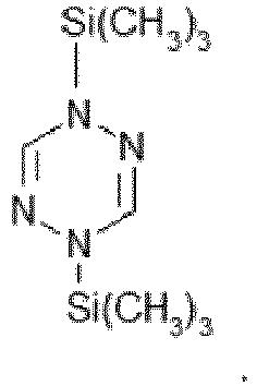
- The article XP055493427 entitled « Titanium-based molecular squares and rectangles: syntheses by self-assembly reactions of titanocene fragments and aromatic N-heterocycles », published in Chemistry- A European Journal, et al discloses a compound having the following formula:

- The present invention as claimed solves one or more problems of the prior art by providing a method of forming a layer on a substrate, the method comprising a deposition cycle including:
- a) contacting a substrate with a vapor of a first compound to form a first modified surface, the first compound having an atom in an oxidized state to form said first modified surface, said atom being selected from the group consisting of Cu, Ni, Cr, Mn, Fe, Co;
- b) contacting the first modified surface with an acid for a second predetermined pulse time to form a second modified surface; and
- c) contacting the second modified surface with a reducing agent for a third predetermined pulse time to reduce the atom to a zero oxidation state and to form a layer on the substrate, the reducing agent being 1,4-bis(trimethylsilyl)-1,4-dihydropyrazine.
- According to one embodiment, the atom is in a positive oxidation state of 1, 2, 3, 4, 5, or 6.
- The first compound can be selected from bis(dimethylamino-2-propoxy) copper (II) (Cu(dmap)2), bis(dimethylamino-2-propoxy) nickel (II) (Ni(dmap)2, bis(1,4-di-tert-butyldiazene) chromium(II) (Cr(dadtBu2)2), bis(1,4-di-tert-butyldiazene) manganese (II) (Mn(dadtBu2)2), bis(1,4-di-tert-butyldiazene) iron(II) (Fe(dadtBu2)2), bis(1,4-di-tert-butyldiazene) cobalt(II) (Co(dadtBu2)2) and bis(1,4-di-tert-butyldiazene) nickel(II) (Ni(dadtBu2)2).
- According to another embodiment, the substrate is additionally contacted with the vapor of the first compound having an atom in an oxidized state, the acid, and the vapor of a reducing agent during a plurality of additional deposition cycles.
- The substrate can be selected from SiH and Co when said first compound is Cu(dmap)2, Si when said first compound is Ni(Dmap)2, Ru when said first compound is Ni(Dmap)2 or Ni(dadtBu2)2, Pd when said first compound is Ni(Dmap)2, Cu when said first compound is Ni(dadtBu2)2, Ru or SiO2 when said first compound is Cr(dadtBu2)2, Ru or SiO2 when said first compound is Mn(dadtBu2)2, SiO2 when said first compound is Fe(dadtBu2)2, Ru or SiO2 when said first compound is Co(dadtBu2)2.
- The acid can be formic acid.
- The following figures are not according to the invention and are present for illustration purpose only:
Fig. 1 ,3 ,4 ,5 ,6 ,7 ,38 to 56 and63 to 69 . - Exemplary embodiments of the present invention will become more fully understood from the detailed description and the accompanying drawings, wherein:
-
FIGURE 1 provides additional examples of reducing agents; -
FIGURE 2A is a schematic flowchart illustrating an ALD deposition process using the bis(trimethylsilyl) six-membered ring systems of an embodiment of the invention; -
FIGURE 2B is a schematic flowchart illustrating an ALD deposition process using the bis(trimethylsilyl) six-membered ring systems of an embodiment of the invention; -
FIGURE 2C is a schematic flowchart illustrating an ALD deposition process using the bis(trimethylsilyl) six-membered ring systems of an embodiment of the invention; -
FIGURE 2D is a schematic illustration of an ALD deposition system used in an embodiment of the present invention; -
FIGURE 2E is a schematic cross-section of a vapor source containing the reducing agents; -
FIGURE 3 provides examples of acids that can be reacted with the compounds of formula I; -
FIGURE 4 provides X-ray diffraction spectra showing CuCl formed by the solution reductions of CuCl2 and CuCl2•H2O by 1,4-bis(trimethylsilyl)-2-methyl-1,4-cyclohexadiene; -
FIGURE 5 provides an X-ray diffraction spectrum showing copper metal formed by the solution reduction of CuCl2 to CuCl by 1,4-bis(trimethylsilyl)-2-methyl-1,4-cyclohexadiene , and the subsequent disproportionation to copper metal by ethylenediamine; -
FIGURE 6 provides a scanning electron micrograph of a copper film (~ 8 nm) on a ruthenium-coated (5 nm) SiO2 wafer; -
FIGURE 7 provides a cyclic voltammogram of pyrazine referenced to Ag/AgNO3; -
FIGURE 8 provides an X-ray diffraction spectrum showing copper metal formed by the solution reduction of Cu(tmhd)2 by 1,4-bis(trimethylsilyl)-1,4-dihydropyrazine; -
FIGURE 9 provides a cross-sectional SEM micrograph of a copper film on a SiH substrate formed from Cu(dmap)2; -
FIGURE 10 provides a top-down SEM micrograph of a copper film on Co/SiO2 formed from Cu(dmap)2; -
FIGURE 11 provides XPS survey scans of a 51 nm copper film deposited on SiH at 150 °C formed from Cu(dmap)2; -
FIGURE 12 provides an XPS high-resolution multiplex of the Cu 2p3 region of a film formed from Cu(dmap)2; -
FIGURE 13 provides a cross-sectional SEM micrograph of a nickel film on a Si(100) substrate formed from Ni(dmap)2; -
FIGURE 14 provides a cross-sectional SEM micrograph of a nickel film on a Ru/SiO2 substrate formed from Ni(dmap)2; -
FIGURE 15 provides XPS survey scans of a 32 nm nickel film deposited on Pd at 150 °C formed from Ni(dmap)2; -
FIGURE 16 provides an XPS high-resolution multiplex of the Ni 2p3 region of a film formed from Ni(dmap)2; -
FIGURE 17 provides a cross-sectional SEM micrograph of a chromium film on a Ru/SiO2 substrate formed from Cr(dadtBu2)2; -
FIGURE 18 provides a cross-sectional SEM micrograph of chromium film on a SiO2 substrate formed from Cr(dadtBu2)2; -
FIGURE 19 provides XPS survey scnas of a 124 nm thick chromium film deposited on thermal SiO2 at 225° C formed from Cr(dadtBu2)2; -
FIGURE 20 provides an XPS high-resolution multiplex of the Cr 2p3 region of a film formed from Cr(dadtBu2)2; -
FIGURE 21 provides a cross-sectional SEM micrograph of a manganese film on a Ru/SiO2 substrate formed from Mn(dadtBu2)2; -
FIGURE 22 provides a top-down SEM micrograph of a manganese film on a Ru/SiO2 substrate formed from Mn(dadtBu2)2; -
FIGURE 23 provides XPS survey scans of a 27 nm manganese film deposited on SiO2 at 225 °C formed from Mn(dadtBu2)2; -
FIGURE 24 provides an XPS high-resolution multiplex of the Mn 2p3 region of a film formed from Mn(dadtBu2)2; -
FIGURE 25 provides a cross-sectional SEM micrograph of an iron film on a thermal SiO2 substrate formed from Fe(dadtBu2)2; -
FIGURE 26 provides a top-down SEM micrograph of an iron film on thermal SiO2 formed from Fe(dadtBu2)2; -
FIGURE 27 provides XPS survey scans of a 35 nm thick iron film deposited on Ru/SiO2 at 225 °C formed from Fe(dadtBu2)2; -
FIGURE 28 provides an XPS high-resolution multiplex of the Fe 2p3 region of a film formed from Fe(dadtBu2)2; -
FIGURE 29 provides a cross-sectional SEM micrograph of a cobalt film on a Ru/SiO2 substrate formed from Co(dadtBu2)2; -
FIGURE 30 provides a top-down SEM micrograph of a cobalt film on a thermal SiO2 substrate formed from Co(dadtBu2)2; -
FIGURE 31 provides XPS survey scans of a 24 nm thick cobalt film deposited on Ru/SiO2 at 180 °C from Co(dadtBu2)2; -
FIGURE 32 provides an XPS high-resolution multiplex of the Co 2p3 region of a film formed from Co(dadtBu2)2; -
FIGURE 33 provides an X-ray diffraction spectrum of showing cobalt metal on a SiO2 substrate formed from Co(dadtBu2)2; -
FIGURE 34 provides a cross-sectional SEM micrograph of a nickel film on a Ru/SiO2 substrate formed from Ni(dadtBu2)2; -
FIGURE 35 provides a top-down SEM micrograph of a nickel film on a copper substrate formed from Ni(dadtBu2)2; -
FIGURE 36 : provides XPS survey scans of a 34 nm thick nickel film deposited on Ru/SiO2 at 180 °C from Ni(dadtBu2)2; -
FIGURE 37 : provides an XPS high-resolution multiplex of the Ni 2p3 region for a film formed from Ni(dadtBu2)2; -
FIGURE 38 provides X-ray diffraction (XRD) spectra for solution reaction precipitates formed from the reaction with titanium tetrachloride and CHD (e.g., formula IA) and titanium tetrachloride and DHP (e.g., formula IB); -
FIGURE 39A provides an SEM cross-section for an ALD film deposited on a platinum substrate from the reaction with titanium tetrachloride and CHD at 180° C; -
FIGURE 39B provides an SEM cross-section for an ALD film deposited on a silicon substrate with a thermal silicon oxide layer from the reaction with titanium tetrachloride and CHD at 180° C; -
FIGURE 39C provides an SEM cross-section for an ALD film deposited on a palladium substrate from the reaction with titanium tetrachloride and CHD at 180° C -
FIGURE 39D provides an SEM cross-section for an ALD film deposited on a cobalt substrate from the reaction with titanium tetrachloride and CHD at 180° C; -
FIGURE 40 provides XPS survey scans for an ALD film deposited on a platinum substrate from the reaction with titanium tetrachloride and CHD at 180° C; -
FIGURE 41 provides XPS multiplex scans for an ALD film deposited on a platinum substrate from the reaction with titanium tetrachloride and CHD at 180° C; -
FIGURE 42 provides XPS survey scans for ALD film deposited on a silicon substrate with a thermal silicon oxide layer from the reaction with titanium tetrachloride and CHD at 180° C; -
FIGURE 43 provides XPS multiplex scans for an ALD film deposited on silicon substrate with a thermal silicon oxide layer from the reaction with titanium tetrachloride and CHD at 180° C; -
FIGURE 44A provides an SEM cross-section for an ALD film deposited on a platinum substrate from the reaction with titanium tetrachloride and DHP; -
FIGURE 44B provides an SEM cross-section for an ALD film on a silicon substrate with a thermal silicon oxide layer from the reaction with titanium tetrachloride and DHP; -
FIGURE 44C provides an SEM cross-section for an ALD film on a palladium substrate from the reaction with titanium tetrachloride and DHP; -
FIGURE 44D provides an SEM cross-section for an ALD film on a cobalt substrate from the reaction with titanium tetrachloride and DHP; -
FIGURE 45 provides X-ray diffraction (XRD) spectra for ALD films formed from the reaction with titanium tetrachloride and DHP on a platinum substrate and a silicon oxide substrate; -
FIGURE 46 provides Energy-dispersive X-ray (EDS) spectra for ALD films formed from the reaction with titanium tetrachloride and DHP on a platinum substrate and a silicon oxide substrates; -
FIGURE 47 provides XPS survey scans for an ALD film deposited on a platinum substrate from the reaction with titanium tetrachloride and DHP at 100° C; -
FIGURE 48 provides XPS multiplex scans for an ALD film deposited on a platinum substrate from the reaction with titanium tetrachloride and DHP at 100° C; -
FIGURE 49 provides XPS survey scans for an ALD film deposited a silicon substrate with a thermal silicon oxide layer from the reaction with titanium tetrachloride and DHP at 100° C; -
FIGURE 50 provides XPS multiplex scans for an ALD film deposited on a silicon substrate with a thermal silicon oxide layer from the reaction with titanium tetrachloride and DHP at 100° C; -
FIGURE 51A provides a SEM cross-section of an aluminum film deposited on a silicon substrate with a thermal silicon oxide layer from trimethylaluminum and DHP at 180° C; -
FIGURE 51B provides a SEM cross-section of an aluminum film deposited on a cobalt-coated silicon substrate from trimethylaluminum and DHP at 180° C; -
FIGURE 52 provides XPS survey scans for an ALD film deposited on a cobalt-coated silicon substrate from trimethylaluminum and DHP at 180° C; -
FIGURE 53 provides XPS multiplex scans for an ALD film deposited on a cobalt-coated silicon substrate from trimethylaluminum and DHP at 180° C; -
FIGURE 54A provides an SEM cross-section for an ALD film deposited on a platinum substrate from antimony trichloride and DHP at 180° C; -
FIGURE 54B provides an SEM top-down view for an ALD film deposited on a platinum substrate from antimony trichloride and DHP at 180° C; -
FIGURE 54C provides an SEM cross-section for an ALD film deposited on a palladium substrate from antimony trichloride and DHP at 180° C; -
FIGURE 54D provides an SEM top-down view for an ALD film deposited on a palladium substrate from antimony trichloride and DHP at 180° C; -
FIGURE 55 provides XPS survey scans for an ALD film deposited on a palladium substrate from antimony trichloride and DHP at 180° C; -
FIGURE 56 provides XPS multiplex scans for an ALD film deposited on a palladium substrate from antimony trichloride and DHP at 180° C; -
FIGURE 57 provides sheet resistances for cobalt films grown on Ru, Pt, and Pd substrates; -
FIGURE 58 provides growth rates and sheet resistances versus temperature for cobalt films on a Ru substrate; -
FIGURE 59 provides SEM cross-sectional micrographs of cobalt films on Ru substrates; -
FIGURE 60 provides SEM cross-sectional micrographs of cobalt films on Ru substrates; -
FIGURE 61 provides SEM top-down view micrographs of cobalt films on Ru substrates; -
FIGURE 62 provides SEM top-down view micrographs of cobalt films on Ru substrates; -
FIGURE 63 provides TEM images of methanol-washed un-capped Si particles; -
FIGURE 64 provides an EDS analysis of methanol-washed Si particles; -
FIGURE 65 provides a PXRD spectrum of Si particles; -
FIGURE 66 provides a TEM image and size distribution of Si particles; -
FIGURE 67 provides TEM images of Si particles in which methanol was added before reaction with 1-octanol; -
FIGURE 68 provides the PXRD spectrum of the formed Ge particles; and -
FIGURE 69 provides a TEM image of the Ge nanoparticles. Since the samples were handled outside after isolation, it is believed that the lighter area around the nanoparticles may be due to the surface oxidation. - Reference will now be made in detail to presently preferred compositions, embodiments, and methods of the present invention which constitute the best modes of practicing the invention presently known to the inventors. The Figures are not necessarily to scale. However, it is to be understood that the disclosed embodiments are merely exemplary of the invention that may be embodied in various and alternative forms. Therefore, specific details disclosed herein are not to be interpreted as limiting, but merely as a representative basis for any aspect of the invention and/or as a representative basis for teaching one skilled in the art to variously employ the present invention.
- Except in the examples, or where otherwise expressly indicated, all numerical quantities in this description indicating amounts of material or conditions of reaction and/or use are to be understood as modified by the word "about" in describing the broadest scope of the invention. Practice within the numerical limits stated is generally preferred. Also, unless expressly stated to the contrary: percent, "parts of," and ratio values are by weight; "R" groups include H, C1-10 alkyl, C2-10 alkenyl, C6-14 aryl (e.g., phenyl, halo, or C4-14 heteroaryl; the description of a group or class of materials as suitable or preferred for a given purpose in connection with the invention implies that mixtures of any two or more of the members of the group or class are equally suitable or preferred; description of constituents in chemical terms refers to the constituents at the time of addition to any combination specified in the description, and does not necessarily preclude chemical interactions among the constituents of a mixture once mixed; the first definition of an acronym or other abbreviation applies to all subsequent uses herein of the same abbreviation and applies mutatis mutandis to normal grammatical variations of the initially defined abbreviation; and, unless expressly stated to the contrary, measurement of a property is determined by the same technique as previously or later referenced for the same property.
- It must also be noted that, as used in the specification and the appended claims, the singular form "a," "an," and "the" comprise plural referents unless the context clearly indicates otherwise. For example, reference to a component in the singular is intended to comprise a plurality of components.
-
- "ALD" is atomic layer deposition.
- "CVD is chemical vapor deposition.
- "RT" means "room temperature."
- "s" means "seconds."
- "THF" means "tetrahydrofuran."
- "DME" means "1,2-dimethoxyethane."
- "CHD" means 1,4-bis(trimethylsilyl)-2-methyl-1,4-cyclohexadiene.
- "DHP" means 1,4-bis(trimethylsilyl)-1,4-dihydropyrazine.
- "dad" means diazadiene.
- "dadtBu2" means "1,4-di-tert-butyldiazadiene."
- "XPS" means "X-ray photoelectron spectroscopy."
- "SEM" means "scanning electron microscopy."
- "XRD" means "X-ray diffraction."
- "acac" is acetylacetonate.
- "Cp" is cyclopentadienyl.
- "dmap" is 1-dimethylamino-2-methyl-2-propoxy.
- "en" is ethylene diamine.
- "Et" is ethyl.
- "EtCp" is ethylcyclopentadienyl.
- "Et2amd" is N, N'-diethylacetamidinate.
- "Et2fmd" is N,N'-diethylformamidinate.
- "hfac" is 1,1,1,5,5,5-hexafluoro-acetylacetonate.
- "iPr2amd" is N, N'-diisopropylacetamidinate.
- "iPr2fmd" is N,N'-diisopropylformamidinate.
- "iPrCp" is isopropylcyclopentadienyl.
- "Me" is methyl.
- "Me2amd" is N, N'-dimethylacetamidinate.
- "Me2fmd" is N,N'-dimethylformamidinate.
- "Mes" is 2,4,6-Me3C6H2 or mesityl.
- "MeCp" is methylcyclopentadienyl.
- "Me5Cp" is pentamethylcyclopentadienyl.
- "Me2fmd" is N,N'-dimethylformamidinate.
- "Me2bmd" is N-N'-dimethylbutyramidinate.
- "Me2pmd" is N, N'-dimethylpropionamidinate.
- "mmp" is 1-methoxy-2-methyl-2-propoxy.
- "OtPe" is tert-pentoxy.
- "od" is octane-2 4-dionate.
- "OiPr" is isopropoxy.
- "OtBu" is tert-butoxy.
- "OEt" is ethoxy.
- "tBu2amd" is N, N'-di-tert-butylacetamidinate.
- "tBuEtamd" is N-tert-butyl-N'-ethylacetamidinate.
- "tBuEtpmd" is N-tert-butyl-N'-ethyl-propionamidinate.
- "tBuEtbmd" is N-tert-butyl-N'-ethylbutyramidinate.
- "thd" is 2,2,6,6-tetramethyl- heptane-3,5-dionate.
- "TEM" is transmission electron microscopy.
- "PXRD" is powder X-ray diffraction.
- "EDS" is Energy-dispersive X-ray spectroscopy.
- The term "standard electrode potential" means the electrical potential (i.e., the voltage developed) of a reversible electrode at standard state in which solutes are at an effective concentration of 1 mol/liter, the activity for each pure solid, pure liquid, or for water (solvent) is 1, the pressure of each gaseous reagent is 1 atm., and the temperature is 25 °C. Standard electrode potentials are reduction potentials.
- In a further refinement, a method of forming a metal film by an ALD process is provided.
The method comprises a deposition cycle which includes contacting the substrate with vapor of a first compound having an atom in an oxidized state as set forth above such that at least a portion of the vapor of the first compound adsorbs or reacts with a substrate surface to form a modified surface.
The deposition cycle further includes contacting the modified surface with a vapor of the reducing agents set forth above to react and form at least a portion of the metal film.
Typically, the first compound having an atom in an oxidized state is contacted with the reducing agent at a temperature from about 50 to 400 ° C.
The present reaction is used in an ALD process as set forth below. - With reference to
Figure 2A , a method for forming a layer by an ALD process is schematically illustrated. In step a),substrate 10 is contacted with a vapor G1 of a first compound having an atom in an oxidized state to form a first modifiedsurface 12. The atom in an oxidized state is selected from the group consisting Groups 2-12 of the Periodic Table, the lanthanides, As, Sb, Bi, Te, Si, Ge, Sn, and Al. In particular, the first compound is as set forth above. In step b) the first modifiedsurface 12 is contacted with a reducing agent G2 for a predetermined pulse time to formlayer 14 on thesubstrate 10. The details of the reducing agent are as set forth above. Purging steps P1 and P2 are performed after steps a) and b), respectively. Loop L indicates that steps a), P1), b), and P2) are repeated a plurality of times in order to build up afinal layer 16 of predetermined thickness monolayer by monolayer. Additional details of this ALD process are set forth below. - With reference to
Figure 2B , a method for forming a layer by an ALD process is schematically illustrated. In step a),substrate 10 is contacted with a vapor G1 of a first compound having an atom in an oxidized state to form a first modifiedsurface 12. The atom in an oxidized state is selected from the group consisting of Groups 2-12 of the Periodic Table, the lanthanides, As, Sb, Bi, Te, Si, Ge, Sn, and Al In particular, the first compound is as set forth above. In step b), the first modifiedsurface 12 is contacted with an acid A1 for a second predetermined pulse time to form a second modified surface 12'. In step c), the second modified surface 12' is contacted with a reducing agent G2 for a third predetermined pulse time to formlayer 14 on the substrate. Purging steps P1, P2, and P3 are performed after steps a), b), and c), respectively. Loop L indicates that steps a), P1), b), P2), c), and P3 are repeated a plurality of times in order to build up afinal layer 16 of predetermined thickness monolayer by monolayer. The details of the reducing agent are as set forth above. Additional details of this ALD process are set forth below. - With reference to
Figure 2D ,deposition system 20 includesreaction chamber 22,substrate holder 24, andvacuum pump 26. Typically, the substrate is heated viaheater 28. The method has a deposition cycle comprising contactingsubstrate 30 with a vapor of the first compound having an atom in an oxidized state as set forth above. In particular, the vapor is introduced fromprecursor source 32 intoreaction chamber 22 for a predetermined pulse time. The pulse time is controlled viacontrol valve 34. At least a portion of the vapor of the first compound modifies (e.g, adsorbs or reacts with)substrate surface 36 to form a modified surface. The method further comprises contacting the modified surface with a vapor of the reducing agent as set forth above fromsource 40 for a predetermined pulse time controlled byvalve 42. - In a variation of the present embodiment, the method further comprises removing at least a portion of the vapor of the first compound that is lingering in the gas phase (i.e., has not adsorbed or reacted with the substrate) from the vicinity of the substrate before introducing the vapor of the reducing agent and removing at least a portion of the vapor of the reducing agent from the vicinity of the substrate. The metal-containing compound and the reducing agent are removed in purging steps by introducing a purge gas from
purge source 44 intoreaction chamber 22 for a predetermined purge time. The purge time is controlled bycontrol valve 46. - In another variation, the method further includes at least one additional deposition cycle comprising sequentially contacting the substrate with the vapor of the first compound and then the vapor of the reducing agent. In some refinements, the substrate is contacted for a plurality of additional deposition cycles. For example, the substrate may be contacted with from 1 to several thousand deposition cycles depending on the thickness of the film desired. In particular, the substrate is contacted with the vapor of the first compound having an atom in an oxidized state and then the vapor of the reducing agent for 1 to 5000 deposition cycles. In another refinement, the substrate is contacted with the vapor of the first compound having an atom in an oxidized state and then the vapor of the reducing agent for 10 to 2000 deposition cycles. In still another refinement, the substrate is contacted with the vapor of the first compound having an atom in an oxidized state and then the vapor of the reducing agent for 20 to 1000 deposition cycles.
- The system of
Figure 2D uses asource 40 for providing the vapor of a reducing agent.Figure 2E provides a schematic cross-section of such a vapor source. Reducingagent source 40 includesvessel 60 and reducingagent 62 which is contained within and held by the vessel. Reducingagent 62 is one or more of the reducing agents set forth above. In particular, reducingagent 62 is described by IA, IB, IIA, IIB, IIC, and IID. In a refinement, at least a portion of the reducing agent is in the liquid phase.Valve 64 is attached tovessel 60.Valve 64 prevents escape of the reducing agent when the valve is closed and allows escape (i.e., passage into theALD reaction chamber 22 through output conduit 66) of the reducing agent when the valve is opened. In a refinement,source 40 is a bubbler having aninput conduit 70 for flowing a gas intovessel 60 and out ofoutput conduit 66 thereby transferring the reducing agent.Valve 72 allowsinput conduit 70 to be opened and closed. In a refinement, in a refinement reducingagent source 40 includes fitting 74 positioned outside of and in fluid communication withvalve 64. Optional, fitting 76 is position outside of and in fluid communication withvalve 72.Fittings - In another embodiment, a system and method of forming a metal-containing film is provided. With reference to
Figure 2D , the vapor of the first compound having an atom in an oxidized state is introduced fromprecursor source 32 intoreaction chamber 22 for a first predetermined pulse time. The first predetermined pulse time should be sufficiently long that available binding sites on the substrate surface (coated with metal layers or uncoated) are saturated (i.e., metal-containing compound attached). Typically, the first predetermined pulse time is from 1 second to 20 seconds. The first predetermined pulse time is controlled viacontrol valve 34. At least a portion of the vapor of the metal-containing compound modifies (e.g, adsorbs or reacts with)substrate surface 36 to form a first modified surface.Reaction chamber 22 is then purged with an inert gas frompurge source 44 for a first purge time. The first purge time is sufficient to remove the metal-containing compound fromreaction chamber 22 and is typically from 0.5 seconds to 2 minutes. - In the next reaction step of the deposition cycle, an acid such as formic acid is then introduced from
acid source 50 intoreaction chamber 22 for a second predetermined pulse time. Examples of other suitable acids are provided inFigure 3 . InFigure 3 , R20 is H (i.e., hydride), C1-8 alkyl, C6-12 aryl, or C1-8 fluoroalkyl, X is N3 -, NO3 -, halide (e.g., Cl, F, Br), and o is an integer from 1 to 6. In a refinement, R20 is hydride, C1-4 alkyl, C6-10 aryl, or C1-4 fluoroalkyl, X is N3 -, NO3 -, halide (e.g., Cl, F, Br), and n is an integer from 1 to 6. Examples of useful alkyl groups include, but are not limited to, methyl, ethyl, n-propyl, isopropyl, n-butyl, t-butyl, isobutyl, sec-butyl, and the like. Examples of useful aryl groups include, but are not limited to, phenyl, tolyl, naphthyl, and the like. The second predetermined pulse time is controlled viavalve 52 and should be sufficiently long that available binding sites on the first modified substrate surface are saturated and a second modified surface is formed. Typically, the second predetermined pulse time is from 0.1 second to 20 seconds.Reaction chamber 22 is then purged with an inert gas for a second purge time (typically, 0.5 seconds to 2 minutes as set forth above). - In the final reaction step of the deposition cycle, a reducing agent as set forth above is then introduced from reducing
agent source 40 intoreaction chamber 22 for a third predetermined time controlled byvalve 42. The third predetermined pulse time should be sufficiently long that available binding sites on the second modified substrate surface are saturated, with a metal layer being formed thereon. Typically, the third predetermined pulse time is from 0.1 second to 20 seconds.Reaction chamber 22 is then purged with an inert gas for a third purge time (typically, 0.5 second to 2 minutes as set forth above). - During film formation by the method of the present embodiment, the substrate will be at a temperature suitable to the properties of the chemical precursor(s) and film to be formed. In a refinement of the method, the substrate is set to a temperature from about 0 to 1000 °C. In another refinement of the method, the substrate has a temperature from about 50 to 450 °C. In another refinement of the method, the substrate has a temperature from about 100 to 250 °C. In still another refinement of the method, the substrate has a temperature from about 150 to 400 °C. In another refinement of the method, the substrate has a temperature from about 200 to 300 °C.
- Similarly, the pressure during film formation is set at a value suitable to the properties of the chemical precursors and film to be formed. In one refinement, the pressure is from about 10-6 Torr to about 760 Torr. In another refinement, the pressure is from about 0.1 millitorr to about 10 Torr. In still another refinement, the pressure is from about 1 to about 100 millitorr. In yet another refinement, the pressure is from about 1 to 20 millitorr.
- Pulse times and purge times also depend on the properties of the chemical precursors and the geometric shape of the substrates. Thin film growth on flat substrates uses short pulse and purge times, but pulse and purge times in ALD growth on 3-dimensional substrates can be very long. Therefore, in one refinement, pulse times and purge times are each independently from about 0.0001 to 200 seconds. In another refinement, pulse and purge times are each independently from about 0.1 to about 10 seconds.
- With reference to
Figure 2B , another variation for forming a metal film is schematically illustrated. In step a),substrate 10 is contacted with a vapor of a metal-containing compound G1 having formula III or IV to form a first modifiedsurface 12 on thesubstrate 10. In step b), the first modifiedsurface 12 is then contacted with a vapor of the activating compound A1 to form a second modified surface 12'. In step c), the second modified surface 12' is then contacted with the vapor of a reducing agent G2 to form at least a portion of a metal film on the substrate. Examples of suitable reducing agents include, but are not limited to, hydrazine, hydrazine hydrate, alkyl hydrazines, 1,1-dialkylhydrazines, 1,2-dialkylhydrazines, H2, H2 plasma, ammonia, ammonia plasma, silanes, disilanes, trisilanes, germanes, diborane, formalin, amine borane, dialkyl zinc, alkyl aluminum, alkyl gallium, alkyl indium complexes, and other plasma-based gases, and combinations thereof. Additional examples of reducing agents include the bis(trimethylsilyl) six-membered ring systems and related compounds as set forth above. - With reference to
Figure 2D ,deposition system 20 includesreaction chamber 22,substrate holder 24, andvacuum pump 26. Typically, the substrate is heated viaheater 28. The method has a deposition cycle comprising contactingsubstrate 30 with a vapor of the compound having formula III or IV or the variations of these compounds as set forth above. In particular, the vapor is introduced fromprecursor source 32 intoreaction chamber 22 for a predetermined pulse time. The pulse time is controlled viacontrol valve 34. At least a portion of the vapor of the compound having formula III or IV modifies (e.g, adsorbs or reacts with)substrate surface 36 to form a modified surface. The method further comprises contacting the modified surface with a vapor of the activating compound (e.g., C1-5 organic acids such as formic acid and C1-8 diketone) as set forth above fromsource 50 for a predetermined pulse time to form a metal layer or metal-containing layer. - In a variation of the present embodiment, the method further comprises removing at least a portion of the vapor of the compound having formula III or IV that is lingering in the gas phase (i.e., has not adsorbed or reacted with the substrate) from the vicinity of the substrate before introducing the vapor of the activating compound and removing at least a portion of the vapor of the activating compound from the vicinity of the substrate. The metal-containing compound and the activating compound are removed in purging steps by introducing a purge gas from
purge source 44 intoreaction chamber 22 for a predetermined purge time. The purge time is controlled bycontrol valve 46. - In another variation, the method further includes at least one additional deposition cycle comprising sequentially contacting the substrate with the vapor of the compound having formula III or IV and then the vapor of the reducing agent. In some refinements, the substrate is contacted for a plurality of additional deposition cycles. For example, the substrate may be contacted with from 1 to several thousand deposition cycles depending on the thickness of the film desired. In particular, the substrate is contacted with the vapor of the compound having formula III or IV and then the vapor of the activating compound for 1 to 5000 deposition cycles. In another refinement, the substrate is contacted with the vapor of the compound having formula III or IV and then the vapor of the activating compound for 10 to 2000 deposition cycles. In still another refinement, the substrate is contacted with the vapor of the compound having formula III or IV and then the vapor of the activating compound for 20 to 1000 deposition cycles.
- In another embodiment, a method of forming a metal-containing film is provided. With reference to
Figure 2D , the vapor of the compound having formula III or IV is introduced fromprecursor source 32 intoreaction chamber 22 for a first predetermined pulse time. The first predetermined pulse time should be sufficiently long that available binding sites on the substrate surface (coated with metal layers or uncoated) are saturated (i.e., metal-containing compound attached). Typically, the first predetermined pulse time is from 1 second to 20 seconds. The first predetermined pulse time is controlled viacontrol valve 34. At least a portion of the vapor of the metal-containing compound modifies (e.g, adsorbs or reacts with)substrate surface 36 to form a first modified surface.Reaction chamber 22 is then purged with an inert gas frompurge gas source 44 for a first purge time. The first purge time is sufficient to remove the metal-containing compound fromreaction chamber 22 and is typically from 0.5 seconds to 2 minutes. - In the next reaction step of the deposition cycle, the activating compound (e.g., C1-5 organic acids such as formic acid and C1-8 diketone) as set forth above is then introduced from
source 50 intoreaction chamber 22 for a second predetermined pulse time. The second predetermined pulse time is controlled viavalve 52 and should be sufficiently long that available binding sites on the first modified substrate surface are saturated and a second modified surface is formed. Typically, the second predetermined pulse time is from 0.1 second to 20 seconds. The second predetermined pulse time is controlled viacontrol valve 32.Reaction chamber 12 is then purged with an inert gas for a second purge time (typically, 0.5 seconds to 2 minutes as set forth above). - In the final reaction step of the deposition cycle, a reducing agent having formula IA or IB or the derivatives thereof as set forth above is then introduced from reducing
agent source 40 intoreaction chamber 22 for a third predetermined time controlled byvalve 42. The third predetermined pulse time should be sufficiently long that available binding sites on the second modified substrate surface are saturated, with a metal layer being formed thereon. Typically, the third predetermined pulse time is from 0.1 second to 20 seconds.Reaction chamber 22 is then purged with an inert gas for a third purge time (typically, 0.5 seconds to 2 minutes as set forth above). - In a variation of the present embodiment, the method further includes at least one additional deposition cycle comprising sequentially contacting the substrate with the vapor of the compound having formula III or IV and then the vapor of the reducing agent. In some refinements, the substrate is contacted for a plurality of additional deposition cycles. For example, the substrate may be contacted with from 1 to several thousand deposition cycles depending on the thickness of the film desired. In particular, the substrate is contacted with the vapor of the compound having formula III or IV and then the vapor of the activating compound for 1 to 5000 deposition cycles. In another refinement, the substrate is contacted with the vapor of the compound having formula III or IV and then the vapor of the activating compound for 10 to 2000 deposition cycles. In still another refinement, the substrate is contacted with the vapor of the compound having formula III or IV and then the vapor of the activating compound for 20 to 1000 deposition cycles.
- During film formation by the methods set forth above, the substrate will be at a temperature suitable to the properties of the chemical precursor(s) and film to be formed. In a refinement of the method, the substrate is set to a temperature from about 0 to 1000 °C. In another refinement of the method, the substrate has a temperature from about 50 to 450 °C. In another refinement of the method, the substrate has a temperature from about 100 to 250 °C. In still another refinement of the method, the substrate has a temperature from about 150 to 400 °C. In another refinement of the method, the substrate has a temperature from about 200 to 300 °C.
- Similarly, the pressure during film formation is set at a value suitable to the properties of the chemical precursors and film to be formed. In one refinement, the pressure is from about 10-6 Torr to about 760 Torr. In another refinement, the pressure is from about 0.1 millitorr to about 10 Torr. In still another refinement, the pressure is from about 1 to about 100 millitorr. In yet another refinement, the pressure is from about 1 to 20 millitorr.
- Pulse times and purge times also depend on the properties of the chemical precursors and the geometric shape of the substrates. Thin film growth on flat substrates uses short pulse and purge times, but pulse and purge times in ALD growth on 3-dimensional substrates can be very long. Therefore, in one refinement, pulse times and purge times are each independently from about 0.0001 to 200 seconds. In another refinement, pulse and purge times are each independently from about 0.1 to about 10 seconds.
- All experiments employed the use of anhydrous reagents and solvents, obtained from Sigma Aldrich. Syntheses of CHD and DHP were carried out using Schlenk line techniques, following previously referenced literature procedures contained in
U.S. Pat. Appl. No. 13930471 filed June 28, 2013 - 1,4-bis(trimethylsilyl)-1,4-dihydropyrazine was prepared on a 40 g scale following a literature procedure (Sulzbach, R. A.; Iqbal, A. F. M. Angew. Chem. Int. Ed. Engl. 1971, 10, 127). The air-sensitive, yellow solid was purified by sublimation at 80 °C /0.05 Torr. Preparative sublimation of the product yielded 97.1 % recovery with no residue. The thermal decomposition temperature was determined to be greater than 265 °C.

- Solution reactions were conducted with a variety of metal salts in THF. Upon refluxing with DHP, precipitate formation was observed from Cu, Ni, Co, Fe, Zn, and Cr salts (Table 3). Copper precipitate was observed as regions of copper-colored film on the flask and metallic flakes in solution, while cobalt and iron precipitated out as the ferromagnetic metals, sticking to the stir bar. The precipitate resulting from the reaction of copper bis(2,2,6,6-tetramethyl-3,5-heptanedionate) [Cu(tmhd)2] with DHP was identified as copper metal by XRD (
Figure 8 ).Table 3: Reaction matrix of metal salts with DHP ML2 THF Reaction Reflux Reaction solution → Precipitate Temp Time (min) Temp Time (min) Cu(dmap)2 50 ml RT 15 65 ° C 60 Cu flakes; Cu & green residue on flask Cu(tmhd)2 70 ml RT 30 65 °C 95 Cu & green flakes; Cu & purple residue on flask NiCl 2 50 ml RT 15 65 ° C 70 Tan powder CoCl 2 40 ml RT 35 65 ° C 60 Dark green powder at RT (sticks to stir bar) FeCl2 60 ml RT 35 65 ° C 60 Film on flask; black powder (sticks to stir bar) ZnCl2 75 ml RT 15 65 ° C 60 Few metallic flakes → white precipitate after about 3 days CrCl 2 70 ml RT 23 65 ° C 60 Silver-colored flakes → grey suspension MnCl 2 50 ml RT 15 65 ° C 60 None - A binary process using Cu(dmap)2 and DHP at 150 °C failed to produce films on any substrates (Si(100), SiH, thermal SiO2, Cu, Pt, Pd, TiN, and Ru/SiO2, Co/SiO2). A three-step process was subsequently attempted, whereby formic acid was used to produce the metal formate, which was then reduced to copper metal by 1,4-bis(trimethylsilyl)-1,4-dihydropyrazine. Subsequent applications of this general approach used numerous metal precursors, including Cu and Ni(dmap)2 and
various metal 1,4-di-tert-butyldiazadiene complexes [M(dadtBu2)2]. Each deposition cycle consisted of a precursor pulse (3.0 s for M(dmap)2 and 6.0 s for M(dadtBu2)2), a 5.0 s purge, a 0.2 s pulse of formic acid, a 5.0 s purge, a 1.0 s pulse of DHP , and a final 10.0 s purge. Delivery temperatures were maintained at 100 °C and 150 °C for M(dmap)2 and M(dadtBu2)2 precursors, respectively. Delivery temperatures were maintained at 70 °C and 21 °C for DHP and formic acid, respectively. Selected films from each deposition were characterized by SEM, XRD, and XPS as provided byFigures 9-37 . - TiCl4 was reacted with a 2.5 molar excess of CHD in toluene. Upon addition of the TiCl4 to the CHD solution, the mixture turned a dark rust-brown color with a dark precipitate. The mixture was stirred at ambient temperature for ~ 24 hrs. The solvent was removed under vacuum using a hot water bath. XRD analysis of the precipitate powder showed the major reflection of Ti metal (2θ = 38.4°,
Figure 38 ). - TiCl4 was reacted with a 2.6 molar excess of DHP in toluene. TiCl4 dissolved in toluene yielding a clear bright orange-colored solution. Upon addition of DHP, the solution immediately turned black with a very dark green/black precipitate. The mixture was stirred for ~ 24 hrs at ambient temperature. The solvent was removed under vacuum using a hot water bath. A small peak in the XRD spectrum matched that for the major reflection of Ti metal (2θ = 38.48,
Figure 38). Figure 38 provides XRD patterns for solution reaction precipitates formed from the reaction with TiCl4 and CHD and TiCl4 and DHP. The spectra show peaks corresponding to titanium metal, thereby verifying the formation of titanium metal in the zero oxidation state. - DHP completely dissolved in 40 mL of toluene, yielding a yellow solution. SiCl4 was directly added to the DHP solution, immediately producing a very faint white cloudiness near the bottom of the flask. The mixture was stirred at ambient temperature for ~ 72 hrs. A white precipitate was allowed to settle to the bottom of the flask. The solvent was removed under vacuum using a hot water bath. The yellow solution became increasingly dark as the solvent was removed; approximately 2-3 mL of liquid remained that would not evaporate. The remaining dark yellow slurry immediately turned brown upon air exposure. XRD analysis of the powder did not show any identifiable reflections.
- Titanium film growth was demonstrated using TiCl4 + CHD. Each cycle consisted of a 0.2 s pulse of TiCl4, a 15.0 s purge, a 1.0 s pulse of CHD, and a 10.0 s purge. The TiCl4 bubbler was maintained at 20 °C and the reaction chamber was held at 180 °C. The temperature of the solid state booster for CHD delivery was set to 75 °C. After 1,000 cycles, definitive films were observed on Pd, Pt, and SiO2 with growth rates of approximately 0.09 Å/cycle, 0.15 Å/cycle, and 0.08 Å/cycle, respectively. Discontinuous (island-type) growth was observed by SEM on the Co substrate. Faint films were observed on the Ru and Cu substrates; their presence was confirmed by SEM analysis.
- As used herein for the ALD experiments, platinum substrates consist of silicon substrates with a thermal oxide over coated with a platinum layer. Palladium substrates consist of silicon substrates with a thermal oxide over coated with a palladium layer. Cobalt substrates consist of silicon substrates with a thermal oxide over coated with a cobalt layer. It should be appreciated that SEM cross-sections are not able to distinguish the metal coating the substrate and the ALD film deposited thereon.
-
Figure 39A provides an SEM cross-section for an ALD film deposited on a platinum substrate from the reaction with TiCl4 and CHD at 180° C. From the micrograph, the combined platinum and titanium thickness is about 25 nm with an approximate platinum layer thickness of about 14 to 18 nm and a titanium layer thickness from 7 to 11 nm.Figure 39B provides an SEM cross-section for an ALD film deposited on a silicon substrate with a thermal silicon oxide layer from the reaction with TiCl4 and CHD at 180° C. From the micrograph, the titanium layer thickness is about 8 nm.Figure 39C provides an SEM cross-section for an ALD film deposited on a palladium substrate from the reaction with titanium tetrachloride and CHD at 180° C. From the micrograph, the combined palladium and titanium thickness is about 29 nm with an approximate palladium layer thickness of about 12 to 14 nm and a titanium layer thickness from 15 to 17 nm.Figure 39D provides an SEM cross-section for an ALD film deposited on a cobalt substrate from the reaction with titanium tetrachloride and CHD at 180° C. From the micrograph, the combined cobalt and titanium thickness is about 11 nm with an approximate cobalt layer thickness of about 6 to 10 nm and titanium layer thickness of about 1 to 5 nm. -
Figures 40 and41 respectively show XPS survey scans and XPS multiplex scans for an 8 nm ALD film deposited on a platinum substrate by reacting TiCl4 and CHD at 180 C. The scans confirm the presence of a titanium-containing film.Figures 42 and43 respectively show XPS survey scans and XPS multiplex scans for an 8 nm ALD film deposited on a silicon oxide coated silicon substrate by reacting TiCl4 and CHD at 180 C. The scans confirm the presence of a titanium-containing film. - Titanium film growth was demonstrated using TiCl4 + DHP. Each cycle consisted of a 0.2 s pulse of TiCl4, a 15.0 s purge, a 1.0 s pulse of DHP, and a 10.0 s purge. The TiCl4 bubbler was maintained at 20 °C and the reaction chamber was held at 100 °C. The temperature of the solid state booster for DHP delivery was set to 75 °C. After 3,000 cycles, definitive film growth was achieved on Pd, Pt, TiN, Co, Cu, Ru, Si(100), and SiO2. Average approximate growth rates were determined by SEM analysis: Pd (0.04 Å/cycle), Pt (0.11 Å/cycle), TiN (0.04 Å/cycle), Co (0.13 Å/cycle), Cu (0.11 Å/cycle), Ru (0.08 Å/cycle), Si (0.11 Å/cycle), and SiO2 (0.12 Å/cycle).
-
Figure 44A provides an SEM cross-section for an ALD film deposited on a platinum substrate from the reaction with titanium tetrachloride and DHP. From the micrograph, the combined platinum and titanium thickness is about 48 nm with an approximate platinum layer thickness of about 14 to 18 nm and a titanium layer thickness from 30 to 34 nm.Figure 44B provides an SEM cross-section for an ALD film on a silicon substrate with a thermal silicon oxide layer from the reaction with titanium tetrachloride and DHP. From the micrograph, the titanium layer thickness is about 35 nm.Figure 44C provides an SEM cross-section for an ALD film on a palladium substrate from the reaction with titanium tetrachloride and DHP. From the micrograph, the combined palladium and titanium thickness is about 24 nm with an approximate palladium layer thickness of about 12 to 14 nm and a titanium layer thickness of about 10 to 12 nm.Figure 44D provides an SEM cross-section for an ALD film on a cobalt substrate from the reaction with titanium tetrachloride and DHP. From the micrograph, the combined cobalt and titanium thickness is about 48 nm with an approximate titanium layer thickness of about 6 to 10 nm and a titanium layer thickness of about 38 to 42 nm. -
Figure 45 provides X-ray diffraction (XRD) spectra for ALD films formed from the reaction with TiCl4 and DHP on platinum substrates and silicon oxide substrates. It should be noted that the major Ti reflection appears on the Pt substrate as a minor component (2θ = 38.48°) and the major TiO2 reflection appears on the SiO2 substrate as a minor component (2θ = 44.67°). The thicknesses of the titanium films are about 30 to 35 nm.Figure 46 provides EDS spectra for ALD films formed from the reaction with TiCl4 and DHP on platinum substrates and silicon oxide substrates. The oxide film gradually changes in oxidation state from TiO2 → Ti2O3 → TiO → (by XPS analysis). It is hypothesized that oxide growth is controlled by oxygen diffusion through the existing oxide film (Brunette, D.M.; Tengvall, P.; Textor, M.; Thomsen, P. Titanium in Medicine; Springer, 2001; pp. 178-182). Finally, the thickness of the interfacial gradient layer is 39 ± 2 nm for polished commercially prepared titanium by RBS analysis (Brunette, D.M.; Tengvall, P.; Textor, M.; Thomsen, P. Titanium in Medicine; Springer, 2001; pp. 178-182).Figures 47 and48 , respectively, show XPS survey scans and XPS multiplex scans for a 34 nm ALD film deposited on a platinum substrate by reacting TiCl4 and DHP at 100 C. The scans confirm the presence of a titanium-containing film.Figures 49 and50 , respectively, show XPS survey scans and XPS multiplex scans for a 35 nm ALD film deposited on a silicon oxide coated silicon substrate by reacting TiCl4 and DHP at 100 C. The scans confirm the presence of a titanium-containing film. - Aluminum film growth was demonstrated using Al(CH3)3 and DHP. Each cycle consisted of a 0.1 s pulse of Al(CH3)3, a 8.0 s purge, a 1.0 s pulse of DHP, and a 10.0 s purge. The temperature of the Al(CH3)3 and DHP bubblers were 20 °C and 70 °C, respectively. The reaction chamber was maintained at 180 °C. After 1,000 cycles, films were observed on the Co and SiO2 substrates. The film on SiO2 was very thin, but observable by SEM. The growth rate on the Co substrate was approximately 0.15 Å/cycle.
-
Figure 51A provides a SEM cross-section for an aluminum-containing film deposited on a silicon oxide coated silicon substrate from trimethylaluminum and DHP at 180° C. From the micrograph, the aluminum layer thickness of about 2 nm.Figure 51B provides a SEM cross-section for an aluminum-containing film deposited on a cobalt-coated silicon substrate from trimethylaluminum and DHP at 180° C. From the micrograph, the combined cobalt and aluminum thickness is about 23 nm with the cobalt layer having a thickness from about 6 to 10 nm and the aluminum layer having a thickness from about 13 to 17 nm. -
Figures 52 and53 respectively show XPS survey scans and XPS multiplex scans for a 15 nm film deposited on a cobalt-coated substrate by reacting trimethylaluminum and DHP at 180 C . The scans confirm the presence of an aluminum-containing film. - Antimony film growth was demonstrated using SbCl3 and DHP. Each cycle consisted of a 5.0 s pulse of SbCl3, a 15.0 s purge, a 1.0 s pulse of DHP, and a 10.0 s purge. The temperature of the solid state booster for SbCl3 delivery was set to 40 °C. The DHP bubbler was set to 70 °C and the reaction chamber was held at 180 °C. After 1,000 cycles, films were deposited on Cu, Pt, and Pd substrates. A growth rate of 0.20 Å/cycle was achieved on the Pt substrate. Growth on the Cu and Pd substrates was non-uniform and granular. Analysis by top-down SEM revealed dense crystalline morphologies on the Pt and Pd substrates.
-
Figure 54A provides an SEM cross-section for an ALD film deposited on a platinum substrate from SbCl3 and DHP at 180° C. From the micrograph, the combined platinum and antimony thickness is about 35 nm with the cobalt layer having a thickness from about 14 to 18 nm and the antimony layer having a thickness from about 17 to 21 nm.Figure 54B provides an SEM top-down view for an ALD film deposited on a platinum substrate from antimony trichloride and DHP at 180° C.Figure 54C provides an SEM cross-section for an ALD film deposited on a palladium substrate from SbCl3 and DHP at 180° C. From the micrograph, the combined platinum and antimony thickness is about 64 to 136 nm with the cobalt layer having a thickness from about 12 to 14 nm and the antimony layer having a thickness from about 50 to 124 nm. This film is granular and highly non-uniform. -
Figure 54D provides an SEM top-down view for an ALD film deposited on a palladium substrate from SbCl3 and DHP at 180° C.Figures 55 and56 , respectively, show XPS survey scans and XPS multiplex scans for a 20 nm film deposited on a platinum substrate by reacting SbCl3 and DHP at 180 C . The scans confirm the presence of an antimony-containing film. - The synthesis of the 1,4-di-tert-butyl-1,4-diazabutadiene ligand (dadtBu2) was performed in accordance with a literature procedure (Kliegman, J. M.; Barnes, R. K. ):

- A previously reported procedure was used for the subsequent syntheses of Cr-, Mn-, Fe-, Co-, and Ni(dadtBu2)2 compounds (Knisley, T. J.; Ariyasena, T. C.; Sajavaara, T.; Saly, M. J.; Winter, C. H. Chem. Mater. 2011, 23, 4417-4419). The syntheses of Mg- and Zn(dadtBu2)2 followed an identical process. This general method was modified for the syntheses of Al- and Ti(dadtBu2)2 compounds, whereby the reagents were cooled to -78 °C prior to cannulation of the ligand to the metal salt.
- Crystal structures have been published for several M(dadtBu2)2 complexes (M = Mg, Al, Cr, Fe, Co, Ni, Zn) (Cardiner, M. G.; Hanson, G. R.; Henderson, M. J.; Lee, F. C. Raston, C. L. Inorg. Chem. 1994, 33, 2456-2461; Geoffrey, F.; Cloke, N.; Dalby, C. I.; Henderson, M. J.; Hitchcock, P. B.; Kennard, C. H. L.; Lamb, R. N.; Raston, C. L. J. Chem. Soc., Chem. Commun. 1990, 1394-1396; Knisley, T. J.; Ariyasena, T. C.; Sajavaara, T.; Saly, M. J.; Winter, C. H. Chem. Mater. 2011, 23, 4417-4419). Ti(dadtBu2)2 and Mn(dadtBu2)2 have been reported in the literature, however, their structures have not been published (Tom Dieck, H.; Rieger, H. J.; Fendesak, G. Inorganica Chimica Acta 1990, 177, 191-197; Knisley, T. J.; Ariyasena, T. C. Sajavaara, T.; Saly, M. J.; Winter, C. H. Chem. Mater. 2011, 23, 4417-4419). Following the synthesis outlined in
Scheme 3, a low-resolution structure of Ti(dadtBu2)2 was obtained with crystals grown by sublimation of the crude product at 120 °C/0.05 Torr.


- The procedure outlined in
Scheme 2 afforded a mixture of Al(dadtBu2)Cl2 and Al(dadtBu2)2. These products were separable due to their difference in volatility. The novel Al(dadtBu2)Cl2 compound sublimed at 105 °C/0.05 Torr, while the unexpected Al(dadtBu2)2 product sublimed at 130 °C /0.05 Torr. Preparative sublimation studies on Al(dadtBu2)Cl2 resulted in 88.9% recovered material, with 5.5% non-volatile residue. The melting point was determined as 157-158 °C.
- The general class of M(R2DAD)Cl2 (R = iPr, tBu, phenyl, methylphenyl, etc.) compounds may be especially useful for the deposition process described herein. Previously reported compounds of this family include 1,4-di(4-methylphenyl)1,4-diazabutadiene]ZnCl2 L and Ti(dadtBu2)Cl2(Tom Dieck, H.; Rieger, H. J.; Fendesak, G. Inorganica Chimica Acta 1990, 177, 191-197) however, the latter exists as a dimer in the solid state, where the titanium atoms are bridged by two chloro ligands. To date, no compounds of this general class have been used as precursors for film growth.
-
Co(dadtBu2)2 + HCOOH
- Metallic cobalt films were grown by ALD using a binary process of Co(dadtBu2)2 + HCOOH. Each cycle consisted of a 6.0 s pulse of Co(dadtBu2)2, a 5.0 s purge, a 0.2 s pulse of HCOOH, and a 5.0 s purge. The Co(dadtBu2)2 was delivered by a solid state booster, maintained at a temperature of 140 °C, affording a source temperature of 137 ± 1 °C. The HCOOH was delivered by a bubbler maintained at 23 °C. Purified nitrogen was used as the carrier gas, with flow rates of 80 sccm for both precursors. The temperature of the reaction chamber spanned a range of 140-240 °C during the deposition experiments. All films were grown for 1000 cycles and allowed to cool to ambient temperature before exposure to air. Growth was achieved on a variety of metallic and insulating substrates, including Si(100), SiO2, Cu, Pt, Pd, and Ru.
- Cobalt films deposited within the 165-200 °C window had extremely low sheet resistivities of 1-2 Ω/□ when grown on Ru, Pt, and Pd substrates (
Figure 57 ). The bulk resistivities of the cobalt films grown on Ru within the 165-225 °C temperature range are 13-19 µΩ cm; these values approach that of bulk cobalt metal (6.24 µΩ cm at 20 °C). - Films deposited on Ru substrates at 165 °C, 180 °C, and 200 °C had respective growth rates of 1.15 Å/cycle, 1.06 Å/cycle, 1.27 Å/cycle. A region of constant growth was observed from 170-180 °C (
Figure 58 ). - Cross-sectional SEM micrographs show uniform, granular films within the 160-220 °C range (
Figures 59-60 ). Top-down SEM micrographs of these films show a granular morphology suggestive of metallic films (Figures 61-62 ). Analogous processes have been used for the deposition of elemental Ni films and films containing Cr, Fe, and Mn.
Claims (6)
- A method of forming a layer on a substrate, the method comprising a deposition cycle including:a) contacting a substrate with a vapor of a first compound to form a first modified surface, the first compound having an atom in an oxidized state to form said first modified surface, said atom being selected from the group consisting of Cu, Ni, Cr, Mn, Fe, Co;b) contacting the first modified surface with an acid for a second predetermined pulse time to form a second modified surface; andc) contacting the second modified surface with a reducing agent for a third predetermined pulse time to reduce the atom to a zero oxidation state and to form a layer on the substrate, the reducing agent being 1,4-bis(trimethylsilyl)-1,4-dihydropyrazine.
- The method of claim 1, wherein the atom is in a positive oxidation state of 1, 2, 3, 4, 5, or 6.
- The method according to claim 1, wherein said first compound is selected from bis(dimethylamino-2-propoxy) copper (II) (Cu(dmap)2), bis(dimethylamino-2-propoxy) nickel (II) (Ni(dmap)2, bis(1,4-di-tert-butyldiazene) chromium(II) (Cr(dadtBu2)2), bis(1,4-di-tert-butyldiazene) manganese (II) (Mn(dadtBu2)2), bis(1,4-di-tert-butyldiazene) iron(II) (Fe(dadtBu2)2), bis(1,4-di-tert-butyldiazene) cobalt(II) (Co(dadtBu2)2) and bis(1,4-di-tert-butyldiazene) nickel(II) (Ni(dadtBu2)2).
- The method of claim 1, wherein the substrate is additionally contacted with the vapor of the first compound having an atom in an oxidized state, the acid, and the vapor of a reducing agent during a plurality of additional deposition cycles.
- The method according to claim 1, wherein said substrate is selected from SiH and Co when said first compound is Cu(dmap)2, Si when said first compound is Ni(Dmap)2, Ru when said first compound is Ni(Dmap)2 or Ni(dadtBu2)2, Pd when said first compound is Ni(Dmap)2, Cu when said first compound is Ni(dadtBu2)2, Ru or SiO2 when said first compound is Cr(dadtBu2)2, Ru or SiO2 when said first compound is Mn(dadtBu2)2, SiO2 when said first compound is Fe(dadtBu2)2, Ru or SiO2 when said first compound is Co(dadtBu2)2
- The method according to claim 1, wherein said acid is formic acid.
Applications Claiming Priority (5)
| Application Number | Priority Date | Filing Date | Title |
|---|---|---|---|
| US13/930,471 US9157149B2 (en) | 2013-06-28 | 2013-06-28 | Bis(trimethylsilyl) six-membered ring systems and related compounds as reducing agents for forming layers on a substrate |
| US201361902264P | 2013-11-10 | 2013-11-10 | |
| US201461974115P | 2014-04-02 | 2014-04-02 | |
| PCT/US2014/044669 WO2014210512A1 (en) | 2013-06-28 | 2014-06-27 | Bis(trimethylsilyl) six-membered ring systems and related compounds as reducing agents for forming layers on a substrate |
| EP14817237.2A EP3013997B1 (en) | 2013-06-28 | 2014-06-27 | Bis(trimethylsilyl) six-membered ring systems and related compounds as reducing agents for forming layers on a substrate |
Related Parent Applications (2)
| Application Number | Title | Priority Date | Filing Date |
|---|---|---|---|
| EP14817237.2A Division EP3013997B1 (en) | 2013-06-28 | 2014-06-27 | Bis(trimethylsilyl) six-membered ring systems and related compounds as reducing agents for forming layers on a substrate |
| EP14817237.2A Division-Into EP3013997B1 (en) | 2013-06-28 | 2014-06-27 | Bis(trimethylsilyl) six-membered ring systems and related compounds as reducing agents for forming layers on a substrate |
Publications (2)
| Publication Number | Publication Date |
|---|---|
| EP3366808A1 EP3366808A1 (en) | 2018-08-29 |
| EP3366808B1 true EP3366808B1 (en) | 2023-10-25 |
Family
ID=52142728
Family Applications (2)
| Application Number | Title | Priority Date | Filing Date |
|---|---|---|---|
| EP18158881.5A Active EP3366808B1 (en) | 2013-06-28 | 2014-06-27 | Method of forming layers on a substrate |
| EP14817237.2A Active EP3013997B1 (en) | 2013-06-28 | 2014-06-27 | Bis(trimethylsilyl) six-membered ring systems and related compounds as reducing agents for forming layers on a substrate |
Family Applications After (1)
| Application Number | Title | Priority Date | Filing Date |
|---|---|---|---|
| EP14817237.2A Active EP3013997B1 (en) | 2013-06-28 | 2014-06-27 | Bis(trimethylsilyl) six-membered ring systems and related compounds as reducing agents for forming layers on a substrate |
Country Status (6)
| Country | Link |
|---|---|
| EP (2) | EP3366808B1 (en) |
| JP (3) | JP6414909B2 (en) |
| KR (2) | KR102394498B1 (en) |
| CN (2) | CN105492656B (en) |
| TW (2) | TWI647223B (en) |
| WO (1) | WO2014210512A1 (en) |
Families Citing this family (19)
| Publication number | Priority date | Publication date | Assignee | Title |
|---|---|---|---|---|
| JP6329067B2 (en) * | 2014-12-26 | 2018-05-23 | トヨタ自動車株式会社 | Reducing agent and method for producing metal using the same |
| JP6043851B1 (en) * | 2015-09-11 | 2016-12-14 | 田中貴金属工業株式会社 | Chemical vapor deposition material comprising organic ruthenium compound and chemical vapor deposition method using the chemical vapor deposition material |
| TWI736631B (en) * | 2016-06-06 | 2021-08-21 | 韋恩州立大學 | Reaction of diazadiene complexes with amines |
| CN106119805A (en) * | 2016-06-28 | 2016-11-16 | 复旦大学 | A kind of thin nickel metal film of doping vario-property and preparation method thereof |
| CN111032908B (en) * | 2017-06-23 | 2024-01-30 | 默克专利有限公司 | Atomic layer deposition method for selective film growth |
| CN108315717A (en) * | 2018-01-24 | 2018-07-24 | 复旦大学 | A kind of preparation method of manganese nitride film |
| WO2020006379A1 (en) * | 2018-06-30 | 2020-01-02 | Applied Materials, Inc. | Deposition and etch processes of chromium-containing thin films for semiconductor manufacturing |
| TWI911141B (en) * | 2018-06-30 | 2026-01-11 | 美商應用材料股份有限公司 | Tin-containing precursors and methods of depositing tin-containing films |
| SG11202012459VA (en) * | 2018-07-12 | 2021-01-28 | Basf Se | Process for the generation of metal- or semimetal-containing films |
| EP3599240A1 (en) | 2018-07-27 | 2020-01-29 | Umicore Ag & Co. Kg | Metal organic compounds |
| WO2020175705A1 (en) * | 2019-02-28 | 2020-09-03 | 国立大学法人京都大学 | Method for producing tin-based perovskite layer, method for purifying tin dihalide-based material, solution, tin-based perovskite layer, light-emitting material, and photoelectric conversion device |
| CN114008238B (en) * | 2019-06-17 | 2024-07-02 | 田中贵金属工业株式会社 | Raw material for chemical vapor deposition comprising organic manganese compound and chemical vapor deposition method using the same |
| US11319449B2 (en) * | 2019-12-20 | 2022-05-03 | L'Air Liquide, Société Anonyme pour l'Etude et l'Exploitation des Procédés Georges Claude | Area selective deposition of metal containing films |
| US12590368B2 (en) * | 2020-08-12 | 2026-03-31 | Applied Materials, Inc. | Method of forming interconnect structure |
| US11359282B2 (en) * | 2020-08-12 | 2022-06-14 | Applied Materials, Inc. | Methods for forming impurity free metal alloy films |
| KR20230032938A (en) * | 2021-08-31 | 2023-03-07 | 에이에스엠 아이피 홀딩 비.브이. | Vapor deposition processes |
| KR20240127285A (en) * | 2023-02-15 | 2024-08-22 | 에이에스엠 아이피 홀딩 비.브이. | Method and system for depositing transition metal carbide |
| US20240425974A1 (en) * | 2023-06-14 | 2024-12-26 | L'Air Liquide, Société Anonyme pour I'Exploitation des Procédès Georges Claude | Deposition of ruthenium-containing films by non-aromatizable cyclic-diene ruthenium(0) complexes |
| TW202521733A (en) * | 2023-08-24 | 2025-06-01 | 日商大金工業股份有限公司 | Method for manufacturing thin film |
Family Cites Families (20)
| Publication number | Priority date | Publication date | Assignee | Title |
|---|---|---|---|---|
| US6482262B1 (en) * | 1959-10-10 | 2002-11-19 | Asm Microchemistry Oy | Deposition of transition metal carbides |
| US3466270A (en) * | 1965-05-27 | 1969-09-09 | Gen Electric | Hydropyridines,triorganosilyl hydropyridines,and process for their preparation |
| US3781291A (en) * | 1971-05-26 | 1973-12-25 | R Sulzbach | Silylated 1,4-dihydropyridines |
| IL98174A0 (en) * | 1991-05-17 | 1992-06-21 | Iscar Ltd | Chemical vapor deposition of diamond coatings on hard substrates |
| JP4112659B2 (en) * | 1997-12-01 | 2008-07-02 | 大陽日酸株式会社 | Noble gas recovery method and apparatus |
| FI20000099A0 (en) * | 2000-01-18 | 2000-01-18 | Asm Microchemistry Ltd | Process for making metal thin films |
| US6869876B2 (en) * | 2002-11-05 | 2005-03-22 | Air Products And Chemicals, Inc. | Process for atomic layer deposition of metal films |
| US7559969B2 (en) * | 2003-09-19 | 2009-07-14 | Sri International | Methods and apparatuses for producing metallic compositions via reduction of metal halides |
| CN101213322A (en) * | 2005-06-29 | 2008-07-02 | 乔治洛德方法研究和开发液化空气有限公司 | Deposition method of ternary film |
| US7776394B2 (en) * | 2005-08-08 | 2010-08-17 | E.I. Du Pont De Nemours And Company | Atomic layer deposition of metal-containing films using surface-activating agents |
| US7754906B2 (en) * | 2005-10-07 | 2010-07-13 | Air Products And Chemicals, Inc. | Ti, Ta, Hf, Zr and related metal silicon amides for ALD/CVD of metal-silicon nitrides, oxides or oxynitrides |
| JP2008031541A (en) * | 2006-07-31 | 2008-02-14 | Tokyo Electron Ltd | CVD film forming method and CVD film forming apparatus |
| JP2008266689A (en) * | 2007-04-17 | 2008-11-06 | Sharp Corp | Method for forming metal thin film on substrate and metal thin film forming apparatus |
| US9379011B2 (en) * | 2008-12-19 | 2016-06-28 | Asm International N.V. | Methods for depositing nickel films and for making nickel silicide and nickel germanide |
| US8198129B2 (en) * | 2009-04-15 | 2012-06-12 | Micron Technology, Inc. | Methods of depositing antimony-comprising phase change material onto a substrate and methods of forming phase change memory circuitry |
| US8962876B2 (en) * | 2009-05-15 | 2015-02-24 | Wayne State University | Thermally stable volatile film precursors |
| JP2011060910A (en) * | 2009-09-08 | 2011-03-24 | Hitachi Kokusai Electric Inc | Substrate processing apparatus |
| US9255327B2 (en) * | 2010-08-24 | 2016-02-09 | Wayne State University | Thermally stable volatile precursors |
| US20120083134A1 (en) * | 2010-09-30 | 2012-04-05 | Hui-Jung Wu | Method of mitigating substrate damage during deposition processes |
| KR20140067147A (en) * | 2011-09-27 | 2014-06-03 | 레르 리키드 쏘시에떼 아노님 뿌르 레?드 에렉스뿔라따시옹 데 프로세데 조르즈 클로드 | Tungsten diazabutadiene precursors, their synthesis, and their use for tungsten containing film depositions |
-
2014
- 2014-06-27 EP EP18158881.5A patent/EP3366808B1/en active Active
- 2014-06-27 CN CN201480047701.9A patent/CN105492656B/en active Active
- 2014-06-27 WO PCT/US2014/044669 patent/WO2014210512A1/en not_active Ceased
- 2014-06-27 EP EP14817237.2A patent/EP3013997B1/en active Active
- 2014-06-27 CN CN201810145060.0A patent/CN108193194B/en active Active
- 2014-06-27 TW TW103122314A patent/TWI647223B/en active
- 2014-06-27 KR KR1020217032901A patent/KR102394498B1/en not_active Expired - Fee Related
- 2014-06-27 KR KR1020167002191A patent/KR102314653B1/en active Active
- 2014-06-27 JP JP2016524255A patent/JP6414909B2/en active Active
- 2014-06-27 TW TW107136393A patent/TWI760572B/en active
-
2018
- 2018-09-27 JP JP2018181287A patent/JP2019031508A/en active Pending
-
2020
- 2020-07-17 JP JP2020122929A patent/JP2020193391A/en active Pending
Also Published As
| Publication number | Publication date |
|---|---|
| CN105492656A (en) | 2016-04-13 |
| TW201908301A (en) | 2019-03-01 |
| EP3366808A1 (en) | 2018-08-29 |
| KR102394498B1 (en) | 2022-05-04 |
| KR20160030198A (en) | 2016-03-16 |
| CN108193194B (en) | 2020-10-13 |
| EP3013997B1 (en) | 2018-05-02 |
| EP3013997A4 (en) | 2017-05-31 |
| CN105492656B (en) | 2018-03-23 |
| EP3013997A1 (en) | 2016-05-04 |
| JP2016528384A (en) | 2016-09-15 |
| JP2020193391A (en) | 2020-12-03 |
| JP2019031508A (en) | 2019-02-28 |
| TWI760572B (en) | 2022-04-11 |
| CN108193194A (en) | 2018-06-22 |
| TW201506016A (en) | 2015-02-16 |
| KR20210128027A (en) | 2021-10-25 |
| TWI647223B (en) | 2019-01-11 |
| JP6414909B2 (en) | 2018-10-31 |
| WO2014210512A1 (en) | 2014-12-31 |
| KR102314653B1 (en) | 2021-10-21 |
Similar Documents
| Publication | Publication Date | Title |
|---|---|---|
| EP3013997B1 (en) | Bis(trimethylsilyl) six-membered ring systems and related compounds as reducing agents for forming layers on a substrate | |
| US9249505B2 (en) | Bis(trimethylsilyl) six-membered ring systems and related compounds as reducing agents for forming layers on a substrate | |
| TWI871083B (en) | Cyclic deposition processes for forming metal-containing material | |
| Kaloyeros et al. | Review—Cobalt Thin Films: Trends in Processing Technologies and Emerging Applications | |
| US9157149B2 (en) | Bis(trimethylsilyl) six-membered ring systems and related compounds as reducing agents for forming layers on a substrate | |
| Knisley et al. | Precursors and chemistry for the atomic layer deposition of metallic first row transition metal films | |
| EP1426463B1 (en) | Process for atomic layer deposition of metal films | |
| EP2142682B1 (en) | Cobalt nitride layers for copper interconnects and methods for forming them | |
| US6960675B2 (en) | Tantalum amide complexes for depositing tantalum-containing films, and method of making same | |
| JP5735593B2 (en) | Method for forming a continuous copper thin film via vapor deposition | |
| TW202323566A (en) | Vapor deposition processes | |
| CN115928047A (en) | vapor deposition process | |
| EP2014790A1 (en) | Process for forming continuous copper thin films via vapor deposition | |
| CN111954674A (en) | Aluminum precursor and method of forming metal-containing films | |
| Fraser | MOCVD and growth studies of late transition metals and their intermetallic alloys |
Legal Events
| Date | Code | Title | Description |
|---|---|---|---|
| PUAI | Public reference made under article 153(3) epc to a published international application that has entered the european phase |
Free format text: ORIGINAL CODE: 0009012 |
|
| STAA | Information on the status of an ep patent application or granted ep patent |
Free format text: STATUS: REQUEST FOR EXAMINATION WAS MADE |
|
| 17P | Request for examination filed |
Effective date: 20180227 |
|
| AC | Divisional application: reference to earlier application |
Ref document number: 3013997 Country of ref document: EP Kind code of ref document: P |
|
| AK | Designated contracting states |
Kind code of ref document: A1 Designated state(s): AL AT BE BG CH CY CZ DE DK EE ES FI FR GB GR HR HU IE IS IT LI LT LU LV MC MK MT NL NO PL PT RO RS SE SI SK SM TR |
|
| STAA | Information on the status of an ep patent application or granted ep patent |
Free format text: STATUS: EXAMINATION IS IN PROGRESS |
|
| 17Q | First examination report despatched |
Effective date: 20191216 |
|
| RIC1 | Information provided on ipc code assigned before grant |
Ipc: C23C 16/455 20060101ALI20220922BHEP Ipc: C23C 16/18 20060101ALI20220922BHEP Ipc: C07F 7/08 20060101ALI20220922BHEP Ipc: C23C 16/06 20060101ALI20220922BHEP Ipc: C23C 16/52 20060101ALI20220922BHEP Ipc: C23C 16/44 20060101AFI20220922BHEP |
|
| GRAP | Despatch of communication of intention to grant a patent |
Free format text: ORIGINAL CODE: EPIDOSNIGR1 |
|
| STAA | Information on the status of an ep patent application or granted ep patent |
Free format text: STATUS: GRANT OF PATENT IS INTENDED |
|
| INTG | Intention to grant announced |
Effective date: 20221124 |
|
| RIN1 | Information on inventor provided before grant (corrected) |
Inventor name: KLESKO, JOSEPH PETER Inventor name: WINTER, CHARLES |
|
| GRAJ | Information related to disapproval of communication of intention to grant by the applicant or resumption of examination proceedings by the epo deleted |
Free format text: ORIGINAL CODE: EPIDOSDIGR1 |
|
| STAA | Information on the status of an ep patent application or granted ep patent |
Free format text: STATUS: EXAMINATION IS IN PROGRESS |
|
| INTC | Intention to grant announced (deleted) | ||
| GRAP | Despatch of communication of intention to grant a patent |
Free format text: ORIGINAL CODE: EPIDOSNIGR1 |
|
| STAA | Information on the status of an ep patent application or granted ep patent |
Free format text: STATUS: GRANT OF PATENT IS INTENDED |
|
| INTG | Intention to grant announced |
Effective date: 20230309 |
|
| GRAJ | Information related to disapproval of communication of intention to grant by the applicant or resumption of examination proceedings by the epo deleted |
Free format text: ORIGINAL CODE: EPIDOSDIGR1 |
|
| GRAP | Despatch of communication of intention to grant a patent |
Free format text: ORIGINAL CODE: EPIDOSNIGR1 |
|
| INTG | Intention to grant announced |
Effective date: 20230609 |
|
| GRAS | Grant fee paid |
Free format text: ORIGINAL CODE: EPIDOSNIGR3 |
|
| GRAA | (expected) grant |
Free format text: ORIGINAL CODE: 0009210 |
|
| STAA | Information on the status of an ep patent application or granted ep patent |
Free format text: STATUS: THE PATENT HAS BEEN GRANTED |
|
| P01 | Opt-out of the competence of the unified patent court (upc) registered |
Effective date: 20230901 |
|
| AC | Divisional application: reference to earlier application |
Ref document number: 3013997 Country of ref document: EP Kind code of ref document: P |
|
| AK | Designated contracting states |
Kind code of ref document: B1 Designated state(s): AL AT BE BG CH CY CZ DE DK EE ES FI FR GB GR HR HU IE IS IT LI LT LU LV MC MK MT NL NO PL PT RO RS SE SI SK SM TR |
|
| REG | Reference to a national code |
Ref country code: GB Ref legal event code: FG4D |
|
| REG | Reference to a national code |
Ref country code: CH Ref legal event code: EP |
|
| REG | Reference to a national code |
Ref country code: DE Ref legal event code: R096 Ref document number: 602014088700 Country of ref document: DE |
|
| REG | Reference to a national code |
Ref country code: IE Ref legal event code: FG4D |
|
| REG | Reference to a national code |
Ref country code: LT Ref legal event code: MG9D |
|
| REG | Reference to a national code |
Ref country code: NL Ref legal event code: MP Effective date: 20231025 |
|
| REG | Reference to a national code |
Ref country code: AT Ref legal event code: MK05 Ref document number: 1624725 Country of ref document: AT Kind code of ref document: T Effective date: 20231025 |
|
| PG25 | Lapsed in a contracting state [announced via postgrant information from national office to epo] |
Ref country code: NL Free format text: LAPSE BECAUSE OF FAILURE TO SUBMIT A TRANSLATION OF THE DESCRIPTION OR TO PAY THE FEE WITHIN THE PRESCRIBED TIME-LIMIT Effective date: 20231025 |
|
| PG25 | Lapsed in a contracting state [announced via postgrant information from national office to epo] |
Ref country code: GR Free format text: LAPSE BECAUSE OF FAILURE TO SUBMIT A TRANSLATION OF THE DESCRIPTION OR TO PAY THE FEE WITHIN THE PRESCRIBED TIME-LIMIT Effective date: 20240126 |
|
| PG25 | Lapsed in a contracting state [announced via postgrant information from national office to epo] |
Ref country code: IS Free format text: LAPSE BECAUSE OF FAILURE TO SUBMIT A TRANSLATION OF THE DESCRIPTION OR TO PAY THE FEE WITHIN THE PRESCRIBED TIME-LIMIT Effective date: 20240225 |
|
| PG25 | Lapsed in a contracting state [announced via postgrant information from national office to epo] |
Ref country code: LT Free format text: LAPSE BECAUSE OF FAILURE TO SUBMIT A TRANSLATION OF THE DESCRIPTION OR TO PAY THE FEE WITHIN THE PRESCRIBED TIME-LIMIT Effective date: 20231025 |
|
| PG25 | Lapsed in a contracting state [announced via postgrant information from national office to epo] |
Ref country code: AT Free format text: LAPSE BECAUSE OF FAILURE TO SUBMIT A TRANSLATION OF THE DESCRIPTION OR TO PAY THE FEE WITHIN THE PRESCRIBED TIME-LIMIT Effective date: 20231025 |
|
| PG25 | Lapsed in a contracting state [announced via postgrant information from national office to epo] |
Ref country code: ES Free format text: LAPSE BECAUSE OF FAILURE TO SUBMIT A TRANSLATION OF THE DESCRIPTION OR TO PAY THE FEE WITHIN THE PRESCRIBED TIME-LIMIT Effective date: 20231025 |
|
| PG25 | Lapsed in a contracting state [announced via postgrant information from national office to epo] |
Ref country code: LT Free format text: LAPSE BECAUSE OF FAILURE TO SUBMIT A TRANSLATION OF THE DESCRIPTION OR TO PAY THE FEE WITHIN THE PRESCRIBED TIME-LIMIT Effective date: 20231025 Ref country code: IS Free format text: LAPSE BECAUSE OF FAILURE TO SUBMIT A TRANSLATION OF THE DESCRIPTION OR TO PAY THE FEE WITHIN THE PRESCRIBED TIME-LIMIT Effective date: 20240225 Ref country code: GR Free format text: LAPSE BECAUSE OF FAILURE TO SUBMIT A TRANSLATION OF THE DESCRIPTION OR TO PAY THE FEE WITHIN THE PRESCRIBED TIME-LIMIT Effective date: 20240126 Ref country code: ES Free format text: LAPSE BECAUSE OF FAILURE TO SUBMIT A TRANSLATION OF THE DESCRIPTION OR TO PAY THE FEE WITHIN THE PRESCRIBED TIME-LIMIT Effective date: 20231025 Ref country code: BG Free format text: LAPSE BECAUSE OF FAILURE TO SUBMIT A TRANSLATION OF THE DESCRIPTION OR TO PAY THE FEE WITHIN THE PRESCRIBED TIME-LIMIT Effective date: 20240125 Ref country code: AT Free format text: LAPSE BECAUSE OF FAILURE TO SUBMIT A TRANSLATION OF THE DESCRIPTION OR TO PAY THE FEE WITHIN THE PRESCRIBED TIME-LIMIT Effective date: 20231025 Ref country code: PT Free format text: LAPSE BECAUSE OF FAILURE TO SUBMIT A TRANSLATION OF THE DESCRIPTION OR TO PAY THE FEE WITHIN THE PRESCRIBED TIME-LIMIT Effective date: 20240226 |
|
| PG25 | Lapsed in a contracting state [announced via postgrant information from national office to epo] |
Ref country code: SE Free format text: LAPSE BECAUSE OF FAILURE TO SUBMIT A TRANSLATION OF THE DESCRIPTION OR TO PAY THE FEE WITHIN THE PRESCRIBED TIME-LIMIT Effective date: 20231025 Ref country code: RS Free format text: LAPSE BECAUSE OF FAILURE TO SUBMIT A TRANSLATION OF THE DESCRIPTION OR TO PAY THE FEE WITHIN THE PRESCRIBED TIME-LIMIT Effective date: 20231025 Ref country code: PL Free format text: LAPSE BECAUSE OF FAILURE TO SUBMIT A TRANSLATION OF THE DESCRIPTION OR TO PAY THE FEE WITHIN THE PRESCRIBED TIME-LIMIT Effective date: 20231025 Ref country code: NO Free format text: LAPSE BECAUSE OF FAILURE TO SUBMIT A TRANSLATION OF THE DESCRIPTION OR TO PAY THE FEE WITHIN THE PRESCRIBED TIME-LIMIT Effective date: 20240125 Ref country code: LV Free format text: LAPSE BECAUSE OF FAILURE TO SUBMIT A TRANSLATION OF THE DESCRIPTION OR TO PAY THE FEE WITHIN THE PRESCRIBED TIME-LIMIT Effective date: 20231025 Ref country code: HR Free format text: LAPSE BECAUSE OF FAILURE TO SUBMIT A TRANSLATION OF THE DESCRIPTION OR TO PAY THE FEE WITHIN THE PRESCRIBED TIME-LIMIT Effective date: 20231025 |
|
| PG25 | Lapsed in a contracting state [announced via postgrant information from national office to epo] |
Ref country code: DK Free format text: LAPSE BECAUSE OF FAILURE TO SUBMIT A TRANSLATION OF THE DESCRIPTION OR TO PAY THE FEE WITHIN THE PRESCRIBED TIME-LIMIT Effective date: 20231025 |
|
| PG25 | Lapsed in a contracting state [announced via postgrant information from national office to epo] |
Ref country code: CZ Free format text: LAPSE BECAUSE OF FAILURE TO SUBMIT A TRANSLATION OF THE DESCRIPTION OR TO PAY THE FEE WITHIN THE PRESCRIBED TIME-LIMIT Effective date: 20231025 |
|
| REG | Reference to a national code |
Ref country code: DE Ref legal event code: R097 Ref document number: 602014088700 Country of ref document: DE |
|
| PG25 | Lapsed in a contracting state [announced via postgrant information from national office to epo] |
Ref country code: SK Free format text: LAPSE BECAUSE OF FAILURE TO SUBMIT A TRANSLATION OF THE DESCRIPTION OR TO PAY THE FEE WITHIN THE PRESCRIBED TIME-LIMIT Effective date: 20231025 |
|
| PG25 | Lapsed in a contracting state [announced via postgrant information from national office to epo] |
Ref country code: SM Free format text: LAPSE BECAUSE OF FAILURE TO SUBMIT A TRANSLATION OF THE DESCRIPTION OR TO PAY THE FEE WITHIN THE PRESCRIBED TIME-LIMIT Effective date: 20231025 Ref country code: SK Free format text: LAPSE BECAUSE OF FAILURE TO SUBMIT A TRANSLATION OF THE DESCRIPTION OR TO PAY THE FEE WITHIN THE PRESCRIBED TIME-LIMIT Effective date: 20231025 Ref country code: RO Free format text: LAPSE BECAUSE OF FAILURE TO SUBMIT A TRANSLATION OF THE DESCRIPTION OR TO PAY THE FEE WITHIN THE PRESCRIBED TIME-LIMIT Effective date: 20231025 Ref country code: IT Free format text: LAPSE BECAUSE OF FAILURE TO SUBMIT A TRANSLATION OF THE DESCRIPTION OR TO PAY THE FEE WITHIN THE PRESCRIBED TIME-LIMIT Effective date: 20231025 Ref country code: EE Free format text: LAPSE BECAUSE OF FAILURE TO SUBMIT A TRANSLATION OF THE DESCRIPTION OR TO PAY THE FEE WITHIN THE PRESCRIBED TIME-LIMIT Effective date: 20231025 Ref country code: DK Free format text: LAPSE BECAUSE OF FAILURE TO SUBMIT A TRANSLATION OF THE DESCRIPTION OR TO PAY THE FEE WITHIN THE PRESCRIBED TIME-LIMIT Effective date: 20231025 Ref country code: CZ Free format text: LAPSE BECAUSE OF FAILURE TO SUBMIT A TRANSLATION OF THE DESCRIPTION OR TO PAY THE FEE WITHIN THE PRESCRIBED TIME-LIMIT Effective date: 20231025 |
|
| PLBE | No opposition filed within time limit |
Free format text: ORIGINAL CODE: 0009261 |
|
| STAA | Information on the status of an ep patent application or granted ep patent |
Free format text: STATUS: NO OPPOSITION FILED WITHIN TIME LIMIT |
|
| 26N | No opposition filed |
Effective date: 20240726 |
|
| PG25 | Lapsed in a contracting state [announced via postgrant information from national office to epo] |
Ref country code: SI Free format text: LAPSE BECAUSE OF FAILURE TO SUBMIT A TRANSLATION OF THE DESCRIPTION OR TO PAY THE FEE WITHIN THE PRESCRIBED TIME-LIMIT Effective date: 20231025 |
|
| PG25 | Lapsed in a contracting state [announced via postgrant information from national office to epo] |
Ref country code: SI Free format text: LAPSE BECAUSE OF FAILURE TO SUBMIT A TRANSLATION OF THE DESCRIPTION OR TO PAY THE FEE WITHIN THE PRESCRIBED TIME-LIMIT Effective date: 20231025 |
|
| PG25 | Lapsed in a contracting state [announced via postgrant information from national office to epo] |
Ref country code: MC Free format text: LAPSE BECAUSE OF FAILURE TO SUBMIT A TRANSLATION OF THE DESCRIPTION OR TO PAY THE FEE WITHIN THE PRESCRIBED TIME-LIMIT Effective date: 20231025 |
|
| REG | Reference to a national code |
Ref country code: CH Ref legal event code: PL |
|
| PG25 | Lapsed in a contracting state [announced via postgrant information from national office to epo] |
Ref country code: LU Free format text: LAPSE BECAUSE OF NON-PAYMENT OF DUE FEES Effective date: 20240627 |
|
| PG25 | Lapsed in a contracting state [announced via postgrant information from national office to epo] |
Ref country code: CH Free format text: LAPSE BECAUSE OF NON-PAYMENT OF DUE FEES Effective date: 20240630 |
|
| PGFP | Annual fee paid to national office [announced via postgrant information from national office to epo] |
Ref country code: DE Payment date: 20250627 Year of fee payment: 12 |
|
| PGFP | Annual fee paid to national office [announced via postgrant information from national office to epo] |
Ref country code: GB Payment date: 20250627 Year of fee payment: 12 |
|
| PGFP | Annual fee paid to national office [announced via postgrant information from national office to epo] |
Ref country code: BE Payment date: 20250627 Year of fee payment: 12 |
|
| PGFP | Annual fee paid to national office [announced via postgrant information from national office to epo] |
Ref country code: FR Payment date: 20250625 Year of fee payment: 12 |
|
| PGFP | Annual fee paid to national office [announced via postgrant information from national office to epo] |
Ref country code: IE Payment date: 20250627 Year of fee payment: 12 |
|
| PG25 | Lapsed in a contracting state [announced via postgrant information from national office to epo] |
Ref country code: FI Free format text: LAPSE BECAUSE OF FAILURE TO SUBMIT A TRANSLATION OF THE DESCRIPTION OR TO PAY THE FEE WITHIN THE PRESCRIBED TIME-LIMIT Effective date: 20231025 |
|
| PG25 | Lapsed in a contracting state [announced via postgrant information from national office to epo] |
Ref country code: CY Free format text: LAPSE BECAUSE OF FAILURE TO SUBMIT A TRANSLATION OF THE DESCRIPTION OR TO PAY THE FEE WITHIN THE PRESCRIBED TIME-LIMIT; INVALID AB INITIO Effective date: 20140627 |
|
| PG25 | Lapsed in a contracting state [announced via postgrant information from national office to epo] |
Ref country code: HU Free format text: LAPSE BECAUSE OF FAILURE TO SUBMIT A TRANSLATION OF THE DESCRIPTION OR TO PAY THE FEE WITHIN THE PRESCRIBED TIME-LIMIT; INVALID AB INITIO Effective date: 20140627 |