EP3361831A1 - Organic electronic element manufacturing method and organic electronic element - Google Patents
Organic electronic element manufacturing method and organic electronic element Download PDFInfo
- Publication number
- EP3361831A1 EP3361831A1 EP16853534.2A EP16853534A EP3361831A1 EP 3361831 A1 EP3361831 A1 EP 3361831A1 EP 16853534 A EP16853534 A EP 16853534A EP 3361831 A1 EP3361831 A1 EP 3361831A1
- Authority
- EP
- European Patent Office
- Prior art keywords
- mask
- film
- electrode
- layer
- substrate
- Prior art date
- Legal status (The legal status is an assumption and is not a legal conclusion. Google has not performed a legal analysis and makes no representation as to the accuracy of the status listed.)
- Withdrawn
Links
Images




Classifications
-
- H—ELECTRICITY
- H10—SEMICONDUCTOR DEVICES; ELECTRIC SOLID-STATE DEVICES NOT OTHERWISE PROVIDED FOR
- H10K—ORGANIC ELECTRIC SOLID-STATE DEVICES
- H10K71/00—Manufacture or treatment specially adapted for the organic devices covered by this subclass
-
- H—ELECTRICITY
- H05—ELECTRIC TECHNIQUES NOT OTHERWISE PROVIDED FOR
- H05B—ELECTRIC HEATING; ELECTRIC LIGHT SOURCES NOT OTHERWISE PROVIDED FOR; CIRCUIT ARRANGEMENTS FOR ELECTRIC LIGHT SOURCES, IN GENERAL
- H05B33/00—Electroluminescent light sources
- H05B33/02—Details
-
- H—ELECTRICITY
- H05—ELECTRIC TECHNIQUES NOT OTHERWISE PROVIDED FOR
- H05B—ELECTRIC HEATING; ELECTRIC LIGHT SOURCES NOT OTHERWISE PROVIDED FOR; CIRCUIT ARRANGEMENTS FOR ELECTRIC LIGHT SOURCES, IN GENERAL
- H05B33/00—Electroluminescent light sources
- H05B33/10—Apparatus or processes specially adapted to the manufacture of electroluminescent light sources
-
- H—ELECTRICITY
- H10—SEMICONDUCTOR DEVICES; ELECTRIC SOLID-STATE DEVICES NOT OTHERWISE PROVIDED FOR
- H10K—ORGANIC ELECTRIC SOLID-STATE DEVICES
- H10K50/00—Organic light-emitting devices
- H10K50/10—OLEDs or polymer light-emitting diodes [PLED]
- H10K50/11—OLEDs or polymer light-emitting diodes [PLED] characterised by the electroluminescent [EL] layers
-
- H—ELECTRICITY
- H10—SEMICONDUCTOR DEVICES; ELECTRIC SOLID-STATE DEVICES NOT OTHERWISE PROVIDED FOR
- H10K—ORGANIC ELECTRIC SOLID-STATE DEVICES
- H10K50/00—Organic light-emitting devices
- H10K50/10—OLEDs or polymer light-emitting diodes [PLED]
- H10K50/14—Carrier transporting layers
- H10K50/15—Hole transporting layers
-
- H—ELECTRICITY
- H10—SEMICONDUCTOR DEVICES; ELECTRIC SOLID-STATE DEVICES NOT OTHERWISE PROVIDED FOR
- H10K—ORGANIC ELECTRIC SOLID-STATE DEVICES
- H10K50/00—Organic light-emitting devices
- H10K50/10—OLEDs or polymer light-emitting diodes [PLED]
- H10K50/14—Carrier transporting layers
- H10K50/16—Electron transporting layers
-
- H—ELECTRICITY
- H10—SEMICONDUCTOR DEVICES; ELECTRIC SOLID-STATE DEVICES NOT OTHERWISE PROVIDED FOR
- H10K—ORGANIC ELECTRIC SOLID-STATE DEVICES
- H10K50/00—Organic light-emitting devices
- H10K50/10—OLEDs or polymer light-emitting diodes [PLED]
- H10K50/17—Carrier injection layers
- H10K50/171—Electron injection layers
-
- H—ELECTRICITY
- H10—SEMICONDUCTOR DEVICES; ELECTRIC SOLID-STATE DEVICES NOT OTHERWISE PROVIDED FOR
- H10K—ORGANIC ELECTRIC SOLID-STATE DEVICES
- H10K50/00—Organic light-emitting devices
- H10K50/80—Constructional details
- H10K50/84—Passivation; Containers; Encapsulations
- H10K50/841—Self-supporting sealing arrangements
-
- H—ELECTRICITY
- H10—SEMICONDUCTOR DEVICES; ELECTRIC SOLID-STATE DEVICES NOT OTHERWISE PROVIDED FOR
- H10K—ORGANIC ELECTRIC SOLID-STATE DEVICES
- H10K71/00—Manufacture or treatment specially adapted for the organic devices covered by this subclass
- H10K71/10—Deposition of organic active material
- H10K71/16—Deposition of organic active material using physical vapour deposition [PVD], e.g. vacuum deposition or sputtering
-
- H—ELECTRICITY
- H10—SEMICONDUCTOR DEVICES; ELECTRIC SOLID-STATE DEVICES NOT OTHERWISE PROVIDED FOR
- H10K—ORGANIC ELECTRIC SOLID-STATE DEVICES
- H10K71/00—Manufacture or treatment specially adapted for the organic devices covered by this subclass
- H10K71/10—Deposition of organic active material
- H10K71/16—Deposition of organic active material using physical vapour deposition [PVD], e.g. vacuum deposition or sputtering
- H10K71/166—Deposition of organic active material using physical vapour deposition [PVD], e.g. vacuum deposition or sputtering using selective deposition, e.g. using a mask
-
- H—ELECTRICITY
- H10—SEMICONDUCTOR DEVICES; ELECTRIC SOLID-STATE DEVICES NOT OTHERWISE PROVIDED FOR
- H10K—ORGANIC ELECTRIC SOLID-STATE DEVICES
- H10K77/00—Constructional details of devices covered by this subclass and not covered by groups H10K10/80, H10K30/80, H10K50/80 or H10K59/80
- H10K77/10—Substrates, e.g. flexible substrates
- H10K77/111—Flexible substrates
-
- H—ELECTRICITY
- H10—SEMICONDUCTOR DEVICES; ELECTRIC SOLID-STATE DEVICES NOT OTHERWISE PROVIDED FOR
- H10K—ORGANIC ELECTRIC SOLID-STATE DEVICES
- H10K2102/00—Constructional details relating to the organic devices covered by this subclass
- H10K2102/301—Details of OLEDs
- H10K2102/311—Flexible OLED
-
- H—ELECTRICITY
- H10—SEMICONDUCTOR DEVICES; ELECTRIC SOLID-STATE DEVICES NOT OTHERWISE PROVIDED FOR
- H10K—ORGANIC ELECTRIC SOLID-STATE DEVICES
- H10K50/00—Organic light-emitting devices
- H10K50/80—Constructional details
- H10K50/805—Electrodes
- H10K50/81—Anodes
- H10K50/818—Reflective anodes, e.g. ITO combined with thick metallic layers
-
- H—ELECTRICITY
- H10—SEMICONDUCTOR DEVICES; ELECTRIC SOLID-STATE DEVICES NOT OTHERWISE PROVIDED FOR
- H10K—ORGANIC ELECTRIC SOLID-STATE DEVICES
- H10K50/00—Organic light-emitting devices
- H10K50/80—Constructional details
- H10K50/805—Electrodes
- H10K50/82—Cathodes
- H10K50/828—Transparent cathodes, e.g. comprising thin metal layers
-
- Y—GENERAL TAGGING OF NEW TECHNOLOGICAL DEVELOPMENTS; GENERAL TAGGING OF CROSS-SECTIONAL TECHNOLOGIES SPANNING OVER SEVERAL SECTIONS OF THE IPC; TECHNICAL SUBJECTS COVERED BY FORMER USPC CROSS-REFERENCE ART COLLECTIONS [XRACs] AND DIGESTS
- Y02—TECHNOLOGIES OR APPLICATIONS FOR MITIGATION OR ADAPTATION AGAINST CLIMATE CHANGE
- Y02E—REDUCTION OF GREENHOUSE GAS [GHG] EMISSIONS, RELATED TO ENERGY GENERATION, TRANSMISSION OR DISTRIBUTION
- Y02E10/00—Energy generation through renewable energy sources
- Y02E10/50—Photovoltaic [PV] energy
- Y02E10/549—Organic PV cells
-
- Y—GENERAL TAGGING OF NEW TECHNOLOGICAL DEVELOPMENTS; GENERAL TAGGING OF CROSS-SECTIONAL TECHNOLOGIES SPANNING OVER SEVERAL SECTIONS OF THE IPC; TECHNICAL SUBJECTS COVERED BY FORMER USPC CROSS-REFERENCE ART COLLECTIONS [XRACs] AND DIGESTS
- Y02—TECHNOLOGIES OR APPLICATIONS FOR MITIGATION OR ADAPTATION AGAINST CLIMATE CHANGE
- Y02P—CLIMATE CHANGE MITIGATION TECHNOLOGIES IN THE PRODUCTION OR PROCESSING OF GOODS
- Y02P70/00—Climate change mitigation technologies in the production process for final industrial or consumer products
- Y02P70/50—Manufacturing or production processes characterised by the final manufactured product
Definitions
- the present invention relates to a method of manufacturing an organic electronic element having flexibility such as an organic EL element, an organic solar cell, and an organic transistor, and an organic electronic element having flexibility.
- Organic electronic elements such as an organic electro luminescence (EL) element, an organic solar cell, and an organic transistor are known.
- This type of organic electronic element includes various functional layers such as a light emitting layer, a hole injection layer, a hole transport layer, an electron transport layer, an electron injection layer, an active layer, a semiconductor layer, and an insulating layer which contain an organic material.
- This type of organic electronic element may be formed on a film-like substrate (substrate having flexibility, flexible substrate) to form a film shape.
- a method of manufacturing a film-like organic electronic element a method of forming various layers using a roll-to-roll process is known.
- Patent Literature 1 an organic EL element manufacturing method is disclosed as a method of manufacturing this type of organic electronic element.
- a vapor deposition method, a sputtering method, and a CVD method are generally used as a method of forming an electrode.
- a shadow mask is disposed in a vapor deposition device, a sputtering device, or a CVD device, and a film-like substrate and the mask are aligned to form a film.
- Patent Literature 1 Japanese Patent Application Laid-Open Publication No. 2006-294536
- Patent Literature 1 when the width of the film-like substrate becomes wider, it may not be possible to prevent a film surface (surface on which an organic layer is formed) on which the organic EL element of the film-like substrate is formed and a back surface of the substrate from coming in contact with each other in the central portion in the width direction due to sagging. Further, it may not be possible to prevent a film surface (surface on which an organic layer is formed) and a roller in a manufacturing device using a roll-to-roll process from coming in contact with each other in the central portion in the width direction. When this type of contact occurs, the organic EL layer may be damaged. A film transport mechanism may be complicated in order to avoid such damage and the productivity may decrease.
- the continuous productivity may decrease due to setting of an electrode forming mask and the substrate.
- an object of an aspect of the present invention is to provide a method of manufacturing an organic electronic element through which it is possible to achieve both protection of a film surface and improvement in continuous productivity in an organic electronic element manufacturing method using a roll-to-roll process and an organic electronic element.
- An organic electronic element manufacturing method is a method of manufacturing an organic electronic element having flexibility using a roll-to-roll process.
- the method includes a first electrode forming step in which a first electrode is pattern-formed onto a flexible substrate; a functional layer forming step in which a functional layer containing an organic material is pattern-formed onto the first electrode; and a mask forming step in which a mask element having flexibility is formed on the substrate such that it has an opening on at least a portion of the functional layer and at least a portion of the first electrode with the functional layer therebetween and covers edge portions on at least one side of the first electrode and the functional layer.
- the mask element having flexibility can prevent a film surface of the functional layer from coming in contact with a back surface of the substrate and additionally prevent a film surface of the functional layer from coming in direct contact with the roller. As a result, it is possible to prevent the film surface of the functional layer from being physically or chemically damaged (protection of the film surface).
- the mask element can be used as a mask for forming a second electrode, and it is not necessary to set a shadow mask for forming the second electrode as in the related art. Therefore, it is possible to improve continuous productivity (improvement in continuous productivity).
- the mask element covers edge portions on at least one side of the first electrode and the functional layer, when the mask element is used as a mask for forming the second electrode, it is possible to prevent the first electrode and the second electrode from coming in contact with each other and it is possible to form a connecting portion for lead-out wiring on the edge portion on at least one side of the first electrode.
- the mask element having flexibility may be formed on the substrate to surround four sides of the first electrode and the functional layer in an opening region.
- the grid-like mask element can prevent the occurrence of sagging and it is possible to prevent a film surface of the functional layer from coming in contact with a back surface of the substrate also in the central portion in the width direction.
- the mask forming step may include a step in which a lamination film in which a first removable release sheet, a mask film having flexibility, a second removable release sheet, and a carrier film are laminated in that order, and the first removable release sheet and the mask film are processed into the mask element having the opening is produced; a step in which the lamination film is laminated on the substrate such that the mask element covers edge portions on at least one side of the first electrode and the functional layer; and a step in which the second removable release sheet and the carrier film in the lamination film are separated from the mask element.
- the mask forming step may include a step in which a removable release sheet and a mask film having flexibility are laminated on the substrate such that the first electrode and the functional layer are covered; and a step in which the removable release sheet and the mask film are processed into the mask element having the opening.
- the mask element is directly laminated on a light emitting region including a first electrode and a functional layer, and is cut into an arbitrary shape that forms a second electrode including the light emitting region, and this portion is separated therefrom and removed.
- the method of manufacturing an organic electronic element may further include a second electrode forming step in which a second electrode is formed on the functional layer using the mask element.
- the method of manufacturing an organic electronic element may further include a sealing film forming step in which a sealing film is formed on the second electrode using the mask element. Accordingly, the mask element can be used as a mask for forming a sealing film and it is not necessary to set a shadow mask for forming the sealing film as in the related art. Therefore, it is possible to improve continuous productivity.
- the method of manufacturing an organic electronic element may further include a mask separating step in which the mask element is separated from the substrate.
- a method of manufacturing an organic electronic element according to another aspect of the present invention is a method of manufacturing an organic electronic element having flexibility using a roll-to-roll process.
- the method includes a first electrode forming step in which a first electrode is pattern-formed onto a flexible substrate; and a mask forming step in which a mask element having flexibility is formed on the substrate such that it has an opening on at least a portion of the first electrode and covers an edge portion on at least one side of the first electrode.
- a functional layer forming step in which a functional layer containing an organic material is pattern-formed on the first electrode is performed.
- the mask element having flexibility can prevent a film surface of the functional layer from coming in contact with a back surface of the substrate and additionally prevent a film surface of the functional layer from coming in direct contact with the roller. As a result, it is possible to prevent the film surface of the functional layer from being physically or chemically damaged (protection of the film surface).
- the mask element can be used as a mask for forming a second electrode, and it is not necessary to set a shadow mask for forming the second electrode as in the related art. Therefore, it is possible to improve continuous productivity (improvement in continuous productivity).
- the mask element covers an edge portion on at least one side of the first electrode, when the mask element is used as a mask for forming a second electrode, it is possible to prevent the first electrode and the second electrode from coming in contact with each other and it is possible to form a connecting portion for lead-out wiring on the edge portion on at least one side of the first electrode.
- the mask element having flexibility may be formed on the substrate to surround four sides of the first electrode in an opening region.
- the grid-like mask element can prevent the occurrence of sagging and it is possible to prevent a film surface of the functional layer from coming in contact with a back surface of the substrate also in the central portion in the width direction.
- the mask forming step may include a step in which a lamination film in which a first removable release sheet, a mask film having flexibility, a second removable release sheet, and a carrier film are laminated in that order, and the first removable release sheet and the mask film are processed into the mask element having the opening is produced, a step in which the lamination film is laminated on the substrate such that the mask element covers an edge portion on at least one side of the first electrode; and a step in which the second removable release sheet and the carrier film in the lamination film are separated from the mask element.
- the carrier film since the carrier film is backed, the tension is dispersed in the carrier film and additionally the carrier film is also present in an opening portion of the mask film. Thus, yawing of the mask film due to the opening is significantly reduced.
- processing into the mask element is performed before the lamination film is laminated on the substrate, the substrate is not damaged by processing into the mask element.
- direct contact of the first electrode with the mask element, the carrier film, and the release sheet is prevented according to the opening processed into the mask element. Therefore, it is possible to prevent the occurrence of defects caused by adherence of contamination components, rubbing, and pushing and indentation of foreign substances due to contact.
- the mask forming step may include a step in which a removable release sheet and a mask film having flexibility are laminated in that order on the substrate such that the first electrode is covered; and a step in which the removable release sheet and the mask film are processed into the mask element having the opening.
- the mask element is directly laminated on a light emitting region in the first electrode and is cut into an arbitrary shape that forms a second electrode including the light emitting region, and this portion is separated therefrom and removed.
- the carrier film since the carrier film is not used, economic efficiency is excellent, and the mask element is laminated on the light emitting region. Therefore, when the mask element is processed and the substrate is transported, it is possible to prevent foreign substances from adhering to the light emitting region. In addition, when separation and removal are performed, foreign substances that are adhered before lamination can be removed all at once and a failure rate of a device can be reduced.
- the method of manufacturing an organic electronic element according to another aspect may further include a functional layer forming step in which a functional layer containing an organic material is pattern-formed onto the first electrode after the mask forming step; and a second electrode forming step in which a second electrode is formed on the functional layer using the mask element.
- the method of manufacturing an organic electronic element according to another aspect may further include a sealing film forming step in which a sealing film is formed on the second electrode using the mask element.
- the mask element can be used as a mask for forming a sealing film and it is not necessary to set a shadow mask for forming the sealing film as in the related art. Therefore, it is possible to improve continuous productivity.
- the method of manufacturing an organic electronic element according to another aspect may further include a mask separating step in which the mask element is separated from the substrate.
- An organic electronic element according to an aspect of the present invention can be manufactured by the method of manufacturing an organic electronic element or a method of manufacturing an organic electronic element according to another aspect.
- an organic electronic element manufacturing method using a roll-to-roll process it is possible to achieve both protection of a film surface and improvement in continuous productivity.
- FIG. 1 shows diagrams (cross-sectional views) illustrating a method of manufacturing an organic EL element (organic electronic element) according to a first embodiment.
- FIG. 2 is a diagram illustrating the organic EL element illustrated in FIG. 1(e) when viewed from above.
- FIG. 3 is a diagram illustrating an elongated substrate (roll substrate) in which a plurality of organic EL elements illustrated in FIG. 1(e) are two-dimensionally arranged when viewed from above.
- a substrate 10 is set as a light emitting surface.
- a positive electrode layer (first electrode layer) 21 for an organic EL portion 20 is pattern-formed on the film-like substrate 10.
- a lead-out electrode layer 22A to be bonded to a negative electrode layer (second electrode layer) to be described below may be pattern-formed on the film-like substrate 10.
- the positive electrode layer 21 and the lead-out electrode layer 22A may be electrically insulated, may be spatially separated in a longitudinal direction X of the substrate 10, or may be isolated with an insulating layer therebetween (first electrode forming step).
- a width direction of the substrate 10 will be set below as Y
- a material having optical transparency such as PEN (polyethylene naphthalate) and PET (polyethylene terephthalate) may be used.
- PEN polyethylene naphthalate
- PET polyethylene terephthalate
- a conductive metal oxide thin film made of a relatively transparent material such as ITO (Indium Tin Oxide) and IZO (Indium Zinc Oxide) may be used.
- a mesh electrode in which a metal is formed into a mesh shape can be used for the light emitting area of the positive electrode layer 21, a mesh electrode in which a metal is formed into a mesh shape can be used.
- a region other than the light emitting area of the positive electrode layer 21 and the lead-out electrode layer 22A may be made of the same material as the light emitting area of the positive electrode layer 21, or made of different materials, or may be opaque.
- a light emitting layer 23 for the organic EL portion 20 is pattern-formed on the positive electrode layer 21 or on the positive electrode layer 21 and the lead-out electrode layer 22A.
- a coating method for example, an ink jet printing method, a slit coating method, a spray method, or a screen printing method
- a light emitting layer 23 for the organic EL portion 20 is pattern-formed on the positive electrode layer 21 or on the positive electrode layer 21 and the lead-out electrode layer 22A.
- functional layers such as a hole injection layer, a hole transport layer, and an electron blocking layer may be provided between the light emitting layer 23 and the negative electrode layer 22 to be described below.
- an insulating layer having a higher electrical resistance than an electrical resistance in a lamination direction of a region in which the light emitting layer of the light emitting region and the functional layer are laminated may be provided in a region other than the light emitting region.
- An edge portion 23a on one side in the longitudinal direction X of the light emitting layer 23 or the functional layer is formed to be shorter than an edge portion 21a such that the edge portion 21a on one side in the longitudinal direction X of the positive electrode layer 21 is exposed to obtain a lead-out wiring connecting portion.
- An edge portion 23b on the other side in the longitudinal direction X of the light emitting layer 23 or the functional layer is formed to be shorter than an edge portion 22b such that the edge portion 22b on the other side in the longitudinal direction X of the lead-out electrode layer 22A is exposed to obtain a lead-out wiring connecting portion.
- an edge portion 23c on one side in the width direction Y of the light emitting layer 23 or the functional layer is formed to be longer than an edge portion 21c such that the edge portion 21c on one side in the width direction Y of the positive electrode layer 21 is covered.
- the edge portion 23d on the other side in the width direction Y of the light emitting layer 23 is formed to be longer than an edge portion 21d such that the edge portion 21d on the other side in the width direction Y of the positive electrode layer 21 is covered.
- the light emitting layer 23 may be deposited between the positive electrode layer 21 and the lead-out electrode layer 22A (functional layer forming step).
- the light emitting layer 23 or the functional layer may be formed such that at least a portion 21A of the positive electrode layer 21 on the side of the edge portion 21a on one side in the longitudinal direction X of the positive electrode layer 21 is exposed to obtain a lead-out wiring connecting portion and at least the portion 21A on the side of the edge portion 21a of the positive electrode layer 21 is exposed.
- the light emitting layer 23 or the functional layer may be formed such that at least a portion 22B of the lead-out electrode layer 22A on the side of the edge portion 22b on the other side in the longitudinal direction X of the lead-out electrode layer 22A is exposed to obtain a lead-out wiring connecting portion and at least a portion on the side of the edge portion 22b of the lead-out electrode layer 22A is exposed.
- the light emitting layer 23 contains various known organic EL materials such as low-molecular-weight type and high-molecular-weight type materials.
- a mask element with an opening 30 is formed on the substrate 10 to surround four sides of the positive electrode layer 21 and the light emitting layer 23 or the functional layer in an opening region.
- the mask element with an opening 30 is a grid-like mask element that crosses the substrate 10 in the longitudinal direction X and the width direction Y.
- the mask element 30 is formed to cover the edge portions 21a and 23a in the positive electrode layer 21 and the light emitting layer 23 or the functional layer.
- the mask element 30 is formed to surround the edge portion 23b in the light emitting layer 23 or the functional layer.
- the opening of the mask element 30 may have an arbitrary shape, for example, a circular shape or an elliptical shape as illustrated in FIG. 8 .
- the opening having an arbitrary shape since the negative electrode layer 22 to be described below is formed into the shape of the opening, it is possible to obtain an arbitrary shape according to the shape of the opening, that is, it is possible to obtain a light emitting region having an arbitrary light emission pattern.
- the mask element 30 may be formed such that the opening overlaps the portion (lead-out wiring connecting portion) 22B from which the lead-out electrode layer 22A is exposed, and thus the lead-out electrode layer 22A and the negative electrode layer 22 can be electrically connected.
- the mask element 30 may be formed such that the opening does not overlap the portion (lead-out wiring connecting portion) 21A from which the positive electrode layer 21 is exposed.
- the lead-out electrode layer 22A of the negative electrode layer 22 may be omitted.
- the opening of the mask element 30 may not overlap an exposed portion of the positive electrode layer 21 or the opening of the mask element 30 may overlap an exposed portion of the positive electrode layer 21.
- an insulating layer may be provided between the positive electrode layer 21 and the negative electrode layer 22.
- the mask element 30 may be formed on the substrate 10 such that it has an opening on at least a portion of the light emitting layer 23 or the functional layer and on at least a portion of the positive electrode layer 21 with the light emitting layer 23 or the functional layer therebetween and covers the edge portions 21a and 23a on at least one side of the positive electrode layer 21 and the light emitting layer 23 or the functional layer.
- a first removable release sheet 32A, a mask film 31 having flexibility, a second removable release sheet 32B, and a carrier film 33 are laminated in that order and the release sheet 32A and the mask film 31 are processed into the mask element 30 to produce a lamination film 34. Specifically, the opening region is cut out from the release sheet 32A and the mask film 31 and thus the mask element 30 is produced.
- the lamination film 34 is laminated on the substrate 10 such that the mask element 30 covers the edge portions 21a and 23a of the positive electrode layer 21 and the light emitting layer 23 or the functional layer and the mask element 30 surrounds the edge portion 23b in the light emitting layer 23 or the functional layer.
- the removable release sheet 32B and the carrier film 33 in the lamination film 34 are separated from the mask element 30 (mask forming step).
- a material of the mask film 31 that is, a material of the mask element 30, a material having the same coefficient of linear thermal expansion as the substrate can be selected in order to prevent the occurrence of separation and wrinkles depending on a temperature during a second electrode forming process.
- examples of a material of the mask element 30 include PEN and PET.
- a plastic film having a glass transition temperature that is higher than the temperature during the second electrode forming process can be used.
- examples of a material of the mask element 30 include a polyimide and a fluorine resin.
- a metal foil a composite member in which a metal, particularly, Al or Cu, and a plastic film are laminated or a glass cloth can be used.
- an acrylic type, silicon type, or polyolefin material may be used for the removable release sheets 32A and 32B.
- a material of the carrier film 33 include PET, PC (polycarbonate), PS (polystyrene), and PE (polyethylene).
- the negative electrode layer 22 for the organic EL portion 20 is formed on the light emitting layer 23 or the functional layer.
- the mask element 30 is used as a mask (second electrode forming step).
- the negative electrode layer 22 for example, an electrode exhibiting light reflectivity, more specifically, a conductive metal thin film made of a metal material may be used.
- Al an Al alloy (such as AlNd), Ag, and an Ag alloy (such as AgPaCu) are preferable.
- the mask element 30 is separated from the substrate 10 (mask separating step).
- a sealing film is formed on the negative electrode layer 22 using the mask element 30 (sealing film forming step)
- the mask element 30 may be separated therefrom.
- a silicon oxide, a silicon oxynitride and a silicon nitride may contain carbon in a composition
- SiOx, SiOxNy, and SiNx and an aluminum oxide such as AlxOy
- AlxOy aluminum oxide
- AlxOy aluminum oxide
- Examples of a method of forming a sealing film include a CVD method, a sputtering method, a vapor deposition method, and a method of forming a film by coating a precursor and applying light or heat energy.
- a method of forming a sealing film in order to perform flattening or to prevent penetration of pinholes into the inorganic film, an organic layer made of an acrylic resin or the like may be formed.
- the organic layer may contain a metal oxide, a metal complex, or a getter material having a moisture capture function such as a zeolite.
- the mask element 30 having flexibility makes it possible to prevent the film surface of the light emitting layer 23 or the functional layer from coming in contact with the back surface of the substrate 10 and additionally, it is possible to prevent the film surface of the light emitting layer 23 or the functional layer from coming in direct contact with a roller.
- the grid-like mask element 30 makes it possible to prevent the occurrence of sagging, and it is possible to prevent the film surface of the light emitting layer 23 or the functional layer from coming in contact with the back surface of the substrate 10 also in the central portion in the width direction Y. As a result, it is possible to prevent a film surface of the light emitting layer 23 or the functional layer from being physically or chemically damaged (protection of the film surface).
- the mask element 30 having flexibility makes it possible to prevent the film surface of the negative electrode layer 22 from coming in contact with the back surface of the substrate 10, and additionally, it is possible to prevent the film surface of the negative electrode layer 22 from coming in direct contact with a roller.
- the grid-like mask element 30 makes it possible to prevent the occurrence of sagging, and it is possible to prevent the film surface of the negative electrode layer 22 from coming in contact with the back surface of the substrate 10 also in the central portion in the width direction Y. As a result, it is possible to prevent the film surface of the negative electrode layer 22 from being physically or chemically damaged.
- the mask element 30 can be used as a mask for forming the negative electrode layer 22, and it is not necessary to set a shadow mask for forming the negative electrode layer 22 as in the related art. Therefore, it is possible to improve continuous productivity (improvement in continuous productivity).
- the mask element 30 covers the edge portions 21a and 23a in the positive electrode layer 21 and the light emitting layer 23 or the functional layer, when the mask element 30 is used as a mask for forming the negative electrode layer 22, it is possible to prevent the positive electrode layer 21 and the negative electrode layer 22 from coming in contact with each other and it is possible to form a connecting portion for lead-out wiring on the edge portion 21a of the positive electrode layer 21.
- the mask element 30 covers the edge portion 22b in a portion of the negative electrode layer 22, it is possible to form a connecting portion for lead-out wiring on the edge portion 22b of the negative electrode layer 22.
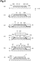
- FIG. 5 is a diagram (cross-sectional view) illustrating a method of manufacturing an organic EL element (organic electronic element) according to a modified example of the first embodiment.
- the method of manufacturing an organic EL element of the modified example differs from the method of manufacturing an organic EL element of the first embodiment in that it includes a mask forming step illustrated in FIG. 5(b) to FIG. 5(d) in place of the mask forming step illustrated in FIG. 1(b) to FIG. 1(e) in the first embodiment.
- the first electrode forming step and the functional layer forming step illustrated in FIG. 5(a) are the same as the first electrode forming step and the functional layer forming step illustrated in FIG.
- the second electrode forming step illustrated in FIG. 5(e) is the same as the second electrode forming step illustrated in FIG. 1(f) .
- the mask separating step illustrated in FIG. 5(f) is the same as the mask separating step illustrated in FIG. 1(g) .
- the removable release sheet 32A and the mask film 31 having flexibility are sequentially laminated on the substrate 10 such that the positive electrode layer 21 and the light emitting layer 23 or the functional layer are covered.
- the release sheet 32A and the mask film 31 are processed into the mask element 30. Specifically, an opening region is cut out from the release sheet 32A and the mask film 31 such that the mask element 30 covers the edge portions 21a and 23a in the positive electrode layer 21 and the light emitting layer 23 or the functional layer, and the mask element 30 surrounds the edge portion 23b in the light emitting layer 23 or the functional layer, and thus the mask element 30 is produced.
- FIG. 6 is a diagram (cross-sectional view) illustrating a method of manufacturing an organic EL element (organic electronic element) according to the second embodiment.
- the method of manufacturing an organic EL element of the second embodiment differs from the method of manufacturing an organic EL element of the first embodiment in that the order of the functional layer forming step and the mask forming step in the first embodiment is changed.
- the positive electrode layer 21 for the organic EL portion 20 is pattern-formed on the film-like substrate 10.
- the lead-out electrode layer 22A to be bonded to the negative electrode layer may be pattern-formed on the film-like substrate 10 (first electrode forming step).
- the mask element with an opening 30 is formed on the substrate 10 to surround four sides of the positive electrode layer 21 in an opening region.
- the mask element with an opening 30 is a grid-like mask element that crosses the substrate 10 in the longitudinal direction X and the width direction Y.
- the mask element 30 is formed to cover the edge portion 21a in the positive electrode layer 21.
- the first removable release sheet 32A, the mask film 31 having flexibility, the second removable release sheet 32B, and the carrier film 33 are laminated in that order, and the release sheet 32A and the mask film 31 are processed into the mask element 30 to produce the lamination film 34.
- the opening region is cut out from the release sheet 32A and the mask film 31 and thus the mask element 30 is produced.
- the lamination film 34 is laminated on the substrate 10 such that the mask element 30 covers the edge portion 21a of the positive electrode layer 21 and the mask element 30 covers the edge portion 22b of the negative electrode layer 22.
- the removable release sheet 32B and the carrier film 33 in the lamination film 34 are separated from the mask element 30 (mask forming step).
- the light emitting layer 23 or the functional layer for the organic EL portion 20 is pattern-formed on the positive electrode layer 21 and the lead-out electrode layer 22A.
- the edge portion 23a of the light emitting layer 23 or the functional layer is formed such that it comes in contact with the mask element 30 and is formed to be shorter than the edge portion 21a such that the edge portion 21a of the positive electrode layer 21 is exposed to obtain a lead-out wiring connecting portion.
- the edge portion 23b of the light emitting layer 23 or the functional layer is formed such that it provides a space with the mask element 30 therebetween and is formed to be shorter than the edge portion 22b such that the edge portion 22b of the negative electrode layer 22 is exposed to obtain a lead-out wiring connecting portion.
- the edge portion 23c of the light emitting layer 23 is formed to be longer than the edge portion 21c such that the edge portion 21c of the positive electrode layer 21 is covered and the edge portion 23d of the light emitting layer 23 is formed to be longer than the edge portion 21d such that the edge portion 21d of the positive electrode layer 21 is covered (functional layer forming step).
- the negative electrode layer 22 for the organic EL portion 20 is formed on the light emitting layer 23.
- the mask element 30 is used as a mask (second electrode forming step).
- the mask element 30 is separated from the substrate 10 (mask separating step).
- the mask element 30 may be separated therefrom.
- FIG. 7 shows diagrams (cross-sectional views) illustrating a method of manufacturing an organic EL element (organic electronic element) according to a modified example of the second embodiment.
- the method of manufacturing an organic EL element of the modified example differs from the method of manufacturing an organic EL element of the second embodiment in that it includes a mask forming step illustrated FIG. 7(b) to FIG. 7(d) in place of the mask forming step illustrated in FIG. 6(b) to FIG. 6(e) in the second embodiment.
- the first electrode forming step illustrated in FIG. 7(a) is the same as the first electrode forming step illustrated in FIG. 6(a) , the functional layer forming step and the second electrode forming step illustrated in FIG.
- FIG. 7(e) are the same as the functional layer forming step and the second electrode forming step illustrated in FIG. 6(f)
- the mask separating step illustrated in FIG. 7(f) is the same as the mask separating step illustrated in FIG. 6(g) .
- FIG. 7(b) A mask forming step illustrated in FIG. 7(b) to FIG. 7(d) will be described below.
- the removable release sheet 32A and the mask film 31 having flexibility are sequentially laminated on the substrate 10 such that the positive electrode layer 21 is covered.
- the release sheet 32A and the mask film 31 are processed into the mask element 30. Specifically, an opening region is cut out from the release sheet 32A and the mask film 31 such that the mask element 30 covers the edge portion 21a of the positive electrode layer 21, the mask element 30 covers the edge portion 22b of the negative electrode layer 22, and the mask element 30 surrounds the edge portions 21c and 21d of the positive electrode layer 21, and thus the mask element 30 is produced.
- the present invention is not limited to the above embodiments and various modifications can be made.
- an organic EL element including a light emitting layer (functional layer) between a pair of electrodes has been exemplified in the present embodiment, features of the present invention can also be applied to various organic EL elements illustrated below.
- the symbol "/" indicates that layers between which the symbol “/" is interposed are laminated adjacent to each other.
- the method of manufacturing an organic EL element in the form in which a positive electrode layer is disposed on the side of the substrate with respect to the light emitting layer and a negative electrode layer is disposed on the side opposite to the substrate with respect to the light emitting layer has been exemplified in the present embodiment.
- the present invention can also be applied to a manufacturing method in the form in which the negative electrode layer is disposed on the side of the substrate with respect to the light emitting layer and the positive electrode layer is disposed on the side opposite to the substrate with respect to the light emitting layer.
- an organic EL element organic electronic element
- the features of the present invention can also be applied to a method of manufacturing an organic solar cell (organic electronic element) and an organic transistor (organic electronic element).
Landscapes
- Engineering & Computer Science (AREA)
- Manufacturing & Machinery (AREA)
- Physics & Mathematics (AREA)
- Optics & Photonics (AREA)
- Electroluminescent Light Sources (AREA)
Abstract
Description
- The present invention relates to a method of manufacturing an organic electronic element having flexibility such as an organic EL element, an organic solar cell, and an organic transistor, and an organic electronic element having flexibility.
- Organic electronic elements such as an organic electro luminescence (EL) element, an organic solar cell, and an organic transistor are known. This type of organic electronic element includes various functional layers such as a light emitting layer, a hole injection layer, a hole transport layer, an electron transport layer, an electron injection layer, an active layer, a semiconductor layer, and an insulating layer which contain an organic material.
- This type of organic electronic element may be formed on a film-like substrate (substrate having flexibility, flexible substrate) to form a film shape. As a method of manufacturing a film-like organic electronic element, a method of forming various layers using a roll-to-roll process is known. In
Patent Literature 1, an organic EL element manufacturing method is disclosed as a method of manufacturing this type of organic electronic element. - In the organic EL element manufacturing method disclosed in
Patent Literature 1, when the film-like substrate is wound after a step of forming various layers, a flexible polymer film with a predetermined width is applied to and wound as a winding auxiliary member around both ends in the width direction. Thus, during winding, it is possible to prevent a film surface of the organic EL element from rubbing against the substrate and a film surface of the organic EL element from being scratched. - In addition, in the method of manufacturing this type of organic electronic element, as a method of forming an electrode, a vapor deposition method, a sputtering method, and a CVD method are generally used. In the method of forming this type of electrode, a shadow mask is disposed in a vapor deposition device, a sputtering device, or a CVD device, and a film-like substrate and the mask are aligned to form a film.
- [Patent Literature 1] Japanese Patent Application Laid-Open Publication No.
2006-294536 - Incidentally, in the organic EL element manufacturing method disclosed in
Patent Literature 1, when the width of the film-like substrate becomes wider, it may not be possible to prevent a film surface (surface on which an organic layer is formed) on which the organic EL element of the film-like substrate is formed and a back surface of the substrate from coming in contact with each other in the central portion in the width direction due to sagging. Further, it may not be possible to prevent a film surface (surface on which an organic layer is formed) and a roller in a manufacturing device using a roll-to-roll process from coming in contact with each other in the central portion in the width direction. When this type of contact occurs, the organic EL layer may be damaged. A film transport mechanism may be complicated in order to avoid such damage and the productivity may decrease. - In addition, in a continuous step using a roll-to-roll process, in an electrode forming step (in particular, a second electrode forming step), the continuous productivity may decrease due to setting of an electrode forming mask and the substrate.
- Therefore, an object of an aspect of the present invention is to provide a method of manufacturing an organic electronic element through which it is possible to achieve both protection of a film surface and improvement in continuous productivity in an organic electronic element manufacturing method using a roll-to-roll process and an organic electronic element.
- An organic electronic element manufacturing method according to an aspect of the present invention is a method of manufacturing an organic electronic element having flexibility using a roll-to-roll process. The method includes a first electrode forming step in which a first electrode is pattern-formed onto a flexible substrate; a functional layer forming step in which a functional layer containing an organic material is pattern-formed onto the first electrode; and a mask forming step in which a mask element having flexibility is formed on the substrate such that it has an opening on at least a portion of the functional layer and at least a portion of the first electrode with the functional layer therebetween and covers edge portions on at least one side of the first electrode and the functional layer.
- According to the method of manufacturing an organic electronic element according to the aspect of the present invention, when the substrate is first wound on a roller after the first electrode and the functional layer are formed, the mask element having flexibility can prevent a film surface of the functional layer from coming in contact with a back surface of the substrate and additionally prevent a film surface of the functional layer from coming in direct contact with the roller. As a result, it is possible to prevent the film surface of the functional layer from being physically or chemically damaged (protection of the film surface).
- In addition, according to the method of manufacturing an organic electronic element according to the aspect of the present invention, the mask element can be used as a mask for forming a second electrode, and it is not necessary to set a shadow mask for forming the second electrode as in the related art. Therefore, it is possible to improve continuous productivity (improvement in continuous productivity).
- Here, since the mask element covers edge portions on at least one side of the first electrode and the functional layer, when the mask element is used as a mask for forming the second electrode, it is possible to prevent the first electrode and the second electrode from coming in contact with each other and it is possible to form a connecting portion for lead-out wiring on the edge portion on at least one side of the first electrode.
- In the mask forming step, the mask element having flexibility may be formed on the substrate to surround four sides of the first electrode and the functional layer in an opening region.
- Accordingly, when a plurality of organic electronic elements are two-dimensionally arranged on the substrate, it is possible to form a grid-like mask element that crosses an elongated substrate in the longitudinal direction and the width direction. Therefore, when the substrate is first wound on a roller after the first electrode and the functional layer are formed, even if the width of the elongated substrate becomes wider, the grid-like mask element can prevent the occurrence of sagging and it is possible to prevent a film surface of the functional layer from coming in contact with a back surface of the substrate also in the central portion in the width direction. In addition, it is possible to prevent a film surface of the functional layer from coming in direct contact with a roller. As a result, it is possible to prevent a film surface of the functional layer from being physically or chemically damaged (protection of the film surface).
- In addition, the mask forming step may include a step in which a lamination film in which a first removable release sheet, a mask film having flexibility, a second removable release sheet, and a carrier film are laminated in that order, and the first removable release sheet and the mask film are processed into the mask element having the opening is produced; a step in which the lamination film is laminated on the substrate such that the mask element covers edge portions on at least one side of the first electrode and the functional layer; and a step in which the second removable release sheet and the carrier film in the lamination film are separated from the mask element.
- For example, when an opening is formed in the mask film, if there is no carrier film, since tension is applied to the mask film in the longitudinal direction in roll-to-roll, the mask film becomes bent. However, accordingly, since the carrier film is backed, the tension is dispersed in the carrier film and additionally the carrier film is also present in an opening portion of the mask film. Thus, yawing of the mask film due to the opening is significantly reduced. In addition, since processing into the mask element is performed before the lamination film is laminated on the substrate, the substrate is not damaged by processing into the mask element. In addition, direct contact of the first electrode or the functional layer with the mask element, the carrier film, and the release sheet is prevented according to the opening processed into the mask element. Therefore, it is possible to prevent the occurrence of defects caused by adherence of contamination components, rubbing, and pushing and indentation of foreign substances due to contact.
- In addition, the mask forming step may include a step in which a removable release sheet and a mask film having flexibility are laminated on the substrate such that the first electrode and the functional layer are covered; and a step in which the removable release sheet and the mask film are processed into the mask element having the opening. Specifically, the mask element is directly laminated on a light emitting region including a first electrode and a functional layer, and is cut into an arbitrary shape that forms a second electrode including the light emitting region, and this portion is separated therefrom and removed.
- Accordingly, since a carrier film is not used, economic efficiency is excellent, and the mask element is laminated on the light emitting region. Therefore, when the mask element is processed and the substrate is transported, it is possible to prevent foreign substances from adhering to the light emitting region. In addition, when separation and removal are performed, foreign substances that are adhered before lamination can be removed all at once and a failure rate of a device can be reduced.
- In addition, the method of manufacturing an organic electronic element may further include a second electrode forming step in which a second electrode is formed on the functional layer using the mask element.
- In addition, the method of manufacturing an organic electronic element may further include a sealing film forming step in which a sealing film is formed on the second electrode using the mask element. Accordingly, the mask element can be used as a mask for forming a sealing film and it is not necessary to set a shadow mask for forming the sealing film as in the related art. Therefore, it is possible to improve continuous productivity.
- In addition, the method of manufacturing an organic electronic element may further include a mask separating step in which the mask element is separated from the substrate.
- A method of manufacturing an organic electronic element according to another aspect of the present invention is a method of manufacturing an organic electronic element having flexibility using a roll-to-roll process. The method includes a first electrode forming step in which a first electrode is pattern-formed onto a flexible substrate; and a mask forming step in which a mask element having flexibility is formed on the substrate such that it has an opening on at least a portion of the first electrode and covers an edge portion on at least one side of the first electrode. In the method of manufacturing an organic electronic element according to another aspect, after the mask forming step, a functional layer forming step in which a functional layer containing an organic material is pattern-formed on the first electrode is performed.
- Also in the method of manufacturing an organic electronic element according to another aspect of the present invention, when the substrate is first wound on a roller after the first electrode and the functional layer are formed, the mask element having flexibility can prevent a film surface of the functional layer from coming in contact with a back surface of the substrate and additionally prevent a film surface of the functional layer from coming in direct contact with the roller. As a result, it is possible to prevent the film surface of the functional layer from being physically or chemically damaged (protection of the film surface).
- In addition, also in the method of manufacturing an organic electronic element according to another aspect of the present invention, the mask element can be used as a mask for forming a second electrode, and it is not necessary to set a shadow mask for forming the second electrode as in the related art. Therefore, it is possible to improve continuous productivity (improvement in continuous productivity).
- Here, since the mask element covers an edge portion on at least one side of the first electrode, when the mask element is used as a mask for forming a second electrode, it is possible to prevent the first electrode and the second electrode from coming in contact with each other and it is possible to form a connecting portion for lead-out wiring on the edge portion on at least one side of the first electrode.
- In the mask forming step, the mask element having flexibility may be formed on the substrate to surround four sides of the first electrode in an opening region.
- Accordingly, when a plurality of organic electronic elements are two-dimensionally arranged on the substrate, it is possible to form a grid-like mask element that intersects the longitudinal direction and the width direction of an elongated substrate. Therefore, when the substrate is first wound on a roller after the first electrode and the functional layer are formed, even if the width of the elongated substrate becomes wider, the grid-like mask element can prevent the occurrence of sagging and it is possible to prevent a film surface of the functional layer from coming in contact with a back surface of the substrate also in the central portion in the width direction. In addition, it is possible to prevent a film surface of the functional layer from coming in direct contact with a roller. As a result, it is possible to prevent a film surface of the functional layer from being physically or chemically damaged (protection of the film surface).
- In addition, the mask forming step may include a step in which a lamination film in which a first removable release sheet, a mask film having flexibility, a second removable release sheet, and a carrier film are laminated in that order, and the first removable release sheet and the mask film are processed into the mask element having the opening is produced, a step in which the lamination film is laminated on the substrate such that the mask element covers an edge portion on at least one side of the first electrode; and a step in which the second removable release sheet and the carrier film in the lamination film are separated from the mask element.
- Accordingly, similarly to the above, since the carrier film is backed, the tension is dispersed in the carrier film and additionally the carrier film is also present in an opening portion of the mask film. Thus, yawing of the mask film due to the opening is significantly reduced. In addition, since processing into the mask element is performed before the lamination film is laminated on the substrate, the substrate is not damaged by processing into the mask element. In addition, direct contact of the first electrode with the mask element, the carrier film, and the release sheet is prevented according to the opening processed into the mask element. Therefore, it is possible to prevent the occurrence of defects caused by adherence of contamination components, rubbing, and pushing and indentation of foreign substances due to contact.
- In addition, the mask forming step may include a step in which a removable release sheet and a mask film having flexibility are laminated in that order on the substrate such that the first electrode is covered; and a step in which the removable release sheet and the mask film are processed into the mask element having the opening. Specifically, the mask element is directly laminated on a light emitting region in the first electrode and is cut into an arbitrary shape that forms a second electrode including the light emitting region, and this portion is separated therefrom and removed.
- Accordingly, similarly to the above, since the carrier film is not used, economic efficiency is excellent, and the mask element is laminated on the light emitting region. Therefore, when the mask element is processed and the substrate is transported, it is possible to prevent foreign substances from adhering to the light emitting region. In addition, when separation and removal are performed, foreign substances that are adhered before lamination can be removed all at once and a failure rate of a device can be reduced.
- In addition, the method of manufacturing an organic electronic element according to another aspect may further include a functional layer forming step in which a functional layer containing an organic material is pattern-formed onto the first electrode after the mask forming step; and a second electrode forming step in which a second electrode is formed on the functional layer using the mask element.
- In addition, the method of manufacturing an organic electronic element according to another aspect may further include a sealing film forming step in which a sealing film is formed on the second electrode using the mask element. Accordingly, the mask element can be used as a mask for forming a sealing film and it is not necessary to set a shadow mask for forming the sealing film as in the related art. Therefore, it is possible to improve continuous productivity.
- In addition, the method of manufacturing an organic electronic element according to another aspect may further include a mask separating step in which the mask element is separated from the substrate.
- An organic electronic element according to an aspect of the present invention can be manufactured by the method of manufacturing an organic electronic element or a method of manufacturing an organic electronic element according to another aspect.
- According to an aspect of the present invention, in an organic electronic element manufacturing method using a roll-to-roll process, it is possible to achieve both protection of a film surface and improvement in continuous productivity.
-
-
FIG. 1(a), FIG. 1(b), FIG. 1(c), FIG. 1(d), FIG. 1(e), FIG. 1(f) and FIG. 1(g) are diagrams (cross-sectional views) illustrating a method of manufacturing an organic EL element (organic electronic element) according to a first embodiment. -
FIG. 2 is a illustrating an intermediate product for the organic EL element after a mask forming step illustrated inFIG. 1(e) when viewed from above. -
FIG. 3 is a diagram illustrating an elongated substrate (roll substrate) in which a plurality of intermediate products for the organic EL element after the mask forming step illustrated inFIG. 1(e) are two-dimensionally arranged when viewed from above. -
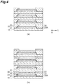
FIG. 4(a) is a diagram illustrating an intermediate product for the organic EL element after the mask forming step illustrated inFIG. 1(e) andFIG. 4(b) is a diagram (cross-sectional view) illustrating a state in which the intermediate product for the organic EL element after a second electrode forming step illustrated inFIG. 1(f) is wound into a roll shape. -
FIG. 5(a), FIG. 5(b), FIG. 5(c), FIG. 5(d), FIG. 5(e) and FIG. 5(f) are diagrams (cross-sectional views) illustrating a method of manufacturing an organic EL element (organic electronic element) according to a modified example of the first embodiment. -
FIG. 6(a), FIG. 6(b), FIG. 6(c), FIG. 6(d), FIG. 6(e), FIG. 6(f) and FIG. 6(g) are diagrams (cross-sectional views) illustrating a method of manufacturing an organic EL element (organic electronic element) according to a second embodiment. -
FIG. 7(a), FIG. 7(b), FIG. 7(c), FIG. 7(d), FIG. 7(e) and FIG. 7(f) are diagrams (cross-sectional views) illustrating a method of manufacturing an organic EL element (organic electronic element) according to a modified example of the second embodiment. -
FIG. 8 is a diagram illustrating the intermediate product corresponding toFIG. 2 , which is an intermediate product for the organic EL element according to the modified example, when viewed from above. -
FIG. 9 is a diagram illustrating the intermediate product corresponding toFIG. 2 , which is an intermediate product for the organic EL element according to the modified example, when viewed from above. - Embodiments will be described below in detail with reference to the drawings. Here, the same or corresponding components in the drawings are denoted with the same reference numerals.
- [First embodiment]
FIG. 1 shows diagrams (cross-sectional views) illustrating a method of manufacturing an organic EL element (organic electronic element) according to a first embodiment.FIG. 2 is a diagram illustrating the organic EL element illustrated inFIG. 1(e) when viewed from above. In addition,FIG. 3 is a diagram illustrating an elongated substrate (roll substrate) in which a plurality of organic EL elements illustrated inFIG. 1(e) are two-dimensionally arranged when viewed from above. In anorganic EL element 1 in this example, asubstrate 10 is set as a light emitting surface. - First, using a continuous transport method such as a roll-to-roll process, according to a vapor deposition method, a sputtering method, an ion plating method, a plating method, a transfer method, or the like, as illustrated in
FIG. 1(a) ,FIG. 2 , andFIG. 3 , on the film-like substrate (substrate having flexibility, flexible substrate) 10, a positive electrode layer (first electrode layer) 21 for anorganic EL portion 20 is pattern-formed. In addition, on the film-like substrate 10, a lead-outelectrode layer 22A to be bonded to a negative electrode layer (second electrode layer) to be described below may be pattern-formed. Here, thepositive electrode layer 21 and the lead-outelectrode layer 22A may be electrically insulated, may be spatially separated in a longitudinal direction X of thesubstrate 10, or may be isolated with an insulating layer therebetween (first electrode forming step). A width direction of thesubstrate 10 will be set below as Y - For the film-
like substrate 10, a material having optical transparency such as PEN (polyethylene naphthalate) and PET (polyethylene terephthalate) may be used. For thepositive electrode layer 21 and the lead-outelectrode layer 22A, in particular, for a light emitting area of thepositive electrode layer 21, for example, an electrode exhibiting optical transparency, more specifically, a conductive metal oxide thin film made of a relatively transparent material such as ITO (Indium Tin Oxide) and IZO (Indium Zinc Oxide) may be used. In addition, for the light emitting area of thepositive electrode layer 21, a mesh electrode in which a metal is formed into a mesh shape can be used. A region other than the light emitting area of thepositive electrode layer 21 and the lead-outelectrode layer 22A may be made of the same material as the light emitting area of thepositive electrode layer 21, or made of different materials, or may be opaque. - Next, using a roll-to-roll process, according to a coating method (for example, an ink jet printing method, a slit coating method, a spray method, or a screen printing method), a
light emitting layer 23 for theorganic EL portion 20 is pattern-formed on thepositive electrode layer 21 or on thepositive electrode layer 21 and the lead-outelectrode layer 22A. Here, between the light emittinglayer 23 and thepositive electrode layer 21, functional layers such as a hole injection layer, a hole transport layer, and an electron blocking layer may be provided. In addition, between the light emittinglayer 23 and thenegative electrode layer 22 to be described below, functional layers such as an electron injection layer, an electron transport layer, and a hole blocking layer may be provided. In addition, between thepositive electrode layer 21 and thenegative electrode layer 22, an insulating layer having a higher electrical resistance than an electrical resistance in a lamination direction of a region in which the light emitting layer of the light emitting region and the functional layer are laminated may be provided in a region other than the light emitting region. - An
edge portion 23a on one side in the longitudinal direction X of thelight emitting layer 23 or the functional layer is formed to be shorter than anedge portion 21a such that theedge portion 21a on one side in the longitudinal direction X of thepositive electrode layer 21 is exposed to obtain a lead-out wiring connecting portion. Anedge portion 23b on the other side in the longitudinal direction X of thelight emitting layer 23 or the functional layer is formed to be shorter than anedge portion 22b such that theedge portion 22b on the other side in the longitudinal direction X of the lead-outelectrode layer 22A is exposed to obtain a lead-out wiring connecting portion. On the other hand, anedge portion 23c on one side in the width direction Y of thelight emitting layer 23 or the functional layer is formed to be longer than anedge portion 21c such that theedge portion 21c on one side in the width direction Y of thepositive electrode layer 21 is covered. Theedge portion 23d on the other side in the width direction Y of thelight emitting layer 23 is formed to be longer than anedge portion 21d such that theedge portion 21d on the other side in the width direction Y of thepositive electrode layer 21 is covered. Here, thelight emitting layer 23 may be deposited between thepositive electrode layer 21 and the lead-outelectrode layer 22A (functional layer forming step). - Here, as illustrated in
FIG. 8 , thelight emitting layer 23 or the functional layer may be formed such that at least aportion 21A of thepositive electrode layer 21 on the side of theedge portion 21a on one side in the longitudinal direction X of thepositive electrode layer 21 is exposed to obtain a lead-out wiring connecting portion and at least theportion 21A on the side of theedge portion 21a of thepositive electrode layer 21 is exposed. In addition, thelight emitting layer 23 or the functional layer may be formed such that at least aportion 22B of the lead-outelectrode layer 22A on the side of theedge portion 22b on the other side in the longitudinal direction X of the lead-outelectrode layer 22A is exposed to obtain a lead-out wiring connecting portion and at least a portion on the side of theedge portion 22b of the lead-outelectrode layer 22A is exposed. - The
light emitting layer 23 contains various known organic EL materials such as low-molecular-weight type and high-molecular-weight type materials. - Next, using a roll-to-roll process, as illustrated in
FIG. 1(b) to FIG. 1(e) ,FIG. 2 andFIG. 3 , a mask element with anopening 30 is formed on thesubstrate 10 to surround four sides of thepositive electrode layer 21 and thelight emitting layer 23 or the functional layer in an opening region. In other words, the mask element with anopening 30 is a grid-like mask element that crosses thesubstrate 10 in the longitudinal direction X and the width direction Y. Themask element 30 is formed to cover theedge portions positive electrode layer 21 and thelight emitting layer 23 or the functional layer. In addition, themask element 30 is formed to surround theedge portion 23b in thelight emitting layer 23 or the functional layer. - In addition, the opening of the
mask element 30 may have an arbitrary shape, for example, a circular shape or an elliptical shape as illustrated inFIG. 8 . When the opening having an arbitrary shape is used, since thenegative electrode layer 22 to be described below is formed into the shape of the opening, it is possible to obtain an arbitrary shape according to the shape of the opening, that is, it is possible to obtain a light emitting region having an arbitrary light emission pattern. - In addition, as illustrated in
FIG. 8 , on the side of the lead-outelectrode layer 22A, themask element 30 may be formed such that the opening overlaps the portion (lead-out wiring connecting portion) 22B from which the lead-outelectrode layer 22A is exposed, and thus the lead-outelectrode layer 22A and thenegative electrode layer 22 can be electrically connected. In addition, as illustrated inFIG. 8 , on the side of theedge portion 21a of thepositive electrode layer 21, themask element 30 may be formed such that the opening does not overlap the portion (lead-out wiring connecting portion) 21A from which thepositive electrode layer 21 is exposed. - In addition, as illustrated in
FIG. 9 , the lead-outelectrode layer 22A of thenegative electrode layer 22 may be omitted. In addition, as illustrated inFIG. 1 ,FIG. 8 andFIG. 9 , the opening of themask element 30 may not overlap an exposed portion of thepositive electrode layer 21 or the opening of themask element 30 may overlap an exposed portion of thepositive electrode layer 21. In this case, an insulating layer may be provided between thepositive electrode layer 21 and thenegative electrode layer 22. - In this manner, the
mask element 30 may be formed on thesubstrate 10 such that it has an opening on at least a portion of thelight emitting layer 23 or the functional layer and on at least a portion of thepositive electrode layer 21 with thelight emitting layer 23 or the functional layer therebetween and covers theedge portions positive electrode layer 21 and thelight emitting layer 23 or the functional layer. - Specifically, first, as illustrated in
FIG. 1(b) and FIG. 1(c) , a firstremovable release sheet 32A, amask film 31 having flexibility, a secondremovable release sheet 32B, and acarrier film 33 are laminated in that order and therelease sheet 32A and themask film 31 are processed into themask element 30 to produce alamination film 34. Specifically, the opening region is cut out from therelease sheet 32A and themask film 31 and thus themask element 30 is produced. - Next, as illustrated in
FIG. 1(d) , thelamination film 34 is laminated on thesubstrate 10 such that themask element 30 covers theedge portions positive electrode layer 21 and thelight emitting layer 23 or the functional layer and themask element 30 surrounds theedge portion 23b in thelight emitting layer 23 or the functional layer. - Next, as illustrated in
FIG. 1(e) , theremovable release sheet 32B and thecarrier film 33 in thelamination film 34 are separated from the mask element 30 (mask forming step). - As a material of the
mask film 31, that is, a material of themask element 30, a material having the same coefficient of linear thermal expansion as the substrate can be selected in order to prevent the occurrence of separation and wrinkles depending on a temperature during a second electrode forming process. Specifically, examples of a material of themask element 30 include PEN and PET. In addition, for themask element 30, a plastic film having a glass transition temperature that is higher than the temperature during the second electrode forming process can be used. Specifically, examples of a material of themask element 30 include a polyimide and a fluorine resin. In addition, for themask element 30, a metal foil, a composite member in which a metal, particularly, Al or Cu, and a plastic film are laminated or a glass cloth can be used. For theremovable release sheets carrier film 33 include PET, PC (polycarbonate), PS (polystyrene), and PE (polyethylene). - Next, using a roll-to-roll process, according to a vapor deposition method, a sputtering method, an ion plating method, a plating method, a transfer method, or the like, as illustrated in
FIG. 1(f) , thenegative electrode layer 22 for theorganic EL portion 20 is formed on thelight emitting layer 23 or the functional layer. In this case, themask element 30 is used as a mask (second electrode forming step). As thenegative electrode layer 22, for example, an electrode exhibiting light reflectivity, more specifically, a conductive metal thin film made of a metal material may be used. In particular, in consideration of light reflectivity and conductivity, as thenegative electrode layer 22, Al, an Al alloy (such as AlNd), Ag, and an Ag alloy (such as AgPaCu) are preferable. - Next, using a roll-to-roll process, as illustrated in
FIG. 1(g) , themask element 30 is separated from the substrate 10 (mask separating step). Here, after a sealing film is formed on thenegative electrode layer 22 using the mask element 30 (sealing film forming step), themask element 30 may be separated therefrom. As a material of the sealing film, a silicon oxide, a silicon oxynitride and a silicon nitride (may contain carbon in a composition) such as SiOx, SiOxNy, and SiNx, and an aluminum oxide such as AlxOy may be used for an inorganic film having a moisture permeability barrier property. Examples of a method of forming a sealing film include a CVD method, a sputtering method, a vapor deposition method, and a method of forming a film by coating a precursor and applying light or heat energy. In addition, in order to perform flattening or to prevent penetration of pinholes into the inorganic film, an organic layer made of an acrylic resin or the like may be formed. In addition, the organic layer may contain a metal oxide, a metal complex, or a getter material having a moisture capture function such as a zeolite. - According to the method of manufacturing an organic EL element of the first embodiment, when the
substrate 10 is first wound on a roller after thepositive electrode layer 21 and thelight emitting layer 23 or the functional layer are formed (refer to a roll cross section illustrated inFIG. 4(a) ), themask element 30 having flexibility makes it possible to prevent the film surface of thelight emitting layer 23 or the functional layer from coming in contact with the back surface of thesubstrate 10 and additionally, it is possible to prevent the film surface of thelight emitting layer 23 or the functional layer from coming in direct contact with a roller. In particular, even if the width of thesubstrate 10 becomes larger, the grid-like mask element 30 makes it possible to prevent the occurrence of sagging, and it is possible to prevent the film surface of thelight emitting layer 23 or the functional layer from coming in contact with the back surface of thesubstrate 10 also in the central portion in the width direction Y. As a result, it is possible to prevent a film surface of thelight emitting layer 23 or the functional layer from being physically or chemically damaged (protection of the film surface). - Similarly, even when the
substrate 10 is first wound on a roller after thenegative electrode layer 22 is formed (refer to a roll cross section illustrated inFIG. 4(b) ), themask element 30 having flexibility makes it possible to prevent the film surface of thenegative electrode layer 22 from coming in contact with the back surface of thesubstrate 10, and additionally, it is possible to prevent the film surface of thenegative electrode layer 22 from coming in direct contact with a roller. In particular, even if the width of thesubstrate 10 becomes larger, the grid-like mask element 30 makes it possible to prevent the occurrence of sagging, and it is possible to prevent the film surface of thenegative electrode layer 22 from coming in contact with the back surface of thesubstrate 10 also in the central portion in the width direction Y. As a result, it is possible to prevent the film surface of thenegative electrode layer 22 from being physically or chemically damaged. - In addition, according to method of manufacturing an organic EL element of the first embodiment, the
mask element 30 can be used as a mask for forming thenegative electrode layer 22, and it is not necessary to set a shadow mask for forming thenegative electrode layer 22 as in the related art. Therefore, it is possible to improve continuous productivity (improvement in continuous productivity). - Here, since the
mask element 30 covers theedge portions positive electrode layer 21 and thelight emitting layer 23 or the functional layer, when themask element 30 is used as a mask for forming thenegative electrode layer 22, it is possible to prevent thepositive electrode layer 21 and thenegative electrode layer 22 from coming in contact with each other and it is possible to form a connecting portion for lead-out wiring on theedge portion 21a of thepositive electrode layer 21. In addition, since themask element 30 covers theedge portion 22b in a portion of thenegative electrode layer 22, it is possible to form a connecting portion for lead-out wiring on theedge portion 22b of thenegative electrode layer 22. - [Modified example of first embodiment]
FIG. 5 is a diagram (cross-sectional view) illustrating a method of manufacturing an organic EL element (organic electronic element) according to a modified example of the first embodiment. The method of manufacturing an organic EL element of the modified example differs from the method of manufacturing an organic EL element of the first embodiment in that it includes a mask forming step illustrated inFIG. 5(b) to FIG. 5(d) in place of the mask forming step illustrated inFIG. 1(b) to FIG. 1(e) in the first embodiment. Here, the first electrode forming step and the functional layer forming step illustrated inFIG. 5(a) are the same as the first electrode forming step and the functional layer forming step illustrated inFIG. 1(a) , and the second electrode forming step illustrated inFIG. 5(e) is the same as the second electrode forming step illustrated inFIG. 1(f) . The mask separating step illustrated inFIG. 5(f) is the same as the mask separating step illustrated inFIG. 1(g) . - The mask forming step illustrated in
FIG. 5(b) to FIG. 5(d) will be described below. First, as illustrated inFIG. 5(b) , theremovable release sheet 32A and themask film 31 having flexibility are sequentially laminated on thesubstrate 10 such that thepositive electrode layer 21 and thelight emitting layer 23 or the functional layer are covered. - Next, as illustrated in
FIG. 5(c) and FIG. 5(d) , therelease sheet 32A and themask film 31 are processed into themask element 30. Specifically, an opening region is cut out from therelease sheet 32A and themask film 31 such that themask element 30 covers theedge portions positive electrode layer 21 and thelight emitting layer 23 or the functional layer, and themask element 30 surrounds theedge portion 23b in thelight emitting layer 23 or the functional layer, and thus themask element 30 is produced. - Also in the method of manufacturing an organic EL element of the modified example, it is possible to obtain the same advantages as in the method of manufacturing an organic EL element of the first embodiment.
- [Second embodiment]
FIG. 6 is a diagram (cross-sectional view) illustrating a method of manufacturing an organic EL element (organic electronic element) according to the second embodiment. The method of manufacturing an organic EL element of the second embodiment differs from the method of manufacturing an organic EL element of the first embodiment in that the order of the functional layer forming step and the mask forming step in the first embodiment is changed. - First, using a continuous transport method such as a roll-to-roll process, according to a vapor deposition method, a sputtering method, an ion plating method, a plating method, a transfer method or the like, as illustrated in
FIG. 6(a) , thepositive electrode layer 21 for theorganic EL portion 20 is pattern-formed on the film-like substrate 10. In addition, the lead-outelectrode layer 22A to be bonded to the negative electrode layer (second electrode layer) may be pattern-formed on the film-like substrate 10 (first electrode forming step). - Next, using a roll-to-roll process, as illustrated in
FIG. 6(b) to FIG. 6(e) , the mask element with anopening 30 is formed on thesubstrate 10 to surround four sides of thepositive electrode layer 21 in an opening region. In other words, the mask element with anopening 30 is a grid-like mask element that crosses thesubstrate 10 in the longitudinal direction X and the width direction Y. Themask element 30 is formed to cover theedge portion 21a in thepositive electrode layer 21. - Specifically, first, as illustrated in
FIG. 6(b) and FIG. 6(c) , the firstremovable release sheet 32A, themask film 31 having flexibility, the secondremovable release sheet 32B, and thecarrier film 33 are laminated in that order, and therelease sheet 32A and themask film 31 are processed into themask element 30 to produce thelamination film 34. Specifically, the opening region is cut out from therelease sheet 32A and themask film 31 and thus themask element 30 is produced. - Next, as illustrated in
FIG. 6(d) , thelamination film 34 is laminated on thesubstrate 10 such that themask element 30 covers theedge portion 21a of thepositive electrode layer 21 and themask element 30 covers theedge portion 22b of thenegative electrode layer 22. - Next, as illustrated in
FIG. 6(e) , theremovable release sheet 32B and thecarrier film 33 in thelamination film 34 are separated from the mask element 30 (mask forming step). - Next, using a roll-to-roll process, according to a coating method (for example, an ink jet printing method, a slit coating method, a spray method, or a screen printing method), as illustrated in
FIG. 6(f) , thelight emitting layer 23 or the functional layer for theorganic EL portion 20 is pattern-formed on thepositive electrode layer 21 and the lead-outelectrode layer 22A. Theedge portion 23a of thelight emitting layer 23 or the functional layer is formed such that it comes in contact with themask element 30 and is formed to be shorter than theedge portion 21a such that theedge portion 21a of thepositive electrode layer 21 is exposed to obtain a lead-out wiring connecting portion. On the other hand, theedge portion 23b of thelight emitting layer 23 or the functional layer is formed such that it provides a space with themask element 30 therebetween and is formed to be shorter than theedge portion 22b such that theedge portion 22b of thenegative electrode layer 22 is exposed to obtain a lead-out wiring connecting portion. In addition, theedge portion 23c of thelight emitting layer 23 is formed to be longer than theedge portion 21c such that theedge portion 21c of thepositive electrode layer 21 is covered and theedge portion 23d of thelight emitting layer 23 is formed to be longer than theedge portion 21d such that theedge portion 21d of thepositive electrode layer 21 is covered (functional layer forming step). - Next, using a roll-to-roll process, according to a vapor deposition method, a sputtering method, an ion plating method, a plating method, a transfer method or the like, as illustrated in
FIG. 6(f) , thenegative electrode layer 22 for theorganic EL portion 20 is formed on thelight emitting layer 23. In this case, themask element 30 is used as a mask (second electrode forming step). - Next, using a roll-to-roll process, as illustrated in
FIG. 6(g) , themask element 30 is separated from the substrate 10 (mask separating step). Here, after a sealing film is formed on thenegative electrode layer 22 using the mask element 30 (sealing film forming step), themask element 30 may be separated therefrom. - Also in the method of manufacturing an organic EL element of the second embodiment, it is possible to obtain the same advantages as in the method of manufacturing an organic EL element of the first embodiment.
- [Modified example of second embodiment]
FIG. 7 shows diagrams (cross-sectional views) illustrating a method of manufacturing an organic EL element (organic electronic element) according to a modified example of the second embodiment. The method of manufacturing an organic EL element of the modified example differs from the method of manufacturing an organic EL element of the second embodiment in that it includes a mask forming step illustratedFIG. 7(b) to FIG. 7(d) in place of the mask forming step illustrated inFIG. 6(b) to FIG. 6(e) in the second embodiment. Here, the first electrode forming step illustrated inFIG. 7(a) is the same as the first electrode forming step illustrated inFIG. 6(a) , the functional layer forming step and the second electrode forming step illustrated inFIG. 7(e) are the same as the functional layer forming step and the second electrode forming step illustrated inFIG. 6(f) , and the mask separating step illustrated inFIG. 7(f) is the same as the mask separating step illustrated inFIG. 6(g) . - A mask forming step illustrated in
FIG. 7(b) to FIG. 7(d) will be described below. First, as illustrated inFIG. 7(b) , theremovable release sheet 32A and themask film 31 having flexibility are sequentially laminated on thesubstrate 10 such that thepositive electrode layer 21 is covered. - Next, as illustrated in
FIG. 7(c) and FIG. 7(d) , therelease sheet 32A and themask film 31 are processed into themask element 30. Specifically, an opening region is cut out from therelease sheet 32A and themask film 31 such that themask element 30 covers theedge portion 21a of thepositive electrode layer 21, themask element 30 covers theedge portion 22b of thenegative electrode layer 22, and themask element 30 surrounds theedge portions positive electrode layer 21, and thus themask element 30 is produced. - Also in the method of manufacturing an organic EL element of the modified example, it is possible to obtain the same advantages as in the method of manufacturing an organic EL element of the first and second embodiments.
- Here, the present invention is not limited to the above embodiments and various modifications can be made. For example, while an organic EL element including a light emitting layer (functional layer) between a pair of electrodes has been exemplified in the present embodiment, features of the present invention can also be applied to various organic EL elements illustrated below.
- a) Positive electrode/light emitting layer/negative electrode
- b) Positive electrode/hole injection layer/light emitting layer/negative electrode
- c) Positive electrode/hole injection layer/light emitting layer/electron injection layer/negative electrode
- d) Positive electrode/hole injection layer/light emitting layer/electron transport layer/electron injection layer/negative electrode
- e) Positive electrode/hole injection layer/hole transport layer/light emitting layer/negative electrode
- f) Positive electrode/hole injection layer/hole transport layer/light emitting layer/electron injection layer/negative electrode
- g) Positive electrode/hole injection layer/hole transport layer/light emitting layer/electron transport layer/electron injection layer/negative electrode
- h) Positive electrode/light emitting layer/electron injection layer/negative electrode
- i) Positive electrode/light emitting layer/electron transport layer/electron injection layer/negative electrode
- Here, the symbol "/" indicates that layers between which the symbol "/" is interposed are laminated adjacent to each other.
- Here, the method of manufacturing an organic EL element in the form in which a positive electrode layer is disposed on the side of the substrate with respect to the light emitting layer and a negative electrode layer is disposed on the side opposite to the substrate with respect to the light emitting layer has been exemplified in the present embodiment. However, the present invention can also be applied to a manufacturing method in the form in which the negative electrode layer is disposed on the side of the substrate with respect to the light emitting layer and the positive electrode layer is disposed on the side opposite to the substrate with respect to the light emitting layer.
- In addition, while the method of manufacturing an organic EL element (organic electronic element) has been exemplified in the present embodiment, the features of the present invention can also be applied to a method of manufacturing an organic solar cell (organic electronic element) and an organic transistor (organic electronic element).
-
- 1 Organic EL element (organic electronic element)
- 10 Substrate (elongated substrate)
- 20 Organic EL portion
- 21 Positive electrode layer (first electrode)
- 21a, 21c, 21d Edge portion on each side of positive electrode layer
- 22 Negative electrode layer (second electrode)
- 22b Edge portion on each side of negative electrode layer
- 22A Lead-out electrode layer
- 23 Light emitting layer (functional layer)
- 23a, 23b, 23c, 23d Edge portion on each side of light emitting layer
- 30 Mask element
- 31 Mask film
- 32A, 32B First and second release sheets
- 33 Carrier film
- 34 Lamination film
- X Longitudinal direction of elongated substrate
- Y Width direction of elongated substrate
Claims (10)
- A method of manufacturing an organic electronic element having flexibility using a roll-to-roll process, the method comprising:a first electrode forming step in which a first electrode is pattern-formed onto a flexible substrate;a functional layer forming step in which a functional layer containing an organic material is pattern-formed onto the first electrode; anda mask forming step in which a mask element having flexibility is formed on the substrate such that it has an opening on at least a portion of the functional layer and at least a portion of the first electrode with the functional layer therebetween and covers edge portions on at least one side of the first electrode and the functional layer.
- The organic electronic element manufacturing method according to Claim 1,
wherein the mask forming step includes
a step in which a lamination film in which a first removable release sheet, a mask film having flexibility, a second removable release sheet, and a carrier film are laminated in that order, and the first removable release sheet and the mask film are processed into the mask element having the opening is produced;
a step in which the lamination film is laminated on the substrate such that the mask element covers edge portions on at least one side of the first electrode and the functional layer; and
a step in which the second removable release sheet and the carrier film in the lamination film are separated from the mask element. - The organic electronic element manufacturing method according to Claim 1,
wherein the mask forming step includes
a step in which a removable release sheet and a mask film having flexibility are laminated on the substrate such that the first electrode and the functional layer are covered; and
a step in which the removable release sheet and the mask film are processed into the mask element having the opening. - The organic electronic element manufacturing method according to any one of Claims 1 to 3, further comprising
a second electrode forming step in which a second electrode is formed on the functional layer using the mask element. - A method of manufacturing an organic electronic element having flexibility using a roll-to-roll process, the method comprising:a first electrode forming step in which a first electrode is pattern-formed onto a flexible substrate; anda mask forming step in which a mask element having flexibility is formed on the substrate such that it has an opening on at least a portion of the first electrode and covers an edge portion on at least one side of the first electrode.
- The organic electronic element manufacturing method according to Claim 5,
wherein the mask forming step includes
a step in which a lamination film in which a first removable release sheet, a mask film having flexibility, a second removable release sheet, and a carrier film are laminated in that order, and the first removable release sheet and the mask film are processed into the mask element having the opening is produced;
a step in which the lamination film is laminated on the substrate such that the mask element covers an edge portion on at least one side of the first electrode; and
a step in which the second removable release sheet and the carrier film in the lamination film are separated from the mask element. - The organic electronic element manufacturing method according to Claim 5,
wherein the mask forming step includes
a step in which a removable release sheet and a mask film having flexibility are laminated in that order on the substrate such that the first electrode is covered; and
a step in which the removable release sheet and the mask film are processed into the mask element having the opening. - The organic electronic element manufacturing method according to any one of Claims 5 to 7, further comprising
a functional layer forming step in which a functional layer containing an organic material is pattern-formed onto the first electrode after the mask forming step; and
a second electrode forming step in which a second electrode is formed on the functional layer using the mask element. - The organic electronic element manufacturing method according to Claim 4 or 8, further comprising
a sealing film forming step in which a sealing film is formed on the second electrode using the mask element. - The organic electronic element manufacturing method according to any one of Claims 4, 8, and 9, further comprising
a mask separating step in which the mask element is separated from the substrate.
Applications Claiming Priority (2)
| Application Number | Priority Date | Filing Date | Title |
|---|---|---|---|
| JP2015200118A JP6660702B2 (en) | 2015-10-08 | 2015-10-08 | Method of manufacturing organic electronic device and organic electronic device |
| PCT/JP2016/079310 WO2017061380A1 (en) | 2015-10-08 | 2016-10-03 | Organic electronic element manufacturing method and organic electronic element |
Publications (2)
| Publication Number | Publication Date |
|---|---|
| EP3361831A1 true EP3361831A1 (en) | 2018-08-15 |
| EP3361831A4 EP3361831A4 (en) | 2019-07-03 |
Family
ID=58487641
Family Applications (1)
| Application Number | Title | Priority Date | Filing Date |
|---|---|---|---|
| EP16853534.2A Withdrawn EP3361831A4 (en) | 2015-10-08 | 2016-10-03 | METHOD FOR MANUFACTURING ORGANIC ELECTRONIC ELEMENT, AND ORGANIC ELECTRONIC ELEMENT |
Country Status (6)
| Country | Link |
|---|---|
| US (1) | US10651430B2 (en) |
| EP (1) | EP3361831A4 (en) |
| JP (1) | JP6660702B2 (en) |
| KR (1) | KR20180066121A (en) |
| CN (1) | CN108141937B (en) |
| WO (1) | WO2017061380A1 (en) |
Families Citing this family (1)
| Publication number | Priority date | Publication date | Assignee | Title |
|---|---|---|---|---|
| JP6405436B1 (en) * | 2017-10-23 | 2018-10-17 | 住友化学株式会社 | Organic electronic device manufacturing method and organic electronic device |
Family Cites Families (10)
| Publication number | Priority date | Publication date | Assignee | Title |
|---|---|---|---|---|
| JP2002367774A (en) * | 2001-06-04 | 2002-12-20 | Sony Corp | Thin film pattern forming method and thin film pattern forming apparatus |
| JP5055711B2 (en) | 2005-04-14 | 2012-10-24 | コニカミノルタホールディングス株式会社 | Method for manufacturing organic EL element, organic EL element |
| JPWO2007034647A1 (en) * | 2005-09-20 | 2009-03-19 | コニカミノルタホールディングス株式会社 | Method for manufacturing organic electroluminescence element, organic electroluminescence display device |
| JP5660041B2 (en) * | 2009-08-20 | 2015-01-28 | コニカミノルタ株式会社 | Pattern thin film formation method |
| JP2012164581A (en) * | 2011-02-08 | 2012-08-30 | Nitto Denko Corp | Method for manufacturing organic electroluminescent element |
| JP2012182005A (en) * | 2011-03-01 | 2012-09-20 | Nitto Denko Corp | Method for manufacturing organic electroluminescent element |
| US20150069349A1 (en) * | 2012-03-08 | 2015-03-12 | Panasonic Corporation | Method of preparing organic electroluminescent element and organic electroluminescent element |
| JP2014197474A (en) * | 2013-03-29 | 2014-10-16 | 日東電工株式会社 | Method for manufacturing organic electroluminescent device |
| JP6111822B2 (en) * | 2013-04-25 | 2017-04-12 | コニカミノルタ株式会社 | Method and apparatus for manufacturing organic electroluminescence element |
| DE102013110037B4 (en) | 2013-09-12 | 2018-05-09 | Osram Oled Gmbh | Method for producing an optoelectronic component |
-
2015
- 2015-10-08 JP JP2015200118A patent/JP6660702B2/en not_active Expired - Fee Related
-
2016
- 2016-10-03 EP EP16853534.2A patent/EP3361831A4/en not_active Withdrawn
- 2016-10-03 WO PCT/JP2016/079310 patent/WO2017061380A1/en not_active Ceased
- 2016-10-03 US US15/766,487 patent/US10651430B2/en not_active Expired - Fee Related
- 2016-10-03 KR KR1020187012250A patent/KR20180066121A/en not_active Withdrawn
- 2016-10-03 CN CN201680056935.9A patent/CN108141937B/en not_active Expired - Fee Related
Also Published As
| Publication number | Publication date |
|---|---|
| CN108141937A (en) | 2018-06-08 |
| JP2017073308A (en) | 2017-04-13 |
| CN108141937B (en) | 2020-05-22 |
| US20180294444A1 (en) | 2018-10-11 |
| US10651430B2 (en) | 2020-05-12 |
| WO2017061380A1 (en) | 2017-04-13 |
| EP3361831A4 (en) | 2019-07-03 |
| JP6660702B2 (en) | 2020-03-11 |
| KR20180066121A (en) | 2018-06-18 |
Similar Documents
| Publication | Publication Date | Title |
|---|---|---|
| US8674377B2 (en) | Optoelectronic device package, array and method of fabrication | |
| US11063238B2 (en) | Display device | |
| CN102549797B (en) | Monolithic parallel interconnect structure | |
| EP3190624A1 (en) | Display panel and preparation method therefor, and display apparatus | |
| KR102569928B1 (en) | Flexible Display | |
| JP5750119B2 (en) | Optoelectronic device array | |
| US20210359259A1 (en) | Display panel and display device | |
| CN103155702B (en) | Organic electroluminescence device and manufacturing method thereof | |
| US10991904B2 (en) | Organic EL element and method for manufacturing same | |
| JP2012524973A (en) | Photoelectric device and manufacturing method thereof | |
| US10651430B2 (en) | Organic electronic element manufacturing method and organic electronic element | |
| EP3358914A1 (en) | Method of manufacturing organic el element | |
| WO2011071372A2 (en) | Electro-optical device, electrode therefore, and method and apparatus of manufacturing an electrode and the electro-optical device provided therewith | |
| US11508531B2 (en) | Photovoltaic device and method of manufacturing the same | |
| WO2017130625A1 (en) | Organic el element production method and organic el element | |
| EP3053204B1 (en) | Voltage-light conversion device | |
| US20140346471A1 (en) | Structure and method for packaging organic photoelectric device | |
| JP6651224B2 (en) | Light emitting device manufacturing method and light emitting device | |
| JP2018014304A (en) | Protective sheet, structure, and organic device manufacturing method |
Legal Events
| Date | Code | Title | Description |
|---|---|---|---|
| STAA | Information on the status of an ep patent application or granted ep patent |
Free format text: STATUS: THE INTERNATIONAL PUBLICATION HAS BEEN MADE |
|
| PUAI | Public reference made under article 153(3) epc to a published international application that has entered the european phase |
Free format text: ORIGINAL CODE: 0009012 |
|
| STAA | Information on the status of an ep patent application or granted ep patent |
Free format text: STATUS: REQUEST FOR EXAMINATION WAS MADE |
|
| 17P | Request for examination filed |
Effective date: 20180328 |
|
| AK | Designated contracting states |
Kind code of ref document: A1 Designated state(s): AL AT BE BG CH CY CZ DE DK EE ES FI FR GB GR HR HU IE IS IT LI LT LU LV MC MK MT NL NO PL PT RO RS SE SI SK SM TR |
|
| AX | Request for extension of the european patent |
Extension state: BA ME |
|
| DAV | Request for validation of the european patent (deleted) | ||
| DAX | Request for extension of the european patent (deleted) | ||
| A4 | Supplementary search report drawn up and despatched |
Effective date: 20190604 |
|
| RIC1 | Information provided on ipc code assigned before grant |
Ipc: H01L 51/56 20060101AFI20190527BHEP Ipc: H01L 51/40 20060101ALI20190527BHEP Ipc: H01L 51/48 20060101ALI20190527BHEP |
|
| GRAP | Despatch of communication of intention to grant a patent |
Free format text: ORIGINAL CODE: EPIDOSNIGR1 |
|
| STAA | Information on the status of an ep patent application or granted ep patent |
Free format text: STATUS: GRANT OF PATENT IS INTENDED |
|
| INTG | Intention to grant announced |
Effective date: 20211223 |
|
| RAP3 | Party data changed (applicant data changed or rights of an application transferred) |
Owner name: SUMITOMO CHEMICAL COMPANY, LIMITED |
|
| STAA | Information on the status of an ep patent application or granted ep patent |
Free format text: STATUS: THE APPLICATION IS DEEMED TO BE WITHDRAWN |
|
| 18D | Application deemed to be withdrawn |
Effective date: 20220503 |