EP3361274A1 - Flip-flop circuit and scan chain using the same - Google Patents
Flip-flop circuit and scan chain using the same Download PDFInfo
- Publication number
- EP3361274A1 EP3361274A1 EP17207000.5A EP17207000A EP3361274A1 EP 3361274 A1 EP3361274 A1 EP 3361274A1 EP 17207000 A EP17207000 A EP 17207000A EP 3361274 A1 EP3361274 A1 EP 3361274A1
- Authority
- EP
- European Patent Office
- Prior art keywords
- terminal
- signal
- test
- coupled
- flip
- Prior art date
- Legal status (The legal status is an assumption and is not a legal conclusion. Google has not performed a legal analysis and makes no representation as to the accuracy of the status listed.)
- Granted
Links
Images








Classifications
-
- G—PHYSICS
- G01—MEASURING; TESTING
- G01R—MEASURING ELECTRIC VARIABLES; MEASURING MAGNETIC VARIABLES
- G01R31/00—Arrangements for testing electric properties; Arrangements for locating electric faults; Arrangements for electrical testing characterised by what is being tested not provided for elsewhere
- G01R31/28—Testing of electronic circuits, e.g. by signal tracer
- G01R31/317—Testing of digital circuits
- G01R31/3181—Functional testing
- G01R31/3185—Reconfiguring for testing, e.g. LSSD, partitioning
- G01R31/318533—Reconfiguring for testing, e.g. LSSD, partitioning using scanning techniques, e.g. LSSD, Boundary Scan, JTAG
- G01R31/318555—Control logic
-
- H—ELECTRICITY
- H03—ELECTRONIC CIRCUITRY
- H03K—PULSE TECHNIQUE
- H03K3/00—Circuits for generating electric pulses; Monostable, bistable or multistable circuits
- H03K3/01—Details
- H03K3/012—Modifications of generator to improve response time or to decrease power consumption
-
- G—PHYSICS
- G01—MEASURING; TESTING
- G01R—MEASURING ELECTRIC VARIABLES; MEASURING MAGNETIC VARIABLES
- G01R31/00—Arrangements for testing electric properties; Arrangements for locating electric faults; Arrangements for electrical testing characterised by what is being tested not provided for elsewhere
- G01R31/28—Testing of electronic circuits, e.g. by signal tracer
- G01R31/317—Testing of digital circuits
- G01R31/31712—Input or output aspects
-
- G—PHYSICS
- G01—MEASURING; TESTING
- G01R—MEASURING ELECTRIC VARIABLES; MEASURING MAGNETIC VARIABLES
- G01R31/00—Arrangements for testing electric properties; Arrangements for locating electric faults; Arrangements for electrical testing characterised by what is being tested not provided for elsewhere
- G01R31/28—Testing of electronic circuits, e.g. by signal tracer
- G01R31/317—Testing of digital circuits
- G01R31/31723—Hardware for routing the test signal within the device under test to the circuits to be tested, e.g. multiplexer for multiple core testing, accessing internal nodes
-
- G—PHYSICS
- G01—MEASURING; TESTING
- G01R—MEASURING ELECTRIC VARIABLES; MEASURING MAGNETIC VARIABLES
- G01R31/00—Arrangements for testing electric properties; Arrangements for locating electric faults; Arrangements for electrical testing characterised by what is being tested not provided for elsewhere
- G01R31/28—Testing of electronic circuits, e.g. by signal tracer
- G01R31/317—Testing of digital circuits
- G01R31/31727—Clock circuits aspects, e.g. test clock circuit details, timing aspects for signal generation, circuits for testing clocks
-
- G—PHYSICS
- G01—MEASURING; TESTING
- G01R—MEASURING ELECTRIC VARIABLES; MEASURING MAGNETIC VARIABLES
- G01R31/00—Arrangements for testing electric properties; Arrangements for locating electric faults; Arrangements for electrical testing characterised by what is being tested not provided for elsewhere
- G01R31/28—Testing of electronic circuits, e.g. by signal tracer
- G01R31/317—Testing of digital circuits
- G01R31/3177—Testing of logic operation, e.g. by logic analysers
-
- G—PHYSICS
- G01—MEASURING; TESTING
- G01R—MEASURING ELECTRIC VARIABLES; MEASURING MAGNETIC VARIABLES
- G01R31/00—Arrangements for testing electric properties; Arrangements for locating electric faults; Arrangements for electrical testing characterised by what is being tested not provided for elsewhere
- G01R31/28—Testing of electronic circuits, e.g. by signal tracer
- G01R31/317—Testing of digital circuits
- G01R31/3181—Functional testing
- G01R31/3185—Reconfiguring for testing, e.g. LSSD, partitioning
- G01R31/318533—Reconfiguring for testing, e.g. LSSD, partitioning using scanning techniques, e.g. LSSD, Boundary Scan, JTAG
- G01R31/318552—Clock circuits details
-
- G—PHYSICS
- G01—MEASURING; TESTING
- G01R—MEASURING ELECTRIC VARIABLES; MEASURING MAGNETIC VARIABLES
- G01R31/00—Arrangements for testing electric properties; Arrangements for locating electric faults; Arrangements for electrical testing characterised by what is being tested not provided for elsewhere
- G01R31/28—Testing of electronic circuits, e.g. by signal tracer
- G01R31/317—Testing of digital circuits
- G01R31/3181—Functional testing
- G01R31/3185—Reconfiguring for testing, e.g. LSSD, partitioning
- G01R31/318533—Reconfiguring for testing, e.g. LSSD, partitioning using scanning techniques, e.g. LSSD, Boundary Scan, JTAG
- G01R31/318572—Input/Output interfaces
-
- H—ELECTRICITY
- H03—ELECTRONIC CIRCUITRY
- H03K—PULSE TECHNIQUE
- H03K19/00—Logic circuits, i.e. having at least two inputs acting on one output; Inverting circuits
- H03K19/20—Logic circuits, i.e. having at least two inputs acting on one output; Inverting circuits characterised by logic function, e.g. AND, OR, NOR, NOT circuits
-
- H—ELECTRICITY
- H03—ELECTRONIC CIRCUITRY
- H03K—PULSE TECHNIQUE
- H03K3/00—Circuits for generating electric pulses; Monostable, bistable or multistable circuits
- H03K3/02—Generators characterised by the type of circuit or by the means used for producing pulses
- H03K3/027—Generators characterised by the type of circuit or by the means used for producing pulses by the use of logic circuits, with internal or external positive feedback
-
- H—ELECTRICITY
- H03—ELECTRONIC CIRCUITRY
- H03K—PULSE TECHNIQUE
- H03K3/00—Circuits for generating electric pulses; Monostable, bistable or multistable circuits
- H03K3/02—Generators characterised by the type of circuit or by the means used for producing pulses
- H03K3/027—Generators characterised by the type of circuit or by the means used for producing pulses by the use of logic circuits, with internal or external positive feedback
- H03K3/037—Bistable circuits
- H03K3/0375—Bistable circuits provided with means for increasing reliability; for protection; for ensuring a predetermined initial state when the supply voltage has been applied; for storing the actual state when the supply voltage fails
Definitions
- the invention relates to a flip-flop circuit, and more particularly, to a flip-flop circuit applied in a scan chain for testing.
- Scan chains are applied to detect various manufacturing faults in combinatorial logic blocks during test procedures.
- a scan chain is composed of several scan flip-flops which are coupled in series.
- PVT process, voltage, and temperature
- the hold-time violation of the scan flip-flop become more serious.
- a delay chain composed of several buffers is added in the scan path between the data output terminal of one scan flip-flop and the scan-in terminal of the following scan flip-flop.
- the flip-flop circuit receives a test signal at a test-in terminal and a data signal at a data-in terminal and generates a scan-out signal.
- the flip-flop circuit comprises a buffer and a scan flip-flop.
- the buffer has an input terminal coupled to the test-in terminal and an output terminal and further has a first power terminal and a second power terminal.
- the buffer operates to generate a buffering signal.
- the scan flip-flop receives the buffering signal and the data signal.
- the scan flip-flop is controlled by a test-enable signal to generate the scan-out signal according to the buffering signal or the data signal.
- the scan flip-flop further generates a test-enable reverse signal which is the reverse of the test-enable signal.
- the first power terminal of the buffer receives the test-enable signal or the test-enable reverse signal.
- the scab chain comprises a first flip-flop circuit, a second flip-flop circuit, and a combinatorial logic circuit.
- Each of the first and second flip-flop circuits receives a test signal at a test-in terminal, receives a data signal at a data-in terminal, receives a teat-enable signal at a test-enable terminal, and generates a scan-out signal at a date-out terminal.
- the combinatorial logic circuit is coupled between the data-out terminal of the first flip-flop circuit and the data-in terminal of the second flip-flop circuit.
- the second flip-flop circuit receives the scan-out signal generated by the first flip-flop circuit through the corresponding the test-in terminal to serve as the test signal for the second flip-flop.
- Each of the first and second flip-flop circuits comprises a buffer and a scan flip-flop.
- the buffer has an input terminal coupled to the test-in terminal and an output terminal and further has a first power terminal and a second power terminal.
- the buffer operates to generate a buffering signal.
- the scan flip-flop receives the buffering signal and the data signal and controlled by the test-enable signal to generate the scan-out signal according to the buffering signal or the data signal.
- the scan flip-flop further generates a test-enable reverse signal which is the reverse of the test-enable signal.
- the first power terminal of the buffer receives the test-enable signal or the test-enable reverse signal.
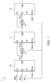
- FIG. 1 shows an exemplary embodiment of a scan chain.
- a scan chain 1 comprises a plurality of scan flip-flops and at least one combinatorial logic circuits coupled between two successively scan flip-flops.
- three scan flip-flops 10-12 and two combinatorial logic circuits (comb.) 13 and 14 are given as an example.
- the scan chain 1 performs scan testing to detect any manufacturing fault in these combinatorial logic circuits 13 and 14.
- Each of the scan flip-flops 10-12 has a test-in terminal TI, a data-in terminal DI, a clock-in terminal CK, and a data-out terminal DQ.
- the scan line 1 can selectively operate in a normal mode or a test mode in response to a test-enable signal STE.
- the test-enable terminals TE of the scan flip-flops 10-12 receive the same test-enable signal STE.
- the clock-in terminals CK of the scan flip-flops 10-12 receive clock signals CKA-CKC.
- the clock signals CKA-CKC are generated by different clock sources, and the timing of the clock signals CKA-CKC are the same or different.
- the clock signals CKA-CKC are generated by the same clock source, and the timing of the clock signals CKA-CKC are the same or different.
- the scan flip-flop 10 is the first one among the scan flip-flops 10-12.
- the data-in terminal DI of the scan flip-flop 10 receives a functional data signal S11 to serve as its data signal, and the test-in terminal TI thereof receives a scan test signal S10 to serve as its test signal.
- the flip-flop circuit 10 generates a scan-out signal S12 at its data-out terminal DQ, and the scan-out signal S12 is transmitted to the combinatorial logic circuit 13.
- the data-in terminal DI receives the signal output from the corresponding combinatorial logic circuit to serve as its data signal
- the test-in terminal TI receives the scan-out signal output from the data-out terminal DQ of the previously flip-flop circuit to serve as its test signal
- the scan-out signal output by the data-out terminal DQ is transmitted to the following combinatorial logic circuit.
- FIG. 2A shows one exemplary embodiment of a flip-flop circuit. At least one of the flip-flop circuits 10-12 shown in FIG. 1 may have the same structure shown in FIG. 2A , that is, at least one of the flip-flop circuits 10-12 may be implemented by the flip-flop circuit 2 of the embodiment of FIG. 2A .
- the flip-flop circuit 2 comprises a buffer 20 and a scan flip-flop 23.
- the scan flip-flop 23 comprises a multiplexer 21 and a D flip-flop 22.
- the buffer 20 receives a test signal STI from the test-in terminal TI of the flip-flop circuit 2 and generates a buffering signal S20.
- One input terminal (+) of the multiplexer 21 receives the buffering signal S20, and the other input terminal (-) thereof receives a data signal SDI from the data-in terminal DI of the flip-flop circuit 2.
- the multiplexer 21 is controlled by a test-enable signal STE from the test-enable terminal TE of the flip-flop circuit 2 to selectively transmit the buffering signal S20 or the data signal SDI to its output terminal to serve as an input signal S21.
- the input terminal (D) of the D flip-flop 22 receives the input signal S21, and the clock terminal (CK) is coupled to the clock terminal CK of the flip-flop circuit 2 to receive a corresponding clock signal CLK.
- the D flip-flop 22 operates based on the clock signal CLK to generate a scan-out signal S22 according to the input signal S21.
- the flip-flop circuit 2 transmits the scan-out signal S22 to the following circuit or device through its data-out terminal DQ.
- the buffer 20 has two power terminals 20A and 20B.
- the power terminal S20A receives a supply voltage VDD which is used to power the flip-flop circuit 2, while the power terminal S20B receives a test-enable reverse signal STEB which is generated internally to be the reverse of the test-enable signal STE.
- the test-enable reverse signal STEB is generated by the multiplexer 21.
- the test-enable signal STE and the test-enable reverse signal STEB are used for operating the test mode, and can be respectively seen as a first test-enable signal and a second test-enable signal.
- the flip-flop circuit 2 may comprise several buffers 20 coupled in series to obtain longer delay time for the test signal STI, as shown in FIG. 2B . Accordingly, the buffers 20 operate together to generate the buffering signal S20 according to the test signal STI.
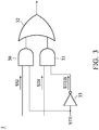
- FIG. 3 shows one exemplary embodiment of a multiplexer.
- the multiplexer 21 shown in FIG. 2A may have the same structure shown in FIG. 3 , that is, the multiplexer 21 may be implemented by the multiplexer 3 of the embodiment of FIG. 3 .
- the multiplexer 3 comprises AND gates 30 and 31, an OR gate 32, and an inverter 33.
- the input terminal of the inverter 33 receives the test-enable signal STE.
- the inverter 33 invers the test-enable signal STE to generate the test-enable reverse signal STEB.
- the test-enable reverse signal STEB is the reverse of the test-enable signal STE.
- One input terminal of the AND gate 30 receives a scan-in signal SSI, and the other input terminal thereof receives the test-enable signal STE.
- One input terminal of the AND gate 31 receives the data signal SDI, and the other input terminal thereof receives the test-enable reverse signal STEB.
- the input terminals of the OR gate 32 are coupled to the AND gates 30 and 31 to receives the signals output from the AND gates 30 and 31 to generate an output signal.
- the AND gate 30 receives the buffering signal S20 generated by the buffer 20 to serve as the scan-in signal SSI, and the OR gate 32 outputs its output signal to serve as the input signal S21.
- the test-enable reverse signal STEB is provided to the power terminal 20B of the buffer 20.
- FIG. 4 shows an exemplary embodiment of the buffer 20 (such as FIG. 2A and 2B shows).
- FIG. 4 also shows the inverter 33 in the multiplexer 3.
- the inverter 33 comprises a P-type metal-oxide-semiconductor (PMOS) transistor 330 and an N-type metal-oxide-semiconductor (NMOS) transistor 331.
- the gate of the PMOS transistor 330 receives the test-enable signal STE, the source thereof receives the supply voltage VDD, and the drain thereof is coupled to a node N30.
- PMOS P-type metal-oxide-semiconductor
- NMOS N-type metal-oxide-semiconductor
- the gate of the NMOS transistor 331 receives the test-enable signal STE, the drain thereof is coupled to the node N30, and the source thereof receives a supply voltage VSS which is used to power the flip-flop circuit 2.
- the supply voltage VSS is lower than the supply voltage VDD.
- the supply voltage VSS is a voltage of the ground.
- the test-enable reverse signal STEB is generated at the node N30.
- the buffers 20 comprises inverters 40 and 41.
- the inverter 40 is composed of a PMOS transistor 400 and an NMOS transistor 401.
- the gate of the PMOS transistor 400 receives the test signal STI, the source thereof is coupled to the power terminal 20A to receive the supply voltage VDD, and the drain thereof is coupled to a node N40.
- the gate of the NMOS transistor 401 receives the test signal STI, the drain thereof is coupled to the node N40, and the source thereof is coupled to the power terminal 20B to receive the test-enable reverse signal STEB.
- the inverter 41 is composed of a PMOS transistor 410 and an NMOS transistor 411.
- the gate of the PMOS transistor 410 is coupled to the node N40 to receive the signal S40, the source thereof is coupled to the power terminal 20A to receive the supply voltage VDD, and the drain thereof is coupled to a node N41.
- the gate of the NMOS transistor 411 is coupled to the node N40 to receive the signal S40, the drain thereof is coupled to the node N41, and the source thereof is coupled to the power terminal 20B to receive the test-enable reverse signal STEB.
- the buffering signal S20 is generated at the node N41.
- the scan line 1 when the test-enable signal STE is at a high voltage level, such as the level of the supply voltage VDD, the scan line 1 operates in the test mode.
- the test-enable reverse signal STEB is at a low voltage level, such as the level of the supply voltage VSS, during the test mode.
- the level of the signal S40 is the reverse of the test signal STI through the operation of the inverter 40, while the level of the buffering signal S20 is the reverse of the signal S40 through the operation of the inverter 41.
- the level of the buffering signal S20 varies with the variation in the voltage level of the test signal STI, and the phase of the buffering signal S20 is the same as the phase of the test signal STI.
- the phase of the buffering signal S20 is the same as the phase of the test signal STI.
- FIG. 4 there are two stacked NMOS transistors 401 and 331 between the node N40 and the supply voltage VSS.
- the delay time when the signal S40 is switched to the level of the supply level VSS from the level of the supply voltage VDD is enlarged due to the two stacked NMOS transistors 401 and 331.
- the falling delay (not shown) of the signal S40 is enlarged. Also referring to FIG.
- the multiplexer 21 transmits the buffering signal S20 to its output terminal according to the test-enable signal STE to serve as the input signal S21, and
- the D flip-flop 22 operates based on the clock signal CLK to generate the scan-out signal S22 according to the input signal S21.
- the scan line 1 when the test-enable signal STE is at the level of the supply voltage VSS, the scan line 1 operates in the normal mode.
- the test-enable reverse signal STEB is the level of the supply voltage VDD during the test mode.
- the test-enable signal STE is switched to the level of the supply voltage VSS from the level of the supply voltage VDD (that is, the test-enable reverse signal STEB is switched to the level of the supply voltage VDD from the level of the supply voltage VSS) during the period when the test signal STI is at the level of the supply voltage VDD, as shown in FIG. 5A .
- the NMOS transistor 401 is turned on.
- the level of the signal S40 starts increasing toward the level of the difference (VDD-Vtn) between the supply level VDD and the threshold Vtn of the NMOS transistor 401 and then increases toward the level of the supply level VDD from the level of the difference (VDD-Vtn).
- the level of the signal S40 is switched to the level of the supply voltage VDD. Then, the level of the signal S40 is kept at the level of the supply voltage VDD during the normal mode.
- the test-enable signal STE is switched to the level of the supply voltage VSS from the level of the supply voltage VDD (that is, the test-enable reverse signal STEB is switched to the level of the supply voltage VDD from the level of the supply voltage VSS) during the period when the test signal STI is at the level of the supply voltage VSS, as shown in FIG. 5B .
- the NMOS transistor 411 is turned on.
- the level of the buffering signal S20 starts increasing toward the level of the difference (VDD-Vtn) and then increases toward the level of the supply level VDD from the level of the difference (VDD-Vtn).
- the level of the buffering signal S20 After the level of the buffering signal S20 reaches the level of the supply voltage VDD during the normal mode, the level of the buffering signal S20 is kept at the level of the supply voltage VDD according to the test-enable reverse signal STEB with the level of the supply voltage VDD because the level of the voltage S40 is kept at the level of the supply voltage VDD to turn on the NMOS transistor 411.
- the level of one of the signal S40 and the buffering signal S20 has one transient, and the level of the other one is not changed, which decreases transient power of the buffer 2 during the normal mode.
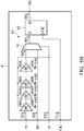
- FIG. 6A shows another exemplary embodiment of a flip-flop circuit.
- the flip-flop circuit 2 comprises a buffer 60 and a scan flip-flop 63.
- the scan flip-flop 63 comprises a multiplexer 61 and a D flip-flop 62.
- the connection between the buffer 60, the multiplexer 61, and the D flip-flop 62 and the signals received by them are similar to those in the embodiment of FIG. 2A . Thus, the description related to the similarity is omitted here.
- the difference between the flip-flop circuits 2 and 6 is that the power terminal S60A of the buffer 60 receives the enable signal STE and the power terminal S60B receives the supply voltage VSS.
- the multiplexer 61 shown in FIG. 6A may have the same structure shown in FIG. 3 , that is, the multiplexer 61 may be implemented by the multiplexer 3 of the embodiment of FIG. 3 .
- the structure of the multiplexer 3 has been described above, thus, the related description is omitted here.
- the AND gate 30 receives the buffering signal S60 generated by the buffer 60 to serve as the scan-in signal SSI, and the OR gate 32 outputs its output signal to serve as the input signal S61.
- the flip-flop circuit 6 may comprise several buffers 60 coupled in series to obtain longer delay time for the test signal STI, as shown in FIG. 6B . Accordingly, the buffers 60 operate together to generate the buffering signal S60 according to the test signal STI.
- FIG. 7 shows an exemplary embodiment of the buffer 60 (such as FIG. 6A and 6B shows).
- FIG. 7 also shows the inverter 33 in the multiplexer 3.
- the structure of the inverter 33 has been described above, thus, the related description is omitted here.
- the buffers 70 comprises inverters 70 and 71.
- the inverter 70 is composed of a PMOS transistor 700 and an NMOS transistor 701.
- the gate of the PMOS transistor 700 receives the test signal STI, the source thereof is coupled to the power terminal 60A to receive the test-enable signal STE, and the drain thereof is coupled to a node N70.
- the gate of the NMOS transistor 401 receives the test signal STI, the drain thereof is coupled to the node N70, and the source thereof is coupled to the power terminal 60B to receive the supply voltage VSS.
- the inverter 71 is composed of a PMOS transistor 710 and an NMOS transistor 711.
- the gate of the PMOS transistor 710 is coupled to the node N70 to receive the signal S70, the source thereof is coupled to the power terminal 60A to receive the test-enable signal STE, and the drain thereof is coupled to a node N71.
- the gate of the NMOS transistor 711 is coupled to the node N70 to receive the signal S70, the drain thereof is coupled to the node N71, and the source thereof is coupled to the power terminal 60B to receive the supply voltage VSS.
- the buffering signal S60 is generated at the node N71.
- the scan line 1 when the test-enable signal STE is at the level of the supply voltage VDD, the scan line 1 operates in the test mode.
- the level of the signal S70 is the reverse of the test signal STI through the operation of the inverter 70
- the level of the buffering signal S60 is the reverse of the signal S70 through the operation of the inverter 71.
- the level of the buffering signal S60 varies with the variation in the voltage level of the test signal STI
- the phase of the buffering signal S20 is the same as the phase of the test signal STI.
- the power terminal 60A receives the test-enable signal STE.
- the test-enable signal STE Since the test-enable signal STE is applied to all flip-flop circuits in the scan chain 1, the test-enable signal STE has weak driving strength. Thus, the delay time when the signal S70 is switched to the level of the supply level VDD from the level of the supply voltage VSS is enlarged due to the weak driving strength of the test-enable signal STE. In other words, during the test mode, the rising delay (not shown) of the signal S70 is enlarged. Based on the same reason, the delay time when the buffering signal S60 is switched to the level of the supply level VDD from the level of the supply voltage VSS is enlarged due to the weak driving strength of the test-enable signal STE. In other words, during the test mode, the rising delay (not shown) of the buffering signal S60 is enlarged.
- the delay time for the signal received by the flip-flop circuit 6 is also enlarged. Compared with a conventional delay chain, less buffers 60 are applied to achieve a predetermined delay time.
- the scan line 1 when the test-enable signal STE is at the level of the supply voltage VSS, the scan line 1 operates in the normal mode. In some cases, the test-enable signal STE is switched to the level of the supply voltage VSS from the level of the supply voltage VDD during the period when the test signal STI is at the level of the supply voltage VDD, as shown in FIG. 8A . Referring to FIG.
- the NMOS transistor 701 is turned on according to the test signal STI with the level of the supply voltage VDD, the level of the signal S70 is already at the level of the supply voltage VSS.
- the signal S70 is still kept at the level of the supply voltage VSS because of the level of the supply voltage VSS at both of the power terminals 60A and 60B.
- the PMOS transistor 710 is turned on.
- the level of the buffering signal S60 starts decreasing toward the level of the sum (VSS+Vtp) of the supply voltage VSS and the threshold Vtp of the PMOS transistor 700 and then decreases toward the level of the supply level VSS from the level of the sum (VSS+Vtp).
- the level of the buffering signal S60 After the level of the buffering signal S60 reaches the level of the supply voltage VSS during the normal mode, the level of the buffering signal S60 is kept at the level of the supply voltage VSS during the normal mode according to the test-enable signal STE with the level of the supply voltage VSS because the level of the voltage S70 is kept at the level of the supply voltage VSS to turn on the PMOS transistor 710.
- the test-enable signal STE is switched to the level of the supply voltage VSS from the level of the supply voltage VDD during the period when the test signal STI is at the level of the supply voltage VSS, as shown in FIG. 8B .
- the PMOS transistor 700 is turned on.
- the level of the signal S70 starts decreasing toward the level of the sum (VSS+Vtp) and then decreases toward the level of the supply level VSS from the level of the sum (VDD+Vtp).
- the level of the signal S70 is at the level of the supply voltage VSS. Then, the level of the signal S70 is kept at the level of the supply voltage VSS during the normal mode.
- the level of one of the signal S70 and the buffering signal S60 has one transient, and the level of the other is not changed, which decreases transient power of the buffer 6 during the normal mode.
- FIG. 9A shows another exemplary embodiment of a flip-flop circuit.
- the flip-flop circuit 9 comprises a buffer 90 and a scan flip-flop 93.
- the scan flip-flop 93 comprises a multiplexer 91 and a D flip-flop 92.
- the connection between the buffer 90, the multiplexer 91, and the D flip-flop 92 and the signals received by them are similar to those in the embodiment of FIG. 2A . Thus, the description related to the similarity is omitted here.
- the difference between the flip-flop circuits 2 and 9 is that the power terminal S90A of the buffer 90 receives the enable signal STE.
- the multiplexer 91 shown in FIG. 9A may have the same structure shown in FIG. 3 , that is, the multiplexer 91 may be implemented by the multiplexer 3 of the embodiment of FIG. 3 .
- the structure of the multiplexer 3 has been described above, thus, the related description is omitted here.
- the AND gate 30 receives the buffering signal S90 generated by the buffer 90 to serve as the scan-in signal SSI, and the OR gate 32 outputs its output signal to serve as the input signal S91.
- the flip-flop circuit 9 may comprise several buffers 90 coupled in series to obtain longer delay time for the test signal STI, as shown in FIG. 9B . Accordingly, the buffers 90 operate together to generate the buffering signal S90 according to the test signal STI.
- FIG. 10 shows an exemplary embodiment of the buffer 90 (such as FIG. 9A and 9B shows).
- FIG. 7 also shows the inverter 33 in the multiplexer 3. The structure of the inverter 33 has been described above, thus, the related description is omitted here.
- the buffers 100 comprises inverters 100 and 101.
- the inverter 100 is composed of a PMOS transistor 1000 and an NMOS transistor 1001.
- the gate of the PMOS transistor 1000 receives the test signal STI, the source thereof is coupled to the power terminal 90A to receive the test-enable signal STE, and the drain thereof is coupled to a node N100.
- the gate of the NMOS transistor 1001 receives the test signal STI, the drain thereof is coupled to the node N100, and the source thereof is coupled to the power terminal 90B to receive the test-enable reverse signal STEB.
- the inverter 101 is composed of a PMOS transistor 1010 and an NMOS transistor 1011.
- the gate of the PMOS transistor 1010 is coupled to the node N100 to receive the signal S100, the source thereof is coupled to the power terminal 90A to receive the test-enable signal STE, and the drain thereof is coupled to a node N101.
- the gate of the NMOS transistor 1011 is coupled to the node N100 to receive the signal S100, the drain thereof is coupled to the node N71, and the source thereof is coupled to the power terminal 90B to receive the test-enable reverse signal STEB.
- the buffering signal S90 is generated at the node N71.
- the scan line 1 when the test-enable signal STE is at the level of the supply voltage VDD, the scan line 1 operates in the test mode.
- the test-enable reverse signal STEB is at the level of the supply voltage VSS, during the test mode.
- the level of the signal S100 is the reverse of the test signal STI through the operation of the inverter 100
- the level of the buffering signal S90 is the reverse of the signal S100 through the operation of the inverter 101.
- the level of the buffering signal S900 varies with the variation in the voltage level of the test signal STI
- the phase of the buffering signal S90 is the same as the phase of the test signal STI.
- the scan line 1 when the test-enable signal STE is at the level of the supply voltage VSS, the scan line 1 operates in the normal mode.
- the test-enable reverse signal STEB is the level of the supply voltage VDD during the test mode.
- the test-enable signal STE is switched to the level of the supply voltage VSS from the level of the supply voltage VDD (that is, the test-enable reverse signal STEB is switched to the level of the supply voltage VDD from the level of the supply voltage VSS) during the period when the test signal STI is at the level of the supply voltage VSS, as shown in FIG. 11 . Referring to FIG.
- the level of the signal S100 is at the level of the supply voltage VDD according to the test-enable signal STE with the level of the supply voltage VDD.
- test-enable signal STE When the test-enable signal STE is switched to the level of the supply voltage VSS from the level of the supply voltage VDD during the period when the test signal STI is at the level of the supply voltage VSS, the signal S100 is switched to the level of the sum (VSS+Vtp) from the voltage of the supply voltage VDD.
- the signal S100 is switched to the level of the difference (VDD-Vtn) according to the test-enable reverse signal STEB with the voltage of the supply voltage VDD once the test signal STI is switched to the level of the supply voltage VDD, while the signal S100 is switched to the level of the sum (VSS+Vtp) according to the test-enable signal STE with the voltage of the supply voltage VSS once the test signal STI is switched to the level of the supply voltage VSS.
- the signal S100 is switched between the level of the difference (VDD-Vtn) and the level of the sum (VSS+Vtp).
- the buffering signal S90 is also switched between the level of the difference (VDD-Vtn) and the level of the sum (VSS+Vtp)
- the test-enable signal STE is switched to the level of the supply voltage VSS from the level of the supply voltage VDD (that is, the test-enable reverse signal STEB is switched to the level of the supply voltage VDD from the level of the supply voltage VSS) during the period when the test signal STI is at the level of the supply voltage VDD.
- both the signal S100 and the buffering signal S90 are switched between the level of the difference (VDD-Vtn) and the level of the sum (VSS+Vtp).
- the amplitude of the levels of the signal S100 and the buffering signal S90 during the normal mode is less that during the test mode, thereby decreasing the power consumption during the normal mode.
Landscapes
- Engineering & Computer Science (AREA)
- Physics & Mathematics (AREA)
- General Engineering & Computer Science (AREA)
- General Physics & Mathematics (AREA)
- Computer Hardware Design (AREA)
- Computing Systems (AREA)
- Mathematical Physics (AREA)
- Computer Networks & Wireless Communication (AREA)
- Tests Of Electronic Circuits (AREA)
- Semiconductor Integrated Circuits (AREA)
Abstract
Description
- This application claims the benefit of
U.S. Provisional Application No. 62/456,198, filed on February 8, 2017 - The invention relates to a flip-flop circuit, and more particularly, to a flip-flop circuit applied in a scan chain for testing.
- Scan chains are applied to detect various manufacturing faults in combinatorial logic blocks during test procedures. Generally, a scan chain is composed of several scan flip-flops which are coupled in series. However, due to process, voltage, and temperature (PVT) variation and clock skew, the hold-time violation of the scan flip-flop become more serious. Thus, to fix the hold-time violation, a delay chain composed of several buffers is added in the scan path between the data output terminal of one scan flip-flop and the scan-in terminal of the following scan flip-flop. These additional buffers would occupy large area of the circuit board. Moreover, these additional buffers would also consume unnecessary power, especially, when the scan chain operates in a normal mode.
- One exemplary embodiment of a flip-flop circuit is provided. The flip-flop circuit receives a test signal at a test-in terminal and a data signal at a data-in terminal and generates a scan-out signal. The flip-flop circuit comprises a buffer and a scan flip-flop. The buffer has an input terminal coupled to the test-in terminal and an output terminal and further has a first power terminal and a second power terminal. The buffer operates to generate a buffering signal. The scan flip-flop receives the buffering signal and the data signal. The scan flip-flop is controlled by a test-enable signal to generate the scan-out signal according to the buffering signal or the data signal. The scan flip-flop further generates a test-enable reverse signal which is the reverse of the test-enable signal. The first power terminal of the buffer receives the test-enable signal or the test-enable reverse signal.
- Another exemplary embodiment of a scan chain is provided. The scab chain comprises a first flip-flop circuit, a second flip-flop circuit, and a combinatorial logic circuit. Each of the first and second flip-flop circuits receives a test signal at a test-in terminal, receives a data signal at a data-in terminal, receives a teat-enable signal at a test-enable terminal, and generates a scan-out signal at a date-out terminal. The combinatorial logic circuit is coupled between the data-out terminal of the first flip-flop circuit and the data-in terminal of the second flip-flop circuit. The second flip-flop circuit receives the scan-out signal generated by the first flip-flop circuit through the corresponding the test-in terminal to serve as the test signal for the second flip-flop. Each of the first and second flip-flop circuits comprises a buffer and a scan flip-flop. The buffer has an input terminal coupled to the test-in terminal and an output terminal and further has a first power terminal and a second power terminal. The buffer operates to generate a buffering signal. The scan flip-flop receives the buffering signal and the data signal and controlled by the test-enable signal to generate the scan-out signal according to the buffering signal or the data signal. The scan flip-flop further generates a test-enable reverse signal which is the reverse of the test-enable signal. The first power terminal of the buffer receives the test-enable signal or the test-enable reverse signal.
- A detailed description is given in the following embodiments with reference to the accompanying drawings.
- The invention can be more fully understood by reading the subsequent detailed description and examples with references made to the accompanying drawings, wherein:
-
FIG. 1 shows an exemplary embodiment of a scan chain; -
FIG. 2A shows one exemplary embodiment of a flip-flop circuit; -
FIG. 2B shows another exemplary embodiment of a flip-flop circuit; -
FIG. 3 shows an exemplary embodiment of a multiplexer; -
FIG. 4 shows an exemplary embodiment of a buffer in the flip-flop circuit ofFIG. 2A ; -
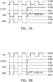
FIGs. 5A and 5B are schematic views showing timing chart of main signals of the flip-flop circuit ofFIG. 2A in various cases; -
FIG. 6A shows another exemplary embodiment of a flip-flop circuit; -
FIG. 6B shows another exemplary embodiment of a flip-flop circuit; -
FIG. 7 shows an exemplary embodiment of a buffer in the flip-flop circuit ofFIG. 6A ; -
FIGs. 8A and 8B are schematic views showing timing chart of main signals of the flip-flop circuit ofFIG. 6A in various cases; -
FIG. 9A shows another exemplary embodiment of a flip-flop circuit; -
FIG. 9B shows another exemplary embodiment of a flip-flop circuit; -
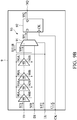
FIG. 10 shows an exemplary embodiment of a buffer in the flip-flop circuit ofFIG. 9A ; and -
FIG. 11 is a schematic view showing timing chart of main signals of the flip-flop circuit ofFIG. 9A in various cases. - The following description is of the best-contemplated mode of carrying out the invention. This description is made for the purpose of illustrating the general principles of the invention and should not be taken in a limiting sense. The scope of the invention is best determined by reference to the appended claims.
-
FIG. 1 shows an exemplary embodiment of a scan chain. As shown inFIG. 1 , ascan chain 1 comprises a plurality of scan flip-flops and at least one combinatorial logic circuits coupled between two successively scan flip-flops. In the embodiment ofFIG. 1 , three scan flip-flops 10-12 and two combinatorial logic circuits (comb.) 13 and 14 are given as an example. Thescan chain 1 performs scan testing to detect any manufacturing fault in thesecombinatorial logic circuits scan line 1 can selectively operate in a normal mode or a test mode in response to a test-enable signal STE. The test-enable terminals TE of the scan flip-flops 10-12 receive the same test-enable signal STE. The clock-in terminals CK of the scan flip-flops 10-12 receive clock signals CKA-CKC. In an embodiment, the clock signals CKA-CKC are generated by different clock sources, and the timing of the clock signals CKA-CKC are the same or different. In another embodiment, the clock signals CKA-CKC are generated by the same clock source, and the timing of the clock signals CKA-CKC are the same or different. The scan flip-flop 10 is the first one among the scan flip-flops 10-12. The data-in terminal DI of the scan flip-flop 10 receives a functional data signal S11 to serve as its data signal, and the test-in terminal TI thereof receives a scan test signal S10 to serve as its test signal. The flip-flop circuit 10 generates a scan-out signal S12 at its data-out terminal DQ, and the scan-out signal S12 is transmitted to thecombinatorial logic circuit 13. For each of the scan output flip-flops -
FIG. 2A shows one exemplary embodiment of a flip-flop circuit. At least one of the flip-flop circuits 10-12 shown inFIG. 1 may have the same structure shown inFIG. 2A , that is, at least one of the flip-flop circuits 10-12 may be implemented by the flip-flop circuit 2 of the embodiment ofFIG. 2A . As shown inFIG. 2A , the flip-flop circuit 2 comprises abuffer 20 and a scan flip-flop 23. The scan flip-flop 23 comprises amultiplexer 21 and a D flip-flop 22. Thebuffer 20 receives a test signal STI from the test-in terminal TI of the flip-flop circuit 2 and generates a buffering signal S20. One input terminal (+) of themultiplexer 21 receives the buffering signal S20, and the other input terminal (-) thereof receives a data signal SDI from the data-in terminal DI of the flip-flop circuit 2. Themultiplexer 21 is controlled by a test-enable signal STE from the test-enable terminal TE of the flip-flop circuit 2 to selectively transmit the buffering signal S20 or the data signal SDI to its output terminal to serve as an input signal S21. The input terminal (D) of the D flip-flop 22 receives the input signal S21, and the clock terminal (CK) is coupled to the clock terminal CK of the flip-flop circuit 2 to receive a corresponding clock signal CLK. The D flip-flop 22 operates based on the clock signal CLK to generate a scan-out signal S22 according to the input signal S21. The flip-flop circuit 2 transmits the scan-out signal S22 to the following circuit or device through its data-out terminal DQ. - Referring to
FIG. 2A , thebuffer 20 has twopower terminals flop circuit 2, while the power terminal S20B receives a test-enable reverse signal STEB which is generated internally to be the reverse of the test-enable signal STE. In the embodiment, the test-enable reverse signal STEB is generated by themultiplexer 21. The test-enable signal STE and the test-enable reverse signal STEB are used for operating the test mode, and can be respectively seen as a first test-enable signal and a second test-enable signal. - In the embodiment of
FIG. 2A , there is onebuffer 20 in the flip-flop circuit 2. However, in other embodiments, the flip-flop circuit 2 may compriseseveral buffers 20 coupled in series to obtain longer delay time for the test signal STI, as shown inFIG. 2B . Accordingly, thebuffers 20 operate together to generate the buffering signal S20 according to the test signal STI. -
FIG. 3 shows one exemplary embodiment of a multiplexer. Themultiplexer 21 shown inFIG. 2A may have the same structure shown inFIG. 3 , that is, themultiplexer 21 may be implemented by themultiplexer 3 of the embodiment ofFIG. 3 . Themultiplexer 3 comprises ANDgates OR gate 32, and aninverter 33. The input terminal of theinverter 33 receives the test-enable signal STE. Theinverter 33 invers the test-enable signal STE to generate the test-enable reverse signal STEB. Thus, the test-enable reverse signal STEB is the reverse of the test-enable signal STE. One input terminal of the ANDgate 30 receives a scan-in signal SSI, and the other input terminal thereof receives the test-enable signal STE. One input terminal of the ANDgate 31 receives the data signal SDI, and the other input terminal thereof receives the test-enable reverse signal STEB. The input terminals of theOR gate 32 are coupled to the ANDgates gates multiplexer 21 is implemented by themultiplexer 3, the ANDgate 30 receives the buffering signal S20 generated by thebuffer 20 to serve as the scan-in signal SSI, and theOR gate 32 outputs its output signal to serve as the input signal S21. The test-enable reverse signal STEB is provided to thepower terminal 20B of thebuffer 20. -
FIG. 4 shows an exemplary embodiment of the buffer 20 (such asFIG. 2A and2B shows). In order to illustrate the structure and operation of thebuffer 20,FIG. 4 also shows theinverter 33 in themultiplexer 3. Referring toFIG. 4 , theinverter 33 comprises a P-type metal-oxide-semiconductor (PMOS)transistor 330 and an N-type metal-oxide-semiconductor (NMOS)transistor 331. The gate of thePMOS transistor 330 receives the test-enable signal STE, the source thereof receives the supply voltage VDD, and the drain thereof is coupled to a node N30. The gate of theNMOS transistor 331 receives the test-enable signal STE, the drain thereof is coupled to the node N30, and the source thereof receives a supply voltage VSS which is used to power the flip-flop circuit 2. In the embodiment, the supply voltage VSS is lower than the supply voltage VDD. For example, the supply voltage VSS is a voltage of the ground. The test-enable reverse signal STEB is generated at the node N30. - Also referring to
FIG. 4 , thebuffers 20 comprisesinverters inverter 40 is composed of aPMOS transistor 400 and anNMOS transistor 401. The gate of thePMOS transistor 400 receives the test signal STI, the source thereof is coupled to thepower terminal 20A to receive the supply voltage VDD, and the drain thereof is coupled to a node N40. The gate of theNMOS transistor 401 receives the test signal STI, the drain thereof is coupled to the node N40, and the source thereof is coupled to thepower terminal 20B to receive the test-enable reverse signal STEB. There is a signal S40 generated at the node N40. Theinverter 41 is composed of aPMOS transistor 410 and anNMOS transistor 411. The gate of thePMOS transistor 410 is coupled to the node N40 to receive the signal S40, the source thereof is coupled to thepower terminal 20A to receive the supply voltage VDD, and the drain thereof is coupled to a node N41. The gate of theNMOS transistor 411 is coupled to the node N40 to receive the signal S40, the drain thereof is coupled to the node N41, and the source thereof is coupled to thepower terminal 20B to receive the test-enable reverse signal STEB. The buffering signal S20 is generated at the node N41. - Referring to
FIGs. 4 and5A-5B , when the test-enable signal STE is at a high voltage level, such as the level of the supply voltage VDD, thescan line 1 operates in the test mode. Through the operation of theinverter 33, the test-enable reverse signal STEB is at a low voltage level, such as the level of the supply voltage VSS, during the test mode. As shown inFIGs. 5A and 5B , during the test mode, the level of the signal S40 is the reverse of the test signal STI through the operation of theinverter 40, while the level of the buffering signal S20 is the reverse of the signal S40 through the operation of theinverter 41. Thus, the level of the buffering signal S20 varies with the variation in the voltage level of the test signal STI, and the phase of the buffering signal S20 is the same as the phase of the test signal STI. Referring toFIG. 4 , there are twostacked NMOS transistors stacked NMOS transistors FIG. 4 , there are twostacked NMOS transistors stacked NMOS transistors FIG. 2A , at the test mode, themultiplexer 21 transmits the buffering signal S20 to its output terminal according to the test-enable signal STE to serve as the input signal S21, and The D flip-flop 22 operates based on the clock signal CLK to generate the scan-out signal S22 according to the input signal S21. - As described above, for one flip-
flop circuit 2, since the falling delay of each of the signal S40 and the buffering signal S20 is enlarged, the delay time for the signal received by the flip-flop circuit 2 is also enlarged. Compared with a conventional delay chain,less buffers 20 are applied to achieve a predetermined delay time, - Referring to
FIGs. 4 and5A-5B , when the test-enable signal STE is at the level of the supply voltage VSS, thescan line 1 operates in the normal mode. Through the operation of theinverter 33, the test-enable reverse signal STEB is the level of the supply voltage VDD during the test mode. In some cases, the test-enable signal STE is switched to the level of the supply voltage VSS from the level of the supply voltage VDD (that is, the test-enable reverse signal STEB is switched to the level of the supply voltage VDD from the level of the supply voltage VSS) during the period when the test signal STI is at the level of the supply voltage VDD, as shown inFIG. 5A . Referring toFIG. 5A , during the period when the test signal STI is at the level of the supply voltage VDD, theNMOS transistor 401 is turned on. In response to the level switching of the test-enable reverse signal STEB, the level of the signal S40 starts increasing toward the level of the difference (VDD-Vtn) between the supply level VDD and the threshold Vtn of theNMOS transistor 401 and then increases toward the level of the supply level VDD from the level of the difference (VDD-Vtn). Once the test signal STI is switched to the level of the supply voltage VSS from the level of the supply voltage VDD to turn on thePMOS transistor 400, the level of the signal S40 is switched to the level of the supply voltage VDD. Then, the level of the signal S40 is kept at the level of the supply voltage VDD during the normal mode. - Also referring to
FIG. 5A , in the short period occurring before the time point when the test-enable reverse signal STEB is switched to the level of the supply voltage VDD from the level of the supply voltage VSS (that is, before the time point when thescan chain 1 enters the normal mode from the test mode), since thePMOS transistor 410 is turned on according to the signal S40 with the level of the supply voltage VSS, the level of the buffering signal S20 is already at the level of the supply voltage VDD. During the test mode, since theNMOS transistor 411 is continuously turned on by the signal S40, the level of the buffering signal S20 is still kept at the level of the supply voltage VDD in response to test-enable reverse signal STEB. - In some cases, the test-enable signal STE is switched to the level of the supply voltage VSS from the level of the supply voltage VDD (that is, the test-enable reverse signal STEB is switched to the level of the supply voltage VDD from the level of the supply voltage VSS) during the period when the test signal STI is at the level of the supply voltage VSS, as shown in
FIG. 5B . Referring toFIG. 5B , in the short period occurring before the time point when the test-enable reverse signal STEB is switched to the level of the supply voltage VDD from the level of the supply voltage VSS (that is, before the time point when thescan chain 1 enters the normal mode from the test mode), since thePMOS transistor 400 is turned on according to the test signal STI with the level of the supply voltage VSS, the level of the signal S40 is already at the level of the supply voltage VDD. During the normal mode, no matter what level the test signal STI is at, the signal S40 is still kept at the level of the supply voltage VDD because of the level of the supply voltage VDD at both of thepower terminals - Also referring to
FIG. 5B , during the period when the signal S40 is at the level of the supply voltage VDD, theNMOS transistor 411 is turned on. In response to the level switching of the test-enable reverse signal STEB, the level of the buffering signal S20 starts increasing toward the level of the difference (VDD-Vtn) and then increases toward the level of the supply level VDD from the level of the difference (VDD-Vtn). After the level of the buffering signal S20 reaches the level of the supply voltage VDD during the normal mode, the level of the buffering signal S20 is kept at the level of the supply voltage VDD according to the test-enable reverse signal STEB with the level of the supply voltage VDD because the level of the voltage S40 is kept at the level of the supply voltage VDD to turn on theNMOS transistor 411. - According to the above, when the
scan chain 1 enters the normal mode, the level of one of the signal S40 and the buffering signal S20 has one transient, and the level of the other one is not changed, which decreases transient power of thebuffer 2 during the normal mode. -
FIG. 6A shows another exemplary embodiment of a flip-flop circuit. At least one of the flip-flop circuits 10-12 shown inFIG. 1 may have the same structure shown inFIG. 6A , that is, at least one of the flip-flop circuits 10-12 may be implemented by the flip-flop circuit 6 of the embodiment ofFIG. 6A . As shown inFIG. 6A , the flip-flop circuit 2 comprises abuffer 60 and a scan flip-flop 63. The scan flip-flop 63 comprises amultiplexer 61 and a D flip-flop 62. The connection between thebuffer 60, themultiplexer 61, and the D flip-flop 62 and the signals received by them are similar to those in the embodiment ofFIG. 2A . Thus, the description related to the similarity is omitted here. The difference between the flip-flop circuits buffer 60 receives the enable signal STE and the power terminal S60B receives the supply voltage VSS. - The
multiplexer 61 shown inFIG. 6A may have the same structure shown inFIG. 3 , that is, themultiplexer 61 may be implemented by themultiplexer 3 of the embodiment ofFIG. 3 . The structure of themultiplexer 3 has been described above, thus, the related description is omitted here. In the embodiment where themultiplexer 61 is implemented by themultiplexer 3, the ANDgate 30 receives the buffering signal S60 generated by thebuffer 60 to serve as the scan-in signal SSI, and theOR gate 32 outputs its output signal to serve as the input signal S61. - In the embodiment of
FIG. 6A , there is onebuffer 60 in the flip-flop circuit 6. However, in other embodiments, the flip-flop circuit 6 may compriseseveral buffers 60 coupled in series to obtain longer delay time for the test signal STI, as shown inFIG. 6B . Accordingly, thebuffers 60 operate together to generate the buffering signal S60 according to the test signal STI. -
FIG. 7 shows an exemplary embodiment of the buffer 60 (such asFIG. 6A and6B shows). In order to illustrate the structure and operation of thebuffer 60,FIG. 7 also shows theinverter 33 in themultiplexer 3. The structure of theinverter 33 has been described above, thus, the related description is omitted here. - Also referring to
FIG. 7 , thebuffers 70 comprisesinverters inverter 70 is composed of aPMOS transistor 700 and anNMOS transistor 701. The gate of thePMOS transistor 700 receives the test signal STI, the source thereof is coupled to thepower terminal 60A to receive the test-enable signal STE, and the drain thereof is coupled to a node N70. The gate of theNMOS transistor 401 receives the test signal STI, the drain thereof is coupled to the node N70, and the source thereof is coupled to thepower terminal 60B to receive the supply voltage VSS. There is a signal S70 generated at the node N70. Theinverter 71 is composed of aPMOS transistor 710 and anNMOS transistor 711. The gate of thePMOS transistor 710 is coupled to the node N70 to receive the signal S70, the source thereof is coupled to thepower terminal 60A to receive the test-enable signal STE, and the drain thereof is coupled to a node N71. The gate of theNMOS transistor 711 is coupled to the node N70 to receive the signal S70, the drain thereof is coupled to the node N71, and the source thereof is coupled to thepower terminal 60B to receive the supply voltage VSS. The buffering signal S60 is generated at the node N71. - Referring to
FIGs. 7 and8A-8B , when the test-enable signal STE is at the level of the supply voltage VDD, thescan line 1 operates in the test mode. As shown inFIGs. 8A and 8B , during the test mode, the level of the signal S70 is the reverse of the test signal STI through the operation of theinverter 70, while the level of the buffering signal S60 is the reverse of the signal S70 through the operation of theinverter 71. Thus, the level of the buffering signal S60 varies with the variation in the voltage level of the test signal STI, and the phase of the buffering signal S20 is the same as the phase of the test signal STI. Referring toFIG. 7 , thepower terminal 60A receives the test-enable signal STE. Since the test-enable signal STE is applied to all flip-flop circuits in thescan chain 1, the test-enable signal STE has weak driving strength. Thus, the delay time when the signal S70 is switched to the level of the supply level VDD from the level of the supply voltage VSS is enlarged due to the weak driving strength of the test-enable signal STE. In other words, during the test mode, the rising delay (not shown) of the signal S70 is enlarged. Based on the same reason, the delay time when the buffering signal S60 is switched to the level of the supply level VDD from the level of the supply voltage VSS is enlarged due to the weak driving strength of the test-enable signal STE. In other words, during the test mode, the rising delay (not shown) of the buffering signal S60 is enlarged. - As described above, for one flip-
flop circuit 6, since the rising delay of each of the signal S70 and the buffering signal S60 is enlarged, the delay time for the signal received by the flip-flop circuit 6 is also enlarged. Compared with a conventional delay chain,less buffers 60 are applied to achieve a predetermined delay time. - Referring to
FIGs. 7 and8A-8B , when the test-enable signal STE is at the level of the supply voltage VSS, thescan line 1 operates in the normal mode. In some cases, the test-enable signal STE is switched to the level of the supply voltage VSS from the level of the supply voltage VDD during the period when the test signal STI is at the level of the supply voltage VDD, as shown inFIG. 8A . Referring toFIG. 8A , in the short period occurring before the time point when the test-enable signal STE is switched to the level of the supply voltage VSS from the level of the supply voltage VDD (that is, before the time point when thescan chain 1 enters the normal mode from the test mode), since theNMOS transistor 701 is turned on according to the test signal STI with the level of the supply voltage VDD, the level of the signal S70 is already at the level of the supply voltage VSS. During the normal mode, no matter what level the test signal STI is at, the signal S70 is still kept at the level of the supply voltage VSS because of the level of the supply voltage VSS at both of thepower terminals - Also referring to
FIG. 8A , during the period when the signal S70 is at the level of the supply voltage VSS, thePMOS transistor 710 is turned on. In response to the level switching of the test-enable signal STE, the level of the buffering signal S60 starts decreasing toward the level of the sum (VSS+Vtp) of the supply voltage VSS and the threshold Vtp of thePMOS transistor 700 and then decreases toward the level of the supply level VSS from the level of the sum (VSS+Vtp). After the level of the buffering signal S60 reaches the level of the supply voltage VSS during the normal mode, the level of the buffering signal S60 is kept at the level of the supply voltage VSS during the normal mode according to the test-enable signal STE with the level of the supply voltage VSS because the level of the voltage S70 is kept at the level of the supply voltage VSS to turn on thePMOS transistor 710. - In some cases, the test-enable signal STE is switched to the level of the supply voltage VSS from the level of the supply voltage VDD during the period when the test signal STI is at the level of the supply voltage VSS, as shown in
FIG. 8B . Referring toFIG. 8B , during the period when the test signal STI is at the level of the supply voltage VSS, thePMOS transistor 700 is turned on. In response to the level switching of the test-enable signal STE, the level of the signal S70 starts decreasing toward the level of the sum (VSS+Vtp) and then decreases toward the level of the supply level VSS from the level of the sum (VDD+Vtp). Once the test signal STI is switched to the level of the supply voltage VDD from the level of the supply voltage VSS to turn on theNMOS transistor 701, the level of the signal S70 is at the level of the supply voltage VSS. Then, the level of the signal S70 is kept at the level of the supply voltage VSS during the normal mode. - Also referring to
FIG. 8B , in the short period occurring before the time point when the test-enable signal STE is switched to the level of the supply voltage VSS from the level of the supply voltage VDD (that is, before the time point when thescan chain 1 enters the normal mode from the test mode), since theNMOS transistor 711 is turned on according to the signal S70 with the level of the supply voltage VDD, the level of the buffering signal S60 is already at the level of the supply voltage VSS. During the normal mode, since thePMOS transistor 710 is continuously turned on by the signal S70, the level of the buffering signal S60 is still kept at the level of the supply voltage VSS in response to the test-enable signal STE. - According to the above, when the
scan chain 1 enters the normal mode, the level of one of the signal S70 and the buffering signal S60 has one transient, and the level of the other is not changed, which decreases transient power of thebuffer 6 during the normal mode. -
FIG. 9A shows another exemplary embodiment of a flip-flop circuit. At least one of the flip-flop circuits 10-12 shown inFIG. 1 may have the same structure shown inFIG. 9A , that is, at least one of the flip-flop circuits 10-12 may be implemented by the flip-flop circuit 9 of the embodiment ofFIG. 9A . As shown inFIG. 9A , the flip-flop circuit 9 comprises abuffer 90 and a scan flip-flop 93. The scan flip-flop 93 comprises amultiplexer 91 and a D flip-flop 92. The connection between thebuffer 90, themultiplexer 91, and the D flip-flop 92 and the signals received by them are similar to those in the embodiment ofFIG. 2A . Thus, the description related to the similarity is omitted here. The difference between the flip-flop circuits buffer 90 receives the enable signal STE. - The
multiplexer 91 shown inFIG. 9A may have the same structure shown inFIG. 3 , that is, themultiplexer 91 may be implemented by themultiplexer 3 of the embodiment ofFIG. 3 . The structure of themultiplexer 3 has been described above, thus, the related description is omitted here. In the embodiment where themultiplexer 91 is implemented by themultiplexer 3, the ANDgate 30 receives the buffering signal S90 generated by thebuffer 90 to serve as the scan-in signal SSI, and theOR gate 32 outputs its output signal to serve as the input signal S91. - In the embodiment of
FIG. 9A , there is onebuffer 90 in the flip-flop circuit 9. However, in other embodiments, the flip-flop circuit 9 may compriseseveral buffers 90 coupled in series to obtain longer delay time for the test signal STI, as shown inFIG. 9B . Accordingly, thebuffers 90 operate together to generate the buffering signal S90 according to the test signal STI. -
FIG. 10 shows an exemplary embodiment of the buffer 90 (such asFIG. 9A and9B shows). In order to illustrate the structure and operation of thebuffer 90,FIG. 7 also shows theinverter 33 in themultiplexer 3. The structure of theinverter 33 has been described above, thus, the related description is omitted here. - Also referring to
FIG. 10 , thebuffers 100 comprisesinverters inverter 100 is composed of aPMOS transistor 1000 and anNMOS transistor 1001. The gate of thePMOS transistor 1000 receives the test signal STI, the source thereof is coupled to thepower terminal 90A to receive the test-enable signal STE, and the drain thereof is coupled to a node N100. The gate of theNMOS transistor 1001 receives the test signal STI, the drain thereof is coupled to the node N100, and the source thereof is coupled to thepower terminal 90B to receive the test-enable reverse signal STEB. There is a signal S100 generated at the node N100. Theinverter 101 is composed of aPMOS transistor 1010 and anNMOS transistor 1011. The gate of thePMOS transistor 1010 is coupled to the node N100 to receive the signal S100, the source thereof is coupled to thepower terminal 90A to receive the test-enable signal STE, and the drain thereof is coupled to a node N101. The gate of theNMOS transistor 1011 is coupled to the node N100 to receive the signal S100, the drain thereof is coupled to the node N71, and the source thereof is coupled to thepower terminal 90B to receive the test-enable reverse signal STEB. The buffering signal S90 is generated at the node N71. - Referring to
FIGs. 10 and11 , when the test-enable signal STE is at the level of the supply voltage VDD, thescan line 1 operates in the test mode. Through theinverter 33, the test-enable reverse signal STEB is at the level of the supply voltage VSS, during the test mode. As shown inFIG. 10 , during the test mode, the level of the signal S100 is the reverse of the test signal STI through the operation of theinverter 100, while the level of the buffering signal S90 is the reverse of the signal S100 through the operation of theinverter 101. Thus, the level of the buffering signal S900 varies with the variation in the voltage level of the test signal STI, and the phase of the buffering signal S90 is the same as the phase of the test signal STI. - Referring to
FIGs. 10 and11 , when the test-enable signal STE is at the level of the supply voltage VSS, thescan line 1 operates in the normal mode. Through theinverter 33, the test-enable reverse signal STEB is the level of the supply voltage VDD during the test mode. In some cases, the test-enable signal STE is switched to the level of the supply voltage VSS from the level of the supply voltage VDD (that is, the test-enable reverse signal STEB is switched to the level of the supply voltage VDD from the level of the supply voltage VSS) during the period when the test signal STI is at the level of the supply voltage VSS, as shown inFIG. 11 . Referring toFIG. 11 , in the short period occurring before the time point when the test-enable signal STE is switched to the level of the supply voltage VSS from the level of the supply voltage VDD (that is, before the time point when thescan chain 1 enters the normal mode from the test mode), since thePMOS transistor 1000 is turned on according to the test signal STI with the level of the supply voltage VSS, the level of the signal S100 is at the level of the supply voltage VDD according to the test-enable signal STE with the level of the supply voltage VDD. When the test-enable signal STE is switched to the level of the supply voltage VSS from the level of the supply voltage VDD during the period when the test signal STI is at the level of the supply voltage VSS, the signal S100 is switched to the level of the sum (VSS+Vtp) from the voltage of the supply voltage VDD. During the test mode, the signal S100 is switched to the level of the difference (VDD-Vtn) according to the test-enable reverse signal STEB with the voltage of the supply voltage VDD once the test signal STI is switched to the level of the supply voltage VDD, while the signal S100 is switched to the level of the sum (VSS+Vtp) according to the test-enable signal STE with the voltage of the supply voltage VSS once the test signal STI is switched to the level of the supply voltage VSS. In other words, during the normal mode, the signal S100 is switched between the level of the difference (VDD-Vtn) and the level of the sum (VSS+Vtp). - Also referring to
FIG. 11 , during the normal mode, through the operation of theinverter 101 based on the signal S100 and the test-enable signals STE and the test-enable reverse signal STEB, the buffering signal S90 is also switched between the level of the difference (VDD-Vtn) and the level of the sum (VSS+Vtp) - In some cases, the test-enable signal STE is switched to the level of the supply voltage VSS from the level of the supply voltage VDD (that is, the test-enable reverse signal STEB is switched to the level of the supply voltage VDD from the level of the supply voltage VSS) during the period when the test signal STI is at the level of the supply voltage VDD. During the normal mode, through the
operation buffer 90, both the signal S100 and the buffering signal S90 are switched between the level of the difference (VDD-Vtn) and the level of the sum (VSS+Vtp). - According to the above embodiment, the amplitude of the levels of the signal S100 and the buffering signal S90 during the normal mode is less that during the test mode, thereby decreasing the power consumption during the normal mode.
- While the invention has been described by way of example and in terms of the preferred embodiments, it is to be understood that the invention is not limited to the disclosed embodiments. On the contrary, it is intended to cover various modifications and similar arrangements (as would be apparent to those skilled in the art). Therefore, the scope of the appended claims should be accorded the broadest interpretation so as to encompass all such modifications and similar arrangements.
Claims (15)
- A flip-flop circuit for receiving a test signal at a test-in terminal and a data signal at a data-in terminal and generating a scan-out signal, comprising:a buffer having an input terminal coupled to the test-in terminal and an output terminal and further having a first power terminal and a second power terminal, wherein the buffer operates to generate a buffering signal; anda scan flip-flop receiving the buffering signal and the data signal and controlled by a test-enable signal to generate the scan-out signal according to the buffering signal or the data signal,wherein the scan flip-flop further generates a test-enable reverse signal which is the reverse of the test-enable signal, andwherein the first power terminal of the buffer receives the test-enable signal or the test-enable reverse signal.
- The flip-flop circuit as claimed in claim 1,
wherein the first power terminal of the buffer receives the test-enable reverse signal, and the second power terminal of the buffer receives a high supply voltage;
wherein the buffer comprises:a first P-type transistor having a gate terminal coupled to the input terminal of the buffer, a source terminal coupled to the second power terminal, and a drain terminal coupled to a first node;a first N-type transistor having a gate coupled to the input terminal of the buffer, a drain terminal coupled to the first node, and a source coupled to the first power terminal;a second P-type transistor having a gate terminal coupled to the first node, a source terminal coupled to the second power terminal, and a drain terminal coupled to the output terminal of the buffer; anda second N-type transistor having a gate coupled to the first node, a drain terminal coupled to the output terminal of the buffer, and a source coupled to the first power terminal. - The scan output flip-flop as claimed in claim 1,
wherein the first power terminal of the buffer receives the test-enable signal, and the second power terminal of the buffer receives a low supply voltage;
wherein the buffer comprises:a first P-type transistor having a gate terminal coupled to the input terminal of the buffer, a source terminal coupled to the first power terminal, and a drain terminal coupled to a first node;a first N-type transistor having a gate coupled to the input terminal of the buffer, a drain terminal coupled to the first node, and a source coupled to the second power terminal;a second P-type transistor having a gate terminal coupled to the first node, a source terminal coupled to the first power terminal, and a drain terminal coupled to the output terminal of the buffer; anda second N-type transistor having a gate coupled to the first node, a drain terminal coupled to the output terminal of the buffer, and a source coupled to the second power terminal. - The flip-flop circuit as claimed in claim 1,
wherein the first power terminal of the buffer receives the test-enable signal, and the second power terminal of the buffer receives the test-enable reverse signal;
wherein the buffer comprises:a first P-type transistor having a gate terminal coupled to the input terminal of the buffer, a source terminal coupled to the first power terminal, and a drain terminal coupled to a first node;a first N-type transistor having a gate coupled to the input terminal of the buffer, a drain terminal coupled to the first node, and a source coupled to the second power terminal;a second P-type transistor having a gate terminal coupled to the first node, a source terminal coupled to the first power terminal, and a drain terminal coupled to the output terminal of the buffer; anda second N-type transistor having a gate coupled to the first node, a drain terminal coupled to the output terminal of the buffer, and a source coupled to the second power terminal. - The flip-flop circuit claimed in claim 1,
wherein the flip-flop circuit is powered by a high supply voltage and a low supply voltage which is lower than the high supply voltage,
wherein the first power terminal of the buffer receives the test-enable reverse signal, and the second power terminal of the bufffer receives the high supply voltage. - The flip-flop circuit claimed in claim 1,
wherein the flip-flop circuit is powered by a high supply voltage and a low supply voltage which is lower than the high supply voltage,
wherein the first power terminal of the buffer receives the test-enable signal, and the second power terminal of the bufffer receives the low supply voltage. - The flip-flop circuit claimed in claim 1,
wherein the flip-flop circuit is powered by a high supply voltage and a low supply voltage which is lower than the high supply voltage,
wherein the first power terminal of the buffer receives the test-enable signal, and the second power terminal of the bufffer receives the test-enable reverse signal. - The flip-flop circuit as claimed in claim 1, wherein the scan flip-flop comprises:an inverter receiving the test-enable signal and generating the test-enable reverse signal;a first AND gate having a first input terminal receiving the buffering signal, a second input terminal receiving the second test signal, and an output terminal;a second AND gate having a first input terminal receiving the data signal, a second input terminal receiving the second test signal, and an output terminal generatingan OR gate having a first input terminal coupled to the output terminal of the first AND gate, a second input terminal coupled to the output terminal of the second AND gate, and an output terminal generating an input terminal; anda flip-flop receiving the input signal and generating the scan-out signal according to the input signal.
- A scan chain comprising:a first flip-flop circuit and a second flip-flop circuit, each of the first and second flip-flop circuits receiving a test signal at a test-in terminal, receiving a data signal at a data-in terminal, receiving a test-enable signal at a test-enable terminal, and generating a scan-out signal at a date-out terminal; anda combinatorial logic circuit, coupled between the data-out terminal of the first flip-flop circuit and the data-in terminal of the second flip-flop circuit,wherein the second flip-flop circuit receives the scan-out signal generated by the first flip-flop circuit through the corresponding the test-in terminal to serve as the test signal for the second flip-flop, and
wherein each of the first and second flip-flop circuits comprises:a buffer having an input terminal coupled to the test-in terminal from the test-in terminal and an output terminal and further having a first power terminal and a second power terminal, wherein the buffer operates to generate a buffering signal; anda scan flip-flop receiving the buffering signal and the data signal and controlled by the test-enable signal to generate the scan-out signal according to the buffering signal or the data signal,wherein the scan flip-flop further generates a test-enable reverse signal which is the reverse of the test-enable signal, andwherein the first power terminal of the buffer receives the test-enable signal or the test-enable reverse signal. - The scan chain as claimed in claim 9,
wherein for each of the first and second flip-flop circuits, the first power terminal of the buffer receives the test-enable reverse signal, and the second power terminal of the buffer receives a high supply voltage;
wherein for each of the first and second flip-flop circuits, the buffer comprises:a first P-type transistor having a gate terminal coupled to the input terminal of the buffer, a source terminal coupled to the second power terminal, and a drain terminal coupled to a first node (N40);a first N-type transistor having a gate coupled to the input terminal of the buffer, a drain terminal coupled to the first node, and a source coupled to the first power terminal;a second P-type transistor having a gate terminal coupled to the first node, a source terminal coupled to the second power terminal, and a drain terminal coupled to the output terminal of the buffer; anda second N-type transistor having a gate coupled to the first node, a drain terminal coupled to the output terminal of the buffer, and a source coupled to the first power terminal. - The scan chain as claimed in claim 9,
wherein for each of the first and second flip-flop circuits, the first power terminal of the buffer receives the test-enable signal, and the second power terminal of the buffer receives a low supply voltage;
wherein for each of the first and second flip-flop circuits, the buffer comprises:a first P-type transistor having a gate terminal coupled to the input terminal of the buffer, a source terminal coupled to the first power terminal, and a drain terminal coupled to a first node;a first N-type transistor having a gate coupled to the input terminal of the buffer, a drain terminal coupled to the first node, and a source coupled to the second power terminal;a second P-type transistor having a gate terminal coupled to the first node, a source terminal coupled to the first power terminal, and a drain terminal coupled to the output terminal of the buffer; anda second N-type transistor having a gate coupled to the first node, a drain terminal coupled to the output terminal of the buffer, and a source coupled to the second power terminal. - The scan chain as claimed in claim 9,
wherein for each of the first and second flip-flop circuits, the first power terminal of the buffer receives the test-enable signal, and the second power terminal of the buffer receives the test-enable reverse signal;
wherein for each of the first and second flip-flop circuits, the buffer comprises:a first P-type transistor having a gate terminal coupled to the input terminal of the buffer, a source terminal coupled to the first power terminal, and a drain terminal coupled to a first node;a first N-type transistor having a gate coupled to the input terminal of the buffer, a drain terminal coupled to the first node, and a source coupled to the second power terminal;a second P-type transistor having a gate terminal coupled to the first node, a source terminal coupled to the first power terminal, and a drain terminal coupled to the output terminal of the buffer; anda second N-type transistor having a gate coupled to the first node, a drain terminal coupled to the output terminal of the buffer, and a source coupled to the second power terminal. - The scan chain claimed in claim 9,
wherein the first and second flip-flop circuits are powered by a high supply voltage and a low supply voltage which is lower than the high supply voltage,
wherein for each of the first and second flip-flop circuits, the first power terminal of the buffer receives the test-enable reverse signal, and the second power terminal of the bufffer receives the high supply voltage. - The scan chain claimed in claim 9,
wherein the first and second flip-flop circuits are powered by a high supply voltage and a low supply voltage which is lower than the high supply voltage,
wherein for each of the first and second flip-flop circuits, the first power terminal of the buffer receives the test-enable signal, and the second power terminal of the bufffer receives the low supply voltage or the the test-enable reverse signal. - The scan chain as claimed in claim 9, wherein for each of the first and second flip-flop circuits, the scan flip-flop comprises:an inverter receiving the test-enable signal and generating the test-enable reverse signal;a first AND gate having a first input terminal receiving the buffering signal, a second input terminal receiving the second test signal, and an output terminal;a second AND gate having a first input terminal receiving the data signal, a second input terminal receiving the second test signal, and an output terminal generatingan OR gate having a first input terminal coupled to the output terminal of the first AND gate, a second input terminal coupled to the output terminal of the second AND gate, and an output terminal generating an input terminal; anda flip-flop receiving the input signal and generating the scan-out signal according to the input signal.
Applications Claiming Priority (2)
| Application Number | Priority Date | Filing Date | Title |
|---|---|---|---|
| US201762456198P | 2017-02-08 | 2017-02-08 | |
| US15/647,485 US10126363B2 (en) | 2017-02-08 | 2017-07-12 | Flip-flop circuit and scan chain using the same |
Publications (2)
| Publication Number | Publication Date |
|---|---|
| EP3361274A1 true EP3361274A1 (en) | 2018-08-15 |
| EP3361274B1 EP3361274B1 (en) | 2019-08-21 |
Family
ID=60673504
Family Applications (1)
| Application Number | Title | Priority Date | Filing Date |
|---|---|---|---|
| EP17207000.5A Active EP3361274B1 (en) | 2017-02-08 | 2017-12-13 | Flip-flop circuit and scan chain using the same |
Country Status (4)
| Country | Link |
|---|---|
| US (1) | US10126363B2 (en) |
| EP (1) | EP3361274B1 (en) |
| CN (1) | CN108471301B (en) |
| TW (1) | TWI642275B (en) |
Cited By (1)
| Publication number | Priority date | Publication date | Assignee | Title |
|---|---|---|---|---|
| US10847222B1 (en) * | 2019-10-30 | 2020-11-24 | Micron Technology, Inc. | Timing control of voltage supply during polarity transition |
Families Citing this family (8)
| Publication number | Priority date | Publication date | Assignee | Title |
|---|---|---|---|---|
| US11092649B2 (en) | 2019-03-12 | 2021-08-17 | Samsung Electronics Co., Ltd. | Method for reducing power consumption in scannable flip-flops without additional circuitry |
| KR102650455B1 (en) | 2019-06-13 | 2024-03-21 | 삼성전자주식회사 | Semiconductor device |
| US11558040B2 (en) * | 2019-09-30 | 2023-01-17 | Taiwan Semiconductor Manufacturing Campus, Ltd. | Low hold multi-bit flip-flop |
| CN112583382A (en) | 2019-09-30 | 2021-03-30 | 台湾积体电路制造股份有限公司 | Flip-flop |
| US11366162B2 (en) * | 2020-04-16 | 2022-06-21 | Mediatek Inc. | Scan output flip-flop with power saving feature |
| CN113659964B (en) * | 2020-05-12 | 2025-07-04 | 联发科技股份有限公司 | Multi-bit trigger and control method thereof |
| TWI792632B (en) * | 2021-10-22 | 2023-02-11 | 瑞昱半導體股份有限公司 | Detection circuit and detection method |
| US12066489B2 (en) * | 2022-09-02 | 2024-08-20 | Taiwan Semiconductor Manufacturing Company, Ltd. | Scan flip-flops with pre-setting combinational logic |
Citations (3)
| Publication number | Priority date | Publication date | Assignee | Title |
|---|---|---|---|---|
| US5642364A (en) * | 1996-06-28 | 1997-06-24 | Hughes Electronics | Contactless testing of inputs and outputs of integrated circuits |
| US6266793B1 (en) * | 1999-02-26 | 2001-07-24 | Intel Corporation | JTAG boundary scan cell with enhanced testability feature |
| US20090201049A1 (en) * | 2004-09-27 | 2009-08-13 | Koninklijke Philips Electronics N.V. | Integrated circuit with input and/or output bolton pads with integrated logic |
Family Cites Families (31)
| Publication number | Priority date | Publication date | Assignee | Title |
|---|---|---|---|---|
| US5881067A (en) * | 1997-01-28 | 1999-03-09 | Sun Microsystems, Inc. | Flip-flop design and technique for scan chain diagnosis |
| US6446230B1 (en) * | 1998-09-14 | 2002-09-03 | Cisco Technology, Inc. | Mechanism for enabling compliance with the IEEE standard 1149.1 for boundary-scan designs and tests |
| KR100308189B1 (en) * | 1998-09-17 | 2001-11-30 | 윤종용 | Boundless scan circuit for increased testability of core cell based integrated circuits |
| US6487688B1 (en) * | 1999-12-23 | 2002-11-26 | Logicvision, Inc. | Method for testing circuits with tri-state drivers and circuit for use therewith |
| US6665828B1 (en) * | 2000-09-19 | 2003-12-16 | International Business Machines Corporation | Globally distributed scan blocks |
| US6957403B2 (en) * | 2001-03-30 | 2005-10-18 | Syntest Technologies, Inc. | Computer-aided design system to automate scan synthesis at register-transfer level |
| US7139948B2 (en) * | 2003-03-28 | 2006-11-21 | Avago Technologies General Ip(Singapore) Pte. Ltd. | Method for determining the impact on test coverage of scan chain parallelization by analysis of a test set for independently accessible flip-flops |
| US7356745B2 (en) * | 2004-02-06 | 2008-04-08 | Texas Instruments Incorporated | IC with parallel scan paths and compare circuitry |
| KR101076809B1 (en) * | 2004-06-18 | 2011-10-25 | 삼성전자주식회사 | Scan flip-flop circuit to reduce redundant power consumption |
| US7290191B2 (en) * | 2004-08-20 | 2007-10-30 | International Business Machines Corporation | Functional frequency testing of integrated circuits |
| US20070260951A1 (en) * | 2006-05-03 | 2007-11-08 | Texas Instruments Incorporated | Uncompromised standard input set-up time with improved enable input set-up time characteristics in a storage circuit |
| US20080126898A1 (en) * | 2006-11-27 | 2008-05-29 | Kamlesh Pandey | System and method for generating on-chip individual clock domain based scan enable signal used for launch of last shift type of at-speed scan testing |
| US7649395B2 (en) | 2007-05-15 | 2010-01-19 | Ati Technologies Ulc | Scan flip-flop with internal latency for scan input |
| JP2009192461A (en) * | 2008-02-18 | 2009-08-27 | Renesas Technology Corp | Semiconductor integrated circuit device |
| JP2010025903A (en) * | 2008-07-24 | 2010-02-04 | Oki Semiconductor Co Ltd | Circuit and method for specifying faulty flip-flop in scan chain |
| US8028209B2 (en) * | 2009-06-26 | 2011-09-27 | Intel Corporation | Scalable scan system for system-on-chip design |
| CN103033741B (en) * | 2011-09-30 | 2015-05-27 | 重庆重邮信科通信技术有限公司 | Chip with scan chain test function and test method |
| CN102495360B (en) * | 2011-12-16 | 2014-05-07 | 浙江大学 | Safety scanning register, safety scan chain and scanning method of safety scan chain |
| US8866528B2 (en) * | 2012-11-02 | 2014-10-21 | Nvidia Corporation | Dual flip-flop circuit |
| US8928381B1 (en) * | 2013-07-12 | 2015-01-06 | Stmicroelectronics Asia Pacific Pte Ltd | Spare cell strategy using flip-flop cells |
| KR102066661B1 (en) * | 2013-09-02 | 2020-01-15 | 삼성전자 주식회사 | Integrated circuit for reconstructing values of flip-flops connected scan-chain using jtag interface, method thereof, and devices having same |
| US9222983B2 (en) * | 2013-09-16 | 2015-12-29 | Taiwan Semiconductor Manufacturing Company, Ltd. | Circuit and method for monolithic stacked integrated circuit testing |
| US9864007B2 (en) * | 2014-04-30 | 2018-01-09 | Duke University | Software-based self-test and diagnosis using on-chip memory |
| CN105445653B (en) * | 2014-09-29 | 2019-11-08 | 恩智浦美国有限公司 | Integrated circuit with low power scan trigger |
| US9753086B2 (en) * | 2014-10-02 | 2017-09-05 | Samsung Electronics Co., Ltd. | Scan flip-flop and scan test circuit including the same |
| US9599672B2 (en) * | 2014-12-11 | 2017-03-21 | Nxp Usa, Inc. | Integrated circuit with scan chain having dual-edge triggered scannable flip flops and method of operating thereof |
| JP6488699B2 (en) * | 2014-12-26 | 2019-03-27 | 富士通株式会社 | Test circuit and test circuit control method |
| US9473117B2 (en) * | 2015-02-13 | 2016-10-18 | Samsung Electronics Co., Ltd. | Multi-bit flip-flops and scan chain circuits |
| US9535121B1 (en) * | 2015-04-13 | 2017-01-03 | Qualcomm Incorporated | Methods and apparatuses to enhance timing delay fault coverage with test logic that includes partitions and scan flip-flops |
| CN105071789B (en) * | 2015-09-09 | 2017-08-25 | 中国人民解放军国防科学技术大学 | The pseudo- single phase clock trigger of three-level with Scan Architecture |
| KR102521651B1 (en) * | 2016-04-07 | 2023-04-13 | 삼성전자주식회사 | Multi-bit flip-flops |
-
2017
- 2017-07-12 US US15/647,485 patent/US10126363B2/en active Active
- 2017-12-13 EP EP17207000.5A patent/EP3361274B1/en active Active
-
2018
- 2018-01-24 CN CN201810069365.8A patent/CN108471301B/en active Active
- 2018-01-24 TW TW107102521A patent/TWI642275B/en not_active IP Right Cessation
Patent Citations (3)
| Publication number | Priority date | Publication date | Assignee | Title |
|---|---|---|---|---|
| US5642364A (en) * | 1996-06-28 | 1997-06-24 | Hughes Electronics | Contactless testing of inputs and outputs of integrated circuits |
| US6266793B1 (en) * | 1999-02-26 | 2001-07-24 | Intel Corporation | JTAG boundary scan cell with enhanced testability feature |
| US20090201049A1 (en) * | 2004-09-27 | 2009-08-13 | Koninklijke Philips Electronics N.V. | Integrated circuit with input and/or output bolton pads with integrated logic |
Cited By (2)
| Publication number | Priority date | Publication date | Assignee | Title |
|---|---|---|---|---|
| US10847222B1 (en) * | 2019-10-30 | 2020-11-24 | Micron Technology, Inc. | Timing control of voltage supply during polarity transition |
| US11183237B2 (en) | 2019-10-30 | 2021-11-23 | Micron Technology, Inc. | Timing control of voltage supply during polarity transition |
Also Published As
| Publication number | Publication date |
|---|---|
| TW201830868A (en) | 2018-08-16 |
| US10126363B2 (en) | 2018-11-13 |
| US20180224505A1 (en) | 2018-08-09 |
| EP3361274B1 (en) | 2019-08-21 |
| TWI642275B (en) | 2018-11-21 |
| CN108471301B (en) | 2021-11-09 |
| CN108471301A (en) | 2018-08-31 |
Similar Documents
| Publication | Publication Date | Title |
|---|---|---|
| EP3361274B1 (en) | Flip-flop circuit and scan chain using the same | |
| US6968486B2 (en) | Master-slave-type scanning flip-flop circuit for high-speed operation with reduced load capacity of clock controller | |
| US11714125B2 (en) | Multi-bit flip-flop with power saving feature | |
| US4970410A (en) | Semiconductor integrated circuit device having improved input/output interface circuit | |
| US7358786B2 (en) | Control signal generator, latch circuit, flip flop and method for controlling operations of the flip-flop | |
| US10361686B2 (en) | Scan output flip-flops | |
| US10436836B2 (en) | Unbalanced multiplexer and scan flip-flops applying the same | |
| US9160315B2 (en) | Ring oscillator and semiconductor device | |
| US9473121B1 (en) | Scannable flip-flop and low power scan-shift mode operation in a data processing system | |
| US11366162B2 (en) | Scan output flip-flop with power saving feature | |
| US7852119B1 (en) | SR-flip flop with level shift function | |
| KR100294020B1 (en) | Level shifters and semiconductor memory devices using them | |
| US10917095B2 (en) | Level shifting circuit and integrated circuit | |
| US9935636B1 (en) | CMOS input buffer with low supply current and voltage down shifting | |
| US20080084235A1 (en) | Dynamic scannable latch and method of operation | |
| US7961009B2 (en) | Domino logic block having data holding function and domino logic including the domino logic block | |
| US6710638B2 (en) | Voltage conversion circuit and semiconductor device | |
| US9404964B2 (en) | Semiconductor integrated circuit | |
| US8330588B2 (en) | Fast repeater latch | |
| US8621296B2 (en) | Integrated circuit devices having selectively enabled scan paths with power saving circuitry | |
| KR20100133610A (en) | Voltage level shifter | |
| KR102674627B1 (en) | Level shifter | |
| US7463063B2 (en) | Semiconductor device | |
| EP4459297A2 (en) | Power level detection circuit and two-stage power domain circuit | |
| EP4372991A1 (en) | Flip-flop based on clock signal and pulse signal |
Legal Events
| Date | Code | Title | Description |
|---|---|---|---|
| PUAI | Public reference made under article 153(3) epc to a published international application that has entered the european phase |
Free format text: ORIGINAL CODE: 0009012 |
|
| STAA | Information on the status of an ep patent application or granted ep patent |
Free format text: STATUS: THE APPLICATION HAS BEEN PUBLISHED |
|
| AK | Designated contracting states |
Kind code of ref document: A1 Designated state(s): AL AT BE BG CH CY CZ DE DK EE ES FI FR GB GR HR HU IE IS IT LI LT LU LV MC MK MT NL NO PL PT RO RS SE SI SK SM TR |
|
| AX | Request for extension of the european patent |
Extension state: BA ME |
|
| STAA | Information on the status of an ep patent application or granted ep patent |
Free format text: STATUS: REQUEST FOR EXAMINATION WAS MADE |
|
| 17P | Request for examination filed |
Effective date: 20190205 |
|
| RBV | Designated contracting states (corrected) |
Designated state(s): AL AT BE BG CH CY CZ DE DK EE ES FI FR GB GR HR HU IE IS IT LI LT LU LV MC MK MT NL NO PL PT RO RS SE SI SK SM TR |
|
| GRAP | Despatch of communication of intention to grant a patent |
Free format text: ORIGINAL CODE: EPIDOSNIGR1 |
|
| STAA | Information on the status of an ep patent application or granted ep patent |
Free format text: STATUS: GRANT OF PATENT IS INTENDED |
|
| RIC1 | Information provided on ipc code assigned before grant |
Ipc: G01R 31/3177 20060101ALI20190306BHEP Ipc: H03K 19/20 20060101ALI20190306BHEP Ipc: G01R 31/317 20060101ALI20190306BHEP Ipc: G01R 31/3185 20060101AFI20190306BHEP Ipc: H03K 3/027 20060101ALI20190306BHEP |
|
| INTG | Intention to grant announced |
Effective date: 20190319 |
|
| GRAJ | Information related to disapproval of communication of intention to grant by the applicant or resumption of examination proceedings by the epo deleted |
Free format text: ORIGINAL CODE: EPIDOSDIGR1 |
|
| STAA | Information on the status of an ep patent application or granted ep patent |
Free format text: STATUS: REQUEST FOR EXAMINATION WAS MADE |
|
| GRAR | Information related to intention to grant a patent recorded |
Free format text: ORIGINAL CODE: EPIDOSNIGR71 |
|
| GRAS | Grant fee paid |
Free format text: ORIGINAL CODE: EPIDOSNIGR3 |
|
| STAA | Information on the status of an ep patent application or granted ep patent |
Free format text: STATUS: GRANT OF PATENT IS INTENDED |
|
| GRAA | (expected) grant |
Free format text: ORIGINAL CODE: 0009210 |
|
| STAA | Information on the status of an ep patent application or granted ep patent |
Free format text: STATUS: THE PATENT HAS BEEN GRANTED |
|
| INTC | Intention to grant announced (deleted) | ||
| RAP1 | Party data changed (applicant data changed or rights of an application transferred) |
Owner name: MEDIATEK INC. |
|
| AK | Designated contracting states |
Kind code of ref document: B1 Designated state(s): AL AT BE BG CH CY CZ DE DK EE ES FI FR GB GR HR HU IE IS IT LI LT LU LV MC MK MT NL NO PL PT RO RS SE SI SK SM TR |
|
| INTG | Intention to grant announced |
Effective date: 20190715 |
|
| REG | Reference to a national code |
Ref country code: GB Ref legal event code: FG4D |
|
| REG | Reference to a national code |
Ref country code: CH Ref legal event code: EP |
|
| REG | Reference to a national code |
Ref country code: DE Ref legal event code: R096 Ref document number: 602017006353 Country of ref document: DE |
|
| REG | Reference to a national code |
Ref country code: AT Ref legal event code: REF Ref document number: 1170356 Country of ref document: AT Kind code of ref document: T Effective date: 20190915 |
|
| REG | Reference to a national code |
Ref country code: IE Ref legal event code: FG4D |
|
| REG | Reference to a national code |
Ref country code: LT Ref legal event code: MG4D |
|
| REG | Reference to a national code |
Ref country code: NL Ref legal event code: MP Effective date: 20190821 |
|
| PG25 | Lapsed in a contracting state [announced via postgrant information from national office to epo] |
Ref country code: PT Free format text: LAPSE BECAUSE OF FAILURE TO SUBMIT A TRANSLATION OF THE DESCRIPTION OR TO PAY THE FEE WITHIN THE PRESCRIBED TIME-LIMIT Effective date: 20191223 Ref country code: NO Free format text: LAPSE BECAUSE OF FAILURE TO SUBMIT A TRANSLATION OF THE DESCRIPTION OR TO PAY THE FEE WITHIN THE PRESCRIBED TIME-LIMIT Effective date: 20191121 Ref country code: LT Free format text: LAPSE BECAUSE OF FAILURE TO SUBMIT A TRANSLATION OF THE DESCRIPTION OR TO PAY THE FEE WITHIN THE PRESCRIBED TIME-LIMIT Effective date: 20190821 Ref country code: BG Free format text: LAPSE BECAUSE OF FAILURE TO SUBMIT A TRANSLATION OF THE DESCRIPTION OR TO PAY THE FEE WITHIN THE PRESCRIBED TIME-LIMIT Effective date: 20191121 Ref country code: NL Free format text: LAPSE BECAUSE OF FAILURE TO SUBMIT A TRANSLATION OF THE DESCRIPTION OR TO PAY THE FEE WITHIN THE PRESCRIBED TIME-LIMIT Effective date: 20190821 Ref country code: FI Free format text: LAPSE BECAUSE OF FAILURE TO SUBMIT A TRANSLATION OF THE DESCRIPTION OR TO PAY THE FEE WITHIN THE PRESCRIBED TIME-LIMIT Effective date: 20190821 Ref country code: HR Free format text: LAPSE BECAUSE OF FAILURE TO SUBMIT A TRANSLATION OF THE DESCRIPTION OR TO PAY THE FEE WITHIN THE PRESCRIBED TIME-LIMIT Effective date: 20190821 Ref country code: SE Free format text: LAPSE BECAUSE OF FAILURE TO SUBMIT A TRANSLATION OF THE DESCRIPTION OR TO PAY THE FEE WITHIN THE PRESCRIBED TIME-LIMIT Effective date: 20190821 |
|
| PG25 | Lapsed in a contracting state [announced via postgrant information from national office to epo] |
Ref country code: ES Free format text: LAPSE BECAUSE OF FAILURE TO SUBMIT A TRANSLATION OF THE DESCRIPTION OR TO PAY THE FEE WITHIN THE PRESCRIBED TIME-LIMIT Effective date: 20190821 Ref country code: GR Free format text: LAPSE BECAUSE OF FAILURE TO SUBMIT A TRANSLATION OF THE DESCRIPTION OR TO PAY THE FEE WITHIN THE PRESCRIBED TIME-LIMIT Effective date: 20191122 Ref country code: LV Free format text: LAPSE BECAUSE OF FAILURE TO SUBMIT A TRANSLATION OF THE DESCRIPTION OR TO PAY THE FEE WITHIN THE PRESCRIBED TIME-LIMIT Effective date: 20190821 Ref country code: AL Free format text: LAPSE BECAUSE OF FAILURE TO SUBMIT A TRANSLATION OF THE DESCRIPTION OR TO PAY THE FEE WITHIN THE PRESCRIBED TIME-LIMIT Effective date: 20190821 Ref country code: RS Free format text: LAPSE BECAUSE OF FAILURE TO SUBMIT A TRANSLATION OF THE DESCRIPTION OR TO PAY THE FEE WITHIN THE PRESCRIBED TIME-LIMIT Effective date: 20190821 Ref country code: IS Free format text: LAPSE BECAUSE OF FAILURE TO SUBMIT A TRANSLATION OF THE DESCRIPTION OR TO PAY THE FEE WITHIN THE PRESCRIBED TIME-LIMIT Effective date: 20191221 |
|
| REG | Reference to a national code |
Ref country code: AT Ref legal event code: MK05 Ref document number: 1170356 Country of ref document: AT Kind code of ref document: T Effective date: 20190821 |
|
| PG25 | Lapsed in a contracting state [announced via postgrant information from national office to epo] |
Ref country code: TR Free format text: LAPSE BECAUSE OF FAILURE TO SUBMIT A TRANSLATION OF THE DESCRIPTION OR TO PAY THE FEE WITHIN THE PRESCRIBED TIME-LIMIT Effective date: 20190821 |
|
| PG25 | Lapsed in a contracting state [announced via postgrant information from national office to epo] |
Ref country code: IT Free format text: LAPSE BECAUSE OF FAILURE TO SUBMIT A TRANSLATION OF THE DESCRIPTION OR TO PAY THE FEE WITHIN THE PRESCRIBED TIME-LIMIT Effective date: 20190821 Ref country code: AT Free format text: LAPSE BECAUSE OF FAILURE TO SUBMIT A TRANSLATION OF THE DESCRIPTION OR TO PAY THE FEE WITHIN THE PRESCRIBED TIME-LIMIT Effective date: 20190821 Ref country code: DK Free format text: LAPSE BECAUSE OF FAILURE TO SUBMIT A TRANSLATION OF THE DESCRIPTION OR TO PAY THE FEE WITHIN THE PRESCRIBED TIME-LIMIT Effective date: 20190821 Ref country code: EE Free format text: LAPSE BECAUSE OF FAILURE TO SUBMIT A TRANSLATION OF THE DESCRIPTION OR TO PAY THE FEE WITHIN THE PRESCRIBED TIME-LIMIT Effective date: 20190821 Ref country code: PL Free format text: LAPSE BECAUSE OF FAILURE TO SUBMIT A TRANSLATION OF THE DESCRIPTION OR TO PAY THE FEE WITHIN THE PRESCRIBED TIME-LIMIT Effective date: 20190821 Ref country code: RO Free format text: LAPSE BECAUSE OF FAILURE TO SUBMIT A TRANSLATION OF THE DESCRIPTION OR TO PAY THE FEE WITHIN THE PRESCRIBED TIME-LIMIT Effective date: 20190821 |
|
| PG25 | Lapsed in a contracting state [announced via postgrant information from national office to epo] |
Ref country code: IS Free format text: LAPSE BECAUSE OF FAILURE TO SUBMIT A TRANSLATION OF THE DESCRIPTION OR TO PAY THE FEE WITHIN THE PRESCRIBED TIME-LIMIT Effective date: 20200224 Ref country code: SK Free format text: LAPSE BECAUSE OF FAILURE TO SUBMIT A TRANSLATION OF THE DESCRIPTION OR TO PAY THE FEE WITHIN THE PRESCRIBED TIME-LIMIT Effective date: 20190821 Ref country code: CZ Free format text: LAPSE BECAUSE OF FAILURE TO SUBMIT A TRANSLATION OF THE DESCRIPTION OR TO PAY THE FEE WITHIN THE PRESCRIBED TIME-LIMIT Effective date: 20190821 Ref country code: SM Free format text: LAPSE BECAUSE OF FAILURE TO SUBMIT A TRANSLATION OF THE DESCRIPTION OR TO PAY THE FEE WITHIN THE PRESCRIBED TIME-LIMIT Effective date: 20190821 |
|
| REG | Reference to a national code |
Ref country code: DE Ref legal event code: R097 Ref document number: 602017006353 Country of ref document: DE |
|
| PLBE | No opposition filed within time limit |
Free format text: ORIGINAL CODE: 0009261 |
|
| STAA | Information on the status of an ep patent application or granted ep patent |
Free format text: STATUS: NO OPPOSITION FILED WITHIN TIME LIMIT |
|
| PG2D | Information on lapse in contracting state deleted |
Ref country code: IS |
|
| 26N | No opposition filed |
Effective date: 20200603 |
|
| REG | Reference to a national code |
Ref country code: BE Ref legal event code: MM Effective date: 20191231 |
|
| PG25 | Lapsed in a contracting state [announced via postgrant information from national office to epo] |
Ref country code: SI Free format text: LAPSE BECAUSE OF FAILURE TO SUBMIT A TRANSLATION OF THE DESCRIPTION OR TO PAY THE FEE WITHIN THE PRESCRIBED TIME-LIMIT Effective date: 20190821 Ref country code: MC Free format text: LAPSE BECAUSE OF FAILURE TO SUBMIT A TRANSLATION OF THE DESCRIPTION OR TO PAY THE FEE WITHIN THE PRESCRIBED TIME-LIMIT Effective date: 20190821 |
|
| PG25 | Lapsed in a contracting state [announced via postgrant information from national office to epo] |
Ref country code: IE Free format text: LAPSE BECAUSE OF NON-PAYMENT OF DUE FEES Effective date: 20191213 Ref country code: LU Free format text: LAPSE BECAUSE OF NON-PAYMENT OF DUE FEES Effective date: 20191213 |
|
| PG25 | Lapsed in a contracting state [announced via postgrant information from national office to epo] |
Ref country code: BE Free format text: LAPSE BECAUSE OF NON-PAYMENT OF DUE FEES Effective date: 20191231 |
|
| PG25 | Lapsed in a contracting state [announced via postgrant information from national office to epo] |
Ref country code: CY Free format text: LAPSE BECAUSE OF FAILURE TO SUBMIT A TRANSLATION OF THE DESCRIPTION OR TO PAY THE FEE WITHIN THE PRESCRIBED TIME-LIMIT Effective date: 20190821 |
|
| PG25 | Lapsed in a contracting state [announced via postgrant information from national office to epo] |
Ref country code: HU Free format text: LAPSE BECAUSE OF FAILURE TO SUBMIT A TRANSLATION OF THE DESCRIPTION OR TO PAY THE FEE WITHIN THE PRESCRIBED TIME-LIMIT; INVALID AB INITIO Effective date: 20171213 Ref country code: MT Free format text: LAPSE BECAUSE OF FAILURE TO SUBMIT A TRANSLATION OF THE DESCRIPTION OR TO PAY THE FEE WITHIN THE PRESCRIBED TIME-LIMIT Effective date: 20190821 |
|
| REG | Reference to a national code |
Ref country code: CH Ref legal event code: PL |
|
| PG25 | Lapsed in a contracting state [announced via postgrant information from national office to epo] |
Ref country code: LI Free format text: LAPSE BECAUSE OF NON-PAYMENT OF DUE FEES Effective date: 20201231 Ref country code: CH Free format text: LAPSE BECAUSE OF NON-PAYMENT OF DUE FEES Effective date: 20201231 |
|
| PG25 | Lapsed in a contracting state [announced via postgrant information from national office to epo] |
Ref country code: MK Free format text: LAPSE BECAUSE OF FAILURE TO SUBMIT A TRANSLATION OF THE DESCRIPTION OR TO PAY THE FEE WITHIN THE PRESCRIBED TIME-LIMIT Effective date: 20190821 |
|
| P01 | Opt-out of the competence of the unified patent court (upc) registered |
Effective date: 20230607 |
|
| PGFP | Annual fee paid to national office [announced via postgrant information from national office to epo] |
Ref country code: FR Payment date: 20250930 Year of fee payment: 9 |
|
| PGFP | Annual fee paid to national office [announced via postgrant information from national office to epo] |
Ref country code: DE Payment date: 20250930 Year of fee payment: 9 |
|
| PGFP | Annual fee paid to national office [announced via postgrant information from national office to epo] |
Ref country code: GB Payment date: 20251001 Year of fee payment: 9 |