EP3358576A1 - Connection structure for superconductive wire rod - Google Patents
Connection structure for superconductive wire rod Download PDFInfo
- Publication number
- EP3358576A1 EP3358576A1 EP16851654.0A EP16851654A EP3358576A1 EP 3358576 A1 EP3358576 A1 EP 3358576A1 EP 16851654 A EP16851654 A EP 16851654A EP 3358576 A1 EP3358576 A1 EP 3358576A1
- Authority
- EP
- European Patent Office
- Prior art keywords
- superconducting
- layer
- wires
- superconducting wires
- connection structure
- Prior art date
- Legal status (The legal status is an assumption and is not a legal conclusion. Google has not performed a legal analysis and makes no representation as to the accuracy of the status listed.)
- Withdrawn
Links
- 239000002887 superconductor Substances 0.000 claims abstract description 51
- 239000000758 substrate Substances 0.000 claims abstract description 17
- 238000005304 joining Methods 0.000 claims abstract description 12
- 229910052688 Gadolinium Inorganic materials 0.000 claims description 9
- 229910052727 yttrium Inorganic materials 0.000 claims description 7
- 229910052692 Dysprosium Inorganic materials 0.000 claims description 5
- 229910052691 Erbium Inorganic materials 0.000 claims description 5
- 229910052693 Europium Inorganic materials 0.000 claims description 5
- 229910052689 Holmium Inorganic materials 0.000 claims description 5
- 229910052765 Lutetium Inorganic materials 0.000 claims description 5
- 229910052772 Samarium Inorganic materials 0.000 claims description 5
- 229910052775 Thulium Inorganic materials 0.000 claims description 5
- 229910052769 Ytterbium Inorganic materials 0.000 claims description 5
- 229910052735 hafnium Inorganic materials 0.000 claims description 4
- 229910052726 zirconium Inorganic materials 0.000 claims description 4
- 229910052782 aluminium Inorganic materials 0.000 claims description 3
- 229910016553 CuOx Inorganic materials 0.000 claims description 2
- QVGXLLKOCUKJST-UHFFFAOYSA-N atomic oxygen Chemical compound [O] QVGXLLKOCUKJST-UHFFFAOYSA-N 0.000 abstract description 16
- 239000001301 oxygen Substances 0.000 abstract description 16
- 229910052760 oxygen Inorganic materials 0.000 abstract description 16
- 238000010030 laminating Methods 0.000 abstract 1
- 239000010410 layer Substances 0.000 description 115
- 239000010408 film Substances 0.000 description 13
- 239000010409 thin film Substances 0.000 description 10
- 238000000034 method Methods 0.000 description 9
- 239000002994 raw material Substances 0.000 description 7
- 238000001354 calcination Methods 0.000 description 6
- 229910052751 metal Inorganic materials 0.000 description 6
- 239000002184 metal Substances 0.000 description 6
- 238000005229 chemical vapour deposition Methods 0.000 description 4
- 230000000052 comparative effect Effects 0.000 description 4
- 238000010304 firing Methods 0.000 description 4
- 238000010438 heat treatment Methods 0.000 description 4
- QPLDLSVMHZLSFG-UHFFFAOYSA-N Copper oxide Chemical compound [Cu]=O QPLDLSVMHZLSFG-UHFFFAOYSA-N 0.000 description 3
- 239000005751 Copper oxide Substances 0.000 description 3
- 229910016411 CuxO Inorganic materials 0.000 description 3
- 239000000919 ceramic Substances 0.000 description 3
- 239000010949 copper Substances 0.000 description 3
- 229910000431 copper oxide Inorganic materials 0.000 description 3
- 238000002425 crystallisation Methods 0.000 description 3
- 230000008025 crystallization Effects 0.000 description 3
- 238000003475 lamination Methods 0.000 description 3
- 239000000463 material Substances 0.000 description 3
- PXHVJJICTQNCMI-UHFFFAOYSA-N nickel Substances [Ni] PXHVJJICTQNCMI-UHFFFAOYSA-N 0.000 description 3
- IJGRMHOSHXDMSA-UHFFFAOYSA-N Atomic nitrogen Chemical compound N#N IJGRMHOSHXDMSA-UHFFFAOYSA-N 0.000 description 2
- 238000005481 NMR spectroscopy Methods 0.000 description 2
- 229910045601 alloy Inorganic materials 0.000 description 2
- 239000000956 alloy Substances 0.000 description 2
- 230000015572 biosynthetic process Effects 0.000 description 2
- 239000011248 coating agent Substances 0.000 description 2
- 238000000576 coating method Methods 0.000 description 2
- 238000007796 conventional method Methods 0.000 description 2
- 150000004696 coordination complex Chemical class 0.000 description 2
- 229910052802 copper Inorganic materials 0.000 description 2
- 230000007423 decrease Effects 0.000 description 2
- 239000010419 fine particle Substances 0.000 description 2
- 229910052759 nickel Inorganic materials 0.000 description 2
- 229910052761 rare earth metal Inorganic materials 0.000 description 2
- 229910052779 Neodymium Inorganic materials 0.000 description 1
- 229910002370 SrTiO3 Inorganic materials 0.000 description 1
- PNEYBMLMFCGWSK-UHFFFAOYSA-N aluminium oxide Inorganic materials [O-2].[O-2].[O-2].[Al+3].[Al+3] PNEYBMLMFCGWSK-UHFFFAOYSA-N 0.000 description 1
- 229910052788 barium Inorganic materials 0.000 description 1
- CETPSERCERDGAM-UHFFFAOYSA-N ceric oxide Chemical compound O=[Ce]=O CETPSERCERDGAM-UHFFFAOYSA-N 0.000 description 1
- 229910000422 cerium(IV) oxide Inorganic materials 0.000 description 1
- 229910052804 chromium Inorganic materials 0.000 description 1
- 238000005260 corrosion Methods 0.000 description 1
- 230000007797 corrosion Effects 0.000 description 1
- 238000005520 cutting process Methods 0.000 description 1
- 238000000354 decomposition reaction Methods 0.000 description 1
- 230000003247 decreasing effect Effects 0.000 description 1
- 230000002542 deteriorative effect Effects 0.000 description 1
- 238000011161 development Methods 0.000 description 1
- 230000018109 developmental process Effects 0.000 description 1
- 230000000694 effects Effects 0.000 description 1
- 238000005530 etching Methods 0.000 description 1
- 230000001747 exhibiting effect Effects 0.000 description 1
- 229910000856 hastalloy Inorganic materials 0.000 description 1
- 229910052742 iron Inorganic materials 0.000 description 1
- 239000007788 liquid Substances 0.000 description 1
- CPLXHLVBOLITMK-UHFFFAOYSA-N magnesium oxide Inorganic materials [Mg]=O CPLXHLVBOLITMK-UHFFFAOYSA-N 0.000 description 1
- 238000002595 magnetic resonance imaging Methods 0.000 description 1
- 229910052748 manganese Inorganic materials 0.000 description 1
- 238000004519 manufacturing process Methods 0.000 description 1
- 229910052750 molybdenum Inorganic materials 0.000 description 1
- 229910052758 niobium Inorganic materials 0.000 description 1
- 229910052757 nitrogen Inorganic materials 0.000 description 1
- 239000003960 organic solvent Substances 0.000 description 1
- 239000002245 particle Substances 0.000 description 1
- 230000002085 persistent effect Effects 0.000 description 1
- 238000005498 polishing Methods 0.000 description 1
- 229910052709 silver Inorganic materials 0.000 description 1
- 239000002356 single layer Substances 0.000 description 1
- 238000003980 solgel method Methods 0.000 description 1
- 229910002076 stabilized zirconia Inorganic materials 0.000 description 1
- 229910001220 stainless steel Inorganic materials 0.000 description 1
- 229910052715 tantalum Inorganic materials 0.000 description 1
- 230000008719 thickening Effects 0.000 description 1
- 229910052719 titanium Inorganic materials 0.000 description 1
- 239000010936 titanium Substances 0.000 description 1
- 229910052721 tungsten Inorganic materials 0.000 description 1
- 239000011800 void material Substances 0.000 description 1
- VWQVUPCCIRVNHF-UHFFFAOYSA-N yttrium atom Chemical compound [Y] VWQVUPCCIRVNHF-UHFFFAOYSA-N 0.000 description 1
Images



Classifications
-
- H—ELECTRICITY
- H01—ELECTRIC ELEMENTS
- H01B—CABLES; CONDUCTORS; INSULATORS; SELECTION OF MATERIALS FOR THEIR CONDUCTIVE, INSULATING OR DIELECTRIC PROPERTIES
- H01B12/00—Superconductive or hyperconductive conductors, cables, or transmission lines
- H01B12/02—Superconductive or hyperconductive conductors, cables, or transmission lines characterised by their form
- H01B12/06—Films or wires on bases or cores
-
- H—ELECTRICITY
- H01—ELECTRIC ELEMENTS
- H01F—MAGNETS; INDUCTANCES; TRANSFORMERS; SELECTION OF MATERIALS FOR THEIR MAGNETIC PROPERTIES
- H01F6/00—Superconducting magnets; Superconducting coils
- H01F6/06—Coils, e.g. winding, insulating, terminating or casing arrangements therefor
-
- H—ELECTRICITY
- H01—ELECTRIC ELEMENTS
- H01R—ELECTRICALLY-CONDUCTIVE CONNECTIONS; STRUCTURAL ASSOCIATIONS OF A PLURALITY OF MUTUALLY-INSULATED ELECTRICAL CONNECTING ELEMENTS; COUPLING DEVICES; CURRENT COLLECTORS
- H01R4/00—Electrically-conductive connections between two or more conductive members in direct contact, i.e. touching one another; Means for effecting or maintaining such contact; Electrically-conductive connections having two or more spaced connecting locations for conductors and using contact members penetrating insulation
- H01R4/58—Electrically-conductive connections between two or more conductive members in direct contact, i.e. touching one another; Means for effecting or maintaining such contact; Electrically-conductive connections having two or more spaced connecting locations for conductors and using contact members penetrating insulation characterised by the form or material of the contacting members
- H01R4/68—Connections to or between superconductive connectors
-
- H—ELECTRICITY
- H10—SEMICONDUCTOR DEVICES; ELECTRIC SOLID-STATE DEVICES NOT OTHERWISE PROVIDED FOR
- H10N—ELECTRIC SOLID-STATE DEVICES NOT OTHERWISE PROVIDED FOR
- H10N60/00—Superconducting devices
- H10N60/80—Constructional details
-
- Y—GENERAL TAGGING OF NEW TECHNOLOGICAL DEVELOPMENTS; GENERAL TAGGING OF CROSS-SECTIONAL TECHNOLOGIES SPANNING OVER SEVERAL SECTIONS OF THE IPC; TECHNICAL SUBJECTS COVERED BY FORMER USPC CROSS-REFERENCE ART COLLECTIONS [XRACs] AND DIGESTS
- Y02—TECHNOLOGIES OR APPLICATIONS FOR MITIGATION OR ADAPTATION AGAINST CLIMATE CHANGE
- Y02E—REDUCTION OF GREENHOUSE GAS [GHG] EMISSIONS, RELATED TO ENERGY GENERATION, TRANSMISSION OR DISTRIBUTION
- Y02E40/00—Technologies for an efficient electrical power generation, transmission or distribution
- Y02E40/60—Superconducting electric elements or equipment; Power systems integrating superconducting elements or equipment
Definitions
- the present invention relates to a connection structure of superconducting wires connecting a plurality of superconducting wires.
- Patent Document 1 discloses a technique in which a film of solution containing metal constituting superconducting thin films is formed at a joint portion between superconducting thin films, and the thus-formed film of the solution is subjected to a heat treatment to form a superconducting junction at the joint portion, thereby connecting high temperature superconducting thin film wires.
- Patent Document 1 Japanese Laid-Open Patent Publication No. 2013-235699
- the present invention has been implemented in view of the foregoing point, and it is an object of the present invention to provide a connection structure of superconducting wires capable of connecting superconducting wires to each other while achieving a good superconducting characteristic.
- a connection structure of superconducting wires according to the present invention in which a plurality of superconducting wires are overlapped and connected with each other, each of the plurality of superconducting wires including a substrate and a superconducting layer that are laminated, characterized in that a non-superconductor is provided at a part of a surface of the superconducting layer of at least one of the superconducting wires and protrudes from the surface.
- the non-superconductor is provided on a part of the surface of the superconducting layer of at least one superconducting wire, a gap is formed at a joining portion between the superconducting wires. Oxygen is sufficiently supplied from the thus-formed gap to the joining portion between the superconducting wires, so that the superconducting layers at the joining portion is crystallized, and the superconducting wires can be connected to each other without lowering the electrical characteristics.
- connection structure of superconducting wires according to the present invention is characterized in that a part of the non-superconductor is embedded in the surface of the superconducting layer.
- connection structure of superconducting wires according to the present invention is characterized in that a connecting superconducting layer constituting a joining portion with another superconducting wire is formed on the surface of the superconducting layer including a protruding portion of the non-superconductor.
- connection structure of superconducting wires according to the present invention is characterized in that the non-superconductor contains at least one element among Cu, Ba, Al, Y, Gd, Sm, Eu, Gd, Dy, Ho, Er, Tm, Yb, Lu, Zr and Hf.
- connection structure of superconducting wires according to the present invention is characterized in that the non-superconductor includes CuOx.
- connection structure of superconducting wires according to the present invention is characterized in that the plurality of superconducting wires are two superconducting wires, and the non-superconductor is provided on an overlap portion which is to be a joining portion on the surface of the superconducting layer of at least one superconducting wire.
- connection structure of superconducting wires is characterized in that the plurality of superconducting wires are three superconducting wires, and, in a connection structure in which first and second superconducting wires are overlapped with and connected to a third superconducting wire, with the first and second superconducting wires being in a positional relationship in which the surfaces of the superconducting layers of the first and second superconducting wires are in the same direction with end faces of the first and second superconducting wires facing each other, and the third superconducting wire is arranged to oppose the surfaces of the superconducting layers of the first and second superconducting wires in a positional relationship in which the third superconducting wire extends across and is connected to both surfaces of the superconducting layers of the first and second superconducting wires, and the non-superconductor is provided at an overlap portion which is to be a joining portion on a surface of the superconducting layer of at least one of
- connection structure of superconducting wires capable of connecting superconducting wires while achieving a good superconducting characteristic can be provided.
- the intermediate layer 102 is an arbitrary layer serving as a base of the superconducting layer 103, and is a layer formed on the substrate 101 in order to achieve a high biaxial orientation property in the superconducting layer 103.
- materials such as MgO and CeO 2 are used in which values of physical characteristics such as a coefficient of thermal expansion and a lattice constant are intermediate values between the substrate 101 and a superconductor constituting the superconducting layer 103.
- the intermediate layer 102 may have a monolayer structure or a multilayer structure. In a case where the substrate 101 is as metal substrate, the intermediate layer 102 may be a ceramic thin film.
- a non-superconductor 105 such as Cu x O is provided at a surface 103a of the superconducting layer 103 as shown in FIG. 1B .
- the superconducting layer 103 when the superconducting layer 103 is formed to have a multilayer structure by a chemical vapor deposition (CVD) method such that a film thickness per layer is less than 200 nm in a lower layer region 1031 which is from the lowermost layer to the sixth layer, and a film thickness of an uppermost layer 1032 (seventh layer) is greater than or equal to 200 nm, it is possible to cause the non-superconductor 105 (for example, copper oxide) to precipitate at the surface 103a of the superconducting layer 103 without affecting the superconducting characteristic of the superconducting layer 103.
- CVD chemical vapor deposition
- copper oxide (Cu x O) particles which are the non-superconductor 105 can be produced more easily.
- the non-superconductor 105 is not limited to copper oxide (Cu x O) described above, but may be formed of at least one of elements among Cu, Ba, Al, Y, Gd, Sm, Eu, Gd, Dy, Ho, Er, Tm, Yb, Lu, Zr and Hf.
- non-superconductor 105 may be provided to protrude from the surface 103a of the superconducting layer 103 by not only a CVD method, but also other methods such as a MOD method and a sol-gel method.
- the protection layer 104 is any layer covering the surface of the superconducting layer 103.
- Ag or the like is used for the protection layer 104.
- two superconducting wires 100 each having the foregoing lamination structure are prepared, and a connecting step of connecting the prepared superconducting wires 100, 100 will be described with reference to Figs. 2A to 2C .
- one superconducting wire 100 will be referred to as a superconducting wire 100A
- the other superconducting wire 100 will be referred to as a superconducting wire 100B.
- the protection layer 104 is etched only at a region necessary for connection to expose the superconducting layer 103.
- a connecting superconducting layer 200 is formed by a metal organic decomposition (MOD) method.
- MOD metal organic decomposition
- a raw material solution 20 containing organic metal complex of Y, Ba, Cu or the like is prepared.
- the prepared raw material solution 20 is coated on a surface of the exposed superconducting layer 103.
- the raw material solution 20 is coated over the entire surface of the exposed superconducting layer 103, but the coating amount is not specifically limited, and may be determined as appropriate.
- the method of coating the raw material solution 20 by the MOD method is presented, but the present embodiment is not limited thereto.
- the temperature is decreased in an Ar atmosphere with an in oxygen concentration of greater than or equal to 50% to introduce oxygen into the connecting superconducting layers 200 which have been subjected to the firing treatment.
- This introduction of oxygen causes the connecting superconducting layers 200 to have a structure exhibiting the superconducting characteristic.
- Fig. 3A is an enlarged view showing the structure of a connecting region of the superconducting wires 100A and 100B in the step of introducing oxygen described above.
- Fig. 3A since each of the superconducting wires 100A and 100B is provided with the non-superconductor 105 at the surface 103a of the superconducting layer 103, the surfaces of the connecting superconducting layers 200 have irregularities.
- the non-superconductors 105 protrude from the surface 103a of the superconducting layers 103. It is preferable that the protruding portions of the non-superconductors 105 have an average diameter ranging from 0.1 to 10 ⁇ m and an average height ranging from 0.01 to 5 ⁇ m.
- the average diameter is obtained by observing with SEM to measure longest diameters and calculating an average value of the longest diameters.
- the average height can be measured by cutting the protruding portions in the thickness direction and observing cross-sections with SEM.
- the film thickness of the connecting superconducting layer 200 ranges, when film formation is performed by a MOD method, preferably from 10 nm to 5 ⁇ m. This is because excessively small film thickness causes a decrease in the connection area between the connecting superconducting layers 200, 200, whereas with an excessively large film thickness, the gap 300 cannot be formed and crystallization is made difficult.
- the non-superconductor 105 protrudes from the surfaces 103a of the superconducting layers 103, and is also embedded in the surfaces 103a of the superconducting layers 103, so that the connection strength can be enhanced.
- existence of the voids 301 described above causes reduction in connection strength
- the present embodiment is preferable in that a strong connection structure can be achieved because the non-superconductors 105 are embedded in the surfaces 103a of the superconducting layers 103.
- the uneven shape (the number of protrusions and recesses) of the surface 103a of the superconducting layer 103 can be easily adjusted by adjusting the density of the fine particles or the like without changing any of the conditions of the film formation of the superconducting layer 103. That is, the surface 103a of the superconducting layer 103 can be configured to have a surface shape suitable for crystallization of the connecting superconducting layer 200 by a simple method.
- the non-superconductors are provided on the surfaces of the superconducting layers of all the superconducting wires to be connected.
- the present invention is not limited to such an embodiment.
- non-superconductors may be provided on only one superconducting layer of two superconducting layers facing each other.
- the surface of the connecting superconducting layer of one superconducting wire has irregularities, a gap is formed between the connecting superconducting layers, and the connecting superconducting layers can be positively crystallized.
Landscapes
- Physics & Mathematics (AREA)
- Condensed Matter Physics & Semiconductors (AREA)
- General Physics & Mathematics (AREA)
- Engineering & Computer Science (AREA)
- Power Engineering (AREA)
- Superconductors And Manufacturing Methods Therefor (AREA)
Abstract

Description
- The present invention relates to a connection structure of superconducting wires connecting a plurality of superconducting wires.
- There have been developments in high temperature superconducting wires using high temperature superconductors having superconductivity at a temperature of liquid nitrogen. When manufacturing superconducting cables, superconducting coils, etc. for superconducting devices using such high temperature superconducting wires, long superconducting wires are required. A long superconducting wire is obtained by successively connecting a plurality of superconducting wires. Further, when a superconducting wire is applied to, for example, a coil used in a magnetic resonance imaging (MRI) apparatus or a nuclear magnetic resonance (NMR) apparatus, the superconducting wire needs to be formed in a loop-shape by connecting ends of the superconducting wire since energization is performed in a persistent current mode.
- As a conventional technique for connecting superconducting wires with each other,
Patent Document 1, for example, discloses a technique in which a film of solution containing metal constituting superconducting thin films is formed at a joint portion between superconducting thin films, and the thus-formed film of the solution is subjected to a heat treatment to form a superconducting junction at the joint portion, thereby connecting high temperature superconducting thin film wires. - Patent Document 1: Japanese Laid-Open Patent Publication No.
2013-235699 - However, in the conventional technique described in
Patent Document 1, when connecting the superconducting thin films of the superconducting thin film wires with each other, a calcination heat treatment and a firing heat treatment are performed with the superconducting thin films being stuck to each other, so that the superconducting characteristic lowered for the following reasons. First, since the baking treatment is performed at high temperature, a proper amount of oxygen may not be supplied to the film formed on the superconducting thin films and thus the film may not be crystalized. - Further, although an oxygen introducing treatment is performed after the baking, oxygen cannot be supplied to the film formed on the superconducting thin films, and thus there is a problem that it is impossible to secure the superconducting characteristic after the superconducting thin film wires are connected to each other.
- The present invention has been implemented in view of the foregoing point, and it is an object of the present invention to provide a connection structure of superconducting wires capable of connecting superconducting wires to each other while achieving a good superconducting characteristic.
- A connection structure of superconducting wires according to the present invention in which a plurality of superconducting wires are overlapped and connected with each other, each of the plurality of superconducting wires including a substrate and a superconducting layer that are laminated, characterized in that a non-superconductor is provided at a part of a surface of the superconducting layer of at least one of the superconducting wires and protrudes from the surface.
- According to the present invention, since the non-superconductor is provided on a part of the surface of the superconducting layer of at least one superconducting wire, a gap is formed at a joining portion between the superconducting wires. Oxygen is sufficiently supplied from the thus-formed gap to the joining portion between the superconducting wires, so that the superconducting layers at the joining portion is crystallized, and the superconducting wires can be connected to each other without lowering the electrical characteristics.
- Preferably, the connection structure of superconducting wires according to the present invention is characterized in that a part of the non-superconductor is embedded in the surface of the superconducting layer.
- Preferably, the connection structure of superconducting wires is characterized in that an intermediate layer is provided between the substrate and the superconducting layer.
- Preferably, the connection structure of superconducting wires according to the present invention is characterized in that a connecting superconducting layer constituting a joining portion with another superconducting wire is formed on the surface of the superconducting layer including a protruding portion of the non-superconductor.
- Preferably, the connection structure of superconducting wires according to the present invention is characterized in that the non-superconductor contains at least one element among Cu, Ba, Al, Y, Gd, Sm, Eu, Gd, Dy, Ho, Er, Tm, Yb, Lu, Zr and Hf.
- Preferably, the connection structure of superconducting wires according to the present invention is characterized in that the non-superconductor includes CuOx.
- Preferably, the connection structure of superconducting wires according to the present invention is characterized in that the plurality of superconducting wires are two superconducting wires, and the non-superconductor is provided on an overlap portion which is to be a joining portion on the surface of the superconducting layer of at least one superconducting wire.
- Preferably, the connection structure of superconducting wires according to the present invention is characterized in that the plurality of superconducting wires are three superconducting wires, and, in a connection structure in which first and second superconducting wires are overlapped with and connected to a third superconducting wire, with the first and second superconducting wires being in a positional relationship in which the surfaces of the superconducting layers of the first and second superconducting wires are in the same direction with end faces of the first and second superconducting wires facing each other, and the third superconducting wire is arranged to oppose the surfaces of the superconducting layers of the first and second superconducting wires in a positional relationship in which the third superconducting wire extends across and is connected to both surfaces of the superconducting layers of the first and second superconducting wires, and the non-superconductor is provided at an overlap portion which is to be a joining portion on a surface of the superconducting layer of at least one of the opposing superconducting wires.
- According to the present invention, a connection structure of superconducting wires capable of connecting superconducting wires while achieving a good superconducting characteristic can be provided.
-
- [
Fig. 1] Figs. 1A and 1B are cross-sectional views showing a lamination structure of a superconducting wire. - [
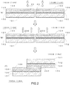
Fig. 2] Figs. 2A to 2C are cross-sectional views for illustrating a connecting step for connecting superconducting wires. - [
Fig. 3] Fig. 3A is a cross-sectional view showing a connection structure according to the present invention, andFig. 3B is a cross-sectional view showing a connection structure according to a comparative example. - [
Fig. 4] Figs. 4A and 4B are cross-sectional views for explaining a non-superconductor according to a variant embodiment. - [
Fig. 5] Fig. 5 is a cross-sectional view for explaining another application example according to the present embodiment. - A mode for carrying out the present invention (hereinafter referred to as the present embodiment) will be described with reference to an illustrative embodiment. The present embodiment relates to a connection structure of superconducting wires connecting a plurality of superconducting wires. First, prior to specific description on the connection structure of superconducting wires, the structure of a high-temperature superconducting wire will be described as an illustrative embodiment of the connection structure of superconducting wires with reference to cross-sectional views in
Figs. 1A and 1B . - As shown in
Fig. 1A , a high-temperaturesuperconducting wire 100 is one mode of a superconducting wire according to the present invention, and includes asubstrate 101, anintermediate layer 102, asuperconducting layer 103, and aprotection layer 104. - The
substrate 101 is formed to have a tape-like shape. For example, a low-magnetic non-oriented metal substrate or a non-oriented ceramic substrate is used as thesubstrate 101. As a material of the metal substrate, a metal such as Co, Cu, Ni, Ti, Mo, Nb, Ta, W, Mn, Fe, Ag or Cr, or an alloy thereof is used, which are excellent in strength and heat resistance. Stainless steels and nickel-based alloys represented by Hastelloy (registered trademark) which are excellent in corrosion resistance and heat resistance are particularly preferable. Further, for example, MgO, SrTiO3 or yttrium stabilized zirconia or the like is used as a material of the ceramic substrate. - The
intermediate layer 102 is an arbitrary layer serving as a base of thesuperconducting layer 103, and is a layer formed on thesubstrate 101 in order to achieve a high biaxial orientation property in thesuperconducting layer 103. For theintermediate layer 102, materials such as MgO and CeO2 are used in which values of physical characteristics such as a coefficient of thermal expansion and a lattice constant are intermediate values between thesubstrate 101 and a superconductor constituting thesuperconducting layer 103. Theintermediate layer 102 may have a monolayer structure or a multilayer structure. In a case where thesubstrate 101 is as metal substrate, theintermediate layer 102 may be a ceramic thin film. - The
superconducting layer 103 is formed on a surface of theintermediate layer 102, and with a superconductor as a main component, comprises at least one of elements among Cu, Ba, Y, Gd, Sm, Eu, Gd, Dy, Ho, Er, Tm, Yb, Lu, Zr and Hf. Specifically, a RE-based superconductor represented by REBa2Cu3O7-λ (λ represents an integer from 0 to 6) is used as the superconductor. RE in the RE-based superconductor contains a single rare earth element or a plurality of rare earth elements of Y, Nd, Sm, Eu, Gd, Dy, Ho, Er, Tm, Yb or Lu. - In order to connect
superconducting wires superconducting layer 103 as shown inFIG. 1B . - Specifically, as shown in
Fig. 1B , when thesuperconducting layer 103 is formed to have a multilayer structure by a chemical vapor deposition (CVD) method such that a film thickness per layer is less than 200 nm in a lower layer region 1031 which is from the lowermost layer to the sixth layer, and a film thickness of an uppermost layer 1032 (seventh layer) is greater than or equal to 200 nm, it is possible to cause the non-superconductor 105 (for example, copper oxide) to precipitate at the surface 103a of thesuperconducting layer 103 without affecting the superconducting characteristic of thesuperconducting layer 103. More specifically, the non-superconductor 105 can be formed such that a part of the non-superconductor 105 is embedded in thesuperconducting layer 103 while the remaining part of the non-superconductor 105 protrudes from the surface 103a of thesuperconducting layer 103. Further, an area density of the non-superconductors 105 on the surface 103a of thesuperconducting layer 103 can be checked or measured by observing the surface 103a of thesuperconducting layer 103 with an electron microscope or the like. - As described above, in the lamination step of the
superconducting layer 103 by the CVD method, by thickening the film thickness per layer to greater than or equal to 200 nm, copper oxide (CuxO) particles which are the non-superconductor 105 can be produced more easily. The non-superconductor 105 is not limited to copper oxide (CuxO) described above, but may be formed of at least one of elements among Cu, Ba, Al, Y, Gd, Sm, Eu, Gd, Dy, Ho, Er, Tm, Yb, Lu, Zr and Hf. - Furthermore, the non-superconductor 105 may be provided to protrude from the surface 103a of the
superconducting layer 103 by not only a CVD method, but also other methods such as a MOD method and a sol-gel method. - The
protection layer 104 is any layer covering the surface of thesuperconducting layer 103. For example, Ag or the like is used for theprotection layer 104. - Next, two
superconducting wires 100 each having the foregoing lamination structure are prepared, and a connecting step of connecting the preparedsuperconducting wires Figs. 2A to 2C . For convenience's sake, onesuperconducting wire 100 will be referred to as asuperconducting wire 100A, and theother superconducting wire 100 will be referred to as asuperconducting wire 100B. - First, as shown in
Fig. 2A , for each of thesuperconducting wire 100A and thesuperconducting wire 100B, theprotection layer 104 is etched only at a region necessary for connection to expose thesuperconducting layer 103. - Thereafter, a connecting
superconducting layer 200 is formed by a metal organic decomposition (MOD) method. Specifically, first, araw material solution 20 containing organic metal complex of Y, Ba, Cu or the like is prepared. The preparedraw material solution 20 is coated on a surface of the exposedsuperconducting layer 103. Here, theraw material solution 20 is coated over the entire surface of the exposedsuperconducting layer 103, but the coating amount is not specifically limited, and may be determined as appropriate. In the present embodiment, the method of coating theraw material solution 20 by the MOD method is presented, but the present embodiment is not limited thereto. - Subsequently, as shown in
Fig. 2B , each of thesuperconducting wire 100A and thesuperconducting wire 100B is subjected to calcination, so that organic solvent is vaporized from theraw material solution 20 coated on the surface of thesuperconducting layer 103. Here, calcination is performed by conducting a heat treatment at 400 to 600°C, for example. The organic metal complex contained in theraw material solution 20 is decomposed by calcination. By performing calcination as described above, the connectingsuperconducting layer 200 is formed over the entire surface of thesuperconducting layer 103 including a portion where the non-superconductor 105 is protruding. - Subsequently, as shown in
Fig. 2C , the connectingsuperconducting layers 200 which have been respectively formed on thesuperconducting layers 103 of thesuperconducting wires superconducting layers 200 are crystallized, whereby the connectingsuperconducting layers 200 are bonded to each other. Furthermore, as an oxygen anneal treatment, the temperature is decreased in an Ar atmosphere with an in oxygen concentration of greater than or equal to 50% to introduce oxygen into the connectingsuperconducting layers 200 which have been subjected to the firing treatment. This introduction of oxygen causes the connectingsuperconducting layers 200 to have a structure exhibiting the superconducting characteristic. -
Fig. 3A is an enlarged view showing the structure of a connecting region of thesuperconducting wires Fig. 3A , since each of thesuperconducting wires superconducting layer 103, the surfaces of the connectingsuperconducting layers 200 have irregularities. By overlapping thesuperconducting wires superconducting layers 200 having the uneven surfaces as described above oppose each other, agap 300 is formed at a joining portions of thesuperconducting wires superconducting layers gap 300 described above, oxygen is sufficiently supplied to the connectingsuperconducting layers superconducting layers - As described above, the
non-superconductors 105 protrude from the surface 103a of the superconducting layers 103. It is preferable that the protruding portions of thenon-superconductors 105 have an average diameter ranging from 0.1 to 10 µm and an average height ranging from 0.01 to 5 µm. The average diameter is obtained by observing with SEM to measure longest diameters and calculating an average value of the longest diameters. The average height can be measured by cutting the protruding portions in the thickness direction and observing cross-sections with SEM. When the average diameter and the average height are excessively large, there is a tendency that lots of voids are formed around the non-superconductors, and the connection strength decreases. When the average diameter and the average height are excessively small, the voids formed are small, and oxygen cannot be supplied sufficiently, so that a good superconducting characteristic cannot be obtained. - In comparison to the embodiment described above,
Fig. 3B is an enlarged view of the structure of a connecting region of superconducting wires 400A and 400B according to a comparative example. Each of the superconducting wires 400A and 400B according to the comparative example is obtained by polishing a non-superconductor 405 provided on a surface of asuperconducting layer 403 to flatten the surface of thesuperconducting layer 403. When the surfaces of thesuperconducting layers 403 are flat in this manner, the surfaces of connectingsuperconducting layers gap 300 as shown inFig. 3A is formed. As a result, the connectingsuperconducting layers - As is apparent from the result of comparison between the foregoing comparative example and the present embodiment, according to the connection structure of the
superconducting wires superconducting layers superconducting wires superconducting wires - The film thickness of the connecting
superconducting layer 200 ranges, when film formation is performed by a MOD method, preferably from 10 nm to 5 µm. This is because excessively small film thickness causes a decrease in the connection area between the connectingsuperconducting layers gap 300 cannot be formed and crystallization is made difficult. - According to the connection structure of the
superconducting wires voids 301 are formed, and thus it is preferable in that oxygen can be sufficiently supplied to the connectingsuperconducting layers 200 until crystallization is positively performed. - Furthermore, in the present embodiment, the non-superconductor 105 protrudes from the surfaces 103a of the
superconducting layers 103, and is also embedded in the surfaces 103a of thesuperconducting layers 103, so that the connection strength can be enhanced. Particularly, although existence of thevoids 301 described above causes reduction in connection strength, the present embodiment is preferable in that a strong connection structure can be achieved because thenon-superconductors 105 are embedded in the surfaces 103a of the superconducting layers 103. - The non-superconductor 105 of the present embodiment is not limited to those protruding from the surfaces 103a of the
superconducting layers 103 and embedded in the surfaces 103a of the superconducting layers 103. For example,Figs. 4A and 4B show a non-superconductor 105B according to a variant embodiment. That is, as shown inFig. 4A , on a surface of a superconducting layer 103B grown to have a flat surface, fine particles of alumina or the like may be provided as the non-superconductor 105B. Subsequently, as shown inFig. 4B , on the superconducting layer 103B provided with the non-superconductors 105B, a raw material solution is coated and subjected to calcination to form a connectingsuperconducting layer 200B having an uneven surface. Particularly, according to the variant embodiment shown inFigs. 4A and 4B , the uneven shape (the number of protrusions and recesses) of the surface 103a of thesuperconducting layer 103 can be easily adjusted by adjusting the density of the fine particles or the like without changing any of the conditions of the film formation of thesuperconducting layer 103. That is, the surface 103a of thesuperconducting layer 103 can be configured to have a surface shape suitable for crystallization of the connectingsuperconducting layer 200 by a simple method. - Further, in the present embodiment, as shown in
Figs. 2A to 2C andFigs. 3A and 3B , a case in which, in the connection structure in which the twosuperconducting wires superconducting layers 103 face each other, anon-superconducting layer 105 is provided at the overlapped portions at the surfaces of the superconducting layers has been illustrated. However, even in various connection structures, the superconducting wires can be connected to each other while achieving good superconducting characteristics. Here, "the overlapped portion at the surface of the superconducting layer" indicates a portion which will be afterwards joined to another superconducting layer and to be a joining portion. Specifically, it means a region of the surface of the superconducting layer which is exposed by etching and removing the protection layer. - For example, as shown in
Fig. 5 , as another application example, a connection structure is illustrated in which first and secondsuperconducting wires third superconducting wire 100E, with the first and secondsuperconducting wires superconducting wires superconducting wires third superconducting wire 100E is arranged to oppose the surfaces of the superconducting layers of the first and secondsuperconducting wires superconducting wires superconducting layer 103 of each of the first to thirdsuperconducting wires superconducting wires - In an application example other than the application example shown in
Fig. 5 , it is possible to achieve a substantially Y-shaped branched connection structure, for example, by dividing a termination region of one superconducting wire into two regions and making two different superconducting wires come face to face with each other in each of the regions. - In the present embodiment, the non-superconductors are provided on the surfaces of the superconducting layers of all the superconducting wires to be connected. However, the present invention is not limited to such an embodiment. For example, non-superconductors may be provided on only one superconducting layer of two superconducting layers facing each other. When the surface of the connecting superconducting layer of one superconducting wire has irregularities, a gap is formed between the connecting superconducting layers, and the connecting superconducting layers can be positively crystallized. Furthermore, as shown in
Fig. 2C , when parts of the superconducting layers are connected with each other, it is not necessary to provide the non-superconductors on the entire surfaces of the superconducting layers, and the non-superconductors may be provided on at least the overlap portions of the surfaces of the superconducting layers. -
- 100, 100A, 100B, 100C, 100D, 100E superconducting wire
- 101 substrate
- 102 intermediate layer
- 103 superconducting layer
- 103a surface
- 104 protection layer
- 105 non-superconductor
- 300 gap
- 301 void
Claims (8)
- A connection structure of superconducting wires in which a plurality of superconducting wires are overlapped and connected with each other, each of the plurality of superconducting wires including a substrate and a superconducting layer that are laminated, characterized in that a non-superconductor is provided at a part of a surface of the superconducting layer of at least one of the superconducting wires and protrudes from the surface.
- The connection structure of superconducting wires according to claim 1, characterized in that a part of the non-superconductor is embedded in the surface of the superconducting layer.
- The connection structure of superconducting wires according to claim 1 or 2, characterized in that an intermediate layer is provided between the substrate and the superconducting layer.
- The connection structure of superconducting wires according to any one of claims 1 to 3, characterized in that a connecting superconducting layer constituting a joining portion with another superconducting wire is formed on the surface of the superconducting layer including a protruding portion of the non-superconductor.
- The connection structure of superconducting wires according to any one of claims 1 to 4, characterized in that the non-superconductor contains at least one element among Cu, Ba, Al, Y, Gd, Sm, Eu, Gd, Dy, Ho, Er, Tm, Yb, Lu, Zr and Hf.
- The connection structure of superconducting wires according to any one of claims 1 to 5, characterized in that the non-superconductor includes CuOx.
- The connection structure of superconducting wires according to any one of claims 1 to 6, characterized in that the plurality of superconducting wires are two superconducting wires, and the non-superconductor is provided on an overlap portion which is to be a joining portion on the surface of the superconducting layer of at least one superconducting wire.
- The connection structure of superconducting wires according to any one of claims 1 to 6, characterized in that
the plurality of superconducting wires are three superconducting wires, and,
in a connection structure in which first and second superconducting wires are overlapped with and connected to a third superconducting wire, with the first and second superconducting wires being in a positional relationship in which the surfaces of the superconducting layers of the first and second superconducting wires are in the same direction with end faces of the first and second superconducting wires facing each other, and the third superconducting wire is arranged to oppose the surfaces of the superconducting layers of the first and second superconducting wires in a positional relationship in which the third superconducting wire extends across and is connected to both surfaces of the superconducting layers of the first and second superconducting wires, and
the non-superconductor is provided at an overlap portion which is to be a joining portion on a surface of the superconducting layer of at least one of the opposing superconducting wires.
Applications Claiming Priority (2)
| Application Number | Priority Date | Filing Date | Title |
|---|---|---|---|
| JP2015195751 | 2015-10-01 | ||
| PCT/JP2016/078664 WO2017057483A1 (en) | 2015-10-01 | 2016-09-28 | Connection structure for superconductive wire rod |
Publications (2)
| Publication Number | Publication Date |
|---|---|
| EP3358576A1 true EP3358576A1 (en) | 2018-08-08 |
| EP3358576A4 EP3358576A4 (en) | 2019-05-15 |
Family
ID=58423732
Family Applications (1)
| Application Number | Title | Priority Date | Filing Date |
|---|---|---|---|
| EP16851654.0A Withdrawn EP3358576A4 (en) | 2015-10-01 | 2016-09-28 | Connection structure for superconductive wire rod |
Country Status (5)
| Country | Link |
|---|---|
| US (1) | US10541068B2 (en) |
| EP (1) | EP3358576A4 (en) |
| JP (1) | JP6667543B2 (en) |
| CN (1) | CN108028106B (en) |
| WO (1) | WO2017057483A1 (en) |
Families Citing this family (6)
| Publication number | Priority date | Publication date | Assignee | Title |
|---|---|---|---|---|
| DE102015219956A1 (en) * | 2015-10-14 | 2017-04-20 | Bruker Hts Gmbh | Superconductor structure for connecting strip conductors, in particular with a wavy or serrated seam |
| JP2018142409A (en) * | 2017-02-27 | 2018-09-13 | 古河電気工業株式会社 | Superconducting wire connection structure |
| US12119137B2 (en) | 2019-12-05 | 2024-10-15 | Furukawa Electric Co., Ltd. | Connection structure of high temperature superconducting wires, method for forming same, high temperature superconducting wire, and high temperature superconducting coil |
| CN113594348B (en) * | 2020-04-30 | 2024-10-29 | 中国科学院电工研究所 | Composite superconducting wire and its preparation method and connection method, and a connecting superconducting wire |
| JP7481963B2 (en) * | 2020-09-01 | 2024-05-13 | 株式会社東芝 | Superconducting layer connection structure, superconducting wire, superconducting coil, superconducting device, and superconducting layer connection method |
| JP7472067B2 (en) * | 2021-03-19 | 2024-04-22 | 株式会社東芝 | Superconducting layer connection structure, superconducting wire, superconducting coil, and superconducting device |
Family Cites Families (15)
| Publication number | Priority date | Publication date | Assignee | Title |
|---|---|---|---|---|
| US5079222A (en) | 1987-08-31 | 1992-01-07 | Semiconductor Energy Laboratory Co., Ltd. | Superconducting ceramic circuits and manufacturing method for the same |
| US5225394A (en) | 1987-08-31 | 1993-07-06 | Semiconductor Energy Laboratory Co., Ltd. | Method for manufacturing high Tc superconducting circuits |
| US5786304A (en) * | 1992-04-03 | 1998-07-28 | Nippon Steel Corporation | Joining product of oxide superconducting material and process for producing the same |
| JPH0645046A (en) * | 1992-07-23 | 1994-02-18 | Sumitomo Heavy Ind Ltd | Method for forming electrode in oxide superconductor |
| US6159905A (en) * | 1999-06-02 | 2000-12-12 | Buzcek; David M. | Methods for joining high temperature superconducting components with negligible critical current degradation and articles of manufacture in accordance therewith |
| WO2010016720A2 (en) * | 2008-08-04 | 2010-02-11 | 고려대학교 산학협력단 | Melting diffusion welding method for second generation high temperature superconducting wire |
| JP5686437B2 (en) * | 2011-04-27 | 2015-03-18 | 住友電気工業株式会社 | Oxide superconducting thin film wire and method for producing the same |
| US9502159B2 (en) * | 2012-05-02 | 2016-11-22 | Furukawa Electric Co., Ltd. | Superconducting wire connection structure, superconducting wire connection method, and connection superconducting wire |
| JP5828299B2 (en) | 2012-05-08 | 2015-12-02 | 住友電気工業株式会社 | High temperature superconducting thin film wire joining method and high temperature superconducting thin film wire |
| KR101374177B1 (en) * | 2012-10-11 | 2014-03-14 | 케이조인스(주) | Methods of splicing 2g rebco high temperature superconductors using partial micro-melting diffusion pressurized splicing by direct face-to-face contact of high temperature superconducting layers and recovering superconductivity by oxygenation annealing |
| US9362026B2 (en) * | 2013-01-09 | 2016-06-07 | Fujikura Ltd. | Oxide superconductor wire, connection structure thereof, and superconductor equipment |
| WO2014116289A1 (en) | 2013-01-22 | 2014-07-31 | Champagne Wesley Jon | Hoof mounting for farrier training system |
| JP6210537B2 (en) * | 2013-08-06 | 2017-10-11 | 古河電気工業株式会社 | Superconducting cable connection structure, superconducting cable, current terminal structure at the end of superconducting cable |
| US9947441B2 (en) * | 2013-11-12 | 2018-04-17 | Varian Semiconductor Equipment Associates, Inc. | Integrated superconductor device and method of fabrication |
| JP6419596B2 (en) * | 2015-02-13 | 2018-11-07 | 株式会社東芝 | Thin-film wire connection structure, high-temperature superconducting wire using the connection structure, and high-temperature superconducting coil using the connection structure |
-
2016
- 2016-09-28 CN CN201680056181.7A patent/CN108028106B/en active Active
- 2016-09-28 EP EP16851654.0A patent/EP3358576A4/en not_active Withdrawn
- 2016-09-28 WO PCT/JP2016/078664 patent/WO2017057483A1/en not_active Ceased
- 2016-09-28 JP JP2017543503A patent/JP6667543B2/en active Active
-
2018
- 2018-03-29 US US15/940,358 patent/US10541068B2/en active Active
Also Published As
| Publication number | Publication date |
|---|---|
| EP3358576A4 (en) | 2019-05-15 |
| JPWO2017057483A1 (en) | 2018-07-19 |
| CN108028106A (en) | 2018-05-11 |
| US20180218809A1 (en) | 2018-08-02 |
| US10541068B2 (en) | 2020-01-21 |
| CN108028106B (en) | 2020-03-06 |
| WO2017057483A1 (en) | 2017-04-06 |
| JP6667543B2 (en) | 2020-03-18 |
Similar Documents
| Publication | Publication Date | Title |
|---|---|---|
| US10541068B2 (en) | Connection structure of superconducting wires | |
| JP5806302B2 (en) | Multifilament superconductor with reduced AC loss and its formation method | |
| EP1925040B1 (en) | High temperature superconducting wires and coils | |
| EP2801983B1 (en) | Superconducting wire and superconducting coil | |
| US8993485B2 (en) | Methods of splicing 2G rebco high temperature superconductors using partial micro-melting diffusion pressurized splicing by direct face-to-face contact of high temperature superconducting layers and recovering superconductivity by oxygenation annealing | |
| US20200028061A1 (en) | Connection structure | |
| US7463915B2 (en) | Stacked filamentary coated superconductors | |
| WO2001008169A9 (en) | Superconductor coated conductors with reduced a.c. loss | |
| Huang et al. | An efficient approach for superconducting joint of YBCO coated conductors | |
| US11488746B2 (en) | Superconductor with improved flux pinning at low temperatures | |
| CN102870244B (en) | The formation of thick oxide films of single coating | |
| KR101289999B1 (en) | Process for producing superconducting thin-film material and superconducting equipment | |
| US8470744B2 (en) | High temperature superconductor, in particular improved coated conductor | |
| JP6605942B2 (en) | Superconducting wire connection structure and superconducting wire connection method | |
| JP5416924B2 (en) | Superconducting wire and method for manufacturing the same | |
| KR20210026613A (en) | High temperature superconducting wire with multi-superconducting layer | |
| EP2284917A1 (en) | Coated conductor | |
| JP2012064495A (en) | Method of producing coated superconducting wire rod, electrodeposition method of superconducting wire rod, and coated superconducting wire rod | |
| EP2372722B1 (en) | Method for manufacturing precursor, method for manufacturing superconducting wire, precursor, and superconducting wire | |
| US7781377B2 (en) | Anti-epitaxial film in a superconducting article and related articles, devices and systems | |
| JP2006107843A (en) | Tape-shaped superconducting wire | |
| JP2017147189A (en) | Oxide superconducting wire and method for producing oxide superconducting wire |
Legal Events
| Date | Code | Title | Description |
|---|---|---|---|
| STAA | Information on the status of an ep patent application or granted ep patent |
Free format text: STATUS: THE INTERNATIONAL PUBLICATION HAS BEEN MADE |
|
| PUAI | Public reference made under article 153(3) epc to a published international application that has entered the european phase |
Free format text: ORIGINAL CODE: 0009012 |
|
| STAA | Information on the status of an ep patent application or granted ep patent |
Free format text: STATUS: REQUEST FOR EXAMINATION WAS MADE |
|
| 17P | Request for examination filed |
Effective date: 20180320 |
|
| AK | Designated contracting states |
Kind code of ref document: A1 Designated state(s): AL AT BE BG CH CY CZ DE DK EE ES FI FR GB GR HR HU IE IS IT LI LT LU LV MC MK MT NL NO PL PT RO RS SE SI SK SM TR |
|
| AX | Request for extension of the european patent |
Extension state: BA ME |
|
| DAV | Request for validation of the european patent (deleted) | ||
| DAX | Request for extension of the european patent (deleted) | ||
| A4 | Supplementary search report drawn up and despatched |
Effective date: 20190416 |
|
| RIC1 | Information provided on ipc code assigned before grant |
Ipc: H01B 12/06 20060101ALI20190410BHEP Ipc: H01L 39/02 20060101AFI20190410BHEP Ipc: H01F 6/06 20060101ALI20190410BHEP |
|
| STAA | Information on the status of an ep patent application or granted ep patent |
Free format text: STATUS: EXAMINATION IS IN PROGRESS |
|
| 17Q | First examination report despatched |
Effective date: 20191119 |
|
| STAA | Information on the status of an ep patent application or granted ep patent |
Free format text: STATUS: THE APPLICATION IS DEEMED TO BE WITHDRAWN |
|
| 18D | Application deemed to be withdrawn |
Effective date: 20200603 |