EP3358400A1 - Light-modulating cell - Google Patents
Light-modulating cell Download PDFInfo
- Publication number
- EP3358400A1 EP3358400A1 EP16851790.2A EP16851790A EP3358400A1 EP 3358400 A1 EP3358400 A1 EP 3358400A1 EP 16851790 A EP16851790 A EP 16851790A EP 3358400 A1 EP3358400 A1 EP 3358400A1
- Authority
- EP
- European Patent Office
- Prior art keywords
- light
- spacers
- pair
- liquid crystal
- modulating cell
- Prior art date
- Legal status (The legal status is an assumption and is not a legal conclusion. Google has not performed a legal analysis and makes no representation as to the accuracy of the status listed.)
- Granted
Links
- 125000006850 spacer group Chemical group 0.000 claims abstract description 262
- 239000004973 liquid crystal related substance Substances 0.000 claims description 152
- 239000000758 substrate Substances 0.000 claims description 48
- 239000000049 pigment Substances 0.000 claims description 33
- 239000011347 resin Substances 0.000 claims description 8
- 229920005989 resin Polymers 0.000 claims description 8
- 239000010408 film Substances 0.000 description 192
- 210000004027 cell Anatomy 0.000 description 104
- 238000000034 method Methods 0.000 description 25
- 230000008859 change Effects 0.000 description 16
- 230000005684 electric field Effects 0.000 description 16
- 230000005540 biological transmission Effects 0.000 description 10
- 230000010287 polarization Effects 0.000 description 10
- 238000010521 absorption reaction Methods 0.000 description 9
- 238000000206 photolithography Methods 0.000 description 9
- 210000002858 crystal cell Anatomy 0.000 description 7
- 238000002834 transmittance Methods 0.000 description 7
- 239000000463 material Substances 0.000 description 5
- 230000001276 controlling effect Effects 0.000 description 4
- 230000000694 effects Effects 0.000 description 4
- 239000011521 glass Substances 0.000 description 4
- 238000010586 diagram Methods 0.000 description 3
- 230000003287 optical effect Effects 0.000 description 3
- 230000008569 process Effects 0.000 description 3
- 230000000052 comparative effect Effects 0.000 description 2
- 239000000975 dye Substances 0.000 description 2
- 238000004519 manufacturing process Methods 0.000 description 2
- 238000005259 measurement Methods 0.000 description 2
- 238000012986 modification Methods 0.000 description 2
- 230000004048 modification Effects 0.000 description 2
- 230000001105 regulatory effect Effects 0.000 description 2
- 239000010409 thin film Substances 0.000 description 2
- 239000004677 Nylon Substances 0.000 description 1
- 239000004642 Polyimide Substances 0.000 description 1
- 238000007792 addition Methods 0.000 description 1
- 239000011248 coating agent Substances 0.000 description 1
- 238000000576 coating method Methods 0.000 description 1
- 238000004040 coloring Methods 0.000 description 1
- 238000012217 deletion Methods 0.000 description 1
- 230000037430 deletion Effects 0.000 description 1
- 238000013461 design Methods 0.000 description 1
- AMGQUBHHOARCQH-UHFFFAOYSA-N indium;oxotin Chemical compound [In].[Sn]=O AMGQUBHHOARCQH-UHFFFAOYSA-N 0.000 description 1
- 229920001778 nylon Polymers 0.000 description 1
- 238000000016 photochemical curing Methods 0.000 description 1
- 239000004417 polycarbonate Substances 0.000 description 1
- 229920000515 polycarbonate Polymers 0.000 description 1
- 229920001721 polyimide Polymers 0.000 description 1
- 230000009467 reduction Effects 0.000 description 1
- 238000011160 research Methods 0.000 description 1
- 239000012780 transparent material Substances 0.000 description 1
Images


Classifications
-
- G—PHYSICS
- G02—OPTICS
- G02F—OPTICAL DEVICES OR ARRANGEMENTS FOR THE CONTROL OF LIGHT BY MODIFICATION OF THE OPTICAL PROPERTIES OF THE MEDIA OF THE ELEMENTS INVOLVED THEREIN; NON-LINEAR OPTICS; FREQUENCY-CHANGING OF LIGHT; OPTICAL LOGIC ELEMENTS; OPTICAL ANALOGUE/DIGITAL CONVERTERS
- G02F1/00—Devices or arrangements for the control of the intensity, colour, phase, polarisation or direction of light arriving from an independent light source, e.g. switching, gating or modulating; Non-linear optics
- G02F1/01—Devices or arrangements for the control of the intensity, colour, phase, polarisation or direction of light arriving from an independent light source, e.g. switching, gating or modulating; Non-linear optics for the control of the intensity, phase, polarisation or colour
- G02F1/13—Devices or arrangements for the control of the intensity, colour, phase, polarisation or direction of light arriving from an independent light source, e.g. switching, gating or modulating; Non-linear optics for the control of the intensity, phase, polarisation or colour based on liquid crystals, e.g. single liquid crystal display cells
- G02F1/133—Constructional arrangements; Operation of liquid crystal cells; Circuit arrangements
- G02F1/1333—Constructional arrangements; Manufacturing methods
- G02F1/1339—Gaskets; Spacers; Sealing of cells
- G02F1/13394—Gaskets; Spacers; Sealing of cells spacers regularly patterned on the cell subtrate, e.g. walls, pillars
-
- C—CHEMISTRY; METALLURGY
- C09—DYES; PAINTS; POLISHES; NATURAL RESINS; ADHESIVES; COMPOSITIONS NOT OTHERWISE PROVIDED FOR; APPLICATIONS OF MATERIALS NOT OTHERWISE PROVIDED FOR
- C09K—MATERIALS FOR MISCELLANEOUS APPLICATIONS, NOT PROVIDED FOR ELSEWHERE
- C09K19/00—Liquid crystal materials
- C09K19/52—Liquid crystal materials characterised by components which are not liquid crystals, e.g. additives with special physical aspect: solvents, solid particles
- C09K19/60—Pleochroic dyes
-
- E—FIXED CONSTRUCTIONS
- E06—DOORS, WINDOWS, SHUTTERS, OR ROLLER BLINDS IN GENERAL; LADDERS
- E06B—FIXED OR MOVABLE CLOSURES FOR OPENINGS IN BUILDINGS, VEHICLES, FENCES OR LIKE ENCLOSURES IN GENERAL, e.g. DOORS, WINDOWS, BLINDS, GATES
- E06B3/00—Window sashes, door leaves, or like elements for closing wall or like openings; Layout of fixed or moving closures, e.g. windows in wall or like openings; Features of rigidly-mounted outer frames relating to the mounting of wing frames
- E06B3/66—Units comprising two or more parallel glass or like panes permanently secured together
- E06B3/663—Elements for spacing panes
- E06B3/66304—Discrete spacing elements, e.g. for evacuated glazing units
-
- E—FIXED CONSTRUCTIONS
- E06—DOORS, WINDOWS, SHUTTERS, OR ROLLER BLINDS IN GENERAL; LADDERS
- E06B—FIXED OR MOVABLE CLOSURES FOR OPENINGS IN BUILDINGS, VEHICLES, FENCES OR LIKE ENCLOSURES IN GENERAL, e.g. DOORS, WINDOWS, BLINDS, GATES
- E06B3/00—Window sashes, door leaves, or like elements for closing wall or like openings; Layout of fixed or moving closures, e.g. windows in wall or like openings; Features of rigidly-mounted outer frames relating to the mounting of wing frames
- E06B3/66—Units comprising two or more parallel glass or like panes permanently secured together
- E06B3/67—Units comprising two or more parallel glass or like panes permanently secured together characterised by additional arrangements or devices for heat or sound insulation or for controlled passage of light
- E06B3/6715—Units comprising two or more parallel glass or like panes permanently secured together characterised by additional arrangements or devices for heat or sound insulation or for controlled passage of light specially adapted for increased thermal insulation or for controlled passage of light
- E06B3/6722—Units comprising two or more parallel glass or like panes permanently secured together characterised by additional arrangements or devices for heat or sound insulation or for controlled passage of light specially adapted for increased thermal insulation or for controlled passage of light with adjustable passage of light
-
- G—PHYSICS
- G02—OPTICS
- G02F—OPTICAL DEVICES OR ARRANGEMENTS FOR THE CONTROL OF LIGHT BY MODIFICATION OF THE OPTICAL PROPERTIES OF THE MEDIA OF THE ELEMENTS INVOLVED THEREIN; NON-LINEAR OPTICS; FREQUENCY-CHANGING OF LIGHT; OPTICAL LOGIC ELEMENTS; OPTICAL ANALOGUE/DIGITAL CONVERTERS
- G02F1/00—Devices or arrangements for the control of the intensity, colour, phase, polarisation or direction of light arriving from an independent light source, e.g. switching, gating or modulating; Non-linear optics
- G02F1/01—Devices or arrangements for the control of the intensity, colour, phase, polarisation or direction of light arriving from an independent light source, e.g. switching, gating or modulating; Non-linear optics for the control of the intensity, phase, polarisation or colour
- G02F1/13—Devices or arrangements for the control of the intensity, colour, phase, polarisation or direction of light arriving from an independent light source, e.g. switching, gating or modulating; Non-linear optics for the control of the intensity, phase, polarisation or colour based on liquid crystals, e.g. single liquid crystal display cells
- G02F1/133—Constructional arrangements; Operation of liquid crystal cells; Circuit arrangements
- G02F1/13306—Circuit arrangements or driving methods for the control of single liquid crystal cells
- G02F1/13318—Circuits comprising a photodetector
-
- G—PHYSICS
- G02—OPTICS
- G02F—OPTICAL DEVICES OR ARRANGEMENTS FOR THE CONTROL OF LIGHT BY MODIFICATION OF THE OPTICAL PROPERTIES OF THE MEDIA OF THE ELEMENTS INVOLVED THEREIN; NON-LINEAR OPTICS; FREQUENCY-CHANGING OF LIGHT; OPTICAL LOGIC ELEMENTS; OPTICAL ANALOGUE/DIGITAL CONVERTERS
- G02F1/00—Devices or arrangements for the control of the intensity, colour, phase, polarisation or direction of light arriving from an independent light source, e.g. switching, gating or modulating; Non-linear optics
- G02F1/01—Devices or arrangements for the control of the intensity, colour, phase, polarisation or direction of light arriving from an independent light source, e.g. switching, gating or modulating; Non-linear optics for the control of the intensity, phase, polarisation or colour
- G02F1/13—Devices or arrangements for the control of the intensity, colour, phase, polarisation or direction of light arriving from an independent light source, e.g. switching, gating or modulating; Non-linear optics for the control of the intensity, phase, polarisation or colour based on liquid crystals, e.g. single liquid crystal display cells
- G02F1/133—Constructional arrangements; Operation of liquid crystal cells; Circuit arrangements
- G02F1/1333—Constructional arrangements; Manufacturing methods
- G02F1/1335—Structural association of cells with optical devices, e.g. polarisers or reflectors
- G02F1/133528—Polarisers
-
- G—PHYSICS
- G02—OPTICS
- G02F—OPTICAL DEVICES OR ARRANGEMENTS FOR THE CONTROL OF LIGHT BY MODIFICATION OF THE OPTICAL PROPERTIES OF THE MEDIA OF THE ELEMENTS INVOLVED THEREIN; NON-LINEAR OPTICS; FREQUENCY-CHANGING OF LIGHT; OPTICAL LOGIC ELEMENTS; OPTICAL ANALOGUE/DIGITAL CONVERTERS
- G02F1/00—Devices or arrangements for the control of the intensity, colour, phase, polarisation or direction of light arriving from an independent light source, e.g. switching, gating or modulating; Non-linear optics
- G02F1/01—Devices or arrangements for the control of the intensity, colour, phase, polarisation or direction of light arriving from an independent light source, e.g. switching, gating or modulating; Non-linear optics for the control of the intensity, phase, polarisation or colour
- G02F1/13—Devices or arrangements for the control of the intensity, colour, phase, polarisation or direction of light arriving from an independent light source, e.g. switching, gating or modulating; Non-linear optics for the control of the intensity, phase, polarisation or colour based on liquid crystals, e.g. single liquid crystal display cells
- G02F1/133—Constructional arrangements; Operation of liquid crystal cells; Circuit arrangements
- G02F1/1333—Constructional arrangements; Manufacturing methods
- G02F1/1337—Surface-induced orientation of the liquid crystal molecules, e.g. by alignment layers
- G02F1/133707—Structures for producing distorted electric fields, e.g. bumps, protrusions, recesses, slits in pixel electrodes
-
- G—PHYSICS
- G02—OPTICS
- G02F—OPTICAL DEVICES OR ARRANGEMENTS FOR THE CONTROL OF LIGHT BY MODIFICATION OF THE OPTICAL PROPERTIES OF THE MEDIA OF THE ELEMENTS INVOLVED THEREIN; NON-LINEAR OPTICS; FREQUENCY-CHANGING OF LIGHT; OPTICAL LOGIC ELEMENTS; OPTICAL ANALOGUE/DIGITAL CONVERTERS
- G02F1/00—Devices or arrangements for the control of the intensity, colour, phase, polarisation or direction of light arriving from an independent light source, e.g. switching, gating or modulating; Non-linear optics
- G02F1/01—Devices or arrangements for the control of the intensity, colour, phase, polarisation or direction of light arriving from an independent light source, e.g. switching, gating or modulating; Non-linear optics for the control of the intensity, phase, polarisation or colour
- G02F1/13—Devices or arrangements for the control of the intensity, colour, phase, polarisation or direction of light arriving from an independent light source, e.g. switching, gating or modulating; Non-linear optics for the control of the intensity, phase, polarisation or colour based on liquid crystals, e.g. single liquid crystal display cells
- G02F1/133—Constructional arrangements; Operation of liquid crystal cells; Circuit arrangements
- G02F1/1333—Constructional arrangements; Manufacturing methods
- G02F1/1339—Gaskets; Spacers; Sealing of cells
- G02F1/13392—Gaskets; Spacers; Sealing of cells spacers dispersed on the cell substrate, e.g. spherical particles, microfibres
-
- G—PHYSICS
- G02—OPTICS
- G02F—OPTICAL DEVICES OR ARRANGEMENTS FOR THE CONTROL OF LIGHT BY MODIFICATION OF THE OPTICAL PROPERTIES OF THE MEDIA OF THE ELEMENTS INVOLVED THEREIN; NON-LINEAR OPTICS; FREQUENCY-CHANGING OF LIGHT; OPTICAL LOGIC ELEMENTS; OPTICAL ANALOGUE/DIGITAL CONVERTERS
- G02F1/00—Devices or arrangements for the control of the intensity, colour, phase, polarisation or direction of light arriving from an independent light source, e.g. switching, gating or modulating; Non-linear optics
- G02F1/01—Devices or arrangements for the control of the intensity, colour, phase, polarisation or direction of light arriving from an independent light source, e.g. switching, gating or modulating; Non-linear optics for the control of the intensity, phase, polarisation or colour
- G02F1/13—Devices or arrangements for the control of the intensity, colour, phase, polarisation or direction of light arriving from an independent light source, e.g. switching, gating or modulating; Non-linear optics for the control of the intensity, phase, polarisation or colour based on liquid crystals, e.g. single liquid crystal display cells
- G02F1/133—Constructional arrangements; Operation of liquid crystal cells; Circuit arrangements
- G02F1/1333—Constructional arrangements; Manufacturing methods
- G02F1/1343—Electrodes
- G02F1/134309—Electrodes characterised by their geometrical arrangement
-
- G—PHYSICS
- G02—OPTICS
- G02F—OPTICAL DEVICES OR ARRANGEMENTS FOR THE CONTROL OF LIGHT BY MODIFICATION OF THE OPTICAL PROPERTIES OF THE MEDIA OF THE ELEMENTS INVOLVED THEREIN; NON-LINEAR OPTICS; FREQUENCY-CHANGING OF LIGHT; OPTICAL LOGIC ELEMENTS; OPTICAL ANALOGUE/DIGITAL CONVERTERS
- G02F1/00—Devices or arrangements for the control of the intensity, colour, phase, polarisation or direction of light arriving from an independent light source, e.g. switching, gating or modulating; Non-linear optics
- G02F1/01—Devices or arrangements for the control of the intensity, colour, phase, polarisation or direction of light arriving from an independent light source, e.g. switching, gating or modulating; Non-linear optics for the control of the intensity, phase, polarisation or colour
- G02F1/13—Devices or arrangements for the control of the intensity, colour, phase, polarisation or direction of light arriving from an independent light source, e.g. switching, gating or modulating; Non-linear optics for the control of the intensity, phase, polarisation or colour based on liquid crystals, e.g. single liquid crystal display cells
- G02F1/137—Devices or arrangements for the control of the intensity, colour, phase, polarisation or direction of light arriving from an independent light source, e.g. switching, gating or modulating; Non-linear optics for the control of the intensity, phase, polarisation or colour based on liquid crystals, e.g. single liquid crystal display cells characterised by the electro-optical or magneto-optical effect, e.g. field-induced phase transition, orientation effect, guest-host interaction or dynamic scattering
- G02F1/13725—Devices or arrangements for the control of the intensity, colour, phase, polarisation or direction of light arriving from an independent light source, e.g. switching, gating or modulating; Non-linear optics for the control of the intensity, phase, polarisation or colour based on liquid crystals, e.g. single liquid crystal display cells characterised by the electro-optical or magneto-optical effect, e.g. field-induced phase transition, orientation effect, guest-host interaction or dynamic scattering based on guest-host interaction
-
- E—FIXED CONSTRUCTIONS
- E06—DOORS, WINDOWS, SHUTTERS, OR ROLLER BLINDS IN GENERAL; LADDERS
- E06B—FIXED OR MOVABLE CLOSURES FOR OPENINGS IN BUILDINGS, VEHICLES, FENCES OR LIKE ENCLOSURES IN GENERAL, e.g. DOORS, WINDOWS, BLINDS, GATES
- E06B9/00—Screening or protective devices for wall or similar openings, with or without operating or securing mechanisms; Closures of similar construction
- E06B9/24—Screens or other constructions affording protection against light, especially against sunshine; Similar screens for privacy or appearance; Slat blinds
- E06B2009/2417—Light path control; means to control reflection
-
- E—FIXED CONSTRUCTIONS
- E06—DOORS, WINDOWS, SHUTTERS, OR ROLLER BLINDS IN GENERAL; LADDERS
- E06B—FIXED OR MOVABLE CLOSURES FOR OPENINGS IN BUILDINGS, VEHICLES, FENCES OR LIKE ENCLOSURES IN GENERAL, e.g. DOORS, WINDOWS, BLINDS, GATES
- E06B9/00—Screening or protective devices for wall or similar openings, with or without operating or securing mechanisms; Closures of similar construction
- E06B9/24—Screens or other constructions affording protection against light, especially against sunshine; Similar screens for privacy or appearance; Slat blinds
- E06B2009/2464—Screens or other constructions affording protection against light, especially against sunshine; Similar screens for privacy or appearance; Slat blinds featuring transparency control by applying voltage, e.g. LCD, electrochromic panels
-
- G—PHYSICS
- G02—OPTICS
- G02F—OPTICAL DEVICES OR ARRANGEMENTS FOR THE CONTROL OF LIGHT BY MODIFICATION OF THE OPTICAL PROPERTIES OF THE MEDIA OF THE ELEMENTS INVOLVED THEREIN; NON-LINEAR OPTICS; FREQUENCY-CHANGING OF LIGHT; OPTICAL LOGIC ELEMENTS; OPTICAL ANALOGUE/DIGITAL CONVERTERS
- G02F1/00—Devices or arrangements for the control of the intensity, colour, phase, polarisation or direction of light arriving from an independent light source, e.g. switching, gating or modulating; Non-linear optics
- G02F1/01—Devices or arrangements for the control of the intensity, colour, phase, polarisation or direction of light arriving from an independent light source, e.g. switching, gating or modulating; Non-linear optics for the control of the intensity, phase, polarisation or colour
- G02F1/13—Devices or arrangements for the control of the intensity, colour, phase, polarisation or direction of light arriving from an independent light source, e.g. switching, gating or modulating; Non-linear optics for the control of the intensity, phase, polarisation or colour based on liquid crystals, e.g. single liquid crystal display cells
- G02F1/133—Constructional arrangements; Operation of liquid crystal cells; Circuit arrangements
- G02F1/13306—Circuit arrangements or driving methods for the control of single liquid crystal cells
- G02F1/13312—Circuits comprising photodetectors for purposes other than feedback
-
- G—PHYSICS
- G02—OPTICS
- G02F—OPTICAL DEVICES OR ARRANGEMENTS FOR THE CONTROL OF LIGHT BY MODIFICATION OF THE OPTICAL PROPERTIES OF THE MEDIA OF THE ELEMENTS INVOLVED THEREIN; NON-LINEAR OPTICS; FREQUENCY-CHANGING OF LIGHT; OPTICAL LOGIC ELEMENTS; OPTICAL ANALOGUE/DIGITAL CONVERTERS
- G02F1/00—Devices or arrangements for the control of the intensity, colour, phase, polarisation or direction of light arriving from an independent light source, e.g. switching, gating or modulating; Non-linear optics
- G02F1/01—Devices or arrangements for the control of the intensity, colour, phase, polarisation or direction of light arriving from an independent light source, e.g. switching, gating or modulating; Non-linear optics for the control of the intensity, phase, polarisation or colour
- G02F1/13—Devices or arrangements for the control of the intensity, colour, phase, polarisation or direction of light arriving from an independent light source, e.g. switching, gating or modulating; Non-linear optics for the control of the intensity, phase, polarisation or colour based on liquid crystals, e.g. single liquid crystal display cells
- G02F1/133—Constructional arrangements; Operation of liquid crystal cells; Circuit arrangements
- G02F1/1333—Constructional arrangements; Manufacturing methods
- G02F1/1339—Gaskets; Spacers; Sealing of cells
- G02F1/13398—Spacer materials; Spacer properties
-
- G—PHYSICS
- G02—OPTICS
- G02F—OPTICAL DEVICES OR ARRANGEMENTS FOR THE CONTROL OF LIGHT BY MODIFICATION OF THE OPTICAL PROPERTIES OF THE MEDIA OF THE ELEMENTS INVOLVED THEREIN; NON-LINEAR OPTICS; FREQUENCY-CHANGING OF LIGHT; OPTICAL LOGIC ELEMENTS; OPTICAL ANALOGUE/DIGITAL CONVERTERS
- G02F2201/00—Constructional arrangements not provided for in groups G02F1/00 - G02F7/00
- G02F2201/08—Constructional arrangements not provided for in groups G02F1/00 - G02F7/00 light absorbing layer
-
- G—PHYSICS
- G02—OPTICS
- G02F—OPTICAL DEVICES OR ARRANGEMENTS FOR THE CONTROL OF LIGHT BY MODIFICATION OF THE OPTICAL PROPERTIES OF THE MEDIA OF THE ELEMENTS INVOLVED THEREIN; NON-LINEAR OPTICS; FREQUENCY-CHANGING OF LIGHT; OPTICAL LOGIC ELEMENTS; OPTICAL ANALOGUE/DIGITAL CONVERTERS
- G02F2202/00—Materials and properties
- G02F2202/04—Materials and properties dye
- G02F2202/043—Materials and properties dye pleochroic
Definitions
- the present invention relates to a light-modulating cell that controls liquid crystal orientation to perform light modulation.
- a light-modulating cell for example, an electronic blind or the like in which a light-modulating cell (light-modulating material) is installed in a window, a door, or the like, and the transmission of extraneous light is controlled by the light-modulating cell has been known. It is possible to suitably employ a liquid crystal, for example, as such a light-modulating cell.
- the light-modulating cell employing the liquid crystal is produced by, for example, sandwiching a liquid crystal layer between a pair of transparent film members forming transparent electrodes or between a pair of alignment films so as to prepare a liquid crystal cell, and sandwiching this liquid crystal cell between linear polarizing plates to take linearly polarized light.
- the transmission of light is controlled by controlling an electric field to be applied to the liquid crystal layer to change orientation of liquid crystal molecules contained in the liquid crystal layer, and the light-modulating cell can switch the shielding and transmission of extraneous light and continuously change the amount of transmitted light, for example.
- Patent Literature 1 discloses a liquid crystal panel that is provided in a window or a door of a house and capable of controlling a transparent state and an opaque state. According to this liquid crystal panel, a plurality of divided liquid crystal panels are juxtaposed, and each of the divided liquid crystal panels can be individually controlled between the transparent state and the opaque state.
- Patent Literature 2 discloses a light control glass window capable of adjusting light transmittance in various patterns in accordance with a change of a sunlight situation. According to this light control glass window, the light transmittance can be adjusted by changing a voltage acting on a liquid crystal sealed between two transparent glass plates to change optical characteristics of the liquid crystal.
- a spacer is provided between the pair of transparent film members (alignment films) forming the liquid crystal cell, and the liquid crystal layer is held at a desired thickness by the spacer.
- it is possible to produce an alignment layer by, for example, preparing the spacer, and then, creating a thin film of polyimide or the like and subjecting the thin film to rubbing, and it is possible to regulate the orientation of a liquid crystal material with this alignment layer.
- Such a spacer can be formed using various methods, and it is possible to accurately form a large number of spacers, regularly arranged, at once, for example, based on a photolithography technique. In general, all the spacers are regularly arranged and a distance between the spacers is adjusted to be constant in order to simply and accurately form the multiple spacers.
- the inventors of the present application have found that, when the regularity relating to the arrangement of the spacers is high and the distance between the spacers is constant, the intervals at which lights diffracted by the respective spacers interfere with each other and intensify each other also become regular, so that a point light source may be recognized as blurred light. That is, when the spacers are regularly arranged, the interference of the diffracted light generated by the spacers periodically occurs and the diffracted beams of light periodically intensify each other, and thus, the point light source looks larger than the original size so that the visibility of observation light that has passed through the light-modulating cell deteriorates.
- the present invention has been made in view of the above-described circumstances, and an object of the present invention is to provide a light-modulating cell that is capable of reducing influence of interference of diffracted light generated by a plurality of spacers and providing observation light excellent in visibility.
- Another object of the present invention is to provide a light-modulating cell employing a guest-host liquid crystal that is capable of reducing influence of interference of diffracted light generated by a plurality of spacers and providing observation light excellent in visibility.
- One aspect of the present invention is directed to a light-modulating cell comprising: a pair of polarizing plates; a pair of film substrates arranged between the pair of polarizing plates; a pair of electrodes arranged between the pair of polarizing plates; a pair of alignment films arranged between the pair of electrodes; a plurality of spacers supporting at least any one of the pair of alignment films and being in two-dimensional contact with at least any one of the pair of alignment films; and a liquid crystal layer arranged between the plurality of spacers between the pair of alignment films, wherein at least some of the plurality of spacers have an inconstant distance to another spacer positioned at a closest distance.
- the distance between the spacers is inconstant, and therefore it is possible to reduce the influence of interference of diffracted light generated by the plurality of spacers and to provide the observation light excellent in visibility.
- Another aspect of the present invention is directed to a light-modulating cell comprising: a pair of film substrates; a pair of electrodes arranged between the pair of film substrates; a pair of alignment films arranged between the pair of electrodes; a plurality of spacers supporting at least any one of the pair of alignment films and being in two-dimensional contact with at least any one of the pair of alignment films; and a liquid crystal layer arranged between the plurality of spacers between the pair of alignment films, wherein the liquid crystal layer contains at least a dichroic pigment, and at least some of the plurality of spacers have an inconstant distance to another spacer positioned at a closest distance.
- the light-modulating cell may further include a polarizing plate provided on the opposite side of the pair of electrodes with one of the pair of film substrates interposed therebetween.
- Each of the plurality of spacers may have a flat first bottom portion in contact with one of the pair of alignment films and a second bottom portion opposing the first bottom portion.
- the alignment film can be accurately supported by each spacer.
- the plurality of spacers may be made of a photocurable resin.
- each spacer it is possible to easily form by utilizing the photocuring performance of the photocurable resin.
- the plurality of spacers may be configured by repeatedly arranging unit patterns each of which is formed of three or more spacers arranged with a predetermined relative positional relationship.
- Each of the plurality of spacers may have a tapered shape that tapers from one of the pair of alignment films toward the other alignment film.
- the alignment film can be accurately supported by the respective spacers.
- a taper angle of each of the plurality of spacers may be in a range of 75° or larger and 85° or smaller.
- an appropriate alignment regulating force can be imparted to the liquid crystal layer by the alignment film while accurately supporting the alignment film with the respective spacers.
- At least any one of the pair of polarizing plates may be partially or entirely curved.
- At least any one of the pair of film substrates may be partially or entirely curved.
- the light-modulating cell can be applied to a curved structure.
- Each of the plurality of spacers may include a core portion and a covering portion covering at least a part of the core portion, penetrate through one of the pair of alignment films and the liquid crystal layer, and have a first support surface being in two-dimensional contact with the other alignment film of the pair of alignment films and a second support surface being in two-dimensional contact with one of the pair of electrodes, and the first support surface may be formed by the covering portion, and at least a part of the second support surface may be formed by the core portion.
- the distance between spacers is inconstant, and therefore the periodicity in mutual interference of diffracted light generated by the respective spacers disappears.
- the influence of interference of diffracted light generated by the plurality of spacers is reduced, and the observation light excellent in visibility can be created.
- FIG. 1 is a conceptual diagram illustrating an example of a light-modulating system 5.
- a light-modulating cell 10 of this example has a layer made of a liquid crystal material containing liquid crystal molecules as will be described later, and can switch shielding and transmission of light and change the transmittance (transmissivity) of light.
- An object to which the light-modulating cell 10 is applied is not particularly limited, and typically, the light-modulating cell 10 can be applied to a window, a door, and the like.
- a columnar spacer to be described later is excellent in position fixing performance, and a position thereof is hardly varied by an external force such as vibration. Therefore, the light-modulating cell 10 having the columnar spacer to be described later can be suitably used even under environment where the external force such as vibration is applied, and can also be applied to a window (for example, a skylight) installed in a house.
- the light-modulating cell 10 is connected to a light-modulating controller 12, and a sensor device 14 and a user operation unit 16 are connected to the light-modulating controller 12.
- the light-modulating controller 12 controls a light-modulating state of the light-modulating cell 10 and can switch the shielding and transmission of light using the light-modulating cell 10 and change the light transmittance in the light-modulating cell 10.
- the light-modulating controller 12 can switch the shielding and transmission of light using the light-modulating cell 10 and change the light transmittance by adjusting an electric field to be applied to a liquid crystal layer of the light-modulating cell 10 to change orientation of the liquid crystal molecules in the liquid crystal layer.
- the light-modulating controller 12 can adjust the electric field to be applied to the liquid crystal layer based on an arbitrary method.
- the light-modulating controller 12 can switch the shielding and transmission of light using the light-modulating cell 10 and change the light transmittance by adjusting the electric field to be applied to the liquid crystal layer in accordance with a measurement result of the sensor device 14 or an instruction (command) input by a user via the user operation unit 16. Therefore, the light-modulating controller 12 may automatically adjust the electric field to be applied to the liquid crystal layer in accordance with the measurement result of the sensor device 14 or may manually adjust the electric field in accordance with the instruction of the user input via the user operation unit 16.
- an object to be measured by the sensor device 14 is not particularly limited, and, for example, the brightness of use environment may be measured, and in this case, the switching of the shielding and transmission of light using the light-modulating cell 10 and the change of the light transmittance are performed in accordance with the brightness of use environment.
- the sensor device 14 and the user operation unit 16 it is not always necessary for both the sensor device 14 and the user operation unit 16 to be connected to the light-modulating controller 12, and any one of the sensor device 14 and the user operation unit 16 may be connected to the light-modulating controller 12.
- FIG. 2 is a view illustrating an example of a cross section of the light-modulating cell 10.
- the light-modulating cell 10 of this example includes: a pair of polarizing plates (a first polarizing plate 21 and a second polarizing plate 22); a pair of transparent electrodes (a first transparent electrode 25 and a second transparent electrode 26) arranged between the pair of polarizing plates; and a pair of alignment films (a first alignment film 27 and a second alignment film 28) arranged between the pair of transparent electrodes.
- a pair of film substrates (a first film substrate 23 and a second film substrate 24) are arranged at each outer side of the pair of transparent electrodes (the first transparent electrode 25 and the second transparent electrode 26) between the pair of polarizing plates (the first polarizing plate 21 and the second polarizing plate 22) in this example.
- the pair of transparent electrodes (the first transparent electrode 25 and the second transparent electrode 26) are arranged between the pair of film substrates (the first film substrate 23 and the second film substrate 24), and the pair of polarizing plates (the first polarizing plate 21 and the second polarizing plate 22) are arranged at each outer side of the pair of film substrates (the first film substrate 23 and the second film substrate 24).
- a plurality of columnar spacers 30, which support at least any one of the pair of alignment films (the first alignment film 27 in this example) and are in two-dimensional contact with, that is, surface contact with at least any one of the pair of alignment films (the first alignment film 27 in this example), are provided in this example.
- portions among the plurality of spacers 30 are filled with liquid crystal layers 29 between the pair of alignment films (the first alignment film 27 and the second alignment film 28).
- the plurality of spacers 30 preferably extend at least between a "boundary surface Sb2 between the first alignment film 27 and the liquid crystal layer 29" and a "boundary surface Sb1 between the second alignment film 28 and the liquid crystal layer 29". Therefore, for example, the plurality of spacers 30 may be arranged only between the first alignment film 27 and the second alignment film 28. In addition, the plurality of spacers may be provided so as to penetrate through the second alignment film 28 and the liquid crystal layer 29 from the second transparent electrode 26 (a "boundary surface Sb3 between the second transparent electrode 26 and the second alignment film 28" in the example illustrated in FIG. 2 ) and be in contact with the first alignment film 27 as indicated by reference sign "30a" in FIG. 2 Incidentally, it is possible to apply the present invention in the same manner in both the case where the spacer 30 is provided only between the first alignment film 27 and the second alignment film 28 and the case where the spacer indicated by reference sign 30a of FIG. 2 is provided.
- Each of the first polarizing plate 21 and the second polarizing plate 22 has a unique polarization axis and a unique absorption axis, and allows only light polarized in a specific direction to pass therethrough. For example, when light traveling in a direction from the second polarizing plate 22 to the first polarizing plate 21 (see an arrow "L" in FIG.
- first polarizing plate 21 and the second polarizing plate 22 are incident on the light-modulating cell 10, only light polarized in the same direction as the polarization axis of the second polarizing plate 22 out of the light passes through the second polarizing plate 22 and enters the second film substrate 24, and further, only light polarized in the same direction as the polarization axis of the first polarizing plate 21 out of the light traveling from the first film substrate 23 toward the first polarizing plate 21 passes through the first polarizing plate 21 and travels toward the outside.
- An arrangement form of the first polarizing plate 21 and the second polarizing plate 22 is not particularly limited, and the arrangement form of the first polarizing plate 21 and the second polarizing plate 22 is determined in relation to an alignment state of the liquid crystal molecules contained in the liquid crystal layer 29.
- Representative examples thereof include a state called “cross nicol” where the first polarizing plate 21 and the second polarizing plate 22 are arranged so as to have the polarization axes orthogonal to each other and a state called "parallel nicol" where the first polarizing plate 21 and the second polarizing plate 22 are arranged so as to have the polarization axes parallel to each other.
- the first film substrate 23 and the second film substrate 24 are configured using a transparent member having excellent rigidity.
- the first transparent electrode 25 and the second transparent electrode 26 apply a desired electric field to the liquid crystal layer 29 as a voltage is applied thereto by the light-modulating controller 12 (see FIG. 1 ).
- Each member forming the first transparent electrode 25 or the second transparent electrode 26 and an arrangement form of the first transparent electrode 25 and the second transparent electrode 26 are not particularly limited.
- the first transparent electrode 25 and the second transparent electrode 26 can be formed using a member excellent in visible light transmissivity and conductivity such as indium tin oxide (ITO).
- the first alignment film 27 and the second alignment film 28 are members configured to align the liquid crystal molecules contained in the liquid crystal layer 29 in a desired direction.
- a method of aligning the liquid crystal layer 29 according to the first alignment film 27 and the second alignment film 28 is not particularly limited, a twisted nematic (TN) liquid crystal in which molecular arrangement (molecular orientation) is twisted by 90 degrees is used in this example.
- TN twisted nematic
- a method of imparting alignment functions of the first alignment film 27 and the second alignment film 28 is not particularly limited, and, for example, alignment directions of the first alignment film 27 and the second alignment film 28 may be defined by rubbing using a member such as nylon, or the alignment directions of the first alignment film 27 and the second alignment film 28 may be defined by irradiation with linearly polarized ultraviolet rays.
- Each of the plurality of spacers 30 is in surface contact with at least any one of the pair of alignment films (the first alignment film 27 in this example), and has a tapered shape that tapers from one of the pair of alignment films (the second alignment film 28 in this example) toward the other alignment film (the first alignment film 27 in this example).
- each of the plurality of spacers 30 has a flat first bottom portion 31 in contact with one of a pair of alignment films (the first alignment film 27 in this example) and a second bottom portion 32 opposing the first bottom portion 31.
- a portion of each of the spacers 30 on the boundary surface Sb1 between the second alignment film 28 and the liquid crystal layer 29 is illustrated as the second bottom portion 32 for the sake of convenience in FIG.
- each of the spacers 30 on the boundary surface Sb3 between the second alignment film 28 and the second transparent electrode 26 may be regarded as the second bottom portion 32 when each of the spacers 30 extends from the boundary surface Sb3 between the second alignment film 28 and the second transparent electrode 26 as indicated by reference sign "30a".
- the spacer 30 illustrated in FIG. 2 has a truncated conical shape in which a diameter linearly changes in accordance with a distance from the second alignment film 28 and an angle of a side surface is substantially constant, but is not limited thereto.
- the diameter of the spacer 30 may change nonlinearly in accordance with the distance from the second alignment film 28, and, for example, the diameter may change exponentially with respect to the distance from the second alignment film 28, or the diameter may change in proportion to a square root of the distance from the second alignment film 28.
- the spacer 30 has the tapered shape (forward tapered shape) that tapers from the second alignment film 28 toward the first alignment film 27 in the example illustrated in FIG. 2 , but may have a tapered shape (inverted tapered shape) that tapers from the first alignment film 27 toward the second alignment film 28.
- a taper angle ⁇ of each of the plurality of spacers 30 is preferably in a range of 75° or larger and 85° or smaller from the viewpoint of realizing the desired orientation of the liquid crystal layer 29 while securing the function as the spacer.
- FIG. 3 is a view for describing the taper angle ⁇ of each of the spacers 30.
- the taper angle ⁇ of each of the spacers 30 referred to herein is represented by an angle formed between a tangent Lt of a side portion Lp of each of the spacers 30 at a position, separated from the lowermost position of each of the spacers 30 by one third (1/3) of a distance between both end portions of each of the spacers 30 (between the uppermost position (the first bottom portion 31) and the lowermost position (the second bottom portion 32) of each of the spacers 30 in FIG. 3 ) with respect to a stacking direction in a cross section of each of the spacers 30, and a line H extending in the horizontal direction vertical to the stacking direction.
- the taper angle ⁇ of each of the spacers 30 is represented by the angle formed between the tangent Lt of the portion Lp of a side surface of each of the spacers 30, separated from the second bottom portion 32 by the distance corresponding to one third of the entire length of each of the spacers 30 in the stacking direction, and the line H extending in the horizontal direction.
- At least some of the plurality of spacers 30 have an inconstant distance to the other spacer 30 positioned at the closest distance in the present embodiment. That is, in the example illustrated in FIG. 2 , a “distance (interval) D1 between the center spacer 30 and the left spacer 30" and a “distance D2 between the center spacer 30 and the right spacer 30" satisfy a relationship "D1 ⁇ D2".
- the distance between the spacers 30 indicating the "distance to the other spacer 30 positioned at the closest distance” is typically represented by the closest distance between the spacers 30.
- the "distance between the spacers 30" is represented by a distance between the second bottom portions 32.
- the "distance between the spacers 30" is represented by a distance between the first bottom portions 31.
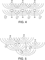
- FIG. 4 is a view for describing influence of interference of diffracted light in a case where the spacers 30 are regularly arranged.
- FIG. 4 illustrates a case where the plurality of spacers 30 are two-dimensionally arranged with respect to two directions, that is, a light traveling direction L and a direction orthogonal to the traveling direction L, but the similar influence is exerted even in a case where the spacers 30 are arranged one-dimensionally in the direction orthogonal to the light traveling direction L.
- the spacers 30 are regularly arranged and the distance between the adjacent spacers 30 (in particular, the distance with respect to the direction orthogonal to the light traveling direction L) is constant as illustrated in FIG. 4 , interference of diffracted light periodically occurs, and a region of visible light is enlarged.
- the diffracted beams of light intensify each other at a constant period if the distance between the adjacent spacers 30 is constant, and thus, the influence of interference of diffracted light increases so that the light from the point light source looks greatly blurred.
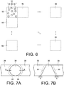
- FIG. 5 is a view for describing influence of interference of diffracted light in a case where the spacers 30 are irregularly (randomly) arranged.
- FIG. 5 illustrates a case where the plurality of spacers 30 are two-dimensionally arranged with respect to two directions, that is, the light traveling direction L and the direction orthogonal to the traveling direction L, but the similar influence is exerted even in a case where the spacers 30 are arranged one-dimensionally in the direction orthogonal to the light traveling direction L.
- the interference of diffracted light does not periodically occur, and the region of visible light does not change.
- an interference zone of diffracted light becomes random and the light intensity of extent where it is difficult to visually recognize the influence of interference of diffracted light is realized if the distance between the adjacent spacers 30 is ununiform, and thus, it is possible to view the light from the point light source with its original size.
- a method of determining specific positions of "the plurality of spacers 30 whose distance to the other spacer 30 positioned at the closest distance is inconstant" is not particularly limited, and can be appropriately determined based on an arbitrary method.
- the specific positions of the plurality of spacers 30 may be determined following a method of defining a generating point of the Voronoi diagram.
- the specific positions of the plurality of spacers 30 may be determined by, for example, defining the maximum value and the minimum value of the distance between the two spacers 30, adjacent to each other, and using these values as constraint conditions.
- all the spacers 30 provided in the light-modulating cell 10 may be randomly arranged with no mutual relation, but the plurality of spacers 30 provided in the light-modulating cell 10 may be configured by repeatedly arranging the unit patterns each of which is formed of a plurality of spacers 30 (three or more spacers 30) arranged with a predetermined relative positional relationship.
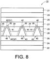
- FIG. 6 is a plan view illustrating a concept of an arrangement example (modified example) of the spacers 30.
- a condition that "the distance to the other spacer 30, positioned at the closest distance, is inconstant" is satisfied with respect to the plurality of spacers 30 (unit patterns 34) included in a predetermined unit pattern area 50.
- the plurality of spacers 30 provided in the light-modulating cells 10 are configured by repeatedly arranging the plurality of spacers 30 (unit patterns 34) included in the unit pattern area 50.
- the unit pattern area 50 is not particularly limited, it is preferable to define a rectangular area defined depending on the entire area where the spacers 30 are provided as the unit pattern area 50, and, for example, it is also possible to define a square area having one side of 10 mm as the unit pattern area 50.
- the specific number and arrangement of the spacers 30 included in the unit pattern area 50 are not particularly limited either.
- this modified example is suitable, for example, when the area where the spacers 30 are provided is wide.
- the spacer 30 according to the present embodiment has the columnar shape as described above, and thus, is excellent in not only a position fixing property, but also an optical alignment property.
- FIGs. 7A and 7B each illustrate an enlarged sectional shape of the liquid crystal layer 29 and the spacer 30, FIG. 7A illustrates a spherical spacer 30, and FIG. 7B illustrates the columnar (truncated conical) spacer 30 illustrated in FIG. 2 .
- the spacer 30 affects the orientation of the liquid crystal layer 29, and thus, the orientation of the liquid crystal layer 29 tends to be disturbed in the vicinity of the spacer 30. Therefore, regions in the vicinity of the spacer 30 indicated by reference sign "35" in FIGs. 7A and 7B become unstable areas relating to the orientation of the liquid crystal layer 29, and the light passing through the unstable area 35 may be polarized in an unintended direction in some cases.
- the columnar spacer 30 When comparing the spherical spacer 30 (see FIG. 7A ) with the columnar spacer 30 (see FIG. 7B ), in general, the columnar spacer 30 has smaller influence (see reference sign "S" in FIGs. 7A and 7B ) on the unstable area 35 than the spherical spacer 30. That is, the unstable area 35 is defined depending on a surface shape of the spacer 30, and a "range where light passes through the unstable area 35 (see reference sign "S" in FIGs.
- the columnar spacer 30 excellent in the position fixing property and optical alignment property as described above it is possible not only to accurately serve the intrinsic function of the spacer such as securing a space between the alignment films (the first alignment film 27 and the second alignment film 28) even under environment where the external force such as vibration is applied, but also to accurately control a polarization state of light passing through the liquid crystal layer 29. Therefore, the light-modulating cell 10 (the spacer 30 (see FIGs. 7A and 7B )) according to this embodiment described above can be suitably used, for example, in a window (for example, a skylight of a house) or the like.
- the skylight of the house or the like does not necessarily have a flat structure in design, and may be required to have a curved structure. Even in such a case, it is also possible to curve all or a part of at least one of the pair of polarizing plates (the first polarizing plate 21 and the second polarizing plate 22), to curve other members (see reference signs "23" to "30" in FIG. 2 ), and to curve the entire light-modulating cell 10 according to the light-modulating cell 10 (spacer 30) of this embodiment described above.
- the specific configuration of the light-modulating cell 10 is not limited to the above-described example, and the present invention is also applicable to another light-modulating cell 10 that includes: a pair of film substrates (a first film substrate 23 and a second film substrate 24); a pair of transparent electrodes (a first transparent electrode 25 and a second transparent electrode 26); a pair of alignment films (a first alignment film 27 and a second alignment film 28); a plurality of spacers 30; and a liquid crystal layer 29.
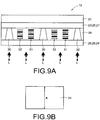
- FIG. 8 is a view illustrating another example of a cross section of the light-modulating cell 10.
- Each of the plurality of spacers 30 in this example has a multilayer structure (two-layer structure in this example), and is provided so as to penetrate through the second alignment film 28 and the liquid crystal layer 29.
- each of the spacers 30 includes a truncated conical core portion 40 and a covering portion 41 covering at least a part of the core portion 40, and penetrates through one of the pair of alignment films (the second alignment film 28 in this example) and the liquid crystal layer 29.
- the covering portion 41 of this example covers an upper surface (upper bottom surface) of the core portion 40 on the first alignment film 27 side and a side surface (outer surface) of the core portion 40 to be interposed between the core portion 40 and the first alignment film 27, between the core portion 40 and the liquid crystal layer 29, and between the core portion 40 and the second alignment film 28.
- the covering portion 41 of this example is formed using the same member as the second alignment film 28 and is formed integrally with the second alignment film 28. Therefore, the "covering portion 41 interposed between the core portion 40 and the second alignment film 28 (see dotted-line portions in FIG. 10 )" substantially forms a part of the second alignment film 28, and practically, there is no boundary surface between the covering portion 41 and the second alignment film 28. On the other hand, a lower surface (lower bottom surface) of the core portion 40 on the second transparent electrode 26 side is in contact with the second transparent electrode 26, and the covering portion 41 is not interposed between the core portion 40 and the second transparent electrode 26.
- each of the spacers 30 of this example has a first support surface 42 that is in two-dimensional contact with the other alignment film (the first alignment film 27 in this example) of the pair of alignment films, and a second support surface 43 being in two-dimensional contact with one of the pair of transparent electrodes (the second transparent electrode 26 in this example).
- the first support surface 42 is formed by the covering portion 41 and forms the above-described first bottom portion 31.
- the second support surface 43 is formed by the core portion 40 and the covering portion 41 (the covering portion 41 integrally formed with the second alignment film 28), and forms the above-described second bottom portion 32.
- the second support surface 43 (the second bottom portion 32) of the spacer 30 is formed by the core portion 40 and the covering portion 41, and only a part of the second support surface 43 is formed by the core portion 40 in this example, but the entire second support surface 43 may be formed by the core portion 40.
- the light-modulating cell 10 of this example it is possible to highly accurately and simply form the spacer 30 based on a photolithography technique to be described later.
- each of the spacers 30 is provided so as to penetrate through the second alignment film 28 and the liquid crystal layer 29. That is, each of the spacers 30 is also supported by the second alignment film 28 so that it is possible to effectively prevent each of the spacers 30 from moving due to an external force or the like.
- the first alignment film 27 and the second alignment film 28 are illustrated to have the same thickness as the liquid crystal layer 29 in the drawing, but the actual first alignment film 27 and second alignment film 28 are formed to be extremely thin.
- each of the spacers 30 has the multilayer structure, it is possible to easily impart various characteristics to each of the spacers 30. For example, it is possible to realize the spacer 30 excellent in surface characteristics while securing high proof stress performance by forming the covering portion 41 with a member having small influence on the liquid crystal layer 29 while forming the core portion 40 of each of the spacers 30 with a member having excellent rigidity.
- each of the spacers 30 has the two-layer structure in the above-described example, but each of the spacers 30 may be configured using three or more layers.
- the periodicity of mutual interference of diffracted light generated by the respective spacers 30 disappears by making a distance between the spacers 30 inconstant, and it is possible to reduce the influence of interference of diffracted light generated by the plurality of spacers 30 and to provide observation light excellent in visibility.
- a liquid crystal layer 29 may contain a dichroic pigment (guest) and a liquid crystal (host).
- the dichroic pigment contained in the liquid crystal layer 29 is preferably a coloring material that has a light shielding property and capable of shielding (absorbing) desired visible light.
- a specific configuration of the light-modulating cell 10 employing the guest-host liquid crystal to which the present invention is applicable is not particularly limited.
- only one polarizing plate may be provided as illustrated in FIGs. 9A to 10B to be described later, or a polarizing plate is not necessarily provided as illustrated in FIGs. 11 and 12 to be described later, instead of providing a pair of polarizing plates (see the first polarizing plate 21 and the second polarizing plate 22 in FIG. 2 ).
- a typical example of the light-modulating cell 10 employing the guest-host liquid crystal will be described.
- FIGs. 9A and 9B are conceptual views for describing an example (light shielding state) of the light-modulating cell 10 employing the guest-host liquid crystal
- FIG. 9A is a cross-sectional view of the light-modulating cell 10
- FIG. 9B is a plan view of a first polarizing plate 21 in which an absorption axis direction is indicated by an arrow "A”.
- FIGs. 10A and 10B are conceptual views for describing the same light-modulating cell 10 (a light transmitting state) as FIGs. 9A and 9B
- FIG. 10A is a cross-sectional view of the light-modulating cell 10
- FIG. 10B is a plan view of the first polarizing plate 21 in which the absorption axis direction is indicated by an arrow "A".
- an absorption axis of the first polarizing plate 21 and a polarization axis (light transmission axis) extend in directions vertical to each other.
- the light-modulating cell 10 of this example has basically the same configuration as that of the light-modulating cell 10 illustrated in FIG. 2 . That is, the light-modulating cell 10 illustrated in FIGs. 9A to 10B also includes: a pair of film substrates (a first film substrate 23 and a second film substrate 24); a pair of transparent electrodes (a first transparent electrode 25 and a second transparent electrode 26) arranged between the pair of film substrates; a pair of alignment films (a first alignment film 27 and a second alignment film 28) arranged between the pair of transparent electrodes; a plurality of spacers 30 supporting at least any one of the pair of alignment films and being in two-dimensional contact with at least any one of the pair of alignment films; and the liquid crystal layer 29 arranged between the plurality of spacers 30 between the pair of alignment films, and in which at least some of the plurality of spacers 30 have an inconstant distance to the other spacer 30 positioned at the closest distance, which is similar to the light-modulating cell 10 illustrated in FIG.
- the liquid crystal layer 29 is configured using the guest-host liquid crystal containing dichroic pigments (dyes) 51 and liquid crystals 52.
- the dichroic pigments 51 exist in a dispersed state in the liquid crystals 52, have the same alignment as the liquid crystals 52, and are basically aligned in the same direction as the liquid crystals 52.
- the dichroic pigment 51 and the liquid crystal 52 are aligned in the horizontal direction (particularly, a direction vertical to the absorption axis direction A of the first polarizing plate 21 (that is, the same direction as the polarization axis of the first polarizing plate 21)) vertical to the light traveling direction L (that is, the stacking direction of the light-modulating cell 10) (see FIG. 9A ).
- FIG. 9A and FIG. 10A conceptually illustrate the dichroic pigment 51 and the liquid crystal 52 in order to illustrate the alignment directions of the dichroic pigment 51 and the liquid crystal 52.
- a desired electric field is not applied to the liquid crystal layer 29, and the dichroic pigment 51 and the liquid crystal 52 are aligned in the horizontal direction (see FIG. 9A ).
- light vibrating in the direction orthogonal to the absorption axis direction A of the first polarizing plate 21 is shielded by the dichroic pigment 51, and light vibrating in the other direction is shielded by the first polarizing plate 21. Therefore, light traveling in the direction from the second film substrate 24 toward the first polarizing plate 21 (see an arrow "L") is shielded by the dichroic pigment 51 and the first polarizing plate 21.
- the spacers 30 of this example are also irregularly arranged and a distance between the adjacent spacers 30 (particularly, a distance in the direction orthogonal to the light traveling direction L) is inconstant, which is similar to the light-modulating cell 10 illustrated in FIG. 2 .
- the interference of diffracted light generated by the respective spacers 30 does not periodically occur, and it is possible to reduce the influence of interference of diffracted light generated by the plurality of spacers 30 and provide observation light excellent in visibility.
- the desired electric field is applied to the liquid crystal layer 29, and the dichroic pigment 51 and the liquid crystal 52 are aligned in the vertical direction (see FIG. 10A ).
- the light shielding performance of the dichroic pigment 51 with respect to the light passing through the liquid crystal layer 29 is hardly exerted regardless of the light vibrating direction, and the light entering the liquid crystal layer 29 passes through the liquid crystal layer 29 (the dichroic pigment 51 and the liquid crystal 52) with a high probability.
- the light vibrating in parallel with the polarization axis (light transmission axis) of the first polarizing plate 21 passes through the first polarizing plate 21 and is emitted from the light-modulating cell 10.
- each of the spacers 30 can include a flat first bottom portion 31, which is made of a photocurable resin and in contact with one (for example, the first alignment film 27) of the pair of alignment films, and a second bottom portion 32 opposing the first bottom portion 31, and have a tapered shape (for example, a taper angle in a range of 75° or larger and 85° or smaller).
- the plurality of spacers 30 may be configured by repeatedly arranging unit patterns (see reference sign "50" in FIG.
- each of the plurality of spacers 30 may include a core portion 40 and a covering portion 41 covering at least a part of the core portion 40, penetrate through one (for example, the second alignment film 28) of the pair of alignment films and the liquid crystal layer 29, and have a first support surface 42 being in two-dimensional contact with the other alignment film (for example, the first alignment film 27) of the pair of alignment films and a second support surface 43 being in two-dimensional contact with one (for example, the second transparent electrode 26) of the pair of electrodes, and the first support surface 42 may be formed by the covering portion 41, and at least a part of the second support surface 43 may be formed by the core portion 40.
- so-called normally black type alignment films 27 and 28 and liquid crystal layer 29 has been described as above regarding the light-modulating cell 10 illustrated in FIGs. 9A to 10B , but so-called normally white type alignment films 27 and 28 and liquid crystal layer 29 may be used. That is, in the case of the normally black type, it is necessary to cause the dichroic pigment 51 and the liquid crystal 52 to be aligned in the vertical direction when the electric field is applied to the liquid crystal layer 29 by applying the voltage between the electrodes 25 and 26 as described above, and thus, a horizontal alignment film is used as the alignment films 27 and 28, and a positive liquid crystal is used for the liquid crystal layer 29.
- the dichroic pigment 51 and the liquid crystal 52 it is necessary to cause the dichroic pigment 51 and the liquid crystal 52 to be aligned in the horizontal direction as illustrated in FIG. 9A when the electric field is applied to the liquid crystal layer 29 by applying the voltage between the electrodes 25 and 26, and thus, a vertical alignment film is used as the alignment films 27 and 28, and a negative liquid crystal is used for the liquid crystal layer 29.
- the above-described operational effect that the influence of the diffracted light generated by the spacer 30 can be reduced by irregularly arranging the spacer 30 is valid not only in the light-modulating cell 10 employing the guest-host liquid crystal of the normally black type but also in the light-modulating cell 10 employing the guest-host liquid crystal of the normally white type.
- FIG. 11 is a conceptual view for describing another example (a light shielding state) of a light-modulating cell 10 employing a guest-host liquid crystal, and illustrates a cross section of the light-modulating cell 10.
- FIG. 12 is a conceptual view for describing the same light-modulating cell 10 (a light transmitting state) as FIG. 11 , and illustrates a cross section of the light-modulating cell 10.
- the light-modulating cell 10 of this example has basically the same configuration as that of the light-modulating cell 10 illustrated in FIG. 2 , but has a liquid crystal layer 29 of the guest-host type containing a dichroic pigment (dye) 51 and a liquid crystal 52 without providing a polarizing plate (a first polarizing plate 21 and a second polarizing plate 22). That is, the dichroic pigments 51 exist in a dispersed state in the liquid crystals 52, have the same alignment as the liquid crystals 52, and are basically aligned in the same direction as the liquid crystals 52.
- the dichroic pigment 51 and the liquid crystal 52 are aligned in the horizontal direction (that is, the direction vertical to the light traveling direction L) (see FIG. 11 ).
- the alignment of the dichroic pigment 51 and the liquid crystal 52 of this example be twisted by 180 degrees or more with respect to the horizontal direction in a state where no electric field is applied so that the dichroic pigments 51 are directed in every horizontal direction.
- FIGs. 11 and 12 conceptually illustrate the dichroic pigment 51 and the liquid crystal 52 in order to illustrate the alignment directions of the dichroic pigment 51 and the liquid crystal 52.
- the spacers 30 of this example are also irregularly arranged and a distance between the adjacent spacers 30 (particularly, a distance in the direction orthogonal to the light traveling direction L) is inconstant, which is similar to the light-modulating cell 10 illustrated in FIG. 2 .
- the interference of diffracted light generated by the respective spacers 30 does not periodically occur, and it is possible to reduce the influence of interference of diffracted light generated by the plurality of spacers 30 and provide observation light excellent in visibility.
- the desired electric field is applied to the liquid crystal layer 29, and the dichroic pigment 51 and the liquid crystal 52 are aligned in the vertical direction (see FIG. 12 ).
- the light shielding performance of the dichroic pigment 51 with respect to the light passing through the liquid crystal layer 29 is hardly exerted regardless of the light vibrating direction, and the light entering the liquid crystal layer 29 passes through the liquid crystal layer 29 (the dichroic pigment 51 and the liquid crystal 52) with a high probability.
- no polarizing plate is provided in this example, the entire light passing through the liquid crystal layer 29 and emitted from a first film substrate 23 is emitted from the light-modulating cell 10.
- the guest-host light-modulating cell 10 of the normally black type in which the horizontal alignment film is used as the alignment films 27 and 28 and the positive liquid crystal is used for the liquid crystal layer 29 has been described as above regarding the light-modulating cell 10 illustrated in FIGs. 11 and 12 , a guest-host light-modulating cell 10 of a normally white type may be used. That is, a vertical alignment film is used as the alignment films 27 and 28, and a negative liquid crystal is used for the liquid crystal layer 29 such that the dichroic pigment 51 and the liquid crystal 52 may be aligned in the horizontal direction as illustrated in FIG. 11 when the electric field is applied to the liquid crystal layer 29 by applying the voltage between the electrodes 25 and 26.
- a method of manufacturing the light-modulating cell 10 according to this embodiment is not particularly limited, and the light-modulating cell 10 can be manufactured using arbitrary bonding technique, photolithography technique, or the like.
- the columnar spacer 30 having the tapered shape can be suitably manufactured by the photolithography technique.
- irradiation with light with respect to a resist is performed using a mask in which a pattern that is defined in accordance with the arrangement of the respective spacers 30 is formed.
- a method of forming the above-described pattern in the mask is not particularly limited, and, for example, it is possible to randomly arrange all lattice points (all the spacers 30) by shifting X-Y coordinates of the respective lattice points (arrangement points of the respective spacers 30) using an arbitrary method on the basis of a pattern of a square lattice.
- the inventor of the present application has observed a diffraction state of light with respect to each of a plurality of kinds of "groups of the spacers 30" having different shift ranges by changing the shift range of each lattice point of the square lattice in order to determine the arrangement of the respective spacers 30.
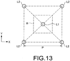
- one side of a square formed by four lattice points that is, “diagonal lattice points L2 (diagonal spacers 30)
- arranged on diagonal lines having each lattice point that is, a "lattice point L1 of interest (the spacer 30 of interest)" as the center in the square lattice, is set as a "diagonal pitch P".
- a limit R of the shift range with respect to the X-Y coordinates of the lattice point L1 of interest (the spacer 30 of interest) was restricted to a size of 10% to 50% of the diagonal pitch P, and the arrangement of the lattice points L1 of interest (the spacers 30 of interest) was randomly shifted by using random numbers.
- the "spacer 30 of interest” does not indicate only the specific spacer 30 among all the spacers 30, but each of all the spacers 30 is treated as the "spacer 30 of interest” referred to herein.
- the arrangement of all the spacers 30 is randomly shifted by determining the arrangement of the respective spacers 30 as described above based on positions of the diagonal lattice points L2 (diagonal spacers 30) allocated to each of the spacers 30.
- the arrangement of all the spacers 30 is shifted using the "method of shifting the arrangement of the spacers 30 of interest based on the positions of the diagonal lattice points L2" in this manner, it is possible to randomly arrange all the spacers 30.
- a process of coating the top of the second transparent electrode 26 with a photosensitive resin (photocurable resin) forming the spacer 30, forming the tapered spacer 30 using the photosensitive resin by the photolithography technique, and then, forming the second alignment film 28 on the second transparent electrode 26, and imparting an alignment regulating force to the second alignment film 28 by rubbing or the like may be performed.
- the alignment imparting process is performed with respect to the second alignment film 28 in the state where the spacer 30 has been formed.
- the alignment imparting process for the second alignment film 28 is performed in a state where the "inverted tapered spacer 30" in which the bottom portion (first bottom portion 31) of each of the spacers 30 on the first alignment film 27 side is larger than the bottom portion (second bottom portion 32) on the second alignment film 28 side is formed, it is sometimes difficult to impart the sufficient alignment with respect to the second alignment film 28 in the vicinity of the spacer 30. Therefore, the "forward tapered spacer 30" in which the bottom portion (first bottom portion 31) of each of the spacers 30 on the first alignment film 27 side is smaller than the bottom portion (second bottom portion 32) on the second alignment film 28 side is preferable from the viewpoint of imparting the alignment with respect to the second alignment film 28.
- a light-modulating cell 10 of this example is the light-modulating cell 10 that controls transmitted light using a liquid crystal.
- a liquid crystal layer 29 was sandwiched between films for liquid crystal orientation layers (a first alignment film 27 and a second alignment film 28) to prepare a liquid crystal cell, and the liquid crystal cell was sandwiched between linearly polarizing plates (a first polarizing plate 21 and a second polarizing plate 22) arranged in a parallel nicol state, thereby producing the light-modulating cell 10 of this example.
- the light-modulating cell 10 of this example has the same layer structure as the light-modulating cell 10 illustrated in FIG.
- a film-shaped resin substrate (particularly, a film substrate made of polycarbonate in this example) was used as the first film substrate 23 supporting the first transparent electrode 25 and the second film substrate 24 supporting the second transparent electrode 26.
- the films for liquid crystal orientation layers were formed by sequentially producing electrodes (the first transparent electrode 25 and the second transparent electrode 26) and alignment layers (the first alignment film 27 and the second alignment film 28) with respect to the film member (substrate).
- the light from the point light source was affected by interference of diffracted light generated by the respective spacers 30, and a light interference region was generated around the point light source.
- Each of spacers 30 (all spacers 30) used in a light-modulating cell 10 of this example was arranged so as to have an inconstant distance to the other spacer 30 positioned at the closest distance.
- the other configurations of the light-modulating cell 10 of this example are the same as those of the above-described Specific Example 1 (comparative example).
- Embodiments of the present invention are not limited to the individual embodiments described above, but include various modifications that can be conceived by those skilled in the art, and the effects of the present invention are not limited to the above-described content. That is, various additions, modifications, and partial deletions can be made in a scope not departing from the conceptual idea and gist of the present invention derived from the content defined in the claims and their equivalents.
Landscapes
- Physics & Mathematics (AREA)
- Nonlinear Science (AREA)
- Chemical & Material Sciences (AREA)
- Crystallography & Structural Chemistry (AREA)
- General Physics & Mathematics (AREA)
- Optics & Photonics (AREA)
- Mathematical Physics (AREA)
- Spectroscopy & Molecular Physics (AREA)
- Engineering & Computer Science (AREA)
- Civil Engineering (AREA)
- Structural Engineering (AREA)
- Geometry (AREA)
- Materials Engineering (AREA)
- Organic Chemistry (AREA)
- Liquid Crystal (AREA)
Abstract
Description
- The present invention relates to a light-modulating cell that controls liquid crystal orientation to perform light modulation.
- For example, an electronic blind or the like in which a light-modulating cell (light-modulating material) is installed in a window, a door, or the like, and the transmission of extraneous light is controlled by the light-modulating cell has been known. It is possible to suitably employ a liquid crystal, for example, as such a light-modulating cell.
- The light-modulating cell employing the liquid crystal is produced by, for example, sandwiching a liquid crystal layer between a pair of transparent film members forming transparent electrodes or between a pair of alignment films so as to prepare a liquid crystal cell, and sandwiching this liquid crystal cell between linear polarizing plates to take linearly polarized light. When light-modulating is performed by using a light-modulating cell employing a liquid crystal, the transmission of light is controlled by controlling an electric field to be applied to the liquid crystal layer to change orientation of liquid crystal molecules contained in the liquid crystal layer, and the light-modulating cell can switch the shielding and transmission of extraneous light and continuously change the amount of transmitted light, for example.
- For example,
Patent Literature 1 discloses a liquid crystal panel that is provided in a window or a door of a house and capable of controlling a transparent state and an opaque state. According to this liquid crystal panel, a plurality of divided liquid crystal panels are juxtaposed, and each of the divided liquid crystal panels can be individually controlled between the transparent state and the opaque state. - In addition, Patent Literature 2 discloses a light control glass window capable of adjusting light transmittance in various patterns in accordance with a change of a sunlight situation. According to this light control glass window, the light transmittance can be adjusted by changing a voltage acting on a liquid crystal sealed between two transparent glass plates to change optical characteristics of the liquid crystal.
-
- Patent Literature 1: Japanese patent application publication No.
03-47392 - Patent Literature 2: Japanese patent application publication No.
08-184273 - In a light-modulating cell having a liquid crystal cell, there is a case where a spacer is provided between the pair of transparent film members (alignment films) forming the liquid crystal cell, and the liquid crystal layer is held at a desired thickness by the spacer. In this case, it is possible to produce an alignment layer by, for example, preparing the spacer, and then, creating a thin film of polyimide or the like and subjecting the thin film to rubbing, and it is possible to regulate the orientation of a liquid crystal material with this alignment layer.
- Such a spacer can be formed using various methods, and it is possible to accurately form a large number of spacers, regularly arranged, at once, for example, based on a photolithography technique. In general, all the spacers are regularly arranged and a distance between the spacers is adjusted to be constant in order to simply and accurately form the multiple spacers.
- However, as a result of earnest research, the inventors of the present application have found that, when the regularity relating to the arrangement of the spacers is high and the distance between the spacers is constant, the intervals at which lights diffracted by the respective spacers interfere with each other and intensify each other also become regular, so that a point light source may be recognized as blurred light. That is, when the spacers are regularly arranged, the interference of the diffracted light generated by the spacers periodically occurs and the diffracted beams of light periodically intensify each other, and thus, the point light source looks larger than the original size so that the visibility of observation light that has passed through the light-modulating cell deteriorates.
- Therefore, it is desired to propose a new method for reducing influence of the interference of diffracted light generated by the spacers in the light-modulating cell provided with the multiple spacers so as to provide the observation light excellent in visibility. In particular, there is a request for reduction of the influence of interference of diffracted light generated by the spacers in order to provide the observation light excellent in visibility even in a liquid crystal cell employing a guest-host liquid crystal, which has attracted attention in recent years. However, a proposal effective in satisfying such a request has not been made in the related art literatures (for example, the above-described
Patent Literatures 1 and 2). - The present invention has been made in view of the above-described circumstances, and an object of the present invention is to provide a light-modulating cell that is capable of reducing influence of interference of diffracted light generated by a plurality of spacers and providing observation light excellent in visibility.
- Another object of the present invention is to provide a light-modulating cell employing a guest-host liquid crystal that is capable of reducing influence of interference of diffracted light generated by a plurality of spacers and providing observation light excellent in visibility.
- One aspect of the present invention is directed to a light-modulating cell comprising: a pair of polarizing plates; a pair of film substrates arranged between the pair of polarizing plates; a pair of electrodes arranged between the pair of polarizing plates; a pair of alignment films arranged between the pair of electrodes; a plurality of spacers supporting at least any one of the pair of alignment films and being in two-dimensional contact with at least any one of the pair of alignment films; and a liquid crystal layer arranged between the plurality of spacers between the pair of alignment films, wherein at least some of the plurality of spacers have an inconstant distance to another spacer positioned at a closest distance.
- According to this aspect, the distance between the spacers is inconstant, and therefore it is possible to reduce the influence of interference of diffracted light generated by the plurality of spacers and to provide the observation light excellent in visibility.
- Another aspect of the present invention is directed to a light-modulating cell comprising: a pair of film substrates; a pair of electrodes arranged between the pair of film substrates; a pair of alignment films arranged between the pair of electrodes; a plurality of spacers supporting at least any one of the pair of alignment films and being in two-dimensional contact with at least any one of the pair of alignment films; and a liquid crystal layer arranged between the plurality of spacers between the pair of alignment films, wherein the liquid crystal layer contains at least a dichroic pigment, and at least some of the plurality of spacers have an inconstant distance to another spacer positioned at a closest distance.
- The light-modulating cell may further include a polarizing plate provided on the opposite side of the pair of electrodes with one of the pair of film substrates interposed therebetween.
- Each of the plurality of spacers may have a flat first bottom portion in contact with one of the pair of alignment films and a second bottom portion opposing the first bottom portion.
- According to this aspect, the alignment film can be accurately supported by each spacer. Incidentally, it is possible to suitably form the plurality of spacers according to this aspect based on, for example, a photolithography technique.
- The plurality of spacers may be made of a photocurable resin.
- According to this aspect, it is possible to easily form each spacer by utilizing the photocuring performance of the photocurable resin. Incidentally, it is possible to suitably form the plurality of spacers according to this aspect based on, for example, a photolithography technique.
- The plurality of spacers may be configured by repeatedly arranging unit patterns each of which is formed of three or more spacers arranged with a predetermined relative positional relationship.
- According to this aspect, it is possible to easily form the plurality of spacers while reducing the influence of interference of diffracted light generated by the plurality of spacers.
- Each of the plurality of spacers may have a tapered shape that tapers from one of the pair of alignment films toward the other alignment film.
- According to this aspect, the alignment film can be accurately supported by the respective spacers.
- A taper angle of each of the plurality of spacers may be in a range of 75° or larger and 85° or smaller.
- According to this aspect, an appropriate alignment regulating force can be imparted to the liquid crystal layer by the alignment film while accurately supporting the alignment film with the respective spacers.
- At least any one of the pair of polarizing plates may be partially or entirely curved.
- At least any one of the pair of film substrates may be partially or entirely curved.
- According to these aspects, the light-modulating cell can be applied to a curved structure.
- Each of the plurality of spacers may include a core portion and a covering portion covering at least a part of the core portion, penetrate through one of the pair of alignment films and the liquid crystal layer, and have a first support surface being in two-dimensional contact with the other alignment film of the pair of alignment films and a second support surface being in two-dimensional contact with one of the pair of electrodes, and the first support surface may be formed by the covering portion, and at least a part of the second support surface may be formed by the core portion.
- According to this aspect, it is possible to accurately form the respective spacers based on a so-called photolithography technique.
- According to the present invention, the distance between spacers is inconstant, and therefore the periodicity in mutual interference of diffracted light generated by the respective spacers disappears. Thus, the influence of interference of diffracted light generated by the plurality of spacers is reduced, and the observation light excellent in visibility can be created.
-
-
FIG. 1 is a conceptual diagram illustrating an example of a light-modulating system. -
FIG. 2 is a view illustrating an example of a cross section of a light-modulating cell. -
FIG. 3 is a view for describing a taper angle of each spacer. -
FIG. 4 is a view for describing influence of interference of diffracted light in a case where the spacers are regularly arranged. -
FIG. 5 is a view for describing influence of interference of diffracted light in a case where the spacers are irregularly (randomly) arranged. -
FIG. 6 is a plan view illustrating a concept of an arrangement example (modified example) of the spacers. -
FIGs. 7A and 7B each illustrate an enlarged sectional shape of a liquid crystal layer and a spacer,FIG. 7A illustrates a spherical spacer, andFig. 7B illustrates a columnar (truncated conical) spacer illustrated inFIG. 2 . -
FIG. 8 is a view illustrating another example of a cross section of a light-modulating cell. -
FIGs. 9A and 9B are conceptual views for describing an example (light shielding state) of a light-modulating cell employing a guest-host liquid crystal,FIG. 9A is a cross-sectional view of the light-modulating cell, andFIG. 9B is a plan view of a first polarizing plate in which an absorption axis direction is indicated by an arrow "A". -
FIGs. 10A and 10B are conceptual views for describing the same light-modulating cell (a light transmitting state) asFIGs. 9A and 9B ,FIG. 10A is a cross-sectional view of the light-modulating cell, andFIG. 10B is a plan view of the first polarizing plate in which the absorption axis direction is indicated by an arrow "A". -
FIG. 11 is a conceptual view for describing another example (a light shielding state) of the light-modulating cell employing the guest-host liquid crystal, and illustrates a cross section of the light-modulating cell. -
FIG. 12 is a conceptual view for describing the same light-modulating cell (a light transmitting state) asFIG. 11 , and illustrates a cross section of a light-modulatingcell 10. -
FIG. 13 is a view for describing an example of a method of determining a mask pattern. - Hereinafter, an embodiment of the present invention will be described with reference to the drawings. In the drawings attached to the specification of the present application, a scale, a dimensional ratio, and the like of each element are conveniently exaggerated and changed from the actual scale, dimensional ratio, and the like in order to facilitate the illustration and understanding. In addition, in this specification, the terms "plate", "sheet", and "film" are not distinguished from each other based solely on differences in nomenclature. For example, the term "plate" is a concept that also includes a member which can be called a sheet or a film. In addition, the terms specifying shapes, geometric conditions, and extent thereof used in this specification (for example, terms such as "parallel", "orthogonal", and "same", values of a length and an angle, and the like) are understood as terms meaning ranges of extent where substantially the equivalent or similar functions can be expected without being bound by strict meaning.
-
FIG. 1 is a conceptual diagram illustrating an example of a light-modulatingsystem 5. - A light-modulating
cell 10 of this example has a layer made of a liquid crystal material containing liquid crystal molecules as will be described later, and can switch shielding and transmission of light and change the transmittance (transmissivity) of light. An object to which the light-modulatingcell 10 is applied is not particularly limited, and typically, the light-modulatingcell 10 can be applied to a window, a door, and the like. In particular, a columnar spacer to be described later is excellent in position fixing performance, and a position thereof is hardly varied by an external force such as vibration. Therefore, the light-modulatingcell 10 having the columnar spacer to be described later can be suitably used even under environment where the external force such as vibration is applied, and can also be applied to a window (for example, a skylight) installed in a house. - The light-modulating
cell 10 is connected to a light-modulatingcontroller 12, and a sensor device 14 and auser operation unit 16 are connected to the light-modulatingcontroller 12. The light-modulatingcontroller 12 controls a light-modulating state of the light-modulatingcell 10 and can switch the shielding and transmission of light using the light-modulatingcell 10 and change the light transmittance in the light-modulatingcell 10. Specifically, the light-modulatingcontroller 12 can switch the shielding and transmission of light using the light-modulatingcell 10 and change the light transmittance by adjusting an electric field to be applied to a liquid crystal layer of the light-modulatingcell 10 to change orientation of the liquid crystal molecules in the liquid crystal layer. - The light-modulating
controller 12 can adjust the electric field to be applied to the liquid crystal layer based on an arbitrary method. For example, the light-modulatingcontroller 12 can switch the shielding and transmission of light using the light-modulatingcell 10 and change the light transmittance by adjusting the electric field to be applied to the liquid crystal layer in accordance with a measurement result of the sensor device 14 or an instruction (command) input by a user via theuser operation unit 16. Therefore, the light-modulatingcontroller 12 may automatically adjust the electric field to be applied to the liquid crystal layer in accordance with the measurement result of the sensor device 14 or may manually adjust the electric field in accordance with the instruction of the user input via theuser operation unit 16. Incidentally, an object to be measured by the sensor device 14 is not particularly limited, and, for example, the brightness of use environment may be measured, and in this case, the switching of the shielding and transmission of light using the light-modulatingcell 10 and the change of the light transmittance are performed in accordance with the brightness of use environment. In addition, it is not always necessary for both the sensor device 14 and theuser operation unit 16 to be connected to the light-modulatingcontroller 12, and any one of the sensor device 14 and theuser operation unit 16 may be connected to the light-modulatingcontroller 12. -
FIG. 2 is a view illustrating an example of a cross section of the light-modulatingcell 10. - The light-modulating
cell 10 of this example includes: a pair of polarizing plates (a firstpolarizing plate 21 and a second polarizing plate 22); a pair of transparent electrodes (a firsttransparent electrode 25 and a second transparent electrode 26) arranged between the pair of polarizing plates; and a pair of alignment films (afirst alignment film 27 and a second alignment film 28) arranged between the pair of transparent electrodes. In addition, a pair of film substrates (afirst film substrate 23 and a second film substrate 24) are arranged at each outer side of the pair of transparent electrodes (the firsttransparent electrode 25 and the second transparent electrode 26) between the pair of polarizing plates (the firstpolarizing plate 21 and the second polarizing plate 22) in this example. That is, the pair of transparent electrodes (the firsttransparent electrode 25 and the second transparent electrode 26) are arranged between the pair of film substrates (thefirst film substrate 23 and the second film substrate 24), and the pair of polarizing plates (the firstpolarizing plate 21 and the second polarizing plate 22) are arranged at each outer side of the pair of film substrates (thefirst film substrate 23 and the second film substrate 24). - Furthermore, a plurality of
columnar spacers 30, which support at least any one of the pair of alignment films (thefirst alignment film 27 in this example) and are in two-dimensional contact with, that is, surface contact with at least any one of the pair of alignment films (thefirst alignment film 27 in this example), are provided in this example. In addition, portions among the plurality ofspacers 30 are filled with liquid crystal layers 29 between the pair of alignment films (thefirst alignment film 27 and the second alignment film 28). - Incidentally, the plurality of
spacers 30 preferably extend at least between a "boundary surface Sb2 between thefirst alignment film 27 and theliquid crystal layer 29" and a "boundary surface Sb1 between thesecond alignment film 28 and theliquid crystal layer 29". Therefore, for example, the plurality ofspacers 30 may be arranged only between thefirst alignment film 27 and thesecond alignment film 28. In addition, the plurality of spacers may be provided so as to penetrate through thesecond alignment film 28 and theliquid crystal layer 29 from the second transparent electrode 26 (a "boundary surface Sb3 between the secondtransparent electrode 26 and thesecond alignment film 28" in the example illustrated inFIG. 2 ) and be in contact with thefirst alignment film 27 as indicated by reference sign "30a" inFIG. 2 Incidentally, it is possible to apply the present invention in the same manner in both the case where thespacer 30 is provided only between thefirst alignment film 27 and thesecond alignment film 28 and the case where the spacer indicated byreference sign 30a ofFIG. 2 is provided. - Each of the first
polarizing plate 21 and the secondpolarizing plate 22 has a unique polarization axis and a unique absorption axis, and allows only light polarized in a specific direction to pass therethrough. For example, when light traveling in a direction from the secondpolarizing plate 22 to the first polarizing plate 21 (see an arrow "L" inFIG. 2 ) is incident on the light-modulatingcell 10, only light polarized in the same direction as the polarization axis of the secondpolarizing plate 22 out of the light passes through the secondpolarizing plate 22 and enters thesecond film substrate 24, and further, only light polarized in the same direction as the polarization axis of the firstpolarizing plate 21 out of the light traveling from thefirst film substrate 23 toward the firstpolarizing plate 21 passes through the firstpolarizing plate 21 and travels toward the outside. An arrangement form of the firstpolarizing plate 21 and the secondpolarizing plate 22 is not particularly limited, and the arrangement form of the firstpolarizing plate 21 and the secondpolarizing plate 22 is determined in relation to an alignment state of the liquid crystal molecules contained in theliquid crystal layer 29. Representative examples thereof include a state called "cross nicol" where the firstpolarizing plate 21 and the secondpolarizing plate 22 are arranged so as to have the polarization axes orthogonal to each other and a state called "parallel nicol" where the firstpolarizing plate 21 and the secondpolarizing plate 22 are arranged so as to have the polarization axes parallel to each other. - For example, when it is desired to improve the rigidity of the light-modulating
cell 10, thefirst film substrate 23 and thesecond film substrate 24 are configured using a transparent member having excellent rigidity. In addition, it is easy to perform "bonding of the light-modulatingcell 10 to a curved surface", which is difficult in the case of using a glass substrate, by using thefirst film substrate 23 andsecond film substrate 24 each of which has a sufficiently flexible film shape. - The first
transparent electrode 25 and the secondtransparent electrode 26 apply a desired electric field to theliquid crystal layer 29 as a voltage is applied thereto by the light-modulating controller 12 (seeFIG. 1 ). Each member forming the firsttransparent electrode 25 or the secondtransparent electrode 26 and an arrangement form of the firsttransparent electrode 25 and the secondtransparent electrode 26 are not particularly limited. For example, the firsttransparent electrode 25 and the secondtransparent electrode 26 can be formed using a member excellent in visible light transmissivity and conductivity such as indium tin oxide (ITO). - The
first alignment film 27 and thesecond alignment film 28 are members configured to align the liquid crystal molecules contained in theliquid crystal layer 29 in a desired direction. Although a method of aligning theliquid crystal layer 29 according to thefirst alignment film 27 and thesecond alignment film 28 is not particularly limited, a twisted nematic (TN) liquid crystal in which molecular arrangement (molecular orientation) is twisted by 90 degrees is used in this example. Incidentally, a method of imparting alignment functions of thefirst alignment film 27 and thesecond alignment film 28 is not particularly limited, and, for example, alignment directions of thefirst alignment film 27 and thesecond alignment film 28 may be defined by rubbing using a member such as nylon, or the alignment directions of thefirst alignment film 27 and thesecond alignment film 28 may be defined by irradiation with linearly polarized ultraviolet rays. - Each of the plurality of
spacers 30 is in surface contact with at least any one of the pair of alignment films (thefirst alignment film 27 in this example), and has a tapered shape that tapers from one of the pair of alignment films (thesecond alignment film 28 in this example) toward the other alignment film (thefirst alignment film 27 in this example). In this example, each of the plurality ofspacers 30 has a flat firstbottom portion 31 in contact with one of a pair of alignment films (thefirst alignment film 27 in this example) and asecond bottom portion 32 opposing thefirst bottom portion 31. Incidentally, a portion of each of thespacers 30 on the boundary surface Sb1 between thesecond alignment film 28 and theliquid crystal layer 29 is illustrated as thesecond bottom portion 32 for the sake of convenience inFIG. 2 , but a portion of each of thespacers 30 on the boundary surface Sb3 between thesecond alignment film 28 and the secondtransparent electrode 26 may be regarded as thesecond bottom portion 32 when each of thespacers 30 extends from the boundary surface Sb3 between thesecond alignment film 28 and the secondtransparent electrode 26 as indicated by reference sign "30a". - The
spacer 30 illustrated inFIG. 2 has a truncated conical shape in which a diameter linearly changes in accordance with a distance from thesecond alignment film 28 and an angle of a side surface is substantially constant, but is not limited thereto. The diameter of thespacer 30 may change nonlinearly in accordance with the distance from thesecond alignment film 28, and, for example, the diameter may change exponentially with respect to the distance from thesecond alignment film 28, or the diameter may change in proportion to a square root of the distance from thesecond alignment film 28. In addition, thespacer 30 has the tapered shape (forward tapered shape) that tapers from thesecond alignment film 28 toward thefirst alignment film 27 in the example illustrated inFIG. 2 , but may have a tapered shape (inverted tapered shape) that tapers from thefirst alignment film 27 toward thesecond alignment film 28. - Incidentally, a taper angle θ of each of the plurality of
spacers 30 is preferably in a range of 75° or larger and 85° or smaller from the viewpoint of realizing the desired orientation of theliquid crystal layer 29 while securing the function as the spacer. -
FIG. 3 is a view for describing the taper angle θ of each of thespacers 30. The taper angle θ of each of thespacers 30 referred to herein is represented by an angle formed between a tangent Lt of a side portion Lp of each of thespacers 30 at a position, separated from the lowermost position of each of thespacers 30 by one third (1/3) of a distance between both end portions of each of the spacers 30 (between the uppermost position (the first bottom portion 31) and the lowermost position (the second bottom portion 32) of each of thespacers 30 inFIG. 3 ) with respect to a stacking direction in a cross section of each of thespacers 30, and a line H extending in the horizontal direction vertical to the stacking direction. That is, the taper angle θ of each of thespacers 30 is represented by the angle formed between the tangent Lt of the portion Lp of a side surface of each of thespacers 30, separated from thesecond bottom portion 32 by the distance corresponding to one third of the entire length of each of thespacers 30 in the stacking direction, and the line H extending in the horizontal direction. - In addition, at least some of the plurality of
spacers 30 have an inconstant distance to theother spacer 30 positioned at the closest distance in the present embodiment. That is, in the example illustrated inFIG. 2 , a "distance (interval) D1 between thecenter spacer 30 and theleft spacer 30" and a "distance D2 between thecenter spacer 30 and theright spacer 30" satisfy a relationship "D1 ≠ D2". - The distance between the
spacers 30 indicating the "distance to theother spacer 30 positioned at the closest distance" is typically represented by the closest distance between thespacers 30. For example, in the case of thespacer 30 having the forward tapered shape illustrated inFIG. 2 (that is, a size of thefirst bottom portion 31 < a size of the second bottom portion 32), the "distance between thespacers 30" is represented by a distance between thesecond bottom portions 32. On the other hand, in the case of thespacer 30 having the inverted tapered shape (that is, the size of thefirst bottom portion 31 > the size of the second bottom portion 32), the "distance between thespacers 30" is represented by a distance between thefirst bottom portions 31. -
FIG. 4 is a view for describing influence of interference of diffracted light in a case where thespacers 30 are regularly arranged. Incidentally,FIG. 4 illustrates a case where the plurality ofspacers 30 are two-dimensionally arranged with respect to two directions, that is, a light traveling direction L and a direction orthogonal to the traveling direction L, but the similar influence is exerted even in a case where thespacers 30 are arranged one-dimensionally in the direction orthogonal to the light traveling direction L. - When the
spacers 30 are regularly arranged and the distance between the adjacent spacers 30 (in particular, the distance with respect to the direction orthogonal to the light traveling direction L) is constant as illustrated inFIG. 4 , interference of diffracted light periodically occurs, and a region of visible light is enlarged. Thus, when assuming light from a point light source, the diffracted beams of light intensify each other at a constant period if the distance between theadjacent spacers 30 is constant, and thus, the influence of interference of diffracted light increases so that the light from the point light source looks greatly blurred. -
FIG. 5 is a view for describing influence of interference of diffracted light in a case where thespacers 30 are irregularly (randomly) arranged. Incidentally,FIG. 5 illustrates a case where the plurality ofspacers 30 are two-dimensionally arranged with respect to two directions, that is, the light traveling direction L and the direction orthogonal to the traveling direction L, but the similar influence is exerted even in a case where thespacers 30 are arranged one-dimensionally in the direction orthogonal to the light traveling direction L. - When the
spacers 30 are irregularly arranged and the distance between the adjacent spacers 30 (in particular, the distance with respect to the direction orthogonal to the light traveling direction L) is inconstant as illustrated inFIG. 5 , the interference of diffracted light does not periodically occur, and the region of visible light does not change. Thus, when assuming the light from the point light source, an interference zone of diffracted light becomes random and the light intensity of extent where it is difficult to visually recognize the influence of interference of diffracted light is realized if the distance between theadjacent spacers 30 is ununiform, and thus, it is possible to view the light from the point light source with its original size. - Therefore, it is possible to reduce the influence of interference of diffracted light generated by the plurality of
spacers 30 and to provide the observation light excellent in visibility by using the light-modulatingcell 10 in which "at least some of the plurality ofspacers 30 have the inconstant distance to theother spacer 30 positioned at the closest distance" according to the present embodiment. - A method of determining specific positions of "the plurality of
spacers 30 whose distance to theother spacer 30 positioned at the closest distance is inconstant" is not particularly limited, and can be appropriately determined based on an arbitrary method. For example, the specific positions of the plurality ofspacers 30 may be determined following a method of defining a generating point of the Voronoi diagram. In addition, the specific positions of the plurality ofspacers 30 may be determined by, for example, defining the maximum value and the minimum value of the distance between the twospacers 30, adjacent to each other, and using these values as constraint conditions. - Incidentally, it is unnecessary for all the
spacers 30 provided in the light-modulatingcell 10 to satisfy the condition that the "distance to theother spacer 30 positioned at the closest distance is inconstant", and it is possible to reduce the influence of interference of diffracted light and to provide the observation light excellent in visibility even when only some of thespacers 30 satisfy the condition that the "distance to theother spacer 30 positioned at the closest distance is inconstant". - In addition, all the
spacers 30 provided in the light-modulatingcell 10 may be randomly arranged with no mutual relation, but the plurality ofspacers 30 provided in the light-modulatingcell 10 may be configured by repeatedly arranging the unit patterns each of which is formed of a plurality of spacers 30 (three or more spacers 30) arranged with a predetermined relative positional relationship. -
FIG. 6 is a plan view illustrating a concept of an arrangement example (modified example) of thespacers 30. In the example illustrated inFIG. 6 , a condition that "the distance to theother spacer 30, positioned at the closest distance, is inconstant" is satisfied with respect to the plurality of spacers 30 (unit patterns 34) included in a predeterminedunit pattern area 50. Further, the plurality ofspacers 30 provided in the light-modulatingcells 10 are configured by repeatedly arranging the plurality of spacers 30 (unit patterns 34) included in theunit pattern area 50. Although a shape and a size of theunit pattern area 50 are not particularly limited, it is preferable to define a rectangular area defined depending on the entire area where thespacers 30 are provided as theunit pattern area 50, and, for example, it is also possible to define a square area having one side of 10 mm as theunit pattern area 50. In addition, the specific number and arrangement of thespacers 30 included in theunit pattern area 50 are not particularly limited either. - As the plurality of spacers 30 (unit patterns 34) included in the
unit pattern area 50 are repeatedly arranged in this manner, it is possible to easily provide a large number of thespacers 30 while effectively reducing the influence of interference of diffracted light generated by therespective spacers 30. Therefore, this modified example is suitable, for example, when the area where thespacers 30 are provided is wide. - Incidentally, the
spacer 30 according to the present embodiment has the columnar shape as described above, and thus, is excellent in not only a position fixing property, but also an optical alignment property. -
FIGs. 7A and 7B each illustrate an enlarged sectional shape of theliquid crystal layer 29 and thespacer 30,FIG. 7A illustrates aspherical spacer 30, andFIG. 7B illustrates the columnar (truncated conical) spacer 30 illustrated inFIG. 2 . In general, thespacer 30 affects the orientation of theliquid crystal layer 29, and thus, the orientation of theliquid crystal layer 29 tends to be disturbed in the vicinity of thespacer 30. Therefore, regions in the vicinity of thespacer 30 indicated by reference sign "35" inFIGs. 7A and 7B become unstable areas relating to the orientation of theliquid crystal layer 29, and the light passing through theunstable area 35 may be polarized in an unintended direction in some cases. When comparing the spherical spacer 30 (seeFIG. 7A ) with the columnar spacer 30 (seeFIG. 7B ), in general, thecolumnar spacer 30 has smaller influence (see reference sign "S" inFIGs. 7A and 7B ) on theunstable area 35 than thespherical spacer 30. That is, theunstable area 35 is defined depending on a surface shape of thespacer 30, and a "range where light passes through the unstable area 35 (see reference sign "S" inFIGs. 7A and 7B )" tends to be larger in the "spherical spacer 30 (having a tangent in the same direction as the light traveling direction)" than in thecolumnar spacer 30 having a tapered shape (not having the tangent in the same direction as the light traveling direction)". - According to the
columnar spacer 30 excellent in the position fixing property and optical alignment property as described above, it is possible not only to accurately serve the intrinsic function of the spacer such as securing a space between the alignment films (thefirst alignment film 27 and the second alignment film 28) even under environment where the external force such as vibration is applied, but also to accurately control a polarization state of light passing through theliquid crystal layer 29. Therefore, the light-modulating cell 10 (the spacer 30 (seeFIGs. 7A and 7B )) according to this embodiment described above can be suitably used, for example, in a window (for example, a skylight of a house) or the like. In particular, the skylight of the house or the like does not necessarily have a flat structure in design, and may be required to have a curved structure. Even in such a case, it is also possible to curve all or a part of at least one of the pair of polarizing plates (the firstpolarizing plate 21 and the second polarizing plate 22), to curve other members (see reference signs "23" to "30" inFIG. 2 ), and to curve the entire light-modulatingcell 10 according to the light-modulating cell 10 (spacer 30) of this embodiment described above. - The specific configuration of the light-modulating
cell 10 is not limited to the above-described example, and the present invention is also applicable to another light-modulatingcell 10 that includes: a pair of film substrates (afirst film substrate 23 and a second film substrate 24); a pair of transparent electrodes (a firsttransparent electrode 25 and a second transparent electrode 26); a pair of alignment films (afirst alignment film 27 and a second alignment film 28); a plurality ofspacers 30; and aliquid crystal layer 29. -
FIG. 8 is a view illustrating another example of a cross section of the light-modulatingcell 10. Each of the plurality ofspacers 30 in this example has a multilayer structure (two-layer structure in this example), and is provided so as to penetrate through thesecond alignment film 28 and theliquid crystal layer 29. - That is, each of the
spacers 30 includes a truncatedconical core portion 40 and a coveringportion 41 covering at least a part of thecore portion 40, and penetrates through one of the pair of alignment films (thesecond alignment film 28 in this example) and theliquid crystal layer 29. As illustrated inFIG. 8 , the coveringportion 41 of this example covers an upper surface (upper bottom surface) of thecore portion 40 on thefirst alignment film 27 side and a side surface (outer surface) of thecore portion 40 to be interposed between thecore portion 40 and thefirst alignment film 27, between thecore portion 40 and theliquid crystal layer 29, and between thecore portion 40 and thesecond alignment film 28. Incidentally, the coveringportion 41 of this example is formed using the same member as thesecond alignment film 28 and is formed integrally with thesecond alignment film 28. Therefore, the "coveringportion 41 interposed between thecore portion 40 and the second alignment film 28 (see dotted-line portions inFIG. 10 )" substantially forms a part of thesecond alignment film 28, and practically, there is no boundary surface between the coveringportion 41 and thesecond alignment film 28. On the other hand, a lower surface (lower bottom surface) of thecore portion 40 on the secondtransparent electrode 26 side is in contact with the secondtransparent electrode 26, and the coveringportion 41 is not interposed between thecore portion 40 and the secondtransparent electrode 26. - Therefore, each of the
spacers 30 of this example has afirst support surface 42 that is in two-dimensional contact with the other alignment film (thefirst alignment film 27 in this example) of the pair of alignment films, and asecond support surface 43 being in two-dimensional contact with one of the pair of transparent electrodes (the secondtransparent electrode 26 in this example). Thefirst support surface 42 is formed by the coveringportion 41 and forms the above-described firstbottom portion 31. In addition, thesecond support surface 43 is formed by thecore portion 40 and the covering portion 41 (the coveringportion 41 integrally formed with the second alignment film 28), and forms the above-described secondbottom portion 32. Incidentally, the second support surface 43 (the second bottom portion 32) of thespacer 30 is formed by thecore portion 40 and the coveringportion 41, and only a part of thesecond support surface 43 is formed by thecore portion 40 in this example, but the entiresecond support surface 43 may be formed by thecore portion 40. - The other configurations are the same as those of the light-modulating
cell 10 illustrated inFIG. 2 , and the same or similar configurations as those of the light-modulatingcell 10 illustrated inFIG. 2 will be denoted by the same reference signs, and the detailed description thereof will be omitted. - According to the light-modulating
cell 10 of this example, it is possible to highly accurately and simply form thespacer 30 based on a photolithography technique to be described later. In particular, it is possible to form the covering portion 41 (the first support surface 42) and thefirst alignment film 27 using the same member by forming the coveringportion 41 of each of thespacers 30 using the same member as thesecond alignment film 28 and forming thefirst alignment film 27 and thesecond alignment film 28 using the same member. - In addition, it is possible to provide the
spacer 30 excellent in a position fixing property by providing each of thespacers 30 so as to penetrate through thesecond alignment film 28 and theliquid crystal layer 29. That is, each of thespacers 30 is also supported by thesecond alignment film 28 so that it is possible to effectively prevent each of thespacers 30 from moving due to an external force or the like. Incidentally, thefirst alignment film 27 and thesecond alignment film 28 are illustrated to have the same thickness as theliquid crystal layer 29 in the drawing, but the actualfirst alignment film 27 andsecond alignment film 28 are formed to be extremely thin. - In addition, since each of the
spacers 30 has the multilayer structure, it is possible to easily impart various characteristics to each of thespacers 30. For example, it is possible to realize thespacer 30 excellent in surface characteristics while securing high proof stress performance by forming the coveringportion 41 with a member having small influence on theliquid crystal layer 29 while forming thecore portion 40 of each of thespacers 30 with a member having excellent rigidity. Incidentally, each of thespacers 30 has the two-layer structure in the above-described example, but each of thespacers 30 may be configured using three or more layers. - Even in this example, the periodicity of mutual interference of diffracted light generated by the
respective spacers 30 disappears by making a distance between thespacers 30 inconstant, and it is possible to reduce the influence of interference of diffracted light generated by the plurality ofspacers 30 and to provide observation light excellent in visibility. - The present invention is also applicable to a light-modulating
cell 10 employing a guest-host liquid crystal. That is, aliquid crystal layer 29 may contain a dichroic pigment (guest) and a liquid crystal (host). The dichroic pigment contained in theliquid crystal layer 29 is preferably a coloring material that has a light shielding property and capable of shielding (absorbing) desired visible light. - A specific configuration of the light-modulating
cell 10 employing the guest-host liquid crystal to which the present invention is applicable is not particularly limited. For example, only one polarizing plate may be provided as illustrated inFIGs. 9A to 10B to be described later, or a polarizing plate is not necessarily provided as illustrated inFIGs. 11 and 12 to be described later, instead of providing a pair of polarizing plates (see the firstpolarizing plate 21 and the secondpolarizing plate 22 inFIG. 2 ). Hereinafter, a typical example of the light-modulatingcell 10 employing the guest-host liquid crystal will be described. -
FIGs. 9A and 9B are conceptual views for describing an example (light shielding state) of the light-modulatingcell 10 employing the guest-host liquid crystal,FIG. 9A is a cross-sectional view of the light-modulatingcell 10, andFIG. 9B is a plan view of a firstpolarizing plate 21 in which an absorption axis direction is indicated by an arrow "A".FIGs. 10A and 10B are conceptual views for describing the same light-modulating cell 10 (a light transmitting state) asFIGs. 9A and 9B ,FIG. 10A is a cross-sectional view of the light-modulatingcell 10, andFIG. 10B is a plan view of the firstpolarizing plate 21 in which the absorption axis direction is indicated by an arrow "A". Incidentally, an absorption axis of the firstpolarizing plate 21 and a polarization axis (light transmission axis) extend in directions vertical to each other. - The light-modulating
cell 10 of this example has basically the same configuration as that of the light-modulatingcell 10 illustrated inFIG. 2 . That is, the light-modulatingcell 10 illustrated inFIGs. 9A to 10B also includes: a pair of film substrates (afirst film substrate 23 and a second film substrate 24); a pair of transparent electrodes (a firsttransparent electrode 25 and a second transparent electrode 26) arranged between the pair of film substrates; a pair of alignment films (afirst alignment film 27 and a second alignment film 28) arranged between the pair of transparent electrodes; a plurality ofspacers 30 supporting at least any one of the pair of alignment films and being in two-dimensional contact with at least any one of the pair of alignment films; and theliquid crystal layer 29 arranged between the plurality ofspacers 30 between the pair of alignment films, and in which at least some of the plurality ofspacers 30 have an inconstant distance to theother spacer 30 positioned at the closest distance, which is similar to the light-modulatingcell 10 illustrated inFIG. 2 . In the light-modulatingcell 10 illustrated inFIGs. 9A to 10B , however, only one polarizing plate (the firstpolarizing plate 21 in this example) is provided on the opposite side of the pair of transparent electrodes with one of the pair of film substrates (thefirst film substrate 23 in this example) interposed therebetween. In addition, theliquid crystal layer 29 is configured using the guest-host liquid crystal containing dichroic pigments (dyes) 51 andliquid crystals 52. - The
dichroic pigments 51 exist in a dispersed state in theliquid crystals 52, have the same alignment as theliquid crystals 52, and are basically aligned in the same direction as theliquid crystals 52. - In this example, when a voltage between the pair of transparent electrodes (the first
transparent electrode 25 and the second transparent electrode 26) is in an OFF state, thedichroic pigment 51 and theliquid crystal 52 are aligned in the horizontal direction (particularly, a direction vertical to the absorption axis direction A of the first polarizing plate 21 (that is, the same direction as the polarization axis of the first polarizing plate 21)) vertical to the light traveling direction L (that is, the stacking direction of the light-modulating cell 10) (seeFIG. 9A ). On the other hand, when the voltage between the pair of transparent electrodes (the firsttransparent electrode 25 and the second transparent electrode 26) is in an ON state, thedichroic pigment 51 and theliquid crystal 52 are aligned in the vertical direction (that is, the light traveling direction L) (seeFIG. 10A ). Incidentally,FIG. 9A andFIG. 10A conceptually illustrate thedichroic pigment 51 and theliquid crystal 52 in order to illustrate the alignment directions of thedichroic pigment 51 and theliquid crystal 52. - For example, when no voltage is applied to the first
transparent electrode 25 and the secondtransparent electrode 26 by a light-modulating controller 12 (seeFIG. 1 ), a desired electric field is not applied to theliquid crystal layer 29, and thedichroic pigment 51 and theliquid crystal 52 are aligned in the horizontal direction (seeFIG. 9A ). In this case, light vibrating in the direction orthogonal to the absorption axis direction A of the firstpolarizing plate 21 is shielded by thedichroic pigment 51, and light vibrating in the other direction is shielded by the firstpolarizing plate 21. Therefore, light traveling in the direction from thesecond film substrate 24 toward the first polarizing plate 21 (see an arrow "L") is shielded by thedichroic pigment 51 and the firstpolarizing plate 21. - Incidentally, the
spacers 30 of this example are also irregularly arranged and a distance between the adjacent spacers 30 (particularly, a distance in the direction orthogonal to the light traveling direction L) is inconstant, which is similar to the light-modulatingcell 10 illustrated inFIG. 2 . Thus, the interference of diffracted light generated by therespective spacers 30 does not periodically occur, and it is possible to reduce the influence of interference of diffracted light generated by the plurality ofspacers 30 and provide observation light excellent in visibility. - On the other hand, when a voltage is applied to the first
transparent electrode 25 and the secondtransparent electrode 26 by the light-modulating controller 12 (seeFIG. 1 ), the desired electric field is applied to theliquid crystal layer 29, and thedichroic pigment 51 and theliquid crystal 52 are aligned in the vertical direction (seeFIG. 10A ). In this case, the light shielding performance of thedichroic pigment 51 with respect to the light passing through theliquid crystal layer 29 is hardly exerted regardless of the light vibrating direction, and the light entering theliquid crystal layer 29 passes through the liquid crystal layer 29 (thedichroic pigment 51 and the liquid crystal 52) with a high probability. In addition, the light vibrating in parallel with the polarization axis (light transmission axis) of the first polarizing plate 21 (light vibrating in the direction vertical to the absorption axis direction A of the firstpolarizing plate 21 in this example) passes through the firstpolarizing plate 21 and is emitted from the light-modulatingcell 10. - Even in the case of using the guest-host
liquid crystal layer 29 illustrated inFIGs. 9A to 10B as described above, it is possible to appropriately change a light-transmitting property of the light-modulatingcell 10 by controlling the voltage to be applied to the firsttransparent electrode 25 and the secondtransparent electrode 26. - Incidentally, the other configurations of the light-modulating
cell 10 of this example can be made the same as those of the light-modulatingcell 10 illustrated inFIG. 2 . For example, each of thespacers 30 can include a flat firstbottom portion 31, which is made of a photocurable resin and in contact with one (for example, the first alignment film 27) of the pair of alignment films, and asecond bottom portion 32 opposing thefirst bottom portion 31, and have a tapered shape (for example, a taper angle in a range of 75° or larger and 85° or smaller). In addition, the plurality ofspacers 30 may be configured by repeatedly arranging unit patterns (see reference sign "50" inFIG. 6 ) each of which is formed of three ormore spacers 30 arranged with a predetermined relative positional relationship. In addition, at least any one of the pair of film substrates (thefirst film substrate 23 and the second film substrate 24) may be partially or entirely curved. In addition, each of the plurality ofspacers 30 may include acore portion 40 and a coveringportion 41 covering at least a part of thecore portion 40, penetrate through one (for example, the second alignment film 28) of the pair of alignment films and theliquid crystal layer 29, and have afirst support surface 42 being in two-dimensional contact with the other alignment film (for example, the first alignment film 27) of the pair of alignment films and asecond support surface 43 being in two-dimensional contact with one (for example, the second transparent electrode 26) of the pair of electrodes, and thefirst support surface 42 may be formed by the coveringportion 41, and at least a part of thesecond support surface 43 may be formed by thecore portion 40. - Incidentally, the case of using the so-called normally black
type alignment films liquid crystal layer 29 has been described as above regarding the light-modulatingcell 10 illustrated inFIGs. 9A to 10B , but so-called normally whitetype alignment films liquid crystal layer 29 may be used. That is, in the case of the normally black type, it is necessary to cause thedichroic pigment 51 and theliquid crystal 52 to be aligned in the vertical direction when the electric field is applied to theliquid crystal layer 29 by applying the voltage between theelectrodes alignment films liquid crystal layer 29. On the other hand, in the case of the normally white type, it is necessary to cause thedichroic pigment 51 and theliquid crystal 52 to be aligned in the horizontal direction as illustrated inFIG. 9A when the electric field is applied to theliquid crystal layer 29 by applying the voltage between theelectrodes alignment films liquid crystal layer 29. The above-described operational effect that the influence of the diffracted light generated by thespacer 30 can be reduced by irregularly arranging thespacer 30 is valid not only in the light-modulatingcell 10 employing the guest-host liquid crystal of the normally black type but also in the light-modulatingcell 10 employing the guest-host liquid crystal of the normally white type. -
FIG. 11 is a conceptual view for describing another example (a light shielding state) of a light-modulatingcell 10 employing a guest-host liquid crystal, and illustrates a cross section of the light-modulatingcell 10.FIG. 12 is a conceptual view for describing the same light-modulating cell 10 (a light transmitting state) asFIG. 11 , and illustrates a cross section of the light-modulatingcell 10. - The light-modulating
cell 10 of this example has basically the same configuration as that of the light-modulatingcell 10 illustrated inFIG. 2 , but has aliquid crystal layer 29 of the guest-host type containing a dichroic pigment (dye) 51 and aliquid crystal 52 without providing a polarizing plate (a firstpolarizing plate 21 and a second polarizing plate 22). That is, thedichroic pigments 51 exist in a dispersed state in theliquid crystals 52, have the same alignment as theliquid crystals 52, and are basically aligned in the same direction as theliquid crystals 52. - In this example, when a voltage between a pair of transparent electrodes (a first
transparent electrode 25 and a second transparent electrode 26) is in an OFF state, thedichroic pigment 51 and theliquid crystal 52 are aligned in the horizontal direction (that is, the direction vertical to the light traveling direction L) (seeFIG. 11 ). In particular, it is preferable that the alignment of thedichroic pigment 51 and theliquid crystal 52 of this example be twisted by 180 degrees or more with respect to the horizontal direction in a state where no electric field is applied so that thedichroic pigments 51 are directed in every horizontal direction. On the other hand, when the voltage between the pair of transparent electrodes (the firsttransparent electrode 25 and the second transparent electrode 26) is in an ON state, thedichroic pigment 51 and theliquid crystal 52 are aligned in the vertical direction (that is, the light traveling direction L) (seeFIG. 12 ). Incidentally,FIGs. 11 and 12 conceptually illustrate thedichroic pigment 51 and theliquid crystal 52 in order to illustrate the alignment directions of thedichroic pigment 51 and theliquid crystal 52. - For example, when no voltage is applied to the first
transparent electrode 25 and the secondtransparent electrode 26 by a light-modulating controller 12 (seeFIG. 1 ), a desired electric field is not applied to theliquid crystal layer 29, and thedichroic pigment 51 and theliquid crystal 52 are aligned in the horizontal direction (seeFIG. 11 ). As a result, the light entering theliquid crystal layer 29 is shielded (absorbed) by thedichroic pigment 51. Incidentally, thespacers 30 of this example are also irregularly arranged and a distance between the adjacent spacers 30 (particularly, a distance in the direction orthogonal to the light traveling direction L) is inconstant, which is similar to the light-modulatingcell 10 illustrated inFIG. 2 . Thus, the interference of diffracted light generated by therespective spacers 30 does not periodically occur, and it is possible to reduce the influence of interference of diffracted light generated by the plurality ofspacers 30 and provide observation light excellent in visibility. - On the other hand, when a voltage is applied to the first
transparent electrode 25 and the secondtransparent electrode 26 by the light-modulating controller 12 (seeFIG. 1 ), the desired electric field is applied to theliquid crystal layer 29, and thedichroic pigment 51 and theliquid crystal 52 are aligned in the vertical direction (seeFIG. 12 ). In this case, the light shielding performance of thedichroic pigment 51 with respect to the light passing through theliquid crystal layer 29 is hardly exerted regardless of the light vibrating direction, and the light entering theliquid crystal layer 29 passes through the liquid crystal layer 29 (thedichroic pigment 51 and the liquid crystal 52) with a high probability. In addition, since no polarizing plate is provided in this example, the entire light passing through theliquid crystal layer 29 and emitted from afirst film substrate 23 is emitted from the light-modulatingcell 10. - Even in the case of using the guest-host
liquid crystal layer 29 illustrated inFIGs. 11 and 12 as described above, it is possible to change the light-transmitting property of the light-modulatingcell 10 by controlling the voltage to be applied to the firsttransparent electrode 25 and the secondtransparent electrode 26. - Incidentally, the guest-host light-modulating
cell 10 of the normally black type in which the horizontal alignment film is used as thealignment films liquid crystal layer 29 has been described as above regarding the light-modulatingcell 10 illustrated inFIGs. 11 and 12 , a guest-host light-modulatingcell 10 of a normally white type may be used. That is, a vertical alignment film is used as thealignment films liquid crystal layer 29 such that thedichroic pigment 51 and theliquid crystal 52 may be aligned in the horizontal direction as illustrated inFIG. 11 when the electric field is applied to theliquid crystal layer 29 by applying the voltage between theelectrodes cell 10 employing the guest-host liquid crystal of the normally white type, the above-described operational effect that it is possible to reduce the influence of diffracted light generated by thespacers 30 can be achieved by irregularly arranging thespacers 30. - A method of manufacturing the light-modulating
cell 10 according to this embodiment is not particularly limited, and the light-modulatingcell 10 can be manufactured using arbitrary bonding technique, photolithography technique, or the like. In particular, thecolumnar spacer 30 having the tapered shape can be suitably manufactured by the photolithography technique. In the case of forming each of thespacers 30 based on the photolithography technique, irradiation with light with respect to a resist (exposure step) is performed using a mask in which a pattern that is defined in accordance with the arrangement of therespective spacers 30 is formed. Incidentally, a method of forming the above-described pattern in the mask is not particularly limited, and, for example, it is possible to randomly arrange all lattice points (all the spacers 30) by shifting X-Y coordinates of the respective lattice points (arrangement points of the respective spacers 30) using an arbitrary method on the basis of a pattern of a square lattice. - The inventor of the present application has observed a diffraction state of light with respect to each of a plurality of kinds of "groups of the
spacers 30" having different shift ranges by changing the shift range of each lattice point of the square lattice in order to determine the arrangement of therespective spacers 30. Specifically, as illustrated inFIG. 13 , one side of a square formed by four lattice points (that is, "diagonal lattice points L2 (diagonal spacers 30)), arranged on diagonal lines having each lattice point (that is, a "lattice point L1 of interest (thespacer 30 of interest)") as the center in the square lattice, is set as a "diagonal pitch P". A limit R of the shift range with respect to the X-Y coordinates of the lattice point L1 of interest (thespacer 30 of interest) was restricted to a size of 10% to 50% of the diagonal pitch P, and the arrangement of the lattice points L1 of interest (thespacers 30 of interest) was randomly shifted by using random numbers. Here, the "spacer 30 of interest" does not indicate only thespecific spacer 30 among all thespacers 30, but each of all thespacers 30 is treated as the "spacer 30 of interest" referred to herein. That is, the arrangement of all thespacers 30 is randomly shifted by determining the arrangement of therespective spacers 30 as described above based on positions of the diagonal lattice points L2 (diagonal spacers 30) allocated to each of thespacers 30. As the arrangement of all thespacers 30 is shifted using the "method of shifting the arrangement of thespacers 30 of interest based on the positions of the diagonal lattice points L2" in this manner, it is possible to randomly arrange all thespacers 30. As a result, a good result that a diffraction phenomenon was almost inconspicuous was obtained in a "range where a length of one side of the limit R of the shift range with respect to the X-Y coordinates of therespective spacers 30 is 30% or more and 50% or less of the diagonal pitch P" although the diffraction phenomenon was somewhat conspicuous in a "range where the length of one side of the limit R of the shift range with respect to the X-Y coordinates of therespective spacers 30 is 10% or more and less than 30% of the diagonal pitch P". - For example, a process of coating the top of the second
transparent electrode 26 with a photosensitive resin (photocurable resin) forming thespacer 30, forming the taperedspacer 30 using the photosensitive resin by the photolithography technique, and then, forming thesecond alignment film 28 on the secondtransparent electrode 26, and imparting an alignment regulating force to thesecond alignment film 28 by rubbing or the like may be performed. In this case, the alignment imparting process is performed with respect to thesecond alignment film 28 in the state where thespacer 30 has been formed. Incidentally, when the alignment imparting process for thesecond alignment film 28 is performed in a state where the "inverted taperedspacer 30" in which the bottom portion (first bottom portion 31) of each of thespacers 30 on thefirst alignment film 27 side is larger than the bottom portion (second bottom portion 32) on thesecond alignment film 28 side is formed, it is sometimes difficult to impart the sufficient alignment with respect to thesecond alignment film 28 in the vicinity of thespacer 30. Therefore, the "forward taperedspacer 30" in which the bottom portion (first bottom portion 31) of each of thespacers 30 on thefirst alignment film 27 side is smaller than the bottom portion (second bottom portion 32) on thesecond alignment film 28 side is preferable from the viewpoint of imparting the alignment with respect to thesecond alignment film 28. - Next, a specific example will be described.
- A light-modulating
cell 10 of this example is the light-modulatingcell 10 that controls transmitted light using a liquid crystal. Aliquid crystal layer 29 was sandwiched between films for liquid crystal orientation layers (afirst alignment film 27 and a second alignment film 28) to prepare a liquid crystal cell, and the liquid crystal cell was sandwiched between linearly polarizing plates (a firstpolarizing plate 21 and a second polarizing plate 22) arranged in a parallel nicol state, thereby producing the light-modulatingcell 10 of this example. Specifically, the light-modulatingcell 10 of this example has the same layer structure as the light-modulatingcell 10 illustrated inFIG. 2 (that is, the firstpolarizing plate 21, the secondpolarizing plate 22, afirst film substrate 23, asecond film substrate 24, a firsttransparent electrode 25, a secondtransparent electrode 26, thefirst alignment film 27, thesecond alignment film 28, theliquid crystal layer 29, and spacers 30 (particularly,spacers 30a)). - A TN liquid crystal is used for the
liquid crystal layer 29 in this example, and a polarization plane of passing light is rotated by 90° in a state where no electric field is applied. Thespacer 30, configured to hold a constant thickness of the liquid crystal layer 29 (liquid crystal material), is provided between the films for liquid crystal orientation layers (particularly, thefirst alignment film 27 and the second alignment film 28 (strictly speaking, the second transparent electrode 26)). Thespacer 30 of this example is made of a transparent material and does not have a light shielding property with respect to visible light. Each of thespacers 30 was arranged so as to have a constant distance to theother spacer 30 positioned at the closest distance. In addition, a film-shaped resin substrate (particularly, a film substrate made of polycarbonate in this example) was used as thefirst film substrate 23 supporting the firsttransparent electrode 25 and thesecond film substrate 24 supporting the secondtransparent electrode 26. The films for liquid crystal orientation layers were formed by sequentially producing electrodes (the firsttransparent electrode 25 and the second transparent electrode 26) and alignment layers (thefirst alignment film 27 and the second alignment film 28) with respect to the film member (substrate). - When light (light from a point light source) having passed through the light-modulating
cell 10 of this example was visually confirmed, the light from the point light source was affected by interference of diffracted light generated by therespective spacers 30, and a light interference region was generated around the point light source. - Each of spacers 30 (all spacers 30) used in a light-modulating
cell 10 of this example was arranged so as to have an inconstant distance to theother spacer 30 positioned at the closest distance. The other configurations of the light-modulatingcell 10 of this example are the same as those of the above-described Specific Example 1 (comparative example). - When light (light from a point light source) having passed through the light-modulating
cell 10 of this example was visually confirmed, the influence (light intensity) of interference of diffracted light generated by therespective spacers 30 on the light from the point light source was reduced to extent that is hardly visually recognized by randomly arranging thespacers 30, and no light interference region was generated around the point light source. - As described above, it is possible to reduce the influence of interference of diffracted light generated by the plurality of
spacers 30 and to provide the observation light excellent in visibility by setting at least some of the plurality ofspacers 30 to have an inconstant distance to theother spacer 30 positioned at the closest distance. - Embodiments of the present invention are not limited to the individual embodiments described above, but include various modifications that can be conceived by those skilled in the art, and the effects of the present invention are not limited to the above-described content. That is, various additions, modifications, and partial deletions can be made in a scope not departing from the conceptual idea and gist of the present invention derived from the content defined in the claims and their equivalents.
-
- 5
- Light-modulating system
- 10
- Light-modulating cell
- 12
- Light-modulating controller
- 14
- Sensor device
- 16
- User operation unit
- 21
- First polarizing plate
- 22
- Second polarizing plate
- 23
- First film substrate
- 24
- Second film substrate
- 25
- First transparent electrode
- 26
- Second transparent electrode
- 27
- First alignment film
- 28
- Second alignment film
- 29
- Liquid crystal layer
- 30
- Spacer
- 31
- First bottom portion
- 32
- Second bottom portion
- 34
- Unit pattern
- 35
- Unstable area
- 40
- Core portion
- 41
- Covering portion
- 42
- First support surface
- 43
- Second support surface
- 50
- Unit pattern area
- 51
- dichroic pigment
- 52
- Liquid crystal
Claims (10)
- A light-modulating cell comprising:a pair of polarizing plates;a pair of film substrates arranged between the pair of polarizing plates;a pair of electrodes arranged between the pair of polarizing plates;a pair of alignment films arranged between the pair of electrodes;a plurality of spacers supporting at least any one of the pair of alignment films and being in two-dimensional contact with at least any one of the pair of alignment films; anda liquid crystal layer arranged between the plurality of spacers between the pair of alignment films,wherein at least some of the plurality of spacers have an inconstant distance to another spacer positioned at a closest distance.
- A light-modulating cell comprising:a pair of film substrates;a pair of electrodes arranged between the pair of film substrates;a pair of alignment films arranged between the pair of electrodes;a plurality of spacers supporting at least any one of the pair of alignment films and being in two-dimensional contact with at least any one of the pair of alignment films; anda liquid crystal layer arranged between the plurality of spacers between the pair of alignment films,wherein the liquid crystal layer contains at least a dichroic pigment, andat least some of the plurality of spacers have an inconstant distance to another spacer positioned at a closest distance.
- The light-modulating cell according to claim 1 or 2, wherein each of the plurality of spacers includes: a first bottom portion which has a flat shape and is in contact with one of the pair of alignment films; and a second bottom portion opposing the first bottom portion.
- The light-modulating cell according to any one of claims 1 to 3, wherein the plurality of spacers are made of a photocurable resin.
- The light-modulating cell according to any one of claims 1 to 4, wherein the plurality of spacers are configured by repeatedly arranging unit patterns each of which is formed of three or more spacers arranged with a predetermined relative positional relationship.
- The light-modulating cell according to any one of claims 1 to 5, wherein each of the plurality of spacers has a tapered shape that tapers from one of the pair of alignment films toward the other alignment film.
- The light-modulating cell according to any one of claims 1 to 6, wherein a taper angle of each of the plurality of spacers is in a range of 75° or larger and 85° or smaller.
- The light-modulating cell according to claim 1, wherein at least any one of the pair of polarizing plates is partially or entirely curved.
- The light-modulating cell according to claim 2, wherein at least any one of the pair of film substrates is partially or entirely curved.
- The light-modulating cell according to any one of claims 1 to 9, wherein
each of the plurality of spacers includes a core portion and a covering portion covering at least a part of the core portion,
each of the plurality of spacers penetrates through one of the pair of alignment films and the liquid crystal layer, and
each of the plurality of spacers includes: a first support surface being in two-dimensional contact with the other alignment film of the pair of alignment films; and a second support surface being in two-dimensional contact with one of the pair of electrodes, and
the first support surface is formed by the covering portion, and at least a part of the second support surface is formed by the core portion.
Priority Applications (1)
| Application Number | Priority Date | Filing Date | Title |
|---|---|---|---|
| EP20208546.0A EP3798721A1 (en) | 2015-09-30 | 2016-09-29 | Light-modulating cell |
Applications Claiming Priority (4)
| Application Number | Priority Date | Filing Date | Title |
|---|---|---|---|
| JP2015193538 | 2015-09-30 | ||
| JP2016046985A JP6004127B1 (en) | 2015-09-30 | 2016-03-10 | Dimming cell |
| JP2016145616A JP6818246B2 (en) | 2016-07-25 | 2016-07-25 | Dimming cell |
| PCT/JP2016/078895 WO2017057619A1 (en) | 2015-09-30 | 2016-09-29 | Light-modulating cell |
Related Child Applications (1)
| Application Number | Title | Priority Date | Filing Date |
|---|---|---|---|
| EP20208546.0A Division EP3798721A1 (en) | 2015-09-30 | 2016-09-29 | Light-modulating cell |
Publications (3)
| Publication Number | Publication Date |
|---|---|
| EP3358400A1 true EP3358400A1 (en) | 2018-08-08 |
| EP3358400A4 EP3358400A4 (en) | 2019-05-15 |
| EP3358400B1 EP3358400B1 (en) | 2020-12-02 |
Family
ID=58423936
Family Applications (2)
| Application Number | Title | Priority Date | Filing Date |
|---|---|---|---|
| EP16851790.2A Active EP3358400B1 (en) | 2015-09-30 | 2016-09-29 | Light-modulating cell |
| EP20208546.0A Pending EP3798721A1 (en) | 2015-09-30 | 2016-09-29 | Light-modulating cell |
Family Applications After (1)
| Application Number | Title | Priority Date | Filing Date |
|---|---|---|---|
| EP20208546.0A Pending EP3798721A1 (en) | 2015-09-30 | 2016-09-29 | Light-modulating cell |
Country Status (6)
| Country | Link |
|---|---|
| US (1) | US10684515B2 (en) |
| EP (2) | EP3358400B1 (en) |
| KR (3) | KR102659184B1 (en) |
| CN (1) | CN108351559B (en) |
| TW (1) | TWI685693B (en) |
| WO (1) | WO2017057619A1 (en) |
Cited By (1)
| Publication number | Priority date | Publication date | Assignee | Title |
|---|---|---|---|---|
| EP3660583A4 (en) * | 2017-07-27 | 2020-06-17 | LG Chem, Ltd. | Substrate |
Families Citing this family (4)
| Publication number | Priority date | Publication date | Assignee | Title |
|---|---|---|---|---|
| CN111033369B (en) | 2017-08-15 | 2023-04-04 | 凸版印刷株式会社 | Light modulation device |
| JP7337849B2 (en) * | 2018-05-25 | 2023-09-04 | エージーシー グラス ユーロップ | High performance vacuum insulated glazing unit |
| CN111081604A (en) * | 2019-12-02 | 2020-04-28 | 深圳市华星光电半导体显示技术有限公司 | Micro light emitting diode transfer device and micro light emitting diode transfer method |
| TWI835621B (en) * | 2023-04-07 | 2024-03-11 | 友達光電股份有限公司 | Photoelectric device |
Citations (7)
| Publication number | Priority date | Publication date | Assignee | Title |
|---|---|---|---|---|
| JPH06160823A (en) | 1992-11-18 | 1994-06-07 | Ricoh Co Ltd | Light control element and light control system |
| JP2001215517A (en) | 2000-01-28 | 2001-08-10 | Semiconductor Energy Lab Co Ltd | Liquid crystal display device and method of producing the same |
| KR20010090500A (en) | 2000-03-17 | 2001-10-18 | 야마자끼 순페이 | Liquid crystal display device and manufacturing method thereof |
| JP2012194257A (en) | 2011-03-15 | 2012-10-11 | Japan Display West Co Ltd | Display device and light barrier element |
| JP2015193538A (en) | 2011-04-28 | 2015-11-05 | 株式会社オハラ | optical glass, preform and optical element |
| JP2016046985A (en) | 2014-08-26 | 2016-04-04 | 多摩川精機株式会社 | Electromagnetic steel press die structure |
| JP2016145616A (en) | 2015-02-09 | 2016-08-12 | 大同メタル工業株式会社 | Main bearing for crankshaft of internal combustion engine |
Family Cites Families (11)
| Publication number | Priority date | Publication date | Assignee | Title |
|---|---|---|---|---|
| JPH0347392A (en) | 1989-07-12 | 1991-02-28 | Natl House Ind Co Ltd | liquid crystal panel |
| JPH08184273A (en) | 1994-12-27 | 1996-07-16 | Ohbayashi Corp | Lighting control glass window |
| JP2004325525A (en) * | 2003-04-21 | 2004-11-18 | Dainippon Printing Co Ltd | Substrate for liquid crystal display device, method of manufacturing substrate for liquid crystal display device, liquid crystal display device and method of manufacturing liquid crystal display device |
| US20050068629A1 (en) | 2003-09-26 | 2005-03-31 | Primal Fernando | Adjustably opaque window |
| JP5117762B2 (en) * | 2007-05-18 | 2013-01-16 | 株式会社半導体エネルギー研究所 | Liquid crystal display |
| JP2010032848A (en) * | 2008-07-30 | 2010-02-12 | Seiko Epson Corp | Electrooptical device and electronic apparatus |
| JP5353919B2 (en) | 2011-02-07 | 2013-11-27 | 三菱電機株式会社 | Manufacturing method of liquid crystal panel |
| JP2012234142A (en) * | 2011-04-20 | 2012-11-29 | Sony Corp | Display device |
| JP5739217B2 (en) * | 2011-04-22 | 2015-06-24 | 株式会社ジャパンディスプレイ | Liquid crystal display |
| JP5834850B2 (en) * | 2011-12-02 | 2015-12-24 | ソニー株式会社 | Imaging apparatus, color correction method, and color correction program |
| KR102152925B1 (en) * | 2013-10-30 | 2020-09-08 | 삼성디스플레이 주식회사 | Curved liquid crystal display panel |
-
2016
- 2016-09-29 WO PCT/JP2016/078895 patent/WO2017057619A1/en active Application Filing
- 2016-09-29 KR KR1020247004614A patent/KR102659184B1/en active IP Right Grant
- 2016-09-29 US US15/765,072 patent/US10684515B2/en active Active
- 2016-09-29 EP EP16851790.2A patent/EP3358400B1/en active Active
- 2016-09-29 CN CN201680056601.1A patent/CN108351559B/en active Active
- 2016-09-29 EP EP20208546.0A patent/EP3798721A1/en active Pending
- 2016-09-29 KR KR1020187007999A patent/KR102481355B1/en active IP Right Grant
- 2016-09-29 KR KR1020227044974A patent/KR102636600B1/en active IP Right Grant
- 2016-09-30 TW TW105131736A patent/TWI685693B/en active
Patent Citations (7)
| Publication number | Priority date | Publication date | Assignee | Title |
|---|---|---|---|---|
| JPH06160823A (en) | 1992-11-18 | 1994-06-07 | Ricoh Co Ltd | Light control element and light control system |
| JP2001215517A (en) | 2000-01-28 | 2001-08-10 | Semiconductor Energy Lab Co Ltd | Liquid crystal display device and method of producing the same |
| KR20010090500A (en) | 2000-03-17 | 2001-10-18 | 야마자끼 순페이 | Liquid crystal display device and manufacturing method thereof |
| JP2012194257A (en) | 2011-03-15 | 2012-10-11 | Japan Display West Co Ltd | Display device and light barrier element |
| JP2015193538A (en) | 2011-04-28 | 2015-11-05 | 株式会社オハラ | optical glass, preform and optical element |
| JP2016046985A (en) | 2014-08-26 | 2016-04-04 | 多摩川精機株式会社 | Electromagnetic steel press die structure |
| JP2016145616A (en) | 2015-02-09 | 2016-08-12 | 大同メタル工業株式会社 | Main bearing for crankshaft of internal combustion engine |
Non-Patent Citations (1)
| Title |
|---|
| See also references of WO2017057619A1 |
Cited By (2)
| Publication number | Priority date | Publication date | Assignee | Title |
|---|---|---|---|---|
| EP3660583A4 (en) * | 2017-07-27 | 2020-06-17 | LG Chem, Ltd. | Substrate |
| US11467452B2 (en) | 2017-07-27 | 2022-10-11 | Lg Chem, Ltd. | Substrate |
Also Published As
| Publication number | Publication date |
|---|---|
| EP3798721A1 (en) | 2021-03-31 |
| KR20240023693A (en) | 2024-02-22 |
| US10684515B2 (en) | 2020-06-16 |
| EP3358400A4 (en) | 2019-05-15 |
| US20180284514A1 (en) | 2018-10-04 |
| CN108351559B (en) | 2022-04-26 |
| CN108351559A (en) | 2018-07-31 |
| WO2017057619A1 (en) | 2017-04-06 |
| TW201727320A (en) | 2017-08-01 |
| KR20180059445A (en) | 2018-06-04 |
| TWI685693B (en) | 2020-02-21 |
| EP3358400B1 (en) | 2020-12-02 |
| KR20230003437A (en) | 2023-01-05 |
| KR102636600B1 (en) | 2024-02-15 |
| KR102659184B1 (en) | 2024-04-22 |
| KR102481355B1 (en) | 2022-12-27 |
Similar Documents
| Publication | Publication Date | Title |
|---|---|---|
| US10684515B2 (en) | Light-modulating cell | |
| US10678086B2 (en) | Display panel, display device, and driving method | |
| US11086167B2 (en) | Liquid crystal display panel, liquid crystal display panel manufacturing method, and liquid crystal display panel manufacturing device | |
| JP6825635B2 (en) | Dimming film and laminated glass | |
| EP2818913B1 (en) | Liquid crystal cell with patterned spacers | |
| WO2017073496A1 (en) | Liquid crystal display panel | |
| WO2020238672A1 (en) | Switchable glass and preparation method therefor | |
| US10642096B2 (en) | Backlight module and display device | |
| US20190258110A1 (en) | Display Device And Display Method | |
| US11204527B2 (en) | Liquid crystal display panel, driving method therefor, and display device | |
| WO2014034471A1 (en) | Liquid crystal display device | |
| US20150219957A1 (en) | Liquid crystal display device | |
| JP6004127B1 (en) | Dimming cell | |
| JP2014228840A (en) | Display device | |
| JP7133157B2 (en) | dimming cell | |
| JP2014523008A (en) | Spatial light modulator with liquid crystal device to reduce stray light | |
| JP6818246B2 (en) | Dimming cell | |
| US11860501B2 (en) | Optical switch and control method thereof, and display apparatus | |
| JP2018005187A (en) | Lighting control film, laminate of lighting control film, and vehicle | |
| JP2017181989A (en) | Light control film and production method of light control film | |
| US20220121056A1 (en) | Transparent display panel and method for manufacturing the same, and electronic device | |
| JP2001066601A (en) | Liquid crystal display element | |
| JP2017156632A (en) | Optical device |
Legal Events
| Date | Code | Title | Description |
|---|---|---|---|
| STAA | Information on the status of an ep patent application or granted ep patent |
Free format text: STATUS: THE INTERNATIONAL PUBLICATION HAS BEEN MADE |
|
| PUAI | Public reference made under article 153(3) epc to a published international application that has entered the european phase |
Free format text: ORIGINAL CODE: 0009012 |
|
| STAA | Information on the status of an ep patent application or granted ep patent |
Free format text: STATUS: REQUEST FOR EXAMINATION WAS MADE |
|
| 17P | Request for examination filed |
Effective date: 20180329 |
|
| AK | Designated contracting states |
Kind code of ref document: A1 Designated state(s): AL AT BE BG CH CY CZ DE DK EE ES FI FR GB GR HR HU IE IS IT LI LT LU LV MC MK MT NL NO PL PT RO RS SE SI SK SM TR |
|
| AX | Request for extension of the european patent |
Extension state: BA ME |
|
| DAV | Request for validation of the european patent (deleted) | ||
| DAX | Request for extension of the european patent (deleted) | ||
| TPAC | Observations filed by third parties |
Free format text: ORIGINAL CODE: EPIDOSNTIPA |
|
| A4 | Supplementary search report drawn up and despatched |
Effective date: 20190415 |
|
| RIC1 | Information provided on ipc code assigned before grant |
Ipc: G02F 1/1339 20060101AFI20190409BHEP Ipc: G02F 1/1337 20060101ALI20190409BHEP Ipc: G02F 1/13 20060101ALI20190409BHEP |
|
| GRAP | Despatch of communication of intention to grant a patent |
Free format text: ORIGINAL CODE: EPIDOSNIGR1 |
|
| STAA | Information on the status of an ep patent application or granted ep patent |
Free format text: STATUS: GRANT OF PATENT IS INTENDED |
|
| INTG | Intention to grant announced |
Effective date: 20200616 |
|
| GRAS | Grant fee paid |
Free format text: ORIGINAL CODE: EPIDOSNIGR3 |
|
| GRAA | (expected) grant |
Free format text: ORIGINAL CODE: 0009210 |
|
| STAA | Information on the status of an ep patent application or granted ep patent |
Free format text: STATUS: THE PATENT HAS BEEN GRANTED |
|
| AK | Designated contracting states |
Kind code of ref document: B1 Designated state(s): AL AT BE BG CH CY CZ DE DK EE ES FI FR GB GR HR HU IE IS IT LI LT LU LV MC MK MT NL NO PL PT RO RS SE SI SK SM TR |
|
| REG | Reference to a national code |
Ref country code: GB Ref legal event code: FG4D |
|
| REG | Reference to a national code |
Ref country code: AT Ref legal event code: REF Ref document number: 1341588 Country of ref document: AT Kind code of ref document: T Effective date: 20201215 Ref country code: CH Ref legal event code: EP |
|
| REG | Reference to a national code |
Ref country code: IE Ref legal event code: FG4D |
|
| REG | Reference to a national code |
Ref country code: DE Ref legal event code: R096 Ref document number: 602016049193 Country of ref document: DE |
|
| PG25 | Lapsed in a contracting state [announced via postgrant information from national office to epo] |
Ref country code: GR Free format text: LAPSE BECAUSE OF FAILURE TO SUBMIT A TRANSLATION OF THE DESCRIPTION OR TO PAY THE FEE WITHIN THE PRESCRIBED TIME-LIMIT Effective date: 20210303 Ref country code: FI Free format text: LAPSE BECAUSE OF FAILURE TO SUBMIT A TRANSLATION OF THE DESCRIPTION OR TO PAY THE FEE WITHIN THE PRESCRIBED TIME-LIMIT Effective date: 20201202 Ref country code: NO Free format text: LAPSE BECAUSE OF FAILURE TO SUBMIT A TRANSLATION OF THE DESCRIPTION OR TO PAY THE FEE WITHIN THE PRESCRIBED TIME-LIMIT Effective date: 20210302 Ref country code: RS Free format text: LAPSE BECAUSE OF FAILURE TO SUBMIT A TRANSLATION OF THE DESCRIPTION OR TO PAY THE FEE WITHIN THE PRESCRIBED TIME-LIMIT Effective date: 20201202 |
|
| REG | Reference to a national code |
Ref country code: NL Ref legal event code: MP Effective date: 20201202 |
|
| REG | Reference to a national code |
Ref country code: AT Ref legal event code: MK05 Ref document number: 1341588 Country of ref document: AT Kind code of ref document: T Effective date: 20201202 |
|
| PG25 | Lapsed in a contracting state [announced via postgrant information from national office to epo] |
Ref country code: BG Free format text: LAPSE BECAUSE OF FAILURE TO SUBMIT A TRANSLATION OF THE DESCRIPTION OR TO PAY THE FEE WITHIN THE PRESCRIBED TIME-LIMIT Effective date: 20210302 Ref country code: PL Free format text: LAPSE BECAUSE OF FAILURE TO SUBMIT A TRANSLATION OF THE DESCRIPTION OR TO PAY THE FEE WITHIN THE PRESCRIBED TIME-LIMIT Effective date: 20201202 Ref country code: LV Free format text: LAPSE BECAUSE OF FAILURE TO SUBMIT A TRANSLATION OF THE DESCRIPTION OR TO PAY THE FEE WITHIN THE PRESCRIBED TIME-LIMIT Effective date: 20201202 Ref country code: SE Free format text: LAPSE BECAUSE OF FAILURE TO SUBMIT A TRANSLATION OF THE DESCRIPTION OR TO PAY THE FEE WITHIN THE PRESCRIBED TIME-LIMIT Effective date: 20201202 |
|
| PG25 | Lapsed in a contracting state [announced via postgrant information from national office to epo] |
Ref country code: HR Free format text: LAPSE BECAUSE OF FAILURE TO SUBMIT A TRANSLATION OF THE DESCRIPTION OR TO PAY THE FEE WITHIN THE PRESCRIBED TIME-LIMIT Effective date: 20201202 Ref country code: NL Free format text: LAPSE BECAUSE OF FAILURE TO SUBMIT A TRANSLATION OF THE DESCRIPTION OR TO PAY THE FEE WITHIN THE PRESCRIBED TIME-LIMIT Effective date: 20201202 |
|
| REG | Reference to a national code |
Ref country code: LT Ref legal event code: MG9D |
|
| PG25 | Lapsed in a contracting state [announced via postgrant information from national office to epo] |
Ref country code: EE Free format text: LAPSE BECAUSE OF FAILURE TO SUBMIT A TRANSLATION OF THE DESCRIPTION OR TO PAY THE FEE WITHIN THE PRESCRIBED TIME-LIMIT Effective date: 20201202 Ref country code: CZ Free format text: LAPSE BECAUSE OF FAILURE TO SUBMIT A TRANSLATION OF THE DESCRIPTION OR TO PAY THE FEE WITHIN THE PRESCRIBED TIME-LIMIT Effective date: 20201202 Ref country code: SM Free format text: LAPSE BECAUSE OF FAILURE TO SUBMIT A TRANSLATION OF THE DESCRIPTION OR TO PAY THE FEE WITHIN THE PRESCRIBED TIME-LIMIT Effective date: 20201202 Ref country code: LT Free format text: LAPSE BECAUSE OF FAILURE TO SUBMIT A TRANSLATION OF THE DESCRIPTION OR TO PAY THE FEE WITHIN THE PRESCRIBED TIME-LIMIT Effective date: 20201202 Ref country code: RO Free format text: LAPSE BECAUSE OF FAILURE TO SUBMIT A TRANSLATION OF THE DESCRIPTION OR TO PAY THE FEE WITHIN THE PRESCRIBED TIME-LIMIT Effective date: 20201202 Ref country code: SK Free format text: LAPSE BECAUSE OF FAILURE TO SUBMIT A TRANSLATION OF THE DESCRIPTION OR TO PAY THE FEE WITHIN THE PRESCRIBED TIME-LIMIT Effective date: 20201202 Ref country code: PT Free format text: LAPSE BECAUSE OF FAILURE TO SUBMIT A TRANSLATION OF THE DESCRIPTION OR TO PAY THE FEE WITHIN THE PRESCRIBED TIME-LIMIT Effective date: 20210405 |
|
| PG25 | Lapsed in a contracting state [announced via postgrant information from national office to epo] |
Ref country code: AT Free format text: LAPSE BECAUSE OF FAILURE TO SUBMIT A TRANSLATION OF THE DESCRIPTION OR TO PAY THE FEE WITHIN THE PRESCRIBED TIME-LIMIT Effective date: 20201202 |
|
| REG | Reference to a national code |
Ref country code: DE Ref legal event code: R097 Ref document number: 602016049193 Country of ref document: DE |
|
| PG25 | Lapsed in a contracting state [announced via postgrant information from national office to epo] |
Ref country code: IS Free format text: LAPSE BECAUSE OF FAILURE TO SUBMIT A TRANSLATION OF THE DESCRIPTION OR TO PAY THE FEE WITHIN THE PRESCRIBED TIME-LIMIT Effective date: 20210402 |
|
| PLBE | No opposition filed within time limit |
Free format text: ORIGINAL CODE: 0009261 |
|
| STAA | Information on the status of an ep patent application or granted ep patent |
Free format text: STATUS: NO OPPOSITION FILED WITHIN TIME LIMIT |
|
| PG25 | Lapsed in a contracting state [announced via postgrant information from national office to epo] |
Ref country code: AL Free format text: LAPSE BECAUSE OF FAILURE TO SUBMIT A TRANSLATION OF THE DESCRIPTION OR TO PAY THE FEE WITHIN THE PRESCRIBED TIME-LIMIT Effective date: 20201202 |
|
| 26N | No opposition filed |
Effective date: 20210903 |
|
| PG25 | Lapsed in a contracting state [announced via postgrant information from national office to epo] |
Ref country code: DK Free format text: LAPSE BECAUSE OF FAILURE TO SUBMIT A TRANSLATION OF THE DESCRIPTION OR TO PAY THE FEE WITHIN THE PRESCRIBED TIME-LIMIT Effective date: 20201202 Ref country code: SI Free format text: LAPSE BECAUSE OF FAILURE TO SUBMIT A TRANSLATION OF THE DESCRIPTION OR TO PAY THE FEE WITHIN THE PRESCRIBED TIME-LIMIT Effective date: 20201202 |
|
| PG25 | Lapsed in a contracting state [announced via postgrant information from national office to epo] |
Ref country code: ES Free format text: LAPSE BECAUSE OF FAILURE TO SUBMIT A TRANSLATION OF THE DESCRIPTION OR TO PAY THE FEE WITHIN THE PRESCRIBED TIME-LIMIT Effective date: 20201202 |
|
| REG | Reference to a national code |
Ref country code: CH Ref legal event code: PL |
|
| REG | Reference to a national code |
Ref country code: BE Ref legal event code: MM Effective date: 20210930 |
|
| PG25 | Lapsed in a contracting state [announced via postgrant information from national office to epo] |
Ref country code: IS Free format text: LAPSE BECAUSE OF FAILURE TO SUBMIT A TRANSLATION OF THE DESCRIPTION OR TO PAY THE FEE WITHIN THE PRESCRIBED TIME-LIMIT Effective date: 20210402 Ref country code: MC Free format text: LAPSE BECAUSE OF FAILURE TO SUBMIT A TRANSLATION OF THE DESCRIPTION OR TO PAY THE FEE WITHIN THE PRESCRIBED TIME-LIMIT Effective date: 20201202 |
|
| PG25 | Lapsed in a contracting state [announced via postgrant information from national office to epo] |
Ref country code: LU Free format text: LAPSE BECAUSE OF NON-PAYMENT OF DUE FEES Effective date: 20210929 Ref country code: IE Free format text: LAPSE BECAUSE OF NON-PAYMENT OF DUE FEES Effective date: 20210929 Ref country code: BE Free format text: LAPSE BECAUSE OF NON-PAYMENT OF DUE FEES Effective date: 20210930 |
|
| PG25 | Lapsed in a contracting state [announced via postgrant information from national office to epo] |
Ref country code: LI Free format text: LAPSE BECAUSE OF NON-PAYMENT OF DUE FEES Effective date: 20210930 Ref country code: CH Free format text: LAPSE BECAUSE OF NON-PAYMENT OF DUE FEES Effective date: 20210930 |
|
| P01 | Opt-out of the competence of the unified patent court (upc) registered |
Effective date: 20230524 |
|
| PG25 | Lapsed in a contracting state [announced via postgrant information from national office to epo] |
Ref country code: CY Free format text: LAPSE BECAUSE OF FAILURE TO SUBMIT A TRANSLATION OF THE DESCRIPTION OR TO PAY THE FEE WITHIN THE PRESCRIBED TIME-LIMIT Effective date: 20201202 |
|
| PG25 | Lapsed in a contracting state [announced via postgrant information from national office to epo] |
Ref country code: HU Free format text: LAPSE BECAUSE OF FAILURE TO SUBMIT A TRANSLATION OF THE DESCRIPTION OR TO PAY THE FEE WITHIN THE PRESCRIBED TIME-LIMIT; INVALID AB INITIO Effective date: 20160929 |
|
| PGFP | Annual fee paid to national office [announced via postgrant information from national office to epo] |
Ref country code: GB Payment date: 20230920 Year of fee payment: 8 |
|
| PGFP | Annual fee paid to national office [announced via postgrant information from national office to epo] |
Ref country code: FR Payment date: 20230928 Year of fee payment: 8 Ref country code: DE Payment date: 20230920 Year of fee payment: 8 |
|
| PGFP | Annual fee paid to national office [announced via postgrant information from national office to epo] |
Ref country code: IT Payment date: 20230927 Year of fee payment: 8 |
|
| PG25 | Lapsed in a contracting state [announced via postgrant information from national office to epo] |
Ref country code: MK Free format text: LAPSE BECAUSE OF FAILURE TO SUBMIT A TRANSLATION OF THE DESCRIPTION OR TO PAY THE FEE WITHIN THE PRESCRIBED TIME-LIMIT Effective date: 20201202 |