EP3355668A1 - Interlayer printing process - Google Patents
Interlayer printing process Download PDFInfo
- Publication number
- EP3355668A1 EP3355668A1 EP18151219.5A EP18151219A EP3355668A1 EP 3355668 A1 EP3355668 A1 EP 3355668A1 EP 18151219 A EP18151219 A EP 18151219A EP 3355668 A1 EP3355668 A1 EP 3355668A1
- Authority
- EP
- European Patent Office
- Prior art keywords
- interlayer
- composition
- cured
- solvent
- terpineol
- Prior art date
- Legal status (The legal status is an assumption and is not a legal conclusion. Google has not performed a legal analysis and makes no representation as to the accuracy of the status listed.)
- Granted
Links
Images



Classifications
-
- H—ELECTRICITY
- H05—ELECTRIC TECHNIQUES NOT OTHERWISE PROVIDED FOR
- H05K—PRINTED CIRCUITS; CASINGS OR CONSTRUCTIONAL DETAILS OF ELECTRIC APPARATUS; MANUFACTURE OF ASSEMBLAGES OF ELECTRICAL COMPONENTS
- H05K3/00—Apparatus or processes for manufacturing printed circuits
- H05K3/38—Improvement of the adhesion between the insulating substrate and the metal
- H05K3/386—Improvement of the adhesion between the insulating substrate and the metal by the use of an organic polymeric bonding layer, e.g. adhesive
-
- C—CHEMISTRY; METALLURGY
- C09—DYES; PAINTS; POLISHES; NATURAL RESINS; ADHESIVES; COMPOSITIONS NOT OTHERWISE PROVIDED FOR; APPLICATIONS OF MATERIALS NOT OTHERWISE PROVIDED FOR
- C09D—COATING COMPOSITIONS, e.g. PAINTS, VARNISHES OR LACQUERS; FILLING PASTES; CHEMICAL PAINT OR INK REMOVERS; INKS; CORRECTING FLUIDS; WOODSTAINS; PASTES OR SOLIDS FOR COLOURING OR PRINTING; USE OF MATERIALS THEREFOR
- C09D11/00—Inks
- C09D11/02—Printing inks
- C09D11/10—Printing inks based on artificial resins
- C09D11/102—Printing inks based on artificial resins containing macromolecular compounds obtained by reactions other than those only involving unsaturated carbon-to-carbon bonds
-
- B—PERFORMING OPERATIONS; TRANSPORTING
- B41—PRINTING; LINING MACHINES; TYPEWRITERS; STAMPS
- B41M—PRINTING, DUPLICATING, MARKING, OR COPYING PROCESSES; COLOUR PRINTING
- B41M5/00—Duplicating or marking methods; Sheet materials for use therein
- B41M5/50—Recording sheets characterised by the coating used to improve ink, dye or pigment receptivity, e.g. for ink-jet or thermal dye transfer recording
- B41M5/502—Recording sheets characterised by the coating used to improve ink, dye or pigment receptivity, e.g. for ink-jet or thermal dye transfer recording characterised by structural details, e.g. multilayer materials
- B41M5/506—Intermediate layers
-
- B—PERFORMING OPERATIONS; TRANSPORTING
- B22—CASTING; POWDER METALLURGY
- B22F—WORKING METALLIC POWDER; MANUFACTURE OF ARTICLES FROM METALLIC POWDER; MAKING METALLIC POWDER; APPARATUS OR DEVICES SPECIALLY ADAPTED FOR METALLIC POWDER
- B22F10/00—Additive manufacturing of workpieces or articles from metallic powder
- B22F10/10—Formation of a green body
-
- B—PERFORMING OPERATIONS; TRANSPORTING
- B22—CASTING; POWDER METALLURGY
- B22F—WORKING METALLIC POWDER; MANUFACTURE OF ARTICLES FROM METALLIC POWDER; MAKING METALLIC POWDER; APPARATUS OR DEVICES SPECIALLY ADAPTED FOR METALLIC POWDER
- B22F3/00—Manufacture of workpieces or articles from metallic powder characterised by the manner of compacting or sintering; Apparatus specially adapted therefor ; Presses and furnaces
- B22F3/10—Sintering only
- B22F3/1017—Multiple heating or additional steps
- B22F3/1021—Removal of binder or filler
-
- B—PERFORMING OPERATIONS; TRANSPORTING
- B22—CASTING; POWDER METALLURGY
- B22F—WORKING METALLIC POWDER; MANUFACTURE OF ARTICLES FROM METALLIC POWDER; MAKING METALLIC POWDER; APPARATUS OR DEVICES SPECIALLY ADAPTED FOR METALLIC POWDER
- B22F3/00—Manufacture of workpieces or articles from metallic powder characterised by the manner of compacting or sintering; Apparatus specially adapted therefor ; Presses and furnaces
- B22F3/24—After-treatment of workpieces or articles
-
- B—PERFORMING OPERATIONS; TRANSPORTING
- B22—CASTING; POWDER METALLURGY
- B22F—WORKING METALLIC POWDER; MANUFACTURE OF ARTICLES FROM METALLIC POWDER; MAKING METALLIC POWDER; APPARATUS OR DEVICES SPECIALLY ADAPTED FOR METALLIC POWDER
- B22F5/00—Manufacture of workpieces or articles from metallic powder characterised by the special shape of the product
-
- B—PERFORMING OPERATIONS; TRANSPORTING
- B22—CASTING; POWDER METALLURGY
- B22F—WORKING METALLIC POWDER; MANUFACTURE OF ARTICLES FROM METALLIC POWDER; MAKING METALLIC POWDER; APPARATUS OR DEVICES SPECIALLY ADAPTED FOR METALLIC POWDER
- B22F7/00—Manufacture of composite layers, workpieces, or articles, comprising metallic powder, by sintering the powder, with or without compacting wherein at least one part is obtained by sintering or compression
- B22F7/008—Manufacture of composite layers, workpieces, or articles, comprising metallic powder, by sintering the powder, with or without compacting wherein at least one part is obtained by sintering or compression characterised by the composition
-
- B—PERFORMING OPERATIONS; TRANSPORTING
- B22—CASTING; POWDER METALLURGY
- B22F—WORKING METALLIC POWDER; MANUFACTURE OF ARTICLES FROM METALLIC POWDER; MAKING METALLIC POWDER; APPARATUS OR DEVICES SPECIALLY ADAPTED FOR METALLIC POWDER
- B22F7/00—Manufacture of composite layers, workpieces, or articles, comprising metallic powder, by sintering the powder, with or without compacting wherein at least one part is obtained by sintering or compression
- B22F7/02—Manufacture of composite layers, workpieces, or articles, comprising metallic powder, by sintering the powder, with or without compacting wherein at least one part is obtained by sintering or compression of composite layers
- B22F7/04—Manufacture of composite layers, workpieces, or articles, comprising metallic powder, by sintering the powder, with or without compacting wherein at least one part is obtained by sintering or compression of composite layers with one or more layers not made from powder, e.g. made from solid metal
-
- B—PERFORMING OPERATIONS; TRANSPORTING
- B29—WORKING OF PLASTICS; WORKING OF SUBSTANCES IN A PLASTIC STATE IN GENERAL
- B29C—SHAPING OR JOINING OF PLASTICS; SHAPING OF MATERIAL IN A PLASTIC STATE, NOT OTHERWISE PROVIDED FOR; AFTER-TREATMENT OF THE SHAPED PRODUCTS, e.g. REPAIRING
- B29C64/00—Additive manufacturing, i.e. manufacturing of three-dimensional [3D] objects by additive deposition, additive agglomeration or additive layering, e.g. by 3D printing, stereolithography or selective laser sintering
- B29C64/10—Processes of additive manufacturing
- B29C64/106—Processes of additive manufacturing using only liquids or viscous materials, e.g. depositing a continuous bead of viscous material
- B29C64/112—Processes of additive manufacturing using only liquids or viscous materials, e.g. depositing a continuous bead of viscous material using individual droplets, e.g. from jetting heads
-
- B—PERFORMING OPERATIONS; TRANSPORTING
- B29—WORKING OF PLASTICS; WORKING OF SUBSTANCES IN A PLASTIC STATE IN GENERAL
- B29C—SHAPING OR JOINING OF PLASTICS; SHAPING OF MATERIAL IN A PLASTIC STATE, NOT OTHERWISE PROVIDED FOR; AFTER-TREATMENT OF THE SHAPED PRODUCTS, e.g. REPAIRING
- B29C64/00—Additive manufacturing, i.e. manufacturing of three-dimensional [3D] objects by additive deposition, additive agglomeration or additive layering, e.g. by 3D printing, stereolithography or selective laser sintering
- B29C64/20—Apparatus for additive manufacturing; Details thereof or accessories therefor
- B29C64/245—Platforms or substrates
-
- B—PERFORMING OPERATIONS; TRANSPORTING
- B33—ADDITIVE MANUFACTURING TECHNOLOGY
- B33Y—ADDITIVE MANUFACTURING, i.e. MANUFACTURING OF THREE-DIMENSIONAL [3D] OBJECTS BY ADDITIVE DEPOSITION, ADDITIVE AGGLOMERATION OR ADDITIVE LAYERING, e.g. BY 3D PRINTING, STEREOLITHOGRAPHY OR SELECTIVE LASER SINTERING
- B33Y10/00—Processes of additive manufacturing
-
- B—PERFORMING OPERATIONS; TRANSPORTING
- B33—ADDITIVE MANUFACTURING TECHNOLOGY
- B33Y—ADDITIVE MANUFACTURING, i.e. MANUFACTURING OF THREE-DIMENSIONAL [3D] OBJECTS BY ADDITIVE DEPOSITION, ADDITIVE AGGLOMERATION OR ADDITIVE LAYERING, e.g. BY 3D PRINTING, STEREOLITHOGRAPHY OR SELECTIVE LASER SINTERING
- B33Y30/00—Apparatus for additive manufacturing; Details thereof or accessories therefor
-
- B—PERFORMING OPERATIONS; TRANSPORTING
- B33—ADDITIVE MANUFACTURING TECHNOLOGY
- B33Y—ADDITIVE MANUFACTURING, i.e. MANUFACTURING OF THREE-DIMENSIONAL [3D] OBJECTS BY ADDITIVE DEPOSITION, ADDITIVE AGGLOMERATION OR ADDITIVE LAYERING, e.g. BY 3D PRINTING, STEREOLITHOGRAPHY OR SELECTIVE LASER SINTERING
- B33Y70/00—Materials specially adapted for additive manufacturing
-
- B—PERFORMING OPERATIONS; TRANSPORTING
- B41—PRINTING; LINING MACHINES; TYPEWRITERS; STAMPS
- B41M—PRINTING, DUPLICATING, MARKING, OR COPYING PROCESSES; COLOUR PRINTING
- B41M3/00—Printing processes to produce particular kinds of printed work, e.g. patterns
- B41M3/006—Patterns of chemical products used for a specific purpose, e.g. pesticides, perfumes, adhesive patterns; use of microencapsulated material; Printing on smoking articles
-
- B—PERFORMING OPERATIONS; TRANSPORTING
- B41—PRINTING; LINING MACHINES; TYPEWRITERS; STAMPS
- B41M—PRINTING, DUPLICATING, MARKING, OR COPYING PROCESSES; COLOUR PRINTING
- B41M5/00—Duplicating or marking methods; Sheet materials for use therein
- B41M5/50—Recording sheets characterised by the coating used to improve ink, dye or pigment receptivity, e.g. for ink-jet or thermal dye transfer recording
- B41M5/52—Macromolecular coatings
- B41M5/5254—Macromolecular coatings characterised by the use of polymers obtained by reactions only involving carbon-to-carbon unsaturated bonds, e.g. vinyl polymers
-
- B—PERFORMING OPERATIONS; TRANSPORTING
- B41—PRINTING; LINING MACHINES; TYPEWRITERS; STAMPS
- B41M—PRINTING, DUPLICATING, MARKING, OR COPYING PROCESSES; COLOUR PRINTING
- B41M5/00—Duplicating or marking methods; Sheet materials for use therein
- B41M5/50—Recording sheets characterised by the coating used to improve ink, dye or pigment receptivity, e.g. for ink-jet or thermal dye transfer recording
- B41M5/52—Macromolecular coatings
- B41M5/5263—Macromolecular coatings characterised by the use of polymers obtained otherwise than by reactions only involving carbon-to-carbon unsaturated bonds
-
- B—PERFORMING OPERATIONS; TRANSPORTING
- B41—PRINTING; LINING MACHINES; TYPEWRITERS; STAMPS
- B41M—PRINTING, DUPLICATING, MARKING, OR COPYING PROCESSES; COLOUR PRINTING
- B41M7/00—After-treatment of prints, e.g. heating, irradiating, setting of the ink, protection of the printed stock
- B41M7/009—After-treatment of prints, e.g. heating, irradiating, setting of the ink, protection of the printed stock using thermal means, e.g. infrared radiation, heat
-
- C—CHEMISTRY; METALLURGY
- C09—DYES; PAINTS; POLISHES; NATURAL RESINS; ADHESIVES; COMPOSITIONS NOT OTHERWISE PROVIDED FOR; APPLICATIONS OF MATERIALS NOT OTHERWISE PROVIDED FOR
- C09D—COATING COMPOSITIONS, e.g. PAINTS, VARNISHES OR LACQUERS; FILLING PASTES; CHEMICAL PAINT OR INK REMOVERS; INKS; CORRECTING FLUIDS; WOODSTAINS; PASTES OR SOLIDS FOR COLOURING OR PRINTING; USE OF MATERIALS THEREFOR
- C09D11/00—Inks
- C09D11/02—Printing inks
- C09D11/03—Printing inks characterised by features other than the chemical nature of the binder
- C09D11/033—Printing inks characterised by features other than the chemical nature of the binder characterised by the solvent
-
- C—CHEMISTRY; METALLURGY
- C09—DYES; PAINTS; POLISHES; NATURAL RESINS; ADHESIVES; COMPOSITIONS NOT OTHERWISE PROVIDED FOR; APPLICATIONS OF MATERIALS NOT OTHERWISE PROVIDED FOR
- C09D—COATING COMPOSITIONS, e.g. PAINTS, VARNISHES OR LACQUERS; FILLING PASTES; CHEMICAL PAINT OR INK REMOVERS; INKS; CORRECTING FLUIDS; WOODSTAINS; PASTES OR SOLIDS FOR COLOURING OR PRINTING; USE OF MATERIALS THEREFOR
- C09D11/00—Inks
- C09D11/02—Printing inks
- C09D11/03—Printing inks characterised by features other than the chemical nature of the binder
- C09D11/037—Printing inks characterised by features other than the chemical nature of the binder characterised by the pigment
-
- C—CHEMISTRY; METALLURGY
- C09—DYES; PAINTS; POLISHES; NATURAL RESINS; ADHESIVES; COMPOSITIONS NOT OTHERWISE PROVIDED FOR; APPLICATIONS OF MATERIALS NOT OTHERWISE PROVIDED FOR
- C09D—COATING COMPOSITIONS, e.g. PAINTS, VARNISHES OR LACQUERS; FILLING PASTES; CHEMICAL PAINT OR INK REMOVERS; INKS; CORRECTING FLUIDS; WOODSTAINS; PASTES OR SOLIDS FOR COLOURING OR PRINTING; USE OF MATERIALS THEREFOR
- C09D11/00—Inks
- C09D11/52—Electrically conductive inks
-
- H—ELECTRICITY
- H05—ELECTRIC TECHNIQUES NOT OTHERWISE PROVIDED FOR
- H05K—PRINTED CIRCUITS; CASINGS OR CONSTRUCTIONAL DETAILS OF ELECTRIC APPARATUS; MANUFACTURE OF ASSEMBLAGES OF ELECTRICAL COMPONENTS
- H05K1/00—Printed circuits
- H05K1/02—Details
- H05K1/09—Use of materials for the conductive, e.g. metallic pattern
- H05K1/092—Dispersed materials, e.g. conductive pastes or inks
-
- H—ELECTRICITY
- H05—ELECTRIC TECHNIQUES NOT OTHERWISE PROVIDED FOR
- H05K—PRINTED CIRCUITS; CASINGS OR CONSTRUCTIONAL DETAILS OF ELECTRIC APPARATUS; MANUFACTURE OF ASSEMBLAGES OF ELECTRICAL COMPONENTS
- H05K3/00—Apparatus or processes for manufacturing printed circuits
- H05K3/46—Manufacturing multilayer circuits
- H05K3/4644—Manufacturing multilayer circuits by building the multilayer layer by layer, i.e. build-up multilayer circuits
- H05K3/4664—Adding a circuit layer by thick film methods, e.g. printing techniques or by other techniques for making conductive patterns by using pastes, inks or powders
-
- B—PERFORMING OPERATIONS; TRANSPORTING
- B22—CASTING; POWDER METALLURGY
- B22F—WORKING METALLIC POWDER; MANUFACTURE OF ARTICLES FROM METALLIC POWDER; MAKING METALLIC POWDER; APPARATUS OR DEVICES SPECIALLY ADAPTED FOR METALLIC POWDER
- B22F3/00—Manufacture of workpieces or articles from metallic powder characterised by the manner of compacting or sintering; Apparatus specially adapted therefor ; Presses and furnaces
- B22F3/24—After-treatment of workpieces or articles
- B22F2003/248—Thermal after-treatment
-
- B—PERFORMING OPERATIONS; TRANSPORTING
- B22—CASTING; POWDER METALLURGY
- B22F—WORKING METALLIC POWDER; MANUFACTURE OF ARTICLES FROM METALLIC POWDER; MAKING METALLIC POWDER; APPARATUS OR DEVICES SPECIALLY ADAPTED FOR METALLIC POWDER
- B22F7/00—Manufacture of composite layers, workpieces, or articles, comprising metallic powder, by sintering the powder, with or without compacting wherein at least one part is obtained by sintering or compression
- B22F7/02—Manufacture of composite layers, workpieces, or articles, comprising metallic powder, by sintering the powder, with or without compacting wherein at least one part is obtained by sintering or compression of composite layers
- B22F7/04—Manufacture of composite layers, workpieces, or articles, comprising metallic powder, by sintering the powder, with or without compacting wherein at least one part is obtained by sintering or compression of composite layers with one or more layers not made from powder, e.g. made from solid metal
- B22F2007/042—Manufacture of composite layers, workpieces, or articles, comprising metallic powder, by sintering the powder, with or without compacting wherein at least one part is obtained by sintering or compression of composite layers with one or more layers not made from powder, e.g. made from solid metal characterised by the layer forming method
- B22F2007/047—Manufacture of composite layers, workpieces, or articles, comprising metallic powder, by sintering the powder, with or without compacting wherein at least one part is obtained by sintering or compression of composite layers with one or more layers not made from powder, e.g. made from solid metal characterised by the layer forming method non-pressurised baking of the paste or slurry containing metal powder
-
- B—PERFORMING OPERATIONS; TRANSPORTING
- B22—CASTING; POWDER METALLURGY
- B22F—WORKING METALLIC POWDER; MANUFACTURE OF ARTICLES FROM METALLIC POWDER; MAKING METALLIC POWDER; APPARATUS OR DEVICES SPECIALLY ADAPTED FOR METALLIC POWDER
- B22F2301/00—Metallic composition of the powder or its coating
- B22F2301/25—Noble metals, i.e. Ag Au, Ir, Os, Pd, Pt, Rh, Ru
- B22F2301/255—Silver or gold
-
- B—PERFORMING OPERATIONS; TRANSPORTING
- B22—CASTING; POWDER METALLURGY
- B22F—WORKING METALLIC POWDER; MANUFACTURE OF ARTICLES FROM METALLIC POWDER; MAKING METALLIC POWDER; APPARATUS OR DEVICES SPECIALLY ADAPTED FOR METALLIC POWDER
- B22F2302/00—Metal Compound, non-Metallic compound or non-metal composition of the powder or its coating
- B22F2302/45—Others, including non-metals
-
- B—PERFORMING OPERATIONS; TRANSPORTING
- B22—CASTING; POWDER METALLURGY
- B22F—WORKING METALLIC POWDER; MANUFACTURE OF ARTICLES FROM METALLIC POWDER; MAKING METALLIC POWDER; APPARATUS OR DEVICES SPECIALLY ADAPTED FOR METALLIC POWDER
- B22F2303/00—Functional details of metal or compound in the powder or product
- B22F2303/40—Layer in a composite stack of layers, workpiece or article
-
- B—PERFORMING OPERATIONS; TRANSPORTING
- B22—CASTING; POWDER METALLURGY
- B22F—WORKING METALLIC POWDER; MANUFACTURE OF ARTICLES FROM METALLIC POWDER; MAKING METALLIC POWDER; APPARATUS OR DEVICES SPECIALLY ADAPTED FOR METALLIC POWDER
- B22F2998/00—Supplementary information concerning processes or compositions relating to powder metallurgy
- B22F2998/10—Processes characterised by the sequence of their steps
-
- H—ELECTRICITY
- H05—ELECTRIC TECHNIQUES NOT OTHERWISE PROVIDED FOR
- H05K—PRINTED CIRCUITS; CASINGS OR CONSTRUCTIONAL DETAILS OF ELECTRIC APPARATUS; MANUFACTURE OF ASSEMBLAGES OF ELECTRICAL COMPONENTS
- H05K1/00—Printed circuits
- H05K1/02—Details
- H05K1/0284—Details of three-dimensional rigid printed circuit boards
-
- H—ELECTRICITY
- H05—ELECTRIC TECHNIQUES NOT OTHERWISE PROVIDED FOR
- H05K—PRINTED CIRCUITS; CASINGS OR CONSTRUCTIONAL DETAILS OF ELECTRIC APPARATUS; MANUFACTURE OF ASSEMBLAGES OF ELECTRICAL COMPONENTS
- H05K1/00—Printed circuits
- H05K1/02—Details
- H05K1/09—Use of materials for the conductive, e.g. metallic pattern
- H05K1/092—Dispersed materials, e.g. conductive pastes or inks
- H05K1/097—Inks comprising nanoparticles and specially adapted for being sintered at low temperature
-
- H—ELECTRICITY
- H05—ELECTRIC TECHNIQUES NOT OTHERWISE PROVIDED FOR
- H05K—PRINTED CIRCUITS; CASINGS OR CONSTRUCTIONAL DETAILS OF ELECTRIC APPARATUS; MANUFACTURE OF ASSEMBLAGES OF ELECTRICAL COMPONENTS
- H05K2201/00—Indexing scheme relating to printed circuits covered by H05K1/00
- H05K2201/09—Shape and layout
- H05K2201/09818—Shape or layout details not covered by a single group of H05K2201/09009 - H05K2201/09809
- H05K2201/09845—Stepped hole, via, edge, bump or conductor
-
- H—ELECTRICITY
- H05—ELECTRIC TECHNIQUES NOT OTHERWISE PROVIDED FOR
- H05K—PRINTED CIRCUITS; CASINGS OR CONSTRUCTIONAL DETAILS OF ELECTRIC APPARATUS; MANUFACTURE OF ASSEMBLAGES OF ELECTRICAL COMPONENTS
- H05K2203/00—Indexing scheme relating to apparatus or processes for manufacturing printed circuits covered by H05K3/00
- H05K2203/05—Patterning and lithography; Masks; Details of resist
- H05K2203/0502—Patterning and lithography
-
- H—ELECTRICITY
- H05—ELECTRIC TECHNIQUES NOT OTHERWISE PROVIDED FOR
- H05K—PRINTED CIRCUITS; CASINGS OR CONSTRUCTIONAL DETAILS OF ELECTRIC APPARATUS; MANUFACTURE OF ASSEMBLAGES OF ELECTRICAL COMPONENTS
- H05K3/00—Apparatus or processes for manufacturing printed circuits
- H05K3/10—Apparatus or processes for manufacturing printed circuits in which conductive material is applied to the insulating support in such a manner as to form the desired conductive pattern
- H05K3/12—Apparatus or processes for manufacturing printed circuits in which conductive material is applied to the insulating support in such a manner as to form the desired conductive pattern using thick film techniques, e.g. printing techniques to apply the conductive material or similar techniques for applying conductive paste or ink patterns
- H05K3/1241—Apparatus or processes for manufacturing printed circuits in which conductive material is applied to the insulating support in such a manner as to form the desired conductive pattern using thick film techniques, e.g. printing techniques to apply the conductive material or similar techniques for applying conductive paste or ink patterns by ink-jet printing or drawing by dispensing
-
- Y—GENERAL TAGGING OF NEW TECHNOLOGICAL DEVELOPMENTS; GENERAL TAGGING OF CROSS-SECTIONAL TECHNOLOGIES SPANNING OVER SEVERAL SECTIONS OF THE IPC; TECHNICAL SUBJECTS COVERED BY FORMER USPC CROSS-REFERENCE ART COLLECTIONS [XRACs] AND DIGESTS
- Y02—TECHNOLOGIES OR APPLICATIONS FOR MITIGATION OR ADAPTATION AGAINST CLIMATE CHANGE
- Y02P—CLIMATE CHANGE MITIGATION TECHNOLOGIES IN THE PRODUCTION OR PROCESSING OF GOODS
- Y02P10/00—Technologies related to metal processing
- Y02P10/25—Process efficiency
Definitions
- the present invention relates to a multi-layer printing process. More particularly, the disclosure herein provides a method of an improved process for manufacturing printed circuits on flat and 3-dimensional (3D) surfaces.
- Solution processable conducting materials such as silver nanoparticle inks play an important role in electronic device integrations.
- Metal nanoparticle inks can be easily dispersed in suitable solvents and used to fabricate various conducting features in electronic devices such as electrodes and electrical interconnects by low-cost solution deposition and patterning techniques such as inkjet, aerosol, flexo and gravure printing techniques.
- Flexible printed electronics are enabled by printing and annealing of silver nanoparticle inks on flexible substrates such as PET (polyethylene terephthalate) and polyimide.
- PET polyethylene terephthalate
- polyimide polyimide
- a printing method which includes providing a substrate and depositing an interlayer composition including a polymer selected from the group of epoxy resins, polyvinyl phenols and poly(melamine-co-formaldehyde) and an interlayer composition solvent on the substrate.
- the interlayer composition is cured to form cured interlayer.
- a conductive metal ink composition is deposited on the cured interlayer and the conductive metal ink composition is cured to form a solid metal trace on the cured interlayer.
- a printing system includes an interlayer printer system that deposits an interlayer composition a polymer selected from the group of epoxy resins, polyvinyl phenols and poly(melamine-co-formaldehyde) and an interlayer composition solvent on a substrate.
- the printing system includes a heating system for curing the interlayer composition on a surface of the substrate to form a cured interlayer.
- the printing system includes a conductive ink printer system for depositing a conductive metal ink composition on the cured interlayer.
- the printing system includes a heater system for curing the conductive ink composition to form a trace on the cured interlayer.
- a printing method including depositing an interlayer composition including a polymer selected from the group of epoxy resins, polyvinyl phenols and poly(melamine-co-formaldehyde) and an interlayer composition solvent on a substrate.
- the printing method includes curing the interlayer composition to form a cured interlayer.
- a conductive metal ink composition is deposited on the cured interlayer.
- the conductive metal ink composition includes silver nanoparticles having a size of from about 0.5 to about 100 nm. The conductive metal ink composition to form a solid metal trace on the cured interlayer.
- FIGS. It should be noted that some details of the FIGS. have been simplified and are drawn to facilitate understanding of the embodiments rather than to maintain strict structural accuracy, detail, and scale.
- Metal nanoparticle inks including silver inks play an important role in electronic device integrations.
- One issue often encountered is poor adhesion.
- the sintered metal nanoparticle inks do not have good adhesion on certain substrates, especially glass.
- this adhesion issue was addressed by addition of small amount of polymeric materials in metal nanoparticle inks.
- the disadvantage of this approach is the sacrifice of electrical conductivity.
- Disclosed herein is an improved process for enhancing adhesion without sacrificing electrical conductivity of the metal nanoparticle inks used in electronic device applications.
- Disclosed herein is a printing process for depositing a reactive thermally curable interlayer composition which improves the adhesion and can create a smooth surface between substrates and printed conductive ink.
- the disclosed process uses aerosol printing of a thermally curable interlayer composition.
- Additives can optionally be included in the interlayer composition to improve wetting and spreading properties.
- the interlayer can be fabricated by solution process methods including spin coating, dip coating, and inkjet printing etc. on various substrates, followed by heat treatment for curing.
- the interlayer provides good adhesion on a variety of substrates.
- Conductive features can be fabricated by solution processing techniques such as ink jet or aerosol printing onto the substrates with the applied and cured interlayer.
- the process disclosed herein deposits an interlayer composition on a surface of a substrate prior to the coating the conductive ink.
- the substrate can be any article that can withstand the coating and curing process of the interlayer and conductive ink, for example articles produced by a 3D printer or a printed circuit.
- the interlayer provides improved adhesion of the conductive ink to the substrate.
- the interlayer lowers the surface roughness of the substrate that is being coated with conductive ink.
- FDM uses thermoplastic materials such as polylactic acid (PLA), acrylonitrile butadiene styrene (ABS), nylon, polyetherimide and acrylonitrile styrene acrylate (ASA).
- FDM 3D printing uses filaments that are unwound from a coil and supplied to an extrusion nozzle. The flow is turned on and off to deposit the material in the proper place. The nozzle is heated to melt the material. The thermoplastics are heated past their glass transition temperature and are deposited by an extrusion head. The nozzle can be moved in both horizontal and vertical directions by a numerically controlled mechanism. The nozzle follows a tool-path controlled by a computer-aided manufacturing (CAM) software package, and the part is built from the bottom up, one layer at a time.
- CAM computer-aided manufacturing
- MJM is an inkjet printing process that uses piezo printhead technology to deposit either photocurable plastics layer by layer.
- Materials include UV curable materials such as acrylates and methacrylates.
- SLS is an additive manufacturing technique that uses a high power laser to fuse small particles together.
- Material options include plastic, metal, ceramic, nylon, polystyrene or glass powder. In many cases, SLS does not require any support structures, as parts are surrounded by unsintered powder at all times.
- the interlayer composition can include epoxy resins, polyvinyl phenols and poly(melamine-co-formaldehyde).
- the poly(melamine-co-formaldehyde) can be methylated, butylated, isobutylated or acrylated.
- the interlayer composition may further contain small amounts of a surface levelling agent to control wetting and spreading properties of coating as well as catalyst for curing process.
- the interlayer composition can optionally include a catalyst. Any suitable or desired catalyst can be selected for the present interlayer compositions.
- the catalyst is selected from the group consisting of amine salts of dodecylbenzene sulfonic acid (DDBSA), para toluene sulfonic acid, triflouromethane sulfonic acid, and combinations thereof.
- the catalyst can be provided in the interlayer composition in any suitable or desired amount.
- the catalyst is present in an amount of from about 0.05 to about 1.5 percent, or from about 0.08 to about 1.0 percent, or from about 0.1 to about 0.5 percent, by weight, based on the total weight of the interlayer composition.
- the interlayer composition includes a solvent.
- the solids content of the interlayer composition is from about 10 weight percent to about 50 weight percent, or from about 20 weight percent to about 40 weight percent or from about 30 weight percent to about 40 weight percent.
- Many solvents are suitable for the interlayer composition.
- the solvent can be a nonpolar organic solvent selected from the group consisting of hydrocarbons such as alkanes, alkenes, alcohols having from about 7 to about 18 carbon atoms such as undecane, dodecane, tridecane, tetradecane, hexadecane, 1-undecanol, 2-undecanol, 3-undecanol, 4-undecanol, 5-undecanol, 6-undecanol, 1-dodecanol, 2-dodecanol, 3-dedecanol, 4-dedecanol, 5-dodecanol, 6-dodecanol, 1-tridecanol, 2-tridecanol, 3-tridecanol, 4-tridecanol, 5-tridecanol, 6-tridecanol, 7-tridecanol, 1-tetradecanol, 2-tetradecanol, 3-tetradecanol, 4-tetradecanol, 5-tetradecanol,
- the solvent can be provided in the interlayer composition in any suitable or desired amount.
- the solvent is present in an amount of from about 50 to about 90 percent, or from about 60 to about 80 percent, or from about 70 to about 80 percent, by weight, based on the total weight of the interlayer composition.
- the interlayer composition is stable and can be coated and cured at temperatures ranging from about 100°C to about 180°C. Since epoxy resins are excellent electrical insulators, the electrical conductivity of metal nanoparticle inks will not be affected by this interlayer coating.
- the interlayer solution is very stable and coating can be cured at low temperature. Since epoxy resins are excellent electrical insulators, the electrical conductivity of metal nanoparticle inks will not be affected by this interlayer coating.
- the interlayer solution can be deposited by aerosol printing and then thermally cured.
- the interlayer composition can be deposited by solution processing methods including spin coating, dip coating, and inkjet printing etc. on various substrates and curing at suitable temperatures and times.
- the conductive ink is applied to the cured interlayer.
- the conductive inks may be made include dissolved or stabilized metal nanoparticles in a solvent.
- the conductive inks are deposited on the cured interlayer.
- the deposition of the conductive ink on a cured interlayer on the substrate is through any suitable printing technique, for example, aerosol printing, spin coating, dip coating and inkjet printing.
- aerosol printing process an ultrasonic transducer device is used to create a fine aerosol mist of ink droplets that is pumped through a nozzle.
- the nanoparticles in the conductive inks may have diameter in the submicron range.
- Silver, gold and copper are suitable metals for the conductive inks.
- Silver nanoparticles sinter at 120°C which is more than 800°C below the melting temperature of bulk silver.
- Copper and gold nanoparticles have comparable melting points of between 100°C and 140°C, whereas the melting temperatures for bulk gold or copper is in the range of 1060°C to 1085°C. This lower melting point is a result of comparatively high surface-area-to-volume ratio in nanoparticles, which allows bonds to readily form between neighboring particles.
- the large reduction in sintering temperature for nanoparticles enables forming highly conductive traces or patterns on the interlayer, because the interlayer choice melt or soften at relatively low temperatures (for example, 150°C). 20.
- the conductive metal ink composition is cured at a temperature of from about 100°C to about 180°C.
- the metal nanoparticles may be elemental silver, gold or copper, a alloys of silver gold or copper or combinations thereof.
- the metal nanoparticles may be a base material coated or plated with pure silver or a silver alloy.
- the base material may be copper flakes with silver plating.
- the silver may include either or both of (i) one or more other metals and (ii) one or more non-metals.
- Suitable other metals include, for example, Al, Au, Pt, Pd, Cu, Co, Cr, In, and Ni, particularly the transition metals, for example, Au, Pt, Pd, Cu, Cr, Ni, and mixtures thereof.
- Exemplary metal composites includes Au--Ag, Ag--Cu, Au--Ag--Cu, and Au-Ag--Pd.
- Suitable non-metals in the metal composite include, for example, Si, C, and Ge.
- the nanoparticles for the conductive ink may have an average particle size, for example, from about 0.5 to about 100 nm, or from about 1.0 to about 50.0 microns, or from about 1.0 to about 20.0 microns.
- the metal nanoparticles may be present in the conductive ink in an amount, for example, at least about 50 weight percent of the conductive ink, or from about 50 to about 90 weight percent of the conductive ink, or from about 55 to about 85 weight percent of the conductive ink.
- the conductive ink may include a solvent(s).
- the solvent(s) may be used as a vehicle for dispersion of the metal nanoparticles to minimize or prevent the metal nanoparticles from agglomerating and/or optionally providing or enhancing the solubility or dispersiblity of metal nanoparticles.
- a viscosity (less than 5 cps) and high metal loading (greater than 50 weight percent) are suitable for printing.
- Solvent(s) used in the conductive ink herein may have a viscosity equal to or less than about 1 cps.
- the solvent(s) can have good miscibility with the metal nanoparticles.
- Any suitable solvent(s) having a viscosity equal to or less than about 1 cps may be used to dissolve or to disperse the silver nanoparticle for the ink herein.
- suitable solvents may include organic solvents, for example, a hydrocarbon, a heteroatom-containing aromatic compound, or an alcohol.
- Suitable organic solvent(s) herein may be, for example, decalin, bicyclohexyl, ethylcyclohexane, phenylcyclohexane, tetralin, cyclohexane, n-octane, toluene, m-xylene, o-xylene, p-xylene, mesitylene, isopar, heptane, isooctane, and trimethylbenzene.
- These types of solvents have very low viscosity property (equal to or less than about 1 cps) and good solubility for silver nanoparticles.
- the solvent may be present in the conductive ink in an amount, for example, from about 2.0 to about 50.0 weight percent of the conductive ink, or from about 5.0 to about 40.0 weight percent of the conductive ink, or from about 10.0 to about 30.0 weight percent of the conductive ink.
- the ink is subjected to a curing step.
- the curing step removes substantially all of the solvent and the organic stabilizer, and the destabilized particles weld together (sinter) to form a continuous metal film that firmly adheres to the interlayer.
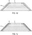
- FIG. 1(a) through FIG. 1(e) depict the process disclosed herein.
- a substrate 10 is depicted.
- the substrate 10 is shown with ridges representing a roughened surface.
- an interlayer composition 12(a) is printed or deposited on the substrate 10.
- heating step Fig. 1(c) which thermally cures the interlayer composition 12(a) to form a cured interlayer 12(b).
- a conductive ink composition 14(a) is applied to the thermally cured interlayer 12(b) shown in FIG. 1(c) .
- the part in FIG. 1(d) is then sintered to cure the conductive ink and form a solid metal trace or line 14(b) and is shown in FIG. 1(e) .
- the interlayer composition can include the following components.
- the PPGDGE is available from Sigma Aldrich and has an average molecular weight number of from about 300 to about 700.
- Propylene glycol methyl ether acetate (PGMEA) is available from Sigma Aldrich.
- Poly(4-vinyl) phenol (PVP) also available from Sigma Aldrich and has an average molecular weight from 10,000 to 40,000.
- Poly(melamine co-formaldehyde), methylated 84 weight percent solution in 1-butanol (MMF) is available from Sigma Aldrich.
- BYK®-Silclean 3700 available from BYK. Silclean is a solution of OH-functional silicone modified polyacrylate.
- BYK®-Silclean 3700 is an optional ingredient in the interlayer composition.
- BYK® 3510 surfactant also optional, can be added to the interlayer composition.
- the loading level of these surfactants is from about 0.05 weight percent to about 2 weight percent.
- the interlayer composition components are mixed to form a solution which are deposited on a substrate through aerosol printing.
- the interlayer solution in then cured in a by application of heat.
- the conductive ink is then applied and sintered to produce the final part.
- FIG. 2 shows a schematic depiction of a system 20 for printing according to embodiments disclosed herein.
- the system 20 can include a printing system 21 programmed to deposit an interlayer composition 12(a) on a substrate 10.
- the substrate 10 can be any article that can withstand the coating and curing process of the interlayer and conductive ink, for example, articles produced by a 3D printer or a printed circuit.
- the printing system 21 can be an aerosol printer, ink jet printer, spin coating printer or dip coating printer.
- the substrate 10, having the deposited interlayer composition 12(a) is then heated in a heating system 22 to the cured interlayer composition forming a solid interlayer 12(b).
- the heating system 22 can include an oven or a heated platen, such as a hotplate or a hot air gun.
- the system 20 includes a printing system 26 for depositing an ink jet composition 14(a) on the cured interlayer 12(b).
- the printing system 26 can be an aerosol printer, ink jet printer, spin coating printer or dip coating printer.
- the printing system 21 and 26 can be a single printer having different supplies for the interlayer composition and the conductive ink composition.
- the substrate 10 having the deposited conductive ink composition 14(a), is then heated in a heating system 27 to cure the conductive ink composition 14(b) forming a solid metal trace 14(b) on the cured interlayer 12(b).
- the heating system 27 can include an oven or a heated platen, such as a hotplate or a hot air gun.
- the heating systems 22 and 27 can be a single heating system.
- the system 2 can include a control system 30 coupled to the printing system 21, heating system 22, printing system 26 and/or the heating system 27.
- the control system 30 can be configured to provide instructions to, and/or otherwise control operation of the printing system 21, heating system 22, printing system 26 and/or the heating system 27.
- the control system 30 may be mechanically or electrically connected to the printing system 21, heating system 22, printing system 26 and/or the heating system 27.
- Control system 30 may be a computerized, mechanical, or electro-mechanical device capable of controlling the printing system 21, heating system 22, printing system 26 and/or the heating system 27.
- control system 30 may be a computerized device capable of providing operating instructions to the printing system 21, heating system 22, printing system 26 and/or the heating system 27.
- control system 30 may include a mechanical device, capable of use by an operator.
- the operator may physically manipulate control system 30 (e.g., by pulling a lever), which may actuate the printing system 21, heating system 22, printing system 26 and/or the heating system 27.
- control system 30 may be an electro-mechanical device.
- FIG. 3 shows a flow chart illustrating a method performed according to various embodiments.
- a magnetic stir bar was added to a 120mL amber glass bottle containing PGMEA solvent (63g) was added. Gradual addition of PMMF (5.6g) to the amber bottle while stirring at 250RPM was commenced. The mixture was stirred at 250RPM for 2 hours until the mixture was a clear solution.
- a magnetic stir bar was added to a 250mL amber glass bottle containing PGMEA solvent (63g). While stirring the PGMEA solution at 250RPM, PPGDGE polymer (52.8g) was slowly added. This mixture was stirred for 2 hours at 250RPM until all the PPGDGE was dissolved.
- the interlayer composition of Table 1 was deposited via aerosol jet printing using an Optomec Sprint System Aerosol jet printing uses nitrogen gas flowing through a specific probe geometry under pressure in a chamber (atomizer) to create aerosolized droplets containing solvent/particle mixtures which can then be focused and directed (using a sheath gas) through a small orifice (nozzle). This allows for non-contact printing by way of a fixed nozzle and moving stage. Deposition is controlled by a balance of atomizing nitrogen gas flow, focusing sheath gas and exhaust gas which regulates the vacuum source that removes un-focused streams of aerosol mixtures (typically larger atomized droplets).
- Print conditions for the interlayer composition included a nozzle size of 250 microns, a nozzle offset of 3 mm from the substrate and a line print speed of 10-25 mm/s.
- the nitrogen gas flow rates, in SCCM were: atomization nitrogen flow of 500 SCCM; exhaust nitrogen flow of 500 SCCM; and sheath gas nitrogen flow of 150 SCCM.
- Printed samples were annealed in a convection oven at 120 °C for 2 hours. Two lines of interlayer were printed side by side with a small overlap to ensure a wide enough interlayer line for printing of a conductive ink. Each line had two passes of interlayer printed to increase the height of the line and eliminate pinholes.
- Print conditions for the conductive ink included a nozzle size of 300 ⁇ m, nozzle offset of 3mm, line print speed of 5-20 mm/s, an admix (bubbler) of ethylcyclohexane was used in line with the atomization gas flow.
- the conductive ink contained from about 50 to 70 weight percent stabilized silver nanoparticles, with a blend of ethylcyclohexane and phenylcyclohexane solvents.
- the nitrogen gas flow rates for the deposition of the conductive ink were: atomization nitrogen flow of 600-800 SCCM; exhaust nitrogen flow of 600-775 SCCM; and sheath gas nitrogen flow of 50-100 SCCM.
- Printed samples were left to stand at ambient temperature for 30 minutes then annealed at 130 °C in a convection oven for 1 hour.
- the printed ink on the interlayer showed less spreading and increased line height.
- the line height was about 2.5 microns on the interlayer.
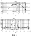
- the interlayer thickness was about 0.5 microns. This is shown in FIG. 4 .
- the interlayer is about 0.5 microns thick and is deposited on glass.
- the printed lines shown in FIG. 4 were subjected to an adhesion test. A crosshatched cut pattern of the line was created Scotch® Magic Tape (3M) was applied to the surface of the patterned line. The tape was peeled off.
- the Example with the interlayer showed no removal of the conductive ink (good adhesion). For conductive ink lines without an interlayer, adhesion was poor with all Examples showing some removal of the conductive ink layer.
- With an interlayer after removal of the tape, a thin layer of Ag was left adhering to the interlayer. The interlayer showed improved adhesion of Ag ink. Table 2 summarizes the results.
- the interlayer provides a more uniform surface for the Ag lines, which resulted in more consistent lines.
- Conductivity of the Ag lines was measured using a four point probe measurement.
Landscapes
- Chemical & Material Sciences (AREA)
- Engineering & Computer Science (AREA)
- Materials Engineering (AREA)
- Manufacturing & Machinery (AREA)
- Mechanical Engineering (AREA)
- Life Sciences & Earth Sciences (AREA)
- Wood Science & Technology (AREA)
- Organic Chemistry (AREA)
- Chemical Kinetics & Catalysis (AREA)
- Microelectronics & Electronic Packaging (AREA)
- General Chemical & Material Sciences (AREA)
- Physics & Mathematics (AREA)
- Optics & Photonics (AREA)
- Composite Materials (AREA)
- Health & Medical Sciences (AREA)
- General Health & Medical Sciences (AREA)
- Thermal Sciences (AREA)
- Toxicology (AREA)
- Dispersion Chemistry (AREA)
- Pest Control & Pesticides (AREA)
- Manufacturing Of Printed Wiring (AREA)
- Conductive Materials (AREA)
- Inks, Pencil-Leads, Or Crayons (AREA)
Abstract
Description
- The present invention relates to a multi-layer printing process. More particularly, the disclosure herein provides a method of an improved process for manufacturing printed circuits on flat and 3-dimensional (3D) surfaces.
- Solution processable conducting materials such as silver nanoparticle inks play an important role in electronic device integrations. Metal nanoparticle inks can be easily dispersed in suitable solvents and used to fabricate various conducting features in electronic devices such as electrodes and electrical interconnects by low-cost solution deposition and patterning techniques such as inkjet, aerosol, flexo and gravure printing techniques.
Flexible printed electronics are enabled by printing and annealing of silver nanoparticle inks on flexible substrates such as PET (polyethylene terephthalate) and polyimide. However, many silver nanoparticle inks suffer from poor adhesion on such substrates, which limits the opportunities for robust device fabrication. Addition of polymeric materials directly to the conductive ink is usually not possible, as this results in decreased conductivity of the final conductive metal trace that is formed. It would be desirable to have processes that improve conductive ink adhesion and enable formation of printed electronic devices with robust mechanical properties without sacrificing electric conductivity. - According to an embodiment, there is provided a printing method which includes providing a substrate and depositing an interlayer composition including a polymer selected from the group of epoxy resins, polyvinyl phenols and poly(melamine-co-formaldehyde) and an interlayer composition solvent on the substrate. The interlayer composition is cured to form cured interlayer. A conductive metal ink composition is deposited on the cured interlayer and the conductive metal ink composition is cured to form a solid metal trace on the cured interlayer.
- According to an embodiment, there is provided a printing system. The printing system includes an interlayer printer system that deposits an interlayer composition a polymer selected from the group of epoxy resins, polyvinyl phenols and poly(melamine-co-formaldehyde) and an interlayer composition solvent on a substrate. The printing system includes a heating system for curing the interlayer composition on a surface of the substrate to form a cured interlayer. The printing system includes a conductive ink printer system for depositing a conductive metal ink composition on the cured interlayer. The printing system includes a heater system for curing the conductive ink composition to form a trace on the cured interlayer.
- According to another embodiment there is provided a printing method including depositing an interlayer composition including a polymer selected from the group of epoxy resins, polyvinyl phenols and poly(melamine-co-formaldehyde) and an interlayer composition solvent on a substrate. The printing method includes curing the interlayer composition to form a cured interlayer. A conductive metal ink composition is deposited on the cured interlayer. The conductive metal ink composition includes silver nanoparticles having a size of from about 0.5 to about 100 nm. The conductive metal ink composition to form a solid metal trace on the cured interlayer.
- The accompanying drawings, which are incorporated in and constitute a part of this specification, illustrate several embodiments of the present teachings and together with the description, serve to explain the principles of the present teachings.
-
FIGS. 1 (a)-(e) illustrate processes in a method for printing according to embodiments of the invention. -
FIG. 2 shows a schematic depiction of a printing system for various embodiments disclosed herein. -
FIG. 3 shows a flow chart illustrating a method according to various embodiments disclosed herein. -
FIG. 4 illustrates the height and width profile of conductive line printer on an interlayer composition disclosed herein. - It should be noted that some details of the FIGS. have been simplified and are drawn to facilitate understanding of the embodiments rather than to maintain strict structural accuracy, detail, and scale.
- Reference will now be made in detail to embodiments of the present teachings, examples of which are illustrated in the accompanying drawings. Wherever possible, the same reference numbers will be used throughout the drawings to refer to the same or like parts.
- In the following description, reference is made to the accompanying drawings that form a part thereof, and in which is shown by way of illustration specific exemplary embodiments in which the present teachings may be practiced. These embodiments are described in sufficient detail to enable those skilled in the art to practice the present teachings and it is to be understood that other embodiments may be utilized and that changes may be made without departing from the scope of the present teachings. The following description is, therefore, merely illustrative.
- Illustrations with respect to one or more implementations, alterations and/or modifications can be made to the illustrated examples without departing from the spirit and scope of the appended claims. In addition, while a particular feature may have been disclosed with respect to only one of several implementations, such feature may be combined with one or more other features of the other implementations as may be desired and advantageous for any given or particular function. Furthermore, to the extent that the terms "including", "includes", "having", "has", "with", or variants thereof are used in either the detailed description and the claims, such terms are intended to be inclusive in a manner similar to the term "comprising." The term "at least one of" is used to mean one or more of the listed items can be selected.
- Notwithstanding that the numerical ranges and parameters setting forth the broad scope of embodiments are approximations, the numerical values set forth in the specific examples are reported as precisely as possible. Any numerical value, however, inherently contains certain errors necessarily resulting from the standard deviation found in their respective testing measurements. Moreover, all ranges disclosed herein are to be understood to encompass any and all sub-ranges subsumed therein. For example, a range of "less than 10" can include any and all sub-ranges between (and including) the minimum value of zero and the maximum value of 10, that is, any and all sub-ranges having a minimum value of equal to or greater than zero and a maximum value of equal to or less than 10, e.g., 1 to 5. In certain cases, the numerical values as stated for the parameter can take on negative values. In this case, the example value of range stated as "less than 10" can assume negative values, e.g. - 1, -2, -3, -10, -20, -30, etc.
- Metal nanoparticle inks, including silver inks play an important role in electronic device integrations. One issue often encountered is poor adhesion. The sintered metal nanoparticle inks do not have good adhesion on certain substrates, especially glass. Previously, this adhesion issue was addressed by addition of small amount of polymeric materials in metal nanoparticle inks. The disadvantage of this approach is the sacrifice of electrical conductivity. Disclosed herein is an improved process for enhancing adhesion without sacrificing electrical conductivity of the metal nanoparticle inks used in electronic device applications.
- Disclosed herein is a printing process for depositing a reactive thermally curable interlayer composition which improves the adhesion and can create a smooth surface between substrates and printed conductive ink.
- Specifically, the disclosed process uses aerosol printing of a thermally curable interlayer composition. Additives can optionally be included in the interlayer composition to improve wetting and spreading properties. The interlayer can be fabricated by solution process methods including spin coating, dip coating, and inkjet printing etc. on various substrates, followed by heat treatment for curing. The interlayer provides good adhesion on a variety of substrates. Conductive features can be fabricated by solution processing techniques such as ink jet or aerosol printing onto the substrates with the applied and cured interlayer.
- The process disclosed herein deposits an interlayer composition on a surface of a substrate prior to the coating the conductive ink. The substrate can be any article that can withstand the coating and curing process of the interlayer and conductive ink, for example articles produced by a 3D printer or a printed circuit. The interlayer provides improved adhesion of the conductive ink to the substrate. The interlayer lowers the surface roughness of the substrate that is being coated with conductive ink.
- Many 3D printed parts have a roughened surface, by virtue of the printing process used to make the part. For example, FDM (fused deposition modelling) leaves signature 'corduroy' textured surfaces as a function of the layer-by-layer deposition of molten filament. MJM (multi-jet modelling) can have rough surfaces due to the co-printed support material which is later removed (usually by mechanical/thermal methods). This can leave a roughened interface. SLS (selective laser sintering) can also leave a pitted/roughened surface as well.
- FDM uses thermoplastic materials such as polylactic acid (PLA), acrylonitrile butadiene styrene (ABS), nylon, polyetherimide and acrylonitrile styrene acrylate (ASA). FDM 3D printing uses filaments that are unwound from a coil and supplied to an extrusion nozzle. The flow is turned on and off to deposit the material in the proper place. The nozzle is heated to melt the material. The thermoplastics are heated past their glass transition temperature and are deposited by an extrusion head. The nozzle can be moved in both horizontal and vertical directions by a numerically controlled mechanism. The nozzle follows a tool-path controlled by a computer-aided manufacturing (CAM) software package, and the part is built from the bottom up, one layer at a time.
- MJM is an inkjet printing process that uses piezo printhead technology to deposit either photocurable plastics layer by layer. Materials include UV curable materials such as acrylates and methacrylates.
- SLS is an additive manufacturing technique that uses a high power laser to fuse small particles together. Material options include plastic, metal, ceramic, nylon, polystyrene or glass powder. In many cases, SLS does not require any support structures, as parts are surrounded by unsintered powder at all times.
- By applying an interlayer composition to the surface of a substrate improvements in smoothness, adhesion and conductivity are achieved.
- The interlayer composition can include epoxy resins, polyvinyl phenols and poly(melamine-co-formaldehyde). The poly(melamine-co-formaldehyde) can be methylated, butylated, isobutylated or acrylated. The interlayer composition may further contain small amounts of a surface levelling agent to control wetting and spreading properties of coating as well as catalyst for curing process.
- The interlayer composition can optionally include a catalyst. Any suitable or desired catalyst can be selected for the present interlayer compositions. In embodiments, the catalyst is selected from the group consisting of amine salts of dodecylbenzene sulfonic acid (DDBSA), para toluene sulfonic acid, triflouromethane sulfonic acid, and combinations thereof.
- The catalyst can be provided in the interlayer composition in any suitable or desired amount. In embodiments, the catalyst is present in an amount of from about 0.05 to about 1.5 percent, or from about 0.08 to about 1.0 percent, or from about 0.1 to about 0.5 percent, by weight, based on the total weight of the interlayer composition.
- The interlayer composition includes a solvent. The solids content of the interlayer composition is from about 10 weight percent to about 50 weight percent, or from about 20 weight percent to about 40 weight percent or from about 30 weight percent to about 40 weight percent. Many solvents are suitable for the interlayer composition. The solvent can be a nonpolar organic solvent selected from the group consisting of hydrocarbons such as alkanes, alkenes, alcohols having from about 7 to about 18 carbon atoms such as undecane, dodecane, tridecane, tetradecane, hexadecane, 1-undecanol, 2-undecanol, 3-undecanol, 4-undecanol, 5-undecanol, 6-undecanol, 1-dodecanol, 2-dodecanol, 3-dedecanol, 4-dedecanol, 5-dodecanol, 6-dodecanol, 1-tridecanol, 2-tridecanol, 3-tridecanol, 4-tridecanol, 5-tridecanol, 6-tridecanol, 7-tridecanol, 1-tetradecanol, 2-tetradecanol, 3-tetradecanol, 4-tetradecanol, 5-tetradecanol, 6-tetradecanol, 7-tetradecanol, and the like; alcohols such as terpineol (α-terpineol), β-terpineol, geraniol, cineol, cedral, linalool, 4-terpineol, 3,7-dimethylocta-2,6-dien-lol, 2-(2-propyl)-5-methyl-cyclohexane-1-ol; isoparaffinic hydrocarbons such as isodecane, isododecane; commercially available mixtures of isoparaffins such as Isopar™ E, Isopar™ G, Isopar™ H, Isopar™ L, Isopar™ V, Isopar™ G, manufactured by Exxon Chemical Company; Shellsol® manufactured by Shell Chemical Company; Soltrol® manufactured by Chevron Phillips Chemical Company; Begasol® manufactured by Mobil Petroleum Co., Inc.; IP Solvent 2835 manufactured by Idemitsu Petrochemical CO., Ltd; naphthenic oils; aromatic solvents such as benzene, nitrobenzene, toluene, ortho-, meta-, and para-xylene, and mixtures thereof; 1,3,5-trimethylbenzene (mesitylene); 1,2-, 1,3-, and 1,4-dichlorobenzene and mixtures thereof, trichlorobenzene; cyanobenzene; phenylcyclohexane and tetralin; aliphatic solvents such as isooctane, nonane, decane, dodecane; cyclic aliphatic solvents such as dicyclohexyl and decalin; and mixtures and combinations thereof. In embodiments, two or more solvents can be used.
- The solvent can be provided in the interlayer composition in any suitable or desired amount. In embodiments, the solvent is present in an amount of from about 50 to about 90 percent, or from about 60 to about 80 percent, or from about 70 to about 80 percent, by weight, based on the total weight of the interlayer composition.
- The interlayer composition is stable and can be coated and cured at temperatures ranging from about 100°C to about 180°C. Since epoxy resins are excellent electrical insulators, the electrical conductivity of metal nanoparticle inks will not be affected by this interlayer coating.
- The interlayer solution is very stable and coating can be cured at low temperature. Since epoxy resins are excellent electrical insulators, the electrical conductivity of metal nanoparticle inks will not be affected by this interlayer coating.
- The interlayer solution can be deposited by aerosol printing and then thermally cured. The interlayer composition can be deposited by solution processing methods including spin coating, dip coating, and inkjet printing etc. on various substrates and curing at suitable temperatures and times.
- After application and curing of the interlayer, the conductive ink is applied to the cured interlayer.
- The conductive inks may be made include dissolved or stabilized metal nanoparticles in a solvent. The conductive inks are deposited on the cured interlayer. The deposition of the conductive ink on a cured interlayer on the substrate is through any suitable printing technique, for example, aerosol printing, spin coating, dip coating and inkjet printing. In an aerosol printing process, an ultrasonic transducer device is used to create a fine aerosol mist of ink droplets that is pumped through a nozzle.
- According to embodiments herein, the nanoparticles in the conductive inks may have diameter in the submicron range. Silver, gold and copper are suitable metals for the conductive inks. Silver nanoparticles sinter at 120°C which is more than 800°C below the melting temperature of bulk silver. Copper and gold nanoparticles have comparable melting points of between 100°C and 140°C, whereas the melting temperatures for bulk gold or copper is in the range of 1060°C to 1085°C. This lower melting point is a result of comparatively high surface-area-to-volume ratio in nanoparticles, which allows bonds to readily form between neighboring particles. The large reduction in sintering temperature for nanoparticles enables forming highly conductive traces or patterns on the interlayer, because the interlayer choice melt or soften at relatively low temperatures (for example, 150°C). 20. The conductive metal ink composition is cured at a temperature of from about 100°C to about 180°C.
- In embodiments, the metal nanoparticles may be elemental silver, gold or copper, a alloys of silver gold or copper or combinations thereof. In embodiments, the metal nanoparticles may be a base material coated or plated with pure silver or a silver alloy. For example, the base material may be copper flakes with silver plating.
- In embodiments, the silver may include either or both of (i) one or more other metals and (ii) one or more non-metals. Suitable other metals include, for example, Al, Au, Pt, Pd, Cu, Co, Cr, In, and Ni, particularly the transition metals, for example, Au, Pt, Pd, Cu, Cr, Ni, and mixtures thereof. Exemplary metal composites includes Au--Ag, Ag--Cu, Au--Ag--Cu, and Au-Ag--Pd. Suitable non-metals in the metal composite include, for example, Si, C, and Ge.
- The nanoparticles for the conductive ink may have an average particle size, for example, from about 0.5 to about 100 nm, or from about 1.0 to about 50.0 microns, or from about 1.0 to about 20.0 microns.
- The metal nanoparticles may be present in the conductive ink in an amount, for example, at least about 50 weight percent of the conductive ink, or from about 50 to about 90 weight percent of the conductive ink, or from about 55 to about 85 weight percent of the conductive ink.
- The conductive ink may include a solvent(s). The solvent(s) may be used as a vehicle for dispersion of the metal nanoparticles to minimize or prevent the metal nanoparticles from agglomerating and/or optionally providing or enhancing the solubility or dispersiblity of metal nanoparticles.
- In embodiments, a viscosity (less than 5 cps) and high metal loading (greater than 50 weight percent) are suitable for printing. Solvent(s) used in the conductive ink herein may have a viscosity equal to or less than about 1 cps. In addition, the solvent(s) can have good miscibility with the metal nanoparticles.
- Any suitable solvent(s) having a viscosity equal to or less than about 1 cps may be used to dissolve or to disperse the silver nanoparticle for the ink herein. Examples of suitable solvents may include organic solvents, for example, a hydrocarbon, a heteroatom-containing aromatic compound, or an alcohol. Suitable organic solvent(s) herein may be, for example, decalin, bicyclohexyl, ethylcyclohexane, phenylcyclohexane, tetralin, cyclohexane, n-octane, toluene, m-xylene, o-xylene, p-xylene, mesitylene, isopar, heptane, isooctane, and trimethylbenzene. These types of solvents have very low viscosity property (equal to or less than about 1 cps) and good solubility for silver nanoparticles.
- The solvent may be present in the conductive ink in an amount, for example, from about 2.0 to about 50.0 weight percent of the conductive ink, or from about 5.0 to about 40.0 weight percent of the conductive ink, or from about 10.0 to about 30.0 weight percent of the conductive ink.
- Following printing of the nanoparticle ink on the interlayer, the ink is subjected to a curing step. The curing step removes substantially all of the solvent and the organic stabilizer, and the destabilized particles weld together (sinter) to form a continuous metal film that firmly adheres to the interlayer.
-
FIG. 1(a) through FIG. 1(e) depict the process disclosed herein. InFIG. 1(a) , asubstrate 10 is depicted. Thesubstrate 10 is shown with ridges representing a roughened surface. InFIG. 1(b) , an interlayer composition 12(a) is printed or deposited on thesubstrate 10. After deposition of the interlayer 12(a), there is heating step (Fig. 1(c) which thermally cures the interlayer composition 12(a) to form a cured interlayer 12(b). InFIG. 1(d) a conductive ink composition 14(a) is applied to the thermally cured interlayer 12(b) shown inFIG. 1(c) . The part inFIG. 1(d) is then sintered to cure the conductive ink and form a solid metal trace or line 14(b) and is shown inFIG. 1(e) . - The interlayer composition can include the following components. Poly(propylene glycol) diglycidyl ether (PPGDGE). The PPGDGE is available from Sigma Aldrich and has an average molecular weight number of from about 300 to about 700. Propylene glycol methyl ether acetate (PGMEA) is available from Sigma Aldrich. Poly(4-vinyl) phenol (PVP) also available from Sigma Aldrich and has an average molecular weight from 10,000 to 40,000. Poly(melamine co-formaldehyde), methylated 84 weight percent solution in 1-butanol (MMF) is available from Sigma Aldrich. BYK®-Silclean 3700 available from BYK. Silclean is a solution of OH-functional silicone modified polyacrylate. BYK®-Silclean 3700 is an optional ingredient in the interlayer composition. BYK® 3510 surfactant, also optional, can be added to the interlayer composition. The loading level of these surfactants is from about 0.05 weight percent to about 2 weight percent. The interlayer composition components are mixed to form a solution which are deposited on a substrate through aerosol printing. The interlayer solution in then cured in a by application of heat. The conductive ink is then applied and sintered to produce the final part.
-
FIG. 2 shows a schematic depiction of asystem 20 for printing according to embodiments disclosed herein. As shown, thesystem 20 can include aprinting system 21 programmed to deposit an interlayer composition 12(a) on asubstrate 10. Thesubstrate 10 can be any article that can withstand the coating and curing process of the interlayer and conductive ink, for example, articles produced by a 3D printer or a printed circuit. Theprinting system 21 can be an aerosol printer, ink jet printer, spin coating printer or dip coating printer. - The
substrate 10, having the deposited interlayer composition 12(a) is then heated in aheating system 22 to the cured interlayer composition forming a solid interlayer 12(b). Theheating system 22 can include an oven or a heated platen, such as a hotplate or a hot air gun. - The
system 20 includes aprinting system 26 for depositing an ink jet composition 14(a) on the cured interlayer 12(b). Theprinting system 26 can be an aerosol printer, ink jet printer, spin coating printer or dip coating printer. Theprinting system - The
substrate 10 having the deposited conductive ink composition 14(a), is then heated in aheating system 27 to cure the conductive ink composition 14(b) forming a solid metal trace 14(b) on the cured interlayer 12(b). Theheating system 27 can include an oven or a heated platen, such as a hotplate or a hot air gun. Theheating systems - In various embodiments, the system 2 can include a
control system 30 coupled to theprinting system 21,heating system 22,printing system 26 and/or theheating system 27. Thecontrol system 30 can be configured to provide instructions to, and/or otherwise control operation of theprinting system 21,heating system 22,printing system 26 and/or theheating system 27. Thecontrol system 30 may be mechanically or electrically connected to theprinting system 21,heating system 22,printing system 26 and/or theheating system 27.Control system 30 may be a computerized, mechanical, or electro-mechanical device capable of controlling theprinting system 21,heating system 22,printing system 26 and/or theheating system 27. In one embodiment,control system 30 may be a computerized device capable of providing operating instructions to theprinting system 21,heating system 22,printing system 26 and/or theheating system 27. In another embodiment,control system 30 may include a mechanical device, capable of use by an operator. In this case, the operator may physically manipulate control system 30 (e.g., by pulling a lever), which may actuate theprinting system 21,heating system 22,printing system 26 and/or theheating system 27. In another embodiment,control system 30 may be an electro-mechanical device. -
FIG. 3 shows a flow chart illustrating a method performed according to various embodiments. - Process P1: An interlayer composition is coated on a substrate. The interlayer composition includes thermally curable polymer such as epoxy, polyvinyl phenol and poly(melamine-co-formaldehyde). The interlayer includes a solvent and an optional levelling agent or surfactant and a catalyst.
- Process P2: The interlayer composition is cured by heating. The heating evaporates the solvents and cures the thermally curable polymer to form a smooth surface.
- Process P3: A conductive ink composition is coated on the cured interlayer. The conductive ink composition includes metal nanoparticles and a solvent and an organic stabilizer.
- Process P4: The conductive ink composition is heated to remove the solvent sinter the metal nanoparticles to form a solid trace on the cured interlayer.
- A magnetic stir bar was added to a 120mL amber glass bottle containing PGMEA solvent (63g) was added. Gradual addition of PMMF (5.6g) to the amber bottle while stirring at 250RPM was commenced. The mixture was stirred at 250RPM for 2 hours until the mixture was a clear solution.
- A magnetic stir bar was added to a 250mL amber glass bottle containing PGMEA solvent (63g). While stirring the PGMEA solution at 250RPM, PPGDGE polymer (52.8g) was slowly added. This mixture was stirred for 2 hours at 250RPM until all the PPGDGE was dissolved.
- The 120mL bottle containing PMMF/PGMEA was poured into the 250mL bottle containing PLDGE/PGMEA, while stirring at 250RPM. PVP (10g) was slowly added to the mixture with stirring until the PVP was completely dissolved. The bottle was placed on a Movil-rod mixer to gently tumble and roll the final mixture overnight at 175RPM. Finally, the solution was filtered through 0.2 micron filter paper to remove any suspended matter, resulting in a clear, colorless solution. Table 1 shows the weight percent of the components of the interlayer composition.
Table 1: Interlayer formulation composition Sample ID PPGDGE Mn 389 (wt%) PMMF (wt%) PVP (wt%) PGMEA Solvent (wt%) % solids TOTAL (wt%) EXP-AA0736-37 26.45 5.60 4.95 63.00 37.00 100.00 - The interlayer composition of Table 1 was deposited via aerosol jet printing using an Optomec Sprint System Aerosol jet printing uses nitrogen gas flowing through a specific probe geometry under pressure in a chamber (atomizer) to create aerosolized droplets containing solvent/particle mixtures which can then be focused and directed (using a sheath gas) through a small orifice (nozzle). This allows for non-contact printing by way of a fixed nozzle and moving stage. Deposition is controlled by a balance of atomizing nitrogen gas flow, focusing sheath gas and exhaust gas which regulates the vacuum source that removes un-focused streams of aerosol mixtures (typically larger atomized droplets). Print conditions for the interlayer composition included a nozzle size of 250 microns, a nozzle offset of 3 mm from the substrate and a line print speed of 10-25 mm/s. The nitrogen gas flow rates, in SCCM (standard cubic centimeters per minute) were: atomization nitrogen flow of 500 SCCM; exhaust nitrogen flow of 500 SCCM; and sheath gas nitrogen flow of 150 SCCM. Printed samples were annealed in a convection oven at 120 °C for 2 hours. Two lines of interlayer were printed side by side with a small overlap to ensure a wide enough interlayer line for printing of a conductive ink. Each line had two passes of interlayer printed to increase the height of the line and eliminate pinholes.
- Print conditions for the conductive ink included a nozzle size of 300 µm, nozzle offset of 3mm, line print speed of 5-20 mm/s, an admix (bubbler) of ethylcyclohexane was used in line with the atomization gas flow. The conductive ink contained from about 50 to 70 weight percent stabilized silver nanoparticles, with a blend of ethylcyclohexane and phenylcyclohexane solvents. The nitrogen gas flow rates for the deposition of the conductive ink were: atomization nitrogen flow of 600-800 SCCM; exhaust nitrogen flow of 600-775 SCCM; and sheath gas nitrogen flow of 50-100 SCCM. Printed samples were left to stand at ambient temperature for 30 minutes then annealed at 130 °C in a convection oven for 1 hour.
- The printed ink on the interlayer showed less spreading and increased line height. The line height was about 2.5 microns on the interlayer. The interlayer thickness was about 0.5 microns. This is shown in
FIG. 4 . InFIG. 4 , the interlayer is about 0.5 microns thick and is deposited on glass.
The printed lines shown inFIG. 4 were subjected to an adhesion test. A crosshatched cut pattern of the line was created Scotch® Magic Tape (3M) was applied to the surface of the patterned line. The tape was peeled off. The Example with the interlayer showed no removal of the conductive ink (good adhesion). For conductive ink lines without an interlayer, adhesion was poor with all Examples showing some removal of the conductive ink layer. With an interlayer, after removal of the tape, a thin layer of Ag was left adhering to the interlayer. The interlayer showed improved adhesion of Ag ink. Table 2 summarizes the results. -
Table 2: Adhesion Tape Test Results Substrate Material Being Tested Adhesion score (0-5) Scotch tape test Notes PET (Flex) Interlayer 5 PET (Flex) Ag 0-3 (average 1) PET (Flex) with interlayer Ag 0 Conductive layer adheres to interlayer Glass Interlayer 5 Glass Ag 0 Glass with interlayer Ag 0 Conductive layer adheres to interlayer PEN (Flex) Interlayer 5 PEN (Flex) Ag 3 PEN (Flex) with interlayer Ag 0-3 (average 1) Conductive layer adheres to interlayer PC (Flex) Interlayer 5 PC (Flex) Ag 0-2 (average 1.125) PC (rigid) Interlayer 5 PC (rigid) Ag 0 PC (rigid) with interlayer Ag 0-2 (average 1.125) Conductive layer adheres to interlayer, but poor cohesion - The interlayer provides a more uniform surface for the Ag lines, which resulted in more consistent lines.
- Conductivity of the Ag lines was measured using a four point probe measurement.
- It will be appreciated that variants of the above-disclosed and other features and functions or alternatives thereof may be combined into other different systems or applications. Various presently unforeseen or unanticipated alternatives, modifications, variations, or improvements therein may be subsequently made by those skilled in the art, which are also encompassed by the following claims.
Claims (10)
- A printing method comprising:depositing an interlayer composition including a polymer selected from the group of consisting of: epoxy resins, polyvinyl phenols and poly(melamine-co-formaldehyde) and an interlayer composition solvent on a substrate;curing the interlayer composition to form a cured interlayer;depositing a conductive metal ink composition on the cured interlayer; andcuring the conductive metal ink composition to form a solid metal trace on the cured interlayer.
- The printing method according to claim 1, wherein the interlayer composition solvent is selected from the group consisting of: hydrocarbons, alcohols having from about 7 to about 18 carbon atoms, terpineol (α-terpineol), β-terpineol, geraniol, cineol, cedral, linalool, 4-terpineol, 3,7-dimethylocta-2,6-dien-1 ol, 2-(2-propyl)-5-methyl-cyclohexane-1-ol, isoparaffinic hydrocarbons, isoparaffins, naphthenic oils, benzene, nitrobenzene, toluene, ortho-xylene, metaxylene, para-xylene, 1,3,5-trimethylbenzene, 1,2- dichlorobenzene, 1,3- dichlorobenzene, 1,4-dichlorobenzene, trichlorobenzene; cyanobenzene; phenylcyclohexane, tetralin, isooctane, nonane, decane, dodecane, dicyclohexyl and decalin.
- The printing method according to claim 1, wherein the substrate comprises a material selected from the group consisting of: polyactic acid, acrylonitrile butadiene styrene (ABS), nylon, polyetherimide, acrylonitrile styrene acrylate, plastic, metal, ceramic, nylon, polystyrene, glass powder and UV curable plastic.
- The printing method according to claim 1, wherein the conductive ink composition comprises silver nanoparticles and solvent.
- A printing system comprising:an interlayer printer system depositing an interlayer composition including a polymer selected from the group of epoxy resins, polyvinyl phenols and poly(melamine-co-formaldehyde) and an interlayer composition solvent on a substrate;a heating system for curing the interlayer composition on a surface of the substrate to form a cured interlayer; anda conductive ink printer system for depositing a conductive metal ink composition on the cured interlayer; anda heater system for curing the conductive ink composition to form a trace on the cured interlayer.
- The printing system according to claim 5, wherein the interlayer composition solvent is selected from the group consisting of: hydrocarbons, alcohols having from about 7 to about 18 carbon atoms, terpineol (α-terpineol), β-terpineol, geraniol, cineol, cedral, linalool, 4-terpineol, 3,7-dimethylocta-2,6-dien-1ol, 2-(2-propyl)-5-methyl-cyclohexane-1-ol, isoparaffinic hydrocarbons, isoparaffins, naphthenic oils, benzene, nitrobenzene, toluene, ortho-xylene, metaxylene, para-xylene, 1,3,5-trimethylbenzene, 1,2- dichlorobenzene, 1,3- dichlorobenzene, 1,4-dichlorobenzene, trichlorobenzene; cyanobenzene; phenylcyclohexane, tetralin, isooctane, nonane, decane, dodecane, dicyclohexyl and decalin.
- The printing system according to claim 5, wherein the substrate comprises a material selected from the group consisting of: polyactic acid, acrylonitrile butadiene styrene (ABS), nylon, polyetherimide, acrylonitrile styrene acrylate, plastic, metal, ceramic, nylon, polystyrene, glass powder and UV curable plastic.
- A printing method comprising:depositing an interlayer composition including a polymer selected from the group of epoxy resins, polyvinyl phenols and poly(melamine-co-formaldehyde) and an interlayer composition solvent on a substrate;curing the interlayer composition to form a cured interlayer;depositing a conductive metal ink composition on the cured interlayer, the conductive metal ink composition comprising silver nanoparticles having a size of from about 0.5 to about 100 nm; andcuring the conductive metal ink composition to form a solid metal trace on the cured interlayer.
- The printing method according to claim 8, wherein the ink composition solvent is selected from the group consisting of: decalin, bicyclohexyl, ethylcyclohexane, phenylcyclohexane, tetralin, cyclohexane, n-octane, toluene, m-xylene, o-xylene, p-xylene, mesitylene, isopar, heptane, isooctane, and trimethylbenzene.
- The printing method according to claim 8, wherein the interlayer composition is cured at a temperature of from about 100°C to about 180°C.
Applications Claiming Priority (1)
| Application Number | Priority Date | Filing Date | Title |
|---|---|---|---|
| US15/414,814 US10899940B2 (en) | 2017-01-25 | 2017-01-25 | Interlayer printing process |
Publications (2)
| Publication Number | Publication Date |
|---|---|
| EP3355668A1 true EP3355668A1 (en) | 2018-08-01 |
| EP3355668B1 EP3355668B1 (en) | 2022-12-14 |
Family
ID=60990658
Family Applications (1)
| Application Number | Title | Priority Date | Filing Date |
|---|---|---|---|
| EP18151219.5A Active EP3355668B1 (en) | 2017-01-25 | 2018-01-11 | Interlayer printing process |
Country Status (5)
| Country | Link |
|---|---|
| US (1) | US10899940B2 (en) |
| EP (1) | EP3355668B1 (en) |
| JP (1) | JP6921763B2 (en) |
| KR (1) | KR102279969B1 (en) |
| CA (1) | CA2992226C (en) |
Cited By (1)
| Publication number | Priority date | Publication date | Assignee | Title |
|---|---|---|---|---|
| US10899940B2 (en) | 2017-01-25 | 2021-01-26 | Xerox Corporation | Interlayer printing process |
Families Citing this family (13)
| Publication number | Priority date | Publication date | Assignee | Title |
|---|---|---|---|---|
| KR102190291B1 (en) * | 2017-04-28 | 2020-12-14 | 한국전기연구원 | Ag Ink For 3D Printing And 3D Printing Methods Using The Same |
| US10821658B2 (en) * | 2018-07-24 | 2020-11-03 | Xerox Corporation | Conductive three-dimensional articles |
| US10947424B2 (en) * | 2018-08-02 | 2021-03-16 | Xerox Corporation | Adhesive composition comprising eutectic metal alloy nanoparticles |
| US11142671B2 (en) * | 2018-08-02 | 2021-10-12 | Xerox Corporation | Adhesive composition comprising metal nanoparticles |
| US11426818B2 (en) | 2018-08-10 | 2022-08-30 | The Research Foundation for the State University | Additive manufacturing processes and additively manufactured products |
| WO2020048889A1 (en) | 2018-09-03 | 2020-03-12 | Signify Holding B.V. | Printing method for fdm printing smooth surfaces of items |
| WO2020055429A1 (en) * | 2018-09-14 | 2020-03-19 | Hewlett-Packard Development Company, L.P. | Three-dimensional printing |
| US10926460B2 (en) * | 2018-09-28 | 2021-02-23 | The Boeing Company | Methods and apparatus for additively manufacturing a structure with in-situ reinforcement |
| US10926461B2 (en) * | 2018-09-28 | 2021-02-23 | The Boeing Company | Methods and apparatus for additively manufacturing a structure with in-situ reinforcement |
| US10926325B2 (en) * | 2018-09-28 | 2021-02-23 | The Boeing Company | Methods and apparatus for additively manufacturing a structure with in-situ reinforcement |
| WO2020123308A1 (en) * | 2018-12-14 | 2020-06-18 | Yazaki Corporation | Additive manufacturing techniques for producing a network of conductive pathways on a substrate |
| CN114206593A (en) * | 2019-08-09 | 2022-03-18 | 美国圣戈班性能塑料公司 | Additive Manufacturing Components and Methods |
| DE102023102354A1 (en) * | 2023-01-31 | 2024-08-01 | additive electronics GmbH | Device for producing three-dimensional electronic components |
Citations (3)
| Publication number | Priority date | Publication date | Assignee | Title |
|---|---|---|---|---|
| US20110111588A1 (en) * | 2008-06-30 | 2011-05-12 | Konica Minolta Holdings, Inc. | Wiring forming method |
| US20120168211A1 (en) * | 2010-12-30 | 2012-07-05 | Industrial Technology Research Institute | Substrate assembly containing conductive film and fabrication method thereof |
| US20160204494A1 (en) * | 2015-01-08 | 2016-07-14 | Microsoft Technology Licensing, Llc | 3d multilayer high frequency signal line |
Family Cites Families (12)
| Publication number | Priority date | Publication date | Assignee | Title |
|---|---|---|---|---|
| EP1139705B1 (en) | 1999-09-02 | 2006-11-22 | Ibiden Co., Ltd. | Printed wiring board and method of producing the same |
| US6461717B1 (en) * | 2000-04-24 | 2002-10-08 | Shipley Company, L.L.C. | Aperture fill |
| JP2002072519A (en) * | 2000-09-04 | 2002-03-12 | Sharp Corp | Coating solution for charge generation layer, organic electrophotographic photoreceptor, and method for producing the same |
| GB0511132D0 (en) * | 2005-06-01 | 2005-07-06 | Plastic Logic Ltd | Layer-selective laser ablation patterning |
| JP4874719B2 (en) * | 2006-06-19 | 2012-02-15 | 富士フイルム株式会社 | Ink composition, inkjet recording method, lithographic printing plate production method, and lithographic printing plate |
| JP2008006779A (en) * | 2006-06-30 | 2008-01-17 | Daido Kasei Kogyo Kk | Composition for active energy beam curable type ink jet recording material coating, and ink jet recording material |
| WO2014156844A1 (en) * | 2013-03-29 | 2014-10-02 | 太陽ホールディングス株式会社 | Thermoplastic resin film base for optical firing, conductive circuit board using same, and method for manufacturing said conductive circuit board |
| CN104250422A (en) * | 2013-06-26 | 2014-12-31 | 合肥杰事杰新材料股份有限公司 | Photosensitive resin used in 3D printing, and its preparation method |
| JP6349813B2 (en) * | 2014-03-17 | 2018-07-04 | 株式会社リコー | Droplet ejection apparatus, image forming apparatus, and droplet ejection head control method |
| JP6180975B2 (en) * | 2014-03-19 | 2017-08-16 | 株式会社東芝 | Electronic device and manufacturing method thereof |
| CN104448715A (en) * | 2014-12-29 | 2015-03-25 | 大连理工常熟研究院有限公司 | Photo-curing material for injection type 3D printer |
| US10899940B2 (en) | 2017-01-25 | 2021-01-26 | Xerox Corporation | Interlayer printing process |
-
2017
- 2017-01-25 US US15/414,814 patent/US10899940B2/en active Active
-
2018
- 2018-01-10 KR KR1020180003385A patent/KR102279969B1/en active Active
- 2018-01-10 JP JP2018001773A patent/JP6921763B2/en active Active
- 2018-01-11 EP EP18151219.5A patent/EP3355668B1/en active Active
- 2018-01-18 CA CA2992226A patent/CA2992226C/en active Active
Patent Citations (3)
| Publication number | Priority date | Publication date | Assignee | Title |
|---|---|---|---|---|
| US20110111588A1 (en) * | 2008-06-30 | 2011-05-12 | Konica Minolta Holdings, Inc. | Wiring forming method |
| US20120168211A1 (en) * | 2010-12-30 | 2012-07-05 | Industrial Technology Research Institute | Substrate assembly containing conductive film and fabrication method thereof |
| US20160204494A1 (en) * | 2015-01-08 | 2016-07-14 | Microsoft Technology Licensing, Llc | 3d multilayer high frequency signal line |
Cited By (1)
| Publication number | Priority date | Publication date | Assignee | Title |
|---|---|---|---|---|
| US10899940B2 (en) | 2017-01-25 | 2021-01-26 | Xerox Corporation | Interlayer printing process |
Also Published As
| Publication number | Publication date |
|---|---|
| US20180208785A1 (en) | 2018-07-26 |
| JP2018121052A (en) | 2018-08-02 |
| CA2992226C (en) | 2021-06-01 |
| KR20180087839A (en) | 2018-08-02 |
| CA2992226A1 (en) | 2018-07-25 |
| JP6921763B2 (en) | 2021-08-18 |
| US10899940B2 (en) | 2021-01-26 |
| KR102279969B1 (en) | 2021-07-22 |
| EP3355668B1 (en) | 2022-12-14 |
Similar Documents
| Publication | Publication Date | Title |
|---|---|---|
| EP3355668B1 (en) | Interlayer printing process | |
| JP5650054B2 (en) | Silver nanoparticle composition comprising a solvent having specific Hansen solubility parameters | |
| JP7212591B2 (en) | Adhesive composition containing metal nanoparticles | |
| Wu et al. | Inkjet printing of low-temperature cured silver patterns by using AgNO3/1-dimethylamino-2-propanol inks on polymer substrates | |
| JP7212593B2 (en) | Adhesive composition containing eutectic metal alloy nanoparticles | |
| Hou et al. | Three dimensional printed electronic devices realised by selective laser melting of copper/high-density-polyethylene powder mixtures | |
| TW201000574A (en) | Additives and modifiers for solvent-and water-based metallic conductive inks | |
| TW201544557A (en) | Method of forming a conductor from a metal ink | |
| US11905427B2 (en) | Compositions comprising eutectic metal alloy nanoparticles | |
| WO2007140480A2 (en) | Printed resistors and processes for forming same | |
| US20140287158A1 (en) | Performance of conductive copper paste using copper flake | |
| EP2295250A1 (en) | Self-assembly monolayer modified printhead | |
| US20170183536A1 (en) | Interlayer Composition For Electronic Printing | |
| EP3231607B1 (en) | Interlayer composition and devices made therefrom | |
| EP3276691B1 (en) | Device comprising dielectric interlayer | |
| Wang et al. | Freeform fabrication of metallic patterns by unforced electrohydrodynamic jet printing of organic silver ink | |
| Singh et al. | Processing and Characterization of Functional Ink Materials for Flexible Hybrid Electronics | |
| Maswoud | Printing Conductive Paths for Electronic Functional Devices | |
| Singh et al. | FORMULATION AND CHARACTERIZATION OF NANOSILVER AND NANOCOMPOSITE DIELECTRIC INKS FOR INKJET PRINTED ELECTRONIC INTEGRATION AND PACKAGING | |
| JP2020181710A (en) | Coating agent, printed matter, and method for manufacturing printed matter |
Legal Events
| Date | Code | Title | Description |
|---|---|---|---|
| PUAI | Public reference made under article 153(3) epc to a published international application that has entered the european phase |
Free format text: ORIGINAL CODE: 0009012 |
|
| STAA | Information on the status of an ep patent application or granted ep patent |
Free format text: STATUS: THE APPLICATION HAS BEEN PUBLISHED |
|
| AK | Designated contracting states |
Kind code of ref document: A1 Designated state(s): AL AT BE BG CH CY CZ DE DK EE ES FI FR GB GR HR HU IE IS IT LI LT LU LV MC MK MT NL NO PL PT RO RS SE SI SK SM TR |
|
| AX | Request for extension of the european patent |
Extension state: BA ME |
|
| STAA | Information on the status of an ep patent application or granted ep patent |
Free format text: STATUS: REQUEST FOR EXAMINATION WAS MADE |
|
| 17P | Request for examination filed |
Effective date: 20190201 |
|
| RBV | Designated contracting states (corrected) |
Designated state(s): AL AT BE BG CH CY CZ DE DK EE ES FI FR GB GR HR HU IE IS IT LI LT LU LV MC MK MT NL NO PL PT RO RS SE SI SK SM TR |
|
| STAA | Information on the status of an ep patent application or granted ep patent |
Free format text: STATUS: EXAMINATION IS IN PROGRESS |
|
| 17Q | First examination report despatched |
Effective date: 20200724 |
|
| RIC1 | Information provided on ipc code assigned before grant |
Ipc: H05K 1/09 20060101ALN20220518BHEP Ipc: H05K 1/02 20060101ALN20220518BHEP Ipc: H05K 3/12 20060101ALN20220518BHEP Ipc: H05K 3/38 20060101AFI20220518BHEP |
|
| GRAP | Despatch of communication of intention to grant a patent |
Free format text: ORIGINAL CODE: EPIDOSNIGR1 |
|
| STAA | Information on the status of an ep patent application or granted ep patent |
Free format text: STATUS: GRANT OF PATENT IS INTENDED |
|
| RIC1 | Information provided on ipc code assigned before grant |
Ipc: H05K 1/09 20060101ALN20220531BHEP Ipc: H05K 1/02 20060101ALN20220531BHEP Ipc: H05K 3/12 20060101ALN20220531BHEP Ipc: C09D 11/52 20140101ALI20220531BHEP Ipc: C09D 11/037 20140101ALI20220531BHEP Ipc: B41M 3/00 20060101ALI20220531BHEP Ipc: B33Y 70/00 20150101ALI20220531BHEP Ipc: B33Y 10/00 20150101ALI20220531BHEP Ipc: B22F 10/10 20210101ALI20220531BHEP Ipc: B29C 64/245 20170101ALI20220531BHEP Ipc: B29C 64/112 20170101ALI20220531BHEP Ipc: H05K 3/38 20060101AFI20220531BHEP |
|
| INTG | Intention to grant announced |
Effective date: 20220705 |
|
| GRAS | Grant fee paid |
Free format text: ORIGINAL CODE: EPIDOSNIGR3 |
|
| GRAA | (expected) grant |
Free format text: ORIGINAL CODE: 0009210 |
|
| STAA | Information on the status of an ep patent application or granted ep patent |
Free format text: STATUS: THE PATENT HAS BEEN GRANTED |
|
| AK | Designated contracting states |
Kind code of ref document: B1 Designated state(s): AL AT BE BG CH CY CZ DE DK EE ES FI FR GB GR HR HU IE IS IT LI LT LU LV MC MK MT NL NO PL PT RO RS SE SI SK SM TR |
|
| REG | Reference to a national code |
Ref country code: GB Ref legal event code: FG4D |
|
| REG | Reference to a national code |
Ref country code: CH Ref legal event code: EP |
|
| REG | Reference to a national code |
Ref country code: DE Ref legal event code: R096 Ref document number: 602018044155 Country of ref document: DE |
|
| REG | Reference to a national code |
Ref country code: IE Ref legal event code: FG4D |
|
| REG | Reference to a national code |
Ref country code: AT Ref legal event code: REF Ref document number: 1538440 Country of ref document: AT Kind code of ref document: T Effective date: 20230115 |
|
| REG | Reference to a national code |
Ref country code: LT Ref legal event code: MG9D |
|
| REG | Reference to a national code |
Ref country code: NL Ref legal event code: MP Effective date: 20221214 |
|
| PG25 | Lapsed in a contracting state [announced via postgrant information from national office to epo] |
Ref country code: SE Free format text: LAPSE BECAUSE OF FAILURE TO SUBMIT A TRANSLATION OF THE DESCRIPTION OR TO PAY THE FEE WITHIN THE PRESCRIBED TIME-LIMIT Effective date: 20221214 Ref country code: NO Free format text: LAPSE BECAUSE OF FAILURE TO SUBMIT A TRANSLATION OF THE DESCRIPTION OR TO PAY THE FEE WITHIN THE PRESCRIBED TIME-LIMIT Effective date: 20230314 Ref country code: LT Free format text: LAPSE BECAUSE OF FAILURE TO SUBMIT A TRANSLATION OF THE DESCRIPTION OR TO PAY THE FEE WITHIN THE PRESCRIBED TIME-LIMIT Effective date: 20221214 Ref country code: FI Free format text: LAPSE BECAUSE OF FAILURE TO SUBMIT A TRANSLATION OF THE DESCRIPTION OR TO PAY THE FEE WITHIN THE PRESCRIBED TIME-LIMIT Effective date: 20221214 |
|
| REG | Reference to a national code |
Ref country code: AT Ref legal event code: MK05 Ref document number: 1538440 Country of ref document: AT Kind code of ref document: T Effective date: 20221214 |
|
| PG25 | Lapsed in a contracting state [announced via postgrant information from national office to epo] |
Ref country code: RS Free format text: LAPSE BECAUSE OF FAILURE TO SUBMIT A TRANSLATION OF THE DESCRIPTION OR TO PAY THE FEE WITHIN THE PRESCRIBED TIME-LIMIT Effective date: 20221214 Ref country code: LV Free format text: LAPSE BECAUSE OF FAILURE TO SUBMIT A TRANSLATION OF THE DESCRIPTION OR TO PAY THE FEE WITHIN THE PRESCRIBED TIME-LIMIT Effective date: 20221214 Ref country code: HR Free format text: LAPSE BECAUSE OF FAILURE TO SUBMIT A TRANSLATION OF THE DESCRIPTION OR TO PAY THE FEE WITHIN THE PRESCRIBED TIME-LIMIT Effective date: 20221214 Ref country code: GR Free format text: LAPSE BECAUSE OF FAILURE TO SUBMIT A TRANSLATION OF THE DESCRIPTION OR TO PAY THE FEE WITHIN THE PRESCRIBED TIME-LIMIT Effective date: 20230315 |
|
| PG25 | Lapsed in a contracting state [announced via postgrant information from national office to epo] |
Ref country code: NL Free format text: LAPSE BECAUSE OF FAILURE TO SUBMIT A TRANSLATION OF THE DESCRIPTION OR TO PAY THE FEE WITHIN THE PRESCRIBED TIME-LIMIT Effective date: 20221214 |
|
| PG25 | Lapsed in a contracting state [announced via postgrant information from national office to epo] |
Ref country code: SM Free format text: LAPSE BECAUSE OF FAILURE TO SUBMIT A TRANSLATION OF THE DESCRIPTION OR TO PAY THE FEE WITHIN THE PRESCRIBED TIME-LIMIT Effective date: 20221214 Ref country code: RO Free format text: LAPSE BECAUSE OF FAILURE TO SUBMIT A TRANSLATION OF THE DESCRIPTION OR TO PAY THE FEE WITHIN THE PRESCRIBED TIME-LIMIT Effective date: 20221214 Ref country code: PT Free format text: LAPSE BECAUSE OF FAILURE TO SUBMIT A TRANSLATION OF THE DESCRIPTION OR TO PAY THE FEE WITHIN THE PRESCRIBED TIME-LIMIT Effective date: 20230414 Ref country code: ES Free format text: LAPSE BECAUSE OF FAILURE TO SUBMIT A TRANSLATION OF THE DESCRIPTION OR TO PAY THE FEE WITHIN THE PRESCRIBED TIME-LIMIT Effective date: 20221214 Ref country code: EE Free format text: LAPSE BECAUSE OF FAILURE TO SUBMIT A TRANSLATION OF THE DESCRIPTION OR TO PAY THE FEE WITHIN THE PRESCRIBED TIME-LIMIT Effective date: 20221214 Ref country code: CZ Free format text: LAPSE BECAUSE OF FAILURE TO SUBMIT A TRANSLATION OF THE DESCRIPTION OR TO PAY THE FEE WITHIN THE PRESCRIBED TIME-LIMIT Effective date: 20221214 Ref country code: AT Free format text: LAPSE BECAUSE OF FAILURE TO SUBMIT A TRANSLATION OF THE DESCRIPTION OR TO PAY THE FEE WITHIN THE PRESCRIBED TIME-LIMIT Effective date: 20221214 |
|
| PG25 | Lapsed in a contracting state [announced via postgrant information from national office to epo] |
Ref country code: SK Free format text: LAPSE BECAUSE OF FAILURE TO SUBMIT A TRANSLATION OF THE DESCRIPTION OR TO PAY THE FEE WITHIN THE PRESCRIBED TIME-LIMIT Effective date: 20221214 Ref country code: PL Free format text: LAPSE BECAUSE OF FAILURE TO SUBMIT A TRANSLATION OF THE DESCRIPTION OR TO PAY THE FEE WITHIN THE PRESCRIBED TIME-LIMIT Effective date: 20221214 Ref country code: IS Free format text: LAPSE BECAUSE OF FAILURE TO SUBMIT A TRANSLATION OF THE DESCRIPTION OR TO PAY THE FEE WITHIN THE PRESCRIBED TIME-LIMIT Effective date: 20230414 Ref country code: AL Free format text: LAPSE BECAUSE OF FAILURE TO SUBMIT A TRANSLATION OF THE DESCRIPTION OR TO PAY THE FEE WITHIN THE PRESCRIBED TIME-LIMIT Effective date: 20221214 |
|
| REG | Reference to a national code |
Ref country code: CH Ref legal event code: PL |
|
| REG | Reference to a national code |
Ref country code: DE Ref legal event code: R097 Ref document number: 602018044155 Country of ref document: DE |
|
| PG25 | Lapsed in a contracting state [announced via postgrant information from national office to epo] |
Ref country code: MC Free format text: LAPSE BECAUSE OF FAILURE TO SUBMIT A TRANSLATION OF THE DESCRIPTION OR TO PAY THE FEE WITHIN THE PRESCRIBED TIME-LIMIT Effective date: 20221214 Ref country code: LU Free format text: LAPSE BECAUSE OF NON-PAYMENT OF DUE FEES Effective date: 20230111 |
|
| REG | Reference to a national code |
Ref country code: BE Ref legal event code: MM Effective date: 20230131 |
|
| PLBE | No opposition filed within time limit |
Free format text: ORIGINAL CODE: 0009261 |
|
| STAA | Information on the status of an ep patent application or granted ep patent |
Free format text: STATUS: NO OPPOSITION FILED WITHIN TIME LIMIT |
|
| PG25 | Lapsed in a contracting state [announced via postgrant information from national office to epo] |
Ref country code: LI Free format text: LAPSE BECAUSE OF NON-PAYMENT OF DUE FEES Effective date: 20230131 Ref country code: DK Free format text: LAPSE BECAUSE OF FAILURE TO SUBMIT A TRANSLATION OF THE DESCRIPTION OR TO PAY THE FEE WITHIN THE PRESCRIBED TIME-LIMIT Effective date: 20221214 Ref country code: CH Free format text: LAPSE BECAUSE OF NON-PAYMENT OF DUE FEES Effective date: 20230131 |
|
| 26N | No opposition filed |
Effective date: 20230915 |
|
| PG25 | Lapsed in a contracting state [announced via postgrant information from national office to epo] |
Ref country code: SI Free format text: LAPSE BECAUSE OF FAILURE TO SUBMIT A TRANSLATION OF THE DESCRIPTION OR TO PAY THE FEE WITHIN THE PRESCRIBED TIME-LIMIT Effective date: 20221214 Ref country code: BE Free format text: LAPSE BECAUSE OF NON-PAYMENT OF DUE FEES Effective date: 20230131 |
|
| PG25 | Lapsed in a contracting state [announced via postgrant information from national office to epo] |
Ref country code: IE Free format text: LAPSE BECAUSE OF NON-PAYMENT OF DUE FEES Effective date: 20230111 |
|
| PG25 | Lapsed in a contracting state [announced via postgrant information from national office to epo] |
Ref country code: IT Free format text: LAPSE BECAUSE OF FAILURE TO SUBMIT A TRANSLATION OF THE DESCRIPTION OR TO PAY THE FEE WITHIN THE PRESCRIBED TIME-LIMIT Effective date: 20221214 |
|
| PG25 | Lapsed in a contracting state [announced via postgrant information from national office to epo] |
Ref country code: BG Free format text: LAPSE BECAUSE OF FAILURE TO SUBMIT A TRANSLATION OF THE DESCRIPTION OR TO PAY THE FEE WITHIN THE PRESCRIBED TIME-LIMIT Effective date: 20221214 |
|
| PG25 | Lapsed in a contracting state [announced via postgrant information from national office to epo] |
Ref country code: BG Free format text: LAPSE BECAUSE OF FAILURE TO SUBMIT A TRANSLATION OF THE DESCRIPTION OR TO PAY THE FEE WITHIN THE PRESCRIBED TIME-LIMIT Effective date: 20221214 |
|
| PG25 | Lapsed in a contracting state [announced via postgrant information from national office to epo] |
Ref country code: CY Free format text: LAPSE BECAUSE OF FAILURE TO SUBMIT A TRANSLATION OF THE DESCRIPTION OR TO PAY THE FEE WITHIN THE PRESCRIBED TIME-LIMIT; INVALID AB INITIO Effective date: 20180111 |
|
| PG25 | Lapsed in a contracting state [announced via postgrant information from national office to epo] |
Ref country code: HU Free format text: LAPSE BECAUSE OF FAILURE TO SUBMIT A TRANSLATION OF THE DESCRIPTION OR TO PAY THE FEE WITHIN THE PRESCRIBED TIME-LIMIT; INVALID AB INITIO Effective date: 20180111 |
|
| PG25 | Lapsed in a contracting state [announced via postgrant information from national office to epo] |
Ref country code: TR Free format text: LAPSE BECAUSE OF FAILURE TO SUBMIT A TRANSLATION OF THE DESCRIPTION OR TO PAY THE FEE WITHIN THE PRESCRIBED TIME-LIMIT Effective date: 20221214 |
|
| PGFP | Annual fee paid to national office [announced via postgrant information from national office to epo] |
Ref country code: GB Payment date: 20251220 Year of fee payment: 9 |
|
| PGFP | Annual fee paid to national office [announced via postgrant information from national office to epo] |
Ref country code: FR Payment date: 20251217 Year of fee payment: 9 |
|
| PGFP | Annual fee paid to national office [announced via postgrant information from national office to epo] |
Ref country code: DE Payment date: 20251217 Year of fee payment: 9 |