EP3355133A1 - Method for calibrating a time-to-digital converter system and time-to-digital converter system - Google Patents
Method for calibrating a time-to-digital converter system and time-to-digital converter system Download PDFInfo
- Publication number
- EP3355133A1 EP3355133A1 EP17155828.1A EP17155828A EP3355133A1 EP 3355133 A1 EP3355133 A1 EP 3355133A1 EP 17155828 A EP17155828 A EP 17155828A EP 3355133 A1 EP3355133 A1 EP 3355133A1
- Authority
- EP
- European Patent Office
- Prior art keywords
- calibration
- time
- signal
- clock signal
- time difference
- Prior art date
- Legal status (The legal status is an assumption and is not a legal conclusion. Google has not performed a legal analysis and makes no representation as to the accuracy of the status listed.)
- Granted
Links
Images

Classifications
-
- G—PHYSICS
- G04—HOROLOGY
- G04F—TIME-INTERVAL MEASURING
- G04F10/00—Apparatus for measuring unknown time intervals by electric means
- G04F10/005—Time-to-digital converters [TDC]
Definitions
- the present disclosure relates to calibration of a time-to-digital converter system, in particular time-to-digital converter systems employing oscillators.
- a time-to-digital converter is a device used to measure a time interval and convert it into digital output. It allows measurements of very short times at high resolution.
- a TDC may be used in time-of-flight cameras, for example, to measure the time an emitted light signal like a laser pulse needs to travel to a reflecting object and back to the camera.
- a well-known technique to implement a TDC uses an oscillator, in particular a ring oscillator and a counter that is being driven by this oscillator, e.g. by a clock edge progressing through the ring oscillator.
- Such TDC may convert a time difference between respective START and STOP pulses into integer values. These values are then used as addresses for bins in a histogram memory.
- a downside of this design is that a physical representation of the bin address, e.g. a time difference or a spatial distance, depends on the speed or frequency of the oscillator, which may not be known in advance or may be even varying under different conditions.
- the relationship between bin address and physical representation is determined by measuring reference distances.
- An object to be achieved is to provide an improved calibration concept for time-to-digital conversion that provides a higher accuracy.
- a time-to-digital converter system includes one or more oscillators, in particular ring oscillators, a counter associated with and being driven by each oscillator, an evaluation block connected to each counter and configured for determining a time difference associated with a start signal and a stop signal, and a histogram block with a number of bins for recording entries associated with the time difference.
- Such a time-to-digital converter system is operated with a measurement clock signal defining a measurement interval.
- the measurement clock signal drives a radiation-emitting device like a VCSEL diode such that a response or reflection of the emitted radiation, e.g. a light pulse, can be recorded.
- the measurement interval is usually chosen to match a measurement range of the one or more TDCs.
- the improved calibration concept is based on the idea that a calibration clock signal is provided to the TDC system that has a frequency higher than the measurement clock signal, in particular by a predefined ratio that is known.
- At least two clock edges of the calibration clock signal fall within the measurement interval defined by the measurement clock signal and hence within the measurement range of the TDC. These at least two clock edges of the calibration clock signal can be used to drive the evaluation block with respective start and stop signals, thereby generating a counter difference, respectively histogram bin address associated with the well-defined clock edges of the calibration clock signal. As a consequence, a time measure associated with a counter step of the counter can be determined, thus having a calibration value for the histogram entries.
- the frequency or ratio of the calibration clock signal is chosen such that at least three clock edges fall within one measurement interval, it is also possible to perform two different measurements on respective clock edge pairs of the calibration clock signal and to evaluate the results thereof in a differential manner, thereby eliminating e.g. offset effects associated with the measurement.
- the time-to-digital converter system is operated or prepared to be operated with a measurement clock signal defining a measurement interval.
- a calibration clock signal is provided having a frequency higher than the measurement clock signal by a predefined ratio.
- a selected clock edge of the calibration clock signal is used as a start signal for the evaluation block, and a subsequent clock edge of the calibration clock signal is used as a stop signal for the evaluation block.
- the evaluation block determines a calibration time difference based on the respective clock edges of the calibration clock signal used as the start signal and the stop signal.
- a time measure associated with a counter step of the counter is determined based on the predefined ratio and the calibration time difference.
- the subsequent clock edge used as the stop signal may be a clock edge being immediately subsequent to the clock edge used as the start signal.
- some intermediate clock edges may be, so to say, left out under the condition that a time difference between the start signal and the stop signal is shorter than the measurement interval.
- a bin number of the histogram block may be determined based on the calibration time difference, and the time measure is determined based on the predefined ratio and the determined bin number.
- the time measure is determined based on the predefined ratio and the determined bin number.
- a further subsequent clock edge of the calibration clock signal is used as a further stop signal.
- the further subsequent clock edge is different from the subsequent clock edge.
- the evaluation block determines a further calibration time difference based on the respective clock edges of the calibration clock signal used as the start signal and the further stop signal.
- a further bin number of the histogram block is determined based on the further calibration time difference.
- the time measure associated with the counter step of the counter is determined based on the predefined ratio and on a difference between the determined further bin number and the determined bin number.
- a time difference between the stop signal which can also be called a first stop signal
- the further stop signal is known. If any systematic errors like offset errors are present in the system, both the bin number associated with the first stop signal and the bin number associated with the further stop signal are affected by such systematic errors. By forming the difference between the two bin numbers, such systematic errors at least partially cancel out each other.
- the improved calibration concept will work with any predefined ratio being greater than one, it may be expedient to use predefined ratios of at least two, at least three or at least four. For ease of operation it may also be expedient to choose an integer value for the predefined ratio. This allows, for example, deriving the calibration clock signal and the measurement clock signal from each other, for example by frequency multipliers or dividers, which is more convenient in each case. To this end the predefined ratio may be chosen as an integer value being a power of two.
- the improved calibration concept was described in conjunction with a single time-to-digital converter
- the improved calibration concept can be easily extended to systems with more than one time-to-digital converter. This will be explained in more detail in the following, taking a second time-to-digital converter as an example. However, it will be apparent to the skilled person that a greater number of time-to-digital converters, e.g. three, four or even more, can be deduced in an analog fashion.
- the TDC system includes a second time-to-digital converter comprising a second oscillator, in particular a ring oscillator, that is independent of the oscillator of the at least one time-to-digital converter, a second counter being driven by the second oscillator, a second evaluation block connected to the second counter and configured for determining a second time difference associated with a second start signal and a second stop signal, and a signal histogram block with a number of bins for recording entries associated with the second time difference.
- the selected clock edge or a further clock edge of the calibration clock signal may be used as the second start signal and a corresponding subsequent clock edge of the calibration clock signal is used as the second stop signal.
- the second evaluation block determines a second calibration time difference based on the respective clock edges of the calibration clock signal used as the second start signal and the second stop signal.
- a second time measure is determined associated with a second counter step of the second counter based on the predefined ratio and the second calibration time difference.
- independent time measures are determined for the first time-to-digital converter and the second time-to-digital converter, allowing alignment of the results of measurements performed with the time-to-digital converters.
- a second bin number of the second histogram block can be determined based on the second calibration time difference, and the second time measure can be determined based on the predefined ratio and the determined second bin number.
- the time measures may be used as a basis for determining calibration factors, e.g. related to a common time base.
- recorded entries in the histogram block are aligned with recorded entries in the second histogram block based on the determined time measure and the determined second time measure.
- Such alignment may be performed during reading out the entries in the first and the second histogram block.
- the histogram entries are denoted with integer bin numbers
- the aligned results may be referenced to non-integer addresses, depending on the value of the time measures respectively calibration factors.
- the calibration measurement can be performed by employing a further subsequent clock edge of the calibration signal as a further stop signal in order to determine a difference between different bin numbers in the second histogram block, as explained in detail before for the first time-to-digital converter.
- This also applies to further time-to-digital converters that can be implemented with the TDC system.
- the time measure may be a time span determined based further on a frequency value of the calibration clock signal, i.e. not only on the predefined ratio.
- the frequency value of the calibration clock signal may be determined based on a high precision clock signal, in particular a pulse-per-second, PPS, signal, which may be provided by a GPS receiver or is provided or derived from a crystal oscillator.
- a high precision clock signal in particular a pulse-per-second, PPS, signal, which may be provided by a GPS receiver or is provided or derived from a crystal oscillator.
- the calibration result of the improved calibration concept i.e. the time measure
- the calibration measurement may be performed in conjunction with or in relation to an actual measurement with the TDC system in order to have actual measurement results in the histogram block and to have the time measure, i.e. calibration result, when reading out the measurement results from the histogram block.
- the determination of the calibration time difference and the determination of the time measure based thereon may be performed repeatedly, and a mean time measure may be determined from this repeated determination. Such repeated determination increases the accuracy and the reliability of the measurement result. Hence, evaluation of measurement entries in the histogram block or histogram blocks may be performed based on the mean time measure.
- the improved calibration concept may also be employed in a TDC system as described above which additionally includes a calibration block that is configured for carrying out the method according to one of the implementations described above.
- the calibration block is configured for providing a selected clock edge of a calibration clock signal which has the frequency higher than the measurement clock signal by a predefined ratio to the evaluation block as the start signal and subsequent clock edge of the calibration clock signal as a stop signal.
- the calibration block is further configured for receiving from the evaluation block a calibration time difference based on the respective clock edges of the calibration clock signal used as the start signal and the stop signal and for determining a time measure associated with a counter step of the counter based on the predefined ratio and the calibration time difference.
- the calibration block is further configured for employing a further subsequent clock edge for a second measurement, as described above in detail for the method according to the improved calibration concept.
- the calibration block may also be configured for use with two or more time-to-digital converters with respective oscillators, counters etc. as described above, in order to independently determine a second or further time measure associated with a counter step of the counter of the one or more time-to-digital converters.
- the calibration block may be further configured for aligning recorded entries in the two or more histogram blocks based on the determined time measures.
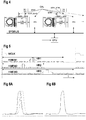
- FIG. 1 shows an example embodiment of a time-to-digital converter system according to the improved calibration concept.
- the TDC system comprises a time-to-digital converter with a ring oscillator RO, a counter CT, an evaluation block EVAL with an intermediate storage STOR, and a histogram block HIST connected to the block containing the counter, the evaluation block and the storage.
- the ring oscillator RO is formed as a fifteen-stage ring oscillator implemented with inverters, each of the inverter outputs connected directly or indirectly with the counter CT, the evaluation block EVAL and the storage element STOR.
- the ring oscillator RO acts as a fine counter and has one output dedicated to counting clock edges of the ring oscillator by the counter CT, which acts as a coarse counter.
- the number of fifteen elements within the ring oscillator RO is chosen arbitrarily for this example and can be readily varied depending on the desired application. For example a switching time of the inverters and the length of the inverter chain determines an oscillator frequency of the ring oscillator RO. In particular, the oscillator frequency may be subject to various process variations such that even ring oscillators manufactured according to the same design may not have the same oscillation frequency within a given precision.
- the evaluation block EVAL is configured to take a start and a stop signal as a basis for determined a time difference between these signals. For example, an actual state of the ring oscillator RO and the counter CT may be stored in the storage element STOR triggered by the start and stop signals. During a measurement operation, the determined time differences resulting from multiple measurements are stored in the histogram block in respective histogram bins as entries associated with the time difference determined in each case.
- the start signal may be provided directly or indirectly as a measurement clock signal MCLK that furthermore triggers some kind of radiation-emitting device, in this example e.g. a VCSEL diode for emitting a laser light pulse.
- the measurement clock MCLK defines a measurement interval TM.
- a stop signal may be provided by a single photon avalanche diode, SPAD, array recording reflections from the radiated pulse.
- the time difference between the start and stop signal indicates the time between emission of a pulse and reception of a reflected pulse, thereby providing a measure for a time-of-flight and distance of the object reflecting the radiation.
- the histogram block has 64 histogram bins. This number should be understood as nonlimiting and could be chosen to be either higher or lower.
- the histogram HMEM shows the result of multiple measurements and the respective distribution in the histogram block HIST.
- the 64 histogram bins are shown in relation to the measurement clock MCLK, respectively the measurement interval TM, within a histogram range HR and a non-covered area, respectively timeframe NC, of the measurement interval TM.
- the information about the length of the histogram range HR and therefore the time width of each bin of the histogram block is not known per se but is the result of a calibration process described in the following.
- the time-to-digital converter system further comprises a calibration block CAL that provides distinct signals STRT as a start signal and STP1 and/or STP2 as stop signals to the time-to-digital converter for effecting a specific time measure resulting from a time difference between the start and stop signals.
- the start signal STRT may be implemented as a measurement clock signal MCLK or being derived from a calibration clock signal CCLK that has a higher frequency than the measurement clock signal MCLK, in this particular example by a predefined ratio of 4. Accordingly, the calibration clock signal CCLK has four clock edges ph0, ph1, ph2, ph3 in each measurement interval defined by the measurement clock MCLK.
- the ratio of the calibration clock signal to the measurement clock signal MCLK and/or its frequency value are known.
- the clock edge ph0 of the calibration clock signal CLK is used as or is coincident with the start signal STRT.
- a first subsequent clock edge ph1 is used as a first stop signal STP1.
- the evaluation block EVAL determines a calibration time difference based on the respective clock edges ph0, ph1 of the calibration clock signals CCLK that can be written to the histogram block HIST, respectively the histogram memory HMEM at a specific position RBIN1 associated with the determined calibration time difference.
- the calibration block CAL is configured to determine a time measure associated with a counter step of the counter based on the predefined ratio between the calibration clock signal CCLK and the measurement clock signal MCLK and the calibration time difference. This may be done directly or by determining the bin number of the histogram block based on the calibration time difference and determining the time measure based on the predefined ratio and the determined bin number RBIN1.
- the time measure can be determined based on the resulting bin number RBIN1 alone, respectively by only evaluating the time difference between the clock edges ph1, ph0.
- a further calibration time difference can be determined based on the time difference between the second stop signal STP2 that is coincident with the clock edge ph2 and the starting clock edge ph0.
- this results in a further bin number RBIN2 in the histogram memory HMEM.
- the time measure associated with the counter step of the counter CT may therefore be determined by employing the difference between the bin number RBIN2 and bin number RBIN1, as also a time difference between the associated clock edges ph1, ph2 is known.
- the clock edges used for the calibration measurement are immediately subsequent to each other in each case.
- single clock edges may be left out, given that all of the used clock edges fall within the same measurement interval TM.
- the predefined ratio between the calibration clock signal CCLK and the measurement clock signal MCLK is chosen as 4, which is both an integer number and a power of 2. Such ratio may be beneficial for practical implementations, but nevertheless other ratios are still possible.
- the calibration clock signal has a higher frequency than the measurement clock signal MCLK such that at least two clock edges of the calibration clock signal fall within the measurement interval TM.
- two stop signals are to be used, like in the example of Figure 3 with RBIN1, RBIN2, it may sufficient if the calibration clock signal CCLK is at least twice the frequency of the measurement clock signal MCLK.
- each histogram bin corresponds to the time width of each counter step as defined by the oscillator, in particular the ring oscillator RO.
- the time measure determined with the calibration measurement indicates the time for a least significant bit, LSB, which is necessary to convert a histogram result into units of time, e.g. picoseconds, and further on into units of length, e.g. millimeter.
- the calibration measurement according to the improved calibration concept can be used for calibrating a TDC system with a single oscillator.
- the improved calibration concept also allows calibrating TDC systems with more than one time-to-digital converter, i.e. more than one oscillator.
- there are various applications for systems with more than one time-to-digital converter e.g. for increasing sensitivity of the TDC system by employing the possibility to receive, respectively record, more reflections, or to use several time-to-digital converters independently, e.g. in a multi-pixel configuration.
- the histograms would not be merged, but it is nevertheless needed to align the time bases of the pixels.
- Figure 4 shows an example of a TDC system with at least two time-to-digital converters, whereas only two of the time-to-digital converters are depicted for better representation.
- the time-to-digital converter system of Figure 4 is based on the embodiment shown in Figure 1 , whereas the structure of the time-to-digital converter is provided a second time and may be provided several times more as indicated by the ellipsis.
- each of the elements of the time-to-digital converters is denoted with reference signs bearing a 1 or 2 behind the reference signs used in Figure 1 and fulfil the same functionality.
- each of the time-to-digital converters performs independent measurements based on respective start and stop signals, the results of the measurements accumulated in the histogram blocks HIST1, HIST2, respectively.
- the calibration block CAL is configured to provide respective start and stop signals STRT, STP1, STP2 for calibration purposes as described above to the respective inputs of the time-to-digital converters. Accordingly, a time measure associated with the counter step of the respective counter of the time-to-digital converter is determined in each case.
- the time measure for each time-to-digital converter can be determined according to one of the approaches described above, i.e. with one or with two stop signals respectively histogram entries.
- the content of three histogram memories HMEM1, HMEM2, HMEM3 correlated to a measurement clock signal MCLK is shown as an example of a TDC system with three time-to-digital converters.
- the three TDCs distinguish at least by their respective histogram ranges HR1, HR2, HR3.
- the peak results in the histogram HMEM1, HMEM2, HMEM3 are not coincident with each other, although they are collected in response to the same events respectively under the same conditions.
- the determined time measures for each of the time-to-digital converters is provided to the CPU by the calibration block CAL, thereby allowing the alignment of recorded entries in the histogram blocks based on the determined time measures for each TDC.
- an overlay of the histogram entries results for example in a coincident distribution as shown in the histogram of Figure 6B .
- the results stored in the single histogram blocks may be merged into a common histogram or histogram-like data structure for having more results, i.e. bin entries, thus increasing the sensitivity of the overall system.
- the results stored in the single histogram blocks are aligned during reading out the entries in the single histogram blocks.
- the histogram entries are denoted with integer bin numbers
- the aligned results may be referenced to non-integer addresses, depending on the value of the time measures respectively calibration factors.
- the calibration i.e. the determination of the time measure associated with the counter steps of the one or more time-to-digital converters can be performed at different times.
- the calibration could be performed before actually performing a measurement, in particular immediately before the actual measurement to have a recordation of the situation at the beginning of the measurement.
- the calibration could be performed after an actual measurement, which has a similar effect.
- even a combination of calibration measurements before and after an actual measurement can be implemented, using e.g. mean values of the determined time measures before and after the measurement.
- the calibration could also be performed in measurement pauses in between different measurement cycles.
- the calibration measurement is performed before an actual measurement, it is also possible to directly process the outputs of the evaluation block of each TDC and adjust the determined time differences of actual measurements based on the determined time measure before storing them into a histogram.
- the adjusted value of each actual measurement could be directly written to a separate memory. This also allows to write non-integer values that could arise from the adjustment.
- the calibration clock signal may be a high speed clock that is globally distributed and carefully balanced. By running the TDCs on two adjacent edges of the clocks, the relative speed of the local ring oscillator can be deduced. Nevertheless, the accuracy of the overall system may be limited by the accuracy of such a high speed clock.
- an external high precision clock could be measured, for example a pulse-per-second, PPS, signal that may be provided by a GPS receiver. The measurement of the external high precision clock is then made using the internal high speed clock, i.e. the calibration clock signal.
Landscapes
- Physics & Mathematics (AREA)
- General Physics & Mathematics (AREA)
- Measurement Of Unknown Time Intervals (AREA)
Abstract
Description
- The present disclosure relates to calibration of a time-to-digital converter system, in particular time-to-digital converter systems employing oscillators.
- A time-to-digital converter (TDC) is a device used to measure a time interval and convert it into digital output. It allows measurements of very short times at high resolution.
- A TDC may be used in time-of-flight cameras, for example, to measure the time an emitted light signal like a laser pulse needs to travel to a reflecting object and back to the camera.
- A well-known technique to implement a TDC uses an oscillator, in particular a ring oscillator and a counter that is being driven by this oscillator, e.g. by a clock edge progressing through the ring oscillator. Such TDC may convert a time difference between respective START and STOP pulses into integer values. These values are then used as addresses for bins in a histogram memory. A downside of this design is that a physical representation of the bin address, e.g. a time difference or a spatial distance, depends on the speed or frequency of the oscillator, which may not be known in advance or may be even varying under different conditions.
- In conventional approaches, the relationship between bin address and physical representation is determined by measuring reference distances.
- An object to be achieved is to provide an improved calibration concept for time-to-digital conversion that provides a higher accuracy.
- This object is achieved with the subject-matter of the independent claims. Embodiments and developments derive from the dependent claims.
- For example, a time-to-digital converter system includes one or more oscillators, in particular ring oscillators, a counter associated with and being driven by each oscillator, an evaluation block connected to each counter and configured for determining a time difference associated with a start signal and a stop signal, and a histogram block with a number of bins for recording entries associated with the time difference. Such a time-to-digital converter system is operated with a measurement clock signal defining a measurement interval. For example, the measurement clock signal drives a radiation-emitting device like a VCSEL diode such that a response or reflection of the emitted radiation, e.g. a light pulse, can be recorded. The measurement interval is usually chosen to match a measurement range of the one or more TDCs.
- The improved calibration concept is based on the idea that a calibration clock signal is provided to the TDC system that has a frequency higher than the measurement clock signal, in particular by a predefined ratio that is known.
- Due to the higher frequency of the calibration clock signal, at least two clock edges of the calibration clock signal fall within the measurement interval defined by the measurement clock signal and hence within the measurement range of the TDC. These at least two clock edges of the calibration clock signal can be used to drive the evaluation block with respective start and stop signals, thereby generating a counter difference, respectively histogram bin address associated with the well-defined clock edges of the calibration clock signal. As a consequence, a time measure associated with a counter step of the counter can be determined, thus having a calibration value for the histogram entries.
- If the frequency or ratio of the calibration clock signal is chosen such that at least three clock edges fall within one measurement interval, it is also possible to perform two different measurements on respective clock edge pairs of the calibration clock signal and to evaluate the results thereof in a differential manner, thereby eliminating e.g. offset effects associated with the measurement.
- In an embodiment of a method for calibrating a time-to-digital converter system as outlined before, the time-to-digital converter system is operated or prepared to be operated with a measurement clock signal defining a measurement interval. According to the improved calibration concept, a calibration clock signal is provided having a frequency higher than the measurement clock signal by a predefined ratio. A selected clock edge of the calibration clock signal is used as a start signal for the evaluation block, and a subsequent clock edge of the calibration clock signal is used as a stop signal for the evaluation block. The evaluation block determines a calibration time difference based on the respective clock edges of the calibration clock signal used as the start signal and the stop signal. A time measure associated with a counter step of the counter is determined based on the predefined ratio and the calibration time difference.
- Depending on the frequency, respectively ratio of the calibration clock signal, the subsequent clock edge used as the stop signal may be a clock edge being immediately subsequent to the clock edge used as the start signal. However, if the frequency or ratio is high enough, some intermediate clock edges may be, so to say, left out under the condition that a time difference between the start signal and the stop signal is shorter than the measurement interval.
- In various implementations of the method, a bin number of the histogram block may be determined based on the calibration time difference, and the time measure is determined based on the predefined ratio and the determined bin number. Hence, for example a more direct relationship between the bin entries in the histogram block and an actual time measure associated with the histogram bins may be established.
- In some implementations where the predefined ratio is at least two, a further subsequent clock edge of the calibration clock signal is used as a further stop signal. The further subsequent clock edge is different from the subsequent clock edge. The evaluation block determines a further calibration time difference based on the respective clock edges of the calibration clock signal used as the start signal and the further stop signal. A further bin number of the histogram block is determined based on the further calibration time difference. The time measure associated with the counter step of the counter is determined based on the predefined ratio and on a difference between the determined further bin number and the determined bin number.
- For example, as the ratio is known, also a time difference between the stop signal, which can also be called a first stop signal, and the further stop signal is known. If any systematic errors like offset errors are present in the system, both the bin number associated with the first stop signal and the bin number associated with the further stop signal are affected by such systematic errors. By forming the difference between the two bin numbers, such systematic errors at least partially cancel out each other.
- While the improved calibration concept will work with any predefined ratio being greater than one, it may be expedient to use predefined ratios of at least two, at least three or at least four. For ease of operation it may also be expedient to choose an integer value for the predefined ratio. This allows, for example, deriving the calibration clock signal and the measurement clock signal from each other, for example by frequency multipliers or dividers, which is more convenient in each case. To this end the predefined ratio may be chosen as an integer value being a power of two.
- Whereas in the previous explanations the improved calibration concept was described in conjunction with a single time-to-digital converter, the improved calibration concept can be easily extended to systems with more than one time-to-digital converter. This will be explained in more detail in the following, taking a second time-to-digital converter as an example. However, it will be apparent to the skilled person that a greater number of time-to-digital converters, e.g. three, four or even more, can be deduced in an analog fashion.
- Hence, in several implementations, the TDC system includes a second time-to-digital converter comprising a second oscillator, in particular a ring oscillator, that is independent of the oscillator of the at least one time-to-digital converter, a second counter being driven by the second oscillator, a second evaluation block connected to the second counter and configured for determining a second time difference associated with a second start signal and a second stop signal, and a signal histogram block with a number of bins for recording entries associated with the second time difference. In such a configuration, the selected clock edge or a further clock edge of the calibration clock signal may be used as the second start signal and a corresponding subsequent clock edge of the calibration clock signal is used as the second stop signal. The definitions of the term "subsequent" as explained above also apply here. The second evaluation block determines a second calibration time difference based on the respective clock edges of the calibration clock signal used as the second start signal and the second stop signal. A second time measure is determined associated with a second counter step of the second counter based on the predefined ratio and the second calibration time difference.
- Accordingly, independent time measures are determined for the first time-to-digital converter and the second time-to-digital converter, allowing alignment of the results of measurements performed with the time-to-digital converters.
- For example, similar to the implementation described for the first time-to-digital converter, a second bin number of the second histogram block can be determined based on the second calibration time difference, and the second time measure can be determined based on the predefined ratio and the determined second bin number. The time measures may be used as a basis for determining calibration factors, e.g. related to a common time base.
- In some of such implementations, recorded entries in the histogram block are aligned with recorded entries in the second histogram block based on the determined time measure and the determined second time measure. Such alignment may be performed during reading out the entries in the first and the second histogram block. For example, while the histogram entries are denoted with integer bin numbers, the aligned results may be referenced to non-integer addresses, depending on the value of the time measures respectively calibration factors.
- It should be apparent to the skilled reader that also for the second time-to-digital converter, the calibration measurement can be performed by employing a further subsequent clock edge of the calibration signal as a further stop signal in order to determine a difference between different bin numbers in the second histogram block, as explained in detail before for the first time-to-digital converter. This also applies to further time-to-digital converters that can be implemented with the TDC system.
- In the various implementations described above, the time measure may be a time span determined based further on a frequency value of the calibration clock signal, i.e. not only on the predefined ratio.
- The frequency value of the calibration clock signal may be determined based on a high precision clock signal, in particular a pulse-per-second, PPS, signal, which may be provided by a GPS receiver or is provided or derived from a crystal oscillator.
- In all of the implementations the calibration result of the improved calibration concept, i.e. the time measure, can be used to convert a histogram result into units of time and further on into units of length, if appropriate. To this end, the calibration measurement may be performed in conjunction with or in relation to an actual measurement with the TDC system in order to have actual measurement results in the histogram block and to have the time measure, i.e. calibration result, when reading out the measurement results from the histogram block.
- In all of the implementations described above, the determination of the calibration time difference and the determination of the time measure based thereon may be performed repeatedly, and a mean time measure may be determined from this repeated determination. Such repeated determination increases the accuracy and the reliability of the measurement result. Hence, evaluation of measurement entries in the histogram block or histogram blocks may be performed based on the mean time measure.
- The improved calibration concept may also be employed in a TDC system as described above which additionally includes a calibration block that is configured for carrying out the method according to one of the implementations described above.
- For example, the calibration block is configured for providing a selected clock edge of a calibration clock signal which has the frequency higher than the measurement clock signal by a predefined ratio to the evaluation block as the start signal and subsequent clock edge of the calibration clock signal as a stop signal. The calibration block is further configured for receiving from the evaluation block a calibration time difference based on the respective clock edges of the calibration clock signal used as the start signal and the stop signal and for determining a time measure associated with a counter step of the counter based on the predefined ratio and the calibration time difference.
- In some implementations the calibration block is further configured for employing a further subsequent clock edge for a second measurement, as described above in detail for the method according to the improved calibration concept.
- Similarly, the calibration block may also be configured for use with two or more time-to-digital converters with respective oscillators, counters etc. as described above, in order to independently determine a second or further time measure associated with a counter step of the counter of the one or more time-to-digital converters. In such configurations, the calibration block may be further configured for aligning recorded entries in the two or more histogram blocks based on the determined time measures.
- Further implementations of the time-to-digital converter system become apparent to the skilled person from the descriptions of the various implementations of the calibration method above.
- The improved timing concept will be explained in more detail in the following with the aid of the drawings. Elements having the same or similar function bear the same reference numerals throughout the drawings. Hence their description is not necessarily repeated in following drawings.
- In the drawings:
- Figure 1
- shows an example embodiment of a time-to-digital converter system according to the improved calibration concept;
- Figure 2
- shows an example time flow diagram for a measurement with a time-to-digital converter system;
- Figure 3
- shows an example time flow diagram for a calibration with a time-to-digital converter system according to the improved calibration concept;
- Figure 4
- shows a further example embodiment of a time-to-digital converter system according to the improved calibration concept;
- Figure 5
- shows a further example time flow diagram for a calibration with a time-to-digital converter system according to the improved calibration concept; and
- Figure 6A and Figure 6B
- show example histograms in connection with the improved calibration concept;
-
Figure 1 shows an example embodiment of a time-to-digital converter system according to the improved calibration concept. The TDC system comprises a time-to-digital converter with a ring oscillator RO, a counter CT, an evaluation block EVAL with an intermediate storage STOR, and a histogram block HIST connected to the block containing the counter, the evaluation block and the storage. - In this example embodiment, the ring oscillator RO is formed as a fifteen-stage ring oscillator implemented with inverters, each of the inverter outputs connected directly or indirectly with the counter CT, the evaluation block EVAL and the storage element STOR. The ring oscillator RO acts as a fine counter and has one output dedicated to counting clock edges of the ring oscillator by the counter CT, which acts as a coarse counter.
- The number of fifteen elements within the ring oscillator RO is chosen arbitrarily for this example and can be readily varied depending on the desired application. For example a switching time of the inverters and the length of the inverter chain determines an oscillator frequency of the ring oscillator RO. In particular, the oscillator frequency may be subject to various process variations such that even ring oscillators manufactured according to the same design may not have the same oscillation frequency within a given precision. The evaluation block EVAL is configured to take a start and a stop signal as a basis for determined a time difference between these signals. For example, an actual state of the ring oscillator RO and the counter CT may be stored in the storage element STOR triggered by the start and stop signals. During a measurement operation, the determined time differences resulting from multiple measurements are stored in the histogram block in respective histogram bins as entries associated with the time difference determined in each case.
- Referring to
Figure 2 , the start signal may be provided directly or indirectly as a measurement clock signal MCLK that furthermore triggers some kind of radiation-emitting device, in this example e.g. a VCSEL diode for emitting a laser light pulse. Hence the measurement clock MCLK defines a measurement interval TM. With reference toFigure 1 , a stop signal may be provided by a single photon avalanche diode, SPAD, array recording reflections from the radiated pulse. Hence, the time difference between the start and stop signal indicates the time between emission of a pulse and reception of a reflected pulse, thereby providing a measure for a time-of-flight and distance of the object reflecting the radiation. - In the example of
Figure 2 , the histogram block has 64 histogram bins. This number should be understood as nonlimiting and could be chosen to be either higher or lower. The histogram HMEM shows the result of multiple measurements and the respective distribution in the histogram block HIST. In the diagram ofFigure 2 , the 64 histogram bins are shown in relation to the measurement clock MCLK, respectively the measurement interval TM, within a histogram range HR and a non-covered area, respectively timeframe NC, of the measurement interval TM. However, the information about the length of the histogram range HR and therefore the time width of each bin of the histogram block is not known per se but is the result of a calibration process described in the following. - Referring back to
Figure 1 , the time-to-digital converter system further comprises a calibration block CAL that provides distinct signals STRT as a start signal and STP1 and/or STP2 as stop signals to the time-to-digital converter for effecting a specific time measure resulting from a time difference between the start and stop signals. - Referring now to
Figure 3 , a signal time diagram of a calibration measurement is shown. The start signal STRT may be implemented as a measurement clock signal MCLK or being derived from a calibration clock signal CCLK that has a higher frequency than the measurement clock signal MCLK, in this particular example by a predefined ratio of 4. Accordingly, the calibration clock signal CCLK has four clock edges ph0, ph1, ph2, ph3 in each measurement interval defined by the measurement clock MCLK. The ratio of the calibration clock signal to the measurement clock signal MCLK and/or its frequency value are known. - As mentioned before, the clock edge ph0 of the calibration clock signal CLK is used as or is coincident with the start signal STRT. A first subsequent clock edge ph1 is used as a first stop signal STP1. Employing the functionality of the evaluation block of the time-to-digital converter, the evaluation block EVAL determines a calibration time difference based on the respective clock edges ph0, ph1 of the calibration clock signals CCLK that can be written to the histogram block HIST, respectively the histogram memory HMEM at a specific position RBIN1 associated with the determined calibration time difference. The calibration block CAL is configured to determine a time measure associated with a counter step of the counter based on the predefined ratio between the calibration clock signal CCLK and the measurement clock signal MCLK and the calibration time difference. This may be done directly or by determining the bin number of the histogram block based on the calibration time difference and determining the time measure based on the predefined ratio and the determined bin number RBIN1.
- Taking as an example a frequency of the calibration clock signal CCLK to be 160 MHz, resulting at a time between two subsequent clock edges ph1, ph0 of 6.25 ns, and a value of the bin number RBIN1 to be 62, the time measure associated with a single bin would result to:

- It should be noted that the time measure can be determined based on the resulting bin number RBIN1 alone, respectively by only evaluating the time difference between the clock edges ph1, ph0. However, in the same manner also a further calibration time difference can be determined based on the time difference between the second stop signal STP2 that is coincident with the clock edge ph2 and the starting clock edge ph0. As can be seen from
Figure 3 , this results in a further bin number RBIN2 in the histogram memory HMEM. The time measure associated with the counter step of the counter CT may therefore be determined by employing the difference between the bin number RBIN2 and bin number RBIN1, as also a time difference between the associated clock edges ph1, ph2 is known. - If, to continue the above example, the further bin number RBIN2 is determined with the value 120, the difference between bin numbers RBIN2 and RBIN 1 results to 120 - 62 = 58, hence the time measure associated with a single bin would result to:

- For example, the clock edges used for the calibration measurement are immediately subsequent to each other in each case. However, depending on the frequency of the calibration clock signal CCLK and/or the predefined ratio to the measurement clock signal MCLK, single clock edges may be left out, given that all of the used clock edges fall within the same measurement interval TM.
- In the example of
Figure 3 , the predefined ratio between the calibration clock signal CCLK and the measurement clock signal MCLK is chosen as 4, which is both an integer number and a power of 2. Such ratio may be beneficial for practical implementations, but nevertheless other ratios are still possible. In particular, if only a time difference between a start pulse and a single stop pulse is evaluated, it may be sufficient that the calibration clock signal has a higher frequency than the measurement clock signal MCLK such that at least two clock edges of the calibration clock signal fall within the measurement interval TM. If two stop signals are to be used, like in the example ofFigure 3 with RBIN1, RBIN2, it may sufficient if the calibration clock signal CCLK is at least twice the frequency of the measurement clock signal MCLK. - It should be apparent to the skilled reader that the time width of each histogram bin corresponds to the time width of each counter step as defined by the oscillator, in particular the ring oscillator RO. Hence, the time measure determined with the calibration measurement indicates the time for a least significant bit, LSB, which is necessary to convert a histogram result into units of time, e.g. picoseconds, and further on into units of length, e.g. millimeter.
- The calibration measurement according to the improved calibration concept can be used for calibrating a TDC system with a single oscillator. However, the improved calibration concept also allows calibrating TDC systems with more than one time-to-digital converter, i.e. more than one oscillator. In particular there are various applications for systems with more than one time-to-digital converter, e.g. for increasing sensitivity of the TDC system by employing the possibility to receive, respectively record, more reflections, or to use several time-to-digital converters independently, e.g. in a multi-pixel configuration.
- For multi-pixel implementations with an imaging lens that are effectively low-pixel count 3D-cameras, the histograms would not be merged, but it is nevertheless needed to align the time bases of the pixels.
-
Figure 4 shows an example of a TDC system with at least two time-to-digital converters, whereas only two of the time-to-digital converters are depicted for better representation. - In particular, the time-to-digital converter system of
Figure 4 is based on the embodiment shown inFigure 1 , whereas the structure of the time-to-digital converter is provided a second time and may be provided several times more as indicated by the ellipsis. In the drawing ofFigure 4 , each of the elements of the time-to-digital converters is denoted with reference signs bearing a 1 or 2 behind the reference signs used inFigure 1 and fulfil the same functionality. In particular, each of the time-to-digital converters performs independent measurements based on respective start and stop signals, the results of the measurements accumulated in the histogram blocks HIST1, HIST2, respectively. - In a similar fashion, the calibration block CAL is configured to provide respective start and stop signals STRT, STP1, STP2 for calibration purposes as described above to the respective inputs of the time-to-digital converters. Accordingly, a time measure associated with the counter step of the respective counter of the time-to-digital converter is determined in each case. In particular, the time measure for each time-to-digital converter can be determined according to one of the approaches described above, i.e. with one or with two stop signals respectively histogram entries.
- Referring to
Figure 5 , the content of three histogram memories HMEM1, HMEM2, HMEM3 correlated to a measurement clock signal MCLK is shown as an example of a TDC system with three time-to-digital converters. As can be seen fromFigure 5 , the three TDCs distinguish at least by their respective histogram ranges HR1, HR2, HR3. Hence, the peak results in the histogram HMEM1, HMEM2, HMEM3 are not coincident with each other, although they are collected in response to the same events respectively under the same conditions. Hence, if the histograms were read out from a CPU over a common system bus SYSBUS as shown inFigure 4 without the calibration respectively the determined time measures, an overlay of the read-out results would look as shown inFigure 6A and would therefore introduce inaccurate results. - However, according to the improved calibration concept, the determined time measures for each of the time-to-digital converters is provided to the CPU by the calibration block CAL, thereby allowing the alignment of recorded entries in the histogram blocks based on the determined time measures for each TDC. Hence, an overlay of the histogram entries results for example in a coincident distribution as shown in the histogram of
Figure 6B . - Hence, in systems, where e.g. multiple SPAD arrays are connected to respective time-to-digital converters, the results stored in the single histogram blocks may be merged into a common histogram or histogram-like data structure for having more results, i.e. bin entries, thus increasing the sensitivity of the overall system. For the merging process, the results stored in the single histogram blocks are aligned during reading out the entries in the single histogram blocks. In this process, while the histogram entries are denoted with integer bin numbers, the aligned results may be referenced to non-integer addresses, depending on the value of the time measures respectively calibration factors.
- In the various embodiments described above, the calibration, i.e. the determination of the time measure associated with the counter steps of the one or more time-to-digital converters can be performed at different times. For example, the calibration could be performed before actually performing a measurement, in particular immediately before the actual measurement to have a recordation of the situation at the beginning of the measurement. Similarly, the calibration could be performed after an actual measurement, which has a similar effect. Moreover, even a combination of calibration measurements before and after an actual measurement can be implemented, using e.g. mean values of the determined time measures before and after the measurement. The calibration could also be performed in measurement pauses in between different measurement cycles.
- All these options allow that the actual measurement results, as e.g. shown as an example in
Figure 5 , could be processed after the actual measurement and even outside the time-to-digital converter system using just the raw measurement data collected in the histogram blocks and the associated time measures determined through the calibration measurement. - However, if the calibration measurement is performed before an actual measurement, it is also possible to directly process the outputs of the evaluation block of each TDC and adjust the determined time differences of actual measurements based on the determined time measure before storing them into a histogram. In a variation of that option, the adjusted value of each actual measurement could be directly written to a separate memory. This also allows to write non-integer values that could arise from the adjustment.
- The calibration clock signal may be a high speed clock that is globally distributed and carefully balanced. By running the TDCs on two adjacent edges of the clocks, the relative speed of the local ring oscillator can be deduced. Nevertheless, the accuracy of the overall system may be limited by the accuracy of such a high speed clock. Hence, for improving the absolute accuracy considerably, an external high precision clock could be measured, for example a pulse-per-second, PPS, signal that may be provided by a GPS receiver. The measurement of the external high precision clock is then made using the internal high speed clock, i.e. the calibration clock signal.
List of Reference Signs RO, RO1, RO2 ring oscillator CT, CT1, CT counter STOR, STOR1, STOR2 storage element EVAL, EVAL1, EVAL2 evaluation block HIST, HIST1, HIST2 histogram block CAL calibration block STRT start signal STP1, STP2 stop signal MCLK measurement clock CCLK calibration clock TM time interval HR, HR1, HR2, HR3 histogram range HMEM, HMEM1, HMEM2, HMEM3 histogram memory NC non-considered time RBIN1, RBIN2 histogram bin address ph0, ph1, ph2, ph3 clock edges SYBUS system bus CPU central processing unit
Claims (15)
- A method for calibrating a time-to-digital converter system with at least one time-to-digital converter comprising an oscillator (RO, RO1, RO2), in particular a ring oscillator, a counter being driven by the oscillator, an evaluation block connected to the counter and configured for determining a time difference associated with a start signal and a stop signal, and a histogram block (HIST, HIST1, HIST2) with a number of bins for recording entries associated with the time difference, the method comprising:- operating or preparing to operate the time-to-digital converter system with a measurement clock signal (MCLK) defining a measurement interval (TM);- providing a calibration clock signal (CCLK) having a frequency higher than the measurement clock signal (MCLK) by a predefined ratio;- using a selected clock edge (ph0) of the calibration clock signal (CCLK) as the start signal (STRT) and a subsequent clock edge (ph1, ph2) of the calibration clock signal (CCLK) as the stop signal (STP1, STP2);- determining, with the evaluation block, a calibration time difference based on the respective clock edges (ph0, ph1, ph2) of the calibration clock signal used as the start signal (STRT) and the stop signal (STP1, STP2); and- determining a time measure associated with a counter step of the counter based on the predefined ratio and the calibration time difference.
- The method according to claim 1, further comprising:- determining a bin number (RBIN1, RBIN2) of the histogram block based on the calibration time difference; and- determining the time measure based on the predefined ratio and the determined bin number.
- The method according to claim 2, wherein the predefined ratio is at least two, the method further comprising:- using a further subsequent clock edge (ph2) of the calibration clock signal (CCLK) as a further stop signal (STP2);- determining, with the evaluation block, a further calibration time difference based on the respective clock edges of the calibration clock signal (CCLK) used as the start signal (STRT) and the further stop signal (STP2);- determining a further bin number (RBIN2) of the histogram block based on the further calibration time difference; and- determining the time measure based on the predefined ratio and on a difference between the determined further bin number (RBIN2) and the determined bin number (RBIN1).
- The method according to one of claims 1 to 3, wherein the predefined ratio is at least three, in particular at least four.
- The method according to one of claims 1 to 4, wherein the predefined ratio is an integer value.
- The method according to one of claims 1 to 5, wherein the time-to-digital converter system includes a second time-to-digital converter comprising a second oscillator (RO2), in particular a ring oscillator, that is independent of the oscillator (RO1) of the at least one time-to-digital converter, a second counter being driven by the second oscillator, a second evaluation block connected to the second counter and configured for determining a second time difference associated with a second start signal and a second stop signal, and a second histogram block (HIST2) with a number of bins for recording entries associated with the second time difference, the method further comprising:using the selected clock edge or a further selected clock edge of the calibration clock signal as the second start signal and a corresponding subsequent clock edge of the calibration clock signal as the second stop signal;determining, with the second evaluation block, a second calibration time difference based on the respective clock edges of the calibration clock signal used as the second start signal and the second stop signal; anddetermining a second time measure associated with a second counter step of the second counter based on the predefined ratio and the second calibration time difference.
- The method according to claim 6, further comprising determining a second bin number of the second histogram block based on the second calibration time difference; and determining the second time measure based on the predefined ratio and the determined second bin number.
- The method according to claim 6 or 7, further comprising aligning recorded entries in the histogram block with recorded entries in the second histogram block based on the determined time measure and the determined second time measure.
- The method according to one of claims 1 to 8, wherein the time measure is a time span determined based further on a frequency value of the calibration clock signal.
- The method according to claim 9, wherein the frequency value of the calibration clock signal is determined based on a high precision clock signal, in particular a pulse-per-second signal.
- The method according to one of claims 1 to 10, wherein the determination of the calibration time difference and the determination of the time measure based thereon is performed repeatedly, and wherein a mean time measure is determined from this repeated determination.
- A time-to-digital converter system, which is operated with a measurement clock signal (MCLK) defining a measurement interval (TM), the system including at least one time-to-digital converter comprising an oscillator (RO, RO1, RO2), in particular a ring oscillator, a counter being driven by the oscillator, an evaluation block connected to the counter and configured for determining a time difference associated with a start signal and a stop signal, a histogram block (HIST, HIST1, HIST2) with a number of bins for recording entries associated with the time difference, and a calibration block (CAL) configured for:providing a selected clock edge (ph0) of a calibration clock signal (CCLK), which has a frequency higher than the measurement clock signal (MCLK) by a predefined ratio, to the evaluation block as the start signal (STRT) and a subsequent clock edge (ph1, ph2) of the calibration clock signal (CCLK) as the stop signal (STP1, STP2);receiving from the evaluation block a calibration time difference based on the respective clock edges of the calibration clock signal used as the start signal (STRT) and the stop signal (STP1, STP2); anddetermining a time measure associated with a counter step of the counter based on the predefined ratio and the calibration time difference.
- The system according to claim 12, wherein the predefined ratio is at least two and the calibration block is further configured for:determining a bin number (RBIN1) of the histogram block based on the calibration time difference;providing a further subsequent clock edge (ph2) of the calibration clock signal (CCLK) to the evaluation block as a further stop signal (STP2);receiving from the evaluation block a further calibration time difference based on the respective clock edges of the calibration clock signal used as the start signal (STRT) and the further stop signal (STP2);determining a further bin number (RBIN2) of the histogram block based on the further calibration time difference; anddetermining the time measure based on the predefined ratio and on a difference between the determined further bin number (RBIN2) and the determined bin number (RBIN1).
- The system according to claim 12 or 13, further including a second time-to-digital converter comprising a second oscillator (RO2), in particular a ring oscillator, that is independent of the oscillator (RO1) of the at least one time-to-digital converter, a second counter being driven by the second oscillator, a second evaluation block connected to the second counter and configured for determining a second time difference associated with a second start signal and a second stop signal, and a second histogram block (HIST2) with a number of bins for recording entries associated with the second time difference, wherein the calibration block is further configured for:providing the selected clock edge or a further selected clock edge of the calibration clock signal to the evaluation block as the second start signal and a corresponding subsequent clock edge of the calibration clock signal as the second stop signal;receiving from the evaluation block a second calibration time difference based on the respective clock edges of the calibration clock signal used as the second start signal and the second stop signal; anddetermining a second time measure associated with a second counter step of the second counter based on the predefined ratio and the second calibration time difference.
- The system according to claim 14, wherein the calibration block is further configured for aligning recorded entries in the histogram block with recorded entries in the second histogram block based on the determined time measure and the determined second time measure.
Priority Applications (4)
| Application Number | Priority Date | Filing Date | Title |
|---|---|---|---|
| CN201780084662.3A CN110235065B (en) | 2017-01-25 | 2017-12-08 | Method for calibrating time-to-digital converter system and time-to-digital converter system |
| US16/477,265 US10732576B2 (en) | 2017-01-25 | 2017-12-08 | Method for calibrating a time-to-digital converter system and time-to-digital converter system |
| PCT/EP2017/082081 WO2018137830A1 (en) | 2017-01-25 | 2017-12-08 | Method for calibrating a time-to-digital converter system and time-to-digital converter system |
| TW107101831A TWI660590B (en) | 2017-01-25 | 2018-01-18 | Method for calibrating a time-to-digital converter system and time-to-digital converter system |
Applications Claiming Priority (1)
| Application Number | Priority Date | Filing Date | Title |
|---|---|---|---|
| US201762450442P | 2017-01-25 | 2017-01-25 |
Publications (2)
| Publication Number | Publication Date |
|---|---|
| EP3355133A1 true EP3355133A1 (en) | 2018-08-01 |
| EP3355133B1 EP3355133B1 (en) | 2019-10-30 |
Family
ID=58018004
Family Applications (1)
| Application Number | Title | Priority Date | Filing Date |
|---|---|---|---|
| EP17155828.1A Active EP3355133B1 (en) | 2017-01-25 | 2017-02-13 | Method for calibrating a time-to-digital converter system and time-to-digital converter system |
Country Status (5)
| Country | Link |
|---|---|
| US (1) | US10732576B2 (en) |
| EP (1) | EP3355133B1 (en) |
| CN (1) | CN110235065B (en) |
| TW (1) | TWI660590B (en) |
| WO (1) | WO2018137830A1 (en) |
Cited By (2)
| Publication number | Priority date | Publication date | Assignee | Title |
|---|---|---|---|---|
| WO2021115652A1 (en) * | 2019-12-11 | 2021-06-17 | Ibeo Automotive Systems GmbH | Device and method for generating test data for testing a distance determination in an optical time-of-flight measurement |
| US11686826B2 (en) | 2017-09-22 | 2023-06-27 | Ams Ag | Measuring time-of-flight using a plurality of detector subsystems and histogram storage |
Families Citing this family (12)
| Publication number | Priority date | Publication date | Assignee | Title |
|---|---|---|---|---|
| WO2019005260A1 (en) | 2017-06-29 | 2019-01-03 | Apple Inc. | Time-of-flight depth mapping with parallax compensation |
| WO2019125349A1 (en) | 2017-12-18 | 2019-06-27 | Montrose Laboratories Llc | Time-of-flight sensing using an addressable array of emitters |
| EP3521856B1 (en) | 2018-01-31 | 2023-09-13 | ams AG | Time-of-flight arrangement and method for a time-of-flight measurement |
| WO2020167338A1 (en) | 2019-02-11 | 2020-08-20 | Apple Inc. | Depth sensing using a sparse array of pulsed beams |
| US11500094B2 (en) | 2019-06-10 | 2022-11-15 | Apple Inc. | Selection of pulse repetition intervals for sensing time of flight |
| US11555900B1 (en) | 2019-07-17 | 2023-01-17 | Apple Inc. | LiDAR system with enhanced area coverage |
| US11733359B2 (en) * | 2019-12-03 | 2023-08-22 | Apple Inc. | Configurable array of single-photon detectors |
| US12442926B2 (en) | 2021-02-04 | 2025-10-14 | Apple Inc. | Time-of-flight depth sensing with improved linearity |
| US12196860B2 (en) | 2021-03-02 | 2025-01-14 | Apple Inc. | Depth sensor calibration using internal reflections |
| US11681028B2 (en) | 2021-07-18 | 2023-06-20 | Apple Inc. | Close-range measurement of time of flight using parallax shift |
| EP4303669A1 (en) * | 2022-07-07 | 2024-01-10 | Magics Technologies | Improved delay line calibration method |
| CN115857307B (en) * | 2022-11-22 | 2025-07-15 | 思瑞浦微电子科技(苏州)股份有限公司 | Converter calibration method and system |
Citations (2)
| Publication number | Priority date | Publication date | Assignee | Title |
|---|---|---|---|---|
| US20050119846A1 (en) * | 2003-11-28 | 2005-06-02 | Agilent Technologies, Inc. | Calibration method of time measurement apparatus |
| US20120249195A1 (en) * | 2011-04-01 | 2012-10-04 | Xiaochuan Guo | Clock generating apparatus and frequency calibrating method of the clock generating apparatus |
Family Cites Families (13)
| Publication number | Priority date | Publication date | Assignee | Title |
|---|---|---|---|---|
| US6754613B2 (en) * | 2000-03-17 | 2004-06-22 | Vector 12 Corporation | High resolution time-to-digital converter |
| JP3633892B2 (en) | 2001-09-05 | 2005-03-30 | Fdk株式会社 | choke coil |
| TW574510B (en) | 2002-05-31 | 2004-02-01 | Dian-Rung Chen | Fiber interferometer and the interference method thereof |
| EP1852756B1 (en) * | 2005-02-24 | 2010-09-01 | Seiko Epson Corporation | Clock signal outputting device and its control method |
| GB0902822D0 (en) | 2009-02-19 | 2009-04-08 | Cmosis Nv | Analog-to-digital conversation in pixel arrays |
| US8228219B2 (en) * | 2010-06-15 | 2012-07-24 | Infineon Technologies Ag | Time-to-digital converter with calibration |
| TW201324325A (en) | 2011-12-12 | 2013-06-16 | Univ Nan Kai Technology | Digital device for updating device time based on data stored time and method thereof |
| JP6077290B2 (en) * | 2012-12-06 | 2017-02-08 | ルネサスエレクトロニクス株式会社 | Semiconductor device, wireless communication terminal, and semiconductor device control method |
| CN103257569B (en) * | 2013-05-23 | 2015-10-21 | 龙芯中科技术有限公司 | Time measuring circuit, method and system |
| US9331722B2 (en) | 2013-12-26 | 2016-05-03 | Intel IP Corporation | Feedback calibration of digital to time converter |
| TWI534469B (en) | 2014-06-17 | 2016-05-21 | 信泰光學(深圳)有限公司 | Wide-angle projection lens |
| DE102014108762B4 (en) * | 2014-06-23 | 2023-11-16 | Intel Corporation | A circuit, a time-to-digital converter, an integrated circuit, a transmitter, a receiver and a transceiver |
| US9529336B2 (en) | 2015-02-25 | 2016-12-27 | Taiwan Semiconductor Manufacturing Company, Ltd. | Analog to digital converter compatible with image sensor readout |
-
2017
- 2017-02-13 EP EP17155828.1A patent/EP3355133B1/en active Active
- 2017-12-08 CN CN201780084662.3A patent/CN110235065B/en active Active
- 2017-12-08 US US16/477,265 patent/US10732576B2/en active Active
- 2017-12-08 WO PCT/EP2017/082081 patent/WO2018137830A1/en not_active Ceased
-
2018
- 2018-01-18 TW TW107101831A patent/TWI660590B/en active
Patent Citations (2)
| Publication number | Priority date | Publication date | Assignee | Title |
|---|---|---|---|---|
| US20050119846A1 (en) * | 2003-11-28 | 2005-06-02 | Agilent Technologies, Inc. | Calibration method of time measurement apparatus |
| US20120249195A1 (en) * | 2011-04-01 | 2012-10-04 | Xiaochuan Guo | Clock generating apparatus and frequency calibrating method of the clock generating apparatus |
Cited By (3)
| Publication number | Priority date | Publication date | Assignee | Title |
|---|---|---|---|---|
| US11686826B2 (en) | 2017-09-22 | 2023-06-27 | Ams Ag | Measuring time-of-flight using a plurality of detector subsystems and histogram storage |
| WO2021115652A1 (en) * | 2019-12-11 | 2021-06-17 | Ibeo Automotive Systems GmbH | Device and method for generating test data for testing a distance determination in an optical time-of-flight measurement |
| JP2023505364A (en) * | 2019-12-11 | 2023-02-08 | イベオ オートモーティブ システムズ ゲーエムベーハー | Apparatus and method for generating test data for testing distance determination in optical time-of-flight measurements |
Also Published As
| Publication number | Publication date |
|---|---|
| US20190361404A1 (en) | 2019-11-28 |
| US10732576B2 (en) | 2020-08-04 |
| WO2018137830A1 (en) | 2018-08-02 |
| CN110235065B (en) | 2021-04-06 |
| EP3355133B1 (en) | 2019-10-30 |
| CN110235065A (en) | 2019-09-13 |
| TWI660590B (en) | 2019-05-21 |
| TW201832474A (en) | 2018-09-01 |
Similar Documents
| Publication | Publication Date | Title |
|---|---|---|
| EP3355133B1 (en) | Method for calibrating a time-to-digital converter system and time-to-digital converter system | |
| US11639990B2 (en) | Digital pixels and operating methods thereof | |
| CN110596722B (en) | System and method for measuring flight time distance with adjustable histogram | |
| Manuzzato et al. | A $64\times 64$-Pixel Flash LiDAR SPAD Imager with Distributed Pixel-to-Pixel Correlation for Background Rejection, Tunable Automatic Pixel Sensitivity and First-Last Event Detection Strategies for Space Applications | |
| US11619914B2 (en) | Arrayed time to digital converter | |
| CN110596725B (en) | Time-of-flight measurement method and system based on interpolation | |
| CN110221272B (en) | Time flight depth camera and anti-interference distance measurement method | |
| DE10201670B4 (en) | Timing system and an associated distance measuring system | |
| US9720076B2 (en) | Calibration circuitry and method for a time of flight imaging system | |
| US10671025B2 (en) | Time-to-digital converter and conversion method | |
| US20220082698A1 (en) | Depth camera and multi-frequency modulation and demodulation-based noise-reduction distance measurement method | |
| US20210181316A1 (en) | Time-of-flight-based distance measurement system and method | |
| CN110622038B (en) | Optical sensor, electronic device, computing device, and method for measuring distance between optical sensor and detection object | |
| WO2021051480A1 (en) | Dynamic histogram drawing-based time of flight distance measurement method and measurement system | |
| US20220043129A1 (en) | Time flight depth camera and multi-frequency modulation and demodulation distance measuring method | |
| US20230236297A1 (en) | Systems and Methods for High Precision Direct Time-of-Flight Lidar in the Presence of Strong Pile-Up | |
| Sesta et al. | Range-finding SPAD array with smart laser-spot tracking and TDC sharing for background suppression | |
| CN113484870A (en) | Ranging method and apparatus, terminal, and non-volatile computer-readable storage medium | |
| US20220244391A1 (en) | Time-of-flight depth sensing with improved linearity | |
| Villa et al. | CMOS single photon sensor with in-pixel TDC for Time-of-Flight applications | |
| CN114895317B (en) | Distance calculation methods, chips, cameras, and storage media | |
| US20240069199A1 (en) | Ranging device | |
| US12482055B2 (en) | Systems and methods for memory-efficient pixel histogramming | |
| RU2155322C1 (en) | Optical range finder | |
| Markovic et al. | Smart-pixel with SPAD detector and time-to-digital converter for time-correlated single photon counting |
Legal Events
| Date | Code | Title | Description |
|---|---|---|---|
| PUAI | Public reference made under article 153(3) epc to a published international application that has entered the european phase |
Free format text: ORIGINAL CODE: 0009012 |
|
| STAA | Information on the status of an ep patent application or granted ep patent |
Free format text: STATUS: THE APPLICATION HAS BEEN PUBLISHED |
|
| AK | Designated contracting states |
Kind code of ref document: A1 Designated state(s): AL AT BE BG CH CY CZ DE DK EE ES FI FR GB GR HR HU IE IS IT LI LT LU LV MC MK MT NL NO PL PT RO RS SE SI SK SM TR |
|
| AX | Request for extension of the european patent |
Extension state: BA ME |
|
| RAP1 | Party data changed (applicant data changed or rights of an application transferred) |
Owner name: AMS AG |
|
| STAA | Information on the status of an ep patent application or granted ep patent |
Free format text: STATUS: REQUEST FOR EXAMINATION WAS MADE |
|
| 17P | Request for examination filed |
Effective date: 20190118 |
|
| RBV | Designated contracting states (corrected) |
Designated state(s): AL AT BE BG CH CY CZ DE DK EE ES FI FR GB GR HR HU IE IS IT LI LT LU LV MC MK MT NL NO PL PT RO RS SE SI SK SM TR |
|
| GRAP | Despatch of communication of intention to grant a patent |
Free format text: ORIGINAL CODE: EPIDOSNIGR1 |
|
| STAA | Information on the status of an ep patent application or granted ep patent |
Free format text: STATUS: GRANT OF PATENT IS INTENDED |
|
| INTG | Intention to grant announced |
Effective date: 20190717 |
|
| RIN1 | Information on inventor provided before grant (corrected) |
Inventor name: MAUTNER, CHRISTIAN Inventor name: BAHNMUELLER, FRIEDRICH Inventor name: GLOVER, KERRY |
|
| GRAS | Grant fee paid |
Free format text: ORIGINAL CODE: EPIDOSNIGR3 |
|
| GRAA | (expected) grant |
Free format text: ORIGINAL CODE: 0009210 |
|
| STAA | Information on the status of an ep patent application or granted ep patent |
Free format text: STATUS: THE PATENT HAS BEEN GRANTED |
|
| AK | Designated contracting states |
Kind code of ref document: B1 Designated state(s): AL AT BE BG CH CY CZ DE DK EE ES FI FR GB GR HR HU IE IS IT LI LT LU LV MC MK MT NL NO PL PT RO RS SE SI SK SM TR |
|
| REG | Reference to a national code |
Ref country code: GB Ref legal event code: FG4D |
|
| REG | Reference to a national code |
Ref country code: CH Ref legal event code: EP |
|
| REG | Reference to a national code |
Ref country code: AT Ref legal event code: REF Ref document number: 1196812 Country of ref document: AT Kind code of ref document: T Effective date: 20191115 |
|
| REG | Reference to a national code |
Ref country code: DE Ref legal event code: R096 Ref document number: 602017008127 Country of ref document: DE |
|
| REG | Reference to a national code |
Ref country code: IE Ref legal event code: FG4D |
|
| REG | Reference to a national code |
Ref country code: LT Ref legal event code: MG4D |
|
| PG25 | Lapsed in a contracting state [announced via postgrant information from national office to epo] |
Ref country code: PT Free format text: LAPSE BECAUSE OF FAILURE TO SUBMIT A TRANSLATION OF THE DESCRIPTION OR TO PAY THE FEE WITHIN THE PRESCRIBED TIME-LIMIT Effective date: 20200302 Ref country code: SE Free format text: LAPSE BECAUSE OF FAILURE TO SUBMIT A TRANSLATION OF THE DESCRIPTION OR TO PAY THE FEE WITHIN THE PRESCRIBED TIME-LIMIT Effective date: 20191030 Ref country code: LV Free format text: LAPSE BECAUSE OF FAILURE TO SUBMIT A TRANSLATION OF THE DESCRIPTION OR TO PAY THE FEE WITHIN THE PRESCRIBED TIME-LIMIT Effective date: 20191030 Ref country code: FI Free format text: LAPSE BECAUSE OF FAILURE TO SUBMIT A TRANSLATION OF THE DESCRIPTION OR TO PAY THE FEE WITHIN THE PRESCRIBED TIME-LIMIT Effective date: 20191030 Ref country code: NO Free format text: LAPSE BECAUSE OF FAILURE TO SUBMIT A TRANSLATION OF THE DESCRIPTION OR TO PAY THE FEE WITHIN THE PRESCRIBED TIME-LIMIT Effective date: 20200130 Ref country code: BG Free format text: LAPSE BECAUSE OF FAILURE TO SUBMIT A TRANSLATION OF THE DESCRIPTION OR TO PAY THE FEE WITHIN THE PRESCRIBED TIME-LIMIT Effective date: 20200130 Ref country code: PL Free format text: LAPSE BECAUSE OF FAILURE TO SUBMIT A TRANSLATION OF THE DESCRIPTION OR TO PAY THE FEE WITHIN THE PRESCRIBED TIME-LIMIT Effective date: 20191030 Ref country code: GR Free format text: LAPSE BECAUSE OF FAILURE TO SUBMIT A TRANSLATION OF THE DESCRIPTION OR TO PAY THE FEE WITHIN THE PRESCRIBED TIME-LIMIT Effective date: 20200131 Ref country code: LT Free format text: LAPSE BECAUSE OF FAILURE TO SUBMIT A TRANSLATION OF THE DESCRIPTION OR TO PAY THE FEE WITHIN THE PRESCRIBED TIME-LIMIT Effective date: 20191030 Ref country code: NL Free format text: LAPSE BECAUSE OF FAILURE TO SUBMIT A TRANSLATION OF THE DESCRIPTION OR TO PAY THE FEE WITHIN THE PRESCRIBED TIME-LIMIT Effective date: 20191030 |
|
| REG | Reference to a national code |
Ref country code: NL Ref legal event code: MP Effective date: 20191030 |
|
| PG25 | Lapsed in a contracting state [announced via postgrant information from national office to epo] |
Ref country code: HR Free format text: LAPSE BECAUSE OF FAILURE TO SUBMIT A TRANSLATION OF THE DESCRIPTION OR TO PAY THE FEE WITHIN THE PRESCRIBED TIME-LIMIT Effective date: 20191030 Ref country code: RS Free format text: LAPSE BECAUSE OF FAILURE TO SUBMIT A TRANSLATION OF THE DESCRIPTION OR TO PAY THE FEE WITHIN THE PRESCRIBED TIME-LIMIT Effective date: 20191030 Ref country code: IS Free format text: LAPSE BECAUSE OF FAILURE TO SUBMIT A TRANSLATION OF THE DESCRIPTION OR TO PAY THE FEE WITHIN THE PRESCRIBED TIME-LIMIT Effective date: 20200229 |
|
| PG25 | Lapsed in a contracting state [announced via postgrant information from national office to epo] |
Ref country code: AL Free format text: LAPSE BECAUSE OF FAILURE TO SUBMIT A TRANSLATION OF THE DESCRIPTION OR TO PAY THE FEE WITHIN THE PRESCRIBED TIME-LIMIT Effective date: 20191030 |
|
| PG25 | Lapsed in a contracting state [announced via postgrant information from national office to epo] |
Ref country code: EE Free format text: LAPSE BECAUSE OF FAILURE TO SUBMIT A TRANSLATION OF THE DESCRIPTION OR TO PAY THE FEE WITHIN THE PRESCRIBED TIME-LIMIT Effective date: 20191030 Ref country code: CZ Free format text: LAPSE BECAUSE OF FAILURE TO SUBMIT A TRANSLATION OF THE DESCRIPTION OR TO PAY THE FEE WITHIN THE PRESCRIBED TIME-LIMIT Effective date: 20191030 Ref country code: RO Free format text: LAPSE BECAUSE OF FAILURE TO SUBMIT A TRANSLATION OF THE DESCRIPTION OR TO PAY THE FEE WITHIN THE PRESCRIBED TIME-LIMIT Effective date: 20191030 Ref country code: ES Free format text: LAPSE BECAUSE OF FAILURE TO SUBMIT A TRANSLATION OF THE DESCRIPTION OR TO PAY THE FEE WITHIN THE PRESCRIBED TIME-LIMIT Effective date: 20191030 Ref country code: DK Free format text: LAPSE BECAUSE OF FAILURE TO SUBMIT A TRANSLATION OF THE DESCRIPTION OR TO PAY THE FEE WITHIN THE PRESCRIBED TIME-LIMIT Effective date: 20191030 |
|
| REG | Reference to a national code |
Ref country code: DE Ref legal event code: R097 Ref document number: 602017008127 Country of ref document: DE |
|
| REG | Reference to a national code |
Ref country code: AT Ref legal event code: MK05 Ref document number: 1196812 Country of ref document: AT Kind code of ref document: T Effective date: 20191030 |
|
| PG25 | Lapsed in a contracting state [announced via postgrant information from national office to epo] |
Ref country code: SM Free format text: LAPSE BECAUSE OF FAILURE TO SUBMIT A TRANSLATION OF THE DESCRIPTION OR TO PAY THE FEE WITHIN THE PRESCRIBED TIME-LIMIT Effective date: 20191030 Ref country code: IT Free format text: LAPSE BECAUSE OF FAILURE TO SUBMIT A TRANSLATION OF THE DESCRIPTION OR TO PAY THE FEE WITHIN THE PRESCRIBED TIME-LIMIT Effective date: 20191030 Ref country code: SK Free format text: LAPSE BECAUSE OF FAILURE TO SUBMIT A TRANSLATION OF THE DESCRIPTION OR TO PAY THE FEE WITHIN THE PRESCRIBED TIME-LIMIT Effective date: 20191030 |
|
| PLBE | No opposition filed within time limit |
Free format text: ORIGINAL CODE: 0009261 |
|
| STAA | Information on the status of an ep patent application or granted ep patent |
Free format text: STATUS: NO OPPOSITION FILED WITHIN TIME LIMIT |
|
| REG | Reference to a national code |
Ref country code: CH Ref legal event code: PL |
|
| 26N | No opposition filed |
Effective date: 20200731 |
|
| REG | Reference to a national code |
Ref country code: BE Ref legal event code: MM Effective date: 20200229 |
|
| PG25 | Lapsed in a contracting state [announced via postgrant information from national office to epo] |
Ref country code: MC Free format text: LAPSE BECAUSE OF FAILURE TO SUBMIT A TRANSLATION OF THE DESCRIPTION OR TO PAY THE FEE WITHIN THE PRESCRIBED TIME-LIMIT Effective date: 20191030 Ref country code: LU Free format text: LAPSE BECAUSE OF NON-PAYMENT OF DUE FEES Effective date: 20200213 |
|
| REG | Reference to a national code |
Ref country code: DE Ref legal event code: R082 Ref document number: 602017008127 Country of ref document: DE Representative=s name: EPPING HERMANN FISCHER PATENTANWALTSGESELLSCHA, DE Ref country code: DE Ref legal event code: R081 Ref document number: 602017008127 Country of ref document: DE Owner name: SCIOSENSE B.V., NL Free format text: FORMER OWNER: AMS AG, PREMSTAETTEN, AT |
|
| PG25 | Lapsed in a contracting state [announced via postgrant information from national office to epo] |
Ref country code: SI Free format text: LAPSE BECAUSE OF FAILURE TO SUBMIT A TRANSLATION OF THE DESCRIPTION OR TO PAY THE FEE WITHIN THE PRESCRIBED TIME-LIMIT Effective date: 20191030 Ref country code: CH Free format text: LAPSE BECAUSE OF NON-PAYMENT OF DUE FEES Effective date: 20200229 Ref country code: LI Free format text: LAPSE BECAUSE OF NON-PAYMENT OF DUE FEES Effective date: 20200229 Ref country code: AT Free format text: LAPSE BECAUSE OF FAILURE TO SUBMIT A TRANSLATION OF THE DESCRIPTION OR TO PAY THE FEE WITHIN THE PRESCRIBED TIME-LIMIT Effective date: 20191030 |
|
| PG25 | Lapsed in a contracting state [announced via postgrant information from national office to epo] |
Ref country code: IE Free format text: LAPSE BECAUSE OF NON-PAYMENT OF DUE FEES Effective date: 20200213 |
|
| REG | Reference to a national code |
Ref country code: GB Ref legal event code: 732E Free format text: REGISTERED BETWEEN 20210107 AND 20210113 |
|
| PG25 | Lapsed in a contracting state [announced via postgrant information from national office to epo] |
Ref country code: BE Free format text: LAPSE BECAUSE OF NON-PAYMENT OF DUE FEES Effective date: 20200229 |
|
| PG25 | Lapsed in a contracting state [announced via postgrant information from national office to epo] |
Ref country code: TR Free format text: LAPSE BECAUSE OF FAILURE TO SUBMIT A TRANSLATION OF THE DESCRIPTION OR TO PAY THE FEE WITHIN THE PRESCRIBED TIME-LIMIT Effective date: 20191030 Ref country code: MT Free format text: LAPSE BECAUSE OF FAILURE TO SUBMIT A TRANSLATION OF THE DESCRIPTION OR TO PAY THE FEE WITHIN THE PRESCRIBED TIME-LIMIT Effective date: 20191030 Ref country code: CY Free format text: LAPSE BECAUSE OF FAILURE TO SUBMIT A TRANSLATION OF THE DESCRIPTION OR TO PAY THE FEE WITHIN THE PRESCRIBED TIME-LIMIT Effective date: 20191030 |
|
| PG25 | Lapsed in a contracting state [announced via postgrant information from national office to epo] |
Ref country code: MK Free format text: LAPSE BECAUSE OF FAILURE TO SUBMIT A TRANSLATION OF THE DESCRIPTION OR TO PAY THE FEE WITHIN THE PRESCRIBED TIME-LIMIT Effective date: 20191030 |
|
| P01 | Opt-out of the competence of the unified patent court (upc) registered |
Effective date: 20230515 |
|
| PGFP | Annual fee paid to national office [announced via postgrant information from national office to epo] |
Ref country code: GB Payment date: 20260219 Year of fee payment: 10 |
|
| PGFP | Annual fee paid to national office [announced via postgrant information from national office to epo] |
Ref country code: DE Payment date: 20260223 Year of fee payment: 10 |
|
| PGFP | Annual fee paid to national office [announced via postgrant information from national office to epo] |
Ref country code: FR Payment date: 20260223 Year of fee payment: 10 |