EP3352212A1 - Power electronics package and method of manufacturing thereof - Google Patents
Power electronics package and method of manufacturing thereof Download PDFInfo
- Publication number
- EP3352212A1 EP3352212A1 EP17152916.7A EP17152916A EP3352212A1 EP 3352212 A1 EP3352212 A1 EP 3352212A1 EP 17152916 A EP17152916 A EP 17152916A EP 3352212 A1 EP3352212 A1 EP 3352212A1
- Authority
- EP
- European Patent Office
- Prior art keywords
- layer
- glass substrate
- electronics package
- thickness
- substrate
- Prior art date
- Legal status (The legal status is an assumption and is not a legal conclusion. Google has not performed a legal analysis and makes no representation as to the accuracy of the status listed.)
- Granted
Links
Images





Classifications
-
- H—ELECTRICITY
- H10—SEMICONDUCTOR DEVICES; ELECTRIC SOLID-STATE DEVICES NOT OTHERWISE PROVIDED FOR
- H10W—GENERIC PACKAGES, INTERCONNECTIONS, CONNECTORS OR OTHER CONSTRUCTIONAL DETAILS OF DEVICES COVERED BY CLASS H10
- H10W70/00—Package substrates; Interposers; Redistribution layers [RDL]
- H10W70/01—Manufacture or treatment
- H10W70/05—Manufacture or treatment of insulating or insulated package substrates, or of interposers, or of redistribution layers
- H10W70/08—Manufacture or treatment of insulating or insulated package substrates, or of interposers, or of redistribution layers by depositing layers on the chip or wafer, e.g. "chip-first" RDLs
- H10W70/09—Manufacture or treatment of insulating or insulated package substrates, or of interposers, or of redistribution layers by depositing layers on the chip or wafer, e.g. "chip-first" RDLs extending onto an encapsulation that laterally surrounds the chip or wafer, e.g. fan-out wafer level package [FOWLP] RDLs
-
- H—ELECTRICITY
- H10—SEMICONDUCTOR DEVICES; ELECTRIC SOLID-STATE DEVICES NOT OTHERWISE PROVIDED FOR
- H10W—GENERIC PACKAGES, INTERCONNECTIONS, CONNECTORS OR OTHER CONSTRUCTIONAL DETAILS OF DEVICES COVERED BY CLASS H10
- H10W70/00—Package substrates; Interposers; Redistribution layers [RDL]
- H10W70/01—Manufacture or treatment
- H10W70/05—Manufacture or treatment of insulating or insulated package substrates, or of interposers, or of redistribution layers
- H10W70/093—Connecting or disconnecting other interconnections thereto or therefrom, e.g. connecting bond wires or bumps
-
- H—ELECTRICITY
- H10—SEMICONDUCTOR DEVICES; ELECTRIC SOLID-STATE DEVICES NOT OTHERWISE PROVIDED FOR
- H10W—GENERIC PACKAGES, INTERCONNECTIONS, CONNECTORS OR OTHER CONSTRUCTIONAL DETAILS OF DEVICES COVERED BY CLASS H10
- H10W70/00—Package substrates; Interposers; Redistribution layers [RDL]
- H10W70/60—Insulating or insulated package substrates; Interposers; Redistribution layers
- H10W70/611—Insulating or insulated package substrates; Interposers; Redistribution layers for connecting multiple chips together
- H10W70/614—Insulating or insulated package substrates; Interposers; Redistribution layers for connecting multiple chips together the multiple chips being integrally enclosed
-
- H—ELECTRICITY
- H10—SEMICONDUCTOR DEVICES; ELECTRIC SOLID-STATE DEVICES NOT OTHERWISE PROVIDED FOR
- H10W—GENERIC PACKAGES, INTERCONNECTIONS, CONNECTORS OR OTHER CONSTRUCTIONAL DETAILS OF DEVICES COVERED BY CLASS H10
- H10W70/00—Package substrates; Interposers; Redistribution layers [RDL]
- H10W70/60—Insulating or insulated package substrates; Interposers; Redistribution layers
- H10W70/67—Insulating or insulated package substrates; Interposers; Redistribution layers characterised by their insulating layers or insulating parts
- H10W70/68—Shapes or dispositions thereof
-
- H—ELECTRICITY
- H10—SEMICONDUCTOR DEVICES; ELECTRIC SOLID-STATE DEVICES NOT OTHERWISE PROVIDED FOR
- H10W—GENERIC PACKAGES, INTERCONNECTIONS, CONNECTORS OR OTHER CONSTRUCTIONAL DETAILS OF DEVICES COVERED BY CLASS H10
- H10W70/00—Package substrates; Interposers; Redistribution layers [RDL]
- H10W70/60—Insulating or insulated package substrates; Interposers; Redistribution layers
- H10W70/67—Insulating or insulated package substrates; Interposers; Redistribution layers characterised by their insulating layers or insulating parts
- H10W70/69—Insulating materials thereof
- H10W70/692—Ceramics or glasses
-
- H—ELECTRICITY
- H10—SEMICONDUCTOR DEVICES; ELECTRIC SOLID-STATE DEVICES NOT OTHERWISE PROVIDED FOR
- H10W—GENERIC PACKAGES, INTERCONNECTIONS, CONNECTORS OR OTHER CONSTRUCTIONAL DETAILS OF DEVICES COVERED BY CLASS H10
- H10W90/00—Package configurations
-
- H—ELECTRICITY
- H10—SEMICONDUCTOR DEVICES; ELECTRIC SOLID-STATE DEVICES NOT OTHERWISE PROVIDED FOR
- H10W—GENERIC PACKAGES, INTERCONNECTIONS, CONNECTORS OR OTHER CONSTRUCTIONAL DETAILS OF DEVICES COVERED BY CLASS H10
- H10W70/00—Package substrates; Interposers; Redistribution layers [RDL]
- H10W70/60—Insulating or insulated package substrates; Interposers; Redistribution layers
-
- H—ELECTRICITY
- H10—SEMICONDUCTOR DEVICES; ELECTRIC SOLID-STATE DEVICES NOT OTHERWISE PROVIDED FOR
- H10W—GENERIC PACKAGES, INTERCONNECTIONS, CONNECTORS OR OTHER CONSTRUCTIONAL DETAILS OF DEVICES COVERED BY CLASS H10
- H10W70/00—Package substrates; Interposers; Redistribution layers [RDL]
- H10W70/60—Insulating or insulated package substrates; Interposers; Redistribution layers
- H10W70/67—Insulating or insulated package substrates; Interposers; Redistribution layers characterised by their insulating layers or insulating parts
- H10W70/68—Shapes or dispositions thereof
- H10W70/682—Shapes or dispositions thereof comprising holes having chips therein
-
- H—ELECTRICITY
- H10—SEMICONDUCTOR DEVICES; ELECTRIC SOLID-STATE DEVICES NOT OTHERWISE PROVIDED FOR
- H10W—GENERIC PACKAGES, INTERCONNECTIONS, CONNECTORS OR OTHER CONSTRUCTIONAL DETAILS OF DEVICES COVERED BY CLASS H10
- H10W72/00—Interconnections or connectors in packages
- H10W72/071—Connecting or disconnecting
- H10W72/073—Connecting or disconnecting of die-attach connectors
-
- H—ELECTRICITY
- H10—SEMICONDUCTOR DEVICES; ELECTRIC SOLID-STATE DEVICES NOT OTHERWISE PROVIDED FOR
- H10W—GENERIC PACKAGES, INTERCONNECTIONS, CONNECTORS OR OTHER CONSTRUCTIONAL DETAILS OF DEVICES COVERED BY CLASS H10
- H10W72/00—Interconnections or connectors in packages
- H10W72/851—Dispositions of multiple connectors or interconnections
- H10W72/874—On different surfaces
-
- H—ELECTRICITY
- H10—SEMICONDUCTOR DEVICES; ELECTRIC SOLID-STATE DEVICES NOT OTHERWISE PROVIDED FOR
- H10W—GENERIC PACKAGES, INTERCONNECTIONS, CONNECTORS OR OTHER CONSTRUCTIONAL DETAILS OF DEVICES COVERED BY CLASS H10
- H10W72/00—Interconnections or connectors in packages
- H10W72/90—Bond pads, in general
- H10W72/921—Structures or relative sizes of bond pads
- H10W72/926—Multiple bond pads having different sizes
-
- H—ELECTRICITY
- H10—SEMICONDUCTOR DEVICES; ELECTRIC SOLID-STATE DEVICES NOT OTHERWISE PROVIDED FOR
- H10W—GENERIC PACKAGES, INTERCONNECTIONS, CONNECTORS OR OTHER CONSTRUCTIONAL DETAILS OF DEVICES COVERED BY CLASS H10
- H10W72/00—Interconnections or connectors in packages
- H10W72/90—Bond pads, in general
- H10W72/941—Dispositions of bond pads
- H10W72/9413—Dispositions of bond pads on encapsulations
-
- H—ELECTRICITY
- H10—SEMICONDUCTOR DEVICES; ELECTRIC SOLID-STATE DEVICES NOT OTHERWISE PROVIDED FOR
- H10W—GENERIC PACKAGES, INTERCONNECTIONS, CONNECTORS OR OTHER CONSTRUCTIONAL DETAILS OF DEVICES COVERED BY CLASS H10
- H10W90/00—Package configurations
- H10W90/10—Configurations of laterally-adjacent chips
-
- H—ELECTRICITY
- H10—SEMICONDUCTOR DEVICES; ELECTRIC SOLID-STATE DEVICES NOT OTHERWISE PROVIDED FOR
- H10W—GENERIC PACKAGES, INTERCONNECTIONS, CONNECTORS OR OTHER CONSTRUCTIONAL DETAILS OF DEVICES COVERED BY CLASS H10
- H10W90/00—Package configurations
- H10W90/20—Configurations of stacked chips
- H10W90/288—Configurations of stacked chips characterised by arrangements for thermal management of the stacked chips
-
- H—ELECTRICITY
- H10—SEMICONDUCTOR DEVICES; ELECTRIC SOLID-STATE DEVICES NOT OTHERWISE PROVIDED FOR
- H10W—GENERIC PACKAGES, INTERCONNECTIONS, CONNECTORS OR OTHER CONSTRUCTIONAL DETAILS OF DEVICES COVERED BY CLASS H10
- H10W90/00—Package configurations
- H10W90/701—Package configurations characterised by the relative positions of pads or connectors relative to package parts
- H10W90/721—Package configurations characterised by the relative positions of pads or connectors relative to package parts of bump connectors
- H10W90/722—Package configurations characterised by the relative positions of pads or connectors relative to package parts of bump connectors between stacked chips
-
- H—ELECTRICITY
- H10—SEMICONDUCTOR DEVICES; ELECTRIC SOLID-STATE DEVICES NOT OTHERWISE PROVIDED FOR
- H10W—GENERIC PACKAGES, INTERCONNECTIONS, CONNECTORS OR OTHER CONSTRUCTIONAL DETAILS OF DEVICES COVERED BY CLASS H10
- H10W90/00—Package configurations
- H10W90/701—Package configurations characterised by the relative positions of pads or connectors relative to package parts
- H10W90/731—Package configurations characterised by the relative positions of pads or connectors relative to package parts of die-attach connectors
- H10W90/734—Package configurations characterised by the relative positions of pads or connectors relative to package parts of die-attach connectors between a chip and a stacked insulating package substrate, interposer or RDL
-
- H—ELECTRICITY
- H10—SEMICONDUCTOR DEVICES; ELECTRIC SOLID-STATE DEVICES NOT OTHERWISE PROVIDED FOR
- H10W—GENERIC PACKAGES, INTERCONNECTIONS, CONNECTORS OR OTHER CONSTRUCTIONAL DETAILS OF DEVICES COVERED BY CLASS H10
- H10W90/00—Package configurations
- H10W90/701—Package configurations characterised by the relative positions of pads or connectors relative to package parts
- H10W90/731—Package configurations characterised by the relative positions of pads or connectors relative to package parts of die-attach connectors
- H10W90/736—Package configurations characterised by the relative positions of pads or connectors relative to package parts of die-attach connectors between a chip and a stacked lead frame, conducting package substrate or heat sink
Definitions
- Embodiments of the invention relate generally to semiconductor device packages or electronics packages and, more particularly, to a power electronics package that includes an interconnect structure formed of a glass dielectric material.
- Power semiconductor devices are semiconductor devices used as switches or rectifiers in power electronic circuits, such as switched mode power supplies, for example. Many power semiconductor devices are used in high voltage power applications and are designed to carry a large amount of current and support a large voltage.
- power semiconductor devices are typically mounted to an external circuit by way of a packaging structure, with the packaging structure providing an electrical connection to the external circuit and also providing a way to remove the heat generated by the devices and protect the devices from the external environment.
- Power semiconductor devices are provided with a number of input/output (I/O) interconnections to electrically connect both sides of a respective semiconductor device to an external circuit. These I/O connections may be provided in the form of solder balls, plated bumps, or wirebond connections.
- wirebond packaging wirebonds are provided that connect bond pads or contact pads provided on the power semiconductor device to a corresponding pad or conductive element at the next level of packaging, which may be a circuit board or leadframe.
- Most existing power device packaging structures use a combination of wirebonds and a substrate (e.g., a direct bonded copper (DBC) substrate) to provide I/O interconnections to both sides of a respective semiconductor device.
- DBC direct bonded copper
- FIG. 1 The general structure of a prior art planar packaging structure 10 incorporating an embedded power device is shown in FIG. 1 .
- the standard manufacturing process for the POL structure 10 typically begins with placement of one or more power semiconductor devices 12 onto a dielectric layer 14 by way of an adhesive 16 that is applied to dielectric layer using a spin coating technique.
- POL structure 10 may also include one or more additional die packages, packaged controllers, or other electrical components such as inductors or passive components 18.
- Dielectric layer 14 is a polyimide or other organic material, such as Kapton for example, which has a coefficient of thermal expansion of approximately 20 ppm/°C.
- Dielectric layer 14 is provided as a planar prefabricated film or lamination or is formed as a planar layer atop a frame structure (not shown).
- Metal interconnects 20 are then electroplated onto dielectric layer 14 to form a direct metallic connection to the power semiconductor devices 12.
- the metal interconnects 20 may be in the form of a low profile (e.g., less than 200 micrometers thick), planar interconnect structure that provides for formation of an input/output (I/O) system 22 to and from the power semiconductor devices 12.
- I/O input/output
- POL structure 10 also includes a direct bond copper (DBC) substrate 24, which is typically formed from a non-organic ceramic substrate 26 such as, for example, alumina, with upper and lower sheets of copper 28, 30 bonded to both sides thereof via a direct bond copper interface or braze layer 32.
- DBC substrate 24 is typically formed from a non-organic ceramic substrate 26 such as, for example, alumina, with upper and lower sheets of copper 28, 30 bonded to both sides thereof via a direct bond copper interface or braze layer 32.
- the upper copper sheet 28 of DBC substrate 24 is patterned to form a number of conductive contact areas before DBC substrate 24 is attached to semiconductor devices 12.
- An electrically conductive shim 34 is provided to electrically couple a portion of metal interconnects 20 to DBC substrate 24.
- solder 36 is applied to the surfaces of semiconductor devices 12 and shim 34.
- DBC substrate 24 is then lowered onto solder 36 to align the patterned portions of lower copper sheet 30 with solder 36.
- an underfill technique is used to apply a polymeric dielectric material 38 in the space between adhesive layer 16 and DBC substrate 24. While polymeric dielectric material 38 provides some environmental protection for semicondcutor devices 12, the semiconductor devices are not hermetically sealed due to the inherent characteristic of the polymeric material 38 that allows moisture and other gases to diffuse through it.
- SiC silicon carbide
- planar packaging technologies use polyimide and other organic materials for the various dielectric and encapsulating layers within the package structure. While these materials may provide for a planar package structure, polyimide and other organic materials are limited in temperature and reliability at elevated temperatures, as these materials have an upper temperature limit in the range of 150 to 175 degrees Celsius. Ceramic materials such as alumina may also be incorporated into planar packaging structures. However, the high cost and brittle nature of these materials severely limit their capabilities.
- an electronics package in accordance with one aspect of the invention, includes a glass substrate having an exterior portion surrounding an interior portion thereof, wherein the interior portion has a first thickness and the exterior portion has a second thickness larger than the first thickness.
- the electronics package further includes an adhesive layer formed on a lower surface of the interior portion of the glass substrate and a semiconductor device having an upper surface coupled to the adhesive layer, the semiconductor device having at least one contact pad disposed on the upper surface thereof.
- a first metallization layer is coupled to an upper surface of the glass substrate and extends through a first via formed through the first thickness of the glass substrate to couple with the at least one contact pad of the semiconductor device.
- a method of manufacturing an electronics package includes providing a glass substrate having an interior portion surrounded by an exterior portion, the exterior portion having a thickness greater than a thickness of the interior portion.
- the method also includes forming an adhesive layer on a lower surface of the interior portion of the glass substrate, coupling an upper surface of a semiconductor device to the glass substrate by way of the adhesive layer, the upper surface comprising at least one contact pad, and forming a first metallization layer on the glass substrate, the first metallization layer extending through at least one via formed through the thickness of the interior portion of the glass substrate to connect to the at least one contact pad of the semiconductor device.
- a power electronics package includes a multi-thickness substrate having at least one via formed through a first thickness thereof and a power device having an active surface coupled to the multi-thickness substrate, the active surface comprising at least one contact pad aligned with the at least one via in the multi-thickness substrate.
- a first metallization layer is formed on an upper surface of the multi-thickness substrate and extends through the at least one via to contact the at least one contact pad. The difference between the coefficient of thermal expansion of the multi-layer substrate and the coefficient of thermal expansion of the power device is less than approximately 7 ppm/°C.
- Embodiments of the present invention provide for a method of forming an electronics package that includes a glass substrate having a coefficient of thermal expansion that can be controlled through its composition and that more closely matches that of the semiconductor devices or electronics components than conventional polymeric substrates.
- Use of the disclosed glass substrate also permits hermeticity or near hermeticity for the devices or components.
- Embodiments described herein also provide the ability to fully utilize the capability of new semiconductor technologies, such as SiC, and their ability to switch at high frequencies at high voltages and temperatures.
- Embodiments of the invention are directed to an electronics package that includes one or more semiconductor devices, dies, or chips embedded within the electronics package. While the semiconductor devices embedded in the electronics package are referenced below in the embodiments of FIGS. 2-20 specifically as power devices, it is understood that other electrical components could be substituted in the electronics package, and thus embodiments of the invention are not limited only to the embedding of power devices in an electronics package. That is, the use of power devices in the electronics package embodiments described below should also be understood to encompass other electrical components such as resistors, capacitors, inductors, filters, or other similar devices, that could be provided in the electronics package either alone or in combination with one or more power devices. Additionally, while the embodiments of FIGS. 2-20 are described as including two power devices and one passive device, it is contemplated that the concepts described herein may be extended to electronics packages that include a single semiconductor device or passive device and to electronics packages that include any other number of semiconductor devices or passive devices, either alone or in combination.
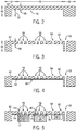
- FIGS. 2-9 a technique for manufacturing an electronics package 40 is set forth, according to an embodiment of the invention.
- a cross-section of the build-up process for a singular electronics package 40 is shown in each of FIGS. 2-9 for ease of visualization of the build-up process, however, one skilled in the art will recognize that multiple electronics packages could be manufactured in a similar manner at the panel level and then singulated into individual electronics package components as desired.
- each of the electronics packages may contain a single die, multiple die, or a combination of one or more die, chips, and passive devices.
- dielectric layer 42 that is provided in the form of a rigid or flexible glass substrate, with the rigidity/flexibility of the substrate being controllable based on a thickness, composition and manufacturing method thereof.
- dielectric layer 42 has a coefficient of thermal expansion within a range of approximately 3-9 ppm/°C.
- dielectric layer 42 has a non-planar geometry and multiple thicknesses, with the outer portion 44 of the dielectric layer 42 having a thickness 46 that is larger than the thickness 48 of the interior portion 50 of the dielectric layer 42.
- thickness 48 is approximately 50 microns, although it is recognized that thicknesses of between 25 and 150 microns would be suitable.
- dielectric layer 14 may also be provided having a constant thickness, according to alternative embodiments.
- dielectric layer 42 is formed by bonding two layers of glass via a glass-frit bond or other joining method, with an upper layer having thickness 48 and a lower layer of glass having thickness 52.
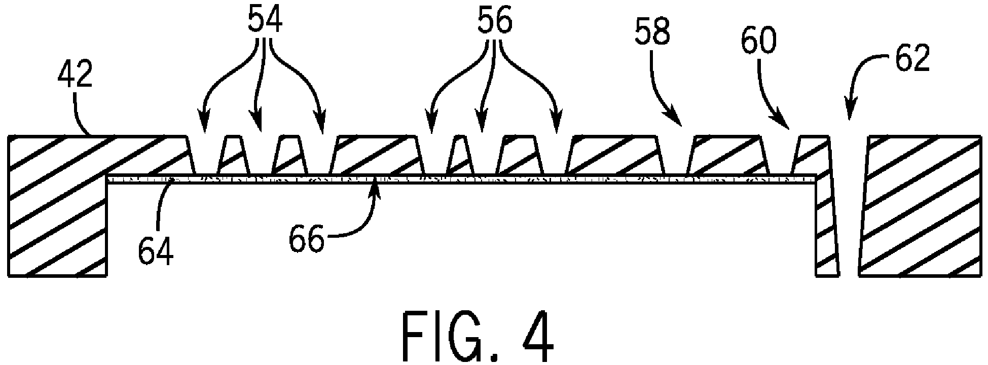
- a number of vias 54, 56, 58, 60 are formed through the interior portion 50 of dielectric layer 42 though thickness 48, as shown in FIG. 3 .
- One or more vias 62 may also be formed through the outer portion 44 of dielectric layer 42.
- Vias 54, 62 may be formed by UV laser drilling or etching, for example.
- vias 54, 62 may be formed by way of other methods including: plasma etching, dry and wet etching techniques, other laser techniques like CO2 and excimer, or mechanical drilling processes.
- vias 50, 62 are formed having angled side surfaces, as shown in FIG. 3 , which facilitates later filling and metal deposition.
- an adhesive layer 64 is applied to the bottom surface 66 of the interior portion 50 of dielectric layer 42, as shown in FIG. 4 .
- adhesive layer 64 is applied such that it coats the entirety of the bottom surface 66.
- adhesive layer 64 may be applied to coat only select portions of the bottom surface 66.
- Adhesive layer 64 may be applied using a coating technique such as spin coating or slot die coating, or may be applied by a programmable dispensing tool in the form of an inkjet printing-type device technique, as non-limiting examples.
- Adhesive layer 64 is a high temperature adhesive such as, for example, a high temperature polyimide, epoxies, cyanate ester material, or a blend thereof, that is suitable for use at temperatures of 150 °C at a lower limit and 250 °C at an upper limit. It is recognized that other adhesives could also be implemented that are suitable for use at temperatures greater than 250 °C, such as at 300 °C or even 400 °C, depending on the application.
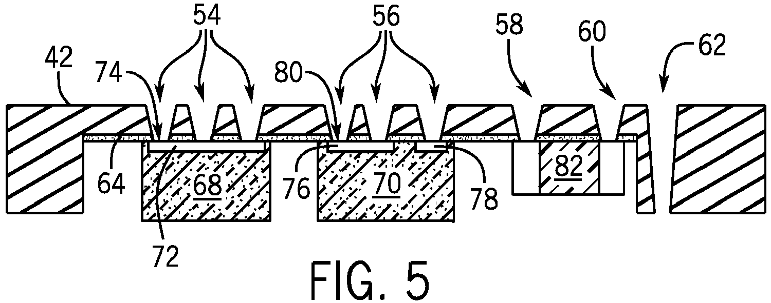
- semiconductor devices 68, 70 are coupled to adhesive layer 64.
- Semiconductor devices 68, 70 may be of the same thickness, as shown in FIG. 5 , or of varying thickness in an alternative embodiment. In one non-limiting embodiment, semiconductor devices 68, 70 have a thickness within a range of approximately 50-500 microns.
- Semiconductor devices 68, 70 may be generally described as "power devices” or “non-power devices.” Thus, semiconductor devices 68, 70 may be in the form of a die, diode, MOSFET, transistor, application specific integrated circuit (ASIC), or processor, as examples.
- ASIC application specific integrated circuit
- semiconductor device 68 is depicted as a diode having a contact pad 72 positioned on an active surface 74 thereof.
- Semiconductor device 70 is depicted as a MOSFET having a source pad 76 and gate pad 78 positioned on its active surface 80.
- semiconductor devices 68, 70 may be provided as alternative types of power or non-power devices and that a lesser or greater number of semiconductor devices or electronic components may be included within electronics package 40.
- semiconductor devices 68, 70 are formed of silicon or silicon carbide (SiC) and have a coefficient of thermal expansion within a range of approximately 2-3 ppm/°C.
- one or more passive devices 82 such as, for example, a resistor, a capacitor, or an inductor, may be placed onto adhesive layer 64.
- adhesive layer 64 may be fully cured, thermally or by a combination of heat or radiation. Suitable radiation may include UV light and/or microwaves. In one embodiment, a partial vacuum and/or above atmospheric pressure may be used to promote the removal of volatiles from the adhesive during cure if any are present.
- any portion of adhesive layer 64 beneath vias 54 is removed using, for example, a reactive ion etching (RIE) or laser process that does not significantly impact the structural integrity of the dielectric layer 42.
- RIE reactive ion etching
- a lower metallization layer 84 is formed on a lower surface 86 of the outer portion 44 of dielectric layer 42 in a next step of the fabrication process. Following the application process, a portion of metallization layer 84 may extend up into via 62 as shown.
- An upper metallization layer 88 is formed on the upper surface 90 of dielectric layer 42, as shown in FIG. 7 . Upper metallization layer 88 extends through vias 54 to electrically couple with contact pads 72, 76, 78 of semiconductor devices 68, 70. Upper metallization layer 88 also extends through vias 62 to electrically couple with lower metallization layer 84.
- the upper metallization layer 88 and lower metallization layer 84 thus form electrical connections between the lower surface 86 and the upper surface 90 of dielectric layer 42.
- an optional titanium-copper seed layer (not shown) is sputter-plated onto the upper surface 90 and/or lower surface 86 of dielectric layer 42 prior to deposition of upper and lower metallization layers 84, 90.
- Metallization layers 84, 90 may be formed using a sputtering and plating technique, followed by a lithography process. In one embodiment, lower and upper metallization layers 84, 90 are formed of copper. However, it is contemplated that the manufacturing technique of metallization layers 84, 90 may be extended to the use of other electrically conducting materials or a combination of copper and a filling agent. In embodiments that do not include passive device 82, gate pad 78 of semiconductor device 70 may be electrically coupled to lower metallization layer 84 through an extension of upper metallization layer 88 (not shown in FIG. 7 ) that is coupled to lower metallization layer 84 through via 62.
- First joining layer 92 is applied to the respective bottom surfaces 94, 96 of semiconductor devices 68, 70 and to a portion of lower metallization layer 84 aligned with via(s) 62.
- First joining layer 92 is formed of solder or other high temperature joining material such as sintered silver or other alloys/intermetallics formed using a transient liquid phase bonding technique, with solder such as 92.5Pb/5Sn/2.5Ag or Au-Si being an example of a suitable material.
- a second joining layer 98 or other high temperature, near-hermetic (i.e., having a helium leak rate of 1E-4 to 1E-6 atm-cc/sec) joining material is applied to lower metallization layer 84 to form a continuous path that surrounds the interior portion 50 of dielectric layer 42.
- second joining layer 98 may be an electrically conductive material or electrically insulative material such as, for example, sintered silver, a transient liquid phase bonding material, or low temperature glass or polymeric systems that exhibit low moisture absorption and diffusion rates (for example, liquid crystalline polymers).
- solder is used for second joining layer 98, the bottom surface of the exterior portion of the dielectric layer 42 is metallized.
- an optional finish layer (not shown) is provided on the lower metallization layer 84 prior to application of the second joining layer 98.
- a Ni-Au finish may be used when second joining layer 98 is solder and a Ni-Ag finish may be used when second joining layer 98 is sintered silver.
- the first and second joining layers 92, 98 may be formed of the same material.
- a conductive substrate 100 is coupled to the first and second joining layers 92, 98 using an appropriate welding or bonding process to form an electronics package 40, as shown in FIG. 9 .
- conductive substrate 100 is a multi-layer substrate 100 that includes a layer of ceramic substrate 102, such as, for example, alumina, sandwiched between upper and lower sheets 104, 106 formed from an electrically conductive material such as, for example, copper.
- portions of upper sheet 104 are removed to create a patterned upper surface for multi-layer substrate 100.
- first and second joining layers 92, 98 may be initially applied to the multi-layer substrate 100 rather than to the lower metallization layer 84 and semiconductor devices 68, 70.
- second joining layer 98 may be applied to directly couple multi-layer substrate 100 to dielectric layer 42 after semiconductor devices 68, 70 are coupled to multi-layer substrate 100, thereby creating an edge seal around the interior cavity 108 surrounding semiconductor devices 68, 70 and passive device(s) 82.
- the portion of lower metallization layer 84 shown positioned between dielectric layer 42 and second joining layer 98 may be omitted, as described in more detail with respect to FIG. 19 .
- multi-layer substrate 100 is a direct bond copper (DBC) substrate.
- DBC direct bond copper
- substrate 100 is a metal leadframe, such as, for example, copper, that may be molded or encapsulated.
- I/O connections may be formed atop upper metallization layer 88 and/or multi-layer substrate 100 such that electrical connections may be made between the electrical components within electronics package 40 and external components (not shown) such as, for example, a busbar or printed circuit board (PCB).
- I/O connections may be provided in the form of plated bumps, pillar bumps, copper straps, Cu terminals directly bonded or solder joined, or wirebond connections/pads, as non-limiting examples.
- a solder mask may be applied to support some of the I/O connection methods mentioned above.
- FIG. 10 A top view of electronics package 40 is provided in FIG. 10 to more clearly illustrate how second joining layer 98 is positioned to surround the interior portion 50 of dielectric layer 14 and semiconductor devices 68, 70 and passive device(s) 82 coupled thereto.
- second joining layer 98 hermetically seals the cavity 108 surrounding semiconductor devices 68, 70 and passive device(s) 82. Cavity 108 may then be filled with dry air, or an inert gas such as argon or nitrogen as non-limiting examples.
- second joining layer 98 is applied to surround and seal a subsection of the interior portion 50 of dielectric layer 14.
- passive device 82 may be positioned outside the hermetic seal of cavity 108 or may be omitted entirely.
- semiconductor devices 68, 70 and passive device(s) 82 may be overcoated with an encapsulant (not shown) in the form of a non-conductive material such as, for example, a polymer, that fills cavity 108.
- Encapsulant may be used, for example, in high voltage applications to prevent arcing between semiconductor devices and metal components or to provide rigidity and ease of handling.
- passive device(s) 82 may be positioned on a top surface 110 of upper metallization layer 88.
- FIG. 10 illustrates an exemplary arrangement of upper metallization layer 88 and vias 54, 56, 58, 62 with respect to semiconductor devices 68, 70 and passive device(s) 82.
- a first portion 112 of upper metallization layer 88 is positioned above vias 54 and vias 56 and, therefore electrically coupled to contact pad 72 of semiconductor device 68 and source pad 76 of semiconductor device 70.
- a second portion 114 of upper metallization layer 88 is aligned with the via 56 that is electrically coupled to gate pad 78 of semiconductor device 70 and via 58 of passive device 82.
- a third portion 116 of upper metallization layer 88 forms an electrical connection between passive device 82 and lower metallization layer 84 through via 60 and via 62.
- an electronics subpackage including dielectric layer 42, adhesive layer 64, and one or both of lower metallization layer 84 and upper metallization layer 88 may be manufactured as a pre-fabricated module with or without semiconductor devices 68, 70 and passive device(s) 82.
- adhesive layer 64 may be provided in a partially cured state (e.g., as a B-stage material) that is stable enough for further handling or transport. This will permit semiconductor devices 68, 70 and passive device(s) 82 to be subsequently attached to the electronics subpackage in a later processing step.
- adhesive layer 64 may be applied prior to formation of vias 54-62.
- lower metallization layer 84 may be formed on the lower surface 86 of dielectric layer 42 prior to positioning semiconductor devices 68, 70 and passive device 82 or even prior to application of adhesive layer 64.
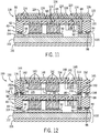
- an additional build-up layer 118 may be coupled to upper metallization layer 88, as shown in FIG. 11 .
- build-up layer 118 is formed by applying a layer of adhesive 120 to the top surface 90 of dielectric layer 42 and to upper metallization layer 88 and then placing an upper dielectric layer 122 onto adhesive 120, although it is recognized that the build-up layer 118 could be one single layer that acts as an adhesive and film to metallize or two layers - an adhesive and a non-flowing film.
- the build-up layers could be polymeric or glass.
- upper dielectric layer 122 has a uniform or substantially uniform thickness 123 throughout.
- upper dielectric layer 122 is a glass substrate having a number of vias 124 formed through a thickness thereof.
- upper dielectric layer 122 may be a polyimide material, such as Kapton for example.
- upper dielectric layer 122 may be applied as a film or lamination and later etched to form vias 124.
- a metallization layer 126 is formed on a top surface 128 of upper dielectric layer 122 and extends through vias 124 to electrically connect with upper metallization layer 88. Similar to upper metallization layer 88, metallization layer 126 may comprise an electrically conductive material such as, for example, copper, and may be formed using a sputtering and plating technique, followed by a lithography process. Additional redistribution layers may be formed atop redistribution layer 118 based on design specifications.
- FIG. 12 illustrates an alternative embodiment of an electronics package 159 having a stacked arrangement, wherein an electronics package submodule 130 including one or more semiconductor devices 132, 133 and passive devices 134 and an upper layer dielectric substrate 136 is coupled to electronics package 40.
- semiconductor device 133 is a power semiconductor device having backside connections that are electrically coupled to the upper metallization layer 88 of an optional electrically conducting shim 135 (shown in phantom).
- Upper layer dielectric substrate 136 is a glass substrate constructed in a similar manner as described above for dielectric layer 42 and is coupled to devices 132, 133, 134 by way of an adhesive layer 138.
- Upper layer dielectric substrate 136 is provided having one or more vias 140 that extend through an interior portion 142 of the substrate 136 and one or more vias 144 that extend through an outer portion 146 thereof.
- An upper metallization layer 148 and a lower metallization layer 150 are formed on respective top and bottom surfaces 152, 154 of upper layer dielectric substrate 136.
- joining layer 156 electrically connects the lower metallization layer 150 of electronics package submodule 130 to the upper metallization layer 88. Similar to first joining layer 92, joining layer 156 is solder or another electrically conductive, high temperature joining material such as, for example, sintered silver. Another joining layer 158 extends around the outer perimeter of the outer portion 146 of upper layer dielectric substrate 136 between lower metallization layer 150 of electronics package submodule 130 and upper metallization layer 88. According to alternative embodiments, either joining layer 158 or joining layer 98 is hermetic, depending on the application. In one embodiment, joining layer 158 creates a hermetic, or near-hermetic seal within the cavity 160 surrounding devices 132, 134.
- FIG. 13 An electronics package 161 is illustrated in FIG. 13 according to an alternative embodiment of the invention. Similar to electronics package 159 of FIG. 12 , electronics package 161 includes two electronics package submodules 40, 130, which are arranged in a stacked arrangement. Other common components between electronics package 161 and electronics package 159 are illustrated relative to the same reference numbers as appropriate.
- the upper layer dielectric substrate 136 includes a central post 137, which extends downward into cavity 160.
- a portion of lower metallization layer 150 is formed on a bottom surface 139 of the central post 137.
- a via 141 extends through the thickness of central post 137 and is metalized in a similar manner as via 144 to electrically connect upper metallization layer 148 to lower metallization layer 150.
- FIG. 14 illustrates an electronics package 163 according to another embodiment of the invention, which includes two electronics package submodules 41, 131 arranged in a stacked configuration.
- components common to electronics package 163 and electronics package 159 FIG. 12
- FIG. 13 electronics package submodule 131 is inverted atop electronics package submodule 41 with their opposing upper metallization layers 88 electrically connected to one another with a joining layer 156.
- Each electronics package submodule 41, 131 includes a respective thermally and electrically conductive substrate 43, 143 that is coupled to semiconductor devices 68, 70 and lower metallization layer 88 by way of joining layers 92, 98 as shown.
- either of both of conductive substrates 43, 143 may be an encapsulated metal lead frame or a multi-layer substrate such as, for example, a DBC substrate or printed circuit board (PCB).
- conductive substrate 43 is a DBC substrate and conductive substrate 143 is a PCB.
- Either or both of conductive substrates 43, 143 may further include a heat sink (not shown) to facilitate cooling of semiconductor devices 68, 70.
- a heat sink not shown
- electronics package 163 includes input/output (I/O) connections 167 (shown in phantom) and/or downward-facing I/O connections 169 (also shown in phantom), which are electrically connected to semiconductor devices 68, 70 through lower metallization layer 88.
- I/O connections 167, 169 may be configured as metal (e.g., copper) lead frame connections or other known form of I/O connection according to alternative embodiments.
- electronics package submodules 41, 131 may both be configured in a similar manner as power modules having one or more semiconductor devices 68, 70 and one or more other circuit components such as passive devices 82 as illustrated in FIG. 14 .
- electronics package submodules 41, 131 may be provided having differing configurations.
- electronics package submodule 41 may be configured as a power module in a similar manner to that illustrated in FIG. 14 while electronics package submodule 131 may be configured as a control circuit.
- electronics package 162 is shown according to an alternative embodiment.
- Electronics package 162 and electronics package 40 ( FIG. 9 ) share a number of common components, which will be discussed and illustrated relative to the same reference numbers as appropriate.
- electronics package 162 includes a dielectric layer 42 in the form of a glass substrate having an adhesive layer 64 formed on a bottom surface 66 thereof.
- Upper metallization layer 88 extends through vias 54, 58 to electrically connect to semiconductor devices 68, 70, which are coupled to adhesive layer 64.
- a portion of upper metallization layer 88 extends through via 62 and is electrically coupled with lower metallization layer 84.
- Lower metallization layer 84 extends around the perimeter of dielectric layer 42 and is coupled to multi-layer substrate 100 by way of a second joining layer 98, which may hermetically seal cavity 108 according to various embodiments.
- a first joining layer 92 couples semiconductor devices 68, 70 and lower metallization layer 84 to multi-layer substrate 100.
- electronics package 162 includes a metallization layer 164 formed on the bottom surface 66 of the interior portion 50 of dielectric layer 42. Similar to metallization layers 84, 90, metallization layer 164 is an electrically conductive material such as, for example, copper, and may be formed using a sputtering and plating technique, followed by a lithography process.
- a joining material 168 mechanically and electrically couples passive device 82 to metallization layer 164.
- joining material 168 may be solder, sintered silver, a conductive adhesive such as a polymer filled with an electrically conductive filler such as silver, or another electrically conductive material able to withstand high temperatures.
- joining material 168 is used to couple passive device 82 to metallization layer 164 using a liquid phase bonding joining technique.
- FIG. 16 illustrates an electronics package 170 according to another alternative embodiment.
- Electronics package 170 includes similar components as electronics package 162 of FIG. 15 , except that the via 62 and portion of upper metallization layer 88 extending through via 62 of electronics package 162 is replaced by an electrically conductive shim 172 in electronics package 170.
- conductive shim 172 may be copper or another electrically conductive metallic material.
- a portion of upper metallization layer 88 extends through a via 174 formed through the thickness 48 of dielectric layer 42 and adhesive layer 64 and is coupled with conductive shim 172.
- a portion of first joining layer 92 electrically and mechanically couples conductive shim 172 to multi-layer substrate 100.
- FIGS. 17 and 18 illustrate electronics package 170 according to alternative embodiments where semiconductor devices 68, 70 are of differing heights or thicknesses.
- an electronically conductive shim 171 is provided to offset the height difference between semiconductor devices 68, 70 and is coupled to semiconductor device 70 with a layer of solder 93 or other electically condcutive joining material.
- dielectric layer 42 is provided having a central post 173 that extends downward into cavity 108.
- Semiconductor device 70 is coupled to a bottom surface 175 of central post 173 with an adhesive layer 177, similar to adhesive layer 64.
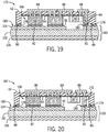
- electronics package 176 is shown according to another embodiment of the invention.
- electronics package 176 includes a number of components similar to those described with respect to electronics package 40 ( FIG. 9 ), and corresponding part numbers are referred to herein as appropriate.
- passive device 82 is shown directly coupled to adhesive layer 64 in FIG. 19 , it is contemplated that a metallization layer 164 ( FIG. 15 ) and joining material 168 ( FIG. 15 ) may be used to couple passive device 82 to dielectric layer 42 in alternative embodiments.
- the electronics package 176 shown in FIG. 19 includes a joining layer 178 that directly couples the lower surface 86 of dielectric layer 42 to the upper surface 180 of upper copper sheet 104 of multi-layer substrate 100.
- Joining layer 178 is a high temperature joining material such as, for example, glass frit or polymers that provide low diffusion characteristics - such as liquid crystalline polymers.
- joining layer 178 is applied after the semiconductor devices 68, 70 are coupled to the multi-layer substrate 100 through a dispense and cure method.
- Joining layer 178 may be applied having a filleted outward facing surface, as shown in FIG. 19 .
- FIG. 20 illustrates an electronics package 182 that includes a joining layer 178 according to an alternative embodiment of the invention.
- the lower metallization layer 84 of FIG. 9 is omitted entirely.
- Semiconductor devices 68, 70 and conductive shim 172 are directly coupled to upper copper sheet 104 of multi-layer substrate 100.
- a hermetic or near-hermetic seal is formed surrounding the perimeter of cavity 108 by applying joining layer 178 between lower surface 86 of dielectric layer 42 and upper copper sheet 104.
- joining layer 178 may be formed having a filleted outward facing surface.
- the combined use of conductive shim 172 and first joining layer 92 alleviate the need for a metallization layer similar to lower metallization layer 84 ( FIG. 9 ) on the lower surface 86 of dielectric layer 42.
- embodiments of the invention include an electronics package having a dielectric layer provided in the form of a glass substrate having a coefficient of thermal expansion that is a close match to that of the SiC or other high temperature semiconductor device(s) included within the electronics package.
- the close match between the coefficients of thermal expansion minimize heat-induced stress within the electronics package and improve package reliability, characteristics that are particularly desirable where SiC and other semiconductor devices are incorporated into the electronics package that operate at high frequencies, high voltages, and high temperatures.
- the use of the glass substrate also facilitates the fabrication of high power density electronics packages.
- one or more semiconductor devices and other electronic components may be hermetically sealed in a cavity formed between the glass substrate and multi-layer substrate.
- a hermetic environment extends the high temperature reliability of the SiC or other high temperature semiconductor devices and the adhesive that is used to attach the devices to the glass substrate.
- the ability to provide a hermetic seal also alleviates the need to provide an encapsulant or other underfill material surrounding the semiconductor devices, thereby reducing material and processing costs.
- Embodiments incorporating a multi-thickness glass substrate also provide through interconnections in the form of metalized vias through the thicker portions of the glass substrate, which replace electrically conductive shims and reduce manufacturing steps.
- an electronics package includes a glass substrate having an exterior portion surrounding an interior portion thereof, wherein the interior portion has a first thickness and the exterior portion has a second thickness larger than the first thickness.
- the electronics package further includes an adhesive layer formed on a lower surface of the interior portion of the glass substrate and a semiconductor device having an upper surface coupled to the adhesive layer, the semiconductor device having at least one contact pad disposed on the upper surface thereof.
- a first metallization layer is coupled to an upper surface of the glass substrate and extends through a first via formed through the first thickness of the glass substrate to couple with the at least one contact pad of the semiconductor device.
- a method of manufacturing an electronics package includes providing a glass substrate having an interior portion surrounded by an exterior portion, the exterior portion having a thickness greater than a thickness of the interior portion.
- the method also includes forming an adhesive layer on a lower surface of the interior portion of the glass substrate, coupling an upper surface of a semiconductor device to the glass substrate by way of the adhesive layer, the upper surface comprising at least one contact pad, and forming a first metallization layer on the glass substrate, the first metallization layer extending through at least one via formed through the thickness of the interior portion of the glass substrate to connect to the at least one contact pad of the semiconductor device.
- a power electronics package includes a multi-thickness substrate having at least one via formed through a first thickness thereof and a power device having an active surface coupled to the multi-thickness substrate, the active surface comprising at least one contact pad aligned with the at least one via in the multi-thickness substrate.
- a first metallization layer is formed on an upper surface of the multi-thickness substrate and extends through the at least one via to contact the at least one contact pad. The difference between the coefficient of thermal expansion of the multi-layer substrate and the coefficient of thermal expansion of the power device is less than approximately 7 ppm/°C.
Landscapes
- Structures Or Materials For Encapsulating Or Coating Semiconductor Devices Or Solid State Devices (AREA)
Abstract
Description
- Embodiments of the invention relate generally to semiconductor device packages or electronics packages and, more particularly, to a power electronics package that includes an interconnect structure formed of a glass dielectric material.
- Power semiconductor devices are semiconductor devices used as switches or rectifiers in power electronic circuits, such as switched mode power supplies, for example. Many power semiconductor devices are used in high voltage power applications and are designed to carry a large amount of current and support a large voltage.
- In use, power semiconductor devices are typically mounted to an external circuit by way of a packaging structure, with the packaging structure providing an electrical connection to the external circuit and also providing a way to remove the heat generated by the devices and protect the devices from the external environment. Power semiconductor devices are provided with a number of input/output (I/O) interconnections to electrically connect both sides of a respective semiconductor device to an external circuit. These I/O connections may be provided in the form of solder balls, plated bumps, or wirebond connections. In the case of wirebond packaging, wirebonds are provided that connect bond pads or contact pads provided on the power semiconductor device to a corresponding pad or conductive element at the next level of packaging, which may be a circuit board or leadframe. Most existing power device packaging structures use a combination of wirebonds and a substrate (e.g., a direct bonded copper (DBC) substrate) to provide I/O interconnections to both sides of a respective semiconductor device.
- As semiconductor device packages have become increasingly smaller and yield better operating performance, packaging technology has correspondingly evolved from leaded packages to planar build-up packages that incorporate buried or embedded semiconductor devices. The general structure of a prior art
planar packaging structure 10 incorporating an embedded power device is shown inFIG. 1 . The standard manufacturing process for thePOL structure 10 typically begins with placement of one or morepower semiconductor devices 12 onto adielectric layer 14 by way of an adhesive 16 that is applied to dielectric layer using a spin coating technique.POL structure 10 may also include one or more additional die packages, packaged controllers, or other electrical components such as inductors orpassive components 18.Dielectric layer 14 is a polyimide or other organic material, such as Kapton for example, which has a coefficient of thermal expansion of approximately 20 ppm/°C.Dielectric layer 14 is provided as a planar prefabricated film or lamination or is formed as a planar layer atop a frame structure (not shown). - Metal interconnects 20 (e.g., copper interconnects) are then electroplated onto
dielectric layer 14 to form a direct metallic connection to thepower semiconductor devices 12. Themetal interconnects 20 may be in the form of a low profile (e.g., less than 200 micrometers thick), planar interconnect structure that provides for formation of an input/output (I/O)system 22 to and from thepower semiconductor devices 12. -
POL structure 10 also includes a direct bond copper (DBC)substrate 24, which is typically formed from a non-organicceramic substrate 26 such as, for example, alumina, with upper and lower sheets ofcopper braze layer 32. Theupper copper sheet 28 ofDBC substrate 24 is patterned to form a number of conductive contact areas beforeDBC substrate 24 is attached tosemiconductor devices 12. An electricallyconductive shim 34 is provided to electrically couple a portion ofmetal interconnects 20 toDBC substrate 24. - During the fabrication process of
POL structure 10,solder 36 is applied to the surfaces ofsemiconductor devices 12 andshim 34.DBC substrate 24 is then lowered ontosolder 36 to align the patterned portions oflower copper sheet 30 withsolder 36. AfterDBC substrate 24 is coupled tosemiconductor devices 12 andshim 34, an underfill technique is used to apply a polymericdielectric material 38 in the space betweenadhesive layer 16 andDBC substrate 24. While polymericdielectric material 38 provides some environmental protection forsemicondcutor devices 12, the semiconductor devices are not hermetically sealed due to the inherent characteristic of thepolymeric material 38 that allows moisture and other gases to diffuse through it. - Advancements in semiconductor chip packaging technology are driven by ever-increasing needs for achieving better performance, greater miniaturization, and higher reliability. Such advancements have led to the development of new semiconductor technologies such as, for example, silicon carbide (SiC) power devices. These new power devices may be operated to switch at high frequencies and at high voltages. However, these devices also operate at elevated temperatures as compared to prior art devices, i.e., at temperatures above 150 °C, with temperatures typically in the range of 150 to 250 °C but sometimes exceeding 300 °C.
- As explained with respect to
FIG. 1 , existing planar packaging technologies use polyimide and other organic materials for the various dielectric and encapsulating layers within the package structure. While these materials may provide for a planar package structure, polyimide and other organic materials are limited in temperature and reliability at elevated temperatures, as these materials have an upper temperature limit in the range of 150 to 175 degrees Celsius. Ceramic materials such as alumina may also be incorporated into planar packaging structures. However, the high cost and brittle nature of these materials severely limit their capabilities. - To fully utilize the capabilities of these new semiconductor technologies, it would be desirable to provide a new planar packaging technology that maintains reliability at the elevated operating temperatures, frequencies, and voltages of SiC and other high temperature power devices. It would further be desirable for such a packaging technology to hermetically seal the power devices and simplify the current manufacturing process.
- In accordance with one aspect of the invention, an electronics package includes a glass substrate having an exterior portion surrounding an interior portion thereof, wherein the interior portion has a first thickness and the exterior portion has a second thickness larger than the first thickness. The electronics package further includes an adhesive layer formed on a lower surface of the interior portion of the glass substrate and a semiconductor device having an upper surface coupled to the adhesive layer, the semiconductor device having at least one contact pad disposed on the upper surface thereof. A first metallization layer is coupled to an upper surface of the glass substrate and extends through a first via formed through the first thickness of the glass substrate to couple with the at least one contact pad of the semiconductor device.
- In accordance with another aspect of the invention, a method of manufacturing an electronics package includes providing a glass substrate having an interior portion surrounded by an exterior portion, the exterior portion having a thickness greater than a thickness of the interior portion. The method also includes forming an adhesive layer on a lower surface of the interior portion of the glass substrate, coupling an upper surface of a semiconductor device to the glass substrate by way of the adhesive layer, the upper surface comprising at least one contact pad, and forming a first metallization layer on the glass substrate, the first metallization layer extending through at least one via formed through the thickness of the interior portion of the glass substrate to connect to the at least one contact pad of the semiconductor device.
- In accordance with yet another aspect of the invention, a power electronics package includes a multi-thickness substrate having at least one via formed through a first thickness thereof and a power device having an active surface coupled to the multi-thickness substrate, the active surface comprising at least one contact pad aligned with the at least one via in the multi-thickness substrate. A first metallization layer is formed on an upper surface of the multi-thickness substrate and extends through the at least one via to contact the at least one contact pad. The difference between the coefficient of thermal expansion of the multi-layer substrate and the coefficient of thermal expansion of the power device is less than approximately 7 ppm/°C.
- These and other advantages and features will be more readily understood from the following detailed description of preferred embodiments of the invention that is provided in connection with the accompanying drawings.
- The drawings illustrate embodiments presently contemplated for carrying out the invention.
- In the drawings:
-
FIG. 1 is a schematic cross-sectional side view of a prior art electronics package incorporating a power device. -
FIGS. 2-9 are schematic cross-sectional side views of an electronics package during various stages of a manufacturing/build-up process according to an embodiment of the invention. -
FIG. 10 is a schematic top view of an electronics package manufactured according to the process illustrated inFIGS. 2-9 . -
FIG. 11 is a schematic cross-sectional side view of an electronics package according to another embodiment of the invention. -
FIG. 12 is a schematic cross-sectional side view of an electronics package according to another embodiment of the invention. -
FIG. 13 is a schematic cross-sectional side view of an electronics package according to another embodiment of the invention. -
FIG. 14 is a schematic cross-sectional side view of an electronics package according to another embodiment of the invention. -
FIG. 15 is a schematic cross-sectional side view of an electronics package according to yet another embodiment of the invention. -
FIG. 16 is a schematic cross-sectional side view of an electronics package according to yet another embodiment of the invention. -
FIG. 17 is a schematic cross-sectional side view of an electronics package according to yet another embodiment of the invention. -
FIG. 18 is a schematic cross-sectional side view of an electronics package according to yet another embodiment of the invention. -
FIG. 19 is a schematic cross-sectional side view of an electronics package according to yet another embodiment of the invention. -
FIG. 20 is a schematic cross-sectional side view of an electronics package according to yet another embodiment of the invention. - Embodiments of the present invention provide for a method of forming an electronics package that includes a glass substrate having a coefficient of thermal expansion that can be controlled through its composition and that more closely matches that of the semiconductor devices or electronics components than conventional polymeric substrates. Use of the disclosed glass substrate also permits hermeticity or near hermeticity for the devices or components. Embodiments described herein also provide the ability to fully utilize the capability of new semiconductor technologies, such as SiC, and their ability to switch at high frequencies at high voltages and temperatures.
- Embodiments of the invention are directed to an electronics package that includes one or more semiconductor devices, dies, or chips embedded within the electronics package. While the semiconductor devices embedded in the electronics package are referenced below in the embodiments of
FIGS. 2-20 specifically as power devices, it is understood that other electrical components could be substituted in the electronics package, and thus embodiments of the invention are not limited only to the embedding of power devices in an electronics package. That is, the use of power devices in the electronics package embodiments described below should also be understood to encompass other electrical components such as resistors, capacitors, inductors, filters, or other similar devices, that could be provided in the electronics package either alone or in combination with one or more power devices. Additionally, while the embodiments ofFIGS. 2-20 are described as including two power devices and one passive device, it is contemplated that the concepts described herein may be extended to electronics packages that include a single semiconductor device or passive device and to electronics packages that include any other number of semiconductor devices or passive devices, either alone or in combination. - Referring now to
FIGS. 2-9 , a technique for manufacturing anelectronics package 40 is set forth, according to an embodiment of the invention. A cross-section of the build-up process for asingular electronics package 40 is shown in each ofFIGS. 2-9 for ease of visualization of the build-up process, however, one skilled in the art will recognize that multiple electronics packages could be manufactured in a similar manner at the panel level and then singulated into individual electronics package components as desired. Also, each of the electronics packages may contain a single die, multiple die, or a combination of one or more die, chips, and passive devices. - Fabrication of
electronics package 40 begins with adielectric layer 42 that is provided in the form of a rigid or flexible glass substrate, with the rigidity/flexibility of the substrate being controllable based on a thickness, composition and manufacturing method thereof. According to various embodiments,dielectric layer 42 has a coefficient of thermal expansion within a range of approximately 3-9 ppm/°C. As showndielectric layer 42 has a non-planar geometry and multiple thicknesses, with theouter portion 44 of thedielectric layer 42 having athickness 46 that is larger than thethickness 48 of theinterior portion 50 of thedielectric layer 42. In one non-limiting embodiment,thickness 48 is approximately 50 microns, although it is recognized that thicknesses of between 25 and 150 microns would be suitable. As shown, arecess 51 is formed between theouter portion 44 and theinterior portion 50 of thedielectric layer 42 as a result of the difference in thickness of the twoportions dielectric layer 14 may also be provided having a constant thickness, according to alternative embodiments. In yet another embodiment,dielectric layer 42 is formed by bonding two layers of glass via a glass-frit bond or other joining method, with an upperlayer having thickness 48 and a lower layer ofglass having thickness 52. - A number of
vias interior portion 50 ofdielectric layer 42 thoughthickness 48, as shown inFIG. 3 . One ormore vias 62 may also be formed through theouter portion 44 ofdielectric layer 42.Vias FIG. 3 , which facilitates later filling and metal deposition. - In a next step of the manufacturing process, an
adhesive layer 64 is applied to thebottom surface 66 of theinterior portion 50 ofdielectric layer 42, as shown inFIG. 4 . According to the illustrated embodiment,adhesive layer 64 is applied such that it coats the entirety of thebottom surface 66. In alternative embodiments,adhesive layer 64 may be applied to coat only select portions of thebottom surface 66.Adhesive layer 64 may be applied using a coating technique such as spin coating or slot die coating, or may be applied by a programmable dispensing tool in the form of an inkjet printing-type device technique, as non-limiting examples.Adhesive layer 64 is a high temperature adhesive such as, for example, a high temperature polyimide, epoxies, cyanate ester material, or a blend thereof, that is suitable for use at temperatures of 150 °C at a lower limit and 250 °C at an upper limit. It is recognized that other adhesives could also be implemented that are suitable for use at temperatures greater than 250 °C, such as at 300 °C or even 400 °C, depending on the application. - Referring to
FIG. 5 , one ormore semiconductor devices adhesive layer 64.Semiconductor devices FIG. 5 , or of varying thickness in an alternative embodiment. In one non-limiting embodiment,semiconductor devices Semiconductor devices semiconductor devices semiconductor device 68 is depicted as a diode having acontact pad 72 positioned on anactive surface 74 thereof.Semiconductor device 70 is depicted as a MOSFET having asource pad 76 andgate pad 78 positioned on itsactive surface 80. However, it is recognized thatsemiconductor devices electronics package 40. In one embodiment,semiconductor devices passive devices 82, such as, for example, a resistor, a capacitor, or an inductor, may be placed ontoadhesive layer 64. Aftersemiconductor devices adhesive layer 64 may be fully cured, thermally or by a combination of heat or radiation. Suitable radiation may include UV light and/or microwaves. In one embodiment, a partial vacuum and/or above atmospheric pressure may be used to promote the removal of volatiles from the adhesive during cure if any are present. Once cured, any portion ofadhesive layer 64 beneathvias 54 is removed using, for example, a reactive ion etching (RIE) or laser process that does not significantly impact the structural integrity of thedielectric layer 42. - As shown in
FIG. 6 , alower metallization layer 84 is formed on alower surface 86 of theouter portion 44 ofdielectric layer 42 in a next step of the fabrication process. Following the application process, a portion ofmetallization layer 84 may extend up into via 62 as shown. Anupper metallization layer 88 is formed on theupper surface 90 ofdielectric layer 42, as shown inFIG. 7 .Upper metallization layer 88 extends throughvias 54 to electrically couple withcontact pads semiconductor devices Upper metallization layer 88 also extends throughvias 62 to electrically couple withlower metallization layer 84. Together, theupper metallization layer 88 andlower metallization layer 84 thus form electrical connections between thelower surface 86 and theupper surface 90 ofdielectric layer 42. In one embodiment, an optional titanium-copper seed layer (not shown) is sputter-plated onto theupper surface 90 and/orlower surface 86 ofdielectric layer 42 prior to deposition of upper and lower metallization layers 84, 90. - Metallization layers 84, 90 may be formed using a sputtering and plating technique, followed by a lithography process. In one embodiment, lower and upper metallization layers 84, 90 are formed of copper. However, it is contemplated that the manufacturing technique of metallization layers 84, 90 may be extended to the use of other electrically conducting materials or a combination of copper and a filling agent. In embodiments that do not include
passive device 82,gate pad 78 ofsemiconductor device 70 may be electrically coupled tolower metallization layer 84 through an extension of upper metallization layer 88 (not shown inFIG. 7 ) that is coupled tolower metallization layer 84 through via 62. - Referring now to
FIG. 8 , a first joininglayer 92 is applied to the respective bottom surfaces 94, 96 ofsemiconductor devices lower metallization layer 84 aligned with via(s) 62. First joininglayer 92 is formed of solder or other high temperature joining material such as sintered silver or other alloys/intermetallics formed using a transient liquid phase bonding technique, with solder such as 92.5Pb/5Sn/2.5Ag or Au-Si being an example of a suitable material. A second joininglayer 98 or other high temperature, near-hermetic (i.e., having a helium leak rate of 1E-4 to 1E-6 atm-cc/sec) joining material is applied tolower metallization layer 84 to form a continuous path that surrounds theinterior portion 50 ofdielectric layer 42. According to various embodiments, second joininglayer 98 may be an electrically conductive material or electrically insulative material such as, for example, sintered silver, a transient liquid phase bonding material, or low temperature glass or polymeric systems that exhibit low moisture absorption and diffusion rates (for example, liquid crystalline polymers). When solder is used for second joininglayer 98, the bottom surface of the exterior portion of thedielectric layer 42 is metallized. - In some embodiments an optional finish layer (not shown) is provided on the
lower metallization layer 84 prior to application of the second joininglayer 98. As non-limiting examples, a Ni-Au finish may be used when second joininglayer 98 is solder and a Ni-Ag finish may be used when second joininglayer 98 is sintered silver. In embodiments where the bottom surfaces ofsemiconductive devices layers - Next, a
conductive substrate 100 is coupled to the first and second joininglayers electronics package 40, as shown inFIG. 9 . In the illustrated embodiment,conductive substrate 100 is amulti-layer substrate 100 that includes a layer ofceramic substrate 102, such as, for example, alumina, sandwiched between upper andlower sheets FIG. 9 , portions ofupper sheet 104 are removed to create a patterned upper surface formulti-layer substrate 100. In an alternative embodiment, either or both of first and second joininglayers multi-layer substrate 100 rather than to thelower metallization layer 84 andsemiconductor devices layer 98 may be applied to directly couplemulti-layer substrate 100 todielectric layer 42 aftersemiconductor devices multi-layer substrate 100, thereby creating an edge seal around theinterior cavity 108 surroundingsemiconductor devices lower metallization layer 84 shown positioned betweendielectric layer 42 and second joininglayer 98 may be omitted, as described in more detail with respect toFIG. 19 . According to one embodiment,multi-layer substrate 100 is a direct bond copper (DBC) substrate. In an alternative embodiments,substrate 100 is a metal leadframe, such as, for example, copper, that may be molded or encapsulated. - While not shown in
FIG. 9 , it is contemplated that any number of input/output (I/O) connections may be formed atopupper metallization layer 88 and/ormulti-layer substrate 100 such that electrical connections may be made between the electrical components withinelectronics package 40 and external components (not shown) such as, for example, a busbar or printed circuit board (PCB). Such I/O connections may be provided in the form of plated bumps, pillar bumps, copper straps, Cu terminals directly bonded or solder joined, or wirebond connections/pads, as non-limiting examples. A solder mask may be applied to support some of the I/O connection methods mentioned above. - A top view of
electronics package 40 is provided inFIG. 10 to more clearly illustrate how second joininglayer 98 is positioned to surround theinterior portion 50 ofdielectric layer 14 andsemiconductor devices layer 98 hermetically seals thecavity 108 surroundingsemiconductor devices Cavity 108 may then be filled with dry air, or an inert gas such as argon or nitrogen as non-limiting examples. In alternative embodiments, second joininglayer 98 is applied to surround and seal a subsection of theinterior portion 50 ofdielectric layer 14. For example,passive device 82 may be positioned outside the hermetic seal ofcavity 108 or may be omitted entirely. - In embodiments where second joining
layer 98 does not hermetically sealcavity 108,semiconductor devices cavity 108. Encapsulant may be used, for example, in high voltage applications to prevent arcing between semiconductor devices and metal components or to provide rigidity and ease of handling. In another alternative embodiment, passive device(s) 82 may be positioned on atop surface 110 ofupper metallization layer 88. -
FIG. 10 illustrates an exemplary arrangement ofupper metallization layer 88 andvias semiconductor devices first portion 112 ofupper metallization layer 88 is positioned abovevias 54 andvias 56 and, therefore electrically coupled to contactpad 72 ofsemiconductor device 68 andsource pad 76 ofsemiconductor device 70. Asecond portion 114 ofupper metallization layer 88 is aligned with the via 56 that is electrically coupled togate pad 78 ofsemiconductor device 70 and via 58 ofpassive device 82. Likewise, athird portion 116 ofupper metallization layer 88 forms an electrical connection betweenpassive device 82 andlower metallization layer 84 through via 60 and via 62. - It is contemplated that an electronics subpackage including
dielectric layer 42,adhesive layer 64, and one or both oflower metallization layer 84 andupper metallization layer 88 may be manufactured as a pre-fabricated module with or withoutsemiconductor devices semiconductor devices adhesive layer 64 may be provided in a partially cured state (e.g., as a B-stage material) that is stable enough for further handling or transport. This will permitsemiconductor devices - The order and sequence the process or method steps associated with the above-described manufacturing or build-up technique of
electronics package 40 may be varied according to alternative embodiments. As one non-limiting example,adhesive layer 64 may be applied prior to formation of vias 54-62. Additionally,lower metallization layer 84 may be formed on thelower surface 86 ofdielectric layer 42 prior topositioning semiconductor devices passive device 82 or even prior to application ofadhesive layer 64. - Optionally, an additional build-
up layer 118 may be coupled toupper metallization layer 88, as shown inFIG. 11 . In one embodiment, build-up layer 118 is formed by applying a layer of adhesive 120 to thetop surface 90 ofdielectric layer 42 and toupper metallization layer 88 and then placing anupper dielectric layer 122 onto adhesive 120, although it is recognized that the build-up layer 118 could be one single layer that acts as an adhesive and film to metallize or two layers - an adhesive and a non-flowing film. The build-up layers could be polymeric or glass. In the illustrated embodiment,upper dielectric layer 122 has a uniform or substantiallyuniform thickness 123 throughout. Similar todielectric layer 42,upper dielectric layer 122 is a glass substrate having a number ofvias 124 formed through a thickness thereof. In an alternative embodiment,upper dielectric layer 122 may be a polyimide material, such as Kapton for example. In such an alternative embodiment,upper dielectric layer 122 may be applied as a film or lamination and later etched to formvias 124. - A
metallization layer 126 is formed on atop surface 128 of upperdielectric layer 122 and extends throughvias 124 to electrically connect withupper metallization layer 88. Similar toupper metallization layer 88,metallization layer 126 may comprise an electrically conductive material such as, for example, copper, and may be formed using a sputtering and plating technique, followed by a lithography process. Additional redistribution layers may be formed atopredistribution layer 118 based on design specifications. -
FIG. 12 illustrates an alternative embodiment of anelectronics package 159 having a stacked arrangement, wherein anelectronics package submodule 130 including one ormore semiconductor devices passive devices 134 and an upper layerdielectric substrate 136 is coupled toelectronics package 40. In one embodiment,semiconductor device 133 is a power semiconductor device having backside connections that are electrically coupled to theupper metallization layer 88 of an optional electrically conducting shim 135 (shown in phantom). Upperlayer dielectric substrate 136 is a glass substrate constructed in a similar manner as described above fordielectric layer 42 and is coupled todevices adhesive layer 138. Upperlayer dielectric substrate 136 is provided having one ormore vias 140 that extend through aninterior portion 142 of thesubstrate 136 and one ormore vias 144 that extend through anouter portion 146 thereof. Anupper metallization layer 148 and alower metallization layer 150, similar toupper metallization layer 88 andlower metallization layer 84, are formed on respective top andbottom surfaces dielectric substrate 136. - A joining
layer 156 electrically connects thelower metallization layer 150 ofelectronics package submodule 130 to theupper metallization layer 88. Similar to first joininglayer 92, joininglayer 156 is solder or another electrically conductive, high temperature joining material such as, for example, sintered silver. Another joininglayer 158 extends around the outer perimeter of theouter portion 146 of upper layerdielectric substrate 136 betweenlower metallization layer 150 ofelectronics package submodule 130 andupper metallization layer 88. According to alternative embodiments, either joininglayer 158 or joininglayer 98 is hermetic, depending on the application. In one embodiment, joininglayer 158 creates a hermetic, or near-hermetic seal within thecavity 160 surroundingdevices - An
electronics package 161 is illustrated inFIG. 13 according to an alternative embodiment of the invention. Similar toelectronics package 159 ofFIG. 12 ,electronics package 161 includes twoelectronics package submodules electronics package 161 andelectronics package 159 are illustrated relative to the same reference numbers as appropriate. In the embodiment ofFIG. 13 , the upper layerdielectric substrate 136 includes acentral post 137, which extends downward intocavity 160. A portion oflower metallization layer 150 is formed on abottom surface 139 of thecentral post 137. A via 141 extends through the thickness ofcentral post 137 and is metalized in a similar manner as via 144 to electrically connectupper metallization layer 148 tolower metallization layer 150. -
FIG. 14 illustrates anelectronics package 163 according to another embodiment of the invention, which includes twoelectronics package submodules electronics package 163 and electronics package 159 (FIG. 12 ) are referenced with the common reference numbers as appropriate. As shown inFIG. 13 ,electronics package submodule 131 is inverted atopelectronics package submodule 41 with their opposing upper metallization layers 88 electrically connected to one another with a joininglayer 156. Eachelectronics package submodule conductive substrate semiconductor devices lower metallization layer 88 by way of joininglayers conductive substrates conductive substrate 43 is a DBC substrate andconductive substrate 143 is a PCB. Either or both ofconductive substrates semiconductor devices semiconductor devices electronics package 163. Optionally,electronics package 163 includes input/output (I/O) connections 167 (shown in phantom) and/or downward-facing I/O connections 169 (also shown in phantom), which are electrically connected tosemiconductor devices lower metallization layer 88. I/O connections - According to various embodiments,
electronics package submodules more semiconductor devices passive devices 82 as illustrated inFIG. 14 . In alternative embodiments,electronics package submodules electronics package submodule 41 may be configured as a power module in a similar manner to that illustrated inFIG. 14 whileelectronics package submodule 131 may be configured as a control circuit. - Referring now to
FIG. 15 , anelectronics package 162 is shown according to an alternative embodiment.Electronics package 162 and electronics package 40 (FIG. 9 ) share a number of common components, which will be discussed and illustrated relative to the same reference numbers as appropriate. Similar toelectronics package 40,electronics package 162 includes adielectric layer 42 in the form of a glass substrate having anadhesive layer 64 formed on abottom surface 66 thereof.Upper metallization layer 88 extends throughvias semiconductor devices adhesive layer 64. A portion ofupper metallization layer 88 extends through via 62 and is electrically coupled withlower metallization layer 84.Lower metallization layer 84 extends around the perimeter ofdielectric layer 42 and is coupled tomulti-layer substrate 100 by way of a second joininglayer 98, which may hermetically sealcavity 108 according to various embodiments. A first joininglayer 92couples semiconductor devices lower metallization layer 84 tomulti-layer substrate 100. - In addition to the components common to electronics package 40 (
FIG. 9 ),electronics package 162 includes ametallization layer 164 formed on thebottom surface 66 of theinterior portion 50 ofdielectric layer 42. Similar to metallization layers 84, 90,metallization layer 164 is an electrically conductive material such as, for example, copper, and may be formed using a sputtering and plating technique, followed by a lithography process. A joiningmaterial 168 mechanically and electrically couplespassive device 82 tometallization layer 164. According to various embodiments, joiningmaterial 168 may be solder, sintered silver, a conductive adhesive such as a polymer filled with an electrically conductive filler such as silver, or another electrically conductive material able to withstand high temperatures. In one embodiment, joiningmaterial 168 is used to couplepassive device 82 tometallization layer 164 using a liquid phase bonding joining technique. -
FIG. 16 illustrates anelectronics package 170 according to another alternative embodiment.Electronics package 170 includes similar components aselectronics package 162 ofFIG. 15 , except that the via 62 and portion ofupper metallization layer 88 extending through via 62 ofelectronics package 162 is replaced by an electricallyconductive shim 172 inelectronics package 170. According to various embodiments,conductive shim 172 may be copper or another electrically conductive metallic material. As shown inFIG. 16 , a portion ofupper metallization layer 88 extends through a via 174 formed through thethickness 48 ofdielectric layer 42 andadhesive layer 64 and is coupled withconductive shim 172. A portion of first joininglayer 92 electrically and mechanically couplesconductive shim 172 tomulti-layer substrate 100. -
FIGS. 17 and 18 illustrateelectronics package 170 according to alternative embodiments wheresemiconductor devices FIG. 17 , an electronically conductive shim 171 is provided to offset the height difference betweensemiconductor devices semiconductor device 70 with a layer ofsolder 93 or other electically condcutive joining material. In the embodiment illustrated inFIG. 18 ,dielectric layer 42 is provided having acentral post 173 that extends downward intocavity 108.Semiconductor device 70 is coupled to abottom surface 175 ofcentral post 173 with anadhesive layer 177, similar toadhesive layer 64. - Referring now to
FIG. 19 , anelectronics package 176 is shown according to another embodiment of the invention. Again,electronics package 176 includes a number of components similar to those described with respect to electronics package 40 (FIG. 9 ), and corresponding part numbers are referred to herein as appropriate. Whilepassive device 82 is shown directly coupled toadhesive layer 64 inFIG. 19 , it is contemplated that a metallization layer 164 (FIG. 15 ) and joining material 168 (FIG. 15 ) may be used to couplepassive device 82 todielectric layer 42 in alternative embodiments. - In addition to the components common to electronics package 40 (
FIG. 9 ), theelectronics package 176 shown inFIG. 19 includes a joininglayer 178 that directly couples thelower surface 86 ofdielectric layer 42 to theupper surface 180 ofupper copper sheet 104 ofmulti-layer substrate 100. Joininglayer 178 is a high temperature joining material such as, for example, glass frit or polymers that provide low diffusion characteristics - such as liquid crystalline polymers. In one embodiment, joininglayer 178 is applied after thesemiconductor devices multi-layer substrate 100 through a dispense and cure method. Joininglayer 178 may be applied having a filleted outward facing surface, as shown inFIG. 19 . -
FIG. 20 illustrates anelectronics package 182 that includes a joininglayer 178 according to an alternative embodiment of the invention. Components common betweenelectronics package 182,electronics package 170, and electronics package 40 (FIG. 9 ) and are discussed with reference to the same part numbers as appropriate. In the embodiment ofFIG. 20 , thelower metallization layer 84 ofFIG. 9 is omitted entirely.Semiconductor devices conductive shim 172 are directly coupled toupper copper sheet 104 ofmulti-layer substrate 100. A hermetic or near-hermetic seal is formed surrounding the perimeter ofcavity 108 by applying joininglayer 178 betweenlower surface 86 ofdielectric layer 42 andupper copper sheet 104. As shown, joininglayer 178 may be formed having a filleted outward facing surface. In this embodiment the combined use ofconductive shim 172 and first joininglayer 92 alleviate the need for a metallization layer similar to lower metallization layer 84 (FIG. 9 ) on thelower surface 86 ofdielectric layer 42. - Accordingly, embodiments of the invention include an electronics package having a dielectric layer provided in the form of a glass substrate having a coefficient of thermal expansion that is a close match to that of the SiC or other high temperature semiconductor device(s) included within the electronics package. The close match between the coefficients of thermal expansion minimize heat-induced stress within the electronics package and improve package reliability, characteristics that are particularly desirable where SiC and other semiconductor devices are incorporated into the electronics package that operate at high frequencies, high voltages, and high temperatures. The use of the glass substrate also facilitates the fabrication of high power density electronics packages.
- Additionally, in embodiments where the glass substrate is provided as a multi-thickness substrate, one or more semiconductor devices and other electronic components may be hermetically sealed in a cavity formed between the glass substrate and multi-layer substrate. Such a hermetic environment extends the high temperature reliability of the SiC or other high temperature semiconductor devices and the adhesive that is used to attach the devices to the glass substrate. The ability to provide a hermetic seal also alleviates the need to provide an encapsulant or other underfill material surrounding the semiconductor devices, thereby reducing material and processing costs. Embodiments incorporating a multi-thickness glass substrate also provide through interconnections in the form of metalized vias through the thicker portions of the glass substrate, which replace electrically conductive shims and reduce manufacturing steps.
- Therefore, according to one embodiment of the invention, an electronics package includes a glass substrate having an exterior portion surrounding an interior portion thereof, wherein the interior portion has a first thickness and the exterior portion has a second thickness larger than the first thickness. The electronics package further includes an adhesive layer formed on a lower surface of the interior portion of the glass substrate and a semiconductor device having an upper surface coupled to the adhesive layer, the semiconductor device having at least one contact pad disposed on the upper surface thereof. A first metallization layer is coupled to an upper surface of the glass substrate and extends through a first via formed through the first thickness of the glass substrate to couple with the at least one contact pad of the semiconductor device.
- According to another embodiment of the invention, a method of manufacturing an electronics package includes providing a glass substrate having an interior portion surrounded by an exterior portion, the exterior portion having a thickness greater than a thickness of the interior portion. The method also includes forming an adhesive layer on a lower surface of the interior portion of the glass substrate, coupling an upper surface of a semiconductor device to the glass substrate by way of the adhesive layer, the upper surface comprising at least one contact pad, and forming a first metallization layer on the glass substrate, the first metallization layer extending through at least one via formed through the thickness of the interior portion of the glass substrate to connect to the at least one contact pad of the semiconductor device.
- According to yet another embodiment of the invention, a power electronics package includes a multi-thickness substrate having at least one via formed through a first thickness thereof and a power device having an active surface coupled to the multi-thickness substrate, the active surface comprising at least one contact pad aligned with the at least one via in the multi-thickness substrate. A first metallization layer is formed on an upper surface of the multi-thickness substrate and extends through the at least one via to contact the at least one contact pad. The difference between the coefficient of thermal expansion of the multi-layer substrate and the coefficient of thermal expansion of the power device is less than approximately 7 ppm/°C.
- While the invention has been described in detail in connection with only a limited number of embodiments, it should be readily understood that the invention is not limited to such disclosed embodiments. Rather, the invention can be modified to incorporate any number of variations, alterations, substitutions or equivalent arrangements not heretofore described, but which are commensurate with the spirit and scope of the invention. Additionally, while various embodiments of the invention have been described, it is to be understood that aspects of the invention may include only some of the described embodiments. Accordingly, the invention is not to be seen as limited by the foregoing description, but is only limited by the scope of the appended claims.
- Various aspects and embodiments of the present invention are defined by the following numbered clauses:
- 1. A power electronics package comprising:
- a multi-thickness substrate having at least one via formed through a first thickness thereof;
- a power device having an active surface coupled to the multi-thickness substrate, the active surface comprising at least one contact pad aligned with the at least one via in the multi-thickness substrate; and
- a first metallization layer formed on an upper surface of the multi-thickness substrate and extending through the at least one via to contact the at least one contact pad;
- wherein a difference between the coefficient of thermal expansion of the multi-layer substrate and the coefficient of thermal expansion of the power device is less than approximately 7 ppm/°C.
- 2. The power electronics package of
clause 1, further comprising an adhesive layer disposed between the multi-thickness substrate and the power device, the adhesive layer coupled to a portion of the multi-thickness substrate having the first thickness. - 3. The power electronics package of any preceding clause, further comprising a conductive substrate coupled to a portion of the multi-thickness substrate having a second thickness greater than the first thickness;
- wherein the power device is hermetically sealed within a cavity formed between the multi-thickness substrate and the conductive substrate.
- 4. The power electronics package of any preceding clause, further comprising:
- an electrical component coupled to the multi-thickness substrate and to the first metallization layer; and
- a second metallization layer formed on a lower surface of the portion of the multi-thickness substrate having the second thickness;
- wherein the electrical component is electrically coupled to the second metallization layer by way of a metalized via formed through the second thickness of the multi-thickness substrate.
Claims (15)
- An electronics package (40) comprising:a glass substrate (42) having an exterior portion (44) surrounding an interior portion (50) thereof, wherein the interior portion (50) has a first thickness (48) and the exterior portion (44) has a second thickness (46) larger than the first thickness (48);an adhesive layer (64) formed on a lower surface (66) of the interior portion (50) of the glass substrate (42);a semiconductor device (68, 70) having an upper surface (74) coupled to the adhesive layer (64), the semiconductor device (68, 70) having at least one contact pad (72) disposed on the upper surface (74) thereof; anda first metallization layer (88) coupled to an upper surface (90) of the glass substrate (42) and extending through a first via (54) formed through the first thickness (48) of the glass substrate (42) to couple with the at least one contact pad (72) of the semiconductor device (68, 70).
- The electronics package of claim 1, wherein a difference between the coefficient of thermal expansion of the glass substrate (42) and the coefficient of thermal expansion of the semiconductor device (68, 70) is equal to or less than 7 ppm/°C.
- The electronics package of claim 1 or 2, wherein the semiconductor device (68, 70) comprises a power device.
- The electronics package of any of claims 1 to 3, further comprising a second metallization layer (84) coupled to a lower surface (86) of the exterior portion (44) of the glass substrate;wherein the first metallization (88) layer and the second metallization layer (84) electrically connect within a second via (62) formed through the second thickness of the glass substrate.
- The electronics package of claim 4, further comprising a passive device (82) coupled to the adhesive layer (64); andwherein the passive device (82) is electrically connected to the first metallization layer (88).
- The electronics package of any of claims 1 to 5, further comprising a conductive shim (172) positioned adjacent a bottom surface of the glass substrate (42) and electrically coupled to the first metallization layer (88).
- The electronics package of any preceding claim, further comprising:a conductive substrate (100) coupled to a lower surface of the semiconductor device (68, 70); anda second joining layer (98) positioned between the conductive substrate (100) and the exterior portion (44) of the glass substrate (42), the second joining layer (98) surrounding at least a subsection of the interior portion (50) of the glass substrate (42).
- The electronics package of claim 7, wherein the second joining layer (98) comprises a material that hermetically seals the semiconductor device (68, 70) within an interior cavity (108) of the electronics package (40).
- The electronics package of claim 7 or 8, wherein the second joining layer (78) is directly coupled to the lower surface (86) of the exterior portion (44) of the glass substrate (42).
- The electronics package of any of claims 7 to 9, further comprising an encapsulant that fills a cavity positioned between the glass substrate (42) and the conductive substrate (100) and surrounds the semiconductor device (68, 70).
- A method of manufacturing an electronics package comprising:providing a glass substrate (42) having an interior portion (50) surrounded by an exterior portion (44), the exterior portion (44) having a thickness (46) greater than a thickness (48) of the interior portion (50);forming an adhesive layer (64) on a lower surface (66) of the interior portion (50) of the glass substrate (42);coupling an upper surface (74) of a semiconductor device (68, 70) to the glass substrate (42) by way of the adhesive layer (64), the upper surface (74) comprising at least one contact pad (72); andforming a first metallization layer (88) on the glass substrate (42), the first metallization layer (88) extending through at least one via (54) formed through the thickness (48) of the interior portion (50) of the glass substrate (42) to connect to the at least one contact pad (72) of the semiconductor device (68, 70).
- The method of claim 11, further comprising:coupling a bottom surface of the semiconductor device (68, 70) to a conductive substrate (100) using a first joining layer (92), the conductive substrate (100) comprising a ceramic layer with metal structures applied thereto; andcoupling the exterior portion (44) of the glass substrate (42) to the conductive substrate (100) using a second joining layer (98).
- The method of claim 12 further comprising coupling a bottom surface of the exterior portion (44) of the glass substrate (42) directly to the conductive substrate (100) using a glass frit or liquid crystalline polymer bond.
- The method of any of claims 11 to 13, further comprising forming a second metallization layer (84) on a bottom surface (86) of the exterior portion (44) of the glass substrate (42); and
electrically coupling the first metallization layer (88) to the second metallization layer (84) through a via (62) that extends through the thickness (46) of the exterior portion (44) of the glass substrate (42). - The method of claim 14 further comprising:coupling a passive device (82) to the glass substrate (42) by way of the adhesive layer (64); andelectrically coupling the passive device (82) to the first metallization layer (88) and to the second metallization layer (84).
Priority Applications (1)
| Application Number | Priority Date | Filing Date | Title |
|---|---|---|---|
| EP17152916.7A EP3352212B1 (en) | 2017-01-24 | 2017-01-24 | Power electronics package and method of manufacturing thereof |
Applications Claiming Priority (1)
| Application Number | Priority Date | Filing Date | Title |
|---|---|---|---|
| EP17152916.7A EP3352212B1 (en) | 2017-01-24 | 2017-01-24 | Power electronics package and method of manufacturing thereof |
Publications (2)
| Publication Number | Publication Date |
|---|---|
| EP3352212A1 true EP3352212A1 (en) | 2018-07-25 |
| EP3352212B1 EP3352212B1 (en) | 2021-06-16 |
Family
ID=57890716
Family Applications (1)
| Application Number | Title | Priority Date | Filing Date |
|---|---|---|---|
| EP17152916.7A Active EP3352212B1 (en) | 2017-01-24 | 2017-01-24 | Power electronics package and method of manufacturing thereof |
Country Status (1)
| Country | Link |
|---|---|
| EP (1) | EP3352212B1 (en) |
Citations (4)
| Publication number | Priority date | Publication date | Assignee | Title |
|---|---|---|---|---|
| WO2006134216A2 (en) * | 2005-06-16 | 2006-12-21 | Imbera Electronics Oy | Circuit board structure and method for manufacturing a circuit board structure |
| EP1755162A2 (en) * | 2005-08-17 | 2007-02-21 | General Electric Company | Power semiconductor packaging method and structure |
| JP2010153691A (en) * | 2008-12-26 | 2010-07-08 | Seiko Instruments Inc | Method of manufacturing electronic device |
| JP2012039072A (en) * | 2010-07-15 | 2012-02-23 | Seiko Instruments Inc | Electronic circuit board, electronic component package and method of manufacturing electronic circuit board |
-
2017
- 2017-01-24 EP EP17152916.7A patent/EP3352212B1/en active Active
Patent Citations (4)
| Publication number | Priority date | Publication date | Assignee | Title |
|---|---|---|---|---|
| WO2006134216A2 (en) * | 2005-06-16 | 2006-12-21 | Imbera Electronics Oy | Circuit board structure and method for manufacturing a circuit board structure |
| EP1755162A2 (en) * | 2005-08-17 | 2007-02-21 | General Electric Company | Power semiconductor packaging method and structure |
| JP2010153691A (en) * | 2008-12-26 | 2010-07-08 | Seiko Instruments Inc | Method of manufacturing electronic device |
| JP2012039072A (en) * | 2010-07-15 | 2012-02-23 | Seiko Instruments Inc | Electronic circuit board, electronic component package and method of manufacturing electronic circuit board |
Also Published As
| Publication number | Publication date |
|---|---|
| EP3352212B1 (en) | 2021-06-16 |
Similar Documents
| Publication | Publication Date | Title |
|---|---|---|
| US11177204B2 (en) | Power electronics package and method of manufacturing thereof | |
| JP7021854B2 (en) | Electronic circuit package for electric power and its manufacturing method | |
| US10186477B2 (en) | Power overlay structure and method of making same | |
| KR101978512B1 (en) | Power overlay structure with leadframe connections | |
| JP6595158B2 (en) | Power overlay structure and manufacturing method thereof | |
| US10770444B2 (en) | Electronics package having a multi-thickness conductor layer and method of manufacturing thereof | |
| US10700035B2 (en) | Stacked electronics package and method of manufacturing thereof | |
| CN108428689B (en) | Power electronic device assembly and method of manufacturing the same | |
| EP3352212B1 (en) | Power electronics package and method of manufacturing thereof | |
| TWI697077B (en) | Power electronics package and method of manufacturing thereof | |
| KR102367619B1 (en) | Power electronics package and method of manufacturing thereof |
Legal Events
| Date | Code | Title | Description |
|---|---|---|---|
| PUAI | Public reference made under article 153(3) epc to a published international application that has entered the european phase |
Free format text: ORIGINAL CODE: 0009012 |
|
| STAA | Information on the status of an ep patent application or granted ep patent |
Free format text: STATUS: THE APPLICATION HAS BEEN PUBLISHED |
|
| AK | Designated contracting states |
Kind code of ref document: A1 Designated state(s): AL AT BE BG CH CY CZ DE DK EE ES FI FR GB GR HR HU IE IS IT LI LT LU LV MC MK MT NL NO PL PT RO RS SE SI SK SM TR |
|
| AX | Request for extension of the european patent |
Extension state: BA ME |
|
| STAA | Information on the status of an ep patent application or granted ep patent |
Free format text: STATUS: REQUEST FOR EXAMINATION WAS MADE |
|
| 17P | Request for examination filed |
Effective date: 20190125 |
|
| RBV | Designated contracting states (corrected) |
Designated state(s): AL AT BE BG CH CY CZ DE DK EE ES FI FR GB GR HR HU IE IS IT LI LT LU LV MC MK MT NL NO PL PT RO RS SE SI SK SM TR |
|
| GRAP | Despatch of communication of intention to grant a patent |
Free format text: ORIGINAL CODE: EPIDOSNIGR1 |
|
| STAA | Information on the status of an ep patent application or granted ep patent |
Free format text: STATUS: GRANT OF PATENT IS INTENDED |
|
| INTG | Intention to grant announced |
Effective date: 20210114 |
|
| GRAS | Grant fee paid |
Free format text: ORIGINAL CODE: EPIDOSNIGR3 |
|
| GRAA | (expected) grant |
Free format text: ORIGINAL CODE: 0009210 |
|
| STAA | Information on the status of an ep patent application or granted ep patent |
Free format text: STATUS: THE PATENT HAS BEEN GRANTED |
|
| AK | Designated contracting states |
Kind code of ref document: B1 Designated state(s): AL AT BE BG CH CY CZ DE DK EE ES FI FR GB GR HR HU IE IS IT LI LT LU LV MC MK MT NL NO PL PT RO RS SE SI SK SM TR |
|
| REG | Reference to a national code |
Ref country code: GB Ref legal event code: FG4D |
|
| REG | Reference to a national code |
Ref country code: CH Ref legal event code: EP |
|
| REG | Reference to a national code |
Ref country code: DE Ref legal event code: R096 Ref document number: 602017040241 Country of ref document: DE |
|
| REG | Reference to a national code |
Ref country code: AT Ref legal event code: REF Ref document number: 1403041 Country of ref document: AT Kind code of ref document: T Effective date: 20210715 |
|
| REG | Reference to a national code |
Ref country code: IE Ref legal event code: FG4D |
|
| REG | Reference to a national code |
Ref country code: LT Ref legal event code: MG9D |
|
| PG25 | Lapsed in a contracting state [announced via postgrant information from national office to epo] |
Ref country code: FI Free format text: LAPSE BECAUSE OF FAILURE TO SUBMIT A TRANSLATION OF THE DESCRIPTION OR TO PAY THE FEE WITHIN THE PRESCRIBED TIME-LIMIT Effective date: 20210616 Ref country code: LT Free format text: LAPSE BECAUSE OF FAILURE TO SUBMIT A TRANSLATION OF THE DESCRIPTION OR TO PAY THE FEE WITHIN THE PRESCRIBED TIME-LIMIT Effective date: 20210616 Ref country code: BG Free format text: LAPSE BECAUSE OF FAILURE TO SUBMIT A TRANSLATION OF THE DESCRIPTION OR TO PAY THE FEE WITHIN THE PRESCRIBED TIME-LIMIT Effective date: 20210916 Ref country code: HR Free format text: LAPSE BECAUSE OF FAILURE TO SUBMIT A TRANSLATION OF THE DESCRIPTION OR TO PAY THE FEE WITHIN THE PRESCRIBED TIME-LIMIT Effective date: 20210616 |
|
| REG | Reference to a national code |
Ref country code: AT Ref legal event code: MK05 Ref document number: 1403041 Country of ref document: AT Kind code of ref document: T Effective date: 20210616 |
|
| REG | Reference to a national code |
Ref country code: NL Ref legal event code: MP Effective date: 20210616 |
|
| PG25 | Lapsed in a contracting state [announced via postgrant information from national office to epo] |
Ref country code: SE Free format text: LAPSE BECAUSE OF FAILURE TO SUBMIT A TRANSLATION OF THE DESCRIPTION OR TO PAY THE FEE WITHIN THE PRESCRIBED TIME-LIMIT Effective date: 20210616 Ref country code: RS Free format text: LAPSE BECAUSE OF FAILURE TO SUBMIT A TRANSLATION OF THE DESCRIPTION OR TO PAY THE FEE WITHIN THE PRESCRIBED TIME-LIMIT Effective date: 20210616 Ref country code: NO Free format text: LAPSE BECAUSE OF FAILURE TO SUBMIT A TRANSLATION OF THE DESCRIPTION OR TO PAY THE FEE WITHIN THE PRESCRIBED TIME-LIMIT Effective date: 20210916 Ref country code: LV Free format text: LAPSE BECAUSE OF FAILURE TO SUBMIT A TRANSLATION OF THE DESCRIPTION OR TO PAY THE FEE WITHIN THE PRESCRIBED TIME-LIMIT Effective date: 20210616 Ref country code: GR Free format text: LAPSE BECAUSE OF FAILURE TO SUBMIT A TRANSLATION OF THE DESCRIPTION OR TO PAY THE FEE WITHIN THE PRESCRIBED TIME-LIMIT Effective date: 20210917 |
|
| PG25 | Lapsed in a contracting state [announced via postgrant information from national office to epo] |
Ref country code: EE Free format text: LAPSE BECAUSE OF FAILURE TO SUBMIT A TRANSLATION OF THE DESCRIPTION OR TO PAY THE FEE WITHIN THE PRESCRIBED TIME-LIMIT Effective date: 20210616 Ref country code: CZ Free format text: LAPSE BECAUSE OF FAILURE TO SUBMIT A TRANSLATION OF THE DESCRIPTION OR TO PAY THE FEE WITHIN THE PRESCRIBED TIME-LIMIT Effective date: 20210616 Ref country code: AT Free format text: LAPSE BECAUSE OF FAILURE TO SUBMIT A TRANSLATION OF THE DESCRIPTION OR TO PAY THE FEE WITHIN THE PRESCRIBED TIME-LIMIT Effective date: 20210616 Ref country code: PT Free format text: LAPSE BECAUSE OF FAILURE TO SUBMIT A TRANSLATION OF THE DESCRIPTION OR TO PAY THE FEE WITHIN THE PRESCRIBED TIME-LIMIT Effective date: 20211018 Ref country code: NL Free format text: LAPSE BECAUSE OF FAILURE TO SUBMIT A TRANSLATION OF THE DESCRIPTION OR TO PAY THE FEE WITHIN THE PRESCRIBED TIME-LIMIT Effective date: 20210616 Ref country code: RO Free format text: LAPSE BECAUSE OF FAILURE TO SUBMIT A TRANSLATION OF THE DESCRIPTION OR TO PAY THE FEE WITHIN THE PRESCRIBED TIME-LIMIT Effective date: 20210616 Ref country code: ES Free format text: LAPSE BECAUSE OF FAILURE TO SUBMIT A TRANSLATION OF THE DESCRIPTION OR TO PAY THE FEE WITHIN THE PRESCRIBED TIME-LIMIT Effective date: 20210616 Ref country code: SM Free format text: LAPSE BECAUSE OF FAILURE TO SUBMIT A TRANSLATION OF THE DESCRIPTION OR TO PAY THE FEE WITHIN THE PRESCRIBED TIME-LIMIT Effective date: 20210616 Ref country code: SK Free format text: LAPSE BECAUSE OF FAILURE TO SUBMIT A TRANSLATION OF THE DESCRIPTION OR TO PAY THE FEE WITHIN THE PRESCRIBED TIME-LIMIT Effective date: 20210616 |
|
| PG25 | Lapsed in a contracting state [announced via postgrant information from national office to epo] |
Ref country code: PL Free format text: LAPSE BECAUSE OF FAILURE TO SUBMIT A TRANSLATION OF THE DESCRIPTION OR TO PAY THE FEE WITHIN THE PRESCRIBED TIME-LIMIT Effective date: 20210616 |
|
| REG | Reference to a national code |
Ref country code: DE Ref legal event code: R097 Ref document number: 602017040241 Country of ref document: DE |
|
| PLBE | No opposition filed within time limit |
Free format text: ORIGINAL CODE: 0009261 |
|
| STAA | Information on the status of an ep patent application or granted ep patent |
Free format text: STATUS: NO OPPOSITION FILED WITHIN TIME LIMIT |
|
| PG25 | Lapsed in a contracting state [announced via postgrant information from national office to epo] |
Ref country code: DK Free format text: LAPSE BECAUSE OF FAILURE TO SUBMIT A TRANSLATION OF THE DESCRIPTION OR TO PAY THE FEE WITHIN THE PRESCRIBED TIME-LIMIT Effective date: 20210616 |
|
| 26N | No opposition filed |
Effective date: 20220317 |
|
| PG25 | Lapsed in a contracting state [announced via postgrant information from national office to epo] |
Ref country code: AL Free format text: LAPSE BECAUSE OF FAILURE TO SUBMIT A TRANSLATION OF THE DESCRIPTION OR TO PAY THE FEE WITHIN THE PRESCRIBED TIME-LIMIT Effective date: 20210616 |
|
| PG25 | Lapsed in a contracting state [announced via postgrant information from national office to epo] |
Ref country code: IT Free format text: LAPSE BECAUSE OF FAILURE TO SUBMIT A TRANSLATION OF THE DESCRIPTION OR TO PAY THE FEE WITHIN THE PRESCRIBED TIME-LIMIT Effective date: 20210616 |
|
| PG25 | Lapsed in a contracting state [announced via postgrant information from national office to epo] |
Ref country code: MC Free format text: LAPSE BECAUSE OF FAILURE TO SUBMIT A TRANSLATION OF THE DESCRIPTION OR TO PAY THE FEE WITHIN THE PRESCRIBED TIME-LIMIT Effective date: 20210616 |
|
| REG | Reference to a national code |
Ref country code: CH Ref legal event code: PL |
|
| REG | Reference to a national code |
Ref country code: BE Ref legal event code: MM Effective date: 20220131 |
|
| PG25 | Lapsed in a contracting state [announced via postgrant information from national office to epo] |
Ref country code: LU Free format text: LAPSE BECAUSE OF NON-PAYMENT OF DUE FEES Effective date: 20220124 |
|
| PG25 | Lapsed in a contracting state [announced via postgrant information from national office to epo] |
Ref country code: BE Free format text: LAPSE BECAUSE OF NON-PAYMENT OF DUE FEES Effective date: 20220131 |
|
| PG25 | Lapsed in a contracting state [announced via postgrant information from national office to epo] |
Ref country code: LI Free format text: LAPSE BECAUSE OF NON-PAYMENT OF DUE FEES Effective date: 20220131 Ref country code: CH Free format text: LAPSE BECAUSE OF NON-PAYMENT OF DUE FEES Effective date: 20220131 |
|
| PG25 | Lapsed in a contracting state [announced via postgrant information from national office to epo] |
Ref country code: IE Free format text: LAPSE BECAUSE OF NON-PAYMENT OF DUE FEES Effective date: 20220124 |
|
| PG25 | Lapsed in a contracting state [announced via postgrant information from national office to epo] |
Ref country code: HU Free format text: LAPSE BECAUSE OF FAILURE TO SUBMIT A TRANSLATION OF THE DESCRIPTION OR TO PAY THE FEE WITHIN THE PRESCRIBED TIME-LIMIT; INVALID AB INITIO Effective date: 20170124 |
|
| PG25 | Lapsed in a contracting state [announced via postgrant information from national office to epo] |
Ref country code: MK Free format text: LAPSE BECAUSE OF FAILURE TO SUBMIT A TRANSLATION OF THE DESCRIPTION OR TO PAY THE FEE WITHIN THE PRESCRIBED TIME-LIMIT Effective date: 20210616 Ref country code: CY Free format text: LAPSE BECAUSE OF FAILURE TO SUBMIT A TRANSLATION OF THE DESCRIPTION OR TO PAY THE FEE WITHIN THE PRESCRIBED TIME-LIMIT Effective date: 20210616 |
|
| PG25 | Lapsed in a contracting state [announced via postgrant information from national office to epo] |
Ref country code: TR Free format text: LAPSE BECAUSE OF FAILURE TO SUBMIT A TRANSLATION OF THE DESCRIPTION OR TO PAY THE FEE WITHIN THE PRESCRIBED TIME-LIMIT Effective date: 20210616 |
|
| PG25 | Lapsed in a contracting state [announced via postgrant information from national office to epo] |
Ref country code: MT Free format text: LAPSE BECAUSE OF FAILURE TO SUBMIT A TRANSLATION OF THE DESCRIPTION OR TO PAY THE FEE WITHIN THE PRESCRIBED TIME-LIMIT Effective date: 20210616 |
|
| REG | Reference to a national code |
Ref country code: DE Ref legal event code: R079 Ref document number: 602017040241 Country of ref document: DE Free format text: PREVIOUS MAIN CLASS: H01L0023130000 Ipc: H10W0070680000 |
|
| PGFP | Annual fee paid to national office [announced via postgrant information from national office to epo] |
Ref country code: GB Payment date: 20251219 Year of fee payment: 10 |
|
| PGFP | Annual fee paid to national office [announced via postgrant information from national office to epo] |
Ref country code: FR Payment date: 20251218 Year of fee payment: 10 |
|
| PGFP | Annual fee paid to national office [announced via postgrant information from national office to epo] |
Ref country code: DE Payment date: 20251217 Year of fee payment: 10 |