EP3351054B1 - Integrated heater and sensor system - Google Patents
Integrated heater and sensor system Download PDFInfo
- Publication number
- EP3351054B1 EP3351054B1 EP16795181.3A EP16795181A EP3351054B1 EP 3351054 B1 EP3351054 B1 EP 3351054B1 EP 16795181 A EP16795181 A EP 16795181A EP 3351054 B1 EP3351054 B1 EP 3351054B1
- Authority
- EP
- European Patent Office
- Prior art keywords
- wires
- nodes
- power
- heater
- heating resistor
- Prior art date
- Legal status (The legal status is an assumption and is not a legal conclusion. Google has not performed a legal analysis and makes no representation as to the accuracy of the status listed.)
- Active
Links
Images




Classifications
-
- H—ELECTRICITY
- H05—ELECTRIC TECHNIQUES NOT OTHERWISE PROVIDED FOR
- H05B—ELECTRIC HEATING; ELECTRIC LIGHT SOURCES NOT OTHERWISE PROVIDED FOR; CIRCUIT ARRANGEMENTS FOR ELECTRIC LIGHT SOURCES, IN GENERAL
- H05B3/00—Ohmic-resistance heating
- H05B3/02—Details
- H05B3/06—Heater elements structurally combined with coupling elements or holders
- H05B3/08—Heater elements structurally combined with coupling elements or holders having electric connections specially adapted for high temperatures
-
- H—ELECTRICITY
- H05—ELECTRIC TECHNIQUES NOT OTHERWISE PROVIDED FOR
- H05B—ELECTRIC HEATING; ELECTRIC LIGHT SOURCES NOT OTHERWISE PROVIDED FOR; CIRCUIT ARRANGEMENTS FOR ELECTRIC LIGHT SOURCES, IN GENERAL
- H05B1/00—Details of electric heating devices
- H05B1/02—Automatic switching arrangements specially adapted to apparatus ; Control of heating devices
- H05B1/0227—Applications
- H05B1/023—Industrial applications
- H05B1/0233—Industrial applications for semiconductors manufacturing
-
- H—ELECTRICITY
- H05—ELECTRIC TECHNIQUES NOT OTHERWISE PROVIDED FOR
- H05B—ELECTRIC HEATING; ELECTRIC LIGHT SOURCES NOT OTHERWISE PROVIDED FOR; CIRCUIT ARRANGEMENTS FOR ELECTRIC LIGHT SOURCES, IN GENERAL
- H05B1/00—Details of electric heating devices
- H05B1/02—Automatic switching arrangements specially adapted to apparatus ; Control of heating devices
- H05B1/0202—Switches
-
- H—ELECTRICITY
- H05—ELECTRIC TECHNIQUES NOT OTHERWISE PROVIDED FOR
- H05B—ELECTRIC HEATING; ELECTRIC LIGHT SOURCES NOT OTHERWISE PROVIDED FOR; CIRCUIT ARRANGEMENTS FOR ELECTRIC LIGHT SOURCES, IN GENERAL
- H05B3/00—Ohmic-resistance heating
- H05B3/0014—Devices wherein the heating current flows through particular resistances
-
- H—ELECTRICITY
- H05—ELECTRIC TECHNIQUES NOT OTHERWISE PROVIDED FOR
- H05B—ELECTRIC HEATING; ELECTRIC LIGHT SOURCES NOT OTHERWISE PROVIDED FOR; CIRCUIT ARRANGEMENTS FOR ELECTRIC LIGHT SOURCES, IN GENERAL
- H05B3/00—Ohmic-resistance heating
- H05B3/20—Heating elements having extended surface area substantially in a two-dimensional [2D] plane, e.g. plate-heater
- H05B3/22—Heating elements having extended surface area substantially in a two-dimensional [2D] plane, e.g. plate-heater non-flexible
- H05B3/26—Heating elements having extended surface area substantially in a two-dimensional [2D] plane, e.g. plate-heater non-flexible heating conductor mounted on insulating base
-
- H—ELECTRICITY
- H05—ELECTRIC TECHNIQUES NOT OTHERWISE PROVIDED FOR
- H05B—ELECTRIC HEATING; ELECTRIC LIGHT SOURCES NOT OTHERWISE PROVIDED FOR; CIRCUIT ARRANGEMENTS FOR ELECTRIC LIGHT SOURCES, IN GENERAL
- H05B3/00—Ohmic-resistance heating
- H05B3/40—Heating elements having the shape of rods or tubes
- H05B3/42—Heating elements having the shape of rods or tubes non-flexible
-
- H—ELECTRICITY
- H05—ELECTRIC TECHNIQUES NOT OTHERWISE PROVIDED FOR
- H05B—ELECTRIC HEATING; ELECTRIC LIGHT SOURCES NOT OTHERWISE PROVIDED FOR; CIRCUIT ARRANGEMENTS FOR ELECTRIC LIGHT SOURCES, IN GENERAL
- H05B2203/00—Aspects relating to Ohmic resistive heating covered by group H05B3/00
- H05B2203/002—Heaters using a particular layout for the resistive material or resistive elements
- H05B2203/005—Heaters using a particular layout for the resistive material or resistive elements using multiple resistive elements or resistive zones isolated from each other
-
- H—ELECTRICITY
- H05—ELECTRIC TECHNIQUES NOT OTHERWISE PROVIDED FOR
- H05B—ELECTRIC HEATING; ELECTRIC LIGHT SOURCES NOT OTHERWISE PROVIDED FOR; CIRCUIT ARRANGEMENTS FOR ELECTRIC LIGHT SOURCES, IN GENERAL
- H05B2203/00—Aspects relating to Ohmic resistive heating covered by group H05B3/00
- H05B2203/009—Heaters using conductive material in contact with opposing surfaces of the resistive element or resistive layer
-
- H—ELECTRICITY
- H05—ELECTRIC TECHNIQUES NOT OTHERWISE PROVIDED FOR
- H05B—ELECTRIC HEATING; ELECTRIC LIGHT SOURCES NOT OTHERWISE PROVIDED FOR; CIRCUIT ARRANGEMENTS FOR ELECTRIC LIGHT SOURCES, IN GENERAL
- H05B2203/00—Aspects relating to Ohmic resistive heating covered by group H05B3/00
- H05B2203/011—Heaters using laterally extending conductive material as connecting means
-
- H—ELECTRICITY
- H05—ELECTRIC TECHNIQUES NOT OTHERWISE PROVIDED FOR
- H05B—ELECTRIC HEATING; ELECTRIC LIGHT SOURCES NOT OTHERWISE PROVIDED FOR; CIRCUIT ARRANGEMENTS FOR ELECTRIC LIGHT SOURCES, IN GENERAL
- H05B2203/00—Aspects relating to Ohmic resistive heating covered by group H05B3/00
- H05B2203/013—Heaters using resistive films or coatings
-
- H—ELECTRICITY
- H05—ELECTRIC TECHNIQUES NOT OTHERWISE PROVIDED FOR
- H05B—ELECTRIC HEATING; ELECTRIC LIGHT SOURCES NOT OTHERWISE PROVIDED FOR; CIRCUIT ARRANGEMENTS FOR ELECTRIC LIGHT SOURCES, IN GENERAL
- H05B2203/00—Aspects relating to Ohmic resistive heating covered by group H05B3/00
- H05B2203/017—Manufacturing methods or apparatus for heaters
-
- H—ELECTRICITY
- H05—ELECTRIC TECHNIQUES NOT OTHERWISE PROVIDED FOR
- H05B—ELECTRIC HEATING; ELECTRIC LIGHT SOURCES NOT OTHERWISE PROVIDED FOR; CIRCUIT ARRANGEMENTS FOR ELECTRIC LIGHT SOURCES, IN GENERAL
- H05B2213/00—Aspects relating both to resistive heating and to induction heating, covered by H05B3/00 and H05B6/00
- H05B2213/03—Heating plates made out of a matrix of heating elements that can define heating areas adapted to cookware randomly placed on the heating plate
-
- H—ELECTRICITY
- H05—ELECTRIC TECHNIQUES NOT OTHERWISE PROVIDED FOR
- H05B—ELECTRIC HEATING; ELECTRIC LIGHT SOURCES NOT OTHERWISE PROVIDED FOR; CIRCUIT ARRANGEMENTS FOR ELECTRIC LIGHT SOURCES, IN GENERAL
- H05B2213/00—Aspects relating both to resistive heating and to induction heating, covered by H05B3/00 and H05B6/00
- H05B2213/07—Heating plates with temperature control means
Definitions
- the present disclosure relates to heater systems and their related controls, and in particular, heater systems that can deliver a precise temperature profile to a heating target during operation in order to compensate for heat loss and/or other variations, in such applications as chucks or susceptors for use in semiconductor processing.
- Heater systems including a heater and a plurality of power wires have been disclosed in US 2007/000918 A1 and EP 2 203 028 A1 .
- a chuck or susceptor is used to hold a substrate (or wafer) and to provide a uniform temperature profile to the substrate during processing.
- a support assembly 10 for an electrostatic chuck is illustrated, which includes the electrostatic chuck 12 with an embedded electrode 14, and a heater plate or target 16 that is bonded to the electrostatic chuck 12 through an adhesive layer 18, which is typically a silicone adhesive
- a heater 20 is secured to the heater plate or target 16, which may be an etched-foil heater, by way of example.
- This heater assembly is bonded to a cooling plate 22, again through an adhesive layer 24 that is typically a silicone adhesive.
- the substrate 26 is disposed on the electrostatic chuck 12, and the electrode 14 is connected to a voltage source (not shown) such that electrostatic power is generated, which holds the substrate 26 in place.
- a radio frequency (RF) or microwave power source may be coupled to the electrostatic chuck 12 within a plasma reactor chamber that surrounds the support assembly 10.
- the heater 20 thus provides requisite heat to maintain temperature on the substrate 26 during various in-chamber plasma semiconductor processing steps, including plasma enhanced film deposition or etch.
- a thermal array system includes a plurality of resistor circuits that each have a first termination end and a second termination end, wherein the plurality of resistor circuits define a number of resistor circuits R n .
- the thermal system also has a plurality of nodes that connect the plurality of resistor circuits at each of the first and second termination ends, wherein the plurality of nodes defining a number of nodes N n .
- the plurality of power wires are connected to each of the plurality of nodes to provide power to the plurality of resistor circuits, wherein the plurality of power wires defining a number of power wires P n .
- a plurality of signal wires connects to each of the plurality of nodes to sense the temperature of each of the plurality of resistor circuits, wherein the plurality of signal wires define a number of signal wires Sn.
- the number of power wires Pn and the number of signal wires Sn is equal to the number of nodes Nn, and the number of resistor circuits Rn is greater than or equal to the number of nodes Nn.
- a heater system includes a heating target and a heater secured to the heating target.
- the heater has a plurality of resistor circuits, and each of the resistor circuits have a first termination end and a second termination end, the plurality of resistor circuits defining a number of resistor circuits R n .
- the heater system also has a plurality of nodes that connect the plurality of resistor circuits at each of the first and second termination ends, wherein the plurality of nodes defining a number of nodes N n .
- the plurality of power wires are connected to each of the plurality of nodes to provide power to the plurality of resistor circuits, wherein the plurality of power wires defining a number of power wires P n .
- a plurality of signal wires connects to each of the plurality of nodes to sense the temperature of each of the plurality of resistor circuits, wherein the plurality of signal wires define a number of signal wires Sn.
- the number of power wires Pn and the number of signal wires Sn is equal to the number of nodes Nn, and the number of resistor circuits Rn is greater than or equal to the number of nodes Nn.
- one form of the present disclosure is a heater 50 that includes a base heater layer 52 having at least one heater circuit 54 embedded therein.
- the base heater layer 52 has at least one aperture 56 (or via) formed there through for connecting the heater circuit 54 to a power supply (not shown)
- the base heater layer 52 provides primary heating while a tuning heater layer 60 disposed proximate to the heater layer 52 as shown provides for fine tuning of a heat distribution provided by the heater 50.
- the tuning layer 60 includes a plurality of individual heating elements 62 embedded therein, which are independently controlled. At least one aperture 64 is formed through the tuning layer 60 for connecting the plurality of individual heating elements 62 to the power supply and controller (not shown).
- a routing layer 66 is disposed between the base heater layer 52 and the tuning layer 60 and defines an internal cavity 68.
- a first set of electrical leads 70 connects the heater circuit 54 to the power supply, which extends through the heater layer aperture 56.
- a second set of electrical leads 72 connects a plurality of heating elements 62 to the power supply and extend through the internal cavity 68 of the routing layer 66, in addition to the aperture 55 in the base heater layer 52.
- the routing layer 66 is optional, and the heater 50 could be employed without the routing layer 66 and instead having only the base heater layer 52 and the tuning heater layer 60.
- the tuning layer 60 may alternately be used to measure temperature in the chuck 12.
- This form provides for a plurality of area-specific or discreet locations, of temperature dependent resistance circuits.
- Each of these temperature sensors can be individually read via a multiplexing switching arrangement to allow substantially more sensors to be used relative to the number of signal wires required to measure each individual sensor, such as shown in U.S. Patent Application No US 13/598,956 .
- the temperature sensing feedback can provide necessary information for control decisions, for instance, to control a specific zone of backside cooling gas pressure to regulate heat flux from the substrate 26 to the chuck 12.
- This same feedback can also be used to replace or augment temperature sensors installed near the base heater 50 for temperature control of base heating zones 54 or balancing plate cooling fluid temperature (not shown) via ancillary cool fluid heat exchangers.
- the base heater layer 52 and the tuning heater layer 60 are formed from enclosing heater circuit 54 and tuning layer heating elements 62 in a polyimide material for medium temperature applications, which are generally below 250° C. Further, the polyimide material may be doped with materials in order to increase thermal conductivity.
- the base heater layer 52 and/or the tuning heater layer 60 are formed by a layered process, wherein the layer is formed through application or accumulation of a material to a substrate or another layer using processes associated with thick film, thin film, thermal spraying, or sol-gel, among others.
- the base heating circuit 54 is formed from Inconel ® and the tuning layer heating elements 62 are a Nickel material.
- the tuning layer heating elements 62 are formed of a material having sufficient temperature coefficient of resistance such that the elements function as both heaters and temperature sensors, commonly referred to as "two-wire control.” Such heaters and their materials are disclosed in U.S. Pat. Nos. 7,196,295 and 8,378,266 .
- various forms of the present disclosure include temperature, power, and/or thermal impedance based control over the layer heating elements 62 through knowledge or measurement of voltage and/or current applied to each of the individual elements in the thermal impedance tuning layer 60, converted to electrical power and resistance through multiplication and division, corresponding in the first instance, identically to the heat flux output from each of these elements and in the second, a known relationship to the element temperature Together these can be used to calculate and monitor the thermal impedance load on each element to allow an operator or control system to detect and compensate for area-specific thermal changes that may result from, but are not limited to, physical changes in the chamber or chuck due to use or maintenance, processing errors, and equipment degradation.
- each of the individually controlled heating elements in the thermal impedance tuning layer 60 can be assigned a setpoint resistance corresponding to the same or different specific temperatures which then modify or gate the heat flux originating from corresponding areas on a substrate through to the base heater layer 52 to control the substrate temperature during semiconductor processing
- the base heater 50 is bonded to a chuck 51, for example, by using a silicone adhesive or even a pressure sensitive adhesive. Therefore, the heater layer 52 provides primary heating, and the tuning layer 60 fine tunes, or adjusts, the heating profile such that a uniform or desired temperature profile is provided to the chuck 51, and thus the substrate (not shown).
- the coefficient of thermal expansion (CTE) of the tuning layer heating elements 62 is matched to the CTE of the tuning heating layer substrate 60 in order to improve thermal sensitivity of the tuning layer heating elements 62 when exposed to strain loads.
- CTE coefficient of thermal expansion
- Many suitable materials for two-wire control exhibit similar characteristics to Resistor Temperature Devices (RTDs), including resistance sensitivity to both temperature and strain. Matching the CTE of the tuning layer heating elements 62 to the tuning heater layer substrate 60 reduces strain on the actual heating element. And as the operating temperatures increase, strain levels tend to increase, and thus CTE matching becomes more of a factor.
- the tuning layer heating elements 62 are a high purity Nickel-Iron alloy having a CTE of approximately 15 ppm/° C., and the polyimide material that encloses it has a CTE of approximately 16 ppm/° C.
- materials that bond the tuning heater layer 60 to the other layers exhibit elastic characteristics that physically decouple the tuning heater layer 60 from other members of the chuck 12. It should be understood that other materials with comparable CTEs may also be employed while remaining within the scope of the present disclosure.
- the heater 80 includes a base plate or target 82, (also referred to as a cooling plate), which in one form is an Aluminum plate approximately 16 mm in thickness.
- a base heater 84 is secured to the base plate or target 82, in one form using an elastomeric bond layer 86 as shown.
- the elastomeric bond may be one disclosed in U.S. Pat. No. 6,073,577 .
- a substrate 88 is disposed on top of the base heater 84 and is an Aluminum material approximately 1 mm in thickness according to one form of the present disclosure.
- the substrate 88 is designed to have a thermal conductivity to dissipate a requisite amount of power from the base heater 84. Because the base heater 84 has relatively high power, without a requisite amount of thermal conductivity, this base heater 84 would leave "witness" marks (from the resistive circuit trace) on adjacent components, thereby reducing the performance of the overall heater system.
- a tuning heater 90 is disposed on top of the substrate 88 and is secured to a chuck 92 using an elastomeric bond layer 94, as set forth above.
- the chuck 92 in one form is an Aluminum Oxide material having a thickness of approximately 2.5 mm. It should be understood that the materials and dimensions as set forth herein are merely exemplary and thus the present disclosure is not limited to the specific forms as set forth herein.
- the tuning heater 90 has lower power than the base heater 84, and as set forth above, the substrate 88 functions to dissipate power from the base heater 84 such that "witness" marks do not form on the tuning heater 90.
- the base heater 84 and the tuning heater 90 are shown in greater detail in FIG. 2C in which an exemplary four (4) zones are shown for the base heater 84, and eighteen (18) zones for the tuning heater 90.
- the heater 80 is adapted for use with chuck sizes of 450 mm, however, the heater 80 may be employed with larger or smaller chuck sizes due to its ability to highly tailor the heat distribution.
- the high definition heater 80 may be employed around a periphery of the chuck 92, or in predetermined locations across the chuck 92, rather than in a stacked/planar configuration as illustrated herein. Further still, the high definition heater 80 may be employed in process kits, chamber walls, lids, gas lines, and showerheads, among other components within semiconductor processing equipment. It should also be understood that the heaters and control systems illustrated and described herein may be employed in any number of applications, and thus the exemplary semiconductor heater chuck application should not be construed as limiting the scope of the present disclosure.
- the base heater 84 and the tuning heater 90 not be limited to a heating function. It should be understood that one or more of these members, referred to as a "base functional layer” and a “tuning layer,” respectively, may alternately be a temperature sensor layer or other functional member while remaining within the scope of the present disclosure.
- a dual tuning capability may be provided with the inclusion of a secondary tuning layer heater 99 on the top surface of the chuck 92.
- the secondary tuning layer may alternately be used as a temperature sensing layer rather than a heating layer while remaining within the scope of the present disclosure. Accordingly, any number of tuning layer heaters may be employed and should not be limited to those illustrated and described herein. It should also be understood that the thermal array as set forth in the following may be employed with a single heater or multiple heaters, whether layered or in other configurations, while remaining within the scope of the present disclosure.
- the thermal system 100 includes six resistor circuits 102, 104, 106, 108, 110, and 112. In addition, the thermal system 100 includes four nodes 114, 116, 118, and 120. Each of the resistor circuits 102, 104, 106, 108, 110, and 112 may have a resistive heating element.
- the resistive heating element may be selected from the group consisting of a layered heating element, an etched foil element, or a wire wound element.
- resistor circuits 102, 104, 106, 108, 110, and 112 have two termination ends at opposite ends of each of the resistor circuits 102, 104, 106, 108, 110, and 112. More specifically, resistor circuit 102 has termination ends 122 and 124. Resistor circuit 104 has termination ends 126 and 128. Resistor circuit 106 has termination ends 130 and 132. Resistor circuit 108 has termination ends 134 and 136. Resistor circuit 110 has termination ends 138 and 140. Finally, resistor circuit 112 as termination ends 142 and 144.
- termination end 124 of resistor circuit 102, termination end 138 of resistor circuit 110, and termination end 126 of resistor circuit 104 are connected to node 114.
- Termination end 122 of resistor circuit 102, termination end 144 of resistor circuit 112, and termination end 136 of resistor circuit 108 are connected to node 120.
- Termination end 132 of resistor circuit 106, termination end 140 of resistor circuit 110, and termination end 134 of resistor circuit 108 are connected to node 118.
- termination end 142 of resistor circuit 112, termination end 128 of resistor circuit 104, and termination end 130 of resistor circuit 106 are connected to node 116.
- Each of the nodes 114, 116, 118, and 120 have two wires protruding therefrom.
- One of the wires is a power wire that provides a voltage to the node, while the other wire is a signal wire for receiving a signal indicative of the resistance across the resistor circuits 102, 104, 106, 108, 110, and 112.
- the resistance across the circuits 102, 104, 106, 108, 110, and 112 can be used to determine the temperature of each of the resistor circuits.
- the signal wires may be made of a platinum material.
- node 114 has a power wire 146 and a signal wire 148 protruding therefrom.
- Node 116 has a power wire 150 and a signal wire 152 protruding therefrom.
- Node 118 has a power wire 154 and a signal wire 156 protruding therefrom.
- node 120 has a power wire 158 and a signal wire 160 protruding therefrom. All of these wires may be connected to a control system which will be described later in this description.
- a current can be transmitted through each of the resistor circuits 102, 104, 106, 108, 110, and 112, thereby creating heat when the current passes through the resistor circuits 102, 104, 106, 108, 110, and 112.
- the table below illustrates each combination of power or ground signal provided to the power wires 146, 150, 154, and 158 of nodes 114, 116, 118, and 120, respectively. As shown in the table, there is flexibility with controlling which heating circuits provide heating to the thermal array system.
- Thermal system 200 includes resistor circuits 202, 204, and 206. Like before, each of the resistor circuits have two termination ends located at either end of the resistor circuits. More specifically, resistor circuit 202 has termination ends 208 and 210, resistor circuit 204 has termination ends 212 and 214, while resistor circuit 206 has termination ends 216 and 218.
- the system 200 includes nodes 220, 222, and 224.
- node 220 Connected to node 220 are termination ends 208 and 218 of resistor circuits 202 and 206, respectively.
- node 222 Connected to node 222 are termination ends 210 and 212 of resistor circuits 202 and 204, respectively.
- node 224 are termination ends 214 and 216 of resistor circuits 204 and 206, respectively.
- each of the nodes 220, 222, and 224 have two wires protruding therefrom, which may be connected to a control system. More specifically, node 220 has a power wire 226 and a signal wire 228 protruding therefrom.
- Node 222 has a power wire 230 and a signal wire 232 protruding therefrom.
- node 224 has a power wire 234 and a signal wire 236 protruding therefrom.
- a control system can provide a power or ground signal to each of the power wires 226, 230, and 234 in a selective manner.
- the control system could measure the resistance between any of the resistor circuits 202, 204, and/or 206, by selectively measuring the resistance between the nodes 220, 222, and 224 by using signal wires 228, 232, 236.
- measuring the resistance across the resistor circuits 202, 204, and 206 is useful in determining the temperature of the resistor circuits 202, 204, and/or 206.
- the table below illustrates each combination of power or ground signal provided to the power wires 226, 230, 234 to nodes 220, 222, 224, respectively. As shown in the table, there is flexibility with controlling which heating circuits provide heating to the thermal array system. Node 224 Node 222 Node 220 Heating Circuits GND GND GND None GND GND PWR 202, 206 GND PWR GND 202, 204 GND PWR PWR 204, 206 PWR GND GND GND 204, 206 PWR GND PWR 202, 204 PWR PWR GND 202, 206 PWR PWR PWR None
- the plurality of resistor circuits defines a number of resistor circuits R n .
- the plurality of nodes defining a number of nodes N n .
- the plurality of power wires are connected to each of the plurality of nodes to provide power to the plurality of resistor circuits, wherein the plurality of power wires defining a number of power wires P n .
- a plurality of signal wires connects to each of the plurality of nodes to sense the temperature of each of the plurality of resistor circuits.
- the plurality of signal wires defining a number of signal wires S n .
- the number of power wires P n and the number of signal wires S n is equal to the number of nodes N n
- the number of resistor circuits R n is greater than or equal to the number of nodes N n .
- the thermal system 100 of FIG. 3 is shown coupled to a control system 300. More specifically, the control system 300 has a processor 302 that is in communication with a memory 304.
- the memory 304 may contain instructions that configure the processor 302 to perform any one of a number of different functions.
- control system may also include a sensing element connected to the signal wires, wherein the sensing element is a thermocouple or a resistance temperature detector.
- the power wires 146, 150, 154, and 158 as well as the signal wires 148, 152, 156, and 160 are directly connected to the control system 300 and therefore are in communication with the processor 302 of the control system 300 for receiving power or measuring signals.
- the instructions configuring the processor 302 may be stored within the processor or at a remote storage location and not necessarily the memory 304.
- the thermal system 200 of FIG. 4 is shown connected to a control system 400.
- the control system 400 includes a processor 402 as well as a memory 404 in communication with the processor 402.
- the memory 404 may contain instructions for configuring the processor to perform any one of a number of different functions including providing power to the power wires to 226, 230, and 234 of the thermal system 200. Additionally, the instructions may configure the processor to perform measurements across the signal wires 228, 232, and 236 of the thermal system 200.
- the instructions configuring the processor 402 may be stored within the processor or at a remote storage location and not necessarily the memory 404.
- thermal system 500 is similar to the thermal system 200 of FIG. 4 .
- thermal system 500 includes additional auxiliary signal wires that will be described in the paragraphs that follow.
- thermal system 500 includes resistor circuits 502, 504, and 506.
- each of the resistor circuits have two termination ends located at either end of the resistor circuits. More specifically, resistor circuit 502 has termination ends 508 and 510, resistor circuit 504 has termination ends 512 and 514, while resistor circuit 506 has termination ends 516 and 518.
- the system 500 includes nodes 520, 522, and 524. Connected to node 520 are termination ends 508 and 518 of resistor circuits 502 and 506, respectively. Connected to node 522 are termination ends 510 and 512 of resistor circuits 502 and 504, respectively. Finally, connected to node 524 are termination ends 514 and 516 of resistor circuits 504 and 506, respectively. Like the embodiment described in FIG. 4 , each of the nodes 520, 522, and 524 have two wires protruding therefrom. More specifically, node 520 has a power wire 526 and a signal wire 528 protruding therefrom. Node 522 has a power wire 530 and a signal wire 532 protruding therefrom. Finally, node 524 has a power wire 534 and a signal wire 536 protruding therefrom.
- a control system can provide a power or ground signal to each of the power wires 526, 530, and 534 in a selective manner, as shown in the table above for system 200.
- the control system could measure the resistance between any of the resistor circuits 502, 504, and/or 506, by selectively measuring the resistance between the nodes 520, 522, and 524 by using signal wires 528, 532, 536.
- measuring the resistance across the resistor circuits 502, 504, and 506 is useful in determining the temperature of the resistor circuits 502, 504, and/or 506.
- system 500 may also include an auxiliary signal wire 538 connected to resistor circuit 502.
- the auxiliary signal wire 538 can be connected to the control system described in this specification and would allow for measurements of resistance, and therefore temperature, in a zone of interest 540.
- one or more auxiliary signal wires may be connected to any of the resistor circuits so as to monitor the temperature in any one of a number of different zones of interest.
- system 500 may also include auxiliary signal wires 542 and 544 connected to resistor circuit 506. These auxiliary signal wires 542 and 544 may be connected to a control system, which allows the measurement of temperature in a zone of interest 546, which is between the nodes 520 and 524.
- any one of a number of different auxiliary wires may be connected to the resistor circuits to allow monitoring of the temperature of multiple zones of interest.
- the use of one or more auxiliary wires may be used in any example described herein, such as the example shown in FIG. 3 .
- a method 600 is provided for controlling the thermal system.
- the method 600 can be utilized controlling any of the thermal array systems described and can be executed by any of the control systems described
- the method starts at block 610.
- the controller calculates the set points for each resistor circuit of the array. For example, resistance set points may be set for each resistor circuit such that a measured resistance for that resistor circuit can be used as a trigger to stop providing power to that resistor circuit.
- the time window for each resistor circuit is calculated. The time window may be the time allotted to power a particular resistor circuit.
- the controller may remain dormant for the remainder of the time window or may directly move to the next window to power the next resistor circuit.
- the controller determines if the end of the time window has been reached for the current resistor circuit. If the end of the time window had been reached for the current resistor circuit, the method follows line 620 to block 622. In block 622, the controller increments to the next resistor circuit within the array and proceeds to block 616 where the process continues. If the end of the time window has not been reached the method follows line 618 to block 624. In block 624, the controller may simultaneously provide power to the resistor circuit and measure electrical characteristics of the resistor circuit. In block 626, the controller determines if the resistor circuit has exceeded the resistor circuit set point based on the measured characteristics.
- the method may wait until the timing window is complete or, after some delay, proceed along the line 628 to block 622.
- the resistor circuit is incremented to the next resistor circuit and the process proceeds to block 616. If the resistor circuit has not exceeded the set point based on the measured characteristics, the process follows line 630 to block 616 where the process continues.
- the computer system 700 includes a processor 710 for executing instructions such as those described in the methods discussed above.
- the instructions may be stored in a computer readable medium such as memory 712 or storage devices 714, for example a disk drive, CD, or DVD.
- the computer may include a display controller 716 responsive to instructions to generate a textual or graphical display on a display device 718, for example a computer monitor.
- the processor 710 may communicate with a network controller 720 to communicate data or instructions to other systems, for example other general computer systems.
- the network controller 720 may communicate over Ethernet or other known protocols to distribute processing or provide remote access to information over a variety of network topologies, including local area networks, wide area networks, the Internet, or other commonly used network topologies.
Landscapes
- Engineering & Computer Science (AREA)
- Manufacturing & Machinery (AREA)
- Container, Conveyance, Adherence, Positioning, Of Wafer (AREA)
- Control Of Resistance Heating (AREA)
Description
- The present disclosure relates to heater systems and their related controls, and in particular, heater systems that can deliver a precise temperature profile to a heating target during operation in order to compensate for heat loss and/or other variations, in such applications as chucks or susceptors for use in semiconductor processing.
- The statements in this section merely provide background information related to the present disclosure and may not constitute prior art. Heater systems including a heater and a plurality of power wires have been disclosed in
US 2007/000918 A1 andEP 2 203 028 A1 . - In the art of semiconductor processing, for example, a chuck or susceptor is used to hold a substrate (or wafer) and to provide a uniform temperature profile to the substrate during processing. Referring to
FIG. 1 , asupport assembly 10 for an electrostatic chuck is illustrated, which includes theelectrostatic chuck 12 with an embeddedelectrode 14, and a heater plate ortarget 16 that is bonded to theelectrostatic chuck 12 through anadhesive layer 18, which is typically a silicone adhesive Aheater 20 is secured to the heater plate ortarget 16, which may be an etched-foil heater, by way of example. This heater assembly is bonded to acooling plate 22, again through anadhesive layer 24 that is typically a silicone adhesive. Thesubstrate 26 is disposed on theelectrostatic chuck 12, and theelectrode 14 is connected to a voltage source (not shown) such that electrostatic power is generated, which holds thesubstrate 26 in place. A radio frequency (RF) or microwave power source (not shown) may be coupled to theelectrostatic chuck 12 within a plasma reactor chamber that surrounds thesupport assembly 10. Theheater 20 thus provides requisite heat to maintain temperature on thesubstrate 26 during various in-chamber plasma semiconductor processing steps, including plasma enhanced film deposition or etch. - During all phases of processing of the
substrate 26, it is important that the temperature profile of theelectrostatic chuck 12 be tightly controlled in order to reduce processing variations within thesubstrate 26 being etched, while reducing total processing time. Improved devices and methods for improving temperature uniformity on the substrate are continually desired in the art of semiconductor processing, among other applications. - A thermal array system includes a plurality of resistor circuits that each have a first termination end and a second termination end, wherein the plurality of resistor circuits define a number of resistor circuits Rn. The thermal system also has a plurality of nodes that connect the plurality of resistor circuits at each of the first and second termination ends, wherein the plurality of nodes defining a number of nodes Nn. The plurality of power wires are connected to each of the plurality of nodes to provide power to the plurality of resistor circuits, wherein the plurality of power wires defining a number of power wires Pn. A plurality of signal wires connects to each of the plurality of nodes to sense the temperature of each of the plurality of resistor circuits, wherein the plurality of signal wires define a number of signal wires Sn. The number of power wires Pn and the number of signal wires Sn is equal to the number of nodes Nn, and the number of resistor circuits Rn is greater than or equal to the number of nodes Nn.
- A heater system includes a heating target and a heater secured to the heating target. The heater has a plurality of resistor circuits, and each of the resistor circuits have a first termination end and a second termination end, the plurality of resistor circuits defining a number of resistor circuits Rn. The heater system also has a plurality of nodes that connect the plurality of resistor circuits at each of the first and second termination ends, wherein the plurality of nodes defining a number of nodes Nn. The plurality of power wires are connected to each of the plurality of nodes to provide power to the plurality of resistor circuits, wherein the plurality of power wires defining a number of power wires Pn. A plurality of signal wires connects to each of the plurality of nodes to sense the temperature of each of the plurality of resistor circuits, wherein the plurality of signal wires define a number of signal wires Sn. The number of power wires Pn and the number of signal wires Sn is equal to the number of nodes Nn, and the number of resistor circuits Rn is greater than or equal to the number of nodes Nn.
- Further areas of applicability will become apparent from the description provided herein. It should be understood that the description and specific examples are intended for purposes of illustration only and are not intended to limit the scope of the present disclosure.
- In order that the disclosure may be well understood, there will now be described various forms thereof, given by way of example, reference being made to the accompanying drawings, in which:
-
FIG. 1 is an elevated side view of a prior art electrostatic chuck; -
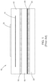
FIG. 2A is a partial side view of a heater having a tuning layer and constructed in accordance with the principles of one form of the present disclosure; -
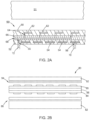
FIG. 2B is an exploded side view of another form of the heater having a tuning layer or tuning heater and constructed in accordance with the principles of the present disclosure; -
FIG. 2C is a perspective exploded view of a heater illustrating an exemplary four (4) zones for the base heater and eighteen (18) zones for the tuning heater in accordance with the principles of the present disclosure; -
FIG. 2D is a side view of another form of a high definition heater system having a supplemental tuning layer and constructed in accordance with the principles of the present disclosure; -
FIG. 3 is a schematic view illustrating a thermal system according to the principles of the present disclosure having four nodes; -
FIG. 4 is a schematic view illustrating a thermal system according to the principles of the present disclosure having three nodes; -
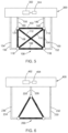
FIG. 5 is a schematic view illustrating the thermal system ofFIG. 2 connected to a control system in accordance with the principles of the present disclosure; -
FIG. 6 is a schematic view illustrating the thermal system ofFIG. 3 connected to a control system in accordance with the principles of the present disclosure; -
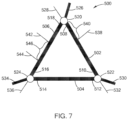
FIG. 7 is a schematic view illustrating a thermal system having three nodes and auxiliary sensing wires for sensing a temperature in one or more zones of interest in accordance with the principles of the present disclosure; and -
FIG. 8 is a flowchart illustrating a method of controlling a thermal array -
FIG. 9 is a schematic view illustrating a control system for controlling the thermal systems ofFIGS. 3, 4 , and7 in accordance with the principles of the present disclosure. - The drawings described herein are for illustration purposes only and are not intended to limit the scope of the present disclosure in any way.
- The following description is merely exemplary in nature and is not intended to limit the present disclosure, application, or uses. For example, the following forms of the present disclosure are directed to chucks for use in semiconductor processing, and in some instances, electrostatic chucks. However, it should be understood that the heaters and systems provided herein may be employed in a variety of applications and are not limited to semiconductor processing applications. It should be understood that throughout the drawings, corresponding reference numerals indicate like or corresponding parts and features.
- Referring to
FIG. 2A , one form of the present disclosure is aheater 50 that includes abase heater layer 52 having at least oneheater circuit 54 embedded therein. Thebase heater layer 52 has at least one aperture 56 (or via) formed there through for connecting theheater circuit 54 to a power supply (not shown) Thebase heater layer 52 provides primary heating while atuning heater layer 60 disposed proximate to theheater layer 52 as shown provides for fine tuning of a heat distribution provided by theheater 50. Thetuning layer 60 includes a plurality ofindividual heating elements 62 embedded therein, which are independently controlled. At least oneaperture 64 is formed through thetuning layer 60 for connecting the plurality ofindividual heating elements 62 to the power supply and controller (not shown). As further shown, arouting layer 66 is disposed between thebase heater layer 52 and thetuning layer 60 and defines aninternal cavity 68. A first set ofelectrical leads 70 connects theheater circuit 54 to the power supply, which extends through theheater layer aperture 56. A second set ofelectrical leads 72 connects a plurality ofheating elements 62 to the power supply and extend through theinternal cavity 68 of therouting layer 66, in addition to theaperture 55 in thebase heater layer 52. It should be understood that therouting layer 66 is optional, and theheater 50 could be employed without therouting layer 66 and instead having only thebase heater layer 52 and thetuning heater layer 60. - In another form, rather than providing fine tuning of a heat distribution, the
tuning layer 60 may alternately be used to measure temperature in thechuck 12. This form provides for a plurality of area-specific or discreet locations, of temperature dependent resistance circuits. Each of these temperature sensors can be individually read via a multiplexing switching arrangement to allow substantially more sensors to be used relative to the number of signal wires required to measure each individual sensor, such as shown in U.S. Patent Application NoUS 13/598,956 substrate 26 to thechuck 12. This same feedback can also be used to replace or augment temperature sensors installed near thebase heater 50 for temperature control ofbase heating zones 54 or balancing plate cooling fluid temperature (not shown) via ancillary cool fluid heat exchangers. - In one form, the
base heater layer 52 and thetuning heater layer 60 are formed from enclosingheater circuit 54 and tuninglayer heating elements 62 in a polyimide material for medium temperature applications, which are generally below 250° C. Further, the polyimide material may be doped with materials in order to increase thermal conductivity. - In other forms, the
base heater layer 52 and/or thetuning heater layer 60 are formed by a layered process, wherein the layer is formed through application or accumulation of a material to a substrate or another layer using processes associated with thick film, thin film, thermal spraying, or sol-gel, among others. - In one form, the
base heating circuit 54 is formed from Inconel® and the tuninglayer heating elements 62 are a Nickel material. In still another form, the tuninglayer heating elements 62 are formed of a material having sufficient temperature coefficient of resistance such that the elements function as both heaters and temperature sensors, commonly referred to as "two-wire control." Such heaters and their materials are disclosed inU.S. Pat. Nos. 7,196,295 and8,378,266 . - With the two-wire control, various forms of the present disclosure include temperature, power, and/or thermal impedance based control over the
layer heating elements 62 through knowledge or measurement of voltage and/or current applied to each of the individual elements in the thermalimpedance tuning layer 60, converted to electrical power and resistance through multiplication and division, corresponding in the first instance, identically to the heat flux output from each of these elements and in the second, a known relationship to the element temperature Together these can be used to calculate and monitor the thermal impedance load on each element to allow an operator or control system to detect and compensate for area-specific thermal changes that may result from, but are not limited to, physical changes in the chamber or chuck due to use or maintenance, processing errors, and equipment degradation. Alternatively, each of the individually controlled heating elements in the thermalimpedance tuning layer 60 can be assigned a setpoint resistance corresponding to the same or different specific temperatures which then modify or gate the heat flux originating from corresponding areas on a substrate through to thebase heater layer 52 to control the substrate temperature during semiconductor processing - In one form, the
base heater 50 is bonded to achuck 51, for example, by using a silicone adhesive or even a pressure sensitive adhesive. Therefore, theheater layer 52 provides primary heating, and thetuning layer 60 fine tunes, or adjusts, the heating profile such that a uniform or desired temperature profile is provided to thechuck 51, and thus the substrate (not shown). - In another form of the present disclosure, the coefficient of thermal expansion (CTE) of the tuning
layer heating elements 62 is matched to the CTE of the tuningheating layer substrate 60 in order to improve thermal sensitivity of the tuninglayer heating elements 62 when exposed to strain loads. Many suitable materials for two-wire control exhibit similar characteristics to Resistor Temperature Devices (RTDs), including resistance sensitivity to both temperature and strain. Matching the CTE of the tuninglayer heating elements 62 to the tuningheater layer substrate 60 reduces strain on the actual heating element. And as the operating temperatures increase, strain levels tend to increase, and thus CTE matching becomes more of a factor. In one form, the tuninglayer heating elements 62 are a high purity Nickel-Iron alloy having a CTE of approximately 15 ppm/° C., and the polyimide material that encloses it has a CTE of approximately 16 ppm/° C. In this form, materials that bond the tuningheater layer 60 to the other layers exhibit elastic characteristics that physically decouple thetuning heater layer 60 from other members of thechuck 12. It should be understood that other materials with comparable CTEs may also be employed while remaining within the scope of the present disclosure. - Referring now to
FIGS. 2B-2D , one exemplary form of the heater having both a base heater layer and a tuning layer (as generally set forth above inFIG. 2A ) is illustrated and generally indicated byreference numeral 80. Theheater 80 includes a base plate ortarget 82, (also referred to as a cooling plate), which in one form is an Aluminum plate approximately 16 mm in thickness. Abase heater 84 is secured to the base plate ortarget 82, in one form using anelastomeric bond layer 86 as shown. The elastomeric bond may be one disclosed inU.S. Pat. No. 6,073,577 . Asubstrate 88 is disposed on top of thebase heater 84 and is an Aluminum material approximately 1 mm in thickness according to one form of the present disclosure. Thesubstrate 88 is designed to have a thermal conductivity to dissipate a requisite amount of power from thebase heater 84. Because thebase heater 84 has relatively high power, without a requisite amount of thermal conductivity, thisbase heater 84 would leave "witness" marks (from the resistive circuit trace) on adjacent components, thereby reducing the performance of the overall heater system. - A tuning
heater 90 is disposed on top of thesubstrate 88 and is secured to achuck 92 using anelastomeric bond layer 94, as set forth above. Thechuck 92 in one form is an Aluminum Oxide material having a thickness of approximately 2.5 mm. It should be understood that the materials and dimensions as set forth herein are merely exemplary and thus the present disclosure is not limited to the specific forms as set forth herein. Additionally, the tuningheater 90 has lower power than thebase heater 84, and as set forth above, thesubstrate 88 functions to dissipate power from thebase heater 84 such that "witness" marks do not form on the tuningheater 90. - The
base heater 84 and the tuningheater 90 are shown in greater detail inFIG. 2C in which an exemplary four (4) zones are shown for thebase heater 84, and eighteen (18) zones for the tuningheater 90. In one form, theheater 80 is adapted for use with chuck sizes of 450 mm, however, theheater 80 may be employed with larger or smaller chuck sizes due to its ability to highly tailor the heat distribution. Additionally, thehigh definition heater 80 may be employed around a periphery of thechuck 92, or in predetermined locations across thechuck 92, rather than in a stacked/planar configuration as illustrated herein. Further still, thehigh definition heater 80 may be employed in process kits, chamber walls, lids, gas lines, and showerheads, among other components within semiconductor processing equipment. It should also be understood that the heaters and control systems illustrated and described herein may be employed in any number of applications, and thus the exemplary semiconductor heater chuck application should not be construed as limiting the scope of the present disclosure. - The present disclosure also contemplates that the
base heater 84 and the tuningheater 90 not be limited to a heating function. It should be understood that one or more of these members, referred to as a "base functional layer" and a "tuning layer," respectively, may alternately be a temperature sensor layer or other functional member while remaining within the scope of the present disclosure. - As shown in
FIG. 2D a dual tuning capability may be provided with the inclusion of a secondarytuning layer heater 99 on the top surface of thechuck 92. The secondary tuning layer may alternately be used as a temperature sensing layer rather than a heating layer while remaining within the scope of the present disclosure. Accordingly, any number of tuning layer heaters may be employed and should not be limited to those illustrated and described herein. It should also be understood that the thermal array as set forth in the following may be employed with a single heater or multiple heaters, whether layered or in other configurations, while remaining within the scope of the present disclosure. - Referring to
FIG. 3 , athermal system 100 for use in a thermal array system, such as those described inFIGS. 2A-2D is shown. Thethermal system 100 includes sixresistor circuits thermal system 100 includes fournodes resistor circuits - Each of the six
resistor circuits resistor circuits resistor circuit 102 has termination ends 122 and 124.Resistor circuit 104 has termination ends 126 and 128.Resistor circuit 106 has termination ends 130 and 132.Resistor circuit 108 has termination ends 134 and 136.Resistor circuit 110 has termination ends 138 and 140. Finally,resistor circuit 112 as termination ends 142 and 144. - In this example,
termination end 124 ofresistor circuit 102,termination end 138 ofresistor circuit 110, andtermination end 126 ofresistor circuit 104 are connected tonode 114.Termination end 122 ofresistor circuit 102,termination end 144 ofresistor circuit 112, andtermination end 136 ofresistor circuit 108 are connected tonode 120.Termination end 132 ofresistor circuit 106,termination end 140 ofresistor circuit 110, andtermination end 134 ofresistor circuit 108 are connected tonode 118. Finally,termination end 142 ofresistor circuit 112,termination end 128 ofresistor circuit 104, andtermination end 130 ofresistor circuit 106 are connected tonode 116. - Each of the
nodes resistor circuits circuits - Here,
node 114 has apower wire 146 and asignal wire 148 protruding therefrom.Node 116 has apower wire 150 and asignal wire 152 protruding therefrom.Node 118 has apower wire 154 and asignal wire 156 protruding therefrom. Finally,node 120 has apower wire 158 and asignal wire 160 protruding therefrom. All of these wires may be connected to a control system which will be described later in this description. - By selectively providing either a power or ground signal to the
power wires resistor circuits resistor circuits - The table below illustrates each combination of power or ground signal provided to the
power wires nodes Node 120Node 118Node 116Node 114Heating Circuits GND GND GND GND None GND GND GND PWR 102, 104, 110 GND GND PWR GND 104, 106, 112 GND GND PWR PWR 102, 106, 110, 112 GND PWR GND GND 106, 108, 110 GND PWR GND PWR 102, 104, 106, 108 GND PWR PWR GND 104, 108, 110, 112 GND PWR PWR PWR 102, 108, 112 PWR GND GND GND 102, 108, 112 PWR GND GND PWR 104, 108, 110, 112 PWR GND PWR GND 102, 104, 106, 108 PWR GND PWR PWR 106, 108, 110 PWR PWR GND GND 102, 106, 110, 112 PWR PWR GND PWR 104, 106, 112 PWR PWR PWR GND 102, 104, 110 PWR PWR PWR PWR None - Referring to
FIG. 4 , another example of thethermal system 200 is shown.Thermal system 200 includesresistor circuits resistor circuit 202 has termination ends 208 and 210,resistor circuit 204 has termination ends 212 and 214, whileresistor circuit 206 has termination ends 216 and 218. - The
system 200 includesnodes node 220 are termination ends 208 and 218 ofresistor circuits resistor circuits node 224 are termination ends 214 and 216 ofresistor circuits FIG. 3 , each of thenodes node 220 has apower wire 226 and asignal wire 228 protruding therefrom. Node 222 has apower wire 230 and asignal wire 232 protruding therefrom. Finally,node 224 has apower wire 234 and asignal wire 236 protruding therefrom. - As such, a control system can provide a power or ground signal to each of the
power wires resistor circuits nodes signal wires resistor circuits resistor circuits - The table below illustrates each combination of power or ground signal provided to the
power wires nodes Node 224Node 222 Node 220Heating Circuits GND GND GND None GND GND PWR 202, 206 GND PWR GND 202, 204 GND PWR PWR 204, 206 PWR GND GND 204, 206 PWR GND PWR 202, 204 PWR PWR GND 202, 206 PWR PWR PWR None - It should be understood that any one of a number of different combinations of nodes and resistor circuits could be utilized. As stated before, the examples given in
FIGS. 3 and 4 are just two types of examples and there can be any one of a number of different configurations that involve any one of a number of different nodes and/or resistor circuits - Generally, the plurality of resistor circuits defines a number of resistor circuits Rn. The plurality of nodes defining a number of nodes Nn. The plurality of power wires are connected to each of the plurality of nodes to provide power to the plurality of resistor circuits, wherein the plurality of power wires defining a number of power wires Pn. A plurality of signal wires connects to each of the plurality of nodes to sense the temperature of each of the plurality of resistor circuits. The plurality of signal wires defining a number of signal wires Sn. The number of power wires Pn and the number of signal wires Sn is equal to the number of nodes Nn, and the number of resistor circuits Rn is greater than or equal to the number of nodes Nn.
- Referring to
FIG. 5 , thethermal system 100 ofFIG. 3 is shown coupled to acontrol system 300. More specifically, thecontrol system 300 has aprocessor 302 that is in communication with amemory 304. Thememory 304 may contain instructions that configure theprocessor 302 to perform any one of a number of different functions. - These functions may include providing power to the
power wires thermal system 100 or taking measurements of thesignal wires - In this example, the
power wires signal wires control system 300 and therefore are in communication with theprocessor 302 of thecontrol system 300 for receiving power or measuring signals. Of course, it should be understood that the instructions configuring theprocessor 302 may be stored within the processor or at a remote storage location and not necessarily thememory 304. - Referring to
FIG. 6 , thethermal system 200 ofFIG. 4 is shown connected to acontrol system 400. Like thecontrol system 300, thecontrol system 400 includes aprocessor 402 as well as amemory 404 in communication with theprocessor 402. Thememory 404 may contain instructions for configuring the processor to perform any one of a number of different functions including providing power to the power wires to 226, 230, and 234 of thethermal system 200. Additionally, the instructions may configure the processor to perform measurements across thesignal wires thermal system 200. Of course, it should be understood that the instructions configuring theprocessor 402 may be stored within the processor or at a remote storage location and not necessarily thememory 404. - Referring to
FIG. 7 , another example of thethermal system 500 is shown. Here, thethermal system 500 is similar to thethermal system 200 ofFIG. 4 . However,thermal system 500 includes additional auxiliary signal wires that will be described in the paragraphs that follow. Like athermal system 200,thermal system 500 includesresistor circuits resistor circuit 502 has termination ends 508 and 510,resistor circuit 504 has termination ends 512 and 514, whileresistor circuit 506 has termination ends 516 and 518. - The
system 500 includesnodes node 520 are termination ends 508 and 518 ofresistor circuits node 522 are termination ends 510 and 512 ofresistor circuits node 524 are termination ends 514 and 516 ofresistor circuits FIG. 4 , each of thenodes node 520 has apower wire 526 and asignal wire 528 protruding therefrom.Node 522 has apower wire 530 and asignal wire 532 protruding therefrom. Finally,node 524 has apower wire 534 and asignal wire 536 protruding therefrom. - As such, a control system can provide a power or ground signal to each of the
power wires system 200. Similarly, the control system could measure the resistance between any of theresistor circuits nodes signal wires resistor circuits resistor circuits - However,
system 500 may also include anauxiliary signal wire 538 connected toresistor circuit 502. Theauxiliary signal wire 538 can be connected to the control system described in this specification and would allow for measurements of resistance, and therefore temperature, in a zone ofinterest 540. Additionally, or alternatively, one or more auxiliary signal wires may be connected to any of the resistor circuits so as to monitor the temperature in any one of a number of different zones of interest. For example,system 500 may also includeauxiliary signal wires resistor circuit 506. Theseauxiliary signal wires interest 546, which is between thenodes - As such, any one of a number of different auxiliary wires may be connected to the resistor circuits to allow monitoring of the temperature of multiple zones of interest. Further, the use of one or more auxiliary wires may be used in any example described herein, such as the example shown in
FIG. 3 . - Now referring to
FIG. 8 , amethod 600 is provided for controlling the thermal system. Themethod 600 can be utilized controlling any of the thermal array systems described and can be executed by any of the control systems described The method starts atblock 610. Inblock 612 the controller calculates the set points for each resistor circuit of the array. For example, resistance set points may be set for each resistor circuit such that a measured resistance for that resistor circuit can be used as a trigger to stop providing power to that resistor circuit. Inblock 614, the time window for each resistor circuit is calculated. The time window may be the time allotted to power a particular resistor circuit. Although, if the resistor circuit resistance is above the set point, the controller may remain dormant for the remainder of the time window or may directly move to the next window to power the next resistor circuit. However, it may be desirable to have a minimum wait time for each resistor circuit such that power is not constantly provided to the system for measurement purposes, thereby heating elements beyond what is necessary for the heating application. - In
block 616, the controller determines if the end of the time window has been reached for the current resistor circuit. If the end of the time window had been reached for the current resistor circuit, the method followsline 620 to block 622. Inblock 622, the controller increments to the next resistor circuit within the array and proceeds to block 616 where the process continues. If the end of the time window has not been reached the method followsline 618 to block 624. Inblock 624, the controller may simultaneously provide power to the resistor circuit and measure electrical characteristics of the resistor circuit. Inblock 626, the controller determines if the resistor circuit has exceeded the resistor circuit set point based on the measured characteristics. If the set point has been exceeded, the method may wait until the timing window is complete or, after some delay, proceed along theline 628 to block 622. Inblock 622, the resistor circuit is incremented to the next resistor circuit and the process proceeds to block 616. If the resistor circuit has not exceeded the set point based on the measured characteristics, the process followsline 630 to block 616 where the process continues. - Any of the controllers, control systems, or engines described may be implemented in one or more computer systems. One exemplary system is provided in
FIG. 9 . Thecomputer system 700 includes aprocessor 710 for executing instructions such as those described in the methods discussed above. The instructions may be stored in a computer readable medium such asmemory 712 orstorage devices 714, for example a disk drive, CD, or DVD. The computer may include adisplay controller 716 responsive to instructions to generate a textual or graphical display on adisplay device 718, for example a computer monitor. In addition, theprocessor 710 may communicate with anetwork controller 720 to communicate data or instructions to other systems, for example other general computer systems. Thenetwork controller 720 may communicate over Ethernet or other known protocols to distribute processing or provide remote access to information over a variety of network topologies, including local area networks, wide area networks, the Internet, or other commonly used network topologies. - As a person skilled in the art will readily appreciate, the above description is meant as an illustration of implementation of the principles this invention. This description is not intended to limit the scope or application of this invention in that the invention is susceptible to modification, variation and change, without departing from the invention, as defined in the following claims.
Claims (13)
- A system comprising a control system (300, 400, 500) coupled to a thermal system (100), the thermal system (100) comprising a heater, a plurality of nodes (114, 116, 118, 120), a plurality of power wires (146, 150, 154, 158), and a plurality of signal wires (148, 152, 156, 160), whereby:the heater comprises a plurality of heating resistor circuits (102, 104, 106, 108, 110, 112), each of the heating resistor circuits (102, 104, 106, 108, 110, 112) having a first termination end and a second termination end (122, 124, 126, 128, 130, 132, 134, 136, 138, 140, 142), the plurality of heating resistor circuits (102, 104, 106, 108, 110, 112) defining a number of heating resistor circuits Rn;the plurality of nodes (114, 116, 118, 120) connect the plurality of heating resistor circuits (102, 104, 106, 108, 110, 112) at each of the first and second termination ends (122, 124, 126, 128, 130, 132, 134, 136, 138, 140, 142), the plurality of nodes (114, 116, 118, 120) defining a number of nodes Nn;the plurality of power wires (146, 150, 154, 158) connected to each of the plurality of nodes (114, 116, 118, 120) to provide power to the plurality of heating resistor circuits (102, 104, 106, 108, 110, 112), the plurality of power wires (146, 150, 154, 158) defining a number of power wires Pn;the plurality of signal wires (148, 152, 156, 160) connected to each of the plurality of nodes (114, 116, 118, 120) to sense a temperature of each of the plurality of heating resistor circuits (102, 104, 106, 108, 110, 112), the plurality of signal wires (148, 152, 156, 160) defining a number of signal wires Sn;wherein the number of power wires Pn and the number of signal wires Sn is equal to the number of nodes Nn, and the number of heating resistor circuits Rn is greater than or equal to the number of nodes Nn;wherein each of the plurality of nodes (114, 116, 118, 120) is connected to one power wire from among the plurality of power wires (146, 150, 154, 158) and one signal wire from among the plurality of signal wires (148, 152, 156, 160), said power wire being different from said signal wire;characterized in that the control system (300, 400, 500) is connected to the plurality of signal wires (148, 152, 156, 160) and the plurality of power wires (146, 150, 154, 158), and the control system (300, 400, 500) is connected to the plurality of nodes (114, 116, 118, 120) via the plurality of signal wires (148, 152, 156, 160) and the plurality of power wires (146, 150, 154, 158), andin that the control system (300, 400, 500) provides a power signal or a ground signal to the power wires, and the control system (300, 400, 500) measures a resistance of each of the heating resistor circuits (102, 104, 106, 108, 110, 112) using the plurality of signal wires (148, 152, 156, 160) and calculates temperature of each of the heating resistor circuits (102, 104, 106, 108, 110, 112) using the resistance.
- The system of claim 1, wherein the plurality of heating resistor circuits (102, 104, 106, 108, 110, 112) each comprise a resistive heating element.
- The system of claim 2, wherein the resistive heating element is selected from the group consisting of a layered heating element, an etched foil element, or a wire wound element.
- The system of claim 1, wherein the signal wires (148, 152, 156, 160) comprise a platinum material.
- The system of claim 1, wherein the number of heating resistor circuits Rn is six, and the number of power wires Pn, signal wires Sn, and nodes Nn is four.
- The system of claim 1, wherein the number of heating resistor circuits Rn is three, and the number of power wires Pn, signal wires Sn, and nodes Nn is three.
- The system of claim 1, further comprising a sensing element connected to the signal wires (148, 152, 156, 160).
- The system of claim 7, wherein the sensing element is a thermocouple.
- The system of claim 7, wherein the sensing element is a resistance temperature detector.
- The system of claim 1, further comprising a first auxiliary signal wire (538) connected to the heating resistor circuit at a location between the first and second termination ends (122, 124, 126, 128, 130, 132, 134, 136, 138, 140, 142) of the heating resistor circuit to sense the temperature of a portion of the heating resistor circuit between the first auxiliary signal wire and the signal wires (148, 152, 156, 160).
- The system of claim 10, further comprising a second auxiliary signal wire (542) connected to the heating resistor circuit at a second location between the first and second termination ends (122, 124, 126, 128, 130, 132, 134, 136, 138, 140, 142) of the heating resistor circuit to sense the temperature of a portion of the heating resistor circuit between the first auxiliary signal wire (538) and the second auxiliary signal wire (542).
- A method of controlling temperature of a heater comprising employing the system according to claim 1.
- A heater system comprising:a heating target (82); anda system according to any one of claims 1 to 11, the heater of the system being secured to the heating target.
Applications Claiming Priority (2)
| Application Number | Priority Date | Filing Date | Title |
|---|---|---|---|
| US14/925,330 US9826574B2 (en) | 2015-10-28 | 2015-10-28 | Integrated heater and sensor system |
| PCT/US2016/058382 WO2017074838A1 (en) | 2015-10-28 | 2016-10-24 | Integrated heater and sensor system |
Publications (2)
| Publication Number | Publication Date |
|---|---|
| EP3351054A1 EP3351054A1 (en) | 2018-07-25 |
| EP3351054B1 true EP3351054B1 (en) | 2024-01-17 |
Family
ID=57288489
Family Applications (1)
| Application Number | Title | Priority Date | Filing Date |
|---|---|---|---|
| EP16795181.3A Active EP3351054B1 (en) | 2015-10-28 | 2016-10-24 | Integrated heater and sensor system |
Country Status (7)
| Country | Link |
|---|---|
| US (2) | US9826574B2 (en) |
| EP (1) | EP3351054B1 (en) |
| JP (2) | JP6543769B2 (en) |
| KR (2) | KR102011645B1 (en) |
| CN (2) | CN111132391B (en) |
| TW (1) | TWI613748B (en) |
| WO (1) | WO2017074838A1 (en) |
Families Citing this family (10)
| Publication number | Priority date | Publication date | Assignee | Title |
|---|---|---|---|---|
| US10582570B2 (en) * | 2016-01-22 | 2020-03-03 | Applied Materials, Inc. | Sensor system for multi-zone electrostatic chuck |
| US11508600B2 (en) * | 2017-04-10 | 2022-11-22 | Ngk Spark Plug Co., Ltd. | Holding device |
| CN115468626B (en) * | 2017-07-27 | 2025-11-04 | 沃特洛电气制造公司 | Sensor systems and integrated heater-sensor systems for measuring and controlling the performance of heater systems. |
| JP7349439B2 (en) * | 2017-11-21 | 2023-09-22 | ワトロー エレクトリック マニュファクチュアリング カンパニー | Multi-zone pedestal heater with channel layer |
| KR102235765B1 (en) * | 2018-08-24 | 2021-04-01 | 어플라이드 머티어리얼스, 인코포레이티드 | Electrostatic Chuck and manufacturing process for Electrostatic Chuck |
| US11831226B2 (en) * | 2019-01-10 | 2023-11-28 | Vestas Wind Systems A/S | Cooling of electrical generators in wind turbines |
| US12452962B2 (en) | 2020-03-25 | 2025-10-21 | Lockheed Martin Corporation | Robust versatile monolithic resistive system for tailored heating |
| US12140752B2 (en) | 2020-12-29 | 2024-11-12 | Beijing Voyager Technology Co., Ltd. | Thermal control of MEMS mirrors to limit resonant frequency shift |
| CN120035788B (en) * | 2023-03-03 | 2026-02-06 | 京东方科技集团股份有限公司 | Array substrate and liquid crystal display panel |
| WO2025169030A1 (en) * | 2024-02-05 | 2025-08-14 | Corintis Sa | Thermal device |
Family Cites Families (29)
| Publication number | Priority date | Publication date | Assignee | Title |
|---|---|---|---|---|
| EP0543181B1 (en) * | 1991-11-18 | 1998-03-25 | MICAFIL Vakuumtechnik AG | Method of drying the solid insulating material of transformers, especially transformers for distribution installations, and apparatus therefor |
| US5948298A (en) * | 1996-04-26 | 1999-09-07 | Ford Global Technologies, Inc. | Battery heating system |
| US5802856A (en) * | 1996-07-31 | 1998-09-08 | Stanford University | Multizone bake/chill thermal cycling module |
| US6080971A (en) * | 1997-05-22 | 2000-06-27 | David Seitz | Fluid heater with improved heating elements controller |
| US6415858B1 (en) * | 1997-12-31 | 2002-07-09 | Temptronic Corporation | Temperature control system for a workpiece chuck |
| US6073577A (en) | 1998-06-30 | 2000-06-13 | Lam Research Corporation | Electrode for plasma processes and method for manufacture and use thereof |
| US6139627A (en) * | 1998-09-21 | 2000-10-31 | The University Of Akron | Transparent multi-zone crystal growth furnace and method for controlling the same |
| US6353209B1 (en) * | 1999-03-04 | 2002-03-05 | Board Of Trustees Of The Leland Stanford Junior University | Temperature processing module |
| US6617553B2 (en) * | 1999-05-19 | 2003-09-09 | Applied Materials, Inc. | Multi-zone resistive heater |
| US6259072B1 (en) * | 1999-11-09 | 2001-07-10 | Axcelis Technologies, Inc. | Zone controlled radiant heating system utilizing focused reflector |
| US6852287B2 (en) * | 2001-09-12 | 2005-02-08 | Handylab, Inc. | Microfluidic devices having a reduced number of input and output connections |
| US7196295B2 (en) | 2003-11-21 | 2007-03-27 | Watlow Electric Manufacturing Company | Two-wire layered heater system |
| JP4528150B2 (en) * | 2005-02-14 | 2010-08-18 | 京セラ株式会社 | Concavity and convexity pattern detection apparatus and method |
| KR100925033B1 (en) * | 2005-06-29 | 2009-11-04 | 와틀로 일렉트릭 매뉴팩츄어링 컴파니 | Smart layered heater surfaces |
| KR100690926B1 (en) | 2006-02-03 | 2007-03-09 | 삼성전자주식회사 | Micro Heat Flux Sensor Array |
| JPWO2007091299A1 (en) * | 2006-02-07 | 2009-06-25 | 株式会社島津製作所 | TFT substrate heating method, TFT substrate temperature measurement method, and TFT substrate temperature control method |
| CA2877959C (en) * | 2006-08-22 | 2017-06-13 | Charles F. Barry | Apparatus and method for thermal stabilization of pcb-mounted electronic components within an enclosed housing |
| US8373266B2 (en) * | 2007-03-29 | 2013-02-12 | Continental Automotive Systems, Inc. | Heat sink mounted on a vehicle-transmission case |
| US20080302783A1 (en) * | 2007-06-08 | 2008-12-11 | Anthony Yeh Chiing Wong | Actively controlled embedded burn-in board thermal heaters |
| FR2926675B1 (en) * | 2008-01-18 | 2011-07-29 | Univ Paris Sud | METHOD OF OBTAINING A MATERIAL STRUCTURED WITH CROSSING OPENINGS, PARTICULARLY OF TYPE III SEMICONDUCTOR NITRIDE STRUCTURES ACCORDING TO PHOTONIC CRYSTAL PATTERNS |
| JP2010153730A (en) | 2008-12-26 | 2010-07-08 | Omron Corp | Wiring structure, heater driving device, measuring device, and control system |
| US8637794B2 (en) * | 2009-10-21 | 2014-01-28 | Lam Research Corporation | Heating plate with planar heating zones for semiconductor processing |
| JP5424048B2 (en) * | 2010-03-24 | 2014-02-26 | 理化工業株式会社 | Multi-channel power controller |
| US20130047918A1 (en) * | 2011-08-22 | 2013-02-28 | Soitec | Deposition systems including a precursor gas furnace within a reaction chamber, and related methods |
| KR101813635B1 (en) * | 2011-08-30 | 2017-12-29 | 와틀로 일렉트릭 매뉴팩츄어링 컴파니 | System and method for controlling a thermal array |
| US8461674B2 (en) * | 2011-09-21 | 2013-06-11 | Lam Research Corporation | Thermal plate with planar thermal zones for semiconductor processing |
| EP2820915B1 (en) | 2012-02-27 | 2017-01-04 | Watlow Electric Manufacturing Company | Temperature detection and control system for layered heaters |
| KR101373610B1 (en) * | 2013-01-03 | 2014-03-14 | 박대규 | Smart grill and temperature control method thereof |
| JP6100672B2 (en) * | 2013-10-25 | 2017-03-22 | 東京エレクトロン株式会社 | Temperature control mechanism, temperature control method, and substrate processing apparatus |
-
2015
- 2015-10-28 US US14/925,330 patent/US9826574B2/en active Active
-
2016
- 2016-10-24 WO PCT/US2016/058382 patent/WO2017074838A1/en not_active Ceased
- 2016-10-24 EP EP16795181.3A patent/EP3351054B1/en active Active
- 2016-10-24 CN CN201911231839.5A patent/CN111132391B/en not_active Expired - Fee Related
- 2016-10-24 KR KR1020187013860A patent/KR102011645B1/en active Active
- 2016-10-24 CN CN201680063548.8A patent/CN108432341B/en not_active Expired - Fee Related
- 2016-10-24 KR KR1020197023358A patent/KR102110268B1/en active Active
- 2016-10-24 JP JP2018521379A patent/JP6543769B2/en active Active
- 2016-10-27 TW TW105134782A patent/TWI613748B/en active
-
2017
- 2017-11-20 US US15/817,573 patent/US10362637B2/en active Active
-
2019
- 2019-06-17 JP JP2019111830A patent/JP6905549B2/en active Active
Also Published As
| Publication number | Publication date |
|---|---|
| US9826574B2 (en) | 2017-11-21 |
| WO2017074838A1 (en) | 2017-05-04 |
| US20180077752A1 (en) | 2018-03-15 |
| KR20190096443A (en) | 2019-08-19 |
| CN111132391A (en) | 2020-05-08 |
| US20170127474A1 (en) | 2017-05-04 |
| KR20180059558A (en) | 2018-06-04 |
| US10362637B2 (en) | 2019-07-23 |
| TW201721792A (en) | 2017-06-16 |
| CN108432341B (en) | 2020-01-03 |
| JP6543769B2 (en) | 2019-07-10 |
| CN108432341A (en) | 2018-08-21 |
| CN111132391B (en) | 2021-11-16 |
| KR102110268B1 (en) | 2020-05-13 |
| KR102011645B1 (en) | 2019-08-19 |
| JP2019208028A (en) | 2019-12-05 |
| EP3351054A1 (en) | 2018-07-25 |
| JP6905549B2 (en) | 2021-07-21 |
| TWI613748B (en) | 2018-02-01 |
| JP2018537811A (en) | 2018-12-20 |
Similar Documents
| Publication | Publication Date | Title |
|---|---|---|
| US10362637B2 (en) | Integrated heater and sensor system | |
| US10340162B2 (en) | Reduced wire count heater array block | |
| US10361103B2 (en) | High definition heater system having a fluid medium |
Legal Events
| Date | Code | Title | Description |
|---|---|---|---|
| STAA | Information on the status of an ep patent application or granted ep patent |
Free format text: STATUS: UNKNOWN |
|
| STAA | Information on the status of an ep patent application or granted ep patent |
Free format text: STATUS: THE INTERNATIONAL PUBLICATION HAS BEEN MADE |
|
| PUAI | Public reference made under article 153(3) epc to a published international application that has entered the european phase |
Free format text: ORIGINAL CODE: 0009012 |
|
| STAA | Information on the status of an ep patent application or granted ep patent |
Free format text: STATUS: REQUEST FOR EXAMINATION WAS MADE |
|
| 17P | Request for examination filed |
Effective date: 20180418 |
|
| AK | Designated contracting states |
Kind code of ref document: A1 Designated state(s): AL AT BE BG CH CY CZ DE DK EE ES FI FR GB GR HR HU IE IS IT LI LT LU LV MC MK MT NL NO PL PT RO RS SE SI SK SM TR |
|
| AX | Request for extension of the european patent |
Extension state: BA ME |
|
| DAV | Request for validation of the european patent (deleted) | ||
| DAX | Request for extension of the european patent (deleted) | ||
| STAA | Information on the status of an ep patent application or granted ep patent |
Free format text: STATUS: EXAMINATION IS IN PROGRESS |
|
| 17Q | First examination report despatched |
Effective date: 20191206 |
|
| GRAP | Despatch of communication of intention to grant a patent |
Free format text: ORIGINAL CODE: EPIDOSNIGR1 |
|
| STAA | Information on the status of an ep patent application or granted ep patent |
Free format text: STATUS: GRANT OF PATENT IS INTENDED |
|
| INTG | Intention to grant announced |
Effective date: 20230310 |
|
| GRAJ | Information related to disapproval of communication of intention to grant by the applicant or resumption of examination proceedings by the epo deleted |
Free format text: ORIGINAL CODE: EPIDOSDIGR1 |
|
| STAA | Information on the status of an ep patent application or granted ep patent |
Free format text: STATUS: EXAMINATION IS IN PROGRESS |
|
| GRAP | Despatch of communication of intention to grant a patent |
Free format text: ORIGINAL CODE: EPIDOSNIGR1 |
|
| STAA | Information on the status of an ep patent application or granted ep patent |
Free format text: STATUS: GRANT OF PATENT IS INTENDED |
|
| INTC | Intention to grant announced (deleted) | ||
| INTG | Intention to grant announced |
Effective date: 20230801 |
|
| GRAJ | Information related to disapproval of communication of intention to grant by the applicant or resumption of examination proceedings by the epo deleted |
Free format text: ORIGINAL CODE: EPIDOSDIGR1 |
|
| STAA | Information on the status of an ep patent application or granted ep patent |
Free format text: STATUS: EXAMINATION IS IN PROGRESS |
|
| GRAP | Despatch of communication of intention to grant a patent |
Free format text: ORIGINAL CODE: EPIDOSNIGR1 |
|
| STAA | Information on the status of an ep patent application or granted ep patent |
Free format text: STATUS: GRANT OF PATENT IS INTENDED |
|
| INTC | Intention to grant announced (deleted) | ||
| GRAS | Grant fee paid |
Free format text: ORIGINAL CODE: EPIDOSNIGR3 |
|
| GRAA | (expected) grant |
Free format text: ORIGINAL CODE: 0009210 |
|
| STAA | Information on the status of an ep patent application or granted ep patent |
Free format text: STATUS: THE PATENT HAS BEEN GRANTED |
|
| INTG | Intention to grant announced |
Effective date: 20231122 |
|
| AK | Designated contracting states |
Kind code of ref document: B1 Designated state(s): AL AT BE BG CH CY CZ DE DK EE ES FI FR GB GR HR HU IE IS IT LI LT LU LV MC MK MT NL NO PL PT RO RS SE SI SK SM TR |
|
| REG | Reference to a national code |
Ref country code: GB Ref legal event code: FG4D |
|
| REG | Reference to a national code |
Ref country code: CH Ref legal event code: EP |
|
| REG | Reference to a national code |
Ref country code: DE Ref legal event code: R096 Ref document number: 602016085381 Country of ref document: DE |
|
| REG | Reference to a national code |
Ref country code: IE Ref legal event code: FG4D |
|
| REG | Reference to a national code |
Ref country code: NL Ref legal event code: FP |
|
| REG | Reference to a national code |
Ref country code: LT Ref legal event code: MG9D |
|
| REG | Reference to a national code |
Ref country code: AT Ref legal event code: MK05 Ref document number: 1651374 Country of ref document: AT Kind code of ref document: T Effective date: 20240117 |
|
| PG25 | Lapsed in a contracting state [announced via postgrant information from national office to epo] |
Ref country code: IS Free format text: LAPSE BECAUSE OF FAILURE TO SUBMIT A TRANSLATION OF THE DESCRIPTION OR TO PAY THE FEE WITHIN THE PRESCRIBED TIME-LIMIT Effective date: 20240517 |
|
| PG25 | Lapsed in a contracting state [announced via postgrant information from national office to epo] |
Ref country code: LT Free format text: LAPSE BECAUSE OF FAILURE TO SUBMIT A TRANSLATION OF THE DESCRIPTION OR TO PAY THE FEE WITHIN THE PRESCRIBED TIME-LIMIT Effective date: 20240117 |
|
| PG25 | Lapsed in a contracting state [announced via postgrant information from national office to epo] |
Ref country code: GR Free format text: LAPSE BECAUSE OF FAILURE TO SUBMIT A TRANSLATION OF THE DESCRIPTION OR TO PAY THE FEE WITHIN THE PRESCRIBED TIME-LIMIT Effective date: 20240418 |
|
| PG25 | Lapsed in a contracting state [announced via postgrant information from national office to epo] |
Ref country code: HR Free format text: LAPSE BECAUSE OF FAILURE TO SUBMIT A TRANSLATION OF THE DESCRIPTION OR TO PAY THE FEE WITHIN THE PRESCRIBED TIME-LIMIT Effective date: 20240117 Ref country code: RS Free format text: LAPSE BECAUSE OF FAILURE TO SUBMIT A TRANSLATION OF THE DESCRIPTION OR TO PAY THE FEE WITHIN THE PRESCRIBED TIME-LIMIT Effective date: 20240417 |
|
| PG25 | Lapsed in a contracting state [announced via postgrant information from national office to epo] |
Ref country code: ES Free format text: LAPSE BECAUSE OF FAILURE TO SUBMIT A TRANSLATION OF THE DESCRIPTION OR TO PAY THE FEE WITHIN THE PRESCRIBED TIME-LIMIT Effective date: 20240117 |
|
| PG25 | Lapsed in a contracting state [announced via postgrant information from national office to epo] |
Ref country code: AT Free format text: LAPSE BECAUSE OF FAILURE TO SUBMIT A TRANSLATION OF THE DESCRIPTION OR TO PAY THE FEE WITHIN THE PRESCRIBED TIME-LIMIT Effective date: 20240117 |
|
| PG25 | Lapsed in a contracting state [announced via postgrant information from national office to epo] |
Ref country code: RS Free format text: LAPSE BECAUSE OF FAILURE TO SUBMIT A TRANSLATION OF THE DESCRIPTION OR TO PAY THE FEE WITHIN THE PRESCRIBED TIME-LIMIT Effective date: 20240417 Ref country code: NO Free format text: LAPSE BECAUSE OF FAILURE TO SUBMIT A TRANSLATION OF THE DESCRIPTION OR TO PAY THE FEE WITHIN THE PRESCRIBED TIME-LIMIT Effective date: 20240417 Ref country code: LT Free format text: LAPSE BECAUSE OF FAILURE TO SUBMIT A TRANSLATION OF THE DESCRIPTION OR TO PAY THE FEE WITHIN THE PRESCRIBED TIME-LIMIT Effective date: 20240117 Ref country code: IS Free format text: LAPSE BECAUSE OF FAILURE TO SUBMIT A TRANSLATION OF THE DESCRIPTION OR TO PAY THE FEE WITHIN THE PRESCRIBED TIME-LIMIT Effective date: 20240517 Ref country code: HR Free format text: LAPSE BECAUSE OF FAILURE TO SUBMIT A TRANSLATION OF THE DESCRIPTION OR TO PAY THE FEE WITHIN THE PRESCRIBED TIME-LIMIT Effective date: 20240117 Ref country code: GR Free format text: LAPSE BECAUSE OF FAILURE TO SUBMIT A TRANSLATION OF THE DESCRIPTION OR TO PAY THE FEE WITHIN THE PRESCRIBED TIME-LIMIT Effective date: 20240418 Ref country code: FI Free format text: LAPSE BECAUSE OF FAILURE TO SUBMIT A TRANSLATION OF THE DESCRIPTION OR TO PAY THE FEE WITHIN THE PRESCRIBED TIME-LIMIT Effective date: 20240117 Ref country code: ES Free format text: LAPSE BECAUSE OF FAILURE TO SUBMIT A TRANSLATION OF THE DESCRIPTION OR TO PAY THE FEE WITHIN THE PRESCRIBED TIME-LIMIT Effective date: 20240117 Ref country code: BG Free format text: LAPSE BECAUSE OF FAILURE TO SUBMIT A TRANSLATION OF THE DESCRIPTION OR TO PAY THE FEE WITHIN THE PRESCRIBED TIME-LIMIT Effective date: 20240117 Ref country code: AT Free format text: LAPSE BECAUSE OF FAILURE TO SUBMIT A TRANSLATION OF THE DESCRIPTION OR TO PAY THE FEE WITHIN THE PRESCRIBED TIME-LIMIT Effective date: 20240117 |
|
| PG25 | Lapsed in a contracting state [announced via postgrant information from national office to epo] |
Ref country code: PL Free format text: LAPSE BECAUSE OF FAILURE TO SUBMIT A TRANSLATION OF THE DESCRIPTION OR TO PAY THE FEE WITHIN THE PRESCRIBED TIME-LIMIT Effective date: 20240117 Ref country code: PT Free format text: LAPSE BECAUSE OF FAILURE TO SUBMIT A TRANSLATION OF THE DESCRIPTION OR TO PAY THE FEE WITHIN THE PRESCRIBED TIME-LIMIT Effective date: 20240517 |
|
| PG25 | Lapsed in a contracting state [announced via postgrant information from national office to epo] |
Ref country code: SE Free format text: LAPSE BECAUSE OF FAILURE TO SUBMIT A TRANSLATION OF THE DESCRIPTION OR TO PAY THE FEE WITHIN THE PRESCRIBED TIME-LIMIT Effective date: 20240117 Ref country code: PT Free format text: LAPSE BECAUSE OF FAILURE TO SUBMIT A TRANSLATION OF THE DESCRIPTION OR TO PAY THE FEE WITHIN THE PRESCRIBED TIME-LIMIT Effective date: 20240517 Ref country code: PL Free format text: LAPSE BECAUSE OF FAILURE TO SUBMIT A TRANSLATION OF THE DESCRIPTION OR TO PAY THE FEE WITHIN THE PRESCRIBED TIME-LIMIT Effective date: 20240117 Ref country code: LV Free format text: LAPSE BECAUSE OF FAILURE TO SUBMIT A TRANSLATION OF THE DESCRIPTION OR TO PAY THE FEE WITHIN THE PRESCRIBED TIME-LIMIT Effective date: 20240117 |
|
| PG25 | Lapsed in a contracting state [announced via postgrant information from national office to epo] |
Ref country code: DK Free format text: LAPSE BECAUSE OF FAILURE TO SUBMIT A TRANSLATION OF THE DESCRIPTION OR TO PAY THE FEE WITHIN THE PRESCRIBED TIME-LIMIT Effective date: 20240117 |
|
| PG25 | Lapsed in a contracting state [announced via postgrant information from national office to epo] |
Ref country code: SM Free format text: LAPSE BECAUSE OF FAILURE TO SUBMIT A TRANSLATION OF THE DESCRIPTION OR TO PAY THE FEE WITHIN THE PRESCRIBED TIME-LIMIT Effective date: 20240117 |
|
| REG | Reference to a national code |
Ref country code: DE Ref legal event code: R097 Ref document number: 602016085381 Country of ref document: DE |
|
| PG25 | Lapsed in a contracting state [announced via postgrant information from national office to epo] |
Ref country code: EE Free format text: LAPSE BECAUSE OF FAILURE TO SUBMIT A TRANSLATION OF THE DESCRIPTION OR TO PAY THE FEE WITHIN THE PRESCRIBED TIME-LIMIT Effective date: 20240117 Ref country code: CZ Free format text: LAPSE BECAUSE OF FAILURE TO SUBMIT A TRANSLATION OF THE DESCRIPTION OR TO PAY THE FEE WITHIN THE PRESCRIBED TIME-LIMIT Effective date: 20240117 |
|
| PG25 | Lapsed in a contracting state [announced via postgrant information from national office to epo] |
Ref country code: SK Free format text: LAPSE BECAUSE OF FAILURE TO SUBMIT A TRANSLATION OF THE DESCRIPTION OR TO PAY THE FEE WITHIN THE PRESCRIBED TIME-LIMIT Effective date: 20240117 |
|
| PG25 | Lapsed in a contracting state [announced via postgrant information from national office to epo] |
Ref country code: SM Free format text: LAPSE BECAUSE OF FAILURE TO SUBMIT A TRANSLATION OF THE DESCRIPTION OR TO PAY THE FEE WITHIN THE PRESCRIBED TIME-LIMIT Effective date: 20240117 Ref country code: SK Free format text: LAPSE BECAUSE OF FAILURE TO SUBMIT A TRANSLATION OF THE DESCRIPTION OR TO PAY THE FEE WITHIN THE PRESCRIBED TIME-LIMIT Effective date: 20240117 Ref country code: RO Free format text: LAPSE BECAUSE OF FAILURE TO SUBMIT A TRANSLATION OF THE DESCRIPTION OR TO PAY THE FEE WITHIN THE PRESCRIBED TIME-LIMIT Effective date: 20240117 Ref country code: EE Free format text: LAPSE BECAUSE OF FAILURE TO SUBMIT A TRANSLATION OF THE DESCRIPTION OR TO PAY THE FEE WITHIN THE PRESCRIBED TIME-LIMIT Effective date: 20240117 Ref country code: DK Free format text: LAPSE BECAUSE OF FAILURE TO SUBMIT A TRANSLATION OF THE DESCRIPTION OR TO PAY THE FEE WITHIN THE PRESCRIBED TIME-LIMIT Effective date: 20240117 Ref country code: CZ Free format text: LAPSE BECAUSE OF FAILURE TO SUBMIT A TRANSLATION OF THE DESCRIPTION OR TO PAY THE FEE WITHIN THE PRESCRIBED TIME-LIMIT Effective date: 20240117 |
|
| PLBE | No opposition filed within time limit |
Free format text: ORIGINAL CODE: 0009261 |
|
| STAA | Information on the status of an ep patent application or granted ep patent |
Free format text: STATUS: NO OPPOSITION FILED WITHIN TIME LIMIT |
|
| PG25 | Lapsed in a contracting state [announced via postgrant information from national office to epo] |
Ref country code: IT Free format text: LAPSE BECAUSE OF FAILURE TO SUBMIT A TRANSLATION OF THE DESCRIPTION OR TO PAY THE FEE WITHIN THE PRESCRIBED TIME-LIMIT Effective date: 20240117 |
|
| 26N | No opposition filed |
Effective date: 20241018 |
|
| PG25 | Lapsed in a contracting state [announced via postgrant information from national office to epo] |
Ref country code: IT Free format text: LAPSE BECAUSE OF FAILURE TO SUBMIT A TRANSLATION OF THE DESCRIPTION OR TO PAY THE FEE WITHIN THE PRESCRIBED TIME-LIMIT Effective date: 20240117 |
|
| PG25 | Lapsed in a contracting state [announced via postgrant information from national office to epo] |
Ref country code: SI Free format text: LAPSE BECAUSE OF FAILURE TO SUBMIT A TRANSLATION OF THE DESCRIPTION OR TO PAY THE FEE WITHIN THE PRESCRIBED TIME-LIMIT Effective date: 20240117 |
|
| REG | Reference to a national code |
Ref country code: CH Ref legal event code: PL |
|
| PG25 | Lapsed in a contracting state [announced via postgrant information from national office to epo] |
Ref country code: MC Free format text: LAPSE BECAUSE OF FAILURE TO SUBMIT A TRANSLATION OF THE DESCRIPTION OR TO PAY THE FEE WITHIN THE PRESCRIBED TIME-LIMIT Effective date: 20240117 |
|
| PG25 | Lapsed in a contracting state [announced via postgrant information from national office to epo] |
Ref country code: BE Free format text: LAPSE BECAUSE OF NON-PAYMENT OF DUE FEES Effective date: 20241031 Ref country code: LU Free format text: LAPSE BECAUSE OF NON-PAYMENT OF DUE FEES Effective date: 20241024 |
|
| PG25 | Lapsed in a contracting state [announced via postgrant information from national office to epo] |
Ref country code: FR Free format text: LAPSE BECAUSE OF NON-PAYMENT OF DUE FEES Effective date: 20241031 |
|
| PG25 | Lapsed in a contracting state [announced via postgrant information from national office to epo] |
Ref country code: CH Free format text: LAPSE BECAUSE OF NON-PAYMENT OF DUE FEES Effective date: 20241031 |
|
| REG | Reference to a national code |
Ref country code: BE Ref legal event code: MM Effective date: 20241031 |
|
| PG25 | Lapsed in a contracting state [announced via postgrant information from national office to epo] |
Ref country code: IE Free format text: LAPSE BECAUSE OF NON-PAYMENT OF DUE FEES Effective date: 20241024 |
|
| PGFP | Annual fee paid to national office [announced via postgrant information from national office to epo] |
Ref country code: NL Payment date: 20251026 Year of fee payment: 10 |
|
| PGFP | Annual fee paid to national office [announced via postgrant information from national office to epo] |
Ref country code: DE Payment date: 20251029 Year of fee payment: 10 |
|
| PGFP | Annual fee paid to national office [announced via postgrant information from national office to epo] |
Ref country code: GB Payment date: 20251027 Year of fee payment: 10 |
|
| PG25 | Lapsed in a contracting state [announced via postgrant information from national office to epo] |
Ref country code: CY Free format text: LAPSE BECAUSE OF FAILURE TO SUBMIT A TRANSLATION OF THE DESCRIPTION OR TO PAY THE FEE WITHIN THE PRESCRIBED TIME-LIMIT; INVALID AB INITIO Effective date: 20161024 |
|
| PG25 | Lapsed in a contracting state [announced via postgrant information from national office to epo] |
Ref country code: HU Free format text: LAPSE BECAUSE OF FAILURE TO SUBMIT A TRANSLATION OF THE DESCRIPTION OR TO PAY THE FEE WITHIN THE PRESCRIBED TIME-LIMIT; INVALID AB INITIO Effective date: 20161024 |