EP3350920B1 - A transconductance current source - Google Patents
A transconductance current source Download PDFInfo
- Publication number
- EP3350920B1 EP3350920B1 EP16763849.3A EP16763849A EP3350920B1 EP 3350920 B1 EP3350920 B1 EP 3350920B1 EP 16763849 A EP16763849 A EP 16763849A EP 3350920 B1 EP3350920 B1 EP 3350920B1
- Authority
- EP
- European Patent Office
- Prior art keywords
- current
- source
- current source
- transconductance
- circuit
- Prior art date
- Legal status (The legal status is an assumption and is not a legal conclusion. Google has not performed a legal analysis and makes no representation as to the accuracy of the status listed.)
- Active
Links
Images


Classifications
-
- H—ELECTRICITY
- H03—ELECTRONIC CIRCUITRY
- H03F—AMPLIFIERS
- H03F3/00—Amplifiers with only discharge tubes or only semiconductor devices as amplifying elements
- H03F3/34—DC amplifiers in which all stages are DC-coupled
- H03F3/343—DC amplifiers in which all stages are DC-coupled with semiconductor devices only
- H03F3/345—DC amplifiers in which all stages are DC-coupled with semiconductor devices only with field-effect devices
-
- H—ELECTRICITY
- H03—ELECTRONIC CIRCUITRY
- H03F—AMPLIFIERS
- H03F1/00—Details of amplifiers with only discharge tubes, only semiconductor devices or only unspecified devices as amplifying elements
- H03F1/08—Modifications of amplifiers to reduce detrimental influences of internal impedances of amplifying elements
- H03F1/22—Modifications of amplifiers to reduce detrimental influences of internal impedances of amplifying elements by use of cascode coupling, i.e. earthed cathode or emitter stage followed by earthed grid or base stage respectively
- H03F1/223—Modifications of amplifiers to reduce detrimental influences of internal impedances of amplifying elements by use of cascode coupling, i.e. earthed cathode or emitter stage followed by earthed grid or base stage respectively with MOSFET's
-
- H—ELECTRICITY
- H03—ELECTRONIC CIRCUITRY
- H03F—AMPLIFIERS
- H03F1/00—Details of amplifiers with only discharge tubes, only semiconductor devices or only unspecified devices as amplifying elements
- H03F1/32—Modifications of amplifiers to reduce non-linear distortion
- H03F1/3205—Modifications of amplifiers to reduce non-linear distortion in field-effect transistor amplifiers
-
- H—ELECTRICITY
- H03—ELECTRONIC CIRCUITRY
- H03F—AMPLIFIERS
- H03F3/00—Amplifiers with only discharge tubes or only semiconductor devices as amplifying elements
- H03F3/04—Amplifiers with only discharge tubes or only semiconductor devices as amplifying elements with semiconductor devices only
- H03F3/08—Amplifiers with only discharge tubes or only semiconductor devices as amplifying elements with semiconductor devices only controlled by light
- H03F3/082—Amplifiers with only discharge tubes or only semiconductor devices as amplifying elements with semiconductor devices only controlled by light with FET's
-
- H—ELECTRICITY
- H03—ELECTRONIC CIRCUITRY
- H03F—AMPLIFIERS
- H03F3/00—Amplifiers with only discharge tubes or only semiconductor devices as amplifying elements
- H03F3/50—Amplifiers in which input is applied to, or output is derived from, an impedance common to input and output circuits of the amplifying element, e.g. cathode follower
- H03F3/505—Amplifiers in which input is applied to, or output is derived from, an impedance common to input and output circuits of the amplifying element, e.g. cathode follower with field-effect devices
-
- H—ELECTRICITY
- H03—ELECTRONIC CIRCUITRY
- H03F—AMPLIFIERS
- H03F2200/00—Indexing scheme relating to amplifiers
- H03F2200/456—A scaled replica of a transistor being present in an amplifier
-
- H—ELECTRICITY
- H03—ELECTRONIC CIRCUITRY
- H03F—AMPLIFIERS
- H03F2203/00—Indexing scheme relating to amplifiers with only discharge tubes or only semiconductor devices as amplifying elements covered by H03F3/00
- H03F2203/50—Indexing scheme relating to amplifiers in which input being applied to, or output being derived from, an impedance common to input and output circuits of the amplifying element, e.g. cathode follower
- H03F2203/5031—Indexing scheme relating to amplifiers in which input being applied to, or output being derived from, an impedance common to input and output circuits of the amplifying element, e.g. cathode follower the source circuit of the follower being a current source
Definitions
- the invention relates to a transconductance current source.
- This invention is directed towards providing a circuit that improves the dynamic range, accuracy and tolerance to mismatch of a transconductance current source circuit over a single current source device.
- a high g m current source will provide the current, for a limited input voltage (V IN ).
- US5463348 describes transconductance amplifiers with a wide input linear range.
- CN102664597 describes a wide adjustment range transconductance amplifier.
- each of the current sources is a NMOS or a PMOS MOSFET device or a PNP or an NPN transistor.
- the circuit comprises greater than two current sources with different transconductances which are connected in parallel.
- an output terminal is linked either directly or via cascodes to the outputs of the first and second current sources.
- optical receiver comprising a photodiode and a transconductance circuit of any embodiment linked to said photodiode.
- the circuit comprises a source follower and a current source for the source follower, in which the input is linked with the gate of the source follower and the first current source.
- the current sources are configured so that at low input voltage only the low first current source 4 is on.
- the source follower and the current sources are configured so that a gate-source voltage drop across the source follower ensures that the second current source is off until a point during which the input voltage increases at which the second current source is switched on.
- the sizing of the first and second current sources dictates the accuracy at lower voltage and range at the high voltage, and helps to linearize the output current over the input voltage range.
- each of the current sources is a NMOS or a PMOS MOSFET device or a PNP or an NPN transistor.
- a plurality of devices with low to high transconductances are connected in parallel.
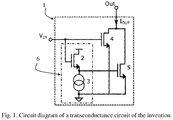
- a transconductance circuit 1 comprises a low g m current source 4, and a high g m current source 5 connected in parallel.
- a voltage drop circuit 6, in this comprising a source follower 2 and a current source 3 for the source follower.
- the bias gate of the (low g m ) current source 4 is connected to the overall input terminal V IN .
- the source follower 2 also has a bias gate linked to V IN , and the current source 3 is linked to the output of the source follower 2.
- the output of the source follower 2 is also connected to the bias gate of the second (high g m ) current source 5.
- the circuit 1 has a single output, Out, from the first (low g m ) current source 4, and second (high g m ) current source 5, connected in parallel.
- the transconductance circuit of the invention may advantageously be employed in any of a range of applications, such as optical receivers, for converting a photodiode current signal to an output signal for downstream processing.
- the width/length of the sources 4 and 5 are 4 ⁇ m/4 ⁇ m, and 80 ⁇ m/0.35 ⁇ m.
- the approximate g m values of the sources 4 and 5 are 50 ⁇ S (micro Siemens) and 15000 ⁇ S for a Vgs voltage of 0.8 Volts.
- the voltage drop circuit 6 may be implemented as a "voltage change" circuit, as the voltage differential across it may be required to change in a predetermined manner. This may involve a linear circuit where the voltage change is implemented by a combination of a resistor with a current source/sink, with the use of an amplifier to buffer the input from any current dissipation, or the use of a non-linear circuit to achieve the required predefined dynamic change.
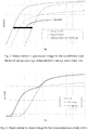
- Fig. 2 shows the output current versus gate source voltage for the two (different sized) MOSFET devices 4 and 5.
- This is a plot of the output current versus Vgs for two unconnected single current mirrors, one with a low g m and the other with a high g m .
- the high g m device outputs a significantly higher current across the full Vgs range, but saturates at a lower Vgs point.
- the accuracy of the high g m device is poor because for a small change in Vgs there is a large change in output current. But with a low g m device the accuracy is better because for a small change in Vgs there is a smaller change in output current.
- Figs. 2 to 4 are plotted versus voltage, whose approximate volts per division is 250mV. Current is plotted on the Y-axis in log format, with a decade increase in each division. In each of these plots the output current of the currents sources is for operation with a fixed drain voltage.
- Fig. 3 is the same as Fig. 2 but includes a high g m device which is operating with a shifted Vgs, so it only turns on at high V IN .
- Fig. 4 this shows combining of the two current mirrors in one circuit. Using a low g m and Vgs shifted high g m current mirror connected in parallel that creates an output current that improves the dynamic range, accuracy and tolerance to mismatch of a single transconductance current source circuit.
- Fig. 5 shows a plot of the possible output current error due to mismatch of identical devices, for three cases versus the output current.
- the three cases being (1) a low g m current mirror, (2) a high g m current mirror and (3) the circuit of the invention.
- the plot shows that the circuit of the invention combines the advantages of the individual low g m current mirror and high g m current mirror - low error due to mismatch and a large dynamic range. It is clear that the low g m device will be accurate for small changes in V IN and tolerant to mismatch, whereas the high g m has the advantage of covering a wide current range.
- the transconductance circuit 1 improves the dynamic range of a single current source, as illustrated in Figs. 3 and 4 , to improve the accuracy at low output currents, as illustrated in Fig. 5 , and ensure it has the dynamic range to output higher currents if required.
- the manner in which the two current sources 4 and 5 are connected to the inputs by the components 2 and 3 is advantageous because it combines the advantages of both a low g m current source 4, and a high g m current source 5 in one circuit.
- Low V IN only the low g m device 4 is on, as the gate source voltage drop across the source follower (2) ensures that the high g m device (5) is off.
- the high g m device 5 is switched on.
- the sizing of the low g m and high g m devices 4 and 5 dictate the accuracy at lower voltage and range at the high voltage, and helps to linearize the output current over the V IN range.
- Fig. 2 shows a comparison between the output current vs. gate source voltage (Vgs) for the low g m and high g m MOSFET devices 4 and 5.
- Vgs output current vs. gate source voltage
- the low g m device can output current from very low values to a nominal maximum value whereas the high g m device can have output a current range up to 100 times the low g m device over the same Vgs range depending on the size difference.
- Fig. 6 shows an example of another embodiment, in which in a circuit 100 the input is connected to the high g m current mirror and a voltage increase circuit can create a voltage higher than the input for the low g m current mirror.
- the operation is the same, as V IN increases the low g m current mirror turns on before the high g m current mirror.
- the benefit of this arrangement is that the circuit operates in a similar manner for a lower input voltage range, which adds flexibility to the use of this circuit.
- a transconductance circuit of the invention has at least two current sources.
- One source is a single current source, which is sized to have low transconductance and to have good accuracy for low output currents, but would have a poor dynamic range.
- the other is a single current source, which is sized to have high g m and a wide dynamic range but poor accuracy for low output current.
- the transconductance circuit 1 combines both of these current sources into one circuit to achieve high accuracy for low output current, a wide dynamic range for high current, and improved the linearity across the range of output currents.
- the transconductance circuit improves the dynamic range (due to the high g m current device), accuracy and tolerance to mismatch of the output current versus a single transconductance current source (due to the low g m current device).
- the linearity of the transconductance is improved versus a single device as shown in Fig. 4 .
- mismatch of a single high g m device can be improved by increasing the area by a large multiple, to achieve the same mismatch error as a single low g m device.
- This generates a single large device, with good dynamic range, good tolerance to mismatch, but has the disadvantages of low speed due to the large capacitance which results from large area.
- a second disadvantage with such a single large area high g m device is that it would have poor output current accuracy at low Vgs, because the g m of this single device still needs to be high to cover the required dynamic range.
- the invention achieves the benefits of such an approach without the associated disadvantages.
- a transconductance circuit of the invention can have more than two current sources connected in parallel, whose objective may be to further linearize the transconductance, or to improve the tolerance to mismatch over a wider range possible than two current sources.
- the outputs may be connected together via a cascode circuit, to improve the speed, noise rejection, or accuracy of the output current.
- the NMOS devices are replaced with PMOS devices, so the output transconductance current sources are now transconductance current sinks.
- NMOS or PMOS MOSFET devices are replaced with NPN or PNP bipolar transistors creating bipolar based output transconductance current sources or current sinks.
- the voltage change circuit may be implemented alternatively than by a source follower and a current source, for example a combination of a resistor with a current source/sink, with the use of an amplifier to buffer the input from any current dissipation.
Landscapes
- Engineering & Computer Science (AREA)
- Power Engineering (AREA)
- Physics & Mathematics (AREA)
- Nonlinear Science (AREA)
- Amplifiers (AREA)
Description
- The invention relates to a transconductance current source.
- Transconductance (gm) is the ratio of the change in current at the output terminal to the change in the voltage at the input terminal of an active device:

- This invention is directed towards providing a circuit that improves the dynamic range, accuracy and tolerance to mismatch of a transconductance current source circuit over a single current source device.
- In many applications where two transconductance current sources are driven by the same voltage, the relative accuracy between the two outputs is important. Accuracy can be achieved by (a) having large area devices or (b) having low gm current sources, so any Vth mismatch in the MOSFETs will have limited effect on the difference in current between the two outputs. Secondly it is beneficial to have low gm devices if the accuracy for small output current changes is important.
- Where a wide range of output current is required, a high gm current source will provide the current, for a limited input voltage (VIN).
-
US5463348 describes transconductance amplifiers with a wide input linear range. -
CN102664597 describes a wide adjustment range transconductance amplifier. -
US5412309 describes current amplifiers. - Other documents describing aspects of transconductance circuits are as follows:
-
US2002/0089377 andUS2011/0298541 describe transconductance circuits with first and second current sources having the same characteristics and comprising a voltage drop circuit with a source follower
and a current source. -
US2011/0316632 describes a CMOS inverter with two transconductances in parallel at the output terminal. -
- [1] A Wide Dynamic Range Continuously Adjustable CMOS Current Mirror, A. K. Gupta, J. W. Haslett, and F. N. Trofimenkoff, IEEE JOURNAL OF SOLID-STATE CIRCUITS, VOL. 31, NO. 8, AUGUST 1996
- [2] Accurate active-feedback CMOS cascode current mirror with improved output swing ALÇI ZEKÇI2 and HAKAN KUNTMAN, INT. J. ELECTRONICS, 1998, VOL. 84, NO. 4, 335-343
- [3] Very Wide Range Tunable CMOS/Bipolar Current Mirrors with Voltage Clamped Input, Teresa Serrano-Gotarredona, Bemab'e Linares-Barranco,and Andreas G. Andreou, IEEE TRANSACTIONS ON CIRCUITS AND SYSTEMS-I: FUNDAMENTAL THEORY AND APPLICATIONS, VOL. 46, NO. 11, NOVEMBER 1999
- We describe a transconductance circuit as set out in
claim 1. - Preferably, each of the current sources is a NMOS or a PMOS MOSFET device or a PNP or an NPN transistor.
- Preferably, the circuit comprises greater than two current sources with different transconductances which are connected in parallel.
- Preferably, an output terminal is linked either directly or via cascodes to the outputs of the first and second current sources.
- We also describe an optical receiver comprising a photodiode and a transconductance circuit of any embodiment linked to said photodiode.
- We also describe a transconductance circuit comprising:
- a first current source with low transconductance and good accuracy for low output currents; and
- a second current source with a high transconductance and a wide dynamic range.
- In one embodiment, the circuit comprises a source follower and a current source for the source follower, in which the input is linked with the gate of the source follower and the first current source.
- In one embodiment, the current sources are configured so that at low input voltage only the low first
current source 4 is on. - In one embodiment, the source follower and the current sources are configured so that a gate-source voltage drop across the source follower ensures that the second current source is off until a point during which the input voltage increases at which the second current source is switched on.
- In one embodiment, the sizing of the first and second current sources dictates the accuracy at lower voltage and range at the high voltage, and helps to linearize the output current over the input voltage range.
- In one embodiment, each of the current sources is a NMOS or a PMOS MOSFET device or a PNP or an NPN transistor.
- In one embodiment, a plurality of devices with low to high transconductances are connected in parallel.
- The invention will be more clearly understood from the following description of some embodiments thereof, given by way of example only with reference to the accompanying drawings in which:-
-
Fig. 1 is a circuit diagram of a transconductance circuit of the invention; -
Fig. 2 is a plot of Log of the output current versus gate-source voltage for the two different size MOSFET devices of current sources of the circuit, with a fixed Vds; -
Fig. 3 is a plot of Log of output current versus gate source voltage for the two different sized MOSFET device and a Vgs shifted MOSFET device, with a fixed Vds; -
Fig. 4 is a plot of Log of the output current versus input voltage for the circuit ofFig. 1 , with a fixed Vds; -
Fig. 5 is a plot of nominal error in current (due to device mismatch) versus output current for single low gm and high gm devices of the circuit; and -
Fig. 6 is a diagram of an alternative transconductance circuit of the invention. - In transconductance circuits a low gm current mirror will output a low current across its Vgs range (small dynamic range) but will have good accuracy and a high tolerance to mismatch. A high gm current mirror of a similar area will output a large current across its Vgs range (high dynamic range) but will have poor accuracy and a low tolerance to mismatch for small lout. Referring to
Fig. 1 atransconductance circuit 1 comprises a low gmcurrent source 4, and a high gmcurrent source 5 connected in parallel. There is avoltage drop circuit 6, in this comprising asource follower 2 and acurrent source 3 for the source follower. The bias gate of the (low gm)current source 4 is connected to the overall input terminal VIN. Thesource follower 2 also has a bias gate linked to VIN, and thecurrent source 3 is linked to the output of thesource follower 2. The output of thesource follower 2 is also connected to the bias gate of the second (high gm)current source 5. Thecircuit 1 has a single output, Out, from the first (low gm)current source 4, and second (high gm)current source 5, connected in parallel. - The transconductance circuit of the invention may advantageously be employed in any of a range of applications, such as optical receivers, for converting a photodiode current signal to an output signal for downstream processing.
- For the examples given here the width/length of the
sources sources - The
voltage drop circuit 6 may be implemented as a "voltage change" circuit, as the voltage differential across it may be required to change in a predetermined manner. This may involve a linear circuit where the voltage change is implemented by a combination of a resistor with a current source/sink, with the use of an amplifier to buffer the input from any current dissipation, or the use of a non-linear circuit to achieve the required predefined dynamic change. -
Fig. 2 shows the output current versus gate source voltage for the two (different sized)MOSFET devices -
Figs. 2 to 4 are plotted versus voltage, whose approximate volts per division is 250mV. Current is plotted on the Y-axis in log format, with a decade increase in each division. In each of these plots the output current of the currents sources is for operation with a fixed drain voltage. -
Fig. 3 is the same asFig. 2 but includes a high gm device which is operating with a shifted Vgs, so it only turns on at high VIN. Referring toFig. 4 , this shows combining of the two current mirrors in one circuit. Using a low gm and Vgs shifted high gm current mirror connected in parallel that creates an output current that improves the dynamic range, accuracy and tolerance to mismatch of a single transconductance current source circuit. -
Fig. 5 shows a plot of the possible output current error due to mismatch of identical devices, for three cases versus the output current. The three cases being (1) a low gm current mirror, (2) a high gm current mirror and (3) the circuit of the invention. The plot shows that the circuit of the invention combines the advantages of the individual low gm current mirror and high gm current mirror - low error due to mismatch and a large dynamic range. It is clear that the low gm device will be accurate for small changes in VIN and tolerant to mismatch, whereas the high gm has the advantage of covering a wide current range. - The
transconductance circuit 1 improves the dynamic range of a single current source, as illustrated inFigs. 3 and 4 , to improve the accuracy at low output currents, as illustrated inFig. 5 , and ensure it has the dynamic range to output higher currents if required. - The manner in which the two
current sources components current source 4, and a high gmcurrent source 5 in one circuit. At low VIN only the low gm device 4 is on, as the gate source voltage drop across the source follower (2) ensures that the high gm device (5) is off. As the VIN increases the high gm device 5 is switched on. The sizing of the low gm and high gm devices 4 and 5 dictate the accuracy at lower voltage and range at the high voltage, and helps to linearize the output current over the VIN range. - In more detail,
Fig. 2 shows a comparison between the output current vs. gate source voltage (Vgs) for the low gm and high gm MOSFET devices 4 and 5. The low gm device can output current from very low values to a nominal maximum value whereas the high gm device can have output a current range up to 100 times the low gm device over the same Vgs range depending on the size difference. -
Fig. 6 shows an example of another embodiment, in which in acircuit 100 the input is connected to the high gm current mirror and a voltage increase circuit can create a voltage higher than the input for the low gm current mirror. The operation is the same, as VIN increases the low gm current mirror turns on before the high gm current mirror. The benefit of this arrangement is that the circuit operates in a similar manner for a lower input voltage range, which adds flexibility to the use of this circuit. - In various embodiments, a transconductance circuit of the invention has at least two current sources. One source is a single current source, which is sized to have low transconductance and to have good accuracy for low output currents, but would have a poor dynamic range. The other is a single current source, which is sized to have high gm and a wide dynamic range but poor accuracy for low output current. The
transconductance circuit 1 combines both of these current sources into one circuit to achieve high accuracy for low output current, a wide dynamic range for high current, and improved the linearity across the range of output currents. - It will be appreciated that the transconductance circuit improves the dynamic range (due to the high gm current device), accuracy and tolerance to mismatch of the output current versus a single transconductance current source (due to the low gm current device). The linearity of the transconductance is improved versus a single device as shown in
Fig. 4 . - It is known in the art that the mismatch of a single high gm device can be improved by increasing the area by a large multiple, to achieve the same mismatch error as a single low gm device. This generates a single large device, with good dynamic range, good tolerance to mismatch, but has the disadvantages of low speed due to the large capacitance which results from large area. A second disadvantage with such a single large area high gm device is that it would have poor output current accuracy at low Vgs, because the gm of this single device still needs to be high to cover the required dynamic range. The invention achieves the benefits of such an approach without the associated disadvantages.
- In various embodiments, a transconductance circuit of the invention can have more than two current sources connected in parallel, whose objective may be to further linearize the transconductance, or to improve the tolerance to mismatch over a wider range possible than two current sources.
- Also, the outputs may be connected together via a cascode circuit, to improve the speed, noise rejection, or accuracy of the output current.
- The invention is not limited to the embodiments described but may be varied in construction and detail.
- For example, in another embodiment of the invention the NMOS devices are replaced with PMOS devices, so the output transconductance current sources are now transconductance current sinks.
- In another embodiment of this invention the NMOS or PMOS MOSFET devices are replaced with NPN or PNP bipolar transistors creating bipolar based output transconductance current sources or current sinks.
- Also, the voltage change circuit may be implemented alternatively than by a source follower and a current source, for example a combination of a resistor with a current source/sink, with the use of an amplifier to buffer the input from any current dissipation.
Claims (5)
- A transconductance circuit comprising:an input terminal (VIN) and an output terminal (Out);a first current source (4) having a gate connected to said input terminal (VIN); anda second current source (5), in parallel with said first current source, and sized differently to have a higher transconductance and a wider dynamic range than the first current source, andwherein the current sources are configured so that at a low input voltage only the first current source (4) is on, and wherein:the transconductance circuit comprises a voltage drop circuit for providing a lower bias voltage for the second current source than for the first current source, the voltage drop circuit comprises a source follower (2) and a current source (3) for the source follower, in which the input terminal is linked with the gate of the source follower (2) and the first current source (4), andthe source follower (2) and the current sources (4, 5) are configured so that a gate-source voltage drop across the source follower (2) ensures that the second current source (5) is off until a point during which the input voltage increases at which the second current source (5) is switched on.
- A transconductance circuit as claimed in claim 1, wherein each of the current sources (4, 5) is a NMOS or a PMOS MOSFET device or a PNP or an NPN transistor.
- A transconductance circuit as claimed in claims 1 or 2, comprising greater than two current sources with different trans conductances which are connected in parallel.
- A transconductance circuit as claimed in any preceding claim, where the output terminal is linked either directly or via cascodes to outputs of the first and second current sources.
- An optical receiver comprising a photodiode and a transconductance circuit of any preceding claim linked to said photodiode.
Applications Claiming Priority (2)
| Application Number | Priority Date | Filing Date | Title |
|---|---|---|---|
| EP15185219 | 2015-09-15 | ||
| PCT/EP2016/071529 WO2017046069A1 (en) | 2015-09-15 | 2016-09-13 | A transconductance current source |
Publications (2)
| Publication Number | Publication Date |
|---|---|
| EP3350920A1 EP3350920A1 (en) | 2018-07-25 |
| EP3350920B1 true EP3350920B1 (en) | 2020-10-07 |
Family
ID=54150254
Family Applications (1)
| Application Number | Title | Priority Date | Filing Date |
|---|---|---|---|
| EP16763849.3A Active EP3350920B1 (en) | 2015-09-15 | 2016-09-13 | A transconductance current source |
Country Status (4)
| Country | Link |
|---|---|
| US (1) | US10218322B2 (en) |
| EP (1) | EP3350920B1 (en) |
| CN (1) | CN108141187A (en) |
| WO (1) | WO2017046069A1 (en) |
Family Cites Families (13)
| Publication number | Priority date | Publication date | Assignee | Title |
|---|---|---|---|---|
| US5412309A (en) | 1993-02-22 | 1995-05-02 | National Semiconductor Corporation | Current amplifiers |
| US5469104A (en) * | 1994-03-28 | 1995-11-21 | Elantec, Inc. | Active folded cascode |
| US5463348A (en) | 1994-07-27 | 1995-10-31 | California Institute Of Technology | CMOS low-power, wide-linear-range, well-input differential and transconductance amplifiers |
| JP3545142B2 (en) * | 1996-11-25 | 2004-07-21 | 三菱電機株式会社 | Differential amplifier |
| KR20020035324A (en) | 2000-11-06 | 2002-05-11 | 김덕중 | Differential amplifier |
| US7193464B2 (en) * | 2000-12-15 | 2007-03-20 | Broadcom Corporation | Differential amplifier with large input common mode signal range |
| AU2002256613A1 (en) * | 2002-01-21 | 2003-07-30 | Optillion Ab | Input circuit |
| DE10239813B4 (en) * | 2002-08-29 | 2005-09-29 | Advanced Micro Devices, Inc., Sunnyvale | Electronic circuit with improved current stabilization |
| US7187236B2 (en) * | 2004-09-07 | 2007-03-06 | Ut-Battelle, Llc | Rail-to-rail differential input amplification stage with main and surrogate differential pairs |
| US8445832B2 (en) | 2009-03-05 | 2013-05-21 | Hitachi, Ltd. | Optical communication device |
| US8102211B2 (en) * | 2010-06-08 | 2012-01-24 | Qualcomm, Incorporated | Rail-to-rail input stage circuit with dynamic bias control |
| CN102664597A (en) | 2012-04-26 | 2012-09-12 | 无锡中科微电子工业技术研究院有限责任公司 | Wide-adjustment-range transconductance amplifier based on digital control technology and control method thereof |
| CN103825566B (en) * | 2012-11-16 | 2018-03-20 | 凌朝东 | The high linearity optimization method of trsanscondutance amplifier |
-
2016
- 2016-09-13 CN CN201680061333.2A patent/CN108141187A/en active Pending
- 2016-09-13 EP EP16763849.3A patent/EP3350920B1/en active Active
- 2016-09-13 WO PCT/EP2016/071529 patent/WO2017046069A1/en not_active Ceased
- 2016-09-13 US US15/759,404 patent/US10218322B2/en active Active
Non-Patent Citations (1)
| Title |
|---|
| None * |
Also Published As
| Publication number | Publication date |
|---|---|
| EP3350920A1 (en) | 2018-07-25 |
| US10218322B2 (en) | 2019-02-26 |
| CN108141187A (en) | 2018-06-08 |
| WO2017046069A1 (en) | 2017-03-23 |
| US20180212575A1 (en) | 2018-07-26 |
Similar Documents
| Publication | Publication Date | Title |
|---|---|---|
| US7994858B2 (en) | Operational trans-conductance amplifier with output clamp circuit | |
| US9438175B2 (en) | Cascode amplifier | |
| KR101485725B1 (en) | System | |
| US9214929B2 (en) | Waveform conversion circuit with reduced jitter | |
| US10914761B2 (en) | Voltage detector | |
| US7872519B2 (en) | Voltage divider circuit | |
| US11005428B2 (en) | Differential input circuit, amplification circuit, and display apparatus | |
| JP2011155488A (en) | Differential input stage circuit, operational amplifier including the same, and voltage regulator circuit | |
| US20150137858A1 (en) | Buffer circuit | |
| KR102532834B1 (en) | Voltage regulator | |
| JP2002185272A (en) | Differential amplifier | |
| TWI548209B (en) | Differential operational amplifier and bandgap reference voltage generating circuit | |
| KR102483031B1 (en) | Current generating circuit | |
| US9811105B2 (en) | Reference voltage circuit | |
| US9543905B2 (en) | Amplifier circuit | |
| US8723593B2 (en) | Bias voltage generation circuit and differential circuit | |
| KR20180111577A (en) | Transconductance amplifier | |
| JP2010233084A (en) | Differential amplifier | |
| US10218322B2 (en) | Transconductance current source | |
| US10110171B2 (en) | Amplifier | |
| US9847758B2 (en) | Low noise amplifier | |
| KR20170097121A (en) | Differential comparator | |
| Khan | Design analysis and performance comparison of low power high gain 2nd stage differential amplifier along with 1st stage | |
| CN103543776A (en) | voltage buffer | |
| JP5592334B2 (en) | Splitter circuit |
Legal Events
| Date | Code | Title | Description |
|---|---|---|---|
| STAA | Information on the status of an ep patent application or granted ep patent |
Free format text: STATUS: THE INTERNATIONAL PUBLICATION HAS BEEN MADE |
|
| PUAI | Public reference made under article 153(3) epc to a published international application that has entered the european phase |
Free format text: ORIGINAL CODE: 0009012 |
|
| STAA | Information on the status of an ep patent application or granted ep patent |
Free format text: STATUS: REQUEST FOR EXAMINATION WAS MADE |
|
| 17P | Request for examination filed |
Effective date: 20180410 |
|
| AK | Designated contracting states |
Kind code of ref document: A1 Designated state(s): AL AT BE BG CH CY CZ DE DK EE ES FI FR GB GR HR HU IE IS IT LI LT LU LV MC MK MT NL NO PL PT RO RS SE SI SK SM TR |
|
| AX | Request for extension of the european patent |
Extension state: BA ME |
|
| DAV | Request for validation of the european patent (deleted) | ||
| DAX | Request for extension of the european patent (deleted) | ||
| GRAP | Despatch of communication of intention to grant a patent |
Free format text: ORIGINAL CODE: EPIDOSNIGR1 |
|
| STAA | Information on the status of an ep patent application or granted ep patent |
Free format text: STATUS: GRANT OF PATENT IS INTENDED |
|
| INTG | Intention to grant announced |
Effective date: 20191205 |
|
| GRAS | Grant fee paid |
Free format text: ORIGINAL CODE: EPIDOSNIGR3 |
|
| GRAA | (expected) grant |
Free format text: ORIGINAL CODE: 0009210 |
|
| STAA | Information on the status of an ep patent application or granted ep patent |
Free format text: STATUS: THE PATENT HAS BEEN GRANTED |
|
| AK | Designated contracting states |
Kind code of ref document: B1 Designated state(s): AL AT BE BG CH CY CZ DE DK EE ES FI FR GB GR HR HU IE IS IT LI LT LU LV MC MK MT NL NO PL PT RO RS SE SI SK SM TR |
|
| REG | Reference to a national code |
Ref country code: GB Ref legal event code: FG4D |
|
| REG | Reference to a national code |
Ref country code: CH Ref legal event code: EP Ref country code: AT Ref legal event code: REF Ref document number: 1322254 Country of ref document: AT Kind code of ref document: T Effective date: 20201015 |
|
| REG | Reference to a national code |
Ref country code: IE Ref legal event code: FG4D |
|
| REG | Reference to a national code |
Ref country code: DE Ref legal event code: R096 Ref document number: 602016045429 Country of ref document: DE |
|
| REG | Reference to a national code |
Ref country code: NL Ref legal event code: MP Effective date: 20201007 |
|
| REG | Reference to a national code |
Ref country code: AT Ref legal event code: MK05 Ref document number: 1322254 Country of ref document: AT Kind code of ref document: T Effective date: 20201007 |
|
| PG25 | Lapsed in a contracting state [announced via postgrant information from national office to epo] |
Ref country code: FI Free format text: LAPSE BECAUSE OF FAILURE TO SUBMIT A TRANSLATION OF THE DESCRIPTION OR TO PAY THE FEE WITHIN THE PRESCRIBED TIME-LIMIT Effective date: 20201007 Ref country code: GR Free format text: LAPSE BECAUSE OF FAILURE TO SUBMIT A TRANSLATION OF THE DESCRIPTION OR TO PAY THE FEE WITHIN THE PRESCRIBED TIME-LIMIT Effective date: 20210108 Ref country code: RS Free format text: LAPSE BECAUSE OF FAILURE TO SUBMIT A TRANSLATION OF THE DESCRIPTION OR TO PAY THE FEE WITHIN THE PRESCRIBED TIME-LIMIT Effective date: 20201007 Ref country code: PT Free format text: LAPSE BECAUSE OF FAILURE TO SUBMIT A TRANSLATION OF THE DESCRIPTION OR TO PAY THE FEE WITHIN THE PRESCRIBED TIME-LIMIT Effective date: 20210208 Ref country code: NO Free format text: LAPSE BECAUSE OF FAILURE TO SUBMIT A TRANSLATION OF THE DESCRIPTION OR TO PAY THE FEE WITHIN THE PRESCRIBED TIME-LIMIT Effective date: 20210107 |
|
| REG | Reference to a national code |
Ref country code: LT Ref legal event code: MG4D |
|
| PG25 | Lapsed in a contracting state [announced via postgrant information from national office to epo] |
Ref country code: ES Free format text: LAPSE BECAUSE OF FAILURE TO SUBMIT A TRANSLATION OF THE DESCRIPTION OR TO PAY THE FEE WITHIN THE PRESCRIBED TIME-LIMIT Effective date: 20201007 Ref country code: AT Free format text: LAPSE BECAUSE OF FAILURE TO SUBMIT A TRANSLATION OF THE DESCRIPTION OR TO PAY THE FEE WITHIN THE PRESCRIBED TIME-LIMIT Effective date: 20201007 Ref country code: PL Free format text: LAPSE BECAUSE OF FAILURE TO SUBMIT A TRANSLATION OF THE DESCRIPTION OR TO PAY THE FEE WITHIN THE PRESCRIBED TIME-LIMIT Effective date: 20201007 Ref country code: IS Free format text: LAPSE BECAUSE OF FAILURE TO SUBMIT A TRANSLATION OF THE DESCRIPTION OR TO PAY THE FEE WITHIN THE PRESCRIBED TIME-LIMIT Effective date: 20210207 Ref country code: LV Free format text: LAPSE BECAUSE OF FAILURE TO SUBMIT A TRANSLATION OF THE DESCRIPTION OR TO PAY THE FEE WITHIN THE PRESCRIBED TIME-LIMIT Effective date: 20201007 Ref country code: BG Free format text: LAPSE BECAUSE OF FAILURE TO SUBMIT A TRANSLATION OF THE DESCRIPTION OR TO PAY THE FEE WITHIN THE PRESCRIBED TIME-LIMIT Effective date: 20210107 Ref country code: SE Free format text: LAPSE BECAUSE OF FAILURE TO SUBMIT A TRANSLATION OF THE DESCRIPTION OR TO PAY THE FEE WITHIN THE PRESCRIBED TIME-LIMIT Effective date: 20201007 |
|
| PG25 | Lapsed in a contracting state [announced via postgrant information from national office to epo] |
Ref country code: NL Free format text: LAPSE BECAUSE OF FAILURE TO SUBMIT A TRANSLATION OF THE DESCRIPTION OR TO PAY THE FEE WITHIN THE PRESCRIBED TIME-LIMIT Effective date: 20201007 Ref country code: HR Free format text: LAPSE BECAUSE OF FAILURE TO SUBMIT A TRANSLATION OF THE DESCRIPTION OR TO PAY THE FEE WITHIN THE PRESCRIBED TIME-LIMIT Effective date: 20201007 |
|
| REG | Reference to a national code |
Ref country code: DE Ref legal event code: R097 Ref document number: 602016045429 Country of ref document: DE |
|
| PG25 | Lapsed in a contracting state [announced via postgrant information from national office to epo] |
Ref country code: RO Free format text: LAPSE BECAUSE OF FAILURE TO SUBMIT A TRANSLATION OF THE DESCRIPTION OR TO PAY THE FEE WITHIN THE PRESCRIBED TIME-LIMIT Effective date: 20201007 Ref country code: SK Free format text: LAPSE BECAUSE OF FAILURE TO SUBMIT A TRANSLATION OF THE DESCRIPTION OR TO PAY THE FEE WITHIN THE PRESCRIBED TIME-LIMIT Effective date: 20201007 Ref country code: EE Free format text: LAPSE BECAUSE OF FAILURE TO SUBMIT A TRANSLATION OF THE DESCRIPTION OR TO PAY THE FEE WITHIN THE PRESCRIBED TIME-LIMIT Effective date: 20201007 Ref country code: CZ Free format text: LAPSE BECAUSE OF FAILURE TO SUBMIT A TRANSLATION OF THE DESCRIPTION OR TO PAY THE FEE WITHIN THE PRESCRIBED TIME-LIMIT Effective date: 20201007 Ref country code: LT Free format text: LAPSE BECAUSE OF FAILURE TO SUBMIT A TRANSLATION OF THE DESCRIPTION OR TO PAY THE FEE WITHIN THE PRESCRIBED TIME-LIMIT Effective date: 20201007 Ref country code: SM Free format text: LAPSE BECAUSE OF FAILURE TO SUBMIT A TRANSLATION OF THE DESCRIPTION OR TO PAY THE FEE WITHIN THE PRESCRIBED TIME-LIMIT Effective date: 20201007 |
|
| PLBE | No opposition filed within time limit |
Free format text: ORIGINAL CODE: 0009261 |
|
| STAA | Information on the status of an ep patent application or granted ep patent |
Free format text: STATUS: NO OPPOSITION FILED WITHIN TIME LIMIT |
|
| PG25 | Lapsed in a contracting state [announced via postgrant information from national office to epo] |
Ref country code: DK Free format text: LAPSE BECAUSE OF FAILURE TO SUBMIT A TRANSLATION OF THE DESCRIPTION OR TO PAY THE FEE WITHIN THE PRESCRIBED TIME-LIMIT Effective date: 20201007 |
|
| 26N | No opposition filed |
Effective date: 20210708 |
|
| PG25 | Lapsed in a contracting state [announced via postgrant information from national office to epo] |
Ref country code: AL Free format text: LAPSE BECAUSE OF FAILURE TO SUBMIT A TRANSLATION OF THE DESCRIPTION OR TO PAY THE FEE WITHIN THE PRESCRIBED TIME-LIMIT Effective date: 20201007 Ref country code: IT Free format text: LAPSE BECAUSE OF FAILURE TO SUBMIT A TRANSLATION OF THE DESCRIPTION OR TO PAY THE FEE WITHIN THE PRESCRIBED TIME-LIMIT Effective date: 20201007 |
|
| PG25 | Lapsed in a contracting state [announced via postgrant information from national office to epo] |
Ref country code: SI Free format text: LAPSE BECAUSE OF FAILURE TO SUBMIT A TRANSLATION OF THE DESCRIPTION OR TO PAY THE FEE WITHIN THE PRESCRIBED TIME-LIMIT Effective date: 20201007 |
|
| REG | Reference to a national code |
Ref country code: CH Ref legal event code: PL |
|
| REG | Reference to a national code |
Ref country code: BE Ref legal event code: MM Effective date: 20210930 |
|
| GBPC | Gb: european patent ceased through non-payment of renewal fee |
Effective date: 20210913 |
|
| PG25 | Lapsed in a contracting state [announced via postgrant information from national office to epo] |
Ref country code: IS Free format text: LAPSE BECAUSE OF FAILURE TO SUBMIT A TRANSLATION OF THE DESCRIPTION OR TO PAY THE FEE WITHIN THE PRESCRIBED TIME-LIMIT Effective date: 20210207 Ref country code: MC Free format text: LAPSE BECAUSE OF FAILURE TO SUBMIT A TRANSLATION OF THE DESCRIPTION OR TO PAY THE FEE WITHIN THE PRESCRIBED TIME-LIMIT Effective date: 20201007 |
|
| PG25 | Lapsed in a contracting state [announced via postgrant information from national office to epo] |
Ref country code: LU Free format text: LAPSE BECAUSE OF NON-PAYMENT OF DUE FEES Effective date: 20210913 Ref country code: IE Free format text: LAPSE BECAUSE OF NON-PAYMENT OF DUE FEES Effective date: 20210913 Ref country code: GB Free format text: LAPSE BECAUSE OF NON-PAYMENT OF DUE FEES Effective date: 20210913 Ref country code: FR Free format text: LAPSE BECAUSE OF NON-PAYMENT OF DUE FEES Effective date: 20210930 Ref country code: BE Free format text: LAPSE BECAUSE OF NON-PAYMENT OF DUE FEES Effective date: 20210930 |
|
| PG25 | Lapsed in a contracting state [announced via postgrant information from national office to epo] |
Ref country code: LI Free format text: LAPSE BECAUSE OF NON-PAYMENT OF DUE FEES Effective date: 20210930 Ref country code: CH Free format text: LAPSE BECAUSE OF NON-PAYMENT OF DUE FEES Effective date: 20210930 |
|
| PG25 | Lapsed in a contracting state [announced via postgrant information from national office to epo] |
Ref country code: HU Free format text: LAPSE BECAUSE OF FAILURE TO SUBMIT A TRANSLATION OF THE DESCRIPTION OR TO PAY THE FEE WITHIN THE PRESCRIBED TIME-LIMIT; INVALID AB INITIO Effective date: 20160913 |
|
| P01 | Opt-out of the competence of the unified patent court (upc) registered |
Effective date: 20230413 |
|
| PG25 | Lapsed in a contracting state [announced via postgrant information from national office to epo] |
Ref country code: CY Free format text: LAPSE BECAUSE OF FAILURE TO SUBMIT A TRANSLATION OF THE DESCRIPTION OR TO PAY THE FEE WITHIN THE PRESCRIBED TIME-LIMIT Effective date: 20201007 |
|
| PG25 | Lapsed in a contracting state [announced via postgrant information from national office to epo] |
Ref country code: MK Free format text: LAPSE BECAUSE OF FAILURE TO SUBMIT A TRANSLATION OF THE DESCRIPTION OR TO PAY THE FEE WITHIN THE PRESCRIBED TIME-LIMIT Effective date: 20201007 |
|
| PG25 | Lapsed in a contracting state [announced via postgrant information from national office to epo] |
Ref country code: TR Free format text: LAPSE BECAUSE OF FAILURE TO SUBMIT A TRANSLATION OF THE DESCRIPTION OR TO PAY THE FEE WITHIN THE PRESCRIBED TIME-LIMIT Effective date: 20201007 |
|
| PG25 | Lapsed in a contracting state [announced via postgrant information from national office to epo] |
Ref country code: MT Free format text: LAPSE BECAUSE OF FAILURE TO SUBMIT A TRANSLATION OF THE DESCRIPTION OR TO PAY THE FEE WITHIN THE PRESCRIBED TIME-LIMIT Effective date: 20201007 |
|
| PGFP | Annual fee paid to national office [announced via postgrant information from national office to epo] |
Ref country code: DE Payment date: 20250811 Year of fee payment: 10 |