EP3349318B1 - Surge protection device base - Google Patents
Surge protection device base Download PDFInfo
- Publication number
- EP3349318B1 EP3349318B1 EP16843645.9A EP16843645A EP3349318B1 EP 3349318 B1 EP3349318 B1 EP 3349318B1 EP 16843645 A EP16843645 A EP 16843645A EP 3349318 B1 EP3349318 B1 EP 3349318B1
- Authority
- EP
- European Patent Office
- Prior art keywords
- housing
- protection device
- surge protection
- device base
- half side
- Prior art date
- Legal status (The legal status is an assumption and is not a legal conclusion. Google has not performed a legal analysis and makes no representation as to the accuracy of the status listed.)
- Active
Links
Images




Classifications
-
- H—ELECTRICITY
- H02—GENERATION; CONVERSION OR DISTRIBUTION OF ELECTRIC POWER
- H02H—EMERGENCY PROTECTIVE CIRCUIT ARRANGEMENTS
- H02H9/00—Emergency protective circuit arrangements for limiting excess current or voltage without disconnection
- H02H9/04—Emergency protective circuit arrangements for limiting excess current or voltage without disconnection responsive to excess voltage
-
- H—ELECTRICITY
- H01—ELECTRIC ELEMENTS
- H01C—RESISTORS
- H01C7/00—Non-adjustable resistors formed as one or more layers or coatings; Non-adjustable resistors made from powdered conducting material or powdered semi-conducting material with or without insulating material
- H01C7/10—Non-adjustable resistors formed as one or more layers or coatings; Non-adjustable resistors made from powdered conducting material or powdered semi-conducting material with or without insulating material voltage responsive, i.e. varistors
- H01C7/12—Overvoltage protection resistors; Arresters
-
- H—ELECTRICITY
- H01—ELECTRIC ELEMENTS
- H01C—RESISTORS
- H01C7/00—Non-adjustable resistors formed as one or more layers or coatings; Non-adjustable resistors made from powdered conducting material or powdered semi-conducting material with or without insulating material
- H01C7/02—Non-adjustable resistors formed as one or more layers or coatings; Non-adjustable resistors made from powdered conducting material or powdered semi-conducting material with or without insulating material having positive temperature coefficient
- H01C7/022—Non-adjustable resistors formed as one or more layers or coatings; Non-adjustable resistors made from powdered conducting material or powdered semi-conducting material with or without insulating material having positive temperature coefficient mainly consisting of non-metallic substances
Definitions
- the present invention relates to a field of low voltage electric apparatus, more particularly, relates to a surge protection device base and to a surge protection device.
- a surge protection device is usually used by a technical person in the field to protect overvoltage induced by thunder in a low voltage power distribution system. Generally, it is required to cut off a circuit of the whole system for replacing the surge protection device, so that normal equipment in the system will stop operation, which will cause adverse effects on manufacturing and daily life.
- a damaged overvoltage protector may be replaced by replacing the pluggable module without cutting off the circuit of the whole system. The replacement operation is simple and efficient.
- the existing pluggable surge protection devices basically have two types of bases: an integral type and an assembled type.
- the integral type has a complete structure, good appearance and good structural strength, but different bases corresponding to respective poles need to be developed separately.
- the integral type has a low repeatability and high cost (the universality of elements is low so that the cost is high).
- the assembled type only develops a unipolar base, and a multipolar base is formed through mechanical splicing of a plurality of unipolar bases.
- the assembled type base has obvious gaps between poles and poor integrity, and an external bus bar is required to connect the respective poles.
- the assembled type is complex in operation and poor in appearance.
- a multipolar base formed by splicing of unipolar bases has poor integrity and is not able to achieve pre-wiring.
- FIG. 1 illustrates a structural diagram of a multipolar base formed by mechanically splicing a plurality of unipolar bases according to prior art.
- JP 2011 108559 A describes an electrical equipment equipped with incorrect connection prevention mechanism composed of a terminal device and a plug connected to the terminal device.
- a case side incorrect connection prevention piece is mounted on a vertical inner wall of one case vertical portion of facing case vertical portion in the terminal device
- a plug side incorrect connection prevention piece is mounted on one vertical side wall of a vertical side wall faced by the plug.
- the case side incorrect connection prevention piece and the plug side incorrect connection prevention piece are opposed, into a plug fitting recess portion of the terminal device, when the plug is fitted, the case side incorrect connection prevention piece and the plug side incorrect connection prevention piece become to have a normal fitting state.
- the combined type surge protector connection structure comprises one-pole type surge protectors, wherein a surge protection module of each one-pole surge protector is respectively assembled in a base of the one-pole type surge protector, a connection end of one end of each base is embedded with a busbar, a side wall of each busbar is sleeved with an insulation sleeve casing, the other end of the base is respectively arranged with an inward concave long groove, fasteners are mounted between the adjacent inward concave long grooves, a connection portion of each busbar and the surge protection module of each one-pole surge protector is respectively arranged with an inward concave circular groove, a caliber of a notch of the inward concave circular groove is smaller than that of the inward concave circular groove, and each inward concave circular groove is locked and connected with the connection end of one end of each base through a locking piece.
- a surge protection device base as defined in claim 1 is provided.
- the surge protection device base comprises a first housing, a second housing and at least one third housing.
- the first housing comprises at least one first structure.
- the second housing comprises at least one second structure.
- the third housing is arranged between the first housing and the second housing and comprises a first half side and a second half side.
- the first housing, one or more third housings and the second housing are spliced together to form a multipolar surge protection device base.
- the first housing and the first half side of the third housing adjacent thereto constitute an unipolar surge protection device base
- the second half side and the first half side of two adjacent third housings constitute an unipolar surge protection device base
- the second housing and the second half side of the third housing adjacent thereto constitute an unipolar surge protection device base.
- the first structure corresponds to an element positioned within the first housing and the second half side of the third housing.
- the second structure corresponds to an element positioned within the second housing and the first half side of the third housing.
- Through holes are formed in the third housing at corresponding positions, so as to install connected elements used for a multipolar surge protection device.
- a first through hole formed at a first end of the bottom of the third housing is configured to accommodate a connected bus bar.
- a second through hole formed at a second end of the bottom of the third housing is configured to accommodate a connected microswitch.
- the first housing and a first one of the third housings, two third housings, a second one of the third housings and the second housing are spliced with each other through holes-shafts and/or stepped slots.
- the first structure comprises a microswitch slot which corresponds to a microswitch positioned in the first housing and the second side half of the third housing.
- the second structure comprises an execution rod slot which corresponds to a remote signaling alarm execution mechanism positioned in the second housing and the first half side of the third housing.
- an unipolar or multipolar surge protection device base is directly formed through splicing of different components.
- elements such as wiring terminal, bus bar and microswitch etc. can be installed inside the base of the surge protection device, so that integrality and attractiveness are achieved, and cost is reduced.
- the invention also provides a surge protection device as defined in claim 4.
- the invention provides a spliced surge protection device base, a unipolar or multipolar surge protection device base can be directly formed through splicing of components.
- FIG. 2a and FIG. 2b illustrate a surge protection device base which may form part of a surge protection device base according to an example in the present invention.
- FIG. 2a and FIG. 2b illustrate a unipolar surge protection device base.
- the surge protection device base comprises a first housing 101 and a second housing 102.
- the first housing 101 and the second housing 102 are spliced together to form a unipolar surge protection device base 121.
- the first housing 101 and the second housing 102 are combined in a left-right splicing mode to form a complete surge protection base 121.
- the first housing and the second housing are spliced with each other through holes-shafts and/or stepped slots.
- the first housing and the second housing may be spliced in other manners which are appropriate.
- Various elements of the surge protection device are accommodated in the surge protection device base 121. Some elements need to be in contact with or connected with external component, so the surge protection device base 121 is provided with structures corresponding to these elements. Because the installation positions of these elements in the surge protection device base are different, the first housing and the second housing are respectively provided with structures corresponding to the elements installed inside the first housing or the second housing.
- the first housing 101 is provided with a first structure corresponding to an element positioned within the first housing.
- the second housing 102 is provided with a second structure corresponding to an element positioned within the second housing.
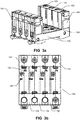
- FIG. 3a and FIG. 3b illustrate a surge protection device base according to an embodiment of the present invention.
- FIG. 3a and FIG. 3b illustrate a multipolar surge protection device base.
- the surge protection device base of the present invention when a multipolar base is formed, components are assembled directly to form an integrated multipolar base, rather than mechanical splicing of a plurality of unipolar bases.
- the surge protection device base comprises a first housing 101, a second housing 102 and a third housing 103.
- One first housing 101, one or more third housings 103 and one second housing 102 are spliced together to form a multipolar surge protection device base 122.
- one or more third housings 103 are inserted between the first housing 101 and the second housing 102.
- the first housing 101 is also provided with at least one first structure
- the second housing 102 is also provided with at least one second structure.
- the third housing 103 is divided into two half sides: a first half side and a second half side.
- the third housing 103 is provided with at least one first structure and at least one second structure, the first structure is positioned at the second half side of the third housing while the second structure is positioned at the first half side of the third housing.
- a second half side and a first half side of the two adjacent third housings constitute a unipolar surge protection device base.
- the second housing and a second half side of the third housing adjacent thereto constitute a unipolar surge protection device base. That is, although the third housing is a component itself, it is used to form a unipolar base with adjacent components.
- the half sides of the third housing can be spliced with the first housing or the second housing respectively to form a unipolar base, or different half sides of two third housings can be spliced to form a unipolar base.
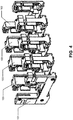
- FIG. 4 illustrates an exploded structural diagram of a surge protection device base according to an embodiment of the present invention.
- FIG. 4 illustrates a multipolar surge protection device base.
- the first housing and the third housing, the two third housings, the third housing and the second housing are spliced with each other through holes-shafts and/or stepped slots.
- the first housing and the third housing, the two third housings, the third housing and the second housing may be spliced in other manners which are appropriate.
- the first structure positioned on the first housing or the third housing corresponds to an element positioned within the first housing and the second half side of the third housing.
- the first housing and the second half side of the third housing are the same side, so that the elements arranged therein are the same.
- the second structure positioned on the second housing or the third housing corresponds to an element positioned within the second housing and the first half side of the third housing.
- the second housing and the first half side of the third housing are the same side, so that the elements arranged therein are the same.
- the third housing 103 is always located between the first housing 101 and the second housing 102 and will not be exposed outside, so that through holes can be formed in the third housing 103 to install connected elements for a multipolar surge protection device.
- the connected elements such as a plurality of microswitches used for a multipolar surge protection device, an integrated bus bar used for a multipolar surge protection device can be installed in the through hole. Connection of the plurality of elements used for the multipolar surge protection device can save the installation cost and reduce the installation difficulty, which can reduce an overall cost.
- the through holes in the third housing will be shielded by the first housing and the second housing, so that an overall attractiveness will not be influenced by the through holes formed in the third housing.
- FIG. 5 illustrates a schematic diagram of accommodation of a bus bar of a surge protection device base according to an embodiment of the present invention.
- a first through hole 104 is formed at a first end of the bottom of the third housing for accommodating a connected bus bar 107.
- the bus bar 107 is integrated and is formed by processing of an integral metal sheet.
- a U-shaped structure 172 is formed at the bottom of the bus bar 107, the U-shaped structure 172 accommodates a connector 173 which is used for contacting with a pin.
- the connector 173 is elastic so as to clamp the pin.
- both ends of the bottom of the third housing are provided with first through holes 104 for accommodating the bus bar.
- both ends of the top of the third housing are provided with openings for inserting the pins. The positions of the openings correspond to the positions of the bus bar and the connectors.
- FIG. 6 illustrates a schematic diagram of accommodation of a microswitch of a surge protection device base according to an embodiment of the present invention.
- a second through hole is formed at a second end of the bottom of the third housing 103 for accommodating a connected microswitch.
- the connected microswitch constitutes a remote signaling alarm device of the surge protection device.
- the remote signaling alarm device is composed of a circuit board 181 and microswitches 182, and is connected with wiring terminals through wires.
- the microswitches 182 for respective poles are mounted on a same circuit board 181, for example, a plurality of microswitches 182 are welded on the circuit board 181.
- Each microswitch 182 corresponds to the position of the surge protection device of a respective pole.
- the circuit board 181 and the microswitches 182 mounted thereon are integrally loaded into the second through hole.
- the microswitch 182 is located at a position where the first housing or the second half side of the third housing is located, so that a microswitch slot 188 is formed in the first housing or the second half side of the third housing (refer to FIG. 2b ) for accommodating an operation button of the microswitch.
- the microswitch slot 188 is an example of the so-called first structure.
- the remote signaling alarm device further comprises an execution mechanism, according to an embodiment, the execution mechanism is an execution rod 109.
- FIG. 7a and FIG. 7b illustrate schematic diagrams of accommodation of a remote signaling alarm execution mechanism of a surge protection device base according to an embodiment of the present invention.
- the execution rod 109 is rotatably mounted in a slot hole 106 through a shaft at an end of the execution rod 109.
- the slot hole 106 is located on the second housing 102 or the first half side of the third housing 103.
- the slot hole 106 shown in FIG. 7A is located on the second housing 102
- the slot hole 106 shown in FIG. 7B is located on the first half side of the third housing 103.
- the slot hole 106 is an example of the so-called second structure.
- the other end of the execution rod 109 forms a protrusion, the position of the protrusion corresponds to an execution rod slot 199 on the housing (see FIG. 2b ).
- the execution rod slot 199 is also an example of the so-called second structure.
- a working process of the remote signaling alarm device is as follows: an overvoltage protection module is inserted into the base of the surge protection device and a bottom of the overvoltage protection module is in contact with the protrusion of the executing rod 109.
- the overvoltage protection module When the overvoltage protection module is in a working state, the bottom of the overvoltage protection module applies a force to press down the protrusion of the execution rod 109.
- the execution rod 109 is pressed down along with the protrusion as well, then the microswitch 182 is pressed down and in an energy storage state.
- the overvoltage protection module is pulled out or in a fault state, the bottom of the overvoltage protection module no longer applies the force to the protrusion of the execution rod 109, and the force applied by the execution rod 109 to the microswitch 182 does not exist as well. Then the microswitch 182 is bounced off by the energy stored by itself. The execution rod 109 is lifted upwards and the microswitch 182 is restored to the original position.
- a unipolar or multipolar surge protection device base is directly formed through splicing of different components.
- elements such as wiring terminal, bus bar and microswitch etc. can be installed inside the base of the surge protection device, so that integrality and attractiveness are achieved, and cost is reduced.
Landscapes
- Engineering & Computer Science (AREA)
- Microelectronics & Electronic Packaging (AREA)
- Physics & Mathematics (AREA)
- Electromagnetism (AREA)
- Emergency Protection Circuit Devices (AREA)
Description
- The present invention relates to a field of low voltage electric apparatus, more particularly, relates to a surge protection device base and to a surge protection device.
- A surge protection device (SPD) is usually used by a technical person in the field to protect overvoltage induced by thunder in a low voltage power distribution system. Generally, it is required to cut off a circuit of the whole system for replacing the surge protection device, so that normal equipment in the system will stop operation, which will cause adverse effects on manufacturing and daily life. Through a pluggable cooperation mode of a pluggable overvoltage protection module and a base for accommodating the protection module, a damaged overvoltage protector may be replaced by replacing the pluggable module without cutting off the circuit of the whole system. The replacement operation is simple and efficient.
- The existing pluggable surge protection devices basically have two types of bases: an integral type and an assembled type. The integral type has a complete structure, good appearance and good structural strength, but different bases corresponding to respective poles need to be developed separately. The integral type has a low repeatability and high cost (the universality of elements is low so that the cost is high). The assembled type only develops a unipolar base, and a multipolar base is formed through mechanical splicing of a plurality of unipolar bases. The assembled type base has obvious gaps between poles and poor integrity, and an external bus bar is required to connect the respective poles. The assembled type is complex in operation and poor in appearance. A multipolar base formed by splicing of unipolar bases has poor integrity and is not able to achieve pre-wiring. Each unipolar base is electrically independent and an external electrical connection is required to connect them to be electrically integral, which would cause troubles to the user during installation and wiring.
FIG. 1 illustrates a structural diagram of a multipolar base formed by mechanically splicing a plurality of unipolar bases according to prior art. -
JP 2011 108559 A -
CN 202 737113 U describes a combined type surge protector connection structure. The combined type surge protector connection structure comprises one-pole type surge protectors, wherein a surge protection module of each one-pole surge protector is respectively assembled in a base of the one-pole type surge protector, a connection end of one end of each base is embedded with a busbar, a side wall of each busbar is sleeved with an insulation sleeve casing, the other end of the base is respectively arranged with an inward concave long groove, fasteners are mounted between the adjacent inward concave long grooves, a connection portion of each busbar and the surge protection module of each one-pole surge protector is respectively arranged with an inward concave circular groove, a caliber of a notch of the inward concave circular groove is smaller than that of the inward concave circular groove, and each inward concave circular groove is locked and connected with the connection end of one end of each base through a locking piece. - According to an embodiment of the present invention, a surge protection device base as defined in claim 1 is provided. The surge protection device base comprises a first housing, a second housing and at least one third housing. The first housing comprises at least one first structure. The second housing comprises at least one second structure. The third housing is arranged between the first housing and the second housing and comprises a first half side and a second half side. The first housing, one or more third housings and the second housing are spliced together to form a multipolar surge protection device base. The first housing and the first half side of the third housing adjacent thereto constitute an unipolar surge protection device base, the second half side and the first half side of two adjacent third housings constitute an unipolar surge protection device base, and the second housing and the second half side of the third housing adjacent thereto constitute an unipolar surge protection device base. The first structure corresponds to an element positioned within the first housing and the second half side of the third housing. The second structure corresponds to an element positioned within the second housing and the first half side of the third housing. Through holes are formed in the third housing at corresponding positions, so as to install connected elements used for a multipolar surge protection device. A first through hole formed at a first end of the bottom of the third housing is configured to accommodate a connected bus bar. A second through hole formed at a second end of the bottom of the third housing is configured to accommodate a connected microswitch.
- According to an embodiment, the first housing and a first one of the third housings, two third housings, a second one of the third housings and the second housing are spliced with each other through holes-shafts and/or stepped slots.
- According to an embodiment, the first structure comprises a microswitch slot which corresponds to a microswitch positioned in the first housing and the second side half of the third housing. The second structure comprises an execution rod slot which corresponds to a remote signaling alarm execution mechanism positioned in the second housing and the first half side of the third housing.
- According to the surge protection device base of the present invention, an unipolar or multipolar surge protection device base is directly formed through splicing of different components. When a multipolar base is formed, elements such as wiring terminal, bus bar and microswitch etc. can be installed inside the base of the surge protection device, so that integrality and attractiveness are achieved, and cost is reduced.
- The invention also provides a surge protection device as defined in claim 4.
- The above and other features, natures, and advantages of the invention will be apparent by the following description of the embodiments incorporating the drawings, wherein,
-
FIG. 1 illustrates a structural diagram of a multipolar base formed by mechanically splicing a plurality of unipolar bases according to prior art. -
FIG. 2a and FIG. 2b illustrate a surge protection device base which may form part of a surge protection device base according to an example in the present invention.FIG. 2a and FIG. 2b illustrate a unipolar surge protection device base. -
FIG. 3a and FIG. 3b illustrate a surge protection device base according to an embodiment of the present invention.FIG. 3a and FIG. 3b illustrate a multipolar surge protection device base. -
FIG. 4 illustrates an exploded structural diagram of a surge protection device base according to an embodiment of the present invention.FIG. 4 illustrates a multipolar surge protection device base. -
FIG. 5 illustrates a schematic diagram of accommodation of a bus bar of a surge protection device base according to an embodiment of the present invention. -
FIG. 6 illustrates a schematic diagram of accommodation of a microswitch of a surge protection device base according to an embodiment of the present invention. -
FIG. 7a andFIG. 7b illustrate schematic diagrams of accommodation of a remote signaling alarm execution mechanism of a surge protection device base according to an embodiment of the present invention. - The invention provides a spliced surge protection device base, a unipolar or multipolar surge protection device base can be directly formed through splicing of components.
-
FIG. 2a and FIG. 2b illustrate a surge protection device base which may form part of a surge protection device base according to an example in the present invention.FIG. 2a and FIG. 2b illustrate a unipolar surge protection device base. As shown inFIG. 2a and FIG. 2b , the surge protection device base comprises afirst housing 101 and asecond housing 102. Thefirst housing 101 and thesecond housing 102 are spliced together to form a unipolar surgeprotection device base 121. Thefirst housing 101 and thesecond housing 102 are combined in a left-right splicing mode to form a completesurge protection base 121. According to an example the first housing and the second housing are spliced with each other through holes-shafts and/or stepped slots. In other examples the first housing and the second housing may be spliced in other manners which are appropriate. Various elements of the surge protection device are accommodated in the surgeprotection device base 121. Some elements need to be in contact with or connected with external component, so the surgeprotection device base 121 is provided with structures corresponding to these elements. Because the installation positions of these elements in the surge protection device base are different, the first housing and the second housing are respectively provided with structures corresponding to the elements installed inside the first housing or the second housing. According to an example thefirst housing 101 is provided with a first structure corresponding to an element positioned within the first housing. Thesecond housing 102 is provided with a second structure corresponding to an element positioned within the second housing. -
FIG. 3a and FIG. 3b illustrate a surge protection device base according to an embodiment of the present invention.FIG. 3a and FIG. 3b illustrate a multipolar surge protection device base. According to the surge protection device base of the present invention, when a multipolar base is formed, components are assembled directly to form an integrated multipolar base, rather than mechanical splicing of a plurality of unipolar bases. As shown in the drawings, the surge protection device base comprises afirst housing 101, asecond housing 102 and athird housing 103. Onefirst housing 101, one or morethird housings 103 and onesecond housing 102 are spliced together to form a multipolar surgeprotection device base 122. Compared with the unipolar surge protection device base shown inFIG. 2a and FIG. 2b , one or morethird housings 103 are inserted between thefirst housing 101 and thesecond housing 102. Thefirst housing 101 is also provided with at least one first structure, and thesecond housing 102 is also provided with at least one second structure. Thethird housing 103 is divided into two half sides: a first half side and a second half side. Thethird housing 103 is provided with at least one first structure and at least one second structure, the first structure is positioned at the second half side of the third housing while the second structure is positioned at the first half side of the third housing. When splicing is carried out, the first housing and a first half side of the third housing adjacent thereto constitute a unipolar surge protection device base. A second half side and a first half side of the two adjacent third housings constitute a unipolar surge protection device base. And the second housing and a second half side of the third housing adjacent thereto constitute a unipolar surge protection device base. That is, although the third housing is a component itself, it is used to form a unipolar base with adjacent components. The half sides of the third housing can be spliced with the first housing or the second housing respectively to form a unipolar base, or different half sides of two third housings can be spliced to form a unipolar base.FIG. 4 illustrates an exploded structural diagram of a surge protection device base according to an embodiment of the present invention.FIG. 4 illustrates a multipolar surge protection device base. - According to an embodiment, the first housing and the third housing, the two third housings, the third housing and the second housing are spliced with each other through holes-shafts and/or stepped slots. In other embodiment, the first housing and the third housing, the two third housings, the third housing and the second housing may be spliced in other manners which are appropriate.
- The first structure positioned on the first housing or the third housing corresponds to an element positioned within the first housing and the second half side of the third housing. For a unipolar base, the first housing and the second half side of the third housing are the same side, so that the elements arranged therein are the same. Also, the second structure positioned on the second housing or the third housing corresponds to an element positioned within the second housing and the first half side of the third housing. For a unipolar base, the second housing and the first half side of the third housing are the same side, so that the elements arranged therein are the same.
- In a multipolar surge protection device base formed by splicing, the
third housing 103 is always located between thefirst housing 101 and thesecond housing 102 and will not be exposed outside, so that through holes can be formed in thethird housing 103 to install connected elements for a multipolar surge protection device. The connected elements such as a plurality of microswitches used for a multipolar surge protection device, an integrated bus bar used for a multipolar surge protection device can be installed in the through hole. Connection of the plurality of elements used for the multipolar surge protection device can save the installation cost and reduce the installation difficulty, which can reduce an overall cost. The through holes in the third housing will be shielded by the first housing and the second housing, so that an overall attractiveness will not be influenced by the through holes formed in the third housing. -
FIG. 5 illustrates a schematic diagram of accommodation of a bus bar of a surge protection device base according to an embodiment of the present invention. A first throughhole 104 is formed at a first end of the bottom of the third housing for accommodating aconnected bus bar 107. Thebus bar 107 is integrated and is formed by processing of an integral metal sheet. AU-shaped structure 172 is formed at the bottom of thebus bar 107, theU-shaped structure 172 accommodates aconnector 173 which is used for contacting with a pin. Theconnector 173 is elastic so as to clamp the pin. Through the first throughhole 104, the integratedbus bar 107 can smoothly enter corresponding positions of each polar of the multipolar surge protection device. According to the illustrated embodiment, both ends of the bottom of the third housing are provided with first throughholes 104 for accommodating the bus bar. Correspondingly, both ends of the top of the third housing are provided with openings for inserting the pins. The positions of the openings correspond to the positions of the bus bar and the connectors. -
FIG. 6 illustrates a schematic diagram of accommodation of a microswitch of a surge protection device base according to an embodiment of the present invention. A second through hole is formed at a second end of the bottom of thethird housing 103 for accommodating a connected microswitch. The connected microswitch constitutes a remote signaling alarm device of the surge protection device. According to the illustrated embodiment, the remote signaling alarm device is composed of acircuit board 181 andmicroswitches 182, and is connected with wiring terminals through wires. For a multipolar surge protection device, themicroswitches 182 for respective poles are mounted on asame circuit board 181, for example, a plurality ofmicroswitches 182 are welded on thecircuit board 181. Eachmicroswitch 182 corresponds to the position of the surge protection device of a respective pole. During assembly, thecircuit board 181 and themicroswitches 182 mounted thereon are integrally loaded into the second through hole. For the surge protection device of each pole, themicroswitch 182 is located at a position where the first housing or the second half side of the third housing is located, so that amicroswitch slot 188 is formed in the first housing or the second half side of the third housing (refer toFIG. 2b ) for accommodating an operation button of the microswitch. Themicroswitch slot 188 is an example of the so-called first structure. - The remote signaling alarm device further comprises an execution mechanism, according to an embodiment, the execution mechanism is an
execution rod 109.FIG. 7a andFIG. 7b illustrate schematic diagrams of accommodation of a remote signaling alarm execution mechanism of a surge protection device base according to an embodiment of the present invention. Theexecution rod 109 is rotatably mounted in aslot hole 106 through a shaft at an end of theexecution rod 109. Theslot hole 106 is located on thesecond housing 102 or the first half side of thethird housing 103. For example, theslot hole 106 shown inFIG. 7A is located on thesecond housing 102, and theslot hole 106 shown inFIG. 7B is located on the first half side of thethird housing 103. Theslot hole 106 is an example of the so-called second structure. The other end of theexecution rod 109 forms a protrusion, the position of the protrusion corresponds to anexecution rod slot 199 on the housing (seeFIG. 2b ). When theexecution rod 109 rotates about the shaft which is mounted in theslot hole 106, the protrusion will extend out of theexecution rod slot 199. Theexecution rod slot 199 is also an example of the so-called second structure. A working process of the remote signaling alarm device is as follows: an overvoltage protection module is inserted into the base of the surge protection device and a bottom of the overvoltage protection module is in contact with the protrusion of the executingrod 109. When the overvoltage protection module is in a working state, the bottom of the overvoltage protection module applies a force to press down the protrusion of theexecution rod 109. Theexecution rod 109 is pressed down along with the protrusion as well, then themicroswitch 182 is pressed down and in an energy storage state. When the overvoltage protection module is pulled out or in a fault state, the bottom of the overvoltage protection module no longer applies the force to the protrusion of theexecution rod 109, and the force applied by theexecution rod 109 to themicroswitch 182 does not exist as well. Then themicroswitch 182 is bounced off by the energy stored by itself. Theexecution rod 109 is lifted upwards and themicroswitch 182 is restored to the original position. - According to the surge protection device base of the present invention, a unipolar or multipolar surge protection device base is directly formed through splicing of different components. When a multipolar base is formed, elements such as wiring terminal, bus bar and microswitch etc. can be installed inside the base of the surge protection device, so that integrality and attractiveness are achieved, and cost is reduced.
- The above embodiments are provided to those skilled in the art to realize or use the invention, under the condition that various modifications or changes being made by those skilled in the art without departing the principle of the invention, the above embodiments may be modified and changed variously, therefore the protection scope of the invention is not limited by the above embodiments, rather, it should conform to the maximum scope of the innovative features mentioned in the Claims.
Claims (4)
- A surge protection device base (122) comprising:a first housing (101) comprising at least one first structure;a second housing (102) comprising at least one second structure;at least one third housing (103) arranged between the first housing (101) and the second housing (102) and comprising a first half side adjacent to the first housing (101) and a second half side adjacent to the second housing (102);wherein the first housing, one or more third housings (103) and the second housing (102) are spliced together to form a multipolar surge protection device base;wherein the first housing (101) and the first half side of the third housing (103) adjacent thereto constitute a unipolar surge protection device base, the second half side and the first half side of two adjacent third housings (103) constitute a unipolar surge protection device base, and the second housing (102) and the second half side of the third housing (103) adjacent thereto constitute a unipolar surge protection device base,wherein:the first structure corresponds to an element positioned within the first housing (101) and the second half side of the third housing (103),the second structure corresponds to an element positioned within the second housing (102) and the first half side of the third housing (103),through holes are formed in the third housing at corresponding positions, so as to install connected elements used for a multipolar surge protection device.a first through hole (104) formed at a first end of the bottom of the third housing (103) is configured to accommodate a connected bus bar (107), anda second through hole formed at a second end of the bottom of the third housing (103) is configured to accommodate a connected microswitch (182).
- The surge protection device base according to claim 1, wherein the first housing (101) a first one of the third housings (103), two third housings (103), a second one of the third housings (103) and the second housing (102) are spliced with each other through holes-shafts and/or stepped slots.
- The surge protection device base according to claim 1, wherein
the first structure comprises a microswitch slot (188) which corresponds to a microswitch positioned in the first housing (101) and the second side half of the third housing (103);
the second structure comprises an execution rod slot (199) which corresponds to a remote signaling alarm execution mechanism positioned in the second housing (102) and the first half side of the third housing (103). - A surge protection device comprising a surge protection device base (122) according to any of claims 1-3, the surge protection device further comprising:a connected bus bar (107) accommodated in the first through hole (104) formed at the first end of the bottom of the at least one third housing (103); anda connected microswitch (182) accommodated in the second through hole formed at the second end of the bottom of the at least one third housing (103), anda circuit board (181),wherein the connected bus bar (107) is integrated and enters, through the first through hole (104), corresponding positions of each pole of the surge protection device, and wherein connected microswitches (182) for respective poles of the surge protection device are mounted on the circuit board (181) and each connected microswitch (182) corresponds to the position of the surge protection device of a respective pole.
Applications Claiming Priority (2)
| Application Number | Priority Date | Filing Date | Title |
|---|---|---|---|
| CN201510563345.2A CN106505542B (en) | 2015-09-07 | 2015-09-07 | Surge protector pedestal |
| PCT/CN2016/098276 WO2017041707A1 (en) | 2015-09-07 | 2016-09-07 | Surge protection device base |
Publications (3)
| Publication Number | Publication Date |
|---|---|
| EP3349318A1 EP3349318A1 (en) | 2018-07-18 |
| EP3349318A4 EP3349318A4 (en) | 2019-07-17 |
| EP3349318B1 true EP3349318B1 (en) | 2020-11-11 |
Family
ID=58240125
Family Applications (1)
| Application Number | Title | Priority Date | Filing Date |
|---|---|---|---|
| EP16843645.9A Active EP3349318B1 (en) | 2015-09-07 | 2016-09-07 | Surge protection device base |
Country Status (3)
| Country | Link |
|---|---|
| EP (1) | EP3349318B1 (en) |
| CN (1) | CN106505542B (en) |
| WO (1) | WO2017041707A1 (en) |
Cited By (1)
| Publication number | Priority date | Publication date | Assignee | Title |
|---|---|---|---|---|
| EP4333231A4 (en) * | 2021-04-30 | 2025-04-30 | Shanghai Chenzhu Instrument Co., Ltd. | Linkage mechanism, base, and surge protecting device |
Families Citing this family (2)
| Publication number | Priority date | Publication date | Assignee | Title |
|---|---|---|---|---|
| CN107968391A (en) * | 2017-12-24 | 2018-04-27 | 浙江多格电气有限公司 | A kind of Surge Protector for realizing quick assembling |
| DE102018208725A1 (en) * | 2018-06-04 | 2019-12-05 | Phoenix Contact Gmbh & Co. Kg | Surge protection devices ensemble |
Family Cites Families (16)
| Publication number | Priority date | Publication date | Assignee | Title |
|---|---|---|---|---|
| DE202005009123U1 (en) * | 2005-05-18 | 2005-09-22 | Dehn + Söhne Gmbh + Co. Kg | Overvoltage disconnection device especially for telecommunications has protection and fault recognition units with visual color display according to device condition |
| CN200941370Y (en) * | 2006-09-01 | 2007-08-29 | 宁波能士通信设备有限公司 | Surge protector |
| CN201146382Y (en) * | 2007-05-31 | 2008-11-05 | 广州华炜科技有限公司 | Surge protector for distribution panel |
| CN201174511Y (en) * | 2008-04-02 | 2008-12-31 | 上海中发电气(集团)股份有限公司 | Bus-bar slot connecting apparatus cooperated with lead-in switch cabinet |
| CN201174551Y (en) * | 2008-04-03 | 2008-12-31 | 菲尼克斯亚太电气(南京)有限公司 | Wire separating support |
| CN201319504Y (en) * | 2008-12-17 | 2009-09-30 | 广州市新科利保防雷技术有限公司 | Module base of integral three-phase alternating-current supply surge protective device |
| CN201541097U (en) * | 2009-07-24 | 2010-08-04 | 深圳科安达电子科技股份有限公司 | Combining unit for lightning protection branching line |
| CN101651314B (en) * | 2009-07-24 | 2012-07-04 | 深圳科安达电子科技股份有限公司 | Junction combination unit for lightning prevention |
| JP5363952B2 (en) * | 2009-11-20 | 2013-12-11 | 株式会社サンコーシヤ | Electrical equipment with incorrect connection prevention mechanism |
| WO2012047383A2 (en) * | 2010-09-30 | 2012-04-12 | Phoenix Contact Development & Manufacturing, Inc. | Terminal block for surge protection having integral disconnect |
| CN202759222U (en) * | 2012-04-13 | 2013-02-27 | 上海浦核科技有限公司 | Multi-slot surge protector base |
| CN202737113U (en) * | 2012-07-20 | 2013-02-13 | 罗格朗低压电器(无锡)有限公司 | Combined type surge protector connection structure |
| SI24170A (en) * | 2012-07-31 | 2014-02-28 | ISKRA ZAŠČITE d.o.o. | Mechanically coded mechanism intended to prevent a false insertion of a detachable module into a socket of an overvoltage device subject to voltage |
| US20140204497A1 (en) * | 2013-01-22 | 2014-07-24 | Corning Cable Systems Llc | Rack-mountable surge protector housings having translatable surge protector trays for power surge protector accessibility, and related assemblies, methods, and base station equipment |
| CN203895966U (en) * | 2014-05-21 | 2014-10-22 | 深圳市天盾雷电技术有限公司 | Reversed and tripping failure shielding type power surge protector |
| CN104810814B (en) * | 2015-05-06 | 2018-06-08 | 厦门宏发开关设备有限公司 | A kind of big through-flow surge protector |
-
2015
- 2015-09-07 CN CN201510563345.2A patent/CN106505542B/en active Active
-
2016
- 2016-09-07 WO PCT/CN2016/098276 patent/WO2017041707A1/en not_active Ceased
- 2016-09-07 EP EP16843645.9A patent/EP3349318B1/en active Active
Non-Patent Citations (1)
| Title |
|---|
| None * |
Cited By (1)
| Publication number | Priority date | Publication date | Assignee | Title |
|---|---|---|---|---|
| EP4333231A4 (en) * | 2021-04-30 | 2025-04-30 | Shanghai Chenzhu Instrument Co., Ltd. | Linkage mechanism, base, and surge protecting device |
Also Published As
| Publication number | Publication date |
|---|---|
| WO2017041707A1 (en) | 2017-03-16 |
| EP3349318A4 (en) | 2019-07-17 |
| EP3349318A1 (en) | 2018-07-18 |
| CN106505542A (en) | 2017-03-15 |
| CN106505542B (en) | 2019-03-01 |
Similar Documents
| Publication | Publication Date | Title |
|---|---|---|
| US5383799A (en) | Multi-purpose plug-in electrical outlet adaptor | |
| US6623296B2 (en) | Plug socket | |
| US3440592A (en) | Electric plug-in connector | |
| WO2011126140A1 (en) | Fuse unit | |
| US6592406B2 (en) | Adapter with fuse and indicator and capable of being used as plug | |
| US20190229461A1 (en) | Power connector with terminal | |
| CN104393436A (en) | Socket module | |
| EP3349318A1 (en) | Surge protection device base | |
| KR20190127129A (en) | Connecting device for connecting socket and plug | |
| JP5312175B2 (en) | connector | |
| US4176902A (en) | Method for fusing male plug at end of power line cord | |
| CN108242610A (en) | Electric power source distribution device | |
| KR20170077631A (en) | Assembling-dismantling type power supply apparatus | |
| CN110690605B (en) | A plug protective sleeve, a plug structure, and an electrical device | |
| USRE31017E (en) | Method for fusing male plug at end of power line cord | |
| CN109638584B (en) | Electricity safety analyzer | |
| JP2009004098A (en) | Mounting structure of additional function unit | |
| TWI842318B (en) | Power adapater | |
| KR102222217B1 (en) | High voltage connector | |
| CN220627713U (en) | Multipolar leakage circuit breaker | |
| US9105424B2 (en) | Rocker switch unit | |
| CN222826759U (en) | socket | |
| CN223993250U (en) | Overload protection piece and overload protector | |
| CN207819074U (en) | Connector | |
| EP2250709B1 (en) | Power supply connector |
Legal Events
| Date | Code | Title | Description |
|---|---|---|---|
| STAA | Information on the status of an ep patent application or granted ep patent |
Free format text: STATUS: THE INTERNATIONAL PUBLICATION HAS BEEN MADE |
|
| PUAI | Public reference made under article 153(3) epc to a published international application that has entered the european phase |
Free format text: ORIGINAL CODE: 0009012 |
|
| STAA | Information on the status of an ep patent application or granted ep patent |
Free format text: STATUS: REQUEST FOR EXAMINATION WAS MADE |
|
| 17P | Request for examination filed |
Effective date: 20180329 |
|
| AK | Designated contracting states |
Kind code of ref document: A1 Designated state(s): AL AT BE BG CH CY CZ DE DK EE ES FI FR GB GR HR HU IE IS IT LI LT LU LV MC MK MT NL NO PL PT RO RS SE SI SK SM TR |
|
| AX | Request for extension of the european patent |
Extension state: BA ME |
|
| DAV | Request for validation of the european patent (deleted) | ||
| DAX | Request for extension of the european patent (deleted) | ||
| RIC1 | Information provided on ipc code assigned before grant |
Ipc: H01C 7/12 20060101AFI20190402BHEP Ipc: H01C 7/02 20060101ALN20190402BHEP Ipc: H02H 9/04 20060101ALI20190402BHEP |
|
| A4 | Supplementary search report drawn up and despatched |
Effective date: 20190619 |
|
| RIC1 | Information provided on ipc code assigned before grant |
Ipc: H02H 9/04 20060101ALI20190613BHEP Ipc: H01C 7/02 20060101ALN20190613BHEP Ipc: H01C 7/12 20060101AFI20190613BHEP |
|
| GRAP | Despatch of communication of intention to grant a patent |
Free format text: ORIGINAL CODE: EPIDOSNIGR1 |
|
| STAA | Information on the status of an ep patent application or granted ep patent |
Free format text: STATUS: GRANT OF PATENT IS INTENDED |
|
| RIC1 | Information provided on ipc code assigned before grant |
Ipc: H01C 7/12 20060101AFI20200309BHEP Ipc: H02H 9/04 20060101ALI20200309BHEP Ipc: H01C 7/02 20060101ALN20200309BHEP |
|
| INTG | Intention to grant announced |
Effective date: 20200330 |
|
| GRAJ | Information related to disapproval of communication of intention to grant by the applicant or resumption of examination proceedings by the epo deleted |
Free format text: ORIGINAL CODE: EPIDOSDIGR1 |
|
| STAA | Information on the status of an ep patent application or granted ep patent |
Free format text: STATUS: REQUEST FOR EXAMINATION WAS MADE |
|
| INTC | Intention to grant announced (deleted) | ||
| REG | Reference to a national code |
Ref country code: DE Ref legal event code: R079 Ref document number: 602016047821 Country of ref document: DE Free format text: PREVIOUS MAIN CLASS: H02H0009040000 Ipc: H01C0007120000 |
|
| GRAP | Despatch of communication of intention to grant a patent |
Free format text: ORIGINAL CODE: EPIDOSNIGR1 |
|
| STAA | Information on the status of an ep patent application or granted ep patent |
Free format text: STATUS: GRANT OF PATENT IS INTENDED |
|
| GRAS | Grant fee paid |
Free format text: ORIGINAL CODE: EPIDOSNIGR3 |
|
| GRAA | (expected) grant |
Free format text: ORIGINAL CODE: 0009210 |
|
| STAA | Information on the status of an ep patent application or granted ep patent |
Free format text: STATUS: THE PATENT HAS BEEN GRANTED |
|
| RIC1 | Information provided on ipc code assigned before grant |
Ipc: H01C 7/12 20060101AFI20200909BHEP Ipc: H01C 7/02 20060101ALN20200909BHEP Ipc: H02H 9/04 20060101ALI20200909BHEP |
|
| RIC1 | Information provided on ipc code assigned before grant |
Ipc: H02H 9/04 20060101ALI20200915BHEP Ipc: H01C 7/12 20060101AFI20200915BHEP Ipc: H01C 7/02 20060101ALN20200915BHEP |
|
| INTG | Intention to grant announced |
Effective date: 20200928 |
|
| AK | Designated contracting states |
Kind code of ref document: B1 Designated state(s): AL AT BE BG CH CY CZ DE DK EE ES FI FR GB GR HR HU IE IS IT LI LT LU LV MC MK MT NL NO PL PT RO RS SE SI SK SM TR |
|
| REG | Reference to a national code |
Ref country code: GB Ref legal event code: FG4D |
|
| REG | Reference to a national code |
Ref country code: CH Ref legal event code: EP |
|
| REG | Reference to a national code |
Ref country code: AT Ref legal event code: REF Ref document number: 1334262 Country of ref document: AT Kind code of ref document: T Effective date: 20201115 |
|
| REG | Reference to a national code |
Ref country code: DE Ref legal event code: R096 Ref document number: 602016047821 Country of ref document: DE |
|
| REG | Reference to a national code |
Ref country code: IE Ref legal event code: FG4D |
|
| REG | Reference to a national code |
Ref country code: NL Ref legal event code: MP Effective date: 20201111 |
|
| REG | Reference to a national code |
Ref country code: AT Ref legal event code: MK05 Ref document number: 1334262 Country of ref document: AT Kind code of ref document: T Effective date: 20201111 |
|
| PG25 | Lapsed in a contracting state [announced via postgrant information from national office to epo] |
Ref country code: GR Free format text: LAPSE BECAUSE OF FAILURE TO SUBMIT A TRANSLATION OF THE DESCRIPTION OR TO PAY THE FEE WITHIN THE PRESCRIBED TIME-LIMIT Effective date: 20210212 Ref country code: FI Free format text: LAPSE BECAUSE OF FAILURE TO SUBMIT A TRANSLATION OF THE DESCRIPTION OR TO PAY THE FEE WITHIN THE PRESCRIBED TIME-LIMIT Effective date: 20201111 Ref country code: NO Free format text: LAPSE BECAUSE OF FAILURE TO SUBMIT A TRANSLATION OF THE DESCRIPTION OR TO PAY THE FEE WITHIN THE PRESCRIBED TIME-LIMIT Effective date: 20210211 Ref country code: PT Free format text: LAPSE BECAUSE OF FAILURE TO SUBMIT A TRANSLATION OF THE DESCRIPTION OR TO PAY THE FEE WITHIN THE PRESCRIBED TIME-LIMIT Effective date: 20210311 Ref country code: RS Free format text: LAPSE BECAUSE OF FAILURE TO SUBMIT A TRANSLATION OF THE DESCRIPTION OR TO PAY THE FEE WITHIN THE PRESCRIBED TIME-LIMIT Effective date: 20201111 |
|
| PG25 | Lapsed in a contracting state [announced via postgrant information from national office to epo] |
Ref country code: PL Free format text: LAPSE BECAUSE OF FAILURE TO SUBMIT A TRANSLATION OF THE DESCRIPTION OR TO PAY THE FEE WITHIN THE PRESCRIBED TIME-LIMIT Effective date: 20201111 Ref country code: LV Free format text: LAPSE BECAUSE OF FAILURE TO SUBMIT A TRANSLATION OF THE DESCRIPTION OR TO PAY THE FEE WITHIN THE PRESCRIBED TIME-LIMIT Effective date: 20201111 Ref country code: IS Free format text: LAPSE BECAUSE OF FAILURE TO SUBMIT A TRANSLATION OF THE DESCRIPTION OR TO PAY THE FEE WITHIN THE PRESCRIBED TIME-LIMIT Effective date: 20210311 Ref country code: BG Free format text: LAPSE BECAUSE OF FAILURE TO SUBMIT A TRANSLATION OF THE DESCRIPTION OR TO PAY THE FEE WITHIN THE PRESCRIBED TIME-LIMIT Effective date: 20210211 Ref country code: AT Free format text: LAPSE BECAUSE OF FAILURE TO SUBMIT A TRANSLATION OF THE DESCRIPTION OR TO PAY THE FEE WITHIN THE PRESCRIBED TIME-LIMIT Effective date: 20201111 Ref country code: SE Free format text: LAPSE BECAUSE OF FAILURE TO SUBMIT A TRANSLATION OF THE DESCRIPTION OR TO PAY THE FEE WITHIN THE PRESCRIBED TIME-LIMIT Effective date: 20201111 |
|
| REG | Reference to a national code |
Ref country code: LT Ref legal event code: MG9D |
|
| PG25 | Lapsed in a contracting state [announced via postgrant information from national office to epo] |
Ref country code: HR Free format text: LAPSE BECAUSE OF FAILURE TO SUBMIT A TRANSLATION OF THE DESCRIPTION OR TO PAY THE FEE WITHIN THE PRESCRIBED TIME-LIMIT Effective date: 20201111 |
|
| PG25 | Lapsed in a contracting state [announced via postgrant information from national office to epo] |
Ref country code: SM Free format text: LAPSE BECAUSE OF FAILURE TO SUBMIT A TRANSLATION OF THE DESCRIPTION OR TO PAY THE FEE WITHIN THE PRESCRIBED TIME-LIMIT Effective date: 20201111 Ref country code: LT Free format text: LAPSE BECAUSE OF FAILURE TO SUBMIT A TRANSLATION OF THE DESCRIPTION OR TO PAY THE FEE WITHIN THE PRESCRIBED TIME-LIMIT Effective date: 20201111 Ref country code: EE Free format text: LAPSE BECAUSE OF FAILURE TO SUBMIT A TRANSLATION OF THE DESCRIPTION OR TO PAY THE FEE WITHIN THE PRESCRIBED TIME-LIMIT Effective date: 20201111 Ref country code: RO Free format text: LAPSE BECAUSE OF FAILURE TO SUBMIT A TRANSLATION OF THE DESCRIPTION OR TO PAY THE FEE WITHIN THE PRESCRIBED TIME-LIMIT Effective date: 20201111 Ref country code: SK Free format text: LAPSE BECAUSE OF FAILURE TO SUBMIT A TRANSLATION OF THE DESCRIPTION OR TO PAY THE FEE WITHIN THE PRESCRIBED TIME-LIMIT Effective date: 20201111 |
|
| REG | Reference to a national code |
Ref country code: DE Ref legal event code: R097 Ref document number: 602016047821 Country of ref document: DE |
|
| PG25 | Lapsed in a contracting state [announced via postgrant information from national office to epo] |
Ref country code: DK Free format text: LAPSE BECAUSE OF FAILURE TO SUBMIT A TRANSLATION OF THE DESCRIPTION OR TO PAY THE FEE WITHIN THE PRESCRIBED TIME-LIMIT Effective date: 20201111 |
|
| PLBE | No opposition filed within time limit |
Free format text: ORIGINAL CODE: 0009261 |
|
| STAA | Information on the status of an ep patent application or granted ep patent |
Free format text: STATUS: NO OPPOSITION FILED WITHIN TIME LIMIT |
|
| 26N | No opposition filed |
Effective date: 20210812 |
|
| PG25 | Lapsed in a contracting state [announced via postgrant information from national office to epo] |
Ref country code: NL Free format text: LAPSE BECAUSE OF FAILURE TO SUBMIT A TRANSLATION OF THE DESCRIPTION OR TO PAY THE FEE WITHIN THE PRESCRIBED TIME-LIMIT Effective date: 20201111 Ref country code: AL Free format text: LAPSE BECAUSE OF FAILURE TO SUBMIT A TRANSLATION OF THE DESCRIPTION OR TO PAY THE FEE WITHIN THE PRESCRIBED TIME-LIMIT Effective date: 20201111 |
|
| PG25 | Lapsed in a contracting state [announced via postgrant information from national office to epo] |
Ref country code: SI Free format text: LAPSE BECAUSE OF FAILURE TO SUBMIT A TRANSLATION OF THE DESCRIPTION OR TO PAY THE FEE WITHIN THE PRESCRIBED TIME-LIMIT Effective date: 20201111 |
|
| PG25 | Lapsed in a contracting state [announced via postgrant information from national office to epo] |
Ref country code: ES Free format text: LAPSE BECAUSE OF FAILURE TO SUBMIT A TRANSLATION OF THE DESCRIPTION OR TO PAY THE FEE WITHIN THE PRESCRIBED TIME-LIMIT Effective date: 20201111 |
|
| REG | Reference to a national code |
Ref country code: DE Ref legal event code: R119 Ref document number: 602016047821 Country of ref document: DE |
|
| REG | Reference to a national code |
Ref country code: CH Ref legal event code: PL |
|
| REG | Reference to a national code |
Ref country code: BE Ref legal event code: MM Effective date: 20210930 |
|
| PG25 | Lapsed in a contracting state [announced via postgrant information from national office to epo] |
Ref country code: IS Free format text: LAPSE BECAUSE OF FAILURE TO SUBMIT A TRANSLATION OF THE DESCRIPTION OR TO PAY THE FEE WITHIN THE PRESCRIBED TIME-LIMIT Effective date: 20210311 Ref country code: MC Free format text: LAPSE BECAUSE OF FAILURE TO SUBMIT A TRANSLATION OF THE DESCRIPTION OR TO PAY THE FEE WITHIN THE PRESCRIBED TIME-LIMIT Effective date: 20201111 |
|
| PG25 | Lapsed in a contracting state [announced via postgrant information from national office to epo] |
Ref country code: LU Free format text: LAPSE BECAUSE OF NON-PAYMENT OF DUE FEES Effective date: 20210907 Ref country code: IE Free format text: LAPSE BECAUSE OF NON-PAYMENT OF DUE FEES Effective date: 20210907 Ref country code: FR Free format text: LAPSE BECAUSE OF NON-PAYMENT OF DUE FEES Effective date: 20210930 Ref country code: DE Free format text: LAPSE BECAUSE OF NON-PAYMENT OF DUE FEES Effective date: 20220401 Ref country code: BE Free format text: LAPSE BECAUSE OF NON-PAYMENT OF DUE FEES Effective date: 20210930 |
|
| PG25 | Lapsed in a contracting state [announced via postgrant information from national office to epo] |
Ref country code: LI Free format text: LAPSE BECAUSE OF NON-PAYMENT OF DUE FEES Effective date: 20210930 Ref country code: CH Free format text: LAPSE BECAUSE OF NON-PAYMENT OF DUE FEES Effective date: 20210930 |
|
| PG25 | Lapsed in a contracting state [announced via postgrant information from national office to epo] |
Ref country code: HU Free format text: LAPSE BECAUSE OF FAILURE TO SUBMIT A TRANSLATION OF THE DESCRIPTION OR TO PAY THE FEE WITHIN THE PRESCRIBED TIME-LIMIT; INVALID AB INITIO Effective date: 20160907 |
|
| PG25 | Lapsed in a contracting state [announced via postgrant information from national office to epo] |
Ref country code: CY Free format text: LAPSE BECAUSE OF FAILURE TO SUBMIT A TRANSLATION OF THE DESCRIPTION OR TO PAY THE FEE WITHIN THE PRESCRIBED TIME-LIMIT Effective date: 20201111 |
|
| PG25 | Lapsed in a contracting state [announced via postgrant information from national office to epo] |
Ref country code: MK Free format text: LAPSE BECAUSE OF FAILURE TO SUBMIT A TRANSLATION OF THE DESCRIPTION OR TO PAY THE FEE WITHIN THE PRESCRIBED TIME-LIMIT Effective date: 20201111 |
|
| PG25 | Lapsed in a contracting state [announced via postgrant information from national office to epo] |
Ref country code: MT Free format text: LAPSE BECAUSE OF FAILURE TO SUBMIT A TRANSLATION OF THE DESCRIPTION OR TO PAY THE FEE WITHIN THE PRESCRIBED TIME-LIMIT Effective date: 20201111 |
|
| PGFP | Annual fee paid to national office [announced via postgrant information from national office to epo] |
Ref country code: TR Payment date: 20250903 Year of fee payment: 10 Ref country code: IT Payment date: 20250827 Year of fee payment: 10 |
|
| PGFP | Annual fee paid to national office [announced via postgrant information from national office to epo] |
Ref country code: GB Payment date: 20250814 Year of fee payment: 10 |
|
| PGFP | Annual fee paid to national office [announced via postgrant information from national office to epo] |
Ref country code: CZ Payment date: 20250821 Year of fee payment: 10 |