EP3349248A1 - Wireless device - Google Patents
Wireless device Download PDFInfo
- Publication number
- EP3349248A1 EP3349248A1 EP17187573.5A EP17187573A EP3349248A1 EP 3349248 A1 EP3349248 A1 EP 3349248A1 EP 17187573 A EP17187573 A EP 17187573A EP 3349248 A1 EP3349248 A1 EP 3349248A1
- Authority
- EP
- European Patent Office
- Prior art keywords
- opening
- antenna
- interposer
- conductor
- conductor layer
- Prior art date
- Legal status (The legal status is an assumption and is not a legal conclusion. Google has not performed a legal analysis and makes no representation as to the accuracy of the status listed.)
- Withdrawn
Links
Images





Classifications
-
- H—ELECTRICITY
- H01—ELECTRIC ELEMENTS
- H01Q—ANTENNAS, i.e. RADIO AERIALS
- H01Q1/00—Details of, or arrangements associated with, antennas
- H01Q1/12—Supports; Mounting means
- H01Q1/22—Supports; Mounting means by structural association with other equipment or articles
- H01Q1/2283—Supports; Mounting means by structural association with other equipment or articles mounted in or on the surface of a semiconductor substrate as a chip-type antenna or integrated with other components into an IC package
-
- H—ELECTRICITY
- H01—ELECTRIC ELEMENTS
- H01Q—ANTENNAS, i.e. RADIO AERIALS
- H01Q1/00—Details of, or arrangements associated with, antennas
- H01Q1/36—Structural form of radiating elements, e.g. cone, spiral, umbrella; Particular materials used therewith
-
- H—ELECTRICITY
- H01—ELECTRIC ELEMENTS
- H01Q—ANTENNAS, i.e. RADIO AERIALS
- H01Q1/00—Details of, or arrangements associated with, antennas
- H01Q1/36—Structural form of radiating elements, e.g. cone, spiral, umbrella; Particular materials used therewith
- H01Q1/38—Structural form of radiating elements, e.g. cone, spiral, umbrella; Particular materials used therewith formed by a conductive layer on an insulating support
-
- H—ELECTRICITY
- H01—ELECTRIC ELEMENTS
- H01Q—ANTENNAS, i.e. RADIO AERIALS
- H01Q1/00—Details of, or arrangements associated with, antennas
- H01Q1/40—Radiating elements coated with or embedded in protective material
- H01Q1/405—Radome integrated radiating elements
-
- H—ELECTRICITY
- H01—ELECTRIC ELEMENTS
- H01Q—ANTENNAS, i.e. RADIO AERIALS
- H01Q13/00—Waveguide horns or mouths; Slot antennas; Leaky-waveguide antennas; Equivalent structures causing radiation along the transmission path of a guided wave
- H01Q13/10—Resonant slot antennas
- H01Q13/106—Microstrip slot antennas
-
- H—ELECTRICITY
- H01—ELECTRIC ELEMENTS
- H01Q—ANTENNAS, i.e. RADIO AERIALS
- H01Q21/00—Antenna arrays or systems
- H01Q21/28—Combinations of substantially independent non-interacting antenna units or systems
-
- H—ELECTRICITY
- H01—ELECTRIC ELEMENTS
- H01Q—ANTENNAS, i.e. RADIO AERIALS
- H01Q25/00—Antennas or antenna systems providing at least two radiating patterns
-
- H—ELECTRICITY
- H01—ELECTRIC ELEMENTS
- H01Q—ANTENNAS, i.e. RADIO AERIALS
- H01Q25/00—Antennas or antenna systems providing at least two radiating patterns
- H01Q25/005—Antennas or antenna systems providing at least two radiating patterns providing two patterns of opposite direction; back to back antennas
-
- H—ELECTRICITY
- H01—ELECTRIC ELEMENTS
- H01Q—ANTENNAS, i.e. RADIO AERIALS
- H01Q9/00—Electrically-short antennas having dimensions not more than twice the operating wavelength and consisting of conductive active radiating elements
- H01Q9/04—Resonant antennas
- H01Q9/06—Details
- H01Q9/065—Microstrip dipole antennas
-
- H—ELECTRICITY
- H01—ELECTRIC ELEMENTS
- H01Q—ANTENNAS, i.e. RADIO AERIALS
- H01Q9/00—Electrically-short antennas having dimensions not more than twice the operating wavelength and consisting of conductive active radiating elements
- H01Q9/04—Resonant antennas
- H01Q9/16—Resonant antennas with feed intermediate between the extremities of the antenna, e.g. centre-fed dipole
- H01Q9/26—Resonant antennas with feed intermediate between the extremities of the antenna, e.g. centre-fed dipole with folded element or elements, the folded parts being spaced apart a small fraction of operating wavelength
-
- H—ELECTRICITY
- H10—SEMICONDUCTOR DEVICES; ELECTRIC SOLID-STATE DEVICES NOT OTHERWISE PROVIDED FOR
- H10W—GENERIC PACKAGES, INTERCONNECTIONS, CONNECTORS OR OTHER CONSTRUCTIONAL DETAILS OF DEVICES COVERED BY CLASS H10
- H10W44/00—Electrical arrangements for controlling or matching impedance
- H10W44/20—Electrical arrangements for controlling or matching impedance at high-frequency [HF] or radio frequency [RF]
-
- H—ELECTRICITY
- H10—SEMICONDUCTOR DEVICES; ELECTRIC SOLID-STATE DEVICES NOT OTHERWISE PROVIDED FOR
- H10W—GENERIC PACKAGES, INTERCONNECTIONS, CONNECTORS OR OTHER CONSTRUCTIONAL DETAILS OF DEVICES COVERED BY CLASS H10
- H10W44/00—Electrical arrangements for controlling or matching impedance
- H10W44/20—Electrical arrangements for controlling or matching impedance at high-frequency [HF] or radio frequency [RF]
- H10W44/241—Electrical arrangements for controlling or matching impedance at high-frequency [HF] or radio frequency [RF] for passive devices or passive elements
- H10W44/248—Electrical arrangements for controlling or matching impedance at high-frequency [HF] or radio frequency [RF] for passive devices or passive elements for antennas
Definitions
- the present disclosure relates to a wireless device.
- a method for having a slot antenna built into a semiconductor package in which a semiconductor chip is mounted on an interposer in which a semiconductor chip is mounted on an interposer.
- a technique for implementing a module with a built-in antenna has been proposed in which the surface of an sealing resin for sealing the semiconductor chip is covered using a conductive film; an opening is formed that extends from the conductive film for shielding to a conductive layer of the interposer; and the opening is made to function as a slot antenna.
- a slot antenna of the interposer is formed as an opening in a conductor pattern of a conductor layer. Since the shape of the conductor pattern is such that the opening is included therein, it becomes necessary to secure a relatively large space.
- a slot antenna in an interposer having a plurality of conductor layers in the areas in which the slot antenna is to be formed, there occur differences in the metal coverage rates of the conductor layers thereby making the interposer susceptible to warpage.
- an interposer is manufactured by arranging a number of interposers on a single substrate. Thus, the warpage occurring in the individual interposers gets accumulated, and the entire interposer tends to have a large warpage.
- a wireless device includes an interposer, a semiconductor chip, and a non-conductor.
- the interposer comprises a plurality of conductor layers.
- the semiconductor chip is mounted on the interposer and includes a built-in transceiver circuit.
- the non-conductor is placed on the interposer and seals the semiconductor chip.
- a first conductor layer and a second conductor layer are symmetrically positioned with respect to center in a thickness direction of the interposer.
- the first conductor layer has a first antenna conductor pattern disposed herein and the second conductor layer has a second antenna conductor pattern disposed therein.
- the first antenna conductor pattern and the second antenna conductor pattern have substantially equal area.
- the first antenna conductor pattern has a first opening formed therein and the second antenna conductor pattern has a second opening formed therein.
- the first opening and the second opening function as a slot antenna.
- An orthogonal projection of the first opening onto the second conductor layer overlaps with the second opening.
- FIG. 1 is a perspective view of the external appearance of the wireless device 100A according to the first arrangement.
- FIG. 2 is a cross-sectional view of the wireless device 100A according to the first arrangement.
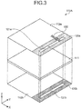
- FIG. 3 is an exploded perspective view for explaining a configuration of an interposer 110A of the wireless device 100A according to the first arrangement.
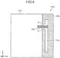
- FIG. 4 is a planar view of the interposer 110A when viewed from the Z-axis direction illustrated in the drawings.
- a semiconductor chip 101 is mounted on the interposer 110A and is sealed using a sealing resin 102.
- the wireless device 100A having such a configuration is referred to as a semiconductor package or a semiconductor module.
- the interposer 110A is a multilayered substrate including an insulating base material 111 and a plurality of conductor layers (in the first arrangement, two conductor layers 112a and 112b).
- the conductor layers 112a and 112b in the interposer 110A are disposed at least at a side of the component installation surface on which components such as the semiconductor chip 101 are installed, and at a side of the reverse surface that is opposite to the component mounting surface.
- the wiring pattern and ground pattern of the interposer 110A are disposed using a metal such as copper.
- the interposer 110A functions as a linking member for connecting the components, such as the semiconductor chip 101, mounted thereon to a larger circuit board on which the wireless device 100A is mounted.
- FIG. 3 is illustrated an example of the interposer 110A in which the conductor layers 112a and 112b are disposed on the principal surface portions at the front and rear sides of the insulating base material 111.
- a state is illustrated in which the insulating base material 111 and the two conductor layers 112a and 112b are virtually separated from each other.
- the two conductor layers are symmetrically positioned with respect to the center in the thickness direction of the interposer 110A.
- one conductor layer is referred to as a first conductor layer 112a and the other conductor layer is referred to as a second conductor layer 112b.
- antenna conductor patterns 120a and 120b are formed in the first conductor layer 112a and the second conductor layer 112b of the interposer 110A; and the antenna conductor patterns 120a and 120b respectively include openings (slits) 121a and 121b functioning as a slot antenna.
- the antenna conductor pattern 120a formed in the first conductor layer 112a is referred to as a first antenna conductor pattern 120a
- the antenna conductor pattern 120b formed in the second conductor layer 112b is referred to as a second antenna conductor pattern 120b.
- the opening 121a of the first antenna conductor pattern 120a is referred to as a first opening 121a
- the opening 121b of the second antenna conductor pattern 120b is referred to as a second opening 121b.
- the detailed explanation of all these constituent elements is given later.
- the semiconductor chip 101 has a metallic pattern of copper, aluminum, or gold formed on the inside or on the surface layer of a semiconductor substrate made of a material such as silicon, silicon germanium, or gallium arsenide; and has an built-in transceiver circuit for transmitting and receiving signals.
- the semiconductor chip 101 is mounted on the component mounting surface of the interposer 110A; and is electrically connected to the wiring pattern and the ground pattern of the interposer 110A via a bonding wire or a bump.
- the semiconductor chip 101 can be configured using a dielectric substrate, a magnetic substrate, a metal, or a combination thereof. Still alternatively, the semiconductor chip 101 can be configured as a chip size package (CSP). Meanwhile, in FIGS. 1 and 2 , although it is illustrated that a single semiconductor chip 101 is mounted on the interposer 110A, it is also possible to have a plurality of semiconductor chips 101 mounted on the interposer 110A. In that case, the semiconductor chips 101 either can be stacked or can be horizontally arranged. Moreover, in FIGS.
- CSP chip size package
- the sealing resin 102 is made of, for example, a thermosetting molding compound having epoxy resin as the base with silica filler added thereto; and is placed on the component mounting surface of the interposer 110A for the purpose of protecting the semiconductor chip 101, and thus seals the semiconductor chip 101.
- the sealing resin 102 is an example of a non-conductor used for sealing the semiconductor chip 101.
- the non-conductor is not limited to resin, and some other non-conductive material or insulating material can alternatively be used.
- the first antenna conductor pattern 120a and the second antenna conductor pattern 120b are formed to have the substantially same shape in such areas (hereinafter, called antenna areas) in the first conductor layer 112a and the second conductor layer 112b, respectively, which are predetermined for placing a slot antenna.
- antenna areas areas in the first conductor layer 112a and the second conductor layer 112b, respectively.
- the first antenna conductor pattern 120a and the second antenna conductor pattern 120b are rectangular in shape, they can be polygonal in shape or can have a complex shape including curved lines in some portion.
- the first opening 121a and the second opening 121b are respectively formed in the first antenna conductor pattern 120a and the second antenna conductor pattern 120b, thereby constituting a slot antenna.
- the length in the longitudinal direction is substantially equal to the half wavelength of the desired frequency used for communication by the wireless device 100A.
- first opening 121a and the second opening 121b are rectangular in shape, they can be of the L shape, the horseshoe shape, the meander shape, or some other complex shape according to the usable frequency, the desired radiation direction, and the shape of the antenna areas.
- the antenna feeder 130, the first antenna conductor pattern 120a, and the second antenna conductor pattern 120b constitute a grounded coplanar line in which the first antenna conductor pattern 120a serves as side ground and the second antenna conductor pattern 120b serves as rear ground. Since the antenna feeder 130 feeds power to the first opening 121a; as illustrated in FIG. 4 , the antenna feeder 130 extends in an intersecting manner with the first opening 121a and has the leading end thereof connected to the first antenna conductor pattern 120a. Moreover, regarding the remaining portion other than the leading end of the antenna feeder 130, gaps G are maintained in order to insulate the antenna feeder 130 from the first antenna conductor pattern 120a. Meanwhile, in FIGS. 3 and 4 , although the base end side of the antenna feeder 130 is not illustrated, it is connected to an RF input-output of the semiconductor chip 101 via a bump or a bonding wire.
- the metal coverage rates of the first conductor layer 112a and the second conductor layer 112b need to be maintained at a comparable level.
- a widely-used countermeasure is to arrange, in a mesh-like shape or a land array shape, a dummy conductor pattern not having electrical functions, so as to maintain the metal coverage rates among different conductor layers at a comparable level.
- a slot antenna is formed as an opening of a conductor pattern within an antenna area. Consequently, the conductor pattern requires a relatively large area, and the metal coverage rates among different conductor layers easily become different.
- the first antenna conductor pattern 120a which is disposed in the first conductor layer 112a of the interposer 110A, has the substantially same shape as the second antenna conductor pattern 120b, which is disposed in the second conductor layer 112b of the interposer 110A.
- the first opening 121a of the first antenna conductor pattern 120a has the substantially same shape as the second opening 121b of the second antenna conductor pattern 120b.
- the first antenna conductor pattern 120a and the second antenna conductor pattern 120b have the substantially equal area of the conductor portion.
- the first opening 121a of the first antenna conductor pattern 120a and the second opening 121b of the second antenna conductor pattern 120b are formed at the substantially same position in the respective antenna areas. That is, the orthogonal projection of the first opening 121a onto the second conductor layer 112b overlaps with the second opening 121b.
- the first opening 121a and the second opening 121b are seen to be overlapping with each other.
- the first antenna conductor pattern 120a and the second antenna conductor pattern 120b having the abovementioned configuration are arranged in the antenna areas of the first conductor layer 112a and the second conductor layer 112b, respectively, of the interposer 110A.
- the metal coverage rates in the antenna areas of the interposer 110A can be maintained at a comparable level between the first conductor layer 112a and the second conductor layer 112b.
- the stress generated at the interface between the insulating base material 111 and the first conductor layer 112a is cancelled out by the stress generated at the interface between the insulating base material 111 and the second conductor layer 112b, thereby enabling achieving reduction in the warpage of the interposer 110A.
- no dummy conductor pattern is placed within the orthogonal projection of the first opening 121a or the second opening 121b onto another conductor layer, it becomes possible to effectively prevent a situation in which the antenna characteristic of the slot antenna deteriorates due to the effect of such a conductor. In this way, in the wireless device 100A according to the first arrangement, the warpage of the interposer 110A can be effectively reduced while maintaining the antenna characteristic of the slot antenna at an excellent level.
- the metal coverage rates of different conductor layers are also desirable to be at a comparable level.
- the other portion of the interposer 110A other than the antenna areas even if a dummy conductor pattern is disposed, the effect on the antenna characteristic is small.
- the metal coverage rates of different conductor layers can be maintained at a comparable level.
- the wireless device 100A according to the first arrangement described above is configured as, for example, a package or a module having the ball grid array (BGA) structure in which terminals formed by solder balls are disposed on the reverse surface side of the interposer 110A.
- the wireless device 100A can be configured as a package or a module having the land grid array (LGA) structure in which lands disposed at the side of the reverse surface of the interposer 110A are used as terminals.
- LGA land grid array
- FIGS. 1 to 4 although the wireless device 100A is illustrated to have a quadrangular planar shape, the outer shape of the wireless device 100A is not limited to this example, and it is possible to have the wireless device 100A in various shapes.
- the first conductor layer 112a and the second conductor layer 112b respectively have the first antenna conductor pattern 120a and the second antenna conductor pattern 120b disposed therein having the substantially equal area of the conductor portion.
- the orthogonal projection of the first opening 121a, which is formed in the first antenna conductor pattern 120a, onto the second conductor layer 112b overlaps with the second opening 121b formed in the second antenna conductor pattern 120b.
- the metal coverage rates of the first conductor layer 112a and the second conductor layer 112b can be maintained at a comparable level without causing significant deterioration in the antenna characteristic of the slot antenna.
- an excellent antenna characteristic can be achieved along with achieving a decrease in the warpage of the interposer 110A.
- the feeder line to the slot antenna a grounded coplanar line is used that is insusceptible to the external environment. For that reason, at the time of mounting the wireless device 100A, the effect on the antenna characteristic attributed to the environment can be reduced in an effective manner. Moreover, as compared to a microstrip line, the grounded coplanar line enables adjustment of the characteristic impedance over a wide range. Hence, at the time of feeding power to the slot antenna, it becomes easier to achieve impedance matching. Meanwhile, in the first conductor layer 112a, the gaps G with the antenna feeder 130 are maintained.
- the metal coverage rates in the antenna areas of the first conductor layer 112a and the second conductor layer 112b are not strictly same, the difference therebetween is at an ignorable level. For that reason, even in the configuration in which power to the slot antenna is fed using a grounded coplanar line, the warpage of the interposer 110A can be reduced in an effective manner.
- the interposer 110A illustrated in FIGS. 3 and 4 is configured to include two conductor layers.
- a multilayered substrate including three of more layers a plurality of cores, in each of which conductor layers are formed in advance at the front and reverse sides of an insulator, is bonded using prepreg made of an insulator.
- prepreg instead of using prepreg, sometimes a bonding film made of an insulator is also used. In that case, the insulators of the cores along with prepreg or a bonding film correspond to the insulating base material 111 of the interposer 110A.
- FIGS. 5 and 6 are diagrams illustrating an example of the interposer 110A having three conductor layers.
- FIG. 5 is an exploded perspective diagram for explaining a configuration of the concerned interposer 110A.
- FIG. 6 is a planar view of the concerned interposer 110A when viewed from the Z-axis direction illustrated in the drawings.
- a third conductor layer 112c is disposed in between the two insulating base materials 111a and 111b (i.e., disposed at the center in the width direction of the interposer 110A).
- a third antenna conductor pattern 120c is formed that is identical to the first antenna conductor pattern 120a and the second antenna conductor pattern 120b.
- the third antenna conductor pattern 120c has a third opening 121c formed therein that is identical to the first opening 121a and the second opening 121b.
- the antenna feeder 130 is disposed in the third conductor layer 112c.
- the third opening 121c of the third antenna conductor pattern 120c receives coplanar power supply from the antenna feeder 130; the first opening 121a, the second opening 121b, and the third opening 121c function as a slot antenna and become able to radiate or receive electromagnetic waves of the desired frequency in an efficient manner.
- the antenna feeder 130 disposed in the third conductor layer 112c, the first antenna conductor pattern 120a disposed in the first conductor layer 112a, and the second antenna conductor pattern 120b disposed in the second conductor layer 112b constitute a stripline in which the first antenna conductor pattern 120a and the second antenna conductor pattern 120b serve as ground.
- the stripline is insusceptible to the external environment. Hence, if the stripline is used as the feedline for the slot antenna, at the time of mounting the wireless device 100A, the impact of the environment on the antenna characteristic can be reduced in an effective manner.
- the first opening 121a of the first antenna conductor pattern 120a, the second opening 121b of the second antenna conductor pattern 120b, and the third opening 121c of the third antenna conductor pattern 120c are formed at the substantially same position in the respective antenna areas. That is, in the planar view of the interposer 110A when viewed from the direction orthogonal to the principal surface (i.e., when viewed from the Z-axis direction illustrated in the drawings), the first opening 121a, the second opening 121b, and the third opening 121c are seen to be overlapping with each other.
- the metal coverage rates of the first conductor layer 112a and the second conductor layer 112b can be maintained at a comparable level without causing significant deterioration in the antenna characteristic of the slot antenna.
- an excellent antenna characteristic can be achieved along with achieving a decrease in the warpage of the interposer 110A.
- the third antenna conductor pattern 120c is disposed in the third conductor layer 112c.
- the configuration can be such that no antenna conductor pattern is disposed in the third conductor layer 112c.
- the antenna feeder 130 is disposed that performs electromagnetic-field-coupling-type power feeding so as to feed power to the first opening 121a and the second opening 121b functioning as a slot antenna.
- the antenna feeder 130 can alternatively be disposed in the first conductor layer 112a or the second conductor layer 112b. With that, a grounded coplanar line can be configured and coplanar power feeding can be performed.
- the interposer 110A having three conductor layers is illustrated, the interposer 110A having four or more conductor layers can also be configured.
- one conductor layer is referred to as the first conductor layer 112a and the other conductor layer is referred to as the second conductor layer 112b; and the first antenna conductor pattern 120a and the second antenna conductor pattern 120b are formed in the first conductor layer 112a and the second conductor layer 112b, respectively.
- an excellent antenna characteristic can be achieved along with achieving a decrease in the warpage of the interposer 110A.
- the first opening 121a and the second opening 121b have the substantially same shape and are formed at the substantially same position in the respective antenna areas.
- the first opening 121a can be slightly smaller in size than the second opening 121b.
- FIGS. 8 and 9 are diagrams illustrating the interposer 110A according to the second modification.
- FIG. 8 is an exploded perspective view for explaining a configuration of the interposer 110A according to the second modification.
- FIG. 9 is a planar view of the interposer 110A according to the second modification when viewed from the Z-axis direction illustrated in the drawings.
- the first opening 121a of on the first antenna conductor pattern 120a which receives coplanar power supply from the antenna feeder 130, is slightly smaller in size than the second opening 121b of the second antenna conductor pattern 120b. That is, an orthogonal projection P (see FIG. 8 ) of the first opening 121a onto the second conductor layer 112b falls within the second opening 121b.
- the interposer 110A is a multilayered substrate including a plurality of conductor layers, there are cases where misalignment occurs among the conductor layers during manufacturing. Although the misalignment is only small in amount, if the first opening 121a and the second opening 121b have the same size, then the misalignment among the conductor layers causes changes in the antenna characteristic of the slot antenna. That is, in the planar view of the interposer 110A when viewed from the direction orthogonal to the principal surface, the overlapping area between the first opening 121a and the second opening 121b represents the effective dimensions of the slot antenna. However, if the first opening 121a and the second opening 121b have the same size, then the size of the overlapping area changes due to the misalignment among the conductor layers, and the antenna characteristic also undergoes changes.
- the interposer 110A when the first opening 121a is formed to be slightly smaller in size than the second opening 121b, and when the orthogonal projection P of the first opening 121a onto the second conductor layer 112b falls within the second opening 121b; even if there occurs misalignment among the conductor layers during manufacturing of the substrate, the effective dimension of the slot antenna is maintained at the dimension of the first opening 121a.
- the antenna characteristic undergoes changes due to the misalignment among the conductor layers during manufacturing of the substrate.
- the difference in the sizes of the first opening 121a and the second opening 121b can be determined by taking into account the tolerance of the misalignment among the conductor layers during manufacturing of the substrate. Since there is only a slight difference in the sizes of the first opening 121a and the second opening 121b, the metal coverage rates of the first opening 121a and the second opening 121b are maintained at a comparable level.
- the metal coverage rates of the first opening 121a and the second opening 121b are maintained at a comparable level.
- an excellent antenna characteristic can be achieved along with achieving a decrease in the warpage of the interposer 110A.
- the second modification since there is an enhancement in the robustness of the antenna characteristic against the misalignment among the conductor layers, it becomes possible to enhance the yield during the substrate manufacturing process.
- the interposer 110A has a parallel plate structure in which a plurality of conductor patterns is formed. Hence, when the slot antenna radiates or receives electromagnetic waves, there is a possibility of leakage of some electromagnetic waves inside the parallel plate structure.
- the first antenna conductor pattern 120a which is disposed in the first conductor layer 112a
- the second antenna conductor pattern 120b which is disposed in the second conductor layer 112b
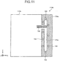
- FIGS. 10 and 11 are diagrams illustrating the interposer 110A according to the third modification.
- FIG. 10 is an exploded perspective view for explaining a configuration of the interposer 110A according to the third modification.
- FIG. 11 is a planar view of the interposer 110A according to the third modification when viewed from the Z-axis direction illustrated in the drawings.
- conductive via holes 150 that electrically connect the first antenna conductor pattern 120a to the second antenna conductor pattern 120b are disposed to penetrate through the insulating base material 111 across the first conductor layer 112a and the second conductor layer 112b.
- the conductive via holes 150 are disposed at the periphery of the first opening 121a and the second opening 121b, and surround the first opening 121a and the second opening 121b.
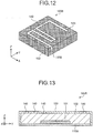
- FIG. 12 is a perspective view illustrating the external appearance of the wireless device 100B according to the second arrangement.
- FIG. 13 is a cross-sectional view of the wireless device 100B according to the second arrangement.
- FIG. 14 is an exploded perspective view for explaining a configuration of an interposer 110B that is installed in the wireless device 100B according to the second arrangement.
- FIG. 15 is a planar view of the interposer 110B when viewed from the Z-axis direction illustrated in the drawings.
- the semiconductor chip 101 that is mounted on the interposer 110B is sealed using the sealing resin 102; and the surfaces of the sealing resin and the side surfaces of the interposer 110B are covered by a conductive film 103.
- the wireless device 100B having such a configuration is called a shielding-function-equipped semiconductor package or a shielding-function-equipped semiconductor module.
- the conductive film 103 is either made of a highly-conductive metal such as copper or silver or made of a conductive paste that is a mixture of a metal such as silver and an insulating material such as epoxy resin; and is formed as a film for covering the surfaces (the outside surfaces) of the sealing resin 102 and the side surfaces of the interposer 110B.
- the whole circumference of the interposer 110B, excluding the reverse surface thereof, is covered by the conductive film 103.
- a surface of the conductive film 103 which is opposite to the component mounting surface of the interposer 110B is called the principal surface portion of the conductive film 103.
- the surfaces of the conductive film 103 which are opposite to the side surfaces of the interposer 110B are called the side surface portions of the conductive film 103.
- the conductive film 103 has a shielding function by which the high-frequency electromagnetic waves (in the range of few tens of MHz to few GHz) that are generated primarily from the semiconductor chip 101 are prevented from leaking in the form of radiation noise to the outside of the wireless device 100B.
- the shielding effectiveness attributed to the conductive film 103 is dependent on the sheet resistance value obtained by dividing the resistivity of the conductive film 103 by the thickness thereof. In order to enable reproducible prevention of the radiation noise leakage, it is desirable that the conductive film 103 has the sheet resistance value to be equal to or smaller than 0.5 ⁇ .
- the conductive film 103 is electrically connected to the first antenna conductor pattern 120a, which is disposed in the first conductor layer 112a of the interposer 110B, and to the second antenna conductor pattern 120b, which is disposed in the second conductor layer 112b of the interposer 110B. That is, since the conductive film 103 covers not only the surfaces of the sealing resin 102 but also the side surfaces of the interposer 110B, it makes contact with the first antenna conductor pattern 120a and the second antenna conductor pattern 120b having ground potential on the side surface of the interposer 110B, and gets electrically connected to the first antenna conductor pattern 120a and the second antenna conductor pattern 120b. As a result of a low-resistance connection of the conductive film 103 to the conductor patterns having ground potential in the interposer 110B, a high shielding effectiveness can be achieved.
- an opening (hereinafter, called a shielding opening) 140 is formed that is continuous with the first opening 121a of the first antenna conductor pattern 120a and the second opening 121b of the second antenna conductor pattern 120b.
- the shielding opening 140, the first opening 121a, and the second opening 121b together function as a single slot antenna. More particularly, for example, as illustrated in FIG. 12 , the shielding opening 140 is formed from the principal surface portion to the side surface portion of the conductive film 103. Moreover, as illustrated in FIG.
- the first opening 121a of the first antenna conductor pattern 120a is formed in such a way that one end 122a thereof reaches the side surface of the interposer 110B; and becomes continuous with the shielding opening 140 formed in the side surface portion of the conductive film 103, at the end 122a.
- the second opening 121b of the second antenna conductor pattern 120b is formed in such a way that one end 122b thereof reaches the side surface of the interposer 110B; and becomes continuous with the shielding opening 140 formed in the side surface portion of the conductive film 103, at the end 122b.
- the first opening 121a is formed as a cut (slit) taken from the side surface of the interposer 110B onto the first antenna conductor pattern 120a that is disposed adjacent to the side surface of the interposer 110B.
- the second opening 121b is formed as a cut (slit) taken from the side surface of the interposer 110B onto the second antenna conductor pattern 120b that is disposed adjacent to the side surface of the interposer 110B.
- the first antenna conductor pattern 120a disposed in the first conductor layer 112a of the interposer 110B has the substantially same shape as the second antenna conductor pattern 120b disposed in the second conductor layer 112b of the interposer 110B.
- the first opening 121a of the first antenna conductor pattern 120a has the substantially same shape as the second opening 121b of the second antenna conductor pattern 120b.
- the first antenna conductor pattern 120a and the second antenna conductor pattern 120b have the substantially equal space of the conductor portion.
- the first opening 121a of the first antenna conductor pattern 120a and the second opening 121b of the second antenna conductor pattern 120b are formed at the substantially same position in the respective antenna areas. That is, the orthogonal projection of the first opening 121a onto the second conductor layer 112b overlaps with the second opening 121b.
- the first opening 121a and the second opening 121b are seen to be overlapping with each other.
- the shielding opening 140 is formed by performing cutting work with respect to the principal surface portion and the side surface portion of the conductive film 103 using, for example, a laser beam machine or an end mill machining device. At that time, the shielding opening 140 is formed in the conductive film 103 in alignment with the first opening 121a, which is formed on the first antenna conductor pattern 120a, and with the second opening 121b, which is formed on the second antenna conductor pattern 120b, so that the shielding opening 140 becomes continuous with the first opening 121a and the second opening 121b.
- the first opening 121a formed on the first antenna conductor pattern 120a, the second opening 121b formed on the second antenna conductor pattern 120b, and the shielding opening 140 formed on the conductive film 103 become continuous with each other; the first opening 121a, the second opening 121b, and the shielding opening 140 constitute a single continuous opening.
- the single opening constituted by the first opening 121a, the second opening 121b, and the shielding opening 140 has the length to be substantially equal to the half wavelength of the desired frequency used for communication by the wireless device 100B.
- the first opening 121a or the second opening 121b receives coplanar power supply from the antenna feeder 130
- the single opening constituted by the first opening 121a, the second opening 121b, and the shielding opening 140 functions as a slot antenna and becomes able to radiate or receive electromagnetic waves of the desired frequency in an efficient manner.
- the antenna feeder 130, the first antenna conductor pattern 120a, and the second antenna conductor pattern 120b constitute a grounded coplanar line in which the first antenna conductor pattern 120a serves as side ground and the second antenna conductor pattern 120b serves as rear ground. Since the antenna feeder 130 feeds power to the first opening 121a; as illustrated in FIG. 15 , the antenna feeder 130 extends in an intersecting manner with the first opening 121a and has the leading end thereof connected to the first antenna conductor pattern 120a. Moreover, regarding the remaining portion other than the leading end of the antenna feeder 130, the gaps G are maintained in order to insulate the antenna feeder 130 from the first antenna conductor pattern 120a. Meanwhile, in FIGS. 14 and 15 , although the base end side of the antenna feeder 130 is not illustrated, it is connected to the RF input-output of the semiconductor chip 101 via a bump or a bonding wire.
- the first opening 121a and the second opening 121b, which are formed on the interposer 110B, and the shielding opening 140, which is formed on the conductive film 103, become continuous with each other and constitute a single slot antenna. That makes it easier to secure the length of the slot antenna.
- a slot antenna having the length to be substantially equal to the half wavelength of the desired frequency can be formed in an appropriate manner.
- the slot antenna is used as the radiating element, as compared to a case in which the radiating element is configured using a conductor, an excellent antenna characteristic can be achieved while minimizing the opening area on the conductive film 103; and any degradation in the shielding performance attributed to the formation of an opening in the conductive film 103, which fulfils the role of a shield, can be held down to the minimum.
- the first conductor layer 112a and the second conductor layer 112b of the interposer 110B respectively have the first antenna conductor pattern 120a and the second antenna conductor pattern 120b disposed therein having the substantially equal area of the conductor portion.
- the orthogonal projection of the first opening 121a, which is formed in the first antenna conductor pattern 120a, onto the second conductor layer 112b overlaps with the second opening 121b formed in the second antenna conductor pattern 120b.
- the metal coverage rates of the first conductor layer 112a and the second conductor layer 112b of the interposer 110B can be maintained at a comparable level without causing significant deterioration in the antenna characteristic of the slot antenna.
- an excellent antenna characteristic can be achieved along with achieving a decrease in the warpage of the interposer 110B.
- the interposer 110B If warpage occurs in the interposer 110B, not only it becomes difficult to perform singulation (dicing) of the interposer 110B, but it also becomes difficult to perform the processing for forming the shielding opening 140 in the conductive film 103, and the shielding opening 140 becomes susceptible to misalignment. As a result, the first opening 121a and the second opening 121b, which are formed in the interposer 110B, become non-continuous with the shielding opening 140, and may not function as a shielding antenna. In contrast, in the wireless device 100B according to the second arrangement, since the warpage of the interposer 110B gets reduced, the unfavorable situation explained above can be effectively prevented and a sophisticated wireless device 100B can be achieved.
- the interposer 110B having three or more conductor layers can be used.
- the configuration can be such that the orthogonal projection P (see FIG. 8 ) of the first opening 121a, which is formed in the interposer 110B, onto the second conductor layer 112b falls within the second opening 121b.
- the first antenna conductor pattern 120a which is formed in the first conductor layer 112a of the interposer 110B
- the second antenna conductor pattern 120b which is formed in the second conductor layer 112b of the interposer 110B, can be electrically connected using the conductive via holes 150.
- the warpage of the interposer can be held down in an effective manner.
Landscapes
- Engineering & Computer Science (AREA)
- Microelectronics & Electronic Packaging (AREA)
- Details Of Aerials (AREA)
- Waveguide Aerials (AREA)
Abstract
According to an arrangement, a wireless device (100A; 100B) includes an interposer (110A; 110B) including conductor layers (112a, 112b); a semiconductor chip (101) mounted on the interposer (110A; 110B) and including a built-in transceiver circuit; and a non-conductor (102) placed on the interposer (110A; 110B) and sealing the semiconductor chip (101). From among the conductor layers (112a, 112b), a first conductor layer (112a) and a second conductor layer (112b) are symmetrically positioned with respect to center in a thickness direction of the interposer (110A; 110B) and respectively have a first antenna conductor pattern (120a) and a second antenna conductor pattern (120b). The first antenna conductor pattern (120a) and the second antenna conductor pattern (120b) respectively have a first opening (121a) and a second opening (121b) functioning as a slot antenna. An orthogonal projection of the first opening (121a) onto the second conductor layer (112b) overlaps with the second opening (121b).
Description
- The present disclosure relates to a wireless device.
- Conventionally, a method is known for having a slot antenna built into a semiconductor package in which a semiconductor chip is mounted on an interposer. Moreover, in order to add a shielding function to the semiconductor package, a technique for implementing a module with a built-in antenna has been proposed in which the surface of an sealing resin for sealing the semiconductor chip is covered using a conductive film; an opening is formed that extends from the conductive film for shielding to a conductive layer of the interposer; and the opening is made to function as a slot antenna.
- A slot antenna of the interposer is formed as an opening in a conductor pattern of a conductor layer. Since the shape of the conductor pattern is such that the opening is included therein, it becomes necessary to secure a relatively large space. In the case of forming a slot antenna in an interposer having a plurality of conductor layers, in the areas in which the slot antenna is to be formed, there occur differences in the metal coverage rates of the conductor layers thereby making the interposer susceptible to warpage. Particularly, an interposer is manufactured by arranging a number of interposers on a single substrate. Thus, the warpage occurring in the individual interposers gets accumulated, and the entire interposer tends to have a large warpage. For that reason, there are times when defects occur during the reflow process for mounting components on the interposer, during the resin sealing process or the dicing process in the semiconductor package manufacturing, and the reflow process for mounting the semiconductor package on the mounting interposer. Hence, there has been a demand for effectively reducing the warpage of the interposer.
-
-
FIG. 1 is a perspective view of a wireless device according to a first arrangement; -
FIG. 2 is a cross-sectional view of the wireless device according to the first arrangement; -
FIG. 3 is an exploded perspective view for explaining a configuration of an interposer; -
FIG. 4 is a planar view of the interposer; -
FIG. 5 is an exploded perspective view for explaining a configuration of the interposer; -
FIG. 6 is a planar view of the interposer; -
FIG. 7 is an exploded perspective view for explaining a configuration of the interposer; -
FIG. 8 is an exploded perspective view for explaining a configuration of the interposer; -
FIG. 9 is a planar view of the interposer; -
FIG. 10 is an exploded perspective view for explaining a configuration of the interposer; -
FIG. 11 is a planar view of the interposer; -
FIG. 12 is a perspective view of a wireless device according to a second arrangement; -
FIG. 13 is a cross-sectional view of the wireless device according to the second arrangement; -
FIG. 14 is an exploded perspective view for explaining a configuration of an interposer; and -
FIG. 15 is a planar view of the interposer. - According to an arrangement, a wireless device includes an interposer, a semiconductor chip, and a non-conductor. The interposer comprises a plurality of conductor layers.
The semiconductor chip is mounted on the interposer and includes a built-in transceiver circuit. The non-conductor is placed on the interposer and seals the semiconductor chip. From among the plurality of conductor layers of the interposer, a first conductor layer and a second conductor layer are symmetrically positioned with respect to center in a thickness direction of the interposer. The first conductor layer has a first antenna conductor pattern disposed herein and the second conductor layer has a second antenna conductor pattern disposed therein. The first antenna conductor pattern and the second antenna conductor pattern have substantially equal area. The first antenna conductor pattern has a first opening formed therein and the second antenna conductor pattern has a second opening formed therein. The first opening and the second opening function as a slot antenna. An orthogonal projection of the first opening onto the second conductor layer overlaps with the second opening. - Arrangements of a wireless device are described below in detail with reference to the accompanying drawings. In the following explanation, the constituent elements having identical functions are referred to by the same reference numerals, and the redundant explanation is not repeated.
- Firstly, explained below with reference to
FIGS. 1 to 4 is awireless device 100A according to a first arrangement.FIG. 1 is a perspective view of the external appearance of thewireless device 100A according to the first arrangement.FIG. 2 is a cross-sectional view of thewireless device 100A according to the first arrangement.FIG. 3 is an exploded perspective view for explaining a configuration of aninterposer 110A of thewireless device 100A according to the first arrangement.FIG. 4 is a planar view of theinterposer 110A when viewed from the Z-axis direction illustrated in the drawings. - As illustrated in
FIGS. 1 and 2 , in thewireless device 100A according to the first arrangement, asemiconductor chip 101 is mounted on theinterposer 110A and is sealed using asealing resin 102. Thewireless device 100A having such a configuration is referred to as a semiconductor package or a semiconductor module. - As illustrated in
FIG. 3 , theinterposer 110A is a multilayered substrate including aninsulating base material 111 and a plurality of conductor layers (in the first arrangement, twoconductor layers conductor layers interposer 110A are disposed at least at a side of the component installation surface on which components such as thesemiconductor chip 101 are installed, and at a side of the reverse surface that is opposite to the component mounting surface. In theconductor layers interposer 110A are disposed using a metal such as copper. Theinterposer 110A functions as a linking member for connecting the components, such as thesemiconductor chip 101, mounted thereon to a larger circuit board on which thewireless device 100A is mounted. - In
FIG. 3 is illustrated an example of theinterposer 110A in which theconductor layers insulating base material 111. In order to make the structure easy to understand, a state is illustrated in which theinsulating base material 111 and the twoconductor layers interposer 110A. Of the twoconductor layers first conductor layer 112a and the other conductor layer is referred to as asecond conductor layer 112b. - In the
wireless device 100A according to the first arrangement, in thefirst conductor layer 112a and thesecond conductor layer 112b of theinterposer 110A,antenna conductor patterns antenna conductor patterns antenna conductor pattern 120a formed in thefirst conductor layer 112a is referred to as a firstantenna conductor pattern 120a, and theantenna conductor pattern 120b formed in thesecond conductor layer 112b is referred to as a secondantenna conductor pattern 120b. Moreover, the opening 121a of the firstantenna conductor pattern 120a is referred to as a first opening 121a, and the opening 121b of the secondantenna conductor pattern 120b is referred to as a second opening 121b. The detailed explanation of all these constituent elements is given later. - The
semiconductor chip 101 has a metallic pattern of copper, aluminum, or gold formed on the inside or on the surface layer of a semiconductor substrate made of a material such as silicon, silicon germanium, or gallium arsenide; and has an built-in transceiver circuit for transmitting and receiving signals. Thesemiconductor chip 101 is mounted on the component mounting surface of theinterposer 110A; and is electrically connected to the wiring pattern and the ground pattern of theinterposer 110A via a bonding wire or a bump. - Alternatively, the
semiconductor chip 101 can be configured using a dielectric substrate, a magnetic substrate, a metal, or a combination thereof. Still alternatively, thesemiconductor chip 101 can be configured as a chip size package (CSP). Meanwhile, inFIGS. 1 and 2 , although it is illustrated that asingle semiconductor chip 101 is mounted on theinterposer 110A, it is also possible to have a plurality ofsemiconductor chips 101 mounted on theinterposer 110A. In that case, thesemiconductor chips 101 either can be stacked or can be horizontally arranged. Moreover, inFIGS. 1 and 2 , although only thesemiconductor chip 101 is illustrated to have been mounted on theinterposer 110A, other components such as a chip capacitor, a resistance, an inductor, and an integrated circuit (IC) can also be mounted on theinterposer 110A in addition to thesemiconductor chip 101. - The sealing
resin 102 is made of, for example, a thermosetting molding compound having epoxy resin as the base with silica filler added thereto; and is placed on the component mounting surface of theinterposer 110A for the purpose of protecting thesemiconductor chip 101, and thus seals thesemiconductor chip 101. Herein, the sealingresin 102 is an example of a non-conductor used for sealing thesemiconductor chip 101. However, the non-conductor is not limited to resin, and some other non-conductive material or insulating material can alternatively be used. - As illustrated in
FIG. 3 , the firstantenna conductor pattern 120a and the secondantenna conductor pattern 120b are formed to have the substantially same shape in such areas (hereinafter, called antenna areas) in thefirst conductor layer 112a and thesecond conductor layer 112b, respectively, which are predetermined for placing a slot antenna. In the example illustrated inFIG. 3 , although the firstantenna conductor pattern 120a and the secondantenna conductor pattern 120b are rectangular in shape, they can be polygonal in shape or can have a complex shape including curved lines in some portion. - In the
wireless device 100A according to the first arrangement, thefirst opening 121a and thesecond opening 121b are respectively formed in the firstantenna conductor pattern 120a and the secondantenna conductor pattern 120b, thereby constituting a slot antenna. Regarding thefirst opening 121a and thesecond opening 121b, the length in the longitudinal direction is substantially equal to the half wavelength of the desired frequency used for communication by thewireless device 100A. When at least either thefirst opening 121a or thesecond opening 121b (in the example illustrated inFIG. 3 , thefirst opening 121a) receives coplanar power supply from anantenna feeder 130, thefirst opening 121a and thesecond opening 121b function as a slot antenna and become able to radiate or receive electromagnetic waves of the desired frequency in an efficient manner. In the example illustrated inFIG. 3 , although thefirst opening 121a and thesecond opening 121b are rectangular in shape, they can be of the L shape, the horseshoe shape, the meander shape, or some other complex shape according to the usable frequency, the desired radiation direction, and the shape of the antenna areas. - The
antenna feeder 130, the firstantenna conductor pattern 120a, and the secondantenna conductor pattern 120b constitute a grounded coplanar line in which the firstantenna conductor pattern 120a serves as side ground and the secondantenna conductor pattern 120b serves as rear ground. Since theantenna feeder 130 feeds power to thefirst opening 121a; as illustrated inFIG. 4 , theantenna feeder 130 extends in an intersecting manner with thefirst opening 121a and has the leading end thereof connected to the firstantenna conductor pattern 120a. Moreover, regarding the remaining portion other than the leading end of theantenna feeder 130, gaps G are maintained in order to insulate theantenna feeder 130 from the firstantenna conductor pattern 120a. Meanwhile, inFIGS. 3 and4 , although the base end side of theantenna feeder 130 is not illustrated, it is connected to an RF input-output of thesemiconductor chip 101 via a bump or a bonding wire. - In order to reduce the warpage of the
interposer 110A, the metal coverage rates of thefirst conductor layer 112a and thesecond conductor layer 112b need to be maintained at a comparable level. However, for convenience of placement of the signal wiring and the ground pattern, there are cases where the metal coverage rates differ among different conductor layers. In such a case, a widely-used countermeasure is to arrange, in a mesh-like shape or a land array shape, a dummy conductor pattern not having electrical functions, so as to maintain the metal coverage rates among different conductor layers at a comparable level. - However, in the case of arranging a dummy pattern in an antenna area of the interposer 110A, since the dummy pattern has an adverse impact on the antenna characteristic, there are limitations on the arrangement of the dummy pattern. That is, generally, a slot antenna is formed as an opening of a conductor pattern within an antenna area. Consequently, the conductor pattern requires a relatively large area, and the metal coverage rates among different conductor layers easily become different. When a dummy pattern is arranged in an antenna area with the aim of holding down the differences in the metal coverage rates of different conductor layers, if the dummy conductor pattern is placed within the area of orthogonal projection from an opening, which functions as a slot antenna, onto another conductor layer; then the antenna characteristic of the slot antenna deteriorates in a significant way. On the other hand, with the aim of ensuring that the antenna characteristic of the slot antenna does not deteriorate, if a restriction is applied for not placing a dummy pattern within the area of orthogonal projection from the opening functioning as a slot antenna onto another conductor layer, then the differences in the metal coverage rates of different conductor layers in the antenna areas still remain in spite of adjusting the metal coverage rates by placing the dummy pattern.
- In contrast, in the
wireless device 100A according to the first arrangement, the firstantenna conductor pattern 120a, which is disposed in thefirst conductor layer 112a of theinterposer 110A, has the substantially same shape as the secondantenna conductor pattern 120b, which is disposed in thesecond conductor layer 112b of theinterposer 110A. Moreover, thefirst opening 121a of the firstantenna conductor pattern 120a has the substantially same shape as thesecond opening 121b of the secondantenna conductor pattern 120b. Hence, the firstantenna conductor pattern 120a and the secondantenna conductor pattern 120b have the substantially equal area of the conductor portion. - Furthermore, the
first opening 121a of the firstantenna conductor pattern 120a and thesecond opening 121b of the secondantenna conductor pattern 120b are formed at the substantially same position in the respective antenna areas. That is, the orthogonal projection of thefirst opening 121a onto thesecond conductor layer 112b overlaps with thesecond opening 121b. In other words, in the planar view of theinterposer 110A when viewed from the direction orthogonal to the principal surface (i.e., when viewed from the Z-axis direction illustrated in the drawings), thefirst opening 121a and thesecond opening 121b are seen to be overlapping with each other. - In the
wireless device 100A according to the first arrangement, the firstantenna conductor pattern 120a and the secondantenna conductor pattern 120b having the abovementioned configuration are arranged in the antenna areas of thefirst conductor layer 112a and thesecond conductor layer 112b, respectively, of theinterposer 110A. As a result, the metal coverage rates in the antenna areas of theinterposer 110A can be maintained at a comparable level between thefirst conductor layer 112a and thesecond conductor layer 112b. As a result, the stress generated at the interface between the insulatingbase material 111 and thefirst conductor layer 112a is cancelled out by the stress generated at the interface between the insulatingbase material 111 and thesecond conductor layer 112b, thereby enabling achieving reduction in the warpage of theinterposer 110A. Moreover, since no dummy conductor pattern is placed within the orthogonal projection of thefirst opening 121a or thesecond opening 121b onto another conductor layer, it becomes possible to effectively prevent a situation in which the antenna characteristic of the slot antenna deteriorates due to the effect of such a conductor. In this way, in thewireless device 100A according to the first arrangement, the warpage of theinterposer 110A can be effectively reduced while maintaining the antenna characteristic of the slot antenna at an excellent level. - Meanwhile, in order to reduce the warpage of the
interposer 110A, regarding the other portion of theinterposer 110A other than the antenna areas, it is also desirable to have the metal coverage rates of different conductor layers to be at a comparable level. In the other portion of theinterposer 110A other than the antenna areas, even if a dummy conductor pattern is disposed, the effect on the antenna characteristic is small. Hence, by placing a dummy pattern according to the conventional method, the metal coverage rates of different conductor layers can be maintained at a comparable level. - The
wireless device 100A according to the first arrangement described above is configured as, for example, a package or a module having the ball grid array (BGA) structure in which terminals formed by solder balls are disposed on the reverse surface side of theinterposer 110A. Alternatively, without disposing the terminals formed by solder balls, thewireless device 100A can be configured as a package or a module having the land grid array (LGA) structure in which lands disposed at the side of the reverse surface of theinterposer 110A are used as terminals. Meanwhile, inFIGS. 1 to 4 , although thewireless device 100A is illustrated to have a quadrangular planar shape, the outer shape of thewireless device 100A is not limited to this example, and it is possible to have thewireless device 100A in various shapes. - As described above, in the
wireless device 100A according to the first arrangement, in the antenna areas of theinterposer 110A, thefirst conductor layer 112a and thesecond conductor layer 112b respectively have the firstantenna conductor pattern 120a and the secondantenna conductor pattern 120b disposed therein having the substantially equal area of the conductor portion. Moreover, the orthogonal projection of thefirst opening 121a, which is formed in the firstantenna conductor pattern 120a, onto thesecond conductor layer 112b overlaps with thesecond opening 121b formed in the secondantenna conductor pattern 120b. Hence, according to the first arrangement, the metal coverage rates of thefirst conductor layer 112a and thesecond conductor layer 112b can be maintained at a comparable level without causing significant deterioration in the antenna characteristic of the slot antenna. As a result, an excellent antenna characteristic can be achieved along with achieving a decrease in the warpage of theinterposer 110A. - Moreover, in the first arrangement, as the feeder line to the slot antenna, a grounded coplanar line is used that is insusceptible to the external environment. For that reason, at the time of mounting the
wireless device 100A, the effect on the antenna characteristic attributed to the environment can be reduced in an effective manner. Moreover, as compared to a microstrip line, the grounded coplanar line enables adjustment of the characteristic impedance over a wide range. Hence, at the time of feeding power to the slot antenna, it becomes easier to achieve impedance matching. Meanwhile, in thefirst conductor layer 112a, the gaps G with theantenna feeder 130 are maintained. Hence, although the metal coverage rates in the antenna areas of thefirst conductor layer 112a and thesecond conductor layer 112b are not strictly same, the difference therebetween is at an ignorable level. For that reason, even in the configuration in which power to the slot antenna is fed using a grounded coplanar line, the warpage of theinterposer 110A can be reduced in an effective manner. - The
interposer 110A illustrated inFIGS. 3 and4 is configured to include two conductor layers. Alternatively, it is also possible to configure theinterposer 110A to include three or more conductor layers and include two or more insulating base materials placed in between the conductor layers. Generally, in a multilayered substrate including three of more layers; a plurality of cores, in each of which conductor layers are formed in advance at the front and reverse sides of an insulator, is bonded using prepreg made of an insulator. Moreover, instead of using prepreg, sometimes a bonding film made of an insulator is also used. In that case, the insulators of the cores along with prepreg or a bonding film correspond to the insulatingbase material 111 of theinterposer 110A. -
FIGS. 5 and6 are diagrams illustrating an example of theinterposer 110A having three conductor layers.FIG. 5 is an exploded perspective diagram for explaining a configuration of theconcerned interposer 110A.FIG. 6 is a planar view of theconcerned interposer 110A when viewed from the Z-axis direction illustrated in the drawings. - As illustrated in
FIG. 5 , in theinterposer 110A according to the first modification, two insulatingbase materials first conductor layer 112a and thesecond conductor layer 112b; and athird conductor layer 112c is disposed in between the two insulatingbase materials interposer 110A). Moreover, in the antenna area of thethird conductor layer 112c, a thirdantenna conductor pattern 120c is formed that is identical to the firstantenna conductor pattern 120a and the secondantenna conductor pattern 120b. The thirdantenna conductor pattern 120c has athird opening 121c formed therein that is identical to thefirst opening 121a and thesecond opening 121b. - Furthermore, in the
interposer 110A according to the first modification, theantenna feeder 130 is disposed in thethird conductor layer 112c. When thethird opening 121c of the thirdantenna conductor pattern 120c receives coplanar power supply from theantenna feeder 130; thefirst opening 121a, thesecond opening 121b, and thethird opening 121c function as a slot antenna and become able to radiate or receive electromagnetic waves of the desired frequency in an efficient manner. - The
antenna feeder 130 disposed in thethird conductor layer 112c, the firstantenna conductor pattern 120a disposed in thefirst conductor layer 112a, and the secondantenna conductor pattern 120b disposed in thesecond conductor layer 112b constitute a stripline in which the firstantenna conductor pattern 120a and the secondantenna conductor pattern 120b serve as ground. In an identical manner to the grounded coplanar line explained earlier, the stripline is insusceptible to the external environment. Hence, if the stripline is used as the feedline for the slot antenna, at the time of mounting thewireless device 100A, the impact of the environment on the antenna characteristic can be reduced in an effective manner. - In the
interposer 110A according to the first modification; thefirst opening 121a of the firstantenna conductor pattern 120a, thesecond opening 121b of the secondantenna conductor pattern 120b, and thethird opening 121c of the thirdantenna conductor pattern 120c are formed at the substantially same position in the respective antenna areas. That is, in the planar view of theinterposer 110A when viewed from the direction orthogonal to the principal surface (i.e., when viewed from the Z-axis direction illustrated in the drawings), thefirst opening 121a, thesecond opening 121b, and thethird opening 121c are seen to be overlapping with each other. - Thus, even in the case of using the
interposer 110A according to the first modification instead of using theinterposer 110A described earlier, the metal coverage rates of thefirst conductor layer 112a and thesecond conductor layer 112b can be maintained at a comparable level without causing significant deterioration in the antenna characteristic of the slot antenna. As a result, an excellent antenna characteristic can be achieved along with achieving a decrease in the warpage of theinterposer 110A. - In the example explained above, the third
antenna conductor pattern 120c is disposed in thethird conductor layer 112c. Alternatively, as illustrated inFIG. 7 , the configuration can be such that no antenna conductor pattern is disposed in thethird conductor layer 112c. In theinterposer 110A illustrated inFIG. 7 , in thethird conductor layer 112c in which no antenna conductor layer is disposed, theantenna feeder 130 is disposed that performs electromagnetic-field-coupling-type power feeding so as to feed power to thefirst opening 121a and thesecond opening 121b functioning as a slot antenna. Meanwhile, instead of disposing theantenna feeder 130 in thethird conductor layer 112c, theantenna feeder 130 can alternatively be disposed in thefirst conductor layer 112a or thesecond conductor layer 112b. With that, a grounded coplanar line can be configured and coplanar power feeding can be performed. - Meanwhile, although the
interposer 110A having three conductor layers is illustrated, theinterposer 110A having four or more conductor layers can also be configured. In that case too, regarding the two conductor layers that are symmetrically positioned with respect to the center in the thickness direction of the interposer 110A, one conductor layer is referred to as thefirst conductor layer 112a and the other conductor layer is referred to as thesecond conductor layer 112b; and the firstantenna conductor pattern 120a and the secondantenna conductor pattern 120b are formed in thefirst conductor layer 112a and thesecond conductor layer 112b, respectively. With that, an excellent antenna characteristic can be achieved along with achieving a decrease in the warpage of theinterposer 110A. - In the
interposer 110A illustrated inFIGS. 3 and4 , thefirst opening 121a and thesecond opening 121b have the substantially same shape and are formed at the substantially same position in the respective antenna areas. However, in theinterposer 110A, as long as the orthogonal projection of thefirst opening 121a onto thesecond conductor layer 112b overlaps with thesecond opening 121b, thefirst opening 121a can be slightly smaller in size than thesecond opening 121b. -
FIGS. 8 and9 are diagrams illustrating theinterposer 110A according to the second modification.FIG. 8 is an exploded perspective view for explaining a configuration of theinterposer 110A according to the second modification.FIG. 9 is a planar view of theinterposer 110A according to the second modification when viewed from the Z-axis direction illustrated in the drawings. - In the
interposer 110A according to the second modification, as illustrated inFIGS. 8 and9 , thefirst opening 121a of on the firstantenna conductor pattern 120a, which receives coplanar power supply from theantenna feeder 130, is slightly smaller in size than thesecond opening 121b of the secondantenna conductor pattern 120b. That is, an orthogonal projection P (seeFIG. 8 ) of thefirst opening 121a onto thesecond conductor layer 112b falls within thesecond opening 121b. - Since the
interposer 110A is a multilayered substrate including a plurality of conductor layers, there are cases where misalignment occurs among the conductor layers during manufacturing. Although the misalignment is only small in amount, if thefirst opening 121a and thesecond opening 121b have the same size, then the misalignment among the conductor layers causes changes in the antenna characteristic of the slot antenna. That is, in the planar view of theinterposer 110A when viewed from the direction orthogonal to the principal surface, the overlapping area between thefirst opening 121a and thesecond opening 121b represents the effective dimensions of the slot antenna. However, if thefirst opening 121a and thesecond opening 121b have the same size, then the size of the overlapping area changes due to the misalignment among the conductor layers, and the antenna characteristic also undergoes changes. - In contrast, in the
interposer 110A according to the second modification, when thefirst opening 121a is formed to be slightly smaller in size than thesecond opening 121b, and when the orthogonal projection P of thefirst opening 121a onto thesecond conductor layer 112b falls within thesecond opening 121b; even if there occurs misalignment among the conductor layers during manufacturing of the substrate, the effective dimension of the slot antenna is maintained at the dimension of thefirst opening 121a. Thus, it becomes possible to effectively prevent an unfavorable situation in which the antenna characteristic undergoes changes due to the misalignment among the conductor layers during manufacturing of the substrate. Herein, the difference in the sizes of thefirst opening 121a and thesecond opening 121b can be determined by taking into account the tolerance of the misalignment among the conductor layers during manufacturing of the substrate. Since there is only a slight difference in the sizes of thefirst opening 121a and thesecond opening 121b, the metal coverage rates of thefirst opening 121a and thesecond opening 121b are maintained at a comparable level. - As described above, in the second modification too, the metal coverage rates of the
first opening 121a and thesecond opening 121b are maintained at a comparable level. As a result, an excellent antenna characteristic can be achieved along with achieving a decrease in the warpage of theinterposer 110A. Moreover, in the second modification, since there is an enhancement in the robustness of the antenna characteristic against the misalignment among the conductor layers, it becomes possible to enhance the yield during the substrate manufacturing process. - The
interposer 110A has a parallel plate structure in which a plurality of conductor patterns is formed. Hence, when the slot antenna radiates or receives electromagnetic waves, there is a possibility of leakage of some electromagnetic waves inside the parallel plate structure. In theinterposer 110A according to a third modification, the firstantenna conductor pattern 120a, which is disposed in thefirst conductor layer 112a, and the secondantenna conductor pattern 120b, which is disposed in thesecond conductor layer 112b, are electrically connected via conductive via holes; and the leakage of electromagnetic waves is suppressed. -
FIGS. 10 and11 are diagrams illustrating theinterposer 110A according to the third modification.FIG. 10 is an exploded perspective view for explaining a configuration of theinterposer 110A according to the third modification.FIG. 11 is a planar view of theinterposer 110A according to the third modification when viewed from the Z-axis direction illustrated in the drawings. - In the
interposer 110A according to the third modification, as illustrated inFIGS. 10 and11 , conductive viaholes 150 that electrically connect the firstantenna conductor pattern 120a to the secondantenna conductor pattern 120b are disposed to penetrate through the insulatingbase material 111 across thefirst conductor layer 112a and thesecond conductor layer 112b. The conductive viaholes 150 are disposed at the periphery of thefirst opening 121a and thesecond opening 121b, and surround thefirst opening 121a and thesecond opening 121b. With such a configuration, it becomes possible to effectively suppress the leakage of electromagnetic waves in the parallel plate structure, thereby resulting in further enhancement of the antenna characteristic of the slot antenna. Moreover, in the third modification too, since the metal coverage rates of thefirst opening 121a and thesecond opening 121b are maintained at a comparable level, an excellent antenna characteristic can be achieved along with achieving a decrease in the warpage of theinterposer 110A. - Explained below with reference to
FIGS. 12 to 15 is awireless device 100B according to a second arrangement.FIG. 12 is a perspective view illustrating the external appearance of thewireless device 100B according to the second arrangement.FIG. 13 is a cross-sectional view of thewireless device 100B according to the second arrangement.FIG. 14 is an exploded perspective view for explaining a configuration of aninterposer 110B that is installed in thewireless device 100B according to the second arrangement.FIG. 15 is a planar view of theinterposer 110B when viewed from the Z-axis direction illustrated in the drawings. - As illustrated in
FIGS. 12 and 13 , in thewireless device 100B according to the second arrangement, thesemiconductor chip 101 that is mounted on theinterposer 110B is sealed using the sealingresin 102; and the surfaces of the sealing resin and the side surfaces of theinterposer 110B are covered by aconductive film 103. Thewireless device 100B having such a configuration is called a shielding-function-equipped semiconductor package or a shielding-function-equipped semiconductor module. - The
conductive film 103 is either made of a highly-conductive metal such as copper or silver or made of a conductive paste that is a mixture of a metal such as silver and an insulating material such as epoxy resin; and is formed as a film for covering the surfaces (the outside surfaces) of the sealingresin 102 and the side surfaces of theinterposer 110B. Thus, in thewireless device 100B according to the second arrangement, the whole circumference of theinterposer 110B, excluding the reverse surface thereof, is covered by theconductive film 103. In the following explanation, a surface of theconductive film 103 which is opposite to the component mounting surface of theinterposer 110B is called the principal surface portion of theconductive film 103. Moreover, the surfaces of theconductive film 103 which are opposite to the side surfaces of theinterposer 110B are called the side surface portions of theconductive film 103. - The
conductive film 103 has a shielding function by which the high-frequency electromagnetic waves (in the range of few tens of MHz to few GHz) that are generated primarily from thesemiconductor chip 101 are prevented from leaking in the form of radiation noise to the outside of thewireless device 100B. The shielding effectiveness attributed to theconductive film 103 is dependent on the sheet resistance value obtained by dividing the resistivity of theconductive film 103 by the thickness thereof. In order to enable reproducible prevention of the radiation noise leakage, it is desirable that theconductive film 103 has the sheet resistance value to be equal to or smaller than 0.5 Ω. - Moreover, the
conductive film 103 is electrically connected to the firstantenna conductor pattern 120a, which is disposed in thefirst conductor layer 112a of theinterposer 110B, and to the secondantenna conductor pattern 120b, which is disposed in thesecond conductor layer 112b of theinterposer 110B. That is, since theconductive film 103 covers not only the surfaces of the sealingresin 102 but also the side surfaces of theinterposer 110B, it makes contact with the firstantenna conductor pattern 120a and the secondantenna conductor pattern 120b having ground potential on the side surface of theinterposer 110B, and gets electrically connected to the firstantenna conductor pattern 120a and the secondantenna conductor pattern 120b. As a result of a low-resistance connection of theconductive film 103 to the conductor patterns having ground potential in theinterposer 110B, a high shielding effectiveness can be achieved. - In the
conductive film 103, an opening (hereinafter, called a shielding opening) 140 is formed that is continuous with thefirst opening 121a of the firstantenna conductor pattern 120a and thesecond opening 121b of the secondantenna conductor pattern 120b. Theshielding opening 140, thefirst opening 121a, and thesecond opening 121b together function as a single slot antenna. More particularly, for example, as illustrated inFIG. 12 , theshielding opening 140 is formed from the principal surface portion to the side surface portion of theconductive film 103. Moreover, as illustrated inFIG. 14 , thefirst opening 121a of the firstantenna conductor pattern 120a is formed in such a way that oneend 122a thereof reaches the side surface of theinterposer 110B; and becomes continuous with theshielding opening 140 formed in the side surface portion of theconductive film 103, at theend 122a. In an identical manner, thesecond opening 121b of the secondantenna conductor pattern 120b is formed in such a way that oneend 122b thereof reaches the side surface of theinterposer 110B; and becomes continuous with theshielding opening 140 formed in the side surface portion of theconductive film 103, at theend 122b. - For example, at the time of performing patterning of the wiring pattern and ground pattern on the
first conductor layer 112a of theinterposer 110B, thefirst opening 121a is formed as a cut (slit) taken from the side surface of theinterposer 110B onto the firstantenna conductor pattern 120a that is disposed adjacent to the side surface of theinterposer 110B. Similarly, at the time of performing patterning of the wiring pattern and ground pattern on thesecond conductor layer 112b of theinterposer 110B, thesecond opening 121b is formed as a cut (slit) taken from the side surface of theinterposer 110B onto the secondantenna conductor pattern 120b that is disposed adjacent to the side surface of theinterposer 110B. - In the
wireless device 100B according to the second arrangement, in an identical manner to thewireless device 100A according to the first arrangement, the firstantenna conductor pattern 120a disposed in thefirst conductor layer 112a of theinterposer 110B has the substantially same shape as the secondantenna conductor pattern 120b disposed in thesecond conductor layer 112b of theinterposer 110B. Moreover, thefirst opening 121a of the firstantenna conductor pattern 120a has the substantially same shape as thesecond opening 121b of the secondantenna conductor pattern 120b. Hence, the firstantenna conductor pattern 120a and the secondantenna conductor pattern 120b have the substantially equal space of the conductor portion. - Furthermore, the
first opening 121a of the firstantenna conductor pattern 120a and thesecond opening 121b of the secondantenna conductor pattern 120b are formed at the substantially same position in the respective antenna areas. That is, the orthogonal projection of thefirst opening 121a onto thesecond conductor layer 112b overlaps with thesecond opening 121b. In other words, in the planar view of theinterposer 110B when viewed from the direction orthogonal to the principal surface (i.e., when viewed from the Z-axis direction illustrated in the drawings), thefirst opening 121a and thesecond opening 121b are seen to be overlapping with each other. - After the
semiconductor chip 101 is mounted on the component mounting surface of theinterposer 110B and is sealed using the sealingresin 102, and after theconductive film 103 is formed; theshielding opening 140 is formed by performing cutting work with respect to the principal surface portion and the side surface portion of theconductive film 103 using, for example, a laser beam machine or an end mill machining device. At that time, theshielding opening 140 is formed in theconductive film 103 in alignment with thefirst opening 121a, which is formed on the firstantenna conductor pattern 120a, and with thesecond opening 121b, which is formed on the secondantenna conductor pattern 120b, so that theshielding opening 140 becomes continuous with thefirst opening 121a and thesecond opening 121b. - Once the
first opening 121a formed on the firstantenna conductor pattern 120a, thesecond opening 121b formed on the secondantenna conductor pattern 120b, and theshielding opening 140 formed on theconductive film 103 become continuous with each other; thefirst opening 121a, thesecond opening 121b, and theshielding opening 140 constitute a single continuous opening. - The single opening constituted by the
first opening 121a, thesecond opening 121b, and theshielding opening 140 has the length to be substantially equal to the half wavelength of the desired frequency used for communication by thewireless device 100B. When at least either thefirst opening 121a or thesecond opening 121b (in the example illustrated inFIG. 14 , thefirst opening 121a) receives coplanar power supply from theantenna feeder 130, the single opening constituted by thefirst opening 121a, thesecond opening 121b, and the shielding opening 140 functions as a slot antenna and becomes able to radiate or receive electromagnetic waves of the desired frequency in an efficient manner. - In the second arrangement too, in an identical manner to the first arrangement, the
antenna feeder 130, the firstantenna conductor pattern 120a, and the secondantenna conductor pattern 120b constitute a grounded coplanar line in which the firstantenna conductor pattern 120a serves as side ground and the secondantenna conductor pattern 120b serves as rear ground. Since theantenna feeder 130 feeds power to thefirst opening 121a; as illustrated inFIG. 15 , theantenna feeder 130 extends in an intersecting manner with thefirst opening 121a and has the leading end thereof connected to the firstantenna conductor pattern 120a. Moreover, regarding the remaining portion other than the leading end of theantenna feeder 130, the gaps G are maintained in order to insulate theantenna feeder 130 from the firstantenna conductor pattern 120a. Meanwhile, inFIGS. 14 and15 , although the base end side of theantenna feeder 130 is not illustrated, it is connected to the RF input-output of thesemiconductor chip 101 via a bump or a bonding wire. - In the
wireless device 100B according to the second arrangement, thefirst opening 121a and thesecond opening 121b, which are formed on theinterposer 110B, and theshielding opening 140, which is formed on theconductive film 103, become continuous with each other and constitute a single slot antenna. That makes it easier to secure the length of the slot antenna. Hence, for example, even if thewireless device 100B is small in size in regard to the desired frequency used for communication, a slot antenna having the length to be substantially equal to the half wavelength of the desired frequency can be formed in an appropriate manner. Moreover, since the slot antenna is used as the radiating element, as compared to a case in which the radiating element is configured using a conductor, an excellent antenna characteristic can be achieved while minimizing the opening area on theconductive film 103; and any degradation in the shielding performance attributed to the formation of an opening in theconductive film 103, which fulfils the role of a shield, can be held down to the minimum. - Meanwhile, in the second arrangement too, in an identical manner to the first arrangement, the
first conductor layer 112a and thesecond conductor layer 112b of theinterposer 110B respectively have the firstantenna conductor pattern 120a and the secondantenna conductor pattern 120b disposed therein having the substantially equal area of the conductor portion. Moreover, the orthogonal projection of thefirst opening 121a, which is formed in the firstantenna conductor pattern 120a, onto thesecond conductor layer 112b overlaps with thesecond opening 121b formed in the secondantenna conductor pattern 120b. Thus, according to the second arrangement, the metal coverage rates of thefirst conductor layer 112a and thesecond conductor layer 112b of theinterposer 110B can be maintained at a comparable level without causing significant deterioration in the antenna characteristic of the slot antenna. As a result, an excellent antenna characteristic can be achieved along with achieving a decrease in the warpage of theinterposer 110B. - If warpage occurs in the
interposer 110B, not only it becomes difficult to perform singulation (dicing) of theinterposer 110B, but it also becomes difficult to perform the processing for forming theshielding opening 140 in theconductive film 103, and theshielding opening 140 becomes susceptible to misalignment. As a result, thefirst opening 121a and thesecond opening 121b, which are formed in theinterposer 110B, become non-continuous with theshielding opening 140, and may not function as a shielding antenna. In contrast, in thewireless device 100B according to the second arrangement, since the warpage of theinterposer 110B gets reduced, the unfavorable situation explained above can be effectively prevented and asophisticated wireless device 100B can be achieved. - Meanwhile, in an identical manner to the first modification of the first arrangement, in the second arrangement too, the
interposer 110B having three or more conductor layers can be used. Moreover, in an identical manner to the second modification of the first arrangement, in the second arrangement too, the configuration can be such that the orthogonal projection P (seeFIG. 8 ) of thefirst opening 121a, which is formed in theinterposer 110B, onto thesecond conductor layer 112b falls within thesecond opening 121b. Furthermore, in an identical manner to the third modification of the first arrangement, in the second arrangement too, the firstantenna conductor pattern 120a, which is formed in thefirst conductor layer 112a of theinterposer 110B, and the secondantenna conductor pattern 120b, which is formed in thesecond conductor layer 112b of theinterposer 110B, can be electrically connected using the conductive viaholes 150. - According to at least one of the arrangements described above, the warpage of the interposer can be held down in an effective manner.
- While certain arrangements have been described, these arrangements have been presented by way of example only, and are not intended to limit the scope of the claims. Indeed, the novel devices described herein may be embodied in a variety of other forms; furthermore, various omissions, substitutions and changes in the form of the devices described herein may be made.
- Example 1. A wireless device includes an interposer, a semiconductor chip, and a non-conductor. The interposer includes a plurality of conductor layers. The semiconductor chip is mounted on the interposer and includes a built-in transceiver circuit. The non-conductor is placed on the interposer. The non-conductor seals the semiconductor chip. From among the plurality of conductor layers of the interposer, a first conductor layer and a second conductor layer are symmetrically positioned with respect to center in a thickness direction of the interposer. The first conductor layer has a first antenna conductor pattern disposed therein and the second conductor layer has a second antenna conductor pattern disposed therein. The first antenna conductor pattern and the second antenna conductor pattern have substantially equal area. The first antenna conductor pattern has a first opening formed therein and the second antenna conductor pattern has a second opening formed therein. The first opening and the second opening function as a slot antenna. An orthogonal projection of the first opening onto the second conductor layer overlaps with the second opening.
- Example 2. In the wireless device according to Example 1, the orthogonal projection of the first opening onto the second conductor layer is within the second opening.
- Example 3. The wireless device according to Example 1 or 2 further includes a conductive film that covers surfaces of the non-conductor and side surfaces of the interposer, and that is electrically connected to the first antenna conductor pattern and to the second antenna conductor pattern. The conductive film has an opening formed therein that is continuous with the first opening and the second opening, and the opening formed in the conductive film, the first opening, and the second opening function as a single slot antenna.
- Example 4. In the wireless device according to any one of Examples 1 to 3, at least one of the first opening and the second opening receives a coplanar power supply from a feeder disposed either in the first conductor layer or the second conductor layer.
- Example 5. In the wireless device according to any one of Examples 1 to 3, at least one of the first opening and the second opening receives an electromagnetic coupling power supply from a feeder disposed in another conductor layer different from the first conductor layer or the second conductor layer.
- Example 6. In the wireless device according to any one of Examples 1 to 5, conductive via holes are disposed around the first opening and the second opening across the first conductor layer and the second conductor layer, and the first antenna conductor pattern and the second antenna conductor pattern are electrically connected via the conductive via holes.
Claims (6)
- A wireless device (100A; 100B) comprising:an interposer (110A; 110B) comprising a plurality of conductor layers (112a, 112b);a semiconductor chip (101) mounted on the interposer (110A; 110B) and comprising a built-in transceiver circuit; anda non-conductor (102) placed on the interposer (110A; 110B), wherein the non-conductor (102) seals the semiconductor chip (101), whereinfrom among the plurality of conductor layers (112a, 112b) of the interposer (110A; 110B), a first conductor layer (112a) and a second conductor layer (112b) are symmetrically positioned with respect to center in a thickness direction of the interposer (110A; 110B), the first conductor layer (112a) having a first antenna conductor pattern (120a) disposed therein and the second conductor layer (112b) having a second antenna conductor pattern (120b) disposed therein, the first antenna conductor pattern (120a) and the second antenna conductor pattern (120b) having substantially equal area,the first antenna conductor pattern (120a) having a first opening (121a) formed therein and the second antenna conductor pattern (120b) having a second opening (121b) formed therein, the first opening (121a) and the second opening (121b) functioning as a slot antenna, andan orthogonal projection of the first opening (121a) onto the second conductor layer (112b) overlaps with the second opening (121b).
- The wireless device (100A; 100B) according to claim 1, wherein the orthogonal projection of the first opening (121a) onto the second conductor layer (112b) is within the second opening (121b).
- The wireless device (100A; 100B) according to claim 1 or 2, further comprising a conductive film (103) that covers surfaces of the non-conductor (102) and side surfaces of the interposer (110A; 110B), and that is electrically connected to the first antenna conductor pattern (120a) and to the second antenna conductor pattern (120b), wherein
the conductive film (103) has an opening (140) formed therein that is continuous with the first opening (121a) and the second opening (121b), and the opening (140) formed in the conductive film, the first opening
(121a), and the second opening (121b) function as a single slot antenna. - The wireless device (100A; 100B) according to any one of claims 1 to 3, wherein at least one of the first opening (121a) and the second opening (121b) receives a coplanar power supply from a feeder (130) disposed either in the first conductor layer (112a) or the second conductor layer (112b).
- The wireless device (100A; 100B) according to any one of claims 1 to 3, wherein at least one of the first opening (121a) and the second opening (121b) receives an electromagnetic coupling power supply from a feeder (130) disposed in another conductor layer (112c) different from the first conductor layer (112a) or the second conductor layer (112b).
- The wireless device (100A; 100B) according to any one of claims 1 to 5, wherein conductive via holes (150) are disposed around the first opening (121a) and the second opening (121b) across the first conductor layer (112a) and the second conductor layer (112b), and the first antenna conductor pattern (120a) and the second antenna conductor pattern (120b) are electrically connected via the conductive via holes (150).
Applications Claiming Priority (1)
| Application Number | Priority Date | Filing Date | Title |
|---|---|---|---|
| JP2017005986A JP6602324B2 (en) | 2017-01-17 | 2017-01-17 | Wireless device |
Publications (1)
| Publication Number | Publication Date |
|---|---|
| EP3349248A1 true EP3349248A1 (en) | 2018-07-18 |
Family
ID=59686890
Family Applications (1)
| Application Number | Title | Priority Date | Filing Date |
|---|---|---|---|
| EP17187573.5A Withdrawn EP3349248A1 (en) | 2017-01-17 | 2017-08-23 | Wireless device |
Country Status (3)
| Country | Link |
|---|---|
| US (1) | US10439264B2 (en) |
| EP (1) | EP3349248A1 (en) |
| JP (1) | JP6602324B2 (en) |
Families Citing this family (10)
| Publication number | Priority date | Publication date | Assignee | Title |
|---|---|---|---|---|
| JP6602324B2 (en) | 2017-01-17 | 2019-11-06 | 株式会社東芝 | Wireless device |
| JP6602326B2 (en) | 2017-02-06 | 2019-11-06 | 株式会社東芝 | Wireless device |
| JP6776280B2 (en) | 2018-01-10 | 2020-10-28 | 株式会社東芝 | Wireless communication module, printed circuit board, and manufacturing method |
| JP7156815B2 (en) * | 2018-05-02 | 2022-10-19 | ラピスセミコンダクタ株式会社 | Antennas and semiconductor devices |
| JP7039527B2 (en) | 2019-07-12 | 2022-03-22 | 株式会社東芝 | Wireless device and manufacturing method of wireless device |
| KR20220064773A (en) * | 2020-11-12 | 2022-05-19 | 삼성전기주식회사 | Chip antenna |
| CN114076853A (en) * | 2021-10-28 | 2022-02-22 | 南京航空航天大学 | System and method for measuring shielding effectiveness of nonlinear conductive material |
| EP4195404B1 (en) * | 2021-12-10 | 2025-07-16 | Robert Bosch GmbH | Slot antenna in a multi-layered printed circuit board |
| CN117855804A (en) * | 2022-09-30 | 2024-04-09 | Oppo广东移动通信有限公司 | Antenna device and electronic equipment |
| WO2025225553A1 (en) * | 2024-04-25 | 2025-10-30 | Agc株式会社 | Laminate and power supply structure |
Citations (3)
| Publication number | Priority date | Publication date | Assignee | Title |
|---|---|---|---|---|
| JP2007221585A (en) * | 2006-02-17 | 2007-08-30 | Furuno Electric Co Ltd | Antenna and manufacturing method thereof |
| US20090256752A1 (en) * | 2008-04-14 | 2009-10-15 | International Business Machines Corporation | Radio frequency (rf) integrated circuit (ic) packages with integrated aperture-coupled patch antenna(s) in ring and/or offset cavities |
| US20140055939A1 (en) * | 2012-08-24 | 2014-02-27 | Kabushiki Kaisha Toshiba | Wireless device, and information processing apparatus and storage device including the wireless device |
Family Cites Families (28)
| Publication number | Priority date | Publication date | Assignee | Title |
|---|---|---|---|---|
| JPH1092981A (en) | 1996-09-17 | 1998-04-10 | Toshiba Corp | Conductive mold package for semiconductor device |
| US20050035437A1 (en) * | 2002-01-23 | 2005-02-17 | Yoshishige Yoshikawa | Package part and method of manufacturing the part |
| AU2002340506A1 (en) | 2002-11-07 | 2004-06-07 | Fractus, S.A. | Integrated circuit package including miniature antenna |
| JP4064834B2 (en) | 2003-02-05 | 2008-03-19 | 株式会社日本自動車部品総合研究所 | Slot antenna |
| US6982480B2 (en) * | 2003-07-31 | 2006-01-03 | The Boeing Company | Near hermetic packaging of gallium arsenide semiconductor devices and manufacturing method therefor |
| US7444734B2 (en) * | 2003-12-09 | 2008-11-04 | International Business Machines Corporation | Apparatus and methods for constructing antennas using vias as radiating elements formed in a substrate |
| JP4112484B2 (en) * | 2003-12-17 | 2008-07-02 | 株式会社東芝 | Wireless device and semiconductor device |
| US7872605B2 (en) | 2005-03-15 | 2011-01-18 | Fractus, S.A. | Slotted ground-plane used as a slot antenna or used for a PIFA antenna |
| US20070209437A1 (en) * | 2005-10-18 | 2007-09-13 | Seagate Technology Llc | Magnetic MEMS device |
| JP4365365B2 (en) * | 2005-10-31 | 2009-11-18 | シャープ株式会社 | Equipment equipped with wireless device and storage structure of wireless device |
| WO2010058337A1 (en) | 2008-11-19 | 2010-05-27 | Nxp B.V. | Millimetre-wave radio antenna module |
| JP5556072B2 (en) | 2009-01-07 | 2014-07-23 | ソニー株式会社 | Semiconductor device, method of manufacturing the same, and millimeter wave dielectric transmission device |
| FR2945379B1 (en) | 2009-05-05 | 2011-07-22 | United Monolithic Semiconductors Sa | MINIATURE HYPERFREQUENCY COMPONENT FOR SURFACE MOUNTING |
| US20110168784A1 (en) * | 2010-01-14 | 2011-07-14 | Rfmarq, Inc. | Wireless Communication Device for Remote Authenticity Verification of Semiconductor Chips, Multi-Chip Modules and Derivative Products |
| US9362196B2 (en) | 2010-07-15 | 2016-06-07 | Kabushiki Kaisha Toshiba | Semiconductor package and mobile device using the same |
| JP2012033613A (en) | 2010-07-29 | 2012-02-16 | Elpida Memory Inc | Semiconductor device and manufacturing method of semiconductor device |
| KR101698932B1 (en) * | 2010-08-17 | 2017-01-23 | 삼성전자 주식회사 | Semiconductor Package And Method For Manufacturing The Same |
| US9386688B2 (en) * | 2010-11-12 | 2016-07-05 | Freescale Semiconductor, Inc. | Integrated antenna package |
| JP5726787B2 (en) | 2012-02-28 | 2015-06-03 | 株式会社東芝 | Wireless device, information processing device and storage device provided with the same |
| JP5845152B2 (en) * | 2012-07-26 | 2016-01-20 | ルネサスエレクトロニクス株式会社 | Semiconductor device, portable communication device, and manufacturing method of semiconductor device |
| JP2014217014A (en) | 2013-04-30 | 2014-11-17 | 株式会社東芝 | Wireless device |
| US9489607B2 (en) * | 2013-05-17 | 2016-11-08 | Infineon Technologies Ag | Semiconductor device and an identification tag |
| KR101689353B1 (en) * | 2015-04-13 | 2016-12-23 | 성균관대학교산학협력단 | On-chip waveguide feeder for silicon millimiter wave ics and feeding method using said feeder, and multiple input and output millimeter wave transceivers using said feeder |
| JP6567475B2 (en) | 2016-08-05 | 2019-08-28 | 株式会社東芝 | Wireless device |
| JP6668197B2 (en) | 2016-08-18 | 2020-03-18 | 株式会社東芝 | Wireless device |
| US9935065B1 (en) * | 2016-12-21 | 2018-04-03 | Infineon Technologies Ag | Radio frequency device packages and methods of formation thereof |
| JP6602324B2 (en) | 2017-01-17 | 2019-11-06 | 株式会社東芝 | Wireless device |
| JP6602326B2 (en) | 2017-02-06 | 2019-11-06 | 株式会社東芝 | Wireless device |
-
2017
- 2017-01-17 JP JP2017005986A patent/JP6602324B2/en active Active
- 2017-08-21 US US15/682,372 patent/US10439264B2/en active Active
- 2017-08-23 EP EP17187573.5A patent/EP3349248A1/en not_active Withdrawn
Patent Citations (3)
| Publication number | Priority date | Publication date | Assignee | Title |
|---|---|---|---|---|
| JP2007221585A (en) * | 2006-02-17 | 2007-08-30 | Furuno Electric Co Ltd | Antenna and manufacturing method thereof |
| US20090256752A1 (en) * | 2008-04-14 | 2009-10-15 | International Business Machines Corporation | Radio frequency (rf) integrated circuit (ic) packages with integrated aperture-coupled patch antenna(s) in ring and/or offset cavities |
| US20140055939A1 (en) * | 2012-08-24 | 2014-02-27 | Kabushiki Kaisha Toshiba | Wireless device, and information processing apparatus and storage device including the wireless device |
Also Published As
| Publication number | Publication date |
|---|---|
| JP2018117215A (en) | 2018-07-26 |
| US20180205133A1 (en) | 2018-07-19 |
| JP6602324B2 (en) | 2019-11-06 |
| US10439264B2 (en) | 2019-10-08 |
Similar Documents
| Publication | Publication Date | Title |
|---|---|---|
| US10439264B2 (en) | Wireless device | |
| US9123731B2 (en) | Semiconductor device | |
| EP3185361B1 (en) | Wireless communication module | |
| US8212340B2 (en) | Chip package and manufacturing method thereof | |
| US11756902B2 (en) | High-frequency module | |
| KR101208241B1 (en) | Semiconductor package | |
| CN203503650U (en) | Semiconductor device | |
| US10553954B2 (en) | Wireless device | |
| CA2713353C (en) | Radio frequency (rf) integrated circuit (ic) packages with integrated aperture-coupled patch antenna(s) in ring and/or offset cavities | |
| US10673125B2 (en) | Wireless apparatus | |
| KR102038602B1 (en) | High heat radiating fan-out package and manufacturing method thereof | |
| US9793202B1 (en) | Wireless apparatus | |
| US12400970B2 (en) | Semiconductor package including electromagnetic shield structure | |
| KR20240081376A (en) | Slot bow-tie antenna on package | |
| US12243858B2 (en) | Electronic component module, and method of manufacturing electronic component module | |
| US20220336942A1 (en) | Antenna system, and method of forming the same | |
| JP7632744B2 (en) | High frequency module and method for manufacturing the same | |
| US10172230B1 (en) | Surface mount technology device |
Legal Events
| Date | Code | Title | Description |
|---|---|---|---|
| PUAI | Public reference made under article 153(3) epc to a published international application that has entered the european phase |
Free format text: ORIGINAL CODE: 0009012 |
|
| STAA | Information on the status of an ep patent application or granted ep patent |
Free format text: STATUS: REQUEST FOR EXAMINATION WAS MADE |
|
| 17P | Request for examination filed |
Effective date: 20170823 |
|
| AK | Designated contracting states |
Kind code of ref document: A1 Designated state(s): AL AT BE BG CH CY CZ DE DK EE ES FI FR GB GR HR HU IE IS IT LI LT LU LV MC MK MT NL NO PL PT RO RS SE SI SK SM TR |
|
| AX | Request for extension of the european patent |
Extension state: BA ME |
|
| STAA | Information on the status of an ep patent application or granted ep patent |
Free format text: STATUS: THE APPLICATION IS DEEMED TO BE WITHDRAWN |
|
| 18D | Application deemed to be withdrawn |
Effective date: 20190119 |