EP3348900A1 - Light guide plate of backlight unit and liquid crystal display device including the same - Google Patents
Light guide plate of backlight unit and liquid crystal display device including the same Download PDFInfo
- Publication number
- EP3348900A1 EP3348900A1 EP18151329.2A EP18151329A EP3348900A1 EP 3348900 A1 EP3348900 A1 EP 3348900A1 EP 18151329 A EP18151329 A EP 18151329A EP 3348900 A1 EP3348900 A1 EP 3348900A1
- Authority
- EP
- European Patent Office
- Prior art keywords
- light
- prisms
- guide plate
- display device
- light guide
- Prior art date
- Legal status (The legal status is an assumption and is not a legal conclusion. Google has not performed a legal analysis and makes no representation as to the accuracy of the status listed.)
- Granted
Links
Images




Classifications
-
- G—PHYSICS
- G02—OPTICS
- G02B—OPTICAL ELEMENTS, SYSTEMS OR APPARATUS
- G02B6/00—Light guides; Structural details of arrangements comprising light guides and other optical elements, e.g. couplings
- G02B6/0001—Light guides; Structural details of arrangements comprising light guides and other optical elements, e.g. couplings specially adapted for lighting devices or systems
- G02B6/0011—Light guides; Structural details of arrangements comprising light guides and other optical elements, e.g. couplings specially adapted for lighting devices or systems the light guides being planar or of plate-like form
- G02B6/0033—Means for improving the coupling-out of light from the light guide
- G02B6/0058—Means for improving the coupling-out of light from the light guide varying in density, size, shape or depth along the light guide
-
- G—PHYSICS
- G02—OPTICS
- G02B—OPTICAL ELEMENTS, SYSTEMS OR APPARATUS
- G02B6/00—Light guides; Structural details of arrangements comprising light guides and other optical elements, e.g. couplings
- G02B6/0001—Light guides; Structural details of arrangements comprising light guides and other optical elements, e.g. couplings specially adapted for lighting devices or systems
- G02B6/0011—Light guides; Structural details of arrangements comprising light guides and other optical elements, e.g. couplings specially adapted for lighting devices or systems the light guides being planar or of plate-like form
- G02B6/0033—Means for improving the coupling-out of light from the light guide
- G02B6/0035—Means for improving the coupling-out of light from the light guide provided on the surface of the light guide or in the bulk of it
- G02B6/0036—2-D arrangement of prisms, protrusions, indentations or roughened surfaces
-
- G—PHYSICS
- G02—OPTICS
- G02B—OPTICAL ELEMENTS, SYSTEMS OR APPARATUS
- G02B6/00—Light guides; Structural details of arrangements comprising light guides and other optical elements, e.g. couplings
- G02B6/0001—Light guides; Structural details of arrangements comprising light guides and other optical elements, e.g. couplings specially adapted for lighting devices or systems
- G02B6/0011—Light guides; Structural details of arrangements comprising light guides and other optical elements, e.g. couplings specially adapted for lighting devices or systems the light guides being planar or of plate-like form
- G02B6/0033—Means for improving the coupling-out of light from the light guide
- G02B6/0035—Means for improving the coupling-out of light from the light guide provided on the surface of the light guide or in the bulk of it
-
- G—PHYSICS
- G02—OPTICS
- G02B—OPTICAL ELEMENTS, SYSTEMS OR APPARATUS
- G02B6/00—Light guides; Structural details of arrangements comprising light guides and other optical elements, e.g. couplings
- G02B6/0001—Light guides; Structural details of arrangements comprising light guides and other optical elements, e.g. couplings specially adapted for lighting devices or systems
- G02B6/0011—Light guides; Structural details of arrangements comprising light guides and other optical elements, e.g. couplings specially adapted for lighting devices or systems the light guides being planar or of plate-like form
- G02B6/0033—Means for improving the coupling-out of light from the light guide
- G02B6/0035—Means for improving the coupling-out of light from the light guide provided on the surface of the light guide or in the bulk of it
- G02B6/004—Scattering dots or dot-like elements, e.g. microbeads, scattering particles, nanoparticles
- G02B6/0043—Scattering dots or dot-like elements, e.g. microbeads, scattering particles, nanoparticles provided on the surface of the light guide
-
- G—PHYSICS
- G02—OPTICS
- G02B—OPTICAL ELEMENTS, SYSTEMS OR APPARATUS
- G02B6/00—Light guides; Structural details of arrangements comprising light guides and other optical elements, e.g. couplings
- G02B6/0001—Light guides; Structural details of arrangements comprising light guides and other optical elements, e.g. couplings specially adapted for lighting devices or systems
- G02B6/0011—Light guides; Structural details of arrangements comprising light guides and other optical elements, e.g. couplings specially adapted for lighting devices or systems the light guides being planar or of plate-like form
- G02B6/0033—Means for improving the coupling-out of light from the light guide
- G02B6/0035—Means for improving the coupling-out of light from the light guide provided on the surface of the light guide or in the bulk of it
- G02B6/0045—Means for improving the coupling-out of light from the light guide provided on the surface of the light guide or in the bulk of it by shaping at least a portion of the light guide
- G02B6/0046—Tapered light guide, e.g. wedge-shaped light guide
-
- G—PHYSICS
- G02—OPTICS
- G02B—OPTICAL ELEMENTS, SYSTEMS OR APPARATUS
- G02B6/00—Light guides; Structural details of arrangements comprising light guides and other optical elements, e.g. couplings
- G02B6/0001—Light guides; Structural details of arrangements comprising light guides and other optical elements, e.g. couplings specially adapted for lighting devices or systems
- G02B6/0011—Light guides; Structural details of arrangements comprising light guides and other optical elements, e.g. couplings specially adapted for lighting devices or systems the light guides being planar or of plate-like form
- G02B6/0033—Means for improving the coupling-out of light from the light guide
- G02B6/0058—Means for improving the coupling-out of light from the light guide varying in density, size, shape or depth along the light guide
- G02B6/0061—Means for improving the coupling-out of light from the light guide varying in density, size, shape or depth along the light guide to provide homogeneous light output intensity
-
- G—PHYSICS
- G02—OPTICS
- G02B—OPTICAL ELEMENTS, SYSTEMS OR APPARATUS
- G02B6/00—Light guides; Structural details of arrangements comprising light guides and other optical elements, e.g. couplings
- G02B6/0001—Light guides; Structural details of arrangements comprising light guides and other optical elements, e.g. couplings specially adapted for lighting devices or systems
- G02B6/0011—Light guides; Structural details of arrangements comprising light guides and other optical elements, e.g. couplings specially adapted for lighting devices or systems the light guides being planar or of plate-like form
- G02B6/0066—Light guides; Structural details of arrangements comprising light guides and other optical elements, e.g. couplings specially adapted for lighting devices or systems the light guides being planar or of plate-like form characterised by the light source being coupled to the light guide
- G02B6/0068—Arrangements of plural sources, e.g. multi-colour light sources
-
- G—PHYSICS
- G02—OPTICS
- G02B—OPTICAL ELEMENTS, SYSTEMS OR APPARATUS
- G02B6/00—Light guides; Structural details of arrangements comprising light guides and other optical elements, e.g. couplings
- G02B6/0001—Light guides; Structural details of arrangements comprising light guides and other optical elements, e.g. couplings specially adapted for lighting devices or systems
- G02B6/0011—Light guides; Structural details of arrangements comprising light guides and other optical elements, e.g. couplings specially adapted for lighting devices or systems the light guides being planar or of plate-like form
- G02B6/0066—Light guides; Structural details of arrangements comprising light guides and other optical elements, e.g. couplings specially adapted for lighting devices or systems the light guides being planar or of plate-like form characterised by the light source being coupled to the light guide
- G02B6/0073—Light emitting diode [LED]
-
- G—PHYSICS
- G02—OPTICS
- G02F—OPTICAL DEVICES OR ARRANGEMENTS FOR THE CONTROL OF LIGHT BY MODIFICATION OF THE OPTICAL PROPERTIES OF THE MEDIA OF THE ELEMENTS INVOLVED THEREIN; NON-LINEAR OPTICS; FREQUENCY-CHANGING OF LIGHT; OPTICAL LOGIC ELEMENTS; OPTICAL ANALOGUE/DIGITAL CONVERTERS
- G02F1/00—Devices or arrangements for the control of the intensity, colour, phase, polarisation or direction of light arriving from an independent light source, e.g. switching, gating or modulating; Non-linear optics
- G02F1/01—Devices or arrangements for the control of the intensity, colour, phase, polarisation or direction of light arriving from an independent light source, e.g. switching, gating or modulating; Non-linear optics for the control of the intensity, phase, polarisation or colour
- G02F1/13—Devices or arrangements for the control of the intensity, colour, phase, polarisation or direction of light arriving from an independent light source, e.g. switching, gating or modulating; Non-linear optics for the control of the intensity, phase, polarisation or colour based on liquid crystals, e.g. single liquid crystal display cells
- G02F1/133—Constructional arrangements; Operation of liquid crystal cells; Circuit arrangements
- G02F1/1333—Constructional arrangements; Manufacturing methods
- G02F1/1335—Structural association of cells with optical devices, e.g. polarisers or reflectors
- G02F1/133504—Diffusing, scattering, diffracting elements
-
- G—PHYSICS
- G02—OPTICS
- G02F—OPTICAL DEVICES OR ARRANGEMENTS FOR THE CONTROL OF LIGHT BY MODIFICATION OF THE OPTICAL PROPERTIES OF THE MEDIA OF THE ELEMENTS INVOLVED THEREIN; NON-LINEAR OPTICS; FREQUENCY-CHANGING OF LIGHT; OPTICAL LOGIC ELEMENTS; OPTICAL ANALOGUE/DIGITAL CONVERTERS
- G02F1/00—Devices or arrangements for the control of the intensity, colour, phase, polarisation or direction of light arriving from an independent light source, e.g. switching, gating or modulating; Non-linear optics
- G02F1/01—Devices or arrangements for the control of the intensity, colour, phase, polarisation or direction of light arriving from an independent light source, e.g. switching, gating or modulating; Non-linear optics for the control of the intensity, phase, polarisation or colour
- G02F1/13—Devices or arrangements for the control of the intensity, colour, phase, polarisation or direction of light arriving from an independent light source, e.g. switching, gating or modulating; Non-linear optics for the control of the intensity, phase, polarisation or colour based on liquid crystals, e.g. single liquid crystal display cells
- G02F1/133—Constructional arrangements; Operation of liquid crystal cells; Circuit arrangements
- G02F1/1333—Constructional arrangements; Manufacturing methods
- G02F1/1335—Structural association of cells with optical devices, e.g. polarisers or reflectors
- G02F1/133528—Polarisers
- G02F1/133536—Reflective polarizers
-
- G—PHYSICS
- G02—OPTICS
- G02F—OPTICAL DEVICES OR ARRANGEMENTS FOR THE CONTROL OF LIGHT BY MODIFICATION OF THE OPTICAL PROPERTIES OF THE MEDIA OF THE ELEMENTS INVOLVED THEREIN; NON-LINEAR OPTICS; FREQUENCY-CHANGING OF LIGHT; OPTICAL LOGIC ELEMENTS; OPTICAL ANALOGUE/DIGITAL CONVERTERS
- G02F1/00—Devices or arrangements for the control of the intensity, colour, phase, polarisation or direction of light arriving from an independent light source, e.g. switching, gating or modulating; Non-linear optics
- G02F1/01—Devices or arrangements for the control of the intensity, colour, phase, polarisation or direction of light arriving from an independent light source, e.g. switching, gating or modulating; Non-linear optics for the control of the intensity, phase, polarisation or colour
- G02F1/13—Devices or arrangements for the control of the intensity, colour, phase, polarisation or direction of light arriving from an independent light source, e.g. switching, gating or modulating; Non-linear optics for the control of the intensity, phase, polarisation or colour based on liquid crystals, e.g. single liquid crystal display cells
- G02F1/133—Constructional arrangements; Operation of liquid crystal cells; Circuit arrangements
- G02F1/1333—Constructional arrangements; Manufacturing methods
- G02F1/1335—Structural association of cells with optical devices, e.g. polarisers or reflectors
- G02F1/1336—Illuminating devices
- G02F1/133615—Edge-illuminating devices, i.e. illuminating from the side
-
- G—PHYSICS
- G02—OPTICS
- G02F—OPTICAL DEVICES OR ARRANGEMENTS FOR THE CONTROL OF LIGHT BY MODIFICATION OF THE OPTICAL PROPERTIES OF THE MEDIA OF THE ELEMENTS INVOLVED THEREIN; NON-LINEAR OPTICS; FREQUENCY-CHANGING OF LIGHT; OPTICAL LOGIC ELEMENTS; OPTICAL ANALOGUE/DIGITAL CONVERTERS
- G02F1/00—Devices or arrangements for the control of the intensity, colour, phase, polarisation or direction of light arriving from an independent light source, e.g. switching, gating or modulating; Non-linear optics
- G02F1/01—Devices or arrangements for the control of the intensity, colour, phase, polarisation or direction of light arriving from an independent light source, e.g. switching, gating or modulating; Non-linear optics for the control of the intensity, phase, polarisation or colour
- G02F1/13—Devices or arrangements for the control of the intensity, colour, phase, polarisation or direction of light arriving from an independent light source, e.g. switching, gating or modulating; Non-linear optics for the control of the intensity, phase, polarisation or colour based on liquid crystals, e.g. single liquid crystal display cells
- G02F1/133—Constructional arrangements; Operation of liquid crystal cells; Circuit arrangements
- G02F1/1333—Constructional arrangements; Manufacturing methods
- G02F1/1335—Structural association of cells with optical devices, e.g. polarisers or reflectors
- G02F1/133504—Diffusing, scattering, diffracting elements
- G02F1/133507—Films for enhancing the luminance
-
- G—PHYSICS
- G02—OPTICS
- G02F—OPTICAL DEVICES OR ARRANGEMENTS FOR THE CONTROL OF LIGHT BY MODIFICATION OF THE OPTICAL PROPERTIES OF THE MEDIA OF THE ELEMENTS INVOLVED THEREIN; NON-LINEAR OPTICS; FREQUENCY-CHANGING OF LIGHT; OPTICAL LOGIC ELEMENTS; OPTICAL ANALOGUE/DIGITAL CONVERTERS
- G02F1/00—Devices or arrangements for the control of the intensity, colour, phase, polarisation or direction of light arriving from an independent light source, e.g. switching, gating or modulating; Non-linear optics
- G02F1/01—Devices or arrangements for the control of the intensity, colour, phase, polarisation or direction of light arriving from an independent light source, e.g. switching, gating or modulating; Non-linear optics for the control of the intensity, phase, polarisation or colour
- G02F1/13—Devices or arrangements for the control of the intensity, colour, phase, polarisation or direction of light arriving from an independent light source, e.g. switching, gating or modulating; Non-linear optics for the control of the intensity, phase, polarisation or colour based on liquid crystals, e.g. single liquid crystal display cells
- G02F1/133—Constructional arrangements; Operation of liquid crystal cells; Circuit arrangements
- G02F1/1333—Constructional arrangements; Manufacturing methods
- G02F1/1335—Structural association of cells with optical devices, e.g. polarisers or reflectors
- G02F1/133528—Polarisers
- G02F1/133531—Polarisers characterised by the arrangement of polariser or analyser axes
Definitions
- Exemplary embodiments of the invention relate to a display device having relative lightweight, thinness and high luminance.
- LCD devices are one of most widely used types of flat panel display (“FPD”) devices.
- An LCD device includes two substrates including electrodes therein and a liquid crystal layer interposed therebetween. Upon applying voltage to the two electrodes, liquid crystal molecules of the liquid crystal layer are rearranged such that an amount of transmitted light is controlled in the LCD device.
- An LCD device which is a passive light emitting device, includes a display panel which displays an image and a backlight unit for providing light to the display panel.
- the backlight unit is classified into a direct type backlight unit, an edge type backlight unit and a corner type backlight unit according to the position of the light source within the LCD device.
- the edge type backlight unit is widely used because it is relatively easy to manufacture, light in weight and low in power consumption as compared to the direct type backlight unit.
- a plurality of optical sheets for diffusing and collimating light provided from the light source may be disposed as a separate element between a light guide plate and the display panel.
- Exemplary embodiments of the invention are directed to a display device which has a reduced overall thickness by omitting an optical sheet separate from a light guide plate and substantially prevents degradation in image quality.
- a display device includes: a display panel which displays an image with light; a light source which generates the light; and a light guide plate which receives the light from the light source and provides the light to the display panel.
- the light guide plate includes: an upper surface facing the display panel, the upper surface including a lens pattern, a lower surface opposing the upper surface, the lower surface including a prism pattern, a light incident surface facing the light source, and a light opposing surface opposing the light incident surface.
- the prism pattern includes a plurailty of prisms arranged one behind another along a line extended in a first direction from the light incident surface to the light opposing surface, each of the prisms has a length extending in a second direction along a length of the light incident surface, and among the prisms arranged along the line extended in the first direction within the prism pattern, the lengths of the prisms increase as a distance from the light incident surface increases.
- the line along which the prisms of a prism pattern are arranged may be parallel to a first direction perpendicular to the second direction and perpendicular to the length of the light incident surface.
- the line may extend partially in the first direction and partially in the second direction which means may be tilted with respect to a virtual line extended in the first direction perpendicular to a length of the light incident surface.
- the line may be a center line which means that the line extends through a center of the prisms with regards to a length direction of the prisms.
- the prisms may be arranged parallel to each other and with their length direction inclined to the first and the second directions or with their length direction parallel to the second direction, especially parallel to the length direction of the light incident surface.
- the prism may be a recessed portion of the light guide plate or a protruded portion of the light guide plate.
- the length of the prism may be in a range from about 3 ⁇ m (micrometers) to about 300 ⁇ m.
- the prism may include an inclined surface extended from the lower surface of the light guide plate.
- the inclined surface of the prism may form an angle ranging from about 127 degrees to about 134 degrees with respect to the lower surface.
- the inclined surfaces thereof may be not plane to each other or not parallel to the second direction.
- the inclined surfaces may be uneven.
- the length extension of the inclined surfaces may be not parallel to each other or not parallel to the second direction.
- Each of the prisms may have a width extending in the first direction, and the width may range from about 3 ⁇ m to about 30 ⁇ m.
- a pitch may be defined in the first direction or in the direction of the line along which the prisms are arranged between prisms arranged adjacent to each other along the first direction respectively along the line.
- the prism pattern may be provided in plurality arranged along the second direction. This means a plurality of prism patterns may be arranged along the second direction.
- a pitch may be defined in the second direction between a first prism of a first prism pattern and a second prism of a second prism pattern arranged adjacent to each other along the second direction, and the pitch may be in a range from about 50 ⁇ m to about 300 ⁇ m.
- the lens pattern may include a lens provided in plurality arranged along the second direction, each of the lenses having a semicircular or semi-elliptical cross-section and a length extending in the first direction.
- This means the lens pattern may comprise a plurality of lenses arranged along the second direction.
- the lens may have a width extending in the second direction, the width ranging from about 3 ⁇ m to about 30 ⁇ m.
- the lens may have a height extending from the upper surface of the light guide plate, the height ranging from about 3 ⁇ m to about 15 ⁇ m.
- the prism pattern may be provided in plurality along the second direction, and a light scattering pattern or a plurality of light scattering patterns may be provided between the prism patterns.
- the light scatterning pattern may be disposed along the first direction and a density of the light scattering pattern may be reduced as the distance from the light incident surface increases. If the light scattering pattern disposed along the first direction is defined as a plurality of (differrent) light scattering patterns arranged along the first direction, then among the light scattering patterns arranged along the first direction, a density of the light scattering patterns may be reduced as the distance from the light incident surface increases.
- the light scattering pattern may have a discrete non-linear shape. This means, the light scattering pattern comprises elements defining the pattern and the elements have a non-linear form.
- the light scattering pattern may have a discrete dot shape. This means that elements forming the light scattering pattern have a dot shape.
- a display device includes: a display panel which displays an image with light; a light source which generates the light; and a light guide plate which receives the light from the light source and provides the light to the display panel.
- the light guide plate includes: an upper surface facing the display panel, the upper surface including a lens pattern, a lower surface opposing the upper surface, the lower surface including a prism pattern, a light incident surface facing the light source, and a light opposing surface opposing the light incident surface.
- a virtual line is defined extended in a first direction from the light incident surface to the light opposing surface, the virtual line perpendicular to a length of the light incident surface, the prism pattern includes a prism provided in plurality arranged along a center line extended in the first direction, the center line tilted by an angle ranging from about 0.5 degrees to about 10 degrees with respect to the virtual line, each of the prisms has a length extending in a second direction along the length of the light incident surface, and among the prisms arranged along the center line tilted with respect to the virtual line, the lengths of the prisms increase as a distance from the light incident surface increases.
- a display device includes: a display panel which displays an image with light; a light source which generates the light; and a light guide plate which receives the light from the light source and provides the light to the display panel.
- the light guide plate includes: an upper surface facing the display panel, the upper surface comprsing a lens pattern, a lower surface opposing the upper surface, the lower surface incluidng a prism pattern, a light incident surface facing the light source, and a light opposing surface opposing the light incident surface.
- the prism pattern of the lower surface of the light guide plate includes a plurality of prisms arranged along a first direction from the light incident surface to the light opposing surface, each of the prisms has a length extending in a second direction along a length of the light incident surface, among the prisms arranged along the first direction within the prism pattern, the lengths of the prisms increase as a distance from the light incident surface increases, and with respect to a virtual line extended in the first direction to be perpendicular to the length of the light incident surface, the lens pattern of the upper surface of the light guide plate has a length forming a tilting angle ranging from about 0.5 degrees to about 10 degrees with respect to the virtual line.
- thicknesses of a plurality of layers and areas are illustrated in an enlarged manner for clarity and ease of description thereof.
- a layer, area, or plate is referred to as being related to another elements such as being “on” another layer, area, or plate, it may be directly on the other layer, area, or plate, or intervening layers, areas, or plates may be present therebetween.
- a layer, area, or plate is referred to as being related to another element such as being "directly on” another layer, area, or plate, intervening layers, areas, or plates are absent therebetween.
- a layer, area, or plate is referred to as being related to another element such as being “below” another layer, area, or plate, it may be directly below the other layer, area, or plate, or intervening layers, areas, or plates may be present therebetween. Conversely, when a layer, area, or plate is referred to as being related to another elements such as being “directly below” another layer, area, or plate, intervening layers, areas, or plates are absent therebetween.
- spatially relative terms “below,” “beneath,” “less,” “above,” “upper” and the like, may be used herein for ease of description to describe the relations between one element or component and another element or component as illustrated in the drawings. It will be understood that the spatially relative terms are intended to encompass different orientations of the device in use or operation, in addition to the orientation depicted in the drawings. For example, in the case where a device illustrated in the drawing is turned over, the device positioned “below” or “beneath” another device may be placed “above” another device. Accordingly, the illustrative term “below” may include both the lower and upper positions. The device may also be oriented in the other direction and thus the spatially relative terms may be interpreted differently depending on the orientations.
- a conventional display device including a plurality of optical sheets between a light guide plate and a display panel to control a direction of light provided to the display panel has an increased overall thickness owing to the plurality of optical sheets disposed as separate elements from the light guide plate and the display panel. Therefore, there exists an increasing tendency to omit the plurality of optical sheets between the light guide plate and the display panel, thereby forming a slimmer display device.
- a display device is described as being an LCD device in exemplary embodiments, exemplary embodiments are not limited thereto, and a display device in which a display panel that receives light from a backlight unit to display an image may be included in the scope of the invention.
- FIG. 1 is an exploded perspective view illustrating an exemplary embodiment of a display device according to the invention.
- the display device includes an upper frame 110, a display panel 120, an intermediate frame 130, a light source unit 140, a light guide plate 150, a reflection sheet 160 and a lower frame 170.
- the intermediate frame 130, the light source unit 140, the light guide plate 150, the reflection sheet 160 and the lower frame 170 are collectively referred to as a backlight unit.
- the upper frame 110 has an opening window defined therein for exposing an active area of the display panel 120 to outside the display device and is disposed so as to cover a front edge and a side surface of the display panel 120.
- the upper frame 110 may include a relatively rigid metal material such as stainless steel or a material having relatively good heat dissipation properties such as aluminum or an aluminum alloy.
- the display panel 120 may be provided in a quadrangular plate shape and receive an electric signal from outside thereof to display an image.
- the display panel 120 may include a first (display) substrate 121, a second (display) substrate 123 opposing the first substrate 121, an optical control layer such as a liquid crystal layer (not illustrated) between the first substrate 121 and the second substrate 123, or the like.
- the first substrate 121 includes a plurality of pixel electrodes arranged in a matrix, a switching element such as a thin film transistor applying a driving voltage to each of the pixel electrodes, and various signal lines for driving the pixel electrodes and the thin film transistor.
- the second substrate 123 is disposed to oppose the first substrate 121.
- the second substrate 123 includes a common electrode including a transparent conductive material and a color filter.
- the color filter may include red, green and blue color filters.
- the liquid crystal layer (not illustrated) is interposed between the first substrate 121 and the second substrate 123.
- An orientation of molecules of the liquid crystal layer is rearranged by an electric field formed between the pixel electrode and the common electrode.
- the rearranged liquid crystal layer adjusts or controls the transmittance of light emitted from the backlight unit, and the adjusted light passes through the color filter to display an image to outside the display panel 120.
- a lower polarizer (not illustrated) may be disposed on a rear surface of the first substrate 121 and an upper polarizer (not illustrated) may be disposed on an upper surface of the second substrate 123.
- the upper polarizer and the lower polarizer may have a total planar area corresponding to that of the display panel 120.
- the upper polarizer may transmit only a specific polarized light among light arriving from the outside the display panel and absorb or block the remaining light.
- the lower polarizer plate may transmit only a specific polarized light among the light output from the backlight unit, and absorb or block the remaining light.
- a driving circuit board 125 may be disposed on at least one side of the display panel 120.
- the driving circuit board 125 may generate and/or apply various control signals or a power signal for driving the display panel 120.
- the display panel 120 and the driving circuit board 125 may be electrically connected to each other by at least one flexible printed circuit board ("FPCB") 127.
- the FPCB 127 may be a chip on film (“COF”) or a tape carrier package (“TCP").
- COF chip on film
- TCP tape carrier package
- the number of the FPCBs 127 may have various values depending on the size and driving scheme of the display panel 120.
- a driving chip 129 may be mounted on the FPCB 127.
- the driving chip 129 may generate various driving signals for driving the display panel 120.
- the driving chip 129 may be represented by a driver integrated circuit ("IC") or a source IC in which a timing controller and/or a data driving circuit are integrated into one chip.
- the intermediate frame 130 may support a rear edge of the display panel 120 and may accommodate the light source unit 140, the light guide plate 150, the reflection sheet 160, or the like.
- the intermediate frame 130 may have a polygonal frame shape in which a hollow space is defined. In an exemplary embodiment, for example, the intermediate frame 130 may have a quadrangular frame shape in which an empty space is defined.
- the intermediate frame 130 may be formed as a single, unitary member or may be formed from a plurality of separately provided pieces as required and then assembled.
- the intermediate frame 130 may include a flexible material such as plastic, or may be formed as an injection molded member such as through an injection molding process or the like.
- the light source unit 140 includes a light source 141 and a light source substrate 143 on which the light source 141 is disposed.
- the light source 141 may be disposed at an edge or one side surface of the light guide plate 150. That is, the light source 141 may generate and emit light to the edge or one side surface of the light guide plate 150.
- the light source 141 may include at least one light emitting diode (“LED") chip (not illustrated) and a package (not illustrated) for accommodating the LED chip.
- the LED chip (not illustrated) may be a gallium nitride (GaN)-based LED chip emitting a blue light.
- the number of the light sources 141 may have various values in consideration of the size of the display panel 120, luminance uniformity, or the like.
- the light source substrate 143 may be a printed circuit board (“PCB”) or a metal printed circuit board (“metal PCB”).
- the light source unit 140 may be disposed or formed on one side surface, opposite side surfaces or all four side surfaces of the light guide plate 150 in consideration of the size and luminance uniformity of the display panel 120. That is, the light source unit 140 may be disposed or formed on at least one of edge portions of the light guide plate 150. Herein, the light source unit 140 is assumed to be disposed on one side surface of the light guide plate 150.
- a wavelength conversion unit may be disposed between the light source unit 140 and the light incident surface of the light guide plate 150.
- the wavelength conversion unit may include a material for converting the wavelength of light emitted from the light source unit 140.
- the wavelength conversion unit may convert the wavelength of a blue light emitted from a blue LED light source into a white light.
- the light guide plate 150 may be formed in the form of a sheet or a film for slimming down the display device.
- the light guide plate 150 may be provided in a sheet or film shape for which the cross-sectional thickness is smaller than that of the plate and is relatively small as compared to the planar size thereof, That is, the light guide plate 150 may include both a plate and a film for guiding light.
- one surface of the light guide plate 150 facing the display panel 120 is referred to as an upper surface 150a
- another surface of the light guide plate 150 opposing the upper surface 150a is referred to as a lower surface 150b
- another surface of the light guide plate 150 facing the light source unit 140 is referred to as a light incident surface 150c
- another surface of the light guide plate 150 opposing the light incident surface 150c is referred to as a light opposing surface 150d.
- Side surfaces of the light guide plate 150 connecting the upper surface 150a and the lower surface 150b to each other, and the light incident surface 150c may respectively be one of the side surfaces. Light is emitted from the light guide plate 150 through the upper surface 150a and light is incident into the light guide plate 150 through the light incident surface 150c.
- a direction perpendicular to the light incident surface 150c is referred to as a first direction D1
- a direction along which a length of the light incident surface 150c extends is referred to as a second direction D2
- a thickness direction of the light guide plate 150 is referred to as a third direction D3.
- the display device and components thereof are disposed in a plane defined by the first and second directions D1 and D2, while a thickness of the display device and components thereof are taken in the third direction D3.
- the light guide plate 150 may include a body portion 151 and a lens pattern 152 disposed or formed on the body portion 151.
- the body portion 151 may include a material having a light transmitting property, such as an acrylic resin, e.g., polymethylmethacrylate (“PMMA”), polycarbonate, and a tempered glass, so as to efficiently guide the light.
- PMMA polymethylmethacrylate
- the body portion 151 may define portions of side surfaces and/or the lower surface 150b of the light guide plate 150.
- the lens pattern 152 disposed or formed on the body portion 151 may include a hard coating exclusive resin, and the resin may be ultraviolet ("UV")-cured to have properties similar to polycarbonate.
- the resin may include an oligomer, a monomer, a photoinitiator, silicone, or the like, and may be classified into a soft resin and a hard resin depending on the content of the silicone and monomer.
- the reflection sheet 160 may include, for example, polyethylene terephthalate ("PET”) and be reflective, and one surface of the reflection sheet 160 may be coated with a diffusion layer including, for example, titanium dioxide.
- the reflection sheet 160 may include a material including a metal such as silver (Ag).
- the lower frame 170 may include a metal material having relatively good rigidity and heat dissipation characteristics.
- the lower frame 170 may include at least one selected from stainless steel, aluminum, an aluminum alloy, magnesium, a magnesium alloy, copper, a copper alloy and an electrogalvanized steel sheet.
- FIG. 2 is a perspective view illustrating the light guide plate and the light source unit according to an exemplary embodiment
- FIG. 3 is an enlarged perspective view illustrating area "A" of FIG. 2.
- FIGS. 2 and 3 are perspective views illustrating the upper surface 150a of the light guide plate 150 and the light incident surface 150c of the light guide plate 150 according to an exemplary embodiment.
- the light guide plate 150 may include the lens pattern 152 extended from an upper surface of the body portion 151 such as to define the upper surface 150a of the light guide plate 150.
- Each of the lenses of the lens pattern 152 may be lengthwise elongated in the first direction D1, and the lenses are arranged one behind another along the second direction D2.
- numeral 152 is used to indicate a single lens for convenience of explanation, but numeral 152 may be considered as indicating the collection of lenses.
- Each lens may have a semicircular or semi-elliptical cross-section, but exemplary embodiments are not limited thereto.
- each lens may have a circular or triangular cross-section and the cross-sectional areas of the plurality of lenses may be different from each other.
- the lens pattern 152 may include a plurality of lenses elongated in the second direction D2 and arranged one behind another in the first direction D 1.
- the lenses of the lens pattern 152 extend from a common surface of the body portion 151, such as from the upper surface thereof. Portions of the upper surface of the body portion 151 which are between the lenses may be coplanar with each other.
- a thickness t of the body portion 151 may be in a range from about 0.5 millimeter (mm) to about 3.5 millimeters (mm).
- the body portion 151 when including PMMA or PC, the body portion 151 may have a thickness t in a range from about 2.0 mm to about 3.5 mm.
- the body portion 151 when including a tempered glass, the body portion 151 may have a thickness t in a range from about 0.5 mm to about 1.5 mm.
- the lens according to an exemplary embodiment may have a width W1 ranging from about 3 micrometers ( ⁇ m) to about 30 ⁇ m in the second direction D2 and a height H1 ranging from about 3 ⁇ m to about 15 ⁇ m in the third direction D3.
- FIG. 2 and 3 illustrate that lenses disposed adjacent to each other in the second direction D2 are continuously formed, that is, having no space therebetween.
- exemplary embodiments are not limited thereto, and the plurality of lenses may be disposed or formed at a predetermined distance from each other in the second direction D2.
- the light guide plate 150 includes the lens pattern 152 as the upper surface 150a of the light guide plate 150 so that light emitted from the light guide plate 150 may be collimated and the light guide plate 150 may not be visible from the outside.
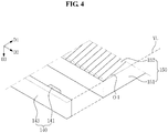
- FIG. 4 is an enlarged perspective view illustrating a modified exemplary embodiment of a light guide plate 150 relative to a light source unit 140 according to the invention.
- FIG. 4 is a perspective view illustrating an upper surface 150a and a light incident surface 150c of the light guide plate 150 according to an alternative exemplary embodiment.
- repeated description of the light guide plate 150 described above will be omitted from the description related to the light guide plate 150 of FIG. 4 .
- the light guide plate 150 may include a lens pattern 152 including a plurality of lenses disposed or formed on the body portion 151 so as to define the upper surface 150a of the light guide plate 150.
- the lenses of the lens pattern 152 may each extend with a tilting angle ⁇ 1 ranging from about 0.5 degrees to about 10 degrees with respect to a virtual line VL parallel to a first direction D 1.
- the light guide plate 150 is configured such that the plurality of lenses forming the collective lens pattern 152 as the upper surface 150a of the light guide plate 150 are inclined at a predetermined tilting angle ⁇ 1 with respect to the virtual line VL parallel to the first direction D1, and accordingly, a moire stain may be substantially prevented from appearing.
- FIG. 5 is a perspective view illustrating another exemplary embodiment of a light guide plate and a light source unit according to the invention
- FIG. 6 is an enlarged perspective view illustrating area "B" of FIG. 5
- FIG. 7 is an enlarged perspective view illustrating area "C” of FIG. 6
- FIG. 8 is a cross-sectional view taken along line I-I' of FIG. 7
- FIGS. 5 and 6 are perspective views illustrating the lower surface 150b and the light incident surface 150c of the light guide plate 150 according to an exemplary embodiment.
- the light guide plate 150 may include a prism pattern 153 disposed or formed at the lower surface 150b of the light guide plate 150.
- the prism pattern 153 may include a plurality of prisms as a material or layer separate from that of the body portion 151, but the invention is not limited to.
- the prisms of the prism pattern 153 may be defined by portions of the body portion 151.
- the prism pattern 153 may include a plurality of prisms, including prism 153a, prism 153b and prisms therebetween, arranged one behind another along the first direction D1 perpendicular to the light incident surface 150c.
- a number of single or separated prisms may be arranged along the first direction D1.
- the prisms arranged one behind another along the first direction D1 may form a single group of prisms.
- a single prism 153a, 153b respectively may be arranged along the second direction D2.
- Each prism among the prism 153a, the prism 153b and prisms therebetween may have a length which extends in the second direction D2 parallel to the light incident surface 150c.
- the prisms are discrete shapes disposed spaced apart from each other.
- the lengths of the plurality of prisms arranged along the first direction D1 may increase gradually as a distance from the light incident surface 150c increases. That is, a length 11 of a (first) prism 153a adjacent to (e.g., closest to) the light incident surface 150c is the smallest and a length 12 of a (last) prism 153b disposed adjacent to (e.g., closest to) the light opposing surface 150d is the largest.
- Each of the prisms of the prism pattern 153 may have a length ranging from about 3 ⁇ m to about 300 ⁇ m. Lengths of the prisms within a prism pattern 153 increase as a distance of the prisms from the light incident surface 150c increases.
- the prisms of the prism pattern 153 may be formed in at least one of an engraved (e.g., recessed) form and an embossed (e.g., protruded) form, relative to a common surface of the body portion 151 of the light guide plate 150.
- the prisms of the prism pattern 153 according to an exemplary embodiment are assumed to be engraved (e.g., recessed) patterns, extended into the body portion 151 of the light guide plate 150 from a lowermost surface 150b of the overall light guide plate 150. That is, it is considered that the body portion 151 extends to include a portion (or layer) of the light guide plate 150 in which the prisms are recessed. Inclined surfaces of the prisms and the lower surface of the body portion 151 may together form the lower surface 150b of the overall light guide plate 150. Portions of the lower surface 150b which are between the prisms are coplanar with each other.
- the prism pattern 153 as a group of prisms arranged in the first direction D1, may be provided in plurality along a second direction D2 parallel to the light incident surface 150c.
- a pitch P1 between the plurality of prism patterns 153 disposed adjacently along the second direction D2 may be in a range of about 50 ⁇ m to about 300 ⁇ m.
- the pitch P1 is taken between same positions among the prisms within a group of prisms arranged in the first direction D1 defining the prism pattern 153, such as being between virtual lines taken commonly at the center of each prism, but not being limited thereto.
- prisms 153c and 153d are disposed between the first and last prisms 153a and 153b.
- Each of the prisms 153a through 153b within a prism pattern 153 have a width W2 in a range from about 3 ⁇ m to about 30 ⁇ m in the first direction D1.
- the each of the prisms 153a through 153b may be spaced apart from each other by a predetermined pitch P2 in the first direction D1.
- the pitch P2 is taken between same positions among the prisms within a group of prisms arranged in the first direction D1 defining the prism pattern 153, such as being between edges of the prisms closest to the light incident surface 150c.
- FIGS. 7 and 8 illustrate that the pitch P2 between the prisms 153c and 153d disposed adjacent to each other in the first direction D1 is substantially the same, but exemplary embodiments are not limited thereto.
- the pitch P2 between the prisms 153c and 153d disposed adjacent to each other in the first direction D1 may decrease from the light incident surface 150c toward the light opposing surface 150d, as a distance from the light incident surface 150c increases.
- Each of the prisms within a group of prisms arranged in the first direction D1 defining the prism pattern 153 includes inclined surfaces extending from the lower surface 150b of the light guide plate 150.
- an angle ⁇ 2 between inclined surfaces 153c' and 153d' of the prisms 153c and 153d, and the lower surface 150b of the light guide plate 150, respectively may be in a range from about 127 degrees to about 134 degrees.
- the inclined surfaces 153c' and 153d' of the prisms such as 153c and 153d may be parallel to each other along an entirety of the length of such prisms, but are not limited thereto.
- the light guide plate 150 includes, at the lower surface 150b thereof, the plurality of prisms within a single prism pattern 153 that increase gradually in length as prisms are position along the first direction from the light incident surface 150c toward the light opposing surface 150d, so that light emitted through the light guide plate 150 may be uniformly provided to the display panel.
- the light provided from the light source unit 140 becomes weaker from the light incident surface 150c toward the light opposing surface 150d, such that lengths of the plurality of prisms within a single prism pattern 153 increase gradually from the light incident surface 150c toward the light opposing surface 150d.
- an amount of light reflected at the prism closer to the light incident surface 150c is reduced and an amount of light reflected at the prism closer to the light opposing surface 150d is increased.
- the length of the prism 153a disposed closest to the light incident surface 150c is substantially minimized and the lengths of remaining prisms within the single prism pattern 153 gradually increase to the prism 153b, so that uniform light may be provided to the display panel 120.
- FIG. 9 is an enlarged perspective view illustrating a modified exemplary embodiment of a light guide plate 150 according to the invention
- FIG. 10 is a cross-sectional view taken along line II-II' of FIG. 9.
- FIGS. 9 and 10 are perspective views illustrating a portion of a lower surface 150b of the light guide plate 150 according to an alternative exemplary embodiment. For convenience of explanation, repeated description of the light guide plate 150 in FIGS. 5 through 8 will be omitted from the description related to the light guide plate 150 of FIGS. 9 and 10 .
- the light guide plate 150 may include a prism pattern 153 disposed or formed at the lower surface 150b.
- the prism pattern 153 may be disposed or formed in at least one of an engraved (e.g., recessed) form and an embossed (e.g., protruded) form.
- the prisms of the prism pattern 153 according to an alternative exemplary embodiment is assumed to be a protruded pattern extended away from a main portion of the body portion 151 of the light guide plate 150 from a lower surface of the body portion 151 which is common to each prism.
- a portion of the body portion 151 extends to define the protruded prisms of the prism pattern 153. Inclined surfaces of the prisms and the portions of the body portion 151 therebeteween may together form the lower surface 150b of the overall light guide plate 150. Portions of the lower surface of the body portion 151 which are between the prisms are coplanar with each other.
- prisms 153e and 153f are arranged one behind another along a first direction D1 perpendicular to a light incident surface (not illustrated).
- the prisms 153e and 153f may have lengths 13 and 14 which extend in a second direction D2 parallel to the light incident surface 150c.
- the prisms 153e and 153f may represent a pair of prisms within a single prism pattern 153, such as being between a first prism closest to the light incident surface 150c and a second prism closest to the light opposing surface 150c.
- the lengths of the plurality of prisms arranged along the first direction D1 may increase gradually from the light incident surface 150c toward the light opposing surface 150d.
- the lengths 13 and 14 of the plurality of prisms 153e and 153f arranged along the first direction D1 may increase gradually toward the first direction D1. That is, lengths of the prisms represented by prisms 153e and 153f within a prism pattern 153 increase as a distance of the prisms from the light incident surface 150c increases.
- Each of the prisms within a prism pattern 153 such as represented by prisms 153e and 153f, may have a length in a range from about 3 ⁇ m to about 300 ⁇ m.
- each of the prisms 153e and 153f may have a width W2 in a range from about 3 ⁇ m to about 30 ⁇ m in the first direction D1.
- the prisms 153e and 153f may be spaced apart from each other by a predetermined pitch P2 in the first direction D 1.
- Each of the prisms within a group of prisms arranged in the first direction D1 defining the prism pattern 153 includes inclined surfaces extending from the lower surface 150b of the body portion 151 of the light guide plate 150.
- an angle ⁇ 2 between inclined surfaces 153e' and 153f of the prisms 153e and 153f and the lower surface 150b of the body portion 151 of the light guide plate 150 may be in a range from about 127 degrees to about 134 degrees.
- the inclined surfaces 153e' and 153f of the prisms such as 153e and 153f may be parallel to each other along an entirety of the length of such prisms, but are not limited thereto.
- the light guide plate 150 includes, as the lower surface 150b of the light guide plate 150, the plurality of prisms 153e and 153f extended from a lower surface of the body portion 151, that increase gradually in length from the light incident surface 150c toward the light opposing surface 150d so that light emitted through the light guide plate 150 may be uniformly provided to the display panel 120.
- FIG. 11 is an enlarged perspective view illustrating a modified exemplary embodiment of a portion of a light guide plate according to the invention.
- FIG. 11 is a perspective view illustrating a lower surface 150b and a light incident surface 150c of the light guide plate 150 according to an alternative exemplary embodiment.
- repeated description of the light guide plate 150 according to previous exemplary embodiments will be omitted from the description related to the light guide plate 150 of FIG. 11 .
- the light guide plate 150 may include a prism pattern 153 disposed or formed at the lower surface 150b.
- the prism pattern 153 may include a plurality of prisms arranged one behind another along a common center line CL tilted by an angle ⁇ 3 ranging from about 0.5 degrees to about 10 degrees with respect to a virtual line VL parallel to a first direction D1.
- the prisms of a prism pattern 153 may be aligned along the center line CL.
- Each prism within a single prism pattern 153 may by symmetrical with respect to the center line CL.
- Each prism within a prism pattern 153 may have a center thereof defined along the second direction, and the center line CL extends through the center of each prism.
- lengths of the prisms may increase gradually as a distance from the light incident surface 150c increases toward the first direction D1.
- the prism pattern 153 may be provided in plurality along a second direction D2.
- the light guide plate 150 is configured such that an arrangement line of the prisms within the prism pattern 153 disposed or formed at the lower surface 150b has a predetermined tilting angle ⁇ 3 with respect to the virtual line VL parallel to the first direction D1, and accordingly, moire stains may be substantially prevented from appearing.
- FIG. 12 is an enlarged perspective view illustrating another modified exemplary embodiment of a portion of a light guide plate 150 according to the invention
- FIG. 13 is an enlarged perspective view illustrating still another modified exemplary embodiment of a light guide plate 150 according to the invention.
- FIGS. 12 and 13 are perspective views illustrating a lower surface 150b and a light incident surface 150c of the light guide plate 150 according to an alternative exemplary embodiment. For convenience of explanation, repeated description of the light guide plate 150 according to previous exemplary embodiments will be omitted from the description related to the light guide plate 150 in FIGS. 12 and 13 .
- the light guide plate 150 may include a prism pattern 153 disposed or formed at the lower surface 150b.
- the prism pattern 153 may include a plurality of prisms arranged one behind another along a first direction D1, and lengths of the prisms may increase gradually as a distance from the light incident surface 150c increase one behind another toward the first direction D1.
- the prism pattern 153 may be provided in plurality along a second direction D2.
- the light guide plate 150 may further include a light scattering pattern 154 between the prism patterns 153.
- the light scattering pattern 154 may be disposed between the prisms within a prism pattern 153.
- the light scattering pattern 154 may be provided in plural to have a discrete shape such as a hairline (e.g., non-linear line) shape (see FIG. 12 ) or a dot shape (see FIG. 13 ).
- the light scattering patterns 154 are discrete shapes disposed spaced apart from each other. The light scattering patterns 154 scatter light passing through the inside of the light guide plate 150 to allow the light to be emitted through an upper surface 150a of the light guide plate 150.
- the light scattering patterns 154 are disposed or formed at the lower surface 150b of the light guide plate 150 so that a certain portion of the light guide plate 150 does not appears as a bright portion or a dark portion because at the light scattering patterns 154, light may be condensed at or may not reach the certain portion may be canceled out. That is, the light scattering patterns 154 may control the occurrence of the light or dark portion generated because of the interference of light due to a light path difference.
- a quantity of the light scattering pattern 154 in a unit area may be gradually reduced as a distance from the light incident surface 150c toward the light opposing surface 150d increases.
- the light guide plate 150 includes the prism pattern 153 at the lower surface 150b, where lengths of the prisms of the prism pattern 153 increase from the light incident surface 150c toward the light opposing surface 150d, an area of the light guide plate 150 adjacent to the light incident surface 150c may appear as a relatively dark portion. Accordingly, the light scattering pattern 154 is formed at a region adjacent to the light incident surface 150c, to have a greater density, so that light may be uniformly emitted from an entire surface of the light guide plate 150.
- such a light scattering pattern 154 may be formed by processing a surface using a sand blaster or by applying a paint that scatters light. That is, the light scattering pattern 154 may be recessed from the lower surface 150b of the light guide plate 150 or may be protruded from the lower surface of the body portion 151.
- FIG. 14 is an enlarged perspective view illustrating yet another modified embodiment of a portion of a light guide plate 150 according to the invention.
- FIG. 14 is a perspective view illustrating a lower surface 150b of the light guide plate 150 according to an alternative exemplary embodiment.
- repeated description of the light guide plate 150 according to previous exemplary embodiments will be omitted from the description related to the light guide plate 150 in FIG. 14 .
- the light guide plate 150 may include a prism pattern 153 disposed or formed at the lower surface 150b.
- the prism pattern 153 may include a plurality of prisms, such as 153g and 153h, arranged one behind another along a first direction D1.
- lengths of the prisms in a second direction D2 may increase gradually as a distance of the prisms from the light incident surface 150c increases in the first direction D1.
- the invention is not restricted to a single pair of prisms but there may be a plurality of prisms respectively there might be a plurality of pairs of prisms.
- Inclined surfaces 153g' and 153h' of the prisms 153g and 153h disposed adjacent to each other in the first direction D1 may be formed to be not parallel to each other or to the second direction D2. That is, each of the prisms 153g and 153h may have irregularly shaped inclined surfaces 153g' and 153h'. That is, the inclined surfaces 153g' and 153h' of the prisms such as 153g and 153h may not be parallel to each other along an entirety of the length of such prisms, but are not limited thereto.
- the light guide plate 150 includes the plurality of prisms such as 153g and 153h including the irregularly shaped inclined surfaces 153g' and 153h', and accordingly, moire stains may be substantially prevented from appearing.
- an overall thickness of a display device may be reduced by omitting the optical sheet of a conventional display device, and the manufacturing costs may be reduced.
- the display device may collimate the light emitted from the light source and substantially prevent the light guide plate from being visible, by the light guide plate including the lens pattern on the upper (light emission) surface of the light guide plate.
- the light guide plate of the display device includes the prism pattern on the lower surface of the light guide plate so that light emitted from the light guide plate may be uniformly provided to the display panel.
- the display device may substantially prevent moire stains from appearing by the light guide plate including discrete patterns disposed or formed at the upper and lower surfaces of the light guide plate tilted or having no regularity.
Landscapes
- Physics & Mathematics (AREA)
- General Physics & Mathematics (AREA)
- Optics & Photonics (AREA)
- Nonlinear Science (AREA)
- Mathematical Physics (AREA)
- Chemical & Material Sciences (AREA)
- Crystallography & Structural Chemistry (AREA)
- Engineering & Computer Science (AREA)
- Microelectronics & Electronic Packaging (AREA)
- Planar Illumination Modules (AREA)
Abstract
Description
- Exemplary embodiments of the invention relate to a display device having relative lightweight, thinness and high luminance.
- Liquid crystal display ("LCD") devices are one of most widely used types of flat panel display ("FPD") devices. An LCD device includes two substrates including electrodes therein and a liquid crystal layer interposed therebetween. Upon applying voltage to the two electrodes, liquid crystal molecules of the liquid crystal layer are rearranged such that an amount of transmitted light is controlled in the LCD device.
- An LCD device, which is a passive light emitting device, includes a display panel which displays an image and a backlight unit for providing light to the display panel. The backlight unit is classified into a direct type backlight unit, an edge type backlight unit and a corner type backlight unit according to the position of the light source within the LCD device.
- The edge type backlight unit is widely used because it is relatively easy to manufacture, light in weight and low in power consumption as compared to the direct type backlight unit. In the edge type backlight unit, a plurality of optical sheets for diffusing and collimating light provided from the light source may be disposed as a separate element between a light guide plate and the display panel.
- Exemplary embodiments of the invention are directed to a display device which has a reduced overall thickness by omitting an optical sheet separate from a light guide plate and substantially prevents degradation in image quality.
- According to an exemplary embodiment, a display device includes: a display panel which displays an image with light; a light source which generates the light; and a light guide plate which receives the light from the light source and provides the light to the display panel. The light guide plate includes: an upper surface facing the display panel, the upper surface including a lens pattern, a lower surface opposing the upper surface, the lower surface including a prism pattern, a light incident surface facing the light source, and a light opposing surface opposing the light incident surface. The prism pattern includes a plurailty of prisms arranged one behind another along a line extended in a first direction from the light incident surface to the light opposing surface, each of the prisms has a length extending in a second direction along a length of the light incident surface, and among the prisms arranged along the line extended in the first direction within the prism pattern, the lengths of the prisms increase as a distance from the light incident surface increases. This means, that the line along which the prisms of a prism pattern are arranged may be parallel to a first direction perpendicular to the second direction and perpendicular to the length of the light incident surface. However, according to another embodiment, the line may extend partially in the first direction and partially in the second direction which means may be tilted with respect to a virtual line extended in the first direction perpendicular to a length of the light incident surface. The line may be a center line which means that the line extends through a center of the prisms with regards to a length direction of the prisms. The prisms may be arranged parallel to each other and with their length direction inclined to the first and the second directions or with their length direction parallel to the second direction, especially parallel to the length direction of the light incident surface.
- The prism may be a recessed portion of the light guide plate or a protruded portion of the light guide plate.
- The length of the prism may be in a range from about 3 µm (micrometers) to about 300 µm.
- The prism may include an inclined surface extended from the lower surface of the light guide plate. The inclined surface of the prism may form an angle ranging from about 127 degrees to about 134 degrees with respect to the lower surface.
- For prisms arranged adjacent to each other along the line extended in the first direction, the inclined surfaces thereof may be not plane to each other or not parallel to the second direction. In other words, the inclined surfaces may be uneven. The length extension of the inclined surfaces may be not parallel to each other or not parallel to the second direction.
- Each of the prisms may have a width extending in the first direction, and the width may range from about 3 µm to about 30 µm.
- A pitch may be defined in the first direction or in the direction of the line along which the prisms are arranged between prisms arranged adjacent to each other along the first direction respectively along the line.
- The prism pattern may be provided in plurality arranged along the second direction. This means a plurality of prism patterns may be arranged along the second direction.
- A pitch may be defined in the second direction between a first prism of a first prism pattern and a second prism of a second prism pattern arranged adjacent to each other along the second direction, and the pitch may be in a range from about 50 µm to about 300 µm.
- The lens pattern may include a lens provided in plurality arranged along the second direction, each of the lenses having a semicircular or semi-elliptical cross-section and a length extending in the first direction. This means the lens pattern may comprise a plurality of lenses arranged along the second direction.
- The lens may have a width extending in the second direction, the width ranging from about 3 µm to about 30 µm.
- The lens may have a height extending from the upper surface of the light guide plate, the height ranging from about 3 µm to about 15 µm.
- The prism pattern may be provided in plurality along the second direction, and a light scattering pattern or a plurality of light scattering patterns may be provided between the prism patterns.
- The light scatterning pattern may be disposed along the first direction and a density of the light scattering pattern may be reduced as the distance from the light incident surface increases. If the light scattering pattern disposed along the first direction is defined as a plurality of (differrent) light scattering patterns arranged along the first direction, then among the light scattering patterns arranged along the first direction, a density of the light scattering patterns may be reduced as the distance from the light incident surface increases.
- The light scattering pattern may have a discrete non-linear shape. This means, the light scattering pattern comprises elements defining the pattern and the elements have a non-linear form.
- The light scattering pattern may have a discrete dot shape. This means that elements forming the light scattering pattern have a dot shape.
- According to another exemplary embodiment, a display device includes: a display panel which displays an image with light; a light source which generates the light; and a light guide plate which receives the light from the light source and provides the light to the display panel. The light guide plate includes: an upper surface facing the display panel, the upper surface including a lens pattern, a lower surface opposing the upper surface, the lower surface including a prism pattern, a light incident surface facing the light source, and a light opposing surface opposing the light incident surface. A virtual line is defined extended in a first direction from the light incident surface to the light opposing surface, the virtual line perpendicular to a length of the light incident surface, the prism pattern includes a prism provided in plurality arranged along a center line extended in the first direction, the center line tilted by an angle ranging from about 0.5 degrees to about 10 degrees with respect to the virtual line, each of the prisms has a length extending in a second direction along the length of the light incident surface, and among the prisms arranged along the center line tilted with respect to the virtual line, the lengths of the prisms increase as a distance from the light incident surface increases.
- According to another exemplary embodiment, a display device includes: a display panel which displays an image with light; a light source which generates the light; and a light guide plate which receives the light from the light source and provides the light to the display panel. The light guide plate includes: an upper surface facing the display panel, the upper surface comprsing a lens pattern, a lower surface opposing the upper surface, the lower surface incluidng a prism pattern, a light incident surface facing the light source, and a light opposing surface opposing the light incident surface. The prism pattern of the lower surface of the light guide plate includes a plurality of prisms arranged along a first direction from the light incident surface to the light opposing surface, each of the prisms has a length extending in a second direction along a length of the light incident surface, among the prisms arranged along the first direction within the prism pattern, the lengths of the prisms increase as a distance from the light incident surface increases, and with respect to a virtual line extended in the first direction to be perpendicular to the length of the light incident surface, the lens pattern of the upper surface of the light guide plate has a length forming a tilting angle ranging from about 0.5 degrees to about 10 degrees with respect to the virtual line.
- The foregoing is illustrative only and is not intended to be in any way limiting. In addition to the illustrative features, exemplary embodiments and features described above, further features, exemplary embodiments and features will become apparent by reference to the drawings and the following detailed description.
- A more complete appreciation of the invention will become more apparent by describing in detail exemplary embodiments thereof with reference to the accompanying drawings, where:
-
FIG. 1 is an exploded perspective view illustrating an exemplary embodiment of a display device according to the invention; -
FIG. 2 is a perspective view illustrating an exemplary embodiment of a light guide plate and a light source unit according to the invention; -
FIG. 3 is an enlarged perspective view illustrating area "A" ofFIG. 2 ; -
FIG. 4 is an enlarged perspective view illustrating a modified exemplary embodiment of a light guide plate and a light source unit according to the invention; -
FIG. 5 is a perspective view illustrating another exemplary embodiment of a light guide plate and a light source unit according to the invention; -
FIG. 6 is an enlarged perspective view illustrating area "B" ofFIG. 5 ; -
FIG. 7 is an enlarged perspective view illustrating area "C" ofFIG. 6 ; -
FIG. 8 is an enlarged cross-sectional view taken along line I-I' ofFIG. 7 ; -
FIG. 9 is an enlarged perspective view illustrating a modified exemplary embodiment of a light guide plate according to the invention; -
FIG. 10 is an enlarged cross-sectional view taken along line II-II' ofFIG. 9 ; and -
FIGS. 11 ,12 ,13 and14 are enlarged perspective views illustrating modified exemplary embodiments of a light guide plate relative to a light source unit according to the invention. - Exemplary embodiments will now be described more fully hereinafter with reference to the accompanying drawings. Although the invention may be modified in various manners and have several exemplary embodiments, exemplary embodiments are illustrated in the accompanying drawings and will be mainly described in the specification. However, the scope of the invention is not limited to the exemplary embodiments and should be construed as including all the changes, equivalents and substitutions included in the scope of the invention.
- In the drawings, thicknesses of a plurality of layers and areas are illustrated in an enlarged manner for clarity and ease of description thereof. When a layer, area, or plate is referred to as being related to another elements such as being "on" another layer, area, or plate, it may be directly on the other layer, area, or plate, or intervening layers, areas, or plates may be present therebetween. Conversely, when a layer, area, or plate is referred to as being related to another element such as being "directly on" another layer, area, or plate, intervening layers, areas, or plates are absent therebetween. Further when a layer, area, or plate is referred to as being related to another element such as being "below" another layer, area, or plate, it may be directly below the other layer, area, or plate, or intervening layers, areas, or plates may be present therebetween. Conversely, when a layer, area, or plate is referred to as being related to another elements such as being "directly below" another layer, area, or plate, intervening layers, areas, or plates are absent therebetween.
- The spatially relative terms "below," "beneath," "less," "above," "upper" and the like, may be used herein for ease of description to describe the relations between one element or component and another element or component as illustrated in the drawings. It will be understood that the spatially relative terms are intended to encompass different orientations of the device in use or operation, in addition to the orientation depicted in the drawings. For example, in the case where a device illustrated in the drawing is turned over, the device positioned "below" or "beneath" another device may be placed "above" another device. Accordingly, the illustrative term "below" may include both the lower and upper positions. The device may also be oriented in the other direction and thus the spatially relative terms may be interpreted differently depending on the orientations.
- Throughout the specification, when an element is referred to as being "connected" to another element, the element is "mechanically or physically" to the other element, or "electrically connected" to the other element with one or more intervening elements interposed therebetween.
- The terminology used herein is for the purpose of describing particular embodiments only and is not intended to be limiting. As used herein, the singular forms "a," "an," and "the" are intended to include the plural forms, including "at least one," unless the content clearly indicates otherwise. "At least one" is not to be construed as limiting "a" or "an." "Or" means "and/or." As used herein, the term "and/or" includes any and all combinations of one or more of the associated listed items. It will be further understood that the terms "comprises," "comprising," "includes" and/or "including," when used in this specification, specify the presence of stated features, integers, steps, operations, elements and/or components, but do not preclude the presence or addition of one or more other features, integers, steps, operations, elements, components and/or groups thereof.
- It will be understood that, although the terms "first," "second," "third," and the like may be used herein to describe various elements, these elements should not be limited by these terms. These terms are only used to distinguish one element from another element. Thus, "a first element" discussed below could be termed "a second element" or "a third element," and "a second element" and "a third element" may be termed likewise without departing from the teachings herein.
- "About" or "approximately" as used herein is inclusive of the stated value and means within an acceptable range of deviation for the particular value as determined by one of ordinary skill in the art, considering the measurement in question and the error associated with measurement of the particular quantity (i.e., the limitations of the measurement system). For example, "about" may mean within one or more standard deviations, or within ± 30%, 20%, 10% or 5% of the stated value.
- Unless otherwise defined, all terms used herein (including technical and scientific terms) have the same meaning as commonly understood by those skilled in the art to which this invention pertains. It will be further understood that terms, such as those defined in commonly used dictionaries, should be interpreted as having a meaning that is consistent with their meaning in the context of the relevant art and will not be interpreted in an ideal or excessively formal sense unless clearly defined in the present specification.
- Some of the parts which are not associated with the description may not be provided in order to specifically describe exemplary embodiments of the invention and like reference numerals refer to like elements throughout the specification.
- A conventional display device including a plurality of optical sheets between a light guide plate and a display panel to control a direction of light provided to the display panel, has an increased overall thickness owing to the plurality of optical sheets disposed as separate elements from the light guide plate and the display panel. Therefore, there exists an increasing tendency to omit the plurality of optical sheets between the light guide plate and the display panel, thereby forming a slimmer display device.
- Although a display device is described as being an LCD device in exemplary embodiments, exemplary embodiments are not limited thereto, and a display device in which a display panel that receives light from a backlight unit to display an image may be included in the scope of the invention.
-
FIG. 1 is an exploded perspective view illustrating an exemplary embodiment of a display device according to the invention. - Referring to
FIG. 1 , the display device according to an exemplary embodiment includes anupper frame 110, adisplay panel 120, anintermediate frame 130, alight source unit 140, alight guide plate 150, areflection sheet 160 and alower frame 170. - Hereinafter, the
intermediate frame 130, thelight source unit 140, thelight guide plate 150, thereflection sheet 160 and thelower frame 170 are collectively referred to as a backlight unit. - The
upper frame 110 has an opening window defined therein for exposing an active area of thedisplay panel 120 to outside the display device and is disposed so as to cover a front edge and a side surface of thedisplay panel 120. Theupper frame 110 may include a relatively rigid metal material such as stainless steel or a material having relatively good heat dissipation properties such as aluminum or an aluminum alloy. - The
display panel 120 may be provided in a quadrangular plate shape and receive an electric signal from outside thereof to display an image. Thedisplay panel 120 may include a first (display)substrate 121, a second (display)substrate 123 opposing thefirst substrate 121, an optical control layer such as a liquid crystal layer (not illustrated) between thefirst substrate 121 and thesecond substrate 123, or the like. - The
first substrate 121 includes a plurality of pixel electrodes arranged in a matrix, a switching element such as a thin film transistor applying a driving voltage to each of the pixel electrodes, and various signal lines for driving the pixel electrodes and the thin film transistor. - The
second substrate 123 is disposed to oppose thefirst substrate 121. Thesecond substrate 123 includes a common electrode including a transparent conductive material and a color filter. The color filter may include red, green and blue color filters. - The liquid crystal layer (not illustrated) is interposed between the
first substrate 121 and thesecond substrate 123. An orientation of molecules of the liquid crystal layer is rearranged by an electric field formed between the pixel electrode and the common electrode. As such, the rearranged liquid crystal layer adjusts or controls the transmittance of light emitted from the backlight unit, and the adjusted light passes through the color filter to display an image to outside thedisplay panel 120. - In addition, a lower polarizer (not illustrated) may be disposed on a rear surface of the
first substrate 121 and an upper polarizer (not illustrated) may be disposed on an upper surface of thesecond substrate 123. The upper polarizer and the lower polarizer may have a total planar area corresponding to that of thedisplay panel 120. - The upper polarizer may transmit only a specific polarized light among light arriving from the outside the display panel and absorb or block the remaining light. The lower polarizer plate may transmit only a specific polarized light among the light output from the backlight unit, and absorb or block the remaining light.
- A driving
circuit board 125 may be disposed on at least one side of thedisplay panel 120. The drivingcircuit board 125 may generate and/or apply various control signals or a power signal for driving thedisplay panel 120. - The
display panel 120 and the drivingcircuit board 125 may be electrically connected to each other by at least one flexible printed circuit board ("FPCB") 127. TheFPCB 127 may be a chip on film ("COF") or a tape carrier package ("TCP"). The number of theFPCBs 127 may have various values depending on the size and driving scheme of thedisplay panel 120. - A
driving chip 129 may be mounted on theFPCB 127. Thedriving chip 129 may generate various driving signals for driving thedisplay panel 120. Thedriving chip 129 may be represented by a driver integrated circuit ("IC") or a source IC in which a timing controller and/or a data driving circuit are integrated into one chip. - The
intermediate frame 130 may support a rear edge of thedisplay panel 120 and may accommodate thelight source unit 140, thelight guide plate 150, thereflection sheet 160, or the like. - The
intermediate frame 130 may have a polygonal frame shape in which a hollow space is defined. In an exemplary embodiment, for example, theintermediate frame 130 may have a quadrangular frame shape in which an empty space is defined. Theintermediate frame 130 may be formed as a single, unitary member or may be formed from a plurality of separately provided pieces as required and then assembled. Theintermediate frame 130 may include a flexible material such as plastic, or may be formed as an injection molded member such as through an injection molding process or the like. - The
light source unit 140 includes alight source 141 and alight source substrate 143 on which thelight source 141 is disposed. - The
light source 141 may be disposed at an edge or one side surface of thelight guide plate 150. That is, thelight source 141 may generate and emit light to the edge or one side surface of thelight guide plate 150. Thelight source 141 may include at least one light emitting diode ("LED") chip (not illustrated) and a package (not illustrated) for accommodating the LED chip. In an exemplary embodiment, for example, the LED chip (not illustrated) may be a gallium nitride (GaN)-based LED chip emitting a blue light. - The number of the
light sources 141 may have various values in consideration of the size of thedisplay panel 120, luminance uniformity, or the like. Thelight source substrate 143 may be a printed circuit board ("PCB") or a metal printed circuit board ("metal PCB"). - The
light source unit 140 may be disposed or formed on one side surface, opposite side surfaces or all four side surfaces of thelight guide plate 150 in consideration of the size and luminance uniformity of thedisplay panel 120. That is, thelight source unit 140 may be disposed or formed on at least one of edge portions of thelight guide plate 150. Herein, thelight source unit 140 is assumed to be disposed on one side surface of thelight guide plate 150. - Although not illustrated in
FIG. 1 , a wavelength conversion unit (not illustrated) may be disposed between thelight source unit 140 and the light incident surface of thelight guide plate 150. The wavelength conversion unit (not illustrated) may include a material for converting the wavelength of light emitted from thelight source unit 140. In an exemplary embodiment, for example, the wavelength conversion unit may convert the wavelength of a blue light emitted from a blue LED light source into a white light. - Although described as a plate, such as having a relatively large cross-sectional thickness for ease of description, for convenience of explanation, the
light guide plate 150 may be formed in the form of a sheet or a film for slimming down the display device. Thelight guide plate 150 may be provided in a sheet or film shape for which the cross-sectional thickness is smaller than that of the plate and is relatively small as compared to the planar size thereof, That is, thelight guide plate 150 may include both a plate and a film for guiding light. - Hereinafter, one surface of the
light guide plate 150 facing thedisplay panel 120 is referred to as anupper surface 150a, another surface of thelight guide plate 150 opposing theupper surface 150a is referred to as alower surface 150b, another surface of thelight guide plate 150 facing thelight source unit 140 is referred to as alight incident surface 150c, and another surface of thelight guide plate 150 opposing thelight incident surface 150c is referred to as alight opposing surface 150d. Side surfaces of thelight guide plate 150 connecting theupper surface 150a and thelower surface 150b to each other, and thelight incident surface 150c may respectively be one of the side surfaces. Light is emitted from thelight guide plate 150 through theupper surface 150a and light is incident into thelight guide plate 150 through thelight incident surface 150c. - For convenience of explanation, a direction perpendicular to the
light incident surface 150c is referred to as a first direction D1, a direction along which a length of thelight incident surface 150c extends is referred to as a second direction D2, and a thickness direction of thelight guide plate 150 is referred to as a third direction D3. The display device and components thereof are disposed in a plane defined by the first and second directions D1 and D2, while a thickness of the display device and components thereof are taken in the third direction D3. - The
light guide plate 150 according to an exemplary embodiment may include abody portion 151 and alens pattern 152 disposed or formed on thebody portion 151. - The
body portion 151 may include a material having a light transmitting property, such as an acrylic resin, e.g., polymethylmethacrylate ("PMMA"), polycarbonate, and a tempered glass, so as to efficiently guide the light. Thebody portion 151 may define portions of side surfaces and/or thelower surface 150b of thelight guide plate 150. - The
lens pattern 152 disposed or formed on thebody portion 151 may include a hard coating exclusive resin, and the resin may be ultraviolet ("UV")-cured to have properties similar to polycarbonate. The resin may include an oligomer, a monomer, a photoinitiator, silicone, or the like, and may be classified into a soft resin and a hard resin depending on the content of the silicone and monomer. - The details of the shape of the plurality of lenses within the
lens pattern 152 disposed or formed on thebody portion 151 will be described below. - The
reflection sheet 160 may include, for example, polyethylene terephthalate ("PET") and be reflective, and one surface of thereflection sheet 160 may be coated with a diffusion layer including, for example, titanium dioxide. In addition, thereflection sheet 160 may include a material including a metal such as silver (Ag). - The
lower frame 170 may include a metal material having relatively good rigidity and heat dissipation characteristics. In an exemplary embodiment, for example, thelower frame 170 may include at least one selected from stainless steel, aluminum, an aluminum alloy, magnesium, a magnesium alloy, copper, a copper alloy and an electrogalvanized steel sheet. -
FIG. 2 is a perspective view illustrating the light guide plate and the light source unit according to an exemplary embodiment, andFIG. 3 is an enlarged perspective view illustrating area "A" ofFIG. 2. FIGS. 2 and3 are perspective views illustrating theupper surface 150a of thelight guide plate 150 and thelight incident surface 150c of thelight guide plate 150 according to an exemplary embodiment. - Referring to
FIGS. 2 and3 , thelight guide plate 150 according to an exemplary embodiment may include thelens pattern 152 extended from an upper surface of thebody portion 151 such as to define theupper surface 150a of thelight guide plate 150. Each of the lenses of thelens pattern 152 may be lengthwise elongated in the first direction D1, and the lenses are arranged one behind another along the second direction D2. InFIG. 3 , numeral 152 is used to indicate a single lens for convenience of explanation, but numeral 152 may be considered as indicating the collection of lenses. Each lens may have a semicircular or semi-elliptical cross-section, but exemplary embodiments are not limited thereto. In an exemplary embodiment, for example, each lens may have a circular or triangular cross-section and the cross-sectional areas of the plurality of lenses may be different from each other. Alternatively, thelens pattern 152 may include a plurality of lenses elongated in the second direction D2 and arranged one behind another in the first direction D 1. The lenses of thelens pattern 152 extend from a common surface of thebody portion 151, such as from the upper surface thereof. Portions of the upper surface of thebody portion 151 which are between the lenses may be coplanar with each other. - A thickness t of the
body portion 151 according to an exemplary embodiment may be in a range from about 0.5 millimeter (mm) to about 3.5 millimeters (mm). As an example, when including PMMA or PC, thebody portion 151 may have a thickness t in a range from about 2.0 mm to about 3.5 mm. As another example, when including a tempered glass, thebody portion 151 may have a thickness t in a range from about 0.5 mm to about 1.5 mm. - The lens according to an exemplary embodiment may have a width W1 ranging from about 3 micrometers (µm) to about 30 µm in the second direction D2 and a height H1 ranging from about 3 µm to about 15 µm in the third direction D3.
FIG. 2 and3 illustrate that lenses disposed adjacent to each other in the second direction D2 are continuously formed, that is, having no space therebetween. However, exemplary embodiments are not limited thereto, and the plurality of lenses may be disposed or formed at a predetermined distance from each other in the second direction D2. - The
light guide plate 150 according to an exemplary embodiment includes thelens pattern 152 as theupper surface 150a of thelight guide plate 150 so that light emitted from thelight guide plate 150 may be collimated and thelight guide plate 150 may not be visible from the outside. -
FIG. 4 is an enlarged perspective view illustrating a modified exemplary embodiment of alight guide plate 150 relative to alight source unit 140 according to the invention. For example,FIG. 4 is a perspective view illustrating anupper surface 150a and alight incident surface 150c of thelight guide plate 150 according to an alternative exemplary embodiment. For convenience of explanation, repeated description of thelight guide plate 150 described above will be omitted from the description related to thelight guide plate 150 ofFIG. 4 . - Referring to
FIG. 4 , thelight guide plate 150 according to an alternative exemplary embodiment may include alens pattern 152 including a plurality of lenses disposed or formed on thebody portion 151 so as to define theupper surface 150a of thelight guide plate 150. In a top plan view of the plane defined by the first and second directions D1 and D2, the lenses of thelens pattern 152 may each extend with a tilting angle θ1 ranging from about 0.5 degrees to about 10 degrees with respect to a virtual line VL parallel to a first direction D 1. - As such, the
light guide plate 150 according to an alternative exemplary embodiment is configured such that the plurality of lenses forming thecollective lens pattern 152 as theupper surface 150a of thelight guide plate 150 are inclined at a predetermined tilting angle θ1 with respect to the virtual line VL parallel to the first direction D1, and accordingly, a moire stain may be substantially prevented from appearing. -
FIG. 5 is a perspective view illustrating another exemplary embodiment of a light guide plate and a light source unit according to the invention,FIG. 6 is an enlarged perspective view illustrating area "B" ofFIG. 5 ,FIG. 7 is an enlarged perspective view illustrating area "C" ofFIG. 6 , andFIG. 8 is a cross-sectional view taken along line I-I' ofFIG. 7 .FIGS. 5 and6 are perspective views illustrating thelower surface 150b and thelight incident surface 150c of thelight guide plate 150 according to an exemplary embodiment. - Referring to
FIGS. 5 and6 , thelight guide plate 150 according to an exemplary embodiment may include aprism pattern 153 disposed or formed at thelower surface 150b of thelight guide plate 150. Theprism pattern 153 may include a plurality of prisms as a material or layer separate from that of thebody portion 151, but the invention is not limited to. In an alternative embodiment, the prisms of theprism pattern 153 may be defined by portions of thebody portion 151. - The
prism pattern 153 may include a plurality of prisms, includingprism 153a,prism 153b and prisms therebetween, arranged one behind another along the first direction D1 perpendicular to thelight incident surface 150c. A number of single or separated prisms may be arranged along the first direction D1. The prisms arranged one behind another along the first direction D1 may form a single group of prisms. Asingle prism prism 153a, theprism 153b and prisms therebetween may have a length which extends in the second direction D2 parallel to thelight incident surface 150c. The prisms are discrete shapes disposed spaced apart from each other. - The lengths of the plurality of prisms arranged along the first direction D1 may increase gradually as a distance from the
light incident surface 150c increases. That is, a length 11 of a (first)prism 153a adjacent to (e.g., closest to) thelight incident surface 150c is the smallest and a length 12 of a (last)prism 153b disposed adjacent to (e.g., closest to) thelight opposing surface 150d is the largest. - Each of the prisms of the
prism pattern 153 may have a length ranging from about 3 µm to about 300 µm. Lengths of the prisms within aprism pattern 153 increase as a distance of the prisms from thelight incident surface 150c increases. - The prisms of the
prism pattern 153 according to an exemplary embodiment may be formed in at least one of an engraved (e.g., recessed) form and an embossed (e.g., protruded) form, relative to a common surface of thebody portion 151 of thelight guide plate 150. InFIGS. 5 through 8 , the prisms of theprism pattern 153 according to an exemplary embodiment are assumed to be engraved (e.g., recessed) patterns, extended into thebody portion 151 of thelight guide plate 150 from alowermost surface 150b of the overalllight guide plate 150. That is, it is considered that thebody portion 151 extends to include a portion (or layer) of thelight guide plate 150 in which the prisms are recessed. Inclined surfaces of the prisms and the lower surface of thebody portion 151 may together form thelower surface 150b of the overalllight guide plate 150. Portions of thelower surface 150b which are between the prisms are coplanar with each other. - The
prism pattern 153 as a group of prisms arranged in the first direction D1, may be provided in plurality along a second direction D2 parallel to thelight incident surface 150c. A pitch P1 between the plurality ofprism patterns 153 disposed adjacently along the second direction D2 may be in a range of about 50 µm to about 300 µm. The pitch P1 is taken between same positions among the prisms within a group of prisms arranged in the first direction D1 defining theprism pattern 153, such as being between virtual lines taken commonly at the center of each prism, but not being limited thereto. - Referring to
FIGS. 7 and 8 ,prisms last prisms prisms 153a through 153b within aprism pattern 153 have a width W2 in a range from about 3 µm to about 30 µm in the first direction D1. In addition, the each of theprisms 153a through 153b may be spaced apart from each other by a predetermined pitch P2 in the first direction D1. The pitch P2 is taken between same positions among the prisms within a group of prisms arranged in the first direction D1 defining theprism pattern 153, such as being between edges of the prisms closest to thelight incident surface 150c. -
FIGS. 7 and 8 illustrate that the pitch P2 between theprisms prisms light incident surface 150c toward thelight opposing surface 150d, as a distance from thelight incident surface 150c increases. - Each of the prisms within a group of prisms arranged in the first direction D1 defining the
prism pattern 153, includes inclined surfaces extending from thelower surface 150b of thelight guide plate 150. InFigure 8 , for example, an angle θ2 betweeninclined surfaces 153c' and 153d' of theprisms lower surface 150b of thelight guide plate 150, respectively, may be in a range from about 127 degrees to about 134 degrees. The inclined surfaces 153c' and 153d' of the prisms such as 153c and 153d may be parallel to each other along an entirety of the length of such prisms, but are not limited thereto. - As such, referring to
FIGS. 5 and6 once again, thelight guide plate 150 according to an exemplary embodiment includes, at thelower surface 150b thereof, the plurality of prisms within asingle prism pattern 153 that increase gradually in length as prisms are position along the first direction from thelight incident surface 150c toward thelight opposing surface 150d, so that light emitted through thelight guide plate 150 may be uniformly provided to the display panel. In an exemplary embodiment, for example, the light provided from thelight source unit 140 becomes weaker from thelight incident surface 150c toward thelight opposing surface 150d, such that lengths of the plurality of prisms within asingle prism pattern 153 increase gradually from thelight incident surface 150c toward thelight opposing surface 150d. - Accordingly, in order to provide light uniformly to the
display panel 120, among pairs of prisms within a single prism pattern 153 (e.g., 153a and 153b or 153c and 153d illustrated inFIGS. 5-8 ), an amount of light reflected at the prism closer to thelight incident surface 150c is reduced and an amount of light reflected at the prism closer to thelight opposing surface 150d is increased. - That is, according to an exemplary embodiment, the length of the
prism 153a disposed closest to thelight incident surface 150c is substantially minimized and the lengths of remaining prisms within thesingle prism pattern 153 gradually increase to theprism 153b, so that uniform light may be provided to thedisplay panel 120. -
FIG. 9 is an enlarged perspective view illustrating a modified exemplary embodiment of alight guide plate 150 according to the invention, andFIG. 10 is a cross-sectional view taken along line II-II' ofFIG. 9. FIGS. 9 and 10 are perspective views illustrating a portion of alower surface 150b of thelight guide plate 150 according to an alternative exemplary embodiment. For convenience of explanation, repeated description of thelight guide plate 150 inFIGS. 5 through 8 will be omitted from the description related to thelight guide plate 150 ofFIGS. 9 and 10 . - Referring to
FIGS. 9 and 10 , thelight guide plate 150 according to an alternative exemplary embodiment may include aprism pattern 153 disposed or formed at thelower surface 150b. Theprism pattern 153 according to an alternative exemplary embodiment may be disposed or formed in at least one of an engraved (e.g., recessed) form and an embossed (e.g., protruded) form. For purpose of explanation, the prisms of theprism pattern 153 according to an alternative exemplary embodiment is assumed to be a protruded pattern extended away from a main portion of thebody portion 151 of thelight guide plate 150 from a lower surface of thebody portion 151 which is common to each prism. That is, it is considered that a portion of thebody portion 151 extends to define the protruded prisms of theprism pattern 153. Inclined surfaces of the prisms and the portions of thebody portion 151 therebeteween may together form thelower surface 150b of the overalllight guide plate 150. Portions of the lower surface of thebody portion 151 which are between the prisms are coplanar with each other. - Among prisms within the
prism pattern 153,prisms prisms light incident surface 150c. Theprisms single prism pattern 153, such as being between a first prism closest to thelight incident surface 150c and a second prism closest to thelight opposing surface 150c. Although the embodiment ofFIGs. 9 and 10 is described in connection with a single pair ofprisms light incident surface 150c and thelight opposing surface 150d respectively between a prism next to thelight incident surface 150c and a prism next to thelight opposing surface 150d. In so far, the before and the following description also applies to an embodiment with a corresponding plurality of prisms or a corresponding plurality of pairs of prisms. - The lengths of the plurality of prisms arranged along the first direction D1 may increase gradually from the
light incident surface 150c toward thelight opposing surface 150d. Referring toFIG. 9 , the lengths 13 and 14 of the plurality ofprisms prisms prism pattern 153 increase as a distance of the prisms from thelight incident surface 150c increases. Each of the prisms within aprism pattern 153, such as represented byprisms - As representing the prisms within a
prism pattern 153, each of theprisms - In addition, as further representing the prisms within a
prism pattern 153, theprisms - Each of the prisms within a group of prisms arranged in the first direction D1 defining the
prism pattern 153, includes inclined surfaces extending from thelower surface 150b of thebody portion 151 of thelight guide plate 150. As further representing the prisms within aprism pattern 153, an angle θ2 betweeninclined surfaces 153e' and 153f of theprisms lower surface 150b of thebody portion 151 of thelight guide plate 150 may be in a range from about 127 degrees to about 134 degrees. The inclined surfaces 153e' and 153f of the prisms such as 153e and 153f may be parallel to each other along an entirety of the length of such prisms, but are not limited thereto. - As such, the
light guide plate 150 according to an exemplary embodiment includes, as thelower surface 150b of thelight guide plate 150, the plurality ofprisms body portion 151, that increase gradually in length from thelight incident surface 150c toward thelight opposing surface 150d so that light emitted through thelight guide plate 150 may be uniformly provided to thedisplay panel 120. -
FIG. 11 is an enlarged perspective view illustrating a modified exemplary embodiment of a portion of a light guide plate according to the invention.FIG. 11 is a perspective view illustrating alower surface 150b and alight incident surface 150c of thelight guide plate 150 according to an alternative exemplary embodiment. For convenience of explanation, repeated description of thelight guide plate 150 according to previous exemplary embodiments will be omitted from the description related to thelight guide plate 150 ofFIG. 11 . - Referring to
FIG. 11 , thelight guide plate 150 according to an alternative exemplary embodiment may include aprism pattern 153 disposed or formed at thelower surface 150b. Theprism pattern 153 may include a plurality of prisms arranged one behind another along a common center line CL tilted by an angle θ3 ranging from about 0.5 degrees to about 10 degrees with respect to a virtual line VL parallel to a first direction D1. The prisms of aprism pattern 153 may be aligned along the center line CL. Each prism within asingle prism pattern 153 may by symmetrical with respect to the center line CL. Each prism within aprism pattern 153 may have a center thereof defined along the second direction, and the center line CL extends through the center of each prism. Among prisms in thesingle prism pattern 153, lengths of the prisms may increase gradually as a distance from thelight incident surface 150c increases toward the first direction D1. In addition, theprism pattern 153 may be provided in plurality along a second direction D2. - As such, the
light guide plate 150 according to an alternative exemplary embodiment is configured such that an arrangement line of the prisms within theprism pattern 153 disposed or formed at thelower surface 150b has a predetermined tilting angle θ3 with respect to the virtual line VL parallel to the first direction D1, and accordingly, moire stains may be substantially prevented from appearing. -
FIG. 12 is an enlarged perspective view illustrating another modified exemplary embodiment of a portion of alight guide plate 150 according to the invention, andFIG. 13 is an enlarged perspective view illustrating still another modified exemplary embodiment of alight guide plate 150 according to the invention.FIGS. 12 and13 are perspective views illustrating alower surface 150b and alight incident surface 150c of thelight guide plate 150 according to an alternative exemplary embodiment. For convenience of explanation, repeated description of thelight guide plate 150 according to previous exemplary embodiments will be omitted from the description related to thelight guide plate 150 inFIGS. 12 and13 . - Referring to
FIGS. 12 and13 , thelight guide plate 150 according to an alternative exemplary embodiment may include aprism pattern 153 disposed or formed at thelower surface 150b. Theprism pattern 153 may include a plurality of prisms arranged one behind another along a first direction D1, and lengths of the prisms may increase gradually as a distance from thelight incident surface 150c increase one behind another toward the first direction D1. In addition, theprism pattern 153 may be provided in plurality along a second direction D2. - The
light guide plate 150 according to an alternative exemplary embodiment may further include alight scattering pattern 154 between theprism patterns 153. Thelight scattering pattern 154 may be disposed between the prisms within aprism pattern 153. - The
light scattering pattern 154 may be provided in plural to have a discrete shape such as a hairline (e.g., non-linear line) shape (seeFIG. 12 ) or a dot shape (seeFIG. 13 ). Thelight scattering patterns 154 are discrete shapes disposed spaced apart from each other. Thelight scattering patterns 154 scatter light passing through the inside of thelight guide plate 150 to allow the light to be emitted through anupper surface 150a of thelight guide plate 150. - The
light scattering patterns 154 are disposed or formed at thelower surface 150b of thelight guide plate 150 so that a certain portion of thelight guide plate 150 does not appears as a bright portion or a dark portion because at thelight scattering patterns 154, light may be condensed at or may not reach the certain portion may be canceled out. That is, thelight scattering patterns 154 may control the occurrence of the light or dark portion generated because of the interference of light due to a light path difference. - A quantity of the
light scattering pattern 154 in a unit area (e.g., density) may be gradually reduced as a distance from thelight incident surface 150c toward thelight opposing surface 150d increases. As thelight guide plate 150 includes theprism pattern 153 at thelower surface 150b, where lengths of the prisms of theprism pattern 153 increase from thelight incident surface 150c toward thelight opposing surface 150d, an area of thelight guide plate 150 adjacent to thelight incident surface 150c may appear as a relatively dark portion. Accordingly, thelight scattering pattern 154 is formed at a region adjacent to thelight incident surface 150c, to have a greater density, so that light may be uniformly emitted from an entire surface of thelight guide plate 150. - In an exemplary embodiment of manufacturing a
light guide plate 150, such alight scattering pattern 154 may be formed by processing a surface using a sand blaster or by applying a paint that scatters light. That is, thelight scattering pattern 154 may be recessed from thelower surface 150b of thelight guide plate 150 or may be protruded from the lower surface of thebody portion 151. -
FIG. 14 is an enlarged perspective view illustrating yet another modified embodiment of a portion of alight guide plate 150 according to the invention.FIG. 14 is a perspective view illustrating alower surface 150b of thelight guide plate 150 according to an alternative exemplary embodiment. For convenience of explanation, repeated description of thelight guide plate 150 according to previous exemplary embodiments will be omitted from the description related to thelight guide plate 150 inFIG. 14 . - Referring to
FIG. 14 , thelight guide plate 150 according to an alternative exemplary embodiment may include aprism pattern 153 disposed or formed at thelower surface 150b. Theprism pattern 153 may include a plurality of prisms, such as 153g and 153h, arranged one behind another along a first direction D1. Among prisms within asingle prism pattern 153, lengths of the prisms in a second direction D2 may increase gradually as a distance of the prisms from thelight incident surface 150c increases in the first direction D1. Again, as explained in connection withFIGs. 9 and 10 , the invention is not restricted to a single pair of prisms but there may be a plurality of prisms respectively there might be a plurality of pairs of prisms. -
Inclined surfaces 153g' and 153h' of theprisms prisms inclined surfaces 153g' and 153h'. That is, theinclined surfaces 153g' and 153h' of the prisms such as 153g and 153h may not be parallel to each other along an entirety of the length of such prisms, but are not limited thereto. - As such, the
light guide plate 150 according to an alternative exemplary embodiment includes the plurality of prisms such as 153g and 153h including the irregularly shapedinclined surfaces 153g' and 153h', and accordingly, moire stains may be substantially prevented from appearing. - As set forth hereinabove, according to one or more exemplary embodiment, an overall thickness of a display device may be reduced by omitting the optical sheet of a conventional display device, and the manufacturing costs may be reduced.
- According to one or more exemplary embodiments, the display device may collimate the light emitted from the light source and substantially prevent the light guide plate from being visible, by the light guide plate including the lens pattern on the upper (light emission) surface of the light guide plate.
- According to one or more exemplary embodiments, the light guide plate of the display device includes the prism pattern on the lower surface of the light guide plate so that light emitted from the light guide plate may be uniformly provided to the display panel.
- According to one or more exemplary embodiments, the display device may substantially prevent moire stains from appearing by the light guide plate including discrete patterns disposed or formed at the upper and lower surfaces of the light guide plate tilted or having no regularity.
- While the invention has been illustrated and described with reference to the exemplary embodiments thereof, it will be apparent to those of ordinary skill in the art that various changes in form and detail may be made thereto without departing from the scope of the invention.
Claims (20)
- A display device comprising:a display panel (120) which displays an image;a light source (141) which generates light; anda light guide plate (150) which receives the light from the light source (141) and provides the light to the display panel (120), the light guide plate (150) comprising:an upper surface (150a) facing the display panel (120), the upper surface (150a) comprising a lens pattern (152),a lower surface (150b) opposing the upper surface (150a), the lower surface (150b) comprising a prism pattern (153),a light incident surface (150c) facing the light source (141), anda light opposing surface (150d) opposing the light incident surface (150c),whereinthe prism pattern (153) comprises a plurality of prisms (153a-153h) arranged along a line extended in a first direction (D1) from the light incident surface (150c) to the light opposing surface (150d),each of the prisms (153a-153h) has a length (1) extending in a second direction (D2) along a length (1) of the light incident surface (150c), andamong the prisms (153a-153h) arranged along the line extended in the first direction (D1) within the prism pattern (153), the lengths (1) of the prisms (153a-153h) increase as a distance from the light incident surface (150c) increases.
- The display device as claimed in claim 1, wherein the line along which the prisms (153a-153f) are arranged is perpendicular to the length (1) of the light incicdent surface.
- The display device as claimed in claim 1, wherein the line along which the prisms (153a-153f) are arranged is tilted by an angle ranging from about 0.5 degrees to about 10 degrees with respect to a virtual line (VL) extended in a first direction (D1) from the light incident surface (150c) to the light opposing surface (150d) and being perpendicular to the length (1) of the light incident surface (150c).
- The display device as claimed in at least one of claims 1 to 3, wherein the prism (153a-153h) is a recessed portion of the light guide plate (150) or a protruded portion of the light guide plate (150).
- The display device as claimed in at least one of claims 1 to 4, wherein the length (1) of the prism (153a-153h) is in a range from about 3 micrometers to about 300 micrometers.
- The display device as claimed in at least one of claims 1 to 5, wherein
the prism (153e-153f) comprises an inclined surface (153e', 153f) extended from the lower surface (150b) of the light guide plate (150), and
the inclined surface (153e', 153f) of the prism (153e-153f) forms an angle ranging from about 127 degrees to about 134 degrees with respect to the lower surface (150b) of the light guide plate (150). - The display device as claimed in at least one of claims 1 to 6, wherein
the prism (153g-153h) comprises an inclined surface (153g', 153h') extended from the lower surface (150b) of the light guide plate (150), and
for prisms (153g-153h) arranged adjacent to each other along the first direction (D1), the inclined surfaces (153g', 153h') are not plane or not parallel to the second direction (D2). - The display device as claimed in at least one of claims 1 to 7, wherein
each of the prisms (153a-153h) has a width (W) extending in the first direction (D1),
and
the width (W) ranges from about 3 micrometers to about 30 micrometers. - The display device as claimed in at least one of claims 1 to 8, wherein
a pitch (P2) is defined in the first direction (D1) or in the direction of the line along which the prisms (153a-153h) are arranged between prisms (153a-153h) arranged adjacent to each other, and
among the prisms (153a-153h) arranged along the line extended in the first direction (D1) within the prism pattern (153), the pitches (P2) of the prisms (153a-153h) decrease as the distance from the light incident surface (150c) increases. - The display device as claimed in at least one of claims 1 to 9, wherein a plurality of prism patterns (153) is arranged along the second direction (D2).
- The display device as claimed in at least one of claims 1 to 9, wherein within the prism pattern (153) including the lengths of the prisms (153a-153h) which increase as the distance from the light incident surface increases, a single prism is arranged along the second direction (D2).
- The display device as claimed in claim 10, wherein
a pitch (P1) is defined in the second direction (D2) between a first prism (153a-153h) of a first prism pattern (153) and a second prism (153a-153h) of a second prism pattern (153) arranged adjacent to each other along the second direction (D2), and
the pitch (P1) is in a range from about 50 micrometers to about 300 micrometers. - The display device as claimed in at least one of claims 1 to 12, wherein the lens pattern (152) comprises a plurality of lenses arranged along the second direction (D2), each of the lenses having a semicircular or semi-elliptical cross-section and a length (1) extending in the first direction (D1).
- The display device as claimed in claim 13, wherein each lens has a width (W) extending in the second direction (D2), the width (W) ranging from about 3 micrometer to about 30 micrometers.
- The display device as claimed in claim 13 or 14, wherein each lens has a height (H) extending from the upper surface (150a) of the light guide plate (150), the height (H) ranging from about 3 micrometers to about 15 micrometers.
- The display device as claimed in claim 10 and especially in at least one of claims 12 to 15 when not dependent on claim 11, wherein
the light guide plate (150) further comprises one or several light scattering patterns (154) provided between the prism patterns (153). - The display device as claimed in claim 16, whereina density of the light scattering pattern (154) is reduced as the distance from the light incident surface (150c) increases.
- The display device as claimed in claim 16 or 17, wherein the light scattering pattern (154) has a discrete non-linear shape or a descrete dot shape.
- The display device as claimed in at least one of claims 1 to 18, wherein
with respect to a virtual line (VL) extended in the first direction (D1) to be perpendicular to the length (1) of the light incident surface (150c), the lens pattern (152) of the upper surface (150a) of the light guide plate (150) has a length (1) forming a tilting angle ranging from about 0.5 degrees to about 10 degrees with respect to the virtual line (VL). - The display device as claimed in at least one of claims 1 to 19, wherein within the prism pattern (153) including the lengths of the prisms (153a-153h) which increase as the distance from the light incident surface increases, the prisms are spaced apart from each other in the first direction (D1).
Applications Claiming Priority (1)
| Application Number | Priority Date | Filing Date | Title |
|---|---|---|---|
| KR1020170005911A KR102664468B1 (en) | 2017-01-13 | 2017-01-13 | Liquid crystal display device |
Publications (2)
| Publication Number | Publication Date |
|---|---|
| EP3348900A1 true EP3348900A1 (en) | 2018-07-18 |
| EP3348900B1 EP3348900B1 (en) | 2022-08-17 |
Family
ID=60957181
Family Applications (1)
| Application Number | Title | Priority Date | Filing Date |
|---|---|---|---|
| EP18151329.2A Active EP3348900B1 (en) | 2017-01-13 | 2018-01-12 | Light guide plate of backlight unit and liquid crystal display device including the same |
Country Status (4)
| Country | Link |
|---|---|
| US (1) | US10261234B2 (en) |
| EP (1) | EP3348900B1 (en) |
| KR (1) | KR102664468B1 (en) |
| CN (1) | CN108303764B (en) |
Cited By (1)
| Publication number | Priority date | Publication date | Assignee | Title |
|---|---|---|---|---|
| EP3878693A1 (en) * | 2020-03-13 | 2021-09-15 | Grupo Antolin-Ingenieria, S.A. | Backlit interior trim panel for vehicle interior |
Families Citing this family (4)
| Publication number | Priority date | Publication date | Assignee | Title |
|---|---|---|---|---|
| TWI696855B (en) * | 2019-08-30 | 2020-06-21 | 達運精密工業股份有限公司 | Backlight module and manufacture method of light guide plate |
| JP2021163724A (en) * | 2020-04-03 | 2021-10-11 | シャープ株式会社 | Lighting device and display device |
| KR102752073B1 (en) * | 2021-07-19 | 2025-01-10 | 주식회사 에이치비테크놀러지 | A light guide plate using a grouping pattern and a display device including the same |
| KR20250129373A (en) * | 2024-02-22 | 2025-08-29 | 엘지디스플레이 주식회사 | Display device |
Citations (3)
| Publication number | Priority date | Publication date | Assignee | Title |
|---|---|---|---|---|
| US20090268484A1 (en) * | 2008-04-24 | 2009-10-29 | Hyoung-Joo Kim | Backlight assembly and display device having the same |
| US20090323372A1 (en) * | 2008-06-27 | 2009-12-31 | Makoto Kurihara | Device and display device using the same |
| US20100165254A1 (en) * | 2007-09-05 | 2010-07-01 | Seong Hoon Lee | Light guide panel for LCD back light unit and LCD back light unit thereby |
Family Cites Families (28)
| Publication number | Priority date | Publication date | Assignee | Title |
|---|---|---|---|---|
| JP2003262859A (en) * | 1998-02-26 | 2003-09-19 | Sharp Corp | Electronic equipment |
| JP3434465B2 (en) * | 1999-04-22 | 2003-08-11 | 三菱電機株式会社 | Backlight for liquid crystal display |
| JP2002197914A (en) * | 2000-12-26 | 2002-07-12 | Aiwa Co Ltd | Light guide plate of backlight unit |
| JP2002352614A (en) * | 2001-05-25 | 2002-12-06 | Olympus Optical Co Ltd | Lighting equipment |
| JP4812060B2 (en) * | 2001-06-20 | 2011-11-09 | 日東電工株式会社 | Display device with antiglare layer |
| JP3763068B2 (en) * | 2004-08-05 | 2006-04-05 | サンテック株式会社 | Display device |
| JP2006139019A (en) * | 2004-11-11 | 2006-06-01 | Seiko Epson Corp | Electro-optical device and electronic apparatus |
| JP2006276621A (en) * | 2005-03-30 | 2006-10-12 | Seiko Epson Corp | Electro-optical device, lighting device, and electronic apparatus |
| CN1710478A (en) * | 2005-07-05 | 2005-12-21 | 友达光电股份有限公司 | Light guide plate with curved grooves |
| KR100662540B1 (en) * | 2006-03-17 | 2006-12-28 | 제일모직주식회사 | Light guide plate for liquid crystal display device including stripe pattern, liquid crystal display device backlight unit |
| JP4968664B2 (en) * | 2006-03-20 | 2012-07-04 | Nltテクノロジー株式会社 | Display device and terminal device |
| KR100819542B1 (en) | 2006-08-02 | 2008-04-08 | (주)에이치엔디 레볼루션 | Prism and hologram pattern integrated light guide plate and manufacturing method thereof |
| KR101321909B1 (en) * | 2006-12-12 | 2013-10-25 | 삼성디스플레이 주식회사 | Prism sheet and manufacturing method thereof |
| KR100868922B1 (en) * | 2007-01-29 | 2008-11-17 | 제일모직주식회사 | LGP for liquid crystal display device including irregular shape main prism and cross prism |
| KR100932304B1 (en) * | 2007-10-30 | 2009-12-16 | 제일모직주식회사 | Light guide plate for backlight unit having an asymmetric prism on the back and liquid crystal display using the same |
| EP2075624A3 (en) * | 2007-12-31 | 2010-04-28 | Samsung Electronics Co., Ltd. | Optical sheet and display device having the same |
| KR100964284B1 (en) | 2008-05-30 | 2010-06-16 | (주)딕셀 | Surface light source device using a point light source and apparatus using the same |
| CN201298087Y (en) * | 2008-11-21 | 2009-08-26 | 扬昕精密股份有限公司 | light guide plate |
| CN104808282A (en) * | 2009-08-11 | 2015-07-29 | 友辉光电股份有限公司 | Luminance-enhanced optical substrate with anti-interference fringe structure |
| KR101059656B1 (en) | 2010-10-29 | 2011-08-25 | 이순옥 | Light diffuser integrated light guide plate, manufacturing method and LED lighting backlight unit using same |
| CN203164449U (en) * | 2012-08-10 | 2013-08-28 | 张家港康得新光电材料有限公司 | Brightness enhancement film and display device |
| US9341755B2 (en) * | 2012-08-22 | 2016-05-17 | Ubright Optronics Corporation | Optical film |
| KR101429487B1 (en) | 2012-10-19 | 2014-08-13 | 희성전자 주식회사 | Light Guiding Plate and Backlight unit |
| CN103149626B (en) * | 2013-03-21 | 2015-11-25 | 京东方科技集团股份有限公司 | Light guide plate, backlight module and liquid crystal indicator |
| US20160054508A1 (en) * | 2013-03-29 | 2016-02-25 | Sharp Kabushiki Kaisha | Lighting device and display device |
| US10180527B2 (en) * | 2014-03-19 | 2019-01-15 | Sharp Kabushiki Kaisha | Lighting device and display device |
| KR20160072603A (en) * | 2014-12-15 | 2016-06-23 | 삼성전자주식회사 | Back light apparatus and display apparatus having the same |
| CN205139533U (en) * | 2015-12-01 | 2016-04-06 | 京东方科技集团股份有限公司 | Backlight module and display device |
-
2017
- 2017-01-13 KR KR1020170005911A patent/KR102664468B1/en active Active
-
2018
- 2018-01-04 US US15/861,761 patent/US10261234B2/en active Active
- 2018-01-12 CN CN201810030246.1A patent/CN108303764B/en active Active
- 2018-01-12 EP EP18151329.2A patent/EP3348900B1/en active Active
Patent Citations (3)
| Publication number | Priority date | Publication date | Assignee | Title |
|---|---|---|---|---|
| US20100165254A1 (en) * | 2007-09-05 | 2010-07-01 | Seong Hoon Lee | Light guide panel for LCD back light unit and LCD back light unit thereby |
| US20090268484A1 (en) * | 2008-04-24 | 2009-10-29 | Hyoung-Joo Kim | Backlight assembly and display device having the same |
| US20090323372A1 (en) * | 2008-06-27 | 2009-12-31 | Makoto Kurihara | Device and display device using the same |
Cited By (3)
| Publication number | Priority date | Publication date | Assignee | Title |
|---|---|---|---|---|
| EP3878693A1 (en) * | 2020-03-13 | 2021-09-15 | Grupo Antolin-Ingenieria, S.A. | Backlit interior trim panel for vehicle interior |
| WO2021180838A1 (en) * | 2020-03-13 | 2021-09-16 | Grupo Antolin-Ingenieria, S.A. | Backlit interior trim panel for vehicle interior |
| US11865971B2 (en) | 2020-03-13 | 2024-01-09 | Grupo Antolín-Ingeniería, S. A. | Backlit interior trim panel for vehicle interior |
Also Published As
| Publication number | Publication date |
|---|---|
| CN108303764A (en) | 2018-07-20 |
| US10261234B2 (en) | 2019-04-16 |
| EP3348900B1 (en) | 2022-08-17 |
| US20180203177A1 (en) | 2018-07-19 |
| KR102664468B1 (en) | 2024-05-08 |
| CN108303764B (en) | 2022-05-13 |
| KR20180083979A (en) | 2018-07-24 |
Similar Documents
| Publication | Publication Date | Title |
|---|---|---|
| EP3348900B1 (en) | Light guide plate of backlight unit and liquid crystal display device including the same | |
| CN105842890B (en) | display device | |
| EP2458430A1 (en) | Backlight unit and display apparatus using the same | |
| US20190196082A1 (en) | Display device having a light guide plate with a curved side surface | |
| KR102236711B1 (en) | Optical element and backlight unit including the same | |
| KR20090117419A (en) | Display | |
| US20200159071A1 (en) | Back light unit and display device having the same | |
| KR20080085242A (en) | Light guide plate and backlight assembly using the same | |
| US20150109816A1 (en) | Light guide plate, light source device, and electronic apparatus | |
| CN111562691B (en) | Curved display devices | |
| EP2881655B1 (en) | Luminous flux control member, light emitting device, and display device | |
| EP2881777B1 (en) | Optical element and light emitting device including the same | |
| US8950926B2 (en) | Planar light source apparatus and display apparatus using the same | |
| US9880350B2 (en) | Display device including lower frame having accomodation portion extended from bottom portion | |
| US8382355B2 (en) | Planar light source device and display apparatus | |
| US10705379B2 (en) | Liquid crystal display device | |
| KR101365091B1 (en) | Back light assembly and liquid crystal display apparatus having the same | |
| US11181789B2 (en) | Liquid crystal display device | |
| US9377572B2 (en) | Backlight unit and display apparatus having the same | |
| US9127814B2 (en) | Lighting device, display device, and television device | |
| US20190094446A1 (en) | Backlight unit and display device | |
| KR20120075115A (en) | Light guide plate, backlight unit having the same and liquid crystal display device and method thereof | |
| US20150138834A1 (en) | Light source device and electronic apparatus | |
| US20180259704A1 (en) | Display device | |
| EP2834553B1 (en) | Member for cotrolling luminous flux and display device having the same |
Legal Events
| Date | Code | Title | Description |
|---|---|---|---|
| PUAI | Public reference made under article 153(3) epc to a published international application that has entered the european phase |
Free format text: ORIGINAL CODE: 0009012 |
|
| STAA | Information on the status of an ep patent application or granted ep patent |
Free format text: STATUS: THE APPLICATION HAS BEEN PUBLISHED |
|
| AK | Designated contracting states |
Kind code of ref document: A1 Designated state(s): AL AT BE BG CH CY CZ DE DK EE ES FI FR GB GR HR HU IE IS IT LI LT LU LV MC MK MT NL NO PL PT RO RS SE SI SK SM TR |
|
| AX | Request for extension of the european patent |
Extension state: BA ME |
|
| STAA | Information on the status of an ep patent application or granted ep patent |
Free format text: STATUS: REQUEST FOR EXAMINATION WAS MADE |
|
| 17P | Request for examination filed |
Effective date: 20181221 |
|
| RBV | Designated contracting states (corrected) |
Designated state(s): AL AT BE BG CH CY CZ DE DK EE ES FI FR GB GR HR HU IE IS IT LI LT LU LV MC MK MT NL NO PL PT RO RS SE SI SK SM TR |
|
| STAA | Information on the status of an ep patent application or granted ep patent |
Free format text: STATUS: EXAMINATION IS IN PROGRESS |
|
| 17Q | First examination report despatched |
Effective date: 20200402 |
|
| GRAP | Despatch of communication of intention to grant a patent |
Free format text: ORIGINAL CODE: EPIDOSNIGR1 |
|
| STAA | Information on the status of an ep patent application or granted ep patent |
Free format text: STATUS: GRANT OF PATENT IS INTENDED |
|
| INTG | Intention to grant announced |
Effective date: 20220303 |
|
| GRAS | Grant fee paid |
Free format text: ORIGINAL CODE: EPIDOSNIGR3 |
|
| GRAA | (expected) grant |
Free format text: ORIGINAL CODE: 0009210 |
|
| STAA | Information on the status of an ep patent application or granted ep patent |
Free format text: STATUS: THE PATENT HAS BEEN GRANTED |
|
| AK | Designated contracting states |
Kind code of ref document: B1 Designated state(s): AL AT BE BG CH CY CZ DE DK EE ES FI FR GB GR HR HU IE IS IT LI LT LU LV MC MK MT NL NO PL PT RO RS SE SI SK SM TR |
|
| REG | Reference to a national code |
Ref country code: CH Ref legal event code: EP |
|
| REG | Reference to a national code |
Ref country code: DE Ref legal event code: R096 Ref document number: 602018039290 Country of ref document: DE |
|
| REG | Reference to a national code |
Ref country code: IE Ref legal event code: FG4D |
|
| REG | Reference to a national code |
Ref country code: AT Ref legal event code: REF Ref document number: 1512409 Country of ref document: AT Kind code of ref document: T Effective date: 20220915 |
|
| REG | Reference to a national code |
Ref country code: NL Ref legal event code: MP Effective date: 20220817 |
|
| REG | Reference to a national code |
Ref country code: LT Ref legal event code: MG9D |
|
| PG25 | Lapsed in a contracting state [announced via postgrant information from national office to epo] |
Ref country code: SE Free format text: LAPSE BECAUSE OF FAILURE TO SUBMIT A TRANSLATION OF THE DESCRIPTION OR TO PAY THE FEE WITHIN THE PRESCRIBED TIME-LIMIT Effective date: 20220817 Ref country code: RS Free format text: LAPSE BECAUSE OF FAILURE TO SUBMIT A TRANSLATION OF THE DESCRIPTION OR TO PAY THE FEE WITHIN THE PRESCRIBED TIME-LIMIT Effective date: 20220817 Ref country code: PT Free format text: LAPSE BECAUSE OF FAILURE TO SUBMIT A TRANSLATION OF THE DESCRIPTION OR TO PAY THE FEE WITHIN THE PRESCRIBED TIME-LIMIT Effective date: 20221219 Ref country code: NO Free format text: LAPSE BECAUSE OF FAILURE TO SUBMIT A TRANSLATION OF THE DESCRIPTION OR TO PAY THE FEE WITHIN THE PRESCRIBED TIME-LIMIT Effective date: 20221117 Ref country code: NL Free format text: LAPSE BECAUSE OF FAILURE TO SUBMIT A TRANSLATION OF THE DESCRIPTION OR TO PAY THE FEE WITHIN THE PRESCRIBED TIME-LIMIT Effective date: 20220817 Ref country code: LV Free format text: LAPSE BECAUSE OF FAILURE TO SUBMIT A TRANSLATION OF THE DESCRIPTION OR TO PAY THE FEE WITHIN THE PRESCRIBED TIME-LIMIT Effective date: 20220817 Ref country code: LT Free format text: LAPSE BECAUSE OF FAILURE TO SUBMIT A TRANSLATION OF THE DESCRIPTION OR TO PAY THE FEE WITHIN THE PRESCRIBED TIME-LIMIT Effective date: 20220817 Ref country code: FI Free format text: LAPSE BECAUSE OF FAILURE TO SUBMIT A TRANSLATION OF THE DESCRIPTION OR TO PAY THE FEE WITHIN THE PRESCRIBED TIME-LIMIT Effective date: 20220817 |
|
| REG | Reference to a national code |
Ref country code: AT Ref legal event code: MK05 Ref document number: 1512409 Country of ref document: AT Kind code of ref document: T Effective date: 20220817 |
|
| PG25 | Lapsed in a contracting state [announced via postgrant information from national office to epo] |
Ref country code: PL Free format text: LAPSE BECAUSE OF FAILURE TO SUBMIT A TRANSLATION OF THE DESCRIPTION OR TO PAY THE FEE WITHIN THE PRESCRIBED TIME-LIMIT Effective date: 20220817 Ref country code: IS Free format text: LAPSE BECAUSE OF FAILURE TO SUBMIT A TRANSLATION OF THE DESCRIPTION OR TO PAY THE FEE WITHIN THE PRESCRIBED TIME-LIMIT Effective date: 20221217 Ref country code: HR Free format text: LAPSE BECAUSE OF FAILURE TO SUBMIT A TRANSLATION OF THE DESCRIPTION OR TO PAY THE FEE WITHIN THE PRESCRIBED TIME-LIMIT Effective date: 20220817 Ref country code: GR Free format text: LAPSE BECAUSE OF FAILURE TO SUBMIT A TRANSLATION OF THE DESCRIPTION OR TO PAY THE FEE WITHIN THE PRESCRIBED TIME-LIMIT Effective date: 20221118 |
|
| PG25 | Lapsed in a contracting state [announced via postgrant information from national office to epo] |
Ref country code: SM Free format text: LAPSE BECAUSE OF FAILURE TO SUBMIT A TRANSLATION OF THE DESCRIPTION OR TO PAY THE FEE WITHIN THE PRESCRIBED TIME-LIMIT Effective date: 20220817 Ref country code: RO Free format text: LAPSE BECAUSE OF FAILURE TO SUBMIT A TRANSLATION OF THE DESCRIPTION OR TO PAY THE FEE WITHIN THE PRESCRIBED TIME-LIMIT Effective date: 20220817 Ref country code: ES Free format text: LAPSE BECAUSE OF FAILURE TO SUBMIT A TRANSLATION OF THE DESCRIPTION OR TO PAY THE FEE WITHIN THE PRESCRIBED TIME-LIMIT Effective date: 20220817 Ref country code: DK Free format text: LAPSE BECAUSE OF FAILURE TO SUBMIT A TRANSLATION OF THE DESCRIPTION OR TO PAY THE FEE WITHIN THE PRESCRIBED TIME-LIMIT Effective date: 20220817 Ref country code: CZ Free format text: LAPSE BECAUSE OF FAILURE TO SUBMIT A TRANSLATION OF THE DESCRIPTION OR TO PAY THE FEE WITHIN THE PRESCRIBED TIME-LIMIT Effective date: 20220817 Ref country code: AT Free format text: LAPSE BECAUSE OF FAILURE TO SUBMIT A TRANSLATION OF THE DESCRIPTION OR TO PAY THE FEE WITHIN THE PRESCRIBED TIME-LIMIT Effective date: 20220817 |
|
| REG | Reference to a national code |
Ref country code: DE Ref legal event code: R097 Ref document number: 602018039290 Country of ref document: DE |
|
| PG25 | Lapsed in a contracting state [announced via postgrant information from national office to epo] |
Ref country code: SK Free format text: LAPSE BECAUSE OF FAILURE TO SUBMIT A TRANSLATION OF THE DESCRIPTION OR TO PAY THE FEE WITHIN THE PRESCRIBED TIME-LIMIT Effective date: 20220817 Ref country code: EE Free format text: LAPSE BECAUSE OF FAILURE TO SUBMIT A TRANSLATION OF THE DESCRIPTION OR TO PAY THE FEE WITHIN THE PRESCRIBED TIME-LIMIT Effective date: 20220817 |
|
| P01 | Opt-out of the competence of the unified patent court (upc) registered |
Effective date: 20230516 |
|
| PLBE | No opposition filed within time limit |
Free format text: ORIGINAL CODE: 0009261 |
|
| STAA | Information on the status of an ep patent application or granted ep patent |
Free format text: STATUS: NO OPPOSITION FILED WITHIN TIME LIMIT |
|
| PG25 | Lapsed in a contracting state [announced via postgrant information from national office to epo] |
Ref country code: AL Free format text: LAPSE BECAUSE OF FAILURE TO SUBMIT A TRANSLATION OF THE DESCRIPTION OR TO PAY THE FEE WITHIN THE PRESCRIBED TIME-LIMIT Effective date: 20220817 |
|
| 26N | No opposition filed |
Effective date: 20230519 |
|
| PG25 | Lapsed in a contracting state [announced via postgrant information from national office to epo] |
Ref country code: SI Free format text: LAPSE BECAUSE OF FAILURE TO SUBMIT A TRANSLATION OF THE DESCRIPTION OR TO PAY THE FEE WITHIN THE PRESCRIBED TIME-LIMIT Effective date: 20220817 |
|
| REG | Reference to a national code |
Ref country code: CH Ref legal event code: PL |
|
| PG25 | Lapsed in a contracting state [announced via postgrant information from national office to epo] |
Ref country code: LU Free format text: LAPSE BECAUSE OF NON-PAYMENT OF DUE FEES Effective date: 20230112 |
|
| REG | Reference to a national code |
Ref country code: BE Ref legal event code: MM Effective date: 20230131 |
|
| PG25 | Lapsed in a contracting state [announced via postgrant information from national office to epo] |
Ref country code: LI Free format text: LAPSE BECAUSE OF NON-PAYMENT OF DUE FEES Effective date: 20230131 Ref country code: CH Free format text: LAPSE BECAUSE OF NON-PAYMENT OF DUE FEES Effective date: 20230131 |
|
| PG25 | Lapsed in a contracting state [announced via postgrant information from national office to epo] |
Ref country code: BE Free format text: LAPSE BECAUSE OF NON-PAYMENT OF DUE FEES Effective date: 20230131 |
|
| PG25 | Lapsed in a contracting state [announced via postgrant information from national office to epo] |
Ref country code: IE Free format text: LAPSE BECAUSE OF NON-PAYMENT OF DUE FEES Effective date: 20230112 |
|
| PG25 | Lapsed in a contracting state [announced via postgrant information from national office to epo] |
Ref country code: IT Free format text: LAPSE BECAUSE OF FAILURE TO SUBMIT A TRANSLATION OF THE DESCRIPTION OR TO PAY THE FEE WITHIN THE PRESCRIBED TIME-LIMIT Effective date: 20220817 |
|
| PG25 | Lapsed in a contracting state [announced via postgrant information from national office to epo] |
Ref country code: MC Free format text: LAPSE BECAUSE OF FAILURE TO SUBMIT A TRANSLATION OF THE DESCRIPTION OR TO PAY THE FEE WITHIN THE PRESCRIBED TIME-LIMIT Effective date: 20220817 |
|
| PG25 | Lapsed in a contracting state [announced via postgrant information from national office to epo] |
Ref country code: MC Free format text: LAPSE BECAUSE OF FAILURE TO SUBMIT A TRANSLATION OF THE DESCRIPTION OR TO PAY THE FEE WITHIN THE PRESCRIBED TIME-LIMIT Effective date: 20220817 |
|
| PG25 | Lapsed in a contracting state [announced via postgrant information from national office to epo] |
Ref country code: BG Free format text: LAPSE BECAUSE OF FAILURE TO SUBMIT A TRANSLATION OF THE DESCRIPTION OR TO PAY THE FEE WITHIN THE PRESCRIBED TIME-LIMIT Effective date: 20220817 |
|
| PG25 | Lapsed in a contracting state [announced via postgrant information from national office to epo] |
Ref country code: BG Free format text: LAPSE BECAUSE OF FAILURE TO SUBMIT A TRANSLATION OF THE DESCRIPTION OR TO PAY THE FEE WITHIN THE PRESCRIBED TIME-LIMIT Effective date: 20220817 |
|
| PG25 | Lapsed in a contracting state [announced via postgrant information from national office to epo] |
Ref country code: CY Free format text: LAPSE BECAUSE OF FAILURE TO SUBMIT A TRANSLATION OF THE DESCRIPTION OR TO PAY THE FEE WITHIN THE PRESCRIBED TIME-LIMIT; INVALID AB INITIO Effective date: 20180112 |
|
| PG25 | Lapsed in a contracting state [announced via postgrant information from national office to epo] |
Ref country code: HU Free format text: LAPSE BECAUSE OF FAILURE TO SUBMIT A TRANSLATION OF THE DESCRIPTION OR TO PAY THE FEE WITHIN THE PRESCRIBED TIME-LIMIT; INVALID AB INITIO Effective date: 20180112 |
|
| PG25 | Lapsed in a contracting state [announced via postgrant information from national office to epo] |
Ref country code: TR Free format text: LAPSE BECAUSE OF FAILURE TO SUBMIT A TRANSLATION OF THE DESCRIPTION OR TO PAY THE FEE WITHIN THE PRESCRIBED TIME-LIMIT Effective date: 20220817 |
|
| PGFP | Annual fee paid to national office [announced via postgrant information from national office to epo] |
Ref country code: GB Payment date: 20251222 Year of fee payment: 9 |
|
| PGFP | Annual fee paid to national office [announced via postgrant information from national office to epo] |
Ref country code: FR Payment date: 20251223 Year of fee payment: 9 |
|
| PGFP | Annual fee paid to national office [announced via postgrant information from national office to epo] |
Ref country code: DE Payment date: 20251222 Year of fee payment: 9 |