EP3346263B1 - Biosensor device - Google Patents
Biosensor device Download PDFInfo
- Publication number
- EP3346263B1 EP3346263B1 EP18150648.6A EP18150648A EP3346263B1 EP 3346263 B1 EP3346263 B1 EP 3346263B1 EP 18150648 A EP18150648 A EP 18150648A EP 3346263 B1 EP3346263 B1 EP 3346263B1
- Authority
- EP
- European Patent Office
- Prior art keywords
- sensing wire
- biosensor device
- path
- sections
- sensing
- Prior art date
- Legal status (The legal status is an assumption and is not a legal conclusion. Google has not performed a legal analysis and makes no representation as to the accuracy of the status listed.)
- Not-in-force
Links
Images



Classifications
-
- G—PHYSICS
- G01—MEASURING; TESTING
- G01N—INVESTIGATING OR ANALYSING MATERIALS BY DETERMINING THEIR CHEMICAL OR PHYSICAL PROPERTIES
- G01N27/00—Investigating or analysing materials by the use of electric, electrochemical, or magnetic means
- G01N27/02—Investigating or analysing materials by the use of electric, electrochemical, or magnetic means by investigating impedance
- G01N27/04—Investigating or analysing materials by the use of electric, electrochemical, or magnetic means by investigating impedance by investigating resistance
- G01N27/12—Investigating or analysing materials by the use of electric, electrochemical, or magnetic means by investigating impedance by investigating resistance of a solid body in dependence upon absorption of a fluid; of a solid body in dependence upon reaction with a fluid, for detecting components in the fluid
-
- G—PHYSICS
- G01—MEASURING; TESTING
- G01N—INVESTIGATING OR ANALYSING MATERIALS BY DETERMINING THEIR CHEMICAL OR PHYSICAL PROPERTIES
- G01N27/00—Investigating or analysing materials by the use of electric, electrochemical, or magnetic means
- G01N27/02—Investigating or analysing materials by the use of electric, electrochemical, or magnetic means by investigating impedance
- G01N27/04—Investigating or analysing materials by the use of electric, electrochemical, or magnetic means by investigating impedance by investigating resistance
- G01N27/12—Investigating or analysing materials by the use of electric, electrochemical, or magnetic means by investigating impedance by investigating resistance of a solid body in dependence upon absorption of a fluid; of a solid body in dependence upon reaction with a fluid, for detecting components in the fluid
- G01N27/125—Composition of the body, e.g. the composition of its sensitive layer
- G01N27/127—Composition of the body, e.g. the composition of its sensitive layer comprising nanoparticles
Definitions
- the present invention relates to a biosensor, and more particularly, to a biosensor device.
- Biosensors are expected for measurements in biological features such as corpuscles, proteins, carbohydrates, antibodies or metal ions. Biosensors are advantageous for their high specificity, high sensitivity and high selectivity, and are applicable in the fields of medicine, biological technology, food, agriculture and environment monitoring.
- FIG. 1 shows a prior sensor device 1, in which a sensing wire 11 is used to detect the target biomolecules.
- a sensing wire 11 is used to detect the target biomolecules.
- manufacturing tolerances such as non-uniformity of etching, non-uniformity of coating or non-uniformity of doping, there may be some defects 12 existing in the sensor device 1.
- the defects 12 also exist in a part of the sensing wire 11, which will cause measurement inaccuracy in sensing for the sensor device 1.
- FIG. 2 shows another prior sensor device 2, in which a plurality of sensing wires 21 are used to detect the target biomolecules, and thus some of the sensing wires 21 can be kept away from the defects 12.
- a multiplexer 22 is required for selecting the sensing signals to be outputted. The multiplexer 22 and its wiring will increase the complexity and the cost for manufacturing the sensor device 2.
- US 2006/0006463 A1 disclosed a nano-scale device and method of fabrication provide a nanowire having vertical sidewalls.
- US 2012/0077680 A1 disclosed systems, articles, and methods are provided related to nanowire-based detectors, which can be used for light detection in, for example, single-photon detectors.
- An object of the present invention is to provide a biosensor device which can reduce the influence of manufacturing variation and improve coefficient of variation in measurements.
- Another object of the present invention is to provide a biosensor device which can reduce the complexity and the cost for manufacturing the biosensor device.
- the biosensor device includes a substrate, an oxide layer and a sensing wire.
- the oxide layer is disposed (deposited) on the substrate.
- the sensing wire is disposed (deposited) on the oxide layer.
- the sensing wire is provided to receive target biomolecules.
- the sensing wire includes at least one first section extending along a first direction and at least one second section extending along a second direction, the at least one first section is continuous with the at least one second section, and the first direction is different from the second direction.
- the sensing wire has a width in nanometer-range and a total length, and the ratio of the total length to the width is larger than 500.
- the sensing wire is disposed in a well surrounded by a wall layer.
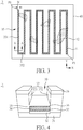
- FIG. 3 shows a top view of the biosensor device 3 according to one embodiment of the present invention. As shown in FIG. 3 , there is a sensing wire 35 extending along a zigzag path in an interface area 40 of the biosensor device 3.
- FIG. 4 shows a perspective view of the structure of the biosensor device 3 according to the present invention.
- FIG. 4 shows a cross-sectional view from A-A line in FIG. 3 .
- the biosensor device 3 includes a substrate 31, a field oxide layer 32, a conductive layer 33, an oxide layer 34, a sensing wire 35, a coating layer 36, a wall layer 37 and a passivation layer 38.
- the substrate 31 can be made of semiconductor materials such as Si, Ge, SiC, GaAs, GaP, InP, InAs, InSb, SiGe, GaAsP, AlInAs, AlGaAs, GaInAs, GaInP, GaInAsP, or the combinations thereof, and it is preferred to be made of Si.
- the field oxide layer 32 is formed on the substrate 31. It can be made of dielectric materials such as silicon oxide, silicon nitride, silicon oxynitride, dielectric with a high dielectric constant (high-k), or the combinations thereof.
- the conductive layer 33 is formed on the field oxide layer 32. It can be made of semiconductor materials as previously described for the substrate 31, and it is preferred to be made of WSi x . Alternatively, the conductive layer 33 can be formed of conductive materials such as Cu, W, Ti, Ta, Cr, Pt, Ag, Au, TiN, TaN, NiSi or CoSi.
- the oxide layer 34 is formed on the conductive layer 33. It can be made of the dielectric materials as previously described for the field oxide layer 32.
- the sensing wire 35 is formed on the oxide layer 34. It can be made of the semiconductor materials as previously described for the substrate 31. In the case of silicon, it can be made of crystalline silicon (c-Si), polycrystalline silicon (poly-Si) and amorphous silicon (a-Si). Furthermore, in this case, the sensing wire 35 is doped with N-type dopants (N+, N or N-) to increase its conductivity. In other cases, it can be doped with P-type dopants (P+, P or P-).
- N-type dopants N+, N or N-
- P-type dopants P+, P or P-
- the sensing wire 35 is connected to a first conducting portion (not shown) at one end and a second conducting portion (not shown) at the other end. Furthermore, the conducting portions are connected to the electrodes, so that the sensing signal generated by the sensing wire 35 can be outputted to an additional circuit (not shown), for example, a comparator, an amplifier or a filter.
- an additional circuit for example, a comparator, an amplifier or a filter.
- the conducting portions can be formed simultaneously with the sensing wire 35, and/or of the same material of the sensing wire 35, and/or at the same layer of the sensing wire 35 on the oxide layer 34.
- Each of the conducting portions has a width larger than the width W (as shown in FIG. 4 ) of the sensing wire 35 for reducing the on-state resistance.
- the coating layer 36 is optionally coated on the sensing wire 35 for capturing (immobilizing) the target biomolecules.
- the coating layer 36 includes organic materials such as proteins, haptens, peptides, polypeptides, antibodies, polynucleotides or crosslinkers, such as chemicals for silanization. In other cases, the coating layer 36 can be omitted.
- the wall layer 37 is formed on the substrate 31, and is covered by the passivation layer 38.
- the wall layer 37 and the passivation layer 38 are etched to form a well 39 until the well 39 reaches the substrate 31.
- the field oxide layer 32, the conductive layer 33, the oxide layer 34, the sensing wire 35, and the coating layer 36 are then formed in turn on the substrate 31 in the well 39.
- the wall layer 37 is substantially formed by a plurality of walls 371 which define the well 39 as well as the path of the sensing wire 35 (as shown in FIG .3 ).
- the wall layer 37 can be a multilayer interconnection (MLI) structure with interlayer dielectric (ILD). Some additional circuits in communication with the biosensor device 3 can be included in the wall layer 37. Those additional circuits may be used to process the sensing signal.
- MMI multilayer interconnection
- ILD interlayer dielectric
- the passivation layer 38 is used to protect the wall layer 37. In some cases, the passivation layer 38 can be omitted.
- the sensing wire 35 is used to receive target biomolecules, such as corpuscles, proteins, carbohydrates, antibodies or metal ions.
- target biomolecules such as corpuscles, proteins, carbohydrates, antibodies or metal ions.
- the target biomolecules will induce an electric field on the sensing wire 35, and the electric field will then induce charges occurring in the sensing wire 35.
- the induced charges will affect resistance of the sensing wire 35. Accordingly, a sensing signal is generated by the sensing wire 35. With the sensing signal, the existence, the amount or the type of target molecules can be determined.
- the interface area 40 is a rectangular area, so that the layout of the biosensor device 3 can be simplified, and the manufacture of the biosensor device 3 can be compatible with the standard CMOS fabrication.
- the sensing wire 35 includes a plurality of first sections 351 extending along a first direction (X-axis direction) and a plurality of second sections 352 extending along a second direction (Y-axis direction).
- the first direction is different from the second direction, namely, they are not parallel to each other. In this case, the first direction is perpendicular to the second direction.
- each of the second sections 352 connects two adjacent ends of two adjacent first sections 351.
- the sensing wire 35 extends continuously in one path without any branch.
- the biosensor device 3 according to the present invention does not require a multiplexer for selection.
- the sensing wire 35 is preferred to extend all over the interface area 40 so as to increase the efficient sensing area. As shown in FIG. 3 , the sensing wire 35 extends at least through the center, the four edges and the four corners of a rectangular interface area 40.
- the sensing wire 35 includes a plurality of first sections 351 extending along a first direction (X-axis direction) and a plurality of second sections 352 extending along a second direction (Y-axis direction), it can extend horizontally to realize a zigzag path.
- the possibility that the sensing wire 35 encounters the defects is sufficiently spread with the zigzag path. Furthermore, since one section that encounters the defects is continuous with one section that avoids the defects, the respective sensing signals will be mixed and then be averaged. Thus, the influence of the defects can be alleviated. It is beneficial to realize a zigzag path for the sensing wire 35 compared to the prior sensor device 1 as shown in FIG. 1 .
- the sensing wire 35 can obtain a better sensing performance if its total length is sufficient long.
- a width W in nanometer-range and a total length L of the sensing wire 35 are defined in FIG. 3 . It is noted that, the total length L starts at P0 at the top-left of the interface area 40, goes along the sensing wire 35, and ends at PI at the bottom-right of the interface area 40.
- the sensing wire 35 can obtain a better sensing performance if the ratio of the total length L to the width W, that is L/W, has certain values.
- the sensing wire 35 has a width W of 50 nm and a total length L of larger than 25 um, and thus L/W is larger than 500.
- the sensing wire 35 has a width W of 50 nm and a total length L of larger than 50 um, and thus L/W is larger than 1000.
- FIGS. 5 to 8 show other embodiments of the biosensor device 3 according to the present invention, which illustrate that several kinds of paths are possible in addition to the zigzag path shown in FIG. 3 .
- FIG. 5 shows a sensing wire 35 extending along a ring-like path.
- the ring-like path goes through the four edges of the interface area 40 for only one round, and the ratio of the total length L (which starts at P0, goes along the sensing wire 35, and ends at PI) of the sensing wire 35 to the width W of the sensing wire 35 is larger than 500. Due to L/W > 500, the sensing wire 35 can still provide a better sensing performance compared to the prior art. A circular path may also be realized if the manufacturing allows.
- FIG. 6 shows a sensing wire 35 extending along a spiral path, which can be regarded as an improvement based on the embodiment of FIG. 5 .
- one end of the sensing wire 35 is at the center of the interface area 40, and the other end the sensing wire 35 is at a corner of the interface area 40, while the ratio of the total length L (which starts at P0, goes along the sensing wire 35, and ends at PI) of the sensing wire 35 to the width W of the sensing wire 35 is larger than 500.
- FIG. 7 shows a sensing wire 35 extending along a symmetrical path.
- the first (left-side) sub-path is symmetrical to the second (right-side) sub-path, and both of them are zigzag paths, and the ratio of the total length L (which starts at P0, goes along the sensing wire 35, and ends at PI) of the sensing wire 35 to the width W of the sensing wire 35 is larger than 500.
- Each of the walls 371 has a width W' equal to the width W of the sensing wire 35.
- FIG. 8 shows a sensing wire 35 extending along a specific path, which includes a plurality of short sections 353 connected to each other, and a plurality of long sections 354 connected to each other.
- the sensing wire 35 starts at one of the short sections 353 and ends at one of the long sections 354, and the ratio of the total length L (which starts at P0, goes along the sensing wire 35, and ends at PI) of the sensing wire 35 to the width W of the sensing wire 35 is larger than 500.
- biosensor device which can reduce the influence of manufacturing variation and improve coefficient of variation in measurements, as well as reduce the complexity and the cost for manufacturing the biosensor device.
Landscapes
- Chemical & Material Sciences (AREA)
- Chemical Kinetics & Catalysis (AREA)
- Electrochemistry (AREA)
- Physics & Mathematics (AREA)
- Health & Medical Sciences (AREA)
- Life Sciences & Earth Sciences (AREA)
- Analytical Chemistry (AREA)
- Biochemistry (AREA)
- General Health & Medical Sciences (AREA)
- General Physics & Mathematics (AREA)
- Immunology (AREA)
- Pathology (AREA)
- Engineering & Computer Science (AREA)
- Nanotechnology (AREA)
- Investigating Or Analyzing Materials By The Use Of Electric Means (AREA)
- Apparatus Associated With Microorganisms And Enzymes (AREA)
Description
- The present invention relates to a biosensor, and more particularly, to a biosensor device.
- Biosensors are expected for measurements in biological features such as corpuscles, proteins, carbohydrates, antibodies or metal ions. Biosensors are advantageous for their high specificity, high sensitivity and high selectivity, and are applicable in the fields of medicine, biological technology, food, agriculture and environment monitoring.
-
FIG. 1 shows aprior sensor device 1, in which asensing wire 11 is used to detect the target biomolecules. However, due to manufacturing tolerances, such as non-uniformity of etching, non-uniformity of coating or non-uniformity of doping, there may be somedefects 12 existing in thesensor device 1. As shown inFIG. 1 , thedefects 12 also exist in a part of thesensing wire 11, which will cause measurement inaccuracy in sensing for thesensor device 1. -
FIG. 2 shows another prior sensor device 2, in which a plurality ofsensing wires 21 are used to detect the target biomolecules, and thus some of thesensing wires 21 can be kept away from thedefects 12. However, in order to receive the sensing signals generated by the sensing wires, amultiplexer 22 is required for selecting the sensing signals to be outputted. Themultiplexer 22 and its wiring will increase the complexity and the cost for manufacturing the sensor device 2. - Inkyu Park et al, "Towards the silicon nanowire-based sensor for intracellular biochemical detection", Biosensors and Bioelectronics, , disclosed a microneedle sensor platform with integrated silicon nanowire tip that was developed for intracellular biochemical detection.
-
US 2006/0006463 A1 disclosed a nano-scale device and method of fabrication provide a nanowire having vertical sidewalls. -
US 2012/0077680 A1 disclosed systems, articles, and methods are provided related to nanowire-based detectors, which can be used for light detection in, for example, single-photon detectors. - Therefore, it is desirable to provide an improved biosensor device to mitigate or obviate the aforementioned problems.
- An object of the present invention is to provide a biosensor device which can reduce the influence of manufacturing variation and improve coefficient of variation in measurements.
- Another object of the present invention is to provide a biosensor device which can reduce the complexity and the cost for manufacturing the biosensor device.
- To achieve the objects, the biosensor device according to the present invention and
independent claim 1 includes a substrate, an oxide layer and a sensing wire. - The oxide layer is disposed (deposited) on the substrate. The sensing wire is disposed (deposited) on the oxide layer. The sensing wire is provided to receive target biomolecules. The sensing wire includes at least one first section extending along a first direction and at least one second section extending along a second direction, the at least one first section is continuous with the at least one second section, and the first direction is different from the second direction. The sensing wire has a width in nanometer-range and a total length, and the ratio of the total length to the width is larger than 500. The sensing wire is disposed in a well surrounded by a wall layer.
- Other objects, advantages, and novel features of the invention will become more apparent from the following detailed description when taken in conjunction with the accompanying drawings.
-
-
FIG. 1 shows a prior sensor device; -
FIG. 2 shows another prior sensor device; -
FIG. 3 shows a top view of the biosensor device according to one embodiment of the present invention; -
FIG. 4 shows a perspective view of the structure of the biosensor device according to the present invention; and -
FIGS. 5 to 8 show top views of the biosensor devices according to other embodiments of the present invention. - Different embodiments according to the present invention are provided in the following description. It is to be understood that the embodiments are not meant to be limiting. Other embodiments can be utilized by arranging, substituting, combining, separating, and designing the features according to the present invention, without departing from the scope of the claims.
-
FIG. 3 shows a top view of thebiosensor device 3 according to one embodiment of the present invention. As shown inFIG. 3 , there is asensing wire 35 extending along a zigzag path in aninterface area 40 of thebiosensor device 3. - To further describe the details of the
biosensor device 3,FIG. 4 shows a perspective view of the structure of thebiosensor device 3 according to the present invention. In particular,FIG. 4 shows a cross-sectional view from A-A line inFIG. 3 . As shown inFIG. 4 , thebiosensor device 3 includes asubstrate 31, afield oxide layer 32, aconductive layer 33, anoxide layer 34, asensing wire 35, acoating layer 36, awall layer 37 and apassivation layer 38. - The
substrate 31 can be made of semiconductor materials such as Si, Ge, SiC, GaAs, GaP, InP, InAs, InSb, SiGe, GaAsP, AlInAs, AlGaAs, GaInAs, GaInP, GaInAsP, or the combinations thereof, and it is preferred to be made of Si. - The
field oxide layer 32 is formed on thesubstrate 31. It can be made of dielectric materials such as silicon oxide, silicon nitride, silicon oxynitride, dielectric with a high dielectric constant (high-k), or the combinations thereof. - The
conductive layer 33 is formed on thefield oxide layer 32. It can be made of semiconductor materials as previously described for thesubstrate 31, and it is preferred to be made of WSix. Alternatively, theconductive layer 33 can be formed of conductive materials such as Cu, W, Ti, Ta, Cr, Pt, Ag, Au, TiN, TaN, NiSi or CoSi. - The
oxide layer 34 is formed on theconductive layer 33. It can be made of the dielectric materials as previously described for thefield oxide layer 32. - The
sensing wire 35 is formed on theoxide layer 34. It can be made of the semiconductor materials as previously described for thesubstrate 31. In the case of silicon, it can be made of crystalline silicon (c-Si), polycrystalline silicon (poly-Si) and amorphous silicon (a-Si). Furthermore, in this case, thesensing wire 35 is doped with N-type dopants (N+, N or N-) to increase its conductivity. In other cases, it can be doped with P-type dopants (P+, P or P-). - In general, the
sensing wire 35 is connected to a first conducting portion (not shown) at one end and a second conducting portion (not shown) at the other end. Furthermore, the conducting portions are connected to the electrodes, so that the sensing signal generated by thesensing wire 35 can be outputted to an additional circuit (not shown), for example, a comparator, an amplifier or a filter. - The conducting portions can be formed simultaneously with the
sensing wire 35, and/or of the same material of thesensing wire 35, and/or at the same layer of thesensing wire 35 on theoxide layer 34. Each of the conducting portions has a width larger than the width W (as shown inFIG. 4 ) of thesensing wire 35 for reducing the on-state resistance. - The
coating layer 36 is optionally coated on thesensing wire 35 for capturing (immobilizing) the target biomolecules. Thecoating layer 36 includes organic materials such as proteins, haptens, peptides, polypeptides, antibodies, polynucleotides or crosslinkers, such as chemicals for silanization. In other cases, thecoating layer 36 can be omitted. - In manufacturing, the
wall layer 37 is formed on thesubstrate 31, and is covered by thepassivation layer 38. Thewall layer 37 and thepassivation layer 38 are etched to form awell 39 until thewell 39 reaches thesubstrate 31. Thefield oxide layer 32, theconductive layer 33, theoxide layer 34, thesensing wire 35, and thecoating layer 36 are then formed in turn on thesubstrate 31 in thewell 39. - It can be seen that the
wall layer 37 is substantially formed by a plurality ofwalls 371 which define the well 39 as well as the path of the sensing wire 35 (as shown inFIG .3 ). - The
wall layer 37 can be a multilayer interconnection (MLI) structure with interlayer dielectric (ILD). Some additional circuits in communication with thebiosensor device 3 can be included in thewall layer 37. Those additional circuits may be used to process the sensing signal. - The
passivation layer 38 is used to protect thewall layer 37. In some cases, thepassivation layer 38 can be omitted. - In operation, the
sensing wire 35 is used to receive target biomolecules, such as corpuscles, proteins, carbohydrates, antibodies or metal ions. The target biomolecules will induce an electric field on thesensing wire 35, and the electric field will then induce charges occurring in thesensing wire 35. The induced charges will affect resistance of thesensing wire 35. Accordingly, a sensing signal is generated by thesensing wire 35. With the sensing signal, the existence, the amount or the type of target molecules can be determined. - Referring back to
FIG. 3 , theinterface area 40 is a rectangular area, so that the layout of thebiosensor device 3 can be simplified, and the manufacture of thebiosensor device 3 can be compatible with the standard CMOS fabrication. - As shown in
FIG. 3 , thesensing wire 35 includes a plurality offirst sections 351 extending along a first direction (X-axis direction) and a plurality ofsecond sections 352 extending along a second direction (Y-axis direction). The first direction is different from the second direction, namely, they are not parallel to each other. In this case, the first direction is perpendicular to the second direction. Further, each of thesecond sections 352 connects two adjacent ends of two adjacentfirst sections 351. - It is noted that, the
sensing wire 35 extends continuously in one path without any branch. Thus, compared to the prior sensor device 2 as shown inFIG. 2 , thebiosensor device 3 according to the present invention does not require a multiplexer for selection. - The
sensing wire 35 is preferred to extend all over theinterface area 40 so as to increase the efficient sensing area. As shown inFIG. 3 , thesensing wire 35 extends at least through the center, the four edges and the four corners of arectangular interface area 40. - Since the
sensing wire 35 includes a plurality offirst sections 351 extending along a first direction (X-axis direction) and a plurality ofsecond sections 352 extending along a second direction (Y-axis direction), it can extend horizontally to realize a zigzag path. - Since the defects can be distributed everywhere with equal possibility, the possibility that the
sensing wire 35 encounters the defects is sufficiently spread with the zigzag path. Furthermore, since one section that encounters the defects is continuous with one section that avoids the defects, the respective sensing signals will be mixed and then be averaged. Thus, the influence of the defects can be alleviated. It is beneficial to realize a zigzag path for thesensing wire 35 compared to theprior sensor device 1 as shown inFIG. 1 . - Besides, the
sensing wire 35 can obtain a better sensing performance if its total length is sufficient long. For quantitative analysis, a width W in nanometer-range and a total length L of thesensing wire 35 are defined inFIG. 3 . It is noted that, the total length L starts at P0 at the top-left of theinterface area 40, goes along thesensing wire 35, and ends at PI at the bottom-right of theinterface area 40. - Based on experimental results, it shows that the
sensing wire 35 can obtain a better sensing performance if the ratio of the total length L to the width W, that is L/W, has certain values. - Preferably, the
sensing wire 35 has a width W of 50 nm and a total length L of larger than 25 um, and thus L/W is larger than 500. Preferably, thesensing wire 35 has a width W of 50 nm and a total length L of larger than 50 um, and thus L/W is larger than 1000. -
FIGS. 5 to 8 show other embodiments of thebiosensor device 3 according to the present invention, which illustrate that several kinds of paths are possible in addition to the zigzag path shown inFIG. 3 . -
FIG. 5 shows asensing wire 35 extending along a ring-like path. The ring-like path goes through the four edges of theinterface area 40 for only one round, and the ratio of the total length L (which starts at P0, goes along thesensing wire 35, and ends at PI) of thesensing wire 35 to the width W of thesensing wire 35 is larger than 500. Due to L/W > 500, thesensing wire 35 can still provide a better sensing performance compared to the prior art. A circular path may also be realized if the manufacturing allows. -
FIG. 6 shows asensing wire 35 extending along a spiral path, which can be regarded as an improvement based on the embodiment ofFIG. 5 . As shown inFIG. 6 , one end of thesensing wire 35 is at the center of theinterface area 40, and the other end thesensing wire 35 is at a corner of theinterface area 40, while the ratio of the total length L (which starts at P0, goes along thesensing wire 35, and ends at PI) of thesensing wire 35 to the width W of thesensing wire 35 is larger than 500. -
FIG. 7 shows asensing wire 35 extending along a symmetrical path. The first (left-side) sub-path is symmetrical to the second (right-side) sub-path, and both of them are zigzag paths, and the ratio of the total length L (which starts at P0, goes along thesensing wire 35, and ends at PI) of thesensing wire 35 to the width W of thesensing wire 35 is larger than 500. Each of thewalls 371 has a width W' equal to the width W of thesensing wire 35. -
FIG. 8 shows asensing wire 35 extending along a specific path, which includes a plurality ofshort sections 353 connected to each other, and a plurality oflong sections 354 connected to each other. Thesensing wire 35 starts at one of theshort sections 353 and ends at one of thelong sections 354, and the ratio of the total length L (which starts at P0, goes along thesensing wire 35, and ends at PI) of thesensing wire 35 to the width W of thesensing wire 35 is larger than 500. - Hence, different embodiments has been provided for implementing a biosensor device which can reduce the influence of manufacturing variation and improve coefficient of variation in measurements, as well as reduce the complexity and the cost for manufacturing the biosensor device.
- Although the present invention has been explained with the aforementioned embodiment, it is to be understood that many other modifications and variations can be made without departing from the scope of the invention as hereinafter claimed.
Claims (13)
- A biosensor device (3), comprising:a substrate (31);an oxide layer (32) disposed on the substrate (31); anda sensing wire (35) disposed on the oxide layer (32) adapted for receiving target biomolecules, and including at least one first section (351) extending along a first direction and at least one second section (352) extending along a second direction, the at least one first section (351) being continuous with the at least one second section (352), the first direction being different from the second direction,characterized in that the sensing wire (35) has a width (W) in nanometer-range and a total length (L) and a ratio (L/W) of the total length (L) to the width (W) is larger than 500; andthe sensing wire (35) is disposed in a well (39) surrounded by a wall layer (37).
- The biosensor device (3) as claimed in claim 1, wherein the first direction is perpendicular to the second direction.
- The biosensor device (3) as claimed in claim 1, wherein the sensing wire (35) extends along one path without any branch.
- The biosensor device (3) as claimed in claim 1, wherein the sensing wire (35) has a plurality of the first sections (351) and a plurality of the second sections (352), and each of the second sections (352) connects two adjacent first sections (351).
- The biosensor device (3) as claimed in claim 1, wherein the sensing wire (35) extends through a center, four edges and four corners of a rectangular interface area (40).
- The biosensor device (3) as claimed in claim 1, wherein the sensing wire (35) extends along a zigzag path.
- The biosensor device (3) as claimed in claim 1, wherein the sensing wire (35) extends along a spiral path.
- The biosensor device (3) as claimed in claim 1, wherein the sensing wire (35) extends along a path with a first sub-path symmetrical to a second sub-path.
- The biosensor device (3) as claimed in claim 1, wherein the sensing wire (35) extends along a zigzag path with a first sub-path symmetrical to a second sub-path.
- The biosensor device (3) as claimed in claim 1, wherein the sensing wire (35) includes a plurality of short sections (353) connected to each other, and a plurality of long sections (354) connected to each other; and the short sections (353) are shorter than the long sections (354).
- The biosensor device (3) as claimed in claim 1, wherein the ratio (L/W) of the width (W) to the total length (L) is 1000.
- The biosensor device (3) as claimed in claim 1, further comprising a coating layer (36) coated on the sensing wire (35), wherein the coating layer (36) is formed of organic materials.
- The biosensor device (3) as claimed in claim 1, further comprising a first conducting portion and a second conducting portion disposed on the oxide layer (34), the first conducting portion being connected to one end of the sensing wire (35), the second conducting portion being connected to the other end of the sensing wire (35), wherein each of the first conducting portion and the second conducting portion has a width larger than the width (W) of the sensing wire (35).
Applications Claiming Priority (1)
| Application Number | Priority Date | Filing Date | Title |
|---|---|---|---|
| TW106100612A TWI635274B (en) | 2017-01-09 | 2017-01-09 | Biosensor device |
Publications (2)
| Publication Number | Publication Date |
|---|---|
| EP3346263A1 EP3346263A1 (en) | 2018-07-11 |
| EP3346263B1 true EP3346263B1 (en) | 2020-08-12 |
Family
ID=60937667
Family Applications (1)
| Application Number | Title | Priority Date | Filing Date |
|---|---|---|---|
| EP18150648.6A Not-in-force EP3346263B1 (en) | 2017-01-09 | 2018-01-08 | Biosensor device |
Country Status (3)
| Country | Link |
|---|---|
| EP (1) | EP3346263B1 (en) |
| CN (1) | CN108287182A (en) |
| TW (1) | TWI635274B (en) |
Family Cites Families (9)
| Publication number | Priority date | Publication date | Assignee | Title |
|---|---|---|---|---|
| US7692179B2 (en) * | 2004-07-09 | 2010-04-06 | Hewlett-Packard Development Company, L.P. | Nanowire device with (111) vertical sidewalls and method of fabrication |
| JP3874772B2 (en) * | 2004-07-21 | 2007-01-31 | 株式会社日立製作所 | Biologically related substance measuring apparatus and measuring method |
| KR20090065124A (en) * | 2007-12-17 | 2009-06-22 | 한국전자통신연구원 | Biosensor using silicon nanowires and its manufacturing method |
| WO2011150321A1 (en) * | 2010-05-28 | 2011-12-01 | Massachusetts Institute Of Technology | Photon detector based on superconducting nanowires |
| CN103842817A (en) * | 2010-09-29 | 2014-06-04 | 得克萨斯系统大学评议会 | Fin-FET biosensor with improved sensitivity and specificity |
| MY163139A (en) * | 2010-12-02 | 2017-08-15 | Mimos Berhad | Resistive ion sensing device |
| CN103592353B (en) * | 2013-11-13 | 2016-05-18 | 胡文闯 | Based on the biology sensor of the linear channel ion sensitive field effect transistor that wriggles |
| CN103901085B (en) * | 2014-04-23 | 2016-05-25 | 中国科学院上海微系统与信息技术研究所 | Biology sensor based on silicon nanowires tunneling field-effect transistor and preparation method |
| CN104730136A (en) * | 2015-03-26 | 2015-06-24 | 中国科学院上海微系统与信息技术研究所 | Biosensor based on germanium nanowire field effect transistor, method and application |
-
2017
- 2017-01-09 TW TW106100612A patent/TWI635274B/en not_active IP Right Cessation
- 2017-09-12 CN CN201710819649.XA patent/CN108287182A/en active Pending
-
2018
- 2018-01-08 EP EP18150648.6A patent/EP3346263B1/en not_active Not-in-force
Non-Patent Citations (1)
| Title |
|---|
| None * |
Also Published As
| Publication number | Publication date |
|---|---|
| CN108287182A (en) | 2018-07-17 |
| TWI635274B (en) | 2018-09-11 |
| EP3346263A1 (en) | 2018-07-11 |
| TW201825892A (en) | 2018-07-16 |
Similar Documents
| Publication | Publication Date | Title |
|---|---|---|
| US10563252B2 (en) | Ultrasensitive biosensors | |
| US11614422B2 (en) | Dual gate biologically sensitive field effect transistor | |
| US10466199B2 (en) | Biosensor device | |
| TWI557409B (en) | Biological field effect transistor, manufacturing method thereof and biochip | |
| US20100176463A1 (en) | Semiconductor device and manufacturing method of the same | |
| US9239309B2 (en) | Humidity sensor and method of manufacturing the same | |
| DE102010028275A1 (en) | Integrated Seebeck differential temperature sensor | |
| US12523716B2 (en) | Compensation circuit and compensation method for magnetic field sensing element | |
| EP2708878B1 (en) | Method of manufacturing an integrated circuit comprising a gas sensor | |
| US20030210507A1 (en) | Temperature sensor for a MOS circuit configuration | |
| US20230375499A1 (en) | Biological Device And Biosensing Method Thereof | |
| US20150061069A1 (en) | Integrating a capacitor in an integrated circuit | |
| KR102921940B1 (en) | Resistance measuring structures of stacked devices | |
| JP2018004345A (en) | Chemical sensor, and method and device for detecting chemical substance | |
| US6512369B2 (en) | Temperature compensated voltage divider with a magnetoresistor and a reference resistor | |
| US10533963B2 (en) | Biosensor device | |
| EP3346263A1 (en) | Biosensor device | |
| CN118483628B (en) | Magnetic sensitive element and preparation method thereof, magnetic sensitive sensor, electronic device, chip and electronic device | |
| CN209446650U (en) | Glass isolator part and its current sensor | |
| US10935516B2 (en) | Ion-sensitive field-effect transistor formed with alternating dielectric stack to enhance sensitivity | |
| EP3325958A1 (en) | Sensor element for a chemical sensor and chemical sensor | |
| US11320395B2 (en) | BioFET and method of manufacturing the same | |
| US12411105B2 (en) | Semiconductor structure with frontside port and cavity features for conveying sample to sensing element | |
| Hellström et al. | Integration of silicon nanowires with CMOS | |
| US11131647B2 (en) | Ion-sensitive field-effect transistor with sawtooth well to enhance sensitivity |
Legal Events
| Date | Code | Title | Description |
|---|---|---|---|
| PUAI | Public reference made under article 153(3) epc to a published international application that has entered the european phase |
Free format text: ORIGINAL CODE: 0009012 |
|
| STAA | Information on the status of an ep patent application or granted ep patent |
Free format text: STATUS: THE APPLICATION HAS BEEN PUBLISHED |
|
| AK | Designated contracting states |
Kind code of ref document: A1 Designated state(s): AL AT BE BG CH CY CZ DE DK EE ES FI FR GB GR HR HU IE IS IT LI LT LU LV MC MK MT NL NO PL PT RO RS SE SI SK SM TR |
|
| AX | Request for extension of the european patent |
Extension state: BA ME |
|
| STAA | Information on the status of an ep patent application or granted ep patent |
Free format text: STATUS: REQUEST FOR EXAMINATION WAS MADE |
|
| 17P | Request for examination filed |
Effective date: 20180925 |
|
| RBV | Designated contracting states (corrected) |
Designated state(s): AL AT BE BG CH CY CZ DE DK EE ES FI FR GB GR HR HU IE IS IT LI LT LU LV MC MK MT NL NO PL PT RO RS SE SI SK SM TR |
|
| STAA | Information on the status of an ep patent application or granted ep patent |
Free format text: STATUS: EXAMINATION IS IN PROGRESS |
|
| 17Q | First examination report despatched |
Effective date: 20191031 |
|
| GRAP | Despatch of communication of intention to grant a patent |
Free format text: ORIGINAL CODE: EPIDOSNIGR1 |
|
| STAA | Information on the status of an ep patent application or granted ep patent |
Free format text: STATUS: GRANT OF PATENT IS INTENDED |
|
| INTG | Intention to grant announced |
Effective date: 20200430 |
|
| RAP1 | Party data changed (applicant data changed or rights of an application transferred) |
Owner name: MOBIOSENSE CORP. |
|
| GRAS | Grant fee paid |
Free format text: ORIGINAL CODE: EPIDOSNIGR3 |
|
| GRAA | (expected) grant |
Free format text: ORIGINAL CODE: 0009210 |
|
| STAA | Information on the status of an ep patent application or granted ep patent |
Free format text: STATUS: THE PATENT HAS BEEN GRANTED |
|
| AK | Designated contracting states |
Kind code of ref document: B1 Designated state(s): AL AT BE BG CH CY CZ DE DK EE ES FI FR GB GR HR HU IE IS IT LI LT LU LV MC MK MT NL NO PL PT RO RS SE SI SK SM TR |
|
| REG | Reference to a national code |
Ref country code: CH Ref legal event code: EP |
|
| REG | Reference to a national code |
Ref country code: IE Ref legal event code: FG4D |
|
| REG | Reference to a national code |
Ref country code: DE Ref legal event code: R096 Ref document number: 602018006742 Country of ref document: DE |
|
| REG | Reference to a national code |
Ref country code: AT Ref legal event code: REF Ref document number: 1302034 Country of ref document: AT Kind code of ref document: T Effective date: 20200915 |
|
| REG | Reference to a national code |
Ref country code: LT Ref legal event code: MG4D |
|
| REG | Reference to a national code |
Ref country code: NL Ref legal event code: MP Effective date: 20200812 |
|
| PG25 | Lapsed in a contracting state [announced via postgrant information from national office to epo] |
Ref country code: LT Free format text: LAPSE BECAUSE OF FAILURE TO SUBMIT A TRANSLATION OF THE DESCRIPTION OR TO PAY THE FEE WITHIN THE PRESCRIBED TIME-LIMIT Effective date: 20200812 Ref country code: NO Free format text: LAPSE BECAUSE OF FAILURE TO SUBMIT A TRANSLATION OF THE DESCRIPTION OR TO PAY THE FEE WITHIN THE PRESCRIBED TIME-LIMIT Effective date: 20201112 Ref country code: GR Free format text: LAPSE BECAUSE OF FAILURE TO SUBMIT A TRANSLATION OF THE DESCRIPTION OR TO PAY THE FEE WITHIN THE PRESCRIBED TIME-LIMIT Effective date: 20201113 Ref country code: SE Free format text: LAPSE BECAUSE OF FAILURE TO SUBMIT A TRANSLATION OF THE DESCRIPTION OR TO PAY THE FEE WITHIN THE PRESCRIBED TIME-LIMIT Effective date: 20200812 Ref country code: HR Free format text: LAPSE BECAUSE OF FAILURE TO SUBMIT A TRANSLATION OF THE DESCRIPTION OR TO PAY THE FEE WITHIN THE PRESCRIBED TIME-LIMIT Effective date: 20200812 Ref country code: FI Free format text: LAPSE BECAUSE OF FAILURE TO SUBMIT A TRANSLATION OF THE DESCRIPTION OR TO PAY THE FEE WITHIN THE PRESCRIBED TIME-LIMIT Effective date: 20200812 Ref country code: BG Free format text: LAPSE BECAUSE OF FAILURE TO SUBMIT A TRANSLATION OF THE DESCRIPTION OR TO PAY THE FEE WITHIN THE PRESCRIBED TIME-LIMIT Effective date: 20201112 |
|
| REG | Reference to a national code |
Ref country code: AT Ref legal event code: MK05 Ref document number: 1302034 Country of ref document: AT Kind code of ref document: T Effective date: 20200812 |
|
| PG25 | Lapsed in a contracting state [announced via postgrant information from national office to epo] |
Ref country code: IS Free format text: LAPSE BECAUSE OF FAILURE TO SUBMIT A TRANSLATION OF THE DESCRIPTION OR TO PAY THE FEE WITHIN THE PRESCRIBED TIME-LIMIT Effective date: 20201212 Ref country code: NL Free format text: LAPSE BECAUSE OF FAILURE TO SUBMIT A TRANSLATION OF THE DESCRIPTION OR TO PAY THE FEE WITHIN THE PRESCRIBED TIME-LIMIT Effective date: 20200812 Ref country code: PL Free format text: LAPSE BECAUSE OF FAILURE TO SUBMIT A TRANSLATION OF THE DESCRIPTION OR TO PAY THE FEE WITHIN THE PRESCRIBED TIME-LIMIT Effective date: 20200812 Ref country code: RS Free format text: LAPSE BECAUSE OF FAILURE TO SUBMIT A TRANSLATION OF THE DESCRIPTION OR TO PAY THE FEE WITHIN THE PRESCRIBED TIME-LIMIT Effective date: 20200812 Ref country code: LV Free format text: LAPSE BECAUSE OF FAILURE TO SUBMIT A TRANSLATION OF THE DESCRIPTION OR TO PAY THE FEE WITHIN THE PRESCRIBED TIME-LIMIT Effective date: 20200812 |
|
| PG25 | Lapsed in a contracting state [announced via postgrant information from national office to epo] |
Ref country code: DK Free format text: LAPSE BECAUSE OF FAILURE TO SUBMIT A TRANSLATION OF THE DESCRIPTION OR TO PAY THE FEE WITHIN THE PRESCRIBED TIME-LIMIT Effective date: 20200812 Ref country code: CZ Free format text: LAPSE BECAUSE OF FAILURE TO SUBMIT A TRANSLATION OF THE DESCRIPTION OR TO PAY THE FEE WITHIN THE PRESCRIBED TIME-LIMIT Effective date: 20200812 Ref country code: RO Free format text: LAPSE BECAUSE OF FAILURE TO SUBMIT A TRANSLATION OF THE DESCRIPTION OR TO PAY THE FEE WITHIN THE PRESCRIBED TIME-LIMIT Effective date: 20200812 Ref country code: EE Free format text: LAPSE BECAUSE OF FAILURE TO SUBMIT A TRANSLATION OF THE DESCRIPTION OR TO PAY THE FEE WITHIN THE PRESCRIBED TIME-LIMIT Effective date: 20200812 Ref country code: SM Free format text: LAPSE BECAUSE OF FAILURE TO SUBMIT A TRANSLATION OF THE DESCRIPTION OR TO PAY THE FEE WITHIN THE PRESCRIBED TIME-LIMIT Effective date: 20200812 |
|
| REG | Reference to a national code |
Ref country code: DE Ref legal event code: R097 Ref document number: 602018006742 Country of ref document: DE |
|
| PG25 | Lapsed in a contracting state [announced via postgrant information from national office to epo] |
Ref country code: ES Free format text: LAPSE BECAUSE OF FAILURE TO SUBMIT A TRANSLATION OF THE DESCRIPTION OR TO PAY THE FEE WITHIN THE PRESCRIBED TIME-LIMIT Effective date: 20200812 Ref country code: AT Free format text: LAPSE BECAUSE OF FAILURE TO SUBMIT A TRANSLATION OF THE DESCRIPTION OR TO PAY THE FEE WITHIN THE PRESCRIBED TIME-LIMIT Effective date: 20200812 Ref country code: AL Free format text: LAPSE BECAUSE OF FAILURE TO SUBMIT A TRANSLATION OF THE DESCRIPTION OR TO PAY THE FEE WITHIN THE PRESCRIBED TIME-LIMIT Effective date: 20200812 |
|
| PLBE | No opposition filed within time limit |
Free format text: ORIGINAL CODE: 0009261 |
|
| STAA | Information on the status of an ep patent application or granted ep patent |
Free format text: STATUS: NO OPPOSITION FILED WITHIN TIME LIMIT |
|
| PG25 | Lapsed in a contracting state [announced via postgrant information from national office to epo] |
Ref country code: SK Free format text: LAPSE BECAUSE OF FAILURE TO SUBMIT A TRANSLATION OF THE DESCRIPTION OR TO PAY THE FEE WITHIN THE PRESCRIBED TIME-LIMIT Effective date: 20200812 |
|
| 26N | No opposition filed |
Effective date: 20210514 |
|
| PG25 | Lapsed in a contracting state [announced via postgrant information from national office to epo] |
Ref country code: IT Free format text: LAPSE BECAUSE OF FAILURE TO SUBMIT A TRANSLATION OF THE DESCRIPTION OR TO PAY THE FEE WITHIN THE PRESCRIBED TIME-LIMIT Effective date: 20200812 |
|
| PG25 | Lapsed in a contracting state [announced via postgrant information from national office to epo] |
Ref country code: SI Free format text: LAPSE BECAUSE OF FAILURE TO SUBMIT A TRANSLATION OF THE DESCRIPTION OR TO PAY THE FEE WITHIN THE PRESCRIBED TIME-LIMIT Effective date: 20200812 Ref country code: MC Free format text: LAPSE BECAUSE OF FAILURE TO SUBMIT A TRANSLATION OF THE DESCRIPTION OR TO PAY THE FEE WITHIN THE PRESCRIBED TIME-LIMIT Effective date: 20200812 |
|
| REG | Reference to a national code |
Ref country code: CH Ref legal event code: PL |
|
| PG25 | Lapsed in a contracting state [announced via postgrant information from national office to epo] |
Ref country code: LU Free format text: LAPSE BECAUSE OF NON-PAYMENT OF DUE FEES Effective date: 20210108 |
|
| REG | Reference to a national code |
Ref country code: BE Ref legal event code: MM Effective date: 20210131 |
|
| PG25 | Lapsed in a contracting state [announced via postgrant information from national office to epo] |
Ref country code: CH Free format text: LAPSE BECAUSE OF NON-PAYMENT OF DUE FEES Effective date: 20210131 Ref country code: LI Free format text: LAPSE BECAUSE OF NON-PAYMENT OF DUE FEES Effective date: 20210131 |
|
| PG25 | Lapsed in a contracting state [announced via postgrant information from national office to epo] |
Ref country code: IE Free format text: LAPSE BECAUSE OF NON-PAYMENT OF DUE FEES Effective date: 20210108 |
|
| PGFP | Annual fee paid to national office [announced via postgrant information from national office to epo] |
Ref country code: FR Payment date: 20211129 Year of fee payment: 5 Ref country code: GB Payment date: 20211126 Year of fee payment: 5 |
|
| PGFP | Annual fee paid to national office [announced via postgrant information from national office to epo] |
Ref country code: DE Payment date: 20211129 Year of fee payment: 5 |
|
| PG25 | Lapsed in a contracting state [announced via postgrant information from national office to epo] |
Ref country code: BE Free format text: LAPSE BECAUSE OF NON-PAYMENT OF DUE FEES Effective date: 20210131 |
|
| PG25 | Lapsed in a contracting state [announced via postgrant information from national office to epo] |
Ref country code: PT Free format text: LAPSE BECAUSE OF FAILURE TO SUBMIT A TRANSLATION OF THE DESCRIPTION OR TO PAY THE FEE WITHIN THE PRESCRIBED TIME-LIMIT Effective date: 20201214 |
|
| PG25 | Lapsed in a contracting state [announced via postgrant information from national office to epo] |
Ref country code: CY Free format text: LAPSE BECAUSE OF FAILURE TO SUBMIT A TRANSLATION OF THE DESCRIPTION OR TO PAY THE FEE WITHIN THE PRESCRIBED TIME-LIMIT Effective date: 20200812 |
|
| PG25 | Lapsed in a contracting state [announced via postgrant information from national office to epo] |
Ref country code: HU Free format text: LAPSE BECAUSE OF FAILURE TO SUBMIT A TRANSLATION OF THE DESCRIPTION OR TO PAY THE FEE WITHIN THE PRESCRIBED TIME-LIMIT; INVALID AB INITIO Effective date: 20180108 |
|
| REG | Reference to a national code |
Ref country code: DE Ref legal event code: R119 Ref document number: 602018006742 Country of ref document: DE |
|
| GBPC | Gb: european patent ceased through non-payment of renewal fee |
Effective date: 20230108 |
|
| PG25 | Lapsed in a contracting state [announced via postgrant information from national office to epo] |
Ref country code: GB Free format text: LAPSE BECAUSE OF NON-PAYMENT OF DUE FEES Effective date: 20230108 Ref country code: DE Free format text: LAPSE BECAUSE OF NON-PAYMENT OF DUE FEES Effective date: 20230801 |
|
| PG25 | Lapsed in a contracting state [announced via postgrant information from national office to epo] |
Ref country code: FR Free format text: LAPSE BECAUSE OF NON-PAYMENT OF DUE FEES Effective date: 20230131 |
|
| PG25 | Lapsed in a contracting state [announced via postgrant information from national office to epo] |
Ref country code: MK Free format text: LAPSE BECAUSE OF FAILURE TO SUBMIT A TRANSLATION OF THE DESCRIPTION OR TO PAY THE FEE WITHIN THE PRESCRIBED TIME-LIMIT Effective date: 20200812 |
|
| PG25 | Lapsed in a contracting state [announced via postgrant information from national office to epo] |
Ref country code: MT Free format text: LAPSE BECAUSE OF FAILURE TO SUBMIT A TRANSLATION OF THE DESCRIPTION OR TO PAY THE FEE WITHIN THE PRESCRIBED TIME-LIMIT Effective date: 20200812 |
|
| PG25 | Lapsed in a contracting state [announced via postgrant information from national office to epo] |
Ref country code: TR Free format text: LAPSE BECAUSE OF FAILURE TO SUBMIT A TRANSLATION OF THE DESCRIPTION OR TO PAY THE FEE WITHIN THE PRESCRIBED TIME-LIMIT Effective date: 20200812 |