EP3345053B1 - A method for manufacturing a membrane assembly - Google Patents
A method for manufacturing a membrane assembly Download PDFInfo
- Publication number
- EP3345053B1 EP3345053B1 EP16757252.8A EP16757252A EP3345053B1 EP 3345053 B1 EP3345053 B1 EP 3345053B1 EP 16757252 A EP16757252 A EP 16757252A EP 3345053 B1 EP3345053 B1 EP 3345053B1
- Authority
- EP
- European Patent Office
- Prior art keywords
- membrane
- layer
- planar substrate
- stack
- border
- Prior art date
- Legal status (The legal status is an assumption and is not a legal conclusion. Google has not performed a legal analysis and makes no representation as to the accuracy of the status listed.)
- Active
Links
Images







Classifications
-
- G—PHYSICS
- G03—PHOTOGRAPHY; CINEMATOGRAPHY; ANALOGOUS TECHNIQUES USING WAVES OTHER THAN OPTICAL WAVES; ELECTROGRAPHY; HOLOGRAPHY
- G03F—PHOTOMECHANICAL PRODUCTION OF TEXTURED OR PATTERNED SURFACES, e.g. FOR PRINTING, FOR PROCESSING OF SEMICONDUCTOR DEVICES; MATERIALS THEREFOR; ORIGINALS THEREFOR; APPARATUS SPECIALLY ADAPTED THEREFOR
- G03F1/00—Originals for photomechanical production of textured or patterned surfaces, e.g., masks, photo-masks, reticles; Mask blanks or pellicles therefor; Containers specially adapted therefor; Preparation thereof
- G03F1/62—Pellicles, e.g. pellicle assemblies, e.g. having membrane on support frame; Preparation thereof
-
- G—PHYSICS
- G03—PHOTOGRAPHY; CINEMATOGRAPHY; ANALOGOUS TECHNIQUES USING WAVES OTHER THAN OPTICAL WAVES; ELECTROGRAPHY; HOLOGRAPHY
- G03F—PHOTOMECHANICAL PRODUCTION OF TEXTURED OR PATTERNED SURFACES, e.g. FOR PRINTING, FOR PROCESSING OF SEMICONDUCTOR DEVICES; MATERIALS THEREFOR; ORIGINALS THEREFOR; APPARATUS SPECIALLY ADAPTED THEREFOR
- G03F1/00—Originals for photomechanical production of textured or patterned surfaces, e.g., masks, photo-masks, reticles; Mask blanks or pellicles therefor; Containers specially adapted therefor; Preparation thereof
- G03F1/68—Preparation processes not covered by groups G03F1/20 - G03F1/50
- G03F1/80—Etching
-
- G—PHYSICS
- G03—PHOTOGRAPHY; CINEMATOGRAPHY; ANALOGOUS TECHNIQUES USING WAVES OTHER THAN OPTICAL WAVES; ELECTROGRAPHY; HOLOGRAPHY
- G03F—PHOTOMECHANICAL PRODUCTION OF TEXTURED OR PATTERNED SURFACES, e.g. FOR PRINTING, FOR PROCESSING OF SEMICONDUCTOR DEVICES; MATERIALS THEREFOR; ORIGINALS THEREFOR; APPARATUS SPECIALLY ADAPTED THEREFOR
- G03F7/00—Photomechanical, e.g. photolithographic, production of textured or patterned surfaces, e.g. printing surfaces; Materials therefor, e.g. comprising photoresists; Apparatus specially adapted therefor
- G03F7/70—Microphotolithographic exposure; Apparatus therefor
- G03F7/70008—Production of exposure light, i.e. light sources
- G03F7/70033—Production of exposure light, i.e. light sources by plasma extreme ultraviolet [EUV] sources
-
- G—PHYSICS
- G03—PHOTOGRAPHY; CINEMATOGRAPHY; ANALOGOUS TECHNIQUES USING WAVES OTHER THAN OPTICAL WAVES; ELECTROGRAPHY; HOLOGRAPHY
- G03F—PHOTOMECHANICAL PRODUCTION OF TEXTURED OR PATTERNED SURFACES, e.g. FOR PRINTING, FOR PROCESSING OF SEMICONDUCTOR DEVICES; MATERIALS THEREFOR; ORIGINALS THEREFOR; APPARATUS SPECIALLY ADAPTED THEREFOR
- G03F7/00—Photomechanical, e.g. photolithographic, production of textured or patterned surfaces, e.g. printing surfaces; Materials therefor, e.g. comprising photoresists; Apparatus specially adapted therefor
- G03F7/70—Microphotolithographic exposure; Apparatus therefor
- G03F7/708—Construction of apparatus, e.g. environment aspects, hygiene aspects or materials
- G03F7/70983—Optical system protection, e.g. pellicles or removable covers for protection of mask
-
- H—ELECTRICITY
- H10—SEMICONDUCTOR DEVICES; ELECTRIC SOLID-STATE DEVICES NOT OTHERWISE PROVIDED FOR
- H10P—GENERIC PROCESSES OR APPARATUS FOR THE MANUFACTURE OR TREATMENT OF DEVICES COVERED BY CLASS H10
- H10P50/00—Etching of wafers, substrates or parts of devices
- H10P50/20—Dry etching; Plasma etching; Reactive-ion etching
- H10P50/24—Dry etching; Plasma etching; Reactive-ion etching of semiconductor materials
- H10P50/242—Dry etching; Plasma etching; Reactive-ion etching of semiconductor materials of Group IV materials
-
- H—ELECTRICITY
- H10—SEMICONDUCTOR DEVICES; ELECTRIC SOLID-STATE DEVICES NOT OTHERWISE PROVIDED FOR
- H10P—GENERIC PROCESSES OR APPARATUS FOR THE MANUFACTURE OR TREATMENT OF DEVICES COVERED BY CLASS H10
- H10P76/00—Manufacture or treatment of masks on semiconductor bodies, e.g. by lithography or photolithography
Definitions
- the present invention relates to a method for manufacturing a membrane assembly, and to a membrane assembly.
- a lithographic apparatus is a machine that applies a desired pattern onto a substrate, usually onto a target portion of the substrate.
- a lithographic apparatus can be used, for example, in the manufacture of integrated circuits (ICs).
- a patterning device which is alternatively referred to as a mask or a reticle, may be used to generate a circuit pattern to be formed on an individual layer of the IC.
- This pattern can be transferred onto a target portion (e.g., comprising part of, one, or several dies) on a substrate (e.g., a silicon wafer). Transfer of the pattern is typically via imaging onto a layer of radiation-sensitive material (resist) provided on the substrate.
- a single substrate will contain a network of adjacent target portions that are successively patterned.
- Lithography is widely recognized as one of the key steps in the manufacture of ICs and other devices and/or structures. However, as the dimensions of features made using lithography become smaller, lithography is becoming a more critical factor for enabling miniature IC or other devices and/or structures to be manufactured.
- CD k 1 ⁇ ⁇ NA
- ⁇ is the wavelength of the radiation used
- NA is the numerical aperture of the projection system used to print the pattern
- k1 is a process-dependent adjustment factor, also called the Rayleigh constant
- CD is the feature size (or critical dimension) of the printed feature. It follows from equation (1) that reduction of the minimum printable size of features can be obtained in three ways: by shortening the exposure wavelength ⁇ , by increasing the numerical aperture NA or by decreasing the value of kl.
- EUV radiation is electromagnetic radiation having a wavelength within the range of 10-20 nm, for example within the range of 13-14 nm. It has further been proposed that EUV radiation with a wavelength of less than 10 nm could be used, for example within the range of 5-10 nm such as 6.7 nm or 6.8 nm. Such radiation is termed extreme ultraviolet radiation or soft x-ray radiation. Possible sources include, for example, laser-produced plasma sources, discharge plasma sources, or sources based on synchrotron radiation provided by an electron storage ring.
- a lithographic apparatus includes a patterning device (e.g., a mask or a reticle). Radiation is provided through or reflected off the patterning device to form an image on a substrate.
- a membrane assembly may be provided to protect the patterning device from airborne particles and other forms of contamination.
- the membrane assembly for protecting the patterning device may be called a pellicle. Contamination on the surface of the patterning device can cause manufacturing defects on the substrate.
- the membrane assembly may comprise a border and a membrane stretched across the border. It is difficult to manufacture the membrane assembly without the membrane assembly being deformed in the process, for example because of the thickness of the membrane.
- the membrane assembly It is also difficult to manufacture the membrane assembly without the membrane assembly being damaged or contaminated in the process.
- the membrane may be undesirably oxidized or have unwanted contaminant particles deposited on the membrane during the process of manufacturing the membrane assembly.
- US 6623893 B1 describes a pellicle comprising a silicon film under tensile stress, an anti-reflective coating and a substrate coupled to the periphery of the film.
- EP 2423747 A1 describes a pellicle comprising a film of single crystal silicon supported by a porous portion and an outer frame portion.
- a method for manufacturing a membrane assembly for EUV lithography comprising: providing a stack comprising a planar substrate and at least one membrane layer, wherein the planar substrate comprises an inner region, a border region around the inner region, a bridge region around the border region and an edge region around the bridge region; forming a bridge groove through the at least one membrane layer adjacent the bridge region of the planar substrate; selectively removing the inner region and the bridge region of the planar substrate, such that the membrane assembly comprises: a membrane formed from the at least one membrane layer; a border holding the membrane, the border formed from the border region of the planar substrate; an edge section around the border, the edge section formed from the edge region of the planar substrate; and a bridge between the border and the edge section, the bridge formed by the at least one membrane layer; and separating the edge section from the border such that the at least one membrane layer adjacent the edge section is separated from the membrane by the bridge groove.
- a membrane assembly for EUV lithography comprising a membrane formed from at least one membrane layer comprising silicon and a border holding the membrane, wherein the edges of the at least one membrane layer are oxidized or nitrided
- Figure 1 schematically depicts a lithographic apparatus 100 including a source collector module SO.
- the apparatus 100 comprises
- the illumination system IL may include various types of optical components, such as refractive, reflective, magnetic, electromagnetic, electrostatic or other types of optical components, or any combination thereof, for directing, shaping, or controlling radiation.
- optical components such as refractive, reflective, magnetic, electromagnetic, electrostatic or other types of optical components, or any combination thereof, for directing, shaping, or controlling radiation.
- the support structure MT holds the patterning device MA in a manner that depends on the orientation of the patterning device, the design of the lithographic apparatus, and other conditions, such as for example whether or not the patterning device is held in a vacuum environment.
- the support structure MT can use mechanical, vacuum, electrostatic or other clamping techniques to hold the patterning device MA.
- the support structure MT may be a frame or a table, for example, which may be fixed or movable as required.
- the support structure MT may ensure that the patterning device MA is at a desired position, for example with respect to the projection system PS.
- patterning device should be broadly interpreted as referring to any device that can be used to impart a radiation beam B with a pattern in its cross-section such as to create a pattern in a target portion C of the substrate W.
- the pattern imparted to the radiation beam B may correspond to a particular functional layer in a device being created in the target portion C, such as an integrated circuit.
- the patterning device MA may be transmissive or reflective.
- Examples of patterning devices include masks, programmable mirror arrays, and programmable liquid-crystal display (LCD) panels.
- Masks are well known in lithography, and include mask types such as binary, alternating phase-shift, and attenuated phase-shift, as well as various hybrid mask types.
- An example of a programmable mirror array employs a matrix arrangement of small mirrors, each of which can be individually tilted so as to reflect an incoming radiation beam in different directions. The tilted mirrors impart a pattern in a radiation beam, which is reflected by the mirror matrix.
- the projection system PS may include various types of optical components, such as refractive, reflective, magnetic, electromagnetic, electrostatic or other types of optical components, or any combination thereof, as appropriate for the exposure radiation being used, or for other factors such as the use of a vacuum. It may be desired to use a vacuum for EUV radiation since other gases may absorb too much radiation. A vacuum environment may therefore be provided to the whole beam path with the aid of a vacuum wall and vacuum pumps.
- the lithographic apparatus 100 is of a reflective type (e.g., employing a reflective mask).
- the lithographic apparatus 100 may be of a type having two (dual stage) or more substrate tables WT (and/or two or more support structures MT).
- the additional substrate tables WT (and/or the additional support structures MT) may be used in parallel, or preparatory steps may be carried out on one or more substrate tables WT (and/or one or more support structures MT) while one or more other substrate tables WT (and/or one or more other support structures MT) are being used for exposure.
- the illumination system IL receives an extreme ultraviolet radiation beam from the source collector module SO.
- Methods to produce EUV light include, but are not necessarily limited to, converting a material into a plasma state that has at least one element, e.g., xenon, lithium or tin, with one or more emission lines in the EUV range.
- LPP laser produced plasma
- the required plasma can be produced by irradiating a fuel, such as a droplet, stream or cluster of material having the required line-emitting element, with a laser beam.
- the source collector module SO may be part of an EUV radiation system including a laser, not shown in Figure 1 , for providing the laser beam exciting the fuel.
- the resulting plasma emits output radiation, e.g., EUV radiation, which is collected using a radiation collector, disposed in the source collector module.
- output radiation e.g., EUV radiation
- the laser and the source collector module SO may be separate entities, for example when a CO 2 laser is used to provide the laser beam for fuel excitation.
- the laser is not considered to form part of the lithographic apparatus 100 and the radiation beam B is passed from the laser to the source collector module SO with the aid of a beam delivery system comprising, for example, suitable directing mirrors and/or a beam expander.
- the source may be an integral part of the source collector module SO, for example when the source is a discharge produced plasma EUV generator, often termed as a DPP source.
- the illumination system IL may comprise an adjuster for adjusting the angular intensity distribution of the radiation beam. Generally, at least the outer and/or inner radial extent (commonly referred to as ⁇ -outer and ⁇ -inner, respectively) of the intensity distribution in a pupil plane of the illumination system IL can be adjusted.
- the illumination system IL may comprise various other components, such as facetted field and pupil mirror devices.
- the illumination system IL may be used to condition the radiation beam B, to have a desired uniformity and intensity distribution in its cross-section.
- the radiation beam B is incident on the patterning device (e.g., mask) MA, which is held on the support structure (e.g., mask table) MT, and is patterned by the patterning device MA.
- the radiation beam B After being reflected from the patterning device (e.g., mask) MA, the radiation beam B passes through the projection system PS, which focuses the radiation beam B onto a target portion C of the substrate W.
- the substrate table WT can be moved accurately, e.g., so as to position different target portions C in the path of the radiation beam B.
- the first positioner PM and another position sensor PS1 can be used to accurately position the patterning device (e.g., mask) MA with respect to the path of the radiation beam B.
- the patterning device (e.g., mask) MA and the substrate W may be aligned using mask alignment marks M1, M2 and substrate alignment marks PI, P2.
- a controller 500 controls the overall operations of the lithographic apparatus 100 and in particular performs an operation process described further below.
- Controller 500 can be embodied as a suitably-programmed general purpose computer comprising a central processing unit, volatile and non-volatile storage means, one or more input and output devices such as a keyboard and screen, one or more network connections and one or more interfaces to the various parts of the lithographic apparatus 100. It will be appreciated that a one-to-one relationship between controlling computer and lithographic apparatus 100 is not necessary.
- one computer can control multiple lithographic apparatuses 100.
- multiple networked computers can be used to control one lithographic apparatus 100.
- the controller 500 may also be configured to control one or more associated process devices and substrate handling devices in a lithocell or cluster of which the lithographic apparatus 100 forms a part.
- the controller 500 can also be configured to be subordinate to a supervisory control system of a lithocell or cluster and/or an overall control system of a fab.
- FIG. 2 shows the lithographic apparatus 100 in more detail, including the source collector module SO, the illumination system IL, and the projection system PS.
- An EUV radiation emitting plasma 210 may be formed by a plasma source. EUV radiation may be produced by a gas or vapor, for example Xe gas, Li vapor or Sn vapor in which the radiation emitting plasma 210 is created to emit radiation in the EUV range of the electromagnetic spectrum. In an embodiment, a plasma of excited tin (Sn) is provided to produce EUV radiation.
- Sn excited tin
- the radiation emitted by the radiation emitting plasma 210 is passed from a source chamber 211 into a collector chamber 212.
- the collector chamber 212 may include a radiation collector CO. Radiation that traverses the radiation collector CO can be focused in a virtual source point IF.
- the virtual source point IF is commonly referred to as the intermediate focus, and the source collector module SO is arranged such that the virtual source point IF is located at or near an opening 221 in the enclosing structure 220.
- the virtual source point IF is an image of the radiation emitting plasma 210.
- the radiation traverses the illumination system IL, which may include a facetted field mirror device 22 and a facetted pupil mirror device 24 arranged to provide a desired angular distribution of the unpatterned beam 21, at the patterning device MA, as well as a desired uniformity of radiation intensity at the patterning device MA.
- the illumination system IL may include a facetted field mirror device 22 and a facetted pupil mirror device 24 arranged to provide a desired angular distribution of the unpatterned beam 21, at the patterning device MA, as well as a desired uniformity of radiation intensity at the patterning device MA.
- More elements than shown may generally be present in the illumination system IL and the projection system PS. Further, there may be more mirrors present than those shown in the Figures, for example there may be 1- 6 additional reflective elements present in the projection system PS than shown in Figure 2 .
- the source collector module SO may be part of an LPP radiation system.
- the lithographic apparatus 100 comprises an illumination system IL and a projection system PS.
- the illumination system IL is configured to emit a radiation beam B.
- the projection system PS is separated from the substrate table WT by an intervening space.
- the projection system PS is configured to project a pattern imparted to the radiation beam B onto the substrate W. The pattern is for EUV radiation of the radiation beam B.
- the space intervening between the projection system PS and the substrate table WT can be at least partially evacuated.
- the intervening space may be delimited at the location of the projection system PS by a solid surface from which the employed radiation is directed toward the substrate table WT.
- the lithographic apparatus 100 comprises a dynamic gas lock.
- the dynamic gas lock comprises a membrane assembly 80.
- the dynamic gas lock comprises a hollow part covered by a membrane assembly 80 located in the intervening space.
- the hollow part is situated around the path of the radiation.
- the lithographic apparatus 100 comprises a gas blower configured to flush the inside of the hollow part with a flow of gas. The radiation travels through the membrane assembly before impinging on the substrate W.
- the lithographic apparatus 100 comprises a membrane assembly 80.
- the membrane assembly 80 is for a dynamic gas lock.
- the membrane assembly 80 functions as a filter for filtering DUV radiation.
- the membrane assembly 80 is pellicle for the patterning device MA for EUV lithography.
- the membrane assembly 80 of the present invention can be used for a dynamic gas lock or for a pellicle or for another purpose.
- the membrane assembly 80 comprises a membrane layer 50 configured to transmit at least 80% of incident EUV radiation.
- the pellicle is configured to seal off the patterning device MA to protect the patterning device MA from airborne particles and other forms of contamination. Contamination on the surface of the patterning device MA can cause manufacturing defects on the substrate W.
- the pellicle is configured to reduce the likelihood that particles might migrate into a stepping field of the patterning device MA in the lithographic apparatus 100.
- the contamination can require the patterning device MA to be cleaned or discarded. Cleaning the patterning device MA interrupts valuable manufacturing time and discarding the patterning device MA is costly. Replacing the patterning device MA also interrupts valuable manufacturing time.
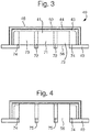
- Figures 3 and 4 schematically depict stages of a method for manufacturing the membrane assembly 80 according to an embodiment of the invention.
- the method for manufacturing the membrane assembly 80 comprises providing a stack 40.
- the stack comprises a planar substrate 41.
- planar substrate 41 is formed from silicon. However the planar substrate 41 may also be formed from a glass/SiO 2 wafer or a SOI wafer.
- the planar substrate 41 has a shape such as a square, a circle or a rectangle, for example. The shape of the planar substrate 41 is not particularly limited.
- the size of the planar substrate 41 is not particularly limited.
- the planar substrate 41 has a diameter in the range of from about 100 mm to about 500 mm, for example about 200 mm.
- the thickness of the planar substrate 41 is not particularly limited.
- the planar substrate 41 has a thickness of at least 100 ⁇ m (e.g. a pre-thinned wafer), for example at least 300 ⁇ m, optionally at least 400 ⁇ m.
- the planar substrate 41 has a thickness of at most 1,000 ⁇ m, optionally at most 800 ⁇ m.
- the planar substrate 41 has a thickness of about 725 ⁇ m.
- the planar substrate 41 has a thickness of at most 600 ⁇ m, optionally at most 400 ⁇ m.
- the amount of the planar substrate 41 that needs to be selectively removed is reduced. Accordingly, by starting with a thinner planar substrate 41, an embodiment of the invention is expected to reduce the possibility of the membrane being damaged or contaminated during the step of selectively removing parts of the planar substrate 41. Additionally, by starting with a planar substrate 41, an embodiment of the invention is expected to make the manufacturing process more efficient.
- Silicon can crystallise in a diamond cubic crystal structure.
- the planar substrate 41 comprises a cubic crystal of silicon.
- the planar substrate 41 has a ⁇ 100> crystallographic direction.
- the method for manufacturing the membrane assembly 80 comprises a step of etching the planar substrate 41.
- Part of the planar substrate 41 forms a border region 72 of the membrane assembly 80, the border region 72 forming a border 75.
- the border 75 holds the membrane of the membrane assembly 80.
- An embodiment of the invention is expected to achieve increased mechanical strength of the border 75 of the membrane assembly 80.
- the border 75 is formed at least partly by the planar substrate 41.
- the border 75 may be called a membrane assembly carrier.
- planar substrate 41 is polished.
- the stack 40 has a top side and a bottom side.
- the top side is depicted at the top of the stack 40 in the Figures.
- the bottom side is depicted at the bottom of the stack 40 in the Figures.
- the planar substrate 41 is polished at both the top side and the bottom side. However, this is not necessarily the case.
- the planar substrate 41 is polished on only one of the top side and the bottom side.
- planar substrate 41 is thinned by polishing.
- the stack 40 comprises at least one membrane layer 45, 50.
- the membrane assembly 80 comprises a membrane formed from the at least one membrane layer 50.
- at least one membrane layer 50 comprises silicon in one of its allotrope forms such as amorphous, monocrystalline, polycrystalline or nanocrystalline silicon.
- a nanocrystalline silicon means a polycrystalline silicon matrix containing a certain amorphous silicon content.
- polycrystalline or nanocrystalline silicon is formed by crystallising amorphous silicon in the at least one membrane layer 45.
- a membrane layer 45 is added to the stack 40 as an amorphous silicon layer.
- the amorphous silicon layer crystallises into a polycrystalline or nanocrystalline silicon layer when a certain temperature is exceeded.
- the membrane layer 45 as an amorphous silicon layer transforms into the membrane layer 50 as a polycrystalline or nanocrystalline silicon layer.
- the amorphous silicon layer is in-situ doped during its growth.
- the silicon conductivity increases, which has a positive effect on handling the power of the EUV source.
- the stack 40 comprises a lower sacrificial layer 43.
- the lower sacrificial layer 43 is disposed between the planar substrate 41 and the at least one membrane layer 45, 50.
- Reference numerals 45 and 50 both refer to the at least one membrane layer.
- Reference numeral 45 refers to the at least one membrane layer when the silicon is in its amorphous state.
- Reference numeral 50 refers to the at least one membrane layer when the silicon has been crystallized.
- the planar substrate 41 comprises an inner region 71 and a border region 72.
- the border region 72 is around the inner region 71.
- the inner region 71 and the border region 72 are in the plane of the planar substrate 41.
- the border region 72 surrounds the inner region 71 in the plane of the planar substrate 41.
- the planar substrate 41 comprises a bridge region 73 and an edge region 74.
- the bridge region 73 is around the border region 72.
- the edge region 74 is around the bridge region 73.
- the bridge region 73 and the edge region 74 are in the plane of the planar substrate 41.
- the bridge region 73 surrounds the border region 72 in the plane of the planar substrate 41.
- the edge region 74 surrounds the bridge region 73 in the plane of the planar substrate 41.
- one of the steps of the method for manufacturing the membrane assembly 80 is the step of separating the border 75 (formed from the border region 72) from an edge section formed from the edge region 74.
- the border 75 formed from the border region 72
- the target shape for the membrane assembly 80 is rectangular
- the curved edge section formed from the edge region 74
- the method for manufacturing the membrane assembly 80 comprises selectively removing the inner region 71 and any bridge region 73 of the planar substrate 41.
- the stack 40 is positioned on a support such that the inner region 71 of the planar substrate 41 is exposed. By positioning the stack 40 on the support, the support bears the weight of the stack 40. The stack 40 does not need to bear its own weight. By positioning the stack 40 on the support, the stack 40 is more stable and less likely to be mechanically damaged during the step of selectively removing the inner region 71 of the planar substrate 41. By positioning the stack 40 such that the inner region 71 of the planar substrate 41 is exposed, the inner region 71 can be accessed by an etchant in order to selectively remove the inner region 71 and any bridge region 73 of the planar substrate 41.
- the inner region 71 of the planar substrate 41 is selectively removed using a non-liquid etchant (i.e. a non-wet etching process).
- a non-liquid etchant i.e. a non-wet etching process.
- a non-liquid etchant can be used to selectively remove the inner region 71 while the stack 40 is stably supported by the support.
- the support may be a table or a clamp.
- the stack 40 is placed on a table surface, with the inner region 71 of the planar substrate 41 exposed at the top of the stack 40.
- the inner region 71 of the planar substrate 41 is selectively removed in a non-wet etching process such as atomic layer etching, sputter etching, plasma etching, reactive-ion etching or deep reactive-ion etching.
- a non-wet etching process such as atomic layer etching, sputter etching, plasma etching, reactive-ion etching or deep reactive-ion etching.
- Atomic layer etching is a technique which removes thin layers of material using sequential self-limiting reactions.
- An atomic layer etching process comprises a modification step to form a reactive layer, followed by a removal step to take off only this modified layer.
- silicon of the planar substrate 41 can be etched by alternating a reaction with chlorine and etching with argon ions.
- Atomic layer etching is a particularly selective and precise technique. Accordingly, by using atomic layer etching, an embodiment of the invention is expected to achieve a membrane assembly 80 with a more precisely defined shape.
- a sputter etching process comprises bombarding the inner region 71 of the planar substrate 41 with energetic ions of noble gases, for example argon ions.
- the energetic ions knock atoms from the inner region 71 by transferring momentum.
- Plasma etching involves a high-speed stream of plasma of an appropriate gas mixture being shot in pulses at the inner region 71 of the planar substrate 41.
- the plasma source can be either charged ions or neutral atoms or radicals.
- the plasma generates volatile etch products at a temperature of about 295K from the chemical reactions between the inner region 71 of the planar substrate 41 and the reactive species generated by the plasma.
- the plasma can be generated under low pressure by an electromagnetic field. High-energy ions from the plasma attach to the inner region 71 surface and react with it. Deep reactive-ion etching comprising alternating repeatedly between a standard, nearly isotropic plasma etch and deposition of a chemically inert passivation layer (e.g., C 4 F 8 ).
- the step of selectively removing the inner region 71 and any bridge region 73 of the planar substrate 41 comprises forming an etch mask layer 49 at the bottom surface of the stack 40.
- the etch mask layer 49 corresponds to the border region 72 and the edge region 74 of the planar substrate 41.
- the step of selectively removing the inner region 71 of the planar substrate 41 comprises anisotopically etching the inner region 71 of the planar substrate 41.
- the etch mask layer 49 is used as an etch barrier, for the process of etching the planar substrate 41 from the bottom side of the stack 40.
- the etch mask layer 49 is provided by initially covering both the top surface and the bottom surface of the stack 40 with the etch mask layer 49.
- the etch mask layer 49 comprises amorphous or stoichiometric silicon nitride (e.g., a-Si 3 N 4 or SiN).
- the etch mask layer 49 is resistant to the means used to selectively remove the inner region 71 of the planar substrate 41.
- etch openings 56 are created as openings in the etch mask layer 49.
- the material that forms the etch mask layer 49 is removed in regions corresponding to the etch openings 56.
- the etch openings 56 extend into the region where the material that forms the etch mask layer 49 is removed from the back surface of the stack 40.
- the stack 40 comprises a lower capping film 44.
- the lower capping film 44 is disposed between the planar substrate 41 and the membrane layer 45, 50.
- the stack 40 comprises the lower sacrificial layer 43
- the lower capping film 44 is disposed between the lower sacrificial layer 43 and the membrane layer 45, 50.
- the lower capping film 44 forms part of the membrane of the membrane assembly 80 produced by the method according to an embodiment of the invention.
- the lower capping film 44 is configured to contain the membrane layer 50 of the membrane of the membrane assembly 80 produced by the manufacturing method. This is particularly the case when an upper capping film 46 is provided in addition to the lower capping film 44, as shown in Figure 3 , for example.
- the lower capping film 44 and the upper capping film 46 are configured to reduce the distribution of debris when the membrane of the membrane assembly 80 breaks.
- each of the lower capping film 44 and the upper capping film 46 has a thickness of less than 3 nm. In an embodiment the combined thickness of the lower capping film 44, the membrane layer 45 and the upper capping film 46 is approximately 50 nm. In an embodiment the material for the upper capping film 46 is the same as the material for the lower capping film 44.
- the membrane assembly 80 can break.
- the membrane can break up into many particles.
- the membrane layer 50 is formed from a material having a brittle nature, the membrane layer 50 can shatter into many particles when the membrane assembly 80 breaks.
- the debris from the broken membrane assembly 80 can contaminate other parts of the lithographic apparatus 100.
- debris from the broken membrane assembly 80 can contaminate optical components of the lithographic apparatus 100. Contamination from the debris of the broken membrane assembly 80 can reduce the quality of optical functions carried out by the optical components of the lithographic apparatus 100.
- the membrane layer 50 is formed from polycrystalline or nanocrystalline silicon.
- Polycrystalline or nanocrystalline silicon has a brittle nature.
- a membrane assembly 80 comprising a membrane that comprises a membrane layer 50 formed from polycrystalline or nanocrystalline silicon can shatter into many particles when the membrane assembly 80 breaks.
- An embodiment of the invention is expected to achieve an improvement in the mechanical properties of the membrane assembly 80.
- the material for the lower capping film 44 is a silicon nitride.
- the material for the lower capping film 44 is an amorphous silicon nitride.
- other silicon nitrides may be suitable.
- the lower capping film 44 is thick enough to allow the lower capping film 44 to perform its function of containing the membrane layer 50 when the membrane assembly 80 breaks.
- the thickness of the lower capping film 44 is at least about 1 nm, and optionally at least about 2 nm.
- the lower capping film 44 is thin enough so that the membrane of the membrane assembly 80 including the lower capping film 44 has sufficiently good optical properties, particularly for transmission of EUV radiation.
- the thickness of the lower capping film 44 is at most about 10 nm, and optionally at most about 5 nm. In an embodiment the thickness of the lower capping film 44 is about 2.5 nm.
- the method of applying the lower capping film 44 to the stack 40 is not particularly limited.
- the lower capping film 44 is applied to the stack by chemical vapour deposition, for example low pressure chemical vapour deposition at a temperature of about 850°C.
- the lower capping film 44 is applied to the stack 40 by a sputtering method or by a thin filming method, for example.
- the stack 40 does not comprise any lower capping film 44.
- the membrane assembly 80 produced by the manufacturing method does not comprise any lower capping film 44.
- the membrane layer 45 is applied to both the top surface and the bottom surface of the stack 40.
- the membrane layer 45 can be removed from the bottom side of the stack 40 in a later process step. However, this is not necessarily the case.
- the membrane layer 45 is applied only to the top side of the stack 40.
- the membrane layer 45 at the top side of the stack 40 becomes the membrane layer 50 in the membrane of the membrane assembly 80 produced by the manufacturing method.
- the membrane layer 45 is applied to the stack 40 by a chemical vapour deposition method.
- a chemical vapour deposition method for example, in an embodiment the membrane layer 45 is applied by low pressure chemical vapour deposition at a temperature of about 560°C.
- other methods such as a sputtering method and a thin filming method can be used.
- the membrane layer 45 is thin enough that its transmission for EUV radiation is sufficiently high, for example greater than 50%. In an embodiment the thickness of the membrane layer 45 is at most about 200 nm, and optionally at most about 150 nm. A 150 nm thick pure Si membrane would transmit about 77% of incident EUV radiation. In an embodiment the thickness of the membrane layer 45 is at most about 100 nm. A 100 nm thick pure Si membrane would transmit about 84% of incident EUV radiation.
- the membrane layer 45 is thick enough that it is mechanically stable when the membrane assembly 80 is fixed to the patterning device MA of the lithographic apparatus 100 and during use of the lithographic apparatus 100. In an embodiment the thickness of the membrane layer 45 is at least about 10 nm, optionally at least about 20 nm, and optionally at least about 35 nm. In an embodiment the thickness of the membrane layer 45 is about 55 nm.
- the stack 40 comprises an upper capping film 46.
- the upper capping film 46 can be selected and varied in the same manner as the features of the lower capping film 44 described above. Accordingly, the features of the upper capping film 46 will not be described in any further detail here.
- the upper capping film 46 is disposed such that the membrane layer 45, 50 is disposed between the planar substrate 41 and the upper capping film 46. It is not necessary for the upper capping film 46 to be provided. In an embodiment the stack 40 does not comprise any upper capping film 46. In an embodiment the membrane assembly 80 produced by the manufacturing method does not comprise any upper capping film 46 in the membrane of the membrane assembly 80.
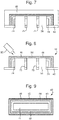
- FIGS 5 to 8 schematically depict stages of a method for manufacturing a membrane assembly 80 for EUV lithography according to an embodiment of the invention.
- a wet etchant such as KOH is used to selectively remove the inner region 71 and any bridge region 73 of the planar substrate 41.
- the etch mask layer 49 is chemically resistant to the wet etchant.
- Other wet etchants such as TMAH (tetramethylammonium hydroxide) and EDP (an aqueous solution of ethylene diamine and pyrocatechol) can be used.
- the stack 40 is provided with a mechanical protection material 66, shown in Figure 5 .
- the mechanical protection material 66 is configured to mechanically protect the border region 72 during the step of selectively removing the inner region 71 of the planar substrate 41.
- Figure 6 shows the stack 40 after the step of selectively removing the inner region 71 and the bridge region 73 of the planar substrate 41.
- the oxidized layer 42 protects the membrane from the wet etching step.
- the step of selectively removing the inner region 71 and any bridge region 73 of the planar substrate 41 can result in damage to the membrane assembly 80 during its manufacture.
- the stack 40 is particularly thin.
- the stack 40 comprises a mixture of extremely thin portions (where the inner region 71 has been removed) and thick portions (corresponding to the border 75 where the border region 72 of the planar substrate 41 has not been removed). This can result in mechanical stresses on the stack 40. It is possible for the stack 40 to break, or undesirably be damaged in other ways.
- the mechanical protection material 66 is thick enough to provide sufficient mechanical protection to the stack 40. In an embodiment the mechanical protection material has a thickness of at least about 1 ⁇ m, and optionally at least about 2 ⁇ m. In an embodiment the mechanical protection material 66 is thin enough so as to sufficiently reduce the process time required for applying the mechanical protection material 66. In an embodiment the mechanical protection material has a thickness of at most about 10 ⁇ m, and optionally at most about 5 ⁇ m. In an embodiment the mechanical protection material has a thickness of about 4 ⁇ m.
- the mechanical protection material 66 is sufficiently mechanically robust so as to provide mechanical protection to the border region 72 during the step of selectively removing the inner region 71 of the planar substrate 41.
- the mechanical protection material 66 may be a conformal coating for protecting the coated surface, having good barrier properties such as being resistant to solvents (e.g. insoluble at room temperature), moisture, corrosion, chemical attack. It is generally desired that the mechanical protection material 66 provides a uniform layer thickness with no pinholes.
- the step of selectively removing the inner region 71 of the planar substrate 41 comprises using a chemical etchant so as to selectively remove the inner region 71 of the planar substrate 41.
- the chemical etchant is KOH providing a temporary wet-etch protection.
- the mechanical protection material is chemically resistant to the chemical etchant.
- the mechanical protection material 66 is chemically resistant to KOH. This means that when the chemical etchant is used, the mechanical protection material 66 is either not etched away at all, or is etched away at a much lower etching rate compared to the inner region 71 of the planar substrate 41.
- the mechanical protection material 66 is applied as a continuous layer having substantially no holes in it.
- the mechanical protection material 66 forms a layer that is impermeable. During a process step of selectively removing parts of the planar substrate 41 using an etchant, the etchant cannot diffuse through the mechanical protection material 66 applied to the stack 40.
- the planar substrate 41 comprises an oxidized layer 42.
- the oxidized layer 42 is part of the planar substrate 41.
- the rest of the planar substrate 41 forms a non-oxidized layer of the planar substrate 41.
- the oxidized layer 42 is a sacrificial layer.
- the oxidized layer 42 forms an etch barrier when the non-oxidized layer of the planar substrate 41 is etched.
- the planar substrate 41 is etched from the bottom side.
- the oxidized layer 42 is resistant to the wet etchant.
- the oxidized layer 42 has a thickness greater than 100 nm, optionally greater than 200 nm, and optionally greater than 300 nm.
- the oxidized layer 42 has a thickness of about 350 nm or about 400 nm.
- the oxidized layer 42 is formed as a thin layer of oxide on outer surfaces of the planar substrate 41.
- the oxidized layer 42 is formed by a thermal oxidation process, for example as a thermal wet oxide.
- the oxidized layer 42 and the etchant used for etching the planar substrate 41 are configured such that the etch rate of the oxidized layer 42 in the etchant is less than about 5 nm/minute, for example about 3 nm/minute.
- the oxidized layer 42 comprises amorphous silicon dioxide.
- the stack 40 comprises a lower sacrificial layer 43.
- the lower sacrificial layer 43 protects the at least one membrane layer 45, 50 during the selective removal of any layer such as the oxidized layer 42 of the planar substrate 41 present at the bottom of the membrane.
- the thickness of the lower sacrificial layer 43 is not particularly limited. In an embodiment the thickness of the lower sacrificial layer 43 is at least about 5 nm, and optionally at least about 10 nm. In an embodiment the thickness of the lower sacrificial layer 43 is at most about 100 nm, and optionally at most about 50 nm. In an embodiment the thickness of the lower sacrificial layer 43 is about 20 nm.
- the lower sacrificial layer 43 is formed from a material such as amorphous silicon. However, this is not necessarily the case.
- the method of depositing the lower sacrificial layer 43 onto the stack 40 is not particularly limited.
- the lower sacrificial layer 43 is applied to the stack 40 by chemical vapour deposition.
- the lower sacrificial layer 43 is applied to the stack 40 by low pressure chemical vapour deposition at a temperature in a range from 300 to 700°C.
- this is not necessarily the case.
- the lower sacrificial layer 43 is applied to the stack 40 by a sputtering method or by a thin filming method, for example.
- Figure 7 schematically depicts the stack 40 after the step of etching the oxidized layer 42 and the lower sacrificial layer 43.
- the method for manufacturing the membrane assembly 80 comprises removing the mechanical protection material 66.
- the mechanical protection material 66 is removed using a fluoride etchant.
- a fluoride etchant instead of an oxidizing etchant, there is a reduced possibility of the membrane of the membrane assembly 80 being oxidized during the step of removing the mechanical protection material 66.
- an oxidizing etchant can be used to remove the mechanical protection material 66. This can result in unwanted, non-uniform and uncontrolled oxidation of the upper capping film 46 of the membrane assembly 80. For example, if an oxidative plasma is used to remove the mechanical protection material 66, then the membrane of the membrane assembly 80 can be less uniform. Oxidation of the upper capping film 46 can add oxygen atoms to the membrane such that the membrane becomes thicker in some places. This can increase the absorption of EUV radiation.
- the membrane of the membrane assembly 80 is expected to be more uniform and have a more controlled shape. This is expected to improve the imaging properties of the membrane assembly 80, for example reducing the level of absorption of EUV radiation.
- the fluoride etchant comprises a xenon difluoride (XeF 2 ) plasma.
- XeF 2 xenon difluoride
- Other fluoride etchants can be used as appropriate.
- the stack 40 comprises an upper sacrificial layer 47.
- the upper sacrificial layer 47 is disposed such that the membrane layer 45, 50 is disposed between the planar substrate 41 and the upper sacrificial layer 47.
- the other features relating to the upper sacrificial layer 47 can be selected and varied in the same way that the features of the lower sacrificial layer 43 can be selected and varied.
- the features of the lower sacrificial layer 43 were described above with particular reference to Figure 5 . Accordingly, the further features of the upper sacrificial layer 47 will not be discussed in any further detail here.
- the method for manufacturing the membrane assembly 80 comprises selectively removing the inner region 71 and any bridge region 73 of the planar substrate 41.
- the membrane assembly 80 comprises a membrane from the membrane layer 50 and a border 75 holding the membrane.
- the border 75 is formed from the border region 72 of the planar substrate 41.
- the border 75 improves the mechanical stability of the membrane of the membrane assembly 80.
- An embodiment of the invention is expected to achieve an improvement in the mechanical stability of the membrane assembly 80. This makes it easier to package and transport the membrane assembly 80 without the membrane assembly 80 being damaged. This also makes it easier for the membrane assembly 80 to be attached to the patterning device MA by a frame without the membrane assembly 80 being damaged.
- the border 75 of the membrane assembly 80 is configured to be connected to the frame that connects the membrane assembly 80 to the patterning device MA.
- the frame does not need to be attached directly to the membrane of the membrane assembly 80.
- the frame can be attached to the border 75 of the membrane assembly 80. This reduces the possibility of the membrane of the membrane assembly 80 being damaged during the process of fitting the membrane assembly 80 to the patterning device MA.
- the etch mask layer 49 is deposited by chemical vapour deposition.
- the etch mask layer 49 is applied by low pressure chemical vapour deposition at a temperature of about 850°C.
- the nature of the membrane layer 45 can be changed.
- the membrane layer 45 when the membrane layer 45 is initially applied as amorphous silicon, the membrane layer 45 may be transformed into a membrane layer 50 formed of poly crystalline or nanocrystalline silicon.
- the temperature causes the amorphous silicon to crystallise into polycrystalline or nanocrystalline silicon.
- Polycrystalline silicon and nanocrystalline silicon each have high transmission for EUV radiation.
- Polycrystalline silicon and nanocrystalline silicon each have good mechanical strength. It is easier to manufacture the membrane assembly 80 having a membrane formed from polycrystalline or nanocrystalline silicon than to fabricate a membrane formed of another material such as a multi-lattice material.
- Polycrystalline silicon and nanocrystalline silicon substantially filter EUV radiation.
- the membrane of the membrane assembly 80 is not essential for the membrane of the membrane assembly 80 to be formed from polycrystalline or nanocrystalline silicon.
- the membrane of the membrane assembly 80 is formed from a multi-lattice membrane or a silicon nitride.
- the membrane of the membrane assembly 80 is formed from monocrystalline silicon.
- the monocrystalline silicon membrane can be formed by a silicon on insulator (SOI) technique.
- SOI substrate is a substrate comprising a silicon carrier substrate with a thin, monocrystalline silicon layer on top of a buried isolating SiO 2 layer.
- the thickness of the monocrystalline silicon layer can range between about 5 nm to about 5 ⁇ m.
- the silicon membrane layer is present on the SOI substrate before the SOI substrate is used in the method of manufacture.
- Figures 9 to 12 schematically depict stages in a method for manufacturing a membrane assembly 80 for EUV lithography, according to an embodiment of the invention.
- Figure 9 depicts the stack 40, which comprises the planar substrate 41, the oxidized layer 42, the lower sacrificial layer 43, the lower capping film 44, the at least one membrane layer 45 and the upper capping film 46.
- the oxidized layer 42, the lower sacrificial layer 43, the lower capping film 44 and the upper capping film 46 are optional.
- the method comprises the step of forming a bridge groove 81.
- the bridge groove 81 is a groove that is termed a "bridge" groove because it is formed at a position corresponding to the bridge region 73 of the planar substrate 41.
- the bridge groove 81 is formed through the at least one membrane layer 45 adjacent to the bridge region 73 of the planar substrate 41.
- the bridge groove 81 is formed through the lower capping film 44 and the upper capping film 46.
- the bridge groove 81 is formed through the layers that form the membrane in the membrane assembly 80.
- the bridge groove 81 is a deep through-hole in the pellicle bulk.
- the purpose of the bridge groove 81 is so that it is not necessary to break the at least one membrane layer 45 above the bridge region 73 at the end of the method for manufacturing the membrane assembly 80.
- the bridge groove 81 is formed by a laser, (N)IR radiation or EUV radiation.
- a laser, (N)IR radiation or EUV radiation is used to burn through the at least one membrane layer 45 and the lower capping film 44 and the upper capping film 46.
- the method comprises forming a rectangular groove (i.e. the bridge groove 81) in a non-rectangular stack 40. By forming a rectangular groove in a non-rectangular stack 40, the membrane is separated from the part of the at least one membrane layer 45, 50 that is to be discarded at a relatively early stage in the method. Accordingly, it is not necessary to mechanically break the at least one membrane layer 50 at the end of the manufacturing method in order to provide a membrane having the desired shape.
- the bridge groove 81 is formed in a rectangular shape (when the stack 40 is viewed in plan view).
- the bridge groove 81 can be filled with a filler material such as a sacrificial layer or a mechanical protection material.
- a filler material such as a sacrificial layer or a mechanical protection material.
- an upper sacrificial layer 47 is provided to the stack 40.
- the material of the upper sacrificial layer 47 fills in the bridge groove 81.
- a material such as the mechanical protection material 66 can be used to fill the bridge groove 81.
- Figure 12 schematically depicts a later step in the method for manufacturing the membrane assembly 80.
- the inner region 71 and the bridge region 73 of the planar substrate 41 have been selectively removed (together with any oxidized layer 42 and any lower sacrificial layer 43).
- the upper sacrificial layer 47 has also been removed.
- the edge section (formed by the edge region 74 of the planar substrate 41) is separated from the border 75.
- the edge section is separated from the border 75 by selectively removing the bridge region 73 of the planar substrate 41.
- the bridge groove 81 becomes an open area allowing removal of the edge section without cutting or breaking the at least one membrane layer 50.
- the membrane of the membrane assembly 80 is separated away (via the bridge groove 81 which forms a through-groove in the stack 40) from the peripheral portion of the at least one membrane layer 50 that is to be discarded.
- Contaminant particles can include flakes of silicon. Any such contaminant particles on the finalized membrane assembly 80 can reduce the optical performance of the membrane assembly 80. Loose hanging flakes of silicon that overlap with the border 75 can be released and adhered to the membrane of the membrane assembly 80. The contaminant particles can adhere relatively easily to the membrane because the contaminant particles are so thin.
- the bridge groove 81 is formed such that part of the at least one membrane layer 45 extends radially outwardly of the border region 72 of the planar substrate 41. This is shown in Figure 10 , where part of the at least one membrane layer 45 extends outwardly beyond the border region 72. Accordingly, when the edge section is separated from the border 75 (at the end of the method for manufacturing the method for manufacturing the membrane assembly 80), that part of the membrane layer 50 extends radially outwardly of the border 75. This is shown in Figure 12 .
- a pillar can be provided in the bridge groove 81.
- the pillar is for holding the gap between the membrane and the peripheral part of the at least one membrane layer 45 that is to be discarded.
- the stack 40 is rectangular.
- the planar substrate 41 can have substantially the same shape as the desired shape of the membrane assembly 80 produced by the method.
- edges of the at least one membrane layer 45 in the stack 40 are rounded or chamfered.
- the edges of the membrane assembly 80 are less sharp.
- anisotropic etching can result in particularly sharp edges for the membrane assembly 80.
- the edges of the membrane of the membrane assembly 80 can have the shape of a sharp triangle. This increases the possibility of the corner of the edge breaking away resulting in the creation of contaminant particles.
- the contaminant particles can have a diameter in the region of from about 20 nm to about 1 ⁇ m.
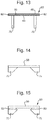
- Figure 13 depicts a membrane assembly 80 according to an embodiment of the invention.
- the method comprises applying a passivation coating 82 to the edges of the at least one membrane layer 50 after separating the edge section from the border 75.
- the edges can be coated with a thick sticky layer.
- a spray coating may be used.
- the thickness of the passivation coating 82 is in the range of from about 1 ⁇ m to about 10 ⁇ m.
- the passivation coating 82 passivates the edge of the at least one membrane layer 50.
- the passivation coating 82 is applied in the form of a sticky tape applied around the edge.
- the passivation coating 82 is applied to the edge of the earliest one membrane layer 50 after chipping the unwanted peripheral section of the at least one membrane layer 50 off.
- the passivation coating 82 is applied using atomic layer deposition, chemical vapour deposition, electroplating or dip coating.
- the passivation coating 82 comprises a metal such as Ru.
- the passivation coating 82 may also comprise a silicide, an oxide or a nitride.
- the passivation coating 82 can be deposited to the edge of the at least one membrane layer 50 by, for example, chemical vapour deposition.
- the passivation coating 82 is applied all around the membrane assembly 80 (not just to the edges of the at least one membrane layer 50).
- the passivation coating 82 can be applied all around the membrane assembly 80 via atomic layer deposition or chemical vapour deposition. Electroplating can also be used to make conformal Ru coatings.
- to Ru layers are provided for protection of the membrane assembly 80.
- the passivation coating 82 is applied using physical vapour deposition.
- a shadow mask may be used such that only the edges of the at least one membrane layer 50 receives the passivation coating layer 82.
- the passivation coating 82 can be coated locally onto the edges of the silicon membrane via physical vapour deposition.
- a shadow mask can be used to mask the inner part of the membrane.
- the rest of the membrane can be sputtered by the material of the passivation coating 82.
- this process which may be called shadow sputtering, may be appropriate if the mechanical protection material 66 (e.g. a densely crosslinked polymer) is removed using a non-oxidizing plasma.
- the passivation coating 82 reduces the possibility of the corner of the edge of the membrane breaking away to create contaminant particles. Accordingly, an embodiment of the invention is expected to achieve a reduction in contaminant particles adhered to the membrane of the membrane assembly 80. This can result in a membrane assembly 80 having improved transmission for EUV radiation and more consistent optical properties across its area.
- the at least one membrane layer 45 comprises an amorphous material.
- an amorphous material instead of crystalline silicon, for example, the edges of the membrane assembly 80 will be less brittle. Accordingly, using an amorphous material can reduce the possibility of contaminant particles being produced when the membrane assembly 80 is broken away from the unwanted sections of the planar substrate 41 and the at least one membrane layer 50.
- the method for manufacturing the membrane assembly 80 comprises oxidizing or nitriding the edges of the at least one membrane layer 50 after separating the edge section from the border 75.
- the membrane is made less reactive.
- the native oxide is less reactive than pure silicon. Accordingly, by oxidizing or nitriding the edges of the silicon membrane, the chances of particle debris being created that contact with pellicle tooling is reduced.
- Dip coating can be used to selectively apply Ru layers to protect the edges of the silicon membrane.
- Figure 14 schematically depicts a membrane assembly in which the at least one membrane layer 50 spans across the border 75 (which may also be called a frame).
- the at least one membrane layer 50 is deposited directly on top of the planar substrate 41.
- the membrane is then made free-standing due to selectively anisotropically back etching of the planar substrate 41.
- the material for the at least one membrane layer 50 is SiN. Other materials are also possible.
- Step defects can also result from the anisotropic etching step used in the fabrication process.
- the anisotropic etching follows crystallographic planes. Accordingly, step defects can exhibit particularly sharp corners where particularly high stress concentrations can occur. This can result in failure or breaking of the membrane assembly 80 at positions where the particularly high stress concentrations occur.
- the shape of the border 75 may vary depending on the etching process used to selectively remove parts of the planar substrate 41.
- the shape of the border 75 may also vary depending on the material used to form the border 75.
- the shape of the border 75 shown in Figure 14 is a typical shape that results from anisotropic etching when the material used to form the planar substrate 41 is a crystalline material.
- Figure 15 schematically depicts a membrane assembly 80 according to an embodiment of the invention.
- the stack 40 is provided with an intermediate layer 83.
- the intermediate layer 83 is positioned between the planar substrate 41 and the at least one membrane layer 45.
- the method for manufacturing the membrane assembly 80 comprises isotropically etching the intermediate layer 83 after the step of selectively removing the inner region 71 of the planar substrate 41.
- the intermediate layer 83 is purposely introduced between the border 75 and the at least one membrane layer 50.
- the intermediate layer is thicker than the at least one membrane layer 50.
- the intermediate layer 83 is etched isotropically.
- the intermediate layer 83 is etched using an etching agent that is selective.
- the intermediate layer 83 is etched, without the at least one membrane layer 50 being etched.
- the isotropically etched intermediate layer 83 smoothens the sharp edges of the transition from the border 75 to the at least one membrane layer 50. This results in significantly lower stress concentrations, and thus a reduced chance of failure of the membrane.
- Isotropic etching etches at the same rate in all directions. On the other hand, anisotropic etching etches significantly faster in certain directions due to crystal plane orientations. Anisotropic etching inherently leads to atomically sharp edges and thus higher stress concentrations. For glassy or amorphous materials, etching is typically isotropic.
- the intermediate layer 80 comprises silicon dioxide or amorphous silicon or a metal layer.
- the isotropically etched intermediate layer 83 mitigates stresses at the locations of any step defects.
- the intermediate layer 83 also reduces stresses throughout the entire transition from the border 75 to the membrane.
- the intermediate layer 83 also reduces stresses that the corners of the membrane assembly 80.
- the intermediate layer 83 is significantly thicker than the membrane.
- the intermediate layer 83 has a thickness of at least 50 nm, optionally at least 100 nm.
- the intermediate layer 83 has a thickness of at most 500 nm, optionally at most 200 nm.
- the etching agent used to isotropically etch the intermediate layer 83 is selective. This means that the etching agent is configured to etch the intermediate layer 83 and not the membrane structure.
- the method for manufacturing the membrane assembly 80 comprises changing a pre-tension in the at least one membrane layer 45 of the stack 40 by one or more of an annealing process, ion beam modification, controlling a pressure applied to the stack 40 and controlling a temperature applied to the stack 40.
- Pre-tension is applied to the at least one membrane layer 45 during the manufacturing process so that the membrane of the membrane assembly 80 will be straight and flat during use. If no pre-tension is applied, then the membrane may be undesirably flappy or wrinkled (wrinkling leading also to a non-uniform membrane thickness). A loose or a non-uniform thickness membrane can have poorer imaging properties. However, if the pre-tension is too high, then the membrane can be brittle and more susceptible to breaking. Accordingly, it is desirable to control the pre-tension to be within a target range.
- the pre-tension of the at least one membrane layer 45 is controlled to be at least 80 MPa tensile. This pre-tension is built in when the at least one membrane layer 50 is formed. The pre-tension can henceforth be altered by heat treatment. In an embodiment the pre-tension can be applied to the lower capping film 44 and/or to the upper capping film 46. In an embodiment the pre-tension is applied to both the at least one membrane layer 45 (that forms the membrane) as well as to the lower capping film 44 and the upper capping film 46.
- an annealing step is performed to increase the crystalline fraction of the at least one membrane layer 45 and/or to increase the stress in the at least one membrane layer 45.
- Ion beam modification i.e. implantation
- Pre-tension can be introduced into the at least one membrane layer 45 between any other steps of the method for manufacturing the membrane assembly 80.
- Pre-tension (which may also be called pre-stress) is introduced into the membrane in order to prevent heat induced buckling at higher temperatures during use of the membrane assembly 80.
- the method for manufacturing the membrane assembly 80 comprises introducing pre-tension into the membrane so that the membrane will have a stress closer to its design value in use.
- the membrane In use (e.g. when the membrane assembly 80 is used as a pellicle for a patterning device MA), the membrane is subjected to EUV radiation.
- the EUV radiation applied to the membrane assembly 80 during use can increase the tension in the membrane.
- the method comprises introducing pre-tension into the membrane to a bevel below the desired tension during use of the membrane assembly 80.
- the stack 40 may need to be protected with a mechanical protection material 66, which can be removed later after the wet etching step.
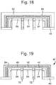
- Figures 16 to 19 depict schematically steps of a method for manufacturing the membrane assembly 80 according to an embodiment which is not part of the invention.
- Figure 16 schematically depicts the stack 40.
- the stack 40 is provided with an etch stop layer 84.
- the etch stop layer 84 is for protecting the stack 40 during the step of removing the mechanical protection material 66 (which is shown in Figure 17 ).
- the etch stop layer 84 is applied to the top of the stack 40 before the mechanical protection material 66 is applied to the stack 40.
- the planar substrate 41 can be etched away for example using a wet etching.
- the mechanical protection material 66 protects in this case the rest of the stack 40 from the liquid etchant. Further etching processes may be required to etch away the oxidized layer 42 and any lower sacrificial layer 43.
- the etch stop layer 84 may be applied to the bottom of the stack 40.
- the etch stop layer 84 applied to the bottom of the stack 40 is for protecting the membrane from the etchant used to remove the mechanical protection material 66.
- the etch stop layer 84 remains in place.
- an oxidizing plasma is used as the etchant to remove the mechanical protection material 66.
- the etch stop layer 84 is resistant to oxidizing plasma.
- the etch stop layer 84 has a thickness in the region of from about 10 nm to about 100 nm.
- the material used for the etch stop layer 84 is an oxide, which cannot be further oxidized by the oxidizing plasma used to remove the mechanical protection material 66.
- the etch stop layer 84 comprises an oxide of silicon.
- the etch stop layer 84 can then be removed after the step of removing the mechanical protection material 66. Accordingly, by providing the etch stop layer 84, a wet etchant can be used in conjunction with the mechanical protection material 66, while reducing the possibility of the membrane becoming oxidized when the mechanical protection material 66 is removed. Accordingly, an embodiment of the invention is expected to achieve an increase in the uniformity of the membrane of the membrane assembly 80.
- Figures 20 to 27 schematically depict steps of a method for manufacturing the membrane assembly 80 according to an embodiment which is not part of the invention.
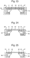
- the method depicted in Figures 20 to 27 does not require any mechanical protection material 66 to be used. Accordingly, the method avoids any step of removing the mechanical protection material 66, which could otherwise damage the membrane.
- the stack 40 comprises the planar substrate 41 and the oxidation layer 42.
- the oxidation layer 42 is for stopping the wet etching process that is used to selectively use parts of the planar substrate 41.
- the stack 40 comprises a lower thick etch barrier 86 and a lower thin etch barrier 87.
- the lower thick etch barrier 86 and the lower thin etch barrier 87 are deposited between the at least one membrane layer 45 and the oxidation layer 42 of the planar substrate 41.
- the lower thick etch barrier 86 is deposited between the lower thin etch barrier 87 and the oxidation layer 42.
- An upper thin etch barrier 88 and an upper thick etch barrier 89 are provided to the stack 40 outside of the at least one membrane layer 45.
- the material used for the upper thick etch barrier 89 is the same as the material used for the lower thick etch barrier 86.
- the material used for the upper thin etch barrier 88 is the same as the material used for the lower thin etch barrier 87.
- the stack 40 is provided with a wet-etching barrier 90.
- the wet-etching barrier is for protecting the stack 40 from the wet etchant used to selectively remove parts of the planar substrate 41.
- the method comprises a step of selectively removing parts of the wet-etching barrier 90, the upper thick etch barrier 89, the upper thin etch barrier 88, the at least one membrane layer 45, the lower thin etch barrier 87, the lower thick etch barrier 86 and the oxidation layer 42.
- this etching process is performed by a dry etching technique. A mask may be used to remove the layers selectively. By performing the dry etching process, the desired portion of the planar substrate 41 is exposed at the bottom of the stack 40.
- the method comprises selectively removing the inner region of the planar substrate 41.
- the selective removal of parts of the planar substrate 41 may be performed using a wet etching process.
- a wet etchant such as KOH may be used.
- the oxidation layer 42 between the membrane and the planar substrate 41 stops the wet etching process from reaching the membrane.
- the method comprises selectively removing the oxidation layer 42 that acted as a barrier for the wet etchant.
- the oxidation layer 42 may be removed by a dry etching technique, for example.
- the method comprises selectively removing the lower thick etch barrier 86.
- the lower thick etch barrier 86 may be set to be removed by a dry etching technique.
- the lower thick etch barrier 86 and the upper thick etch barrier 89 comprise a silicon nitride.
- the lower thin etch barrier and the upper thin etch barrier comprise a silicon nitride.
- the upper thick etch barrier 89 may be removed at the same time as the lower thick etch barrier 86 is removed.
- the method comprises removing the lower thin etch barrier 87 and the upper thin etch barrier 88.
- the lower thin etch barrier 87 and the upper thin etch barrier 88 may be removed substantially simultaneously.
- a dry etching technique may be used.
- the method comprises separating the membrane from the peripheral sections of the at least one membrane layer 45 that are to be discarded (rather than form part of the membrane).
- the separation is performed by a laser dicing process. Accordingly, the membrane is extended across the remaining parts of the stack 40, which form the order of the membrane assembly 80.
- the method comprises providing a capping layer 93 to the membrane assembly 80.
- the capping layer 93 is provided all around the membrane assembly 80.
- the capping layer 93 is made of the same material as the lower capping film 44 or the upper capping film 46 described in relation to other embodiments.
- the stack 40 when the stack 40 undergoes the wet etching process, the at least one membrane layer 45 is supported on the upper and lower sides by the lower thick edge barrier 86 and the upper thick etch barrier 89. Accordingly, the lower thick etch barrier 86 and the upper thick etch barrier 89 provide mechanical support to the at least one membrane layer 45.
- This allows the stack 40 to be handled by tools with a reduced possibility of the membrane breaking during the manufacturing process. For example, the stack 40 can be placed into a bath of wet etchant and removed from the bath of wet etchant with a reduced possibility of the membrane failing or breaking.
- an embodiment of the invention is expected to make it easier to manufacture a membrane assembly 80, with a reduced possibility of the membrane breaking during manufacture and a reduced possibility of the membrane becoming oxidized during manufacture.
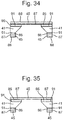
- Figures 28 to 35 depict steps of an alternative embodiment which is not part of the invention, which also avoids the necessity for any mechanical protection material 66 being applied and removed from the stack 40.
- the stack comprises the planar substrate 41, a silicon nitride layer 91, the lower thick etch barrier 86, the lower thin etch barrier 87, the at least one membrane layer 45, the upper thin etch barrier 88 and the upper thick etch barrier 89.
- the stack 40 does not require the outer wet etching barrier 90.
- the method comprises cutting the stack 40 so as to provide a stack 40 having the desired shape of the membrane assembly 80.
- the stack 40 is laser diced into a rectangular shape. This means that it is not necessary to perform any dicing step or breaking step later on in the method which could otherwise result in the creation of contaminant particles that stick to the membrane. Contaminant particles that are produced from any dicing step early on in the method can be more easily cleaned away without the contaminant particles adhering to the membrane.
- the method comprises applying an outer sacrificial layer 92 to the stack 40.
- the outer sacrificial layer 92 comprises a silicon nitride.
- the outer sacrificial layer 92 is for protecting the stack 40 from the wet etchant used to selectively remove parts of the planar substrate 41.
- the method comprises the steps of selectively etching the outer sacrificial layer 92, the upper thick etch barrier 89, the upper thin etch barrier 88, the at least one membrane layer 45, the lower thin etch barrier 87, the lower thick etch barrier 86 and the silicon nitride layer 91.
- the wet etchant may be KOH.
- the stack 40 is placed into a bath of KOH and subsequently removed from the bath of KOH using a handling tool. The presence of the lower thick etch barrier 86 and the upper thick etch barrier 89 mechanically supports the at least one membrane layer 45 so that the membrane is less likely to be damaged during the process of etching the planar substrate 41.
- the method comprises etching the outer sacrificial layer 92 and the silicon nitride layer 91.
- an oxidation layer 42 of the planar substrate 41 may be provided.
- the outer sacrificial layer 92 and the silicon nitride layer 91 may be removed substantially simultaneously using a dry etching process.
- the method comprises selectively removing the upper thick etch barrier 89 and the lower thick etch barrier 86. These may be removed using a dry etching process. As depicted in Figure 35 , in an embodiment the method comprises removing the lower thin etch barrier 87 and the upper thin etch barrier 88. This exposes the membrane at that top and bottom of the stack 40. In an embodiment the method further comprises applying the capping layer 93 to the outside of the membrane assembly 80 so as to provide a protective layer to the membrane, as depicted in Figure 27 .
- a suction (flow) is applied during the edge breaking step.
- suction is applied locally.
- the suction is applied in order to remove any contaminant particles that are created during the separation step.
- a suction device 85 applies a suction pressure to the region where the separation is formed.
- the suction device 85 reduces the possibility of contaminant particles adhering to the membrane of the membrane assembly 80.
- the suction device 85 is simultaneously applied to all of the regions where the separation is taking place.
- the suction device 85 may take the form of a rectangular shape that corresponds to the shape of the membrane assembly 80.
- the suction device 85 is moved during the separating step so as to be adjacent to wherever the at least one membrane layer 50 is being broken.
- the membrane assembly 80 can be used as a pellicle placed in front of the patterning device MA and thus protect the patterning device MA.
- An embodiment of the invention is expected to achieve a reduction of fragility of a pellicle.
- An embodiment of the invention is expected to make it easier to produce membrane assemblies in high volume.
- An embodiment of the invention is expected to enable the processing of a free standing membrane integrated in a frame.
- the membrane assembly 80 is configured to transmit at least 90% of radiation having a wavelength of 13.5 nm. In an embodiment the membrane assembly 80 is configured to transmit less than 5% of DUV radiation (approximately 100-400 nm).
- the membrane layer 50 of the membrane assembly 80 comprises silicon. Silicon is one of the most transparent elements to EUV radiation. Silicon is a commonly processed and available material. In an embodiment the membrane layer 50 is capped with Ru, Zr, Mo, a silicon oxide, a zirconium oxide, an aluminum oxide, boron nitride, a ruthenium oxide, a ruthenium nitride, a zirconium nitride, a molybdenum oxide or a molybdenum nitride. Such a combination is expected to reduce hydrogen-induced outgassing and the consequent redeposition of silicon.
- the membrane assembly 80 may be used in an environment that contains hydrogen radicals.
- Tungsten is for example a material which can withstand hydrogen plasma and it is also reasonably stable against oxidation up to 400 °C. Tungsten has also a high melting point (3422 °C) and it has a low coefficient of thermal expansion compared to other metals.
- the membrane assembly 80 is applied as a pellicle or as part of a dynamic gas lock.
- the membrane assembly 80 can be applied in other filtration areas such as identification, or for beam splitters.
- the substrate referred to herein may be processed, before or after exposure, in for example a track (a tool that typically applies a layer of resist to a substrate and develops the exposed resist), a metrology tool and/or an inspection tool. Where applicable, the disclosure herein may be applied to such and other substrate processing tools. Further, the substrate may be processed more than once, for example in order to create a multi-layer IC, so that the term substrate used herein may also refer to a substrate that already contains multiple processed layers.
- the various lacquer layers may be replaced by non-lacquer layers that perform the same function.
Landscapes
- Physics & Mathematics (AREA)
- General Physics & Mathematics (AREA)
- Engineering & Computer Science (AREA)
- Plasma & Fusion (AREA)
- Health & Medical Sciences (AREA)
- Environmental & Geological Engineering (AREA)
- Epidemiology (AREA)
- Public Health (AREA)
- Exposure And Positioning Against Photoresist Photosensitive Materials (AREA)
- Exposure Of Semiconductors, Excluding Electron Or Ion Beam Exposure (AREA)
- Preparing Plates And Mask In Photomechanical Process (AREA)
Description
- The present invention relates to a method for manufacturing a membrane assembly, and to a membrane assembly.
- A lithographic apparatus is a machine that applies a desired pattern onto a substrate, usually onto a target portion of the substrate. A lithographic apparatus can be used, for example, in the manufacture of integrated circuits (ICs). In that instance, a patterning device, which is alternatively referred to as a mask or a reticle, may be used to generate a circuit pattern to be formed on an individual layer of the IC. This pattern can be transferred onto a target portion (e.g., comprising part of, one, or several dies) on a substrate (e.g., a silicon wafer). Transfer of the pattern is typically via imaging onto a layer of radiation-sensitive material (resist) provided on the substrate. In general, a single substrate will contain a network of adjacent target portions that are successively patterned.
- Lithography is widely recognized as one of the key steps in the manufacture of ICs and other devices and/or structures. However, as the dimensions of features made using lithography become smaller, lithography is becoming a more critical factor for enabling miniature IC or other devices and/or structures to be manufactured.
- A theoretical estimate of the limits of pattern printing can be given by the Rayleigh criterion for resolution as shown in equation (1):

- In order to shorten the exposure wavelength and, thus, reduce the minimum printable size, it has been proposed to use an extreme ultraviolet (EUV) radiation source. EUV radiation is electromagnetic radiation having a wavelength within the range of 10-20 nm, for example within the range of 13-14 nm. It has further been proposed that EUV radiation with a wavelength of less than 10 nm could be used, for example within the range of 5-10 nm such as 6.7 nm or 6.8 nm. Such radiation is termed extreme ultraviolet radiation or soft x-ray radiation. Possible sources include, for example, laser-produced plasma sources, discharge plasma sources, or sources based on synchrotron radiation provided by an electron storage ring.
- A lithographic apparatus includes a patterning device (e.g., a mask or a reticle). Radiation is provided through or reflected off the patterning device to form an image on a substrate. A membrane assembly may be provided to protect the patterning device from airborne particles and other forms of contamination. The membrane assembly for protecting the patterning device may be called a pellicle. Contamination on the surface of the patterning device can cause manufacturing defects on the substrate. The membrane assembly may comprise a border and a membrane stretched across the border. It is difficult to manufacture the membrane assembly without the membrane assembly being deformed in the process, for example because of the thickness of the membrane.
- It is also difficult to manufacture the membrane assembly without the membrane assembly being damaged or contaminated in the process. For example, the membrane may be undesirably oxidized or have unwanted contaminant particles deposited on the membrane during the process of manufacturing the membrane assembly.
- It is desirable to reduce the possibility of a membrane assembly such as a pellicle being deformed, damaged or contaminated during its manufacture.
-
US 6623893 B1 describes a pellicle comprising a silicon film under tensile stress, an anti-reflective coating and a substrate coupled to the periphery of the film. -
EP 2423747 A1 describes a pellicle comprising a film of single crystal silicon supported by a porous portion and an outer frame portion. - According to an aspect of the invention, there is provided a method for manufacturing a membrane assembly for EUV lithography, the method comprising: providing a stack comprising a planar substrate and at least one membrane layer, wherein the planar substrate comprises an inner region, a border region around the inner region, a bridge region around the border region and an edge region around the bridge region; forming a bridge groove through the at least one membrane layer adjacent the bridge region of the planar substrate; selectively removing the inner region and the bridge region of the planar substrate, such that the membrane assembly comprises: a membrane formed from the at least one membrane layer; a border holding the membrane, the border formed from the border region of the planar substrate; an edge section around the border, the edge section formed from the edge region of the planar substrate; and a bridge between the border and the edge section, the bridge formed by the at least one membrane layer; and separating the edge section from the border such that the at least one membrane layer adjacent the edge section is separated from the membrane by the bridge groove.
- According to an aspect of the invention, there is provided a membrane assembly for EUV lithography, the membrane assembly comprising a membrane formed from at least one membrane layer comprising silicon and a border holding the membrane, wherein the edges of the at least one membrane layer are oxidized or nitrided
- Embodiments which are not all part of the invention will now be described, by way of example only, with reference to the accompanying schematic drawings in which corresponding reference symbols indicate corresponding parts, and in which:
-
Figure 1 depicts a lithographic apparatus; -
Figure 2 is a more detailed view of the lithographic apparatus; -
Figures 3 and 4 schematically depict stages of a method for manufacturing a pellicle according to an embodiment of the invention; -
Figures 5 to 8 schematically depict stages of a method for manufacturing a pellicle according to an embodiment of the invention; -
Figures 9 to 12 schematically depict stages of a method for manufacturing a pellicle according to an embodiment of the invention; -
Figure 13 schematically depicts a membrane assembly according to an embodimen which is not part of the invention; -
Figure 14 schematically depicts a membrane assembly according to a comparative example; -
Figure 15 schematically depicts a membrane assembly according to an embodimen which is not part of the invention; -
Figures 16 to 19 schematically depict stages of a method for manufacturing a pellicle according to an embodiment which is not part of the invention; -
Figures 20 to 27 schematically depict stages of a method for manufacturing a pellicle according to an embodiment which is not part of the invention; and -
Figures 28 to 35 schematically depict stages of a method for manufacturing a pellicle according to an embodiment which is not part of the invention. - The features and advantages of the present invention will become more apparent from the detailed description set forth below when taken in conjunction with the drawings, in which like reference characters identify corresponding elements throughout. In the drawings, like reference numbers generally indicate identical, functionally similar, and/or structurally similar elements.
-
Figure 1 schematically depicts alithographic apparatus 100 including a source collector module SO. Theapparatus 100 comprises - an illumination system (or illuminator) IL configured to condition a radiation beam B (e.g., EUV radiation).
- a support structure (e.g., a mask table) MT constructed to support a patterning device (e.g., a mask or a reticle) MA and connected to a first positioner PM configured to accurately position the patterning device;
- a substrate table (e.g., a wafer table) WT constructed to hold a substrate (e.g., a resist-coated wafer) W and connected to a second positioner PW configured to accurately position the substrate; and
- a projection system (e.g., a reflective projection system) PS configured to project a pattern imparted to the radiation beam B by patterning device MA onto a target portion C (e.g., comprising one or more dies) of the substrate W.
- The illumination system IL may include various types of optical components, such as refractive, reflective, magnetic, electromagnetic, electrostatic or other types of optical components, or any combination thereof, for directing, shaping, or controlling radiation.
- The support structure MT holds the patterning device MA in a manner that depends on the orientation of the patterning device, the design of the lithographic apparatus, and other conditions, such as for example whether or not the patterning device is held in a vacuum environment. The support structure MT can use mechanical, vacuum, electrostatic or other clamping techniques to hold the patterning device MA. The support structure MT may be a frame or a table, for example, which may be fixed or movable as required. The support structure MT may ensure that the patterning device MA is at a desired position, for example with respect to the projection system PS.
- The term "patterning device" should be broadly interpreted as referring to any device that can be used to impart a radiation beam B with a pattern in its cross-section such as to create a pattern in a target portion C of the substrate W. The pattern imparted to the radiation beam B may correspond to a particular functional layer in a device being created in the target portion C, such as an integrated circuit.
- The patterning device MA may be transmissive or reflective. Examples of patterning devices include masks, programmable mirror arrays, and programmable liquid-crystal display (LCD) panels. Masks are well known in lithography, and include mask types such as binary, alternating phase-shift, and attenuated phase-shift, as well as various hybrid mask types. An example of a programmable mirror array employs a matrix arrangement of small mirrors, each of which can be individually tilted so as to reflect an incoming radiation beam in different directions. The tilted mirrors impart a pattern in a radiation beam, which is reflected by the mirror matrix.
- The projection system PS, like the illumination system IL, may include various types of optical components, such as refractive, reflective, magnetic, electromagnetic, electrostatic or other types of optical components, or any combination thereof, as appropriate for the exposure radiation being used, or for other factors such as the use of a vacuum. It may be desired to use a vacuum for EUV radiation since other gases may absorb too much radiation. A vacuum environment may therefore be provided to the whole beam path with the aid of a vacuum wall and vacuum pumps.
- As here depicted, the
lithographic apparatus 100 is of a reflective type (e.g., employing a reflective mask). - The
lithographic apparatus 100 may be of a type having two (dual stage) or more substrate tables WT (and/or two or more support structures MT). In such a "multiple stage" lithographic apparatus the additional substrate tables WT (and/or the additional support structures MT) may be used in parallel, or preparatory steps may be carried out on one or more substrate tables WT (and/or one or more support structures MT) while one or more other substrate tables WT (and/or one or more other support structures MT) are being used for exposure. - Referring to
Figure 1 , the illumination system IL receives an extreme ultraviolet radiation beam from the source collector module SO. Methods to produce EUV light include, but are not necessarily limited to, converting a material into a plasma state that has at least one element, e.g., xenon, lithium or tin, with one or more emission lines in the EUV range. In one such method, often termed laser produced plasma ("LPP") the required plasma can be produced by irradiating a fuel, such as a droplet, stream or cluster of material having the required line-emitting element, with a laser beam. The source collector module SO may be part of an EUV radiation system including a laser, not shown inFigure 1 , for providing the laser beam exciting the fuel. The resulting plasma emits output radiation, e.g., EUV radiation, which is collected using a radiation collector, disposed in the source collector module. The laser and the source collector module SO may be separate entities, for example when a CO2 laser is used to provide the laser beam for fuel excitation. - In such cases, the laser is not considered to form part of the
lithographic apparatus 100 and the radiation beam B is passed from the laser to the source collector module SO with the aid of a beam delivery system comprising, for example, suitable directing mirrors and/or a beam expander. In other cases the source may be an integral part of the source collector module SO, for example when the source is a discharge produced plasma EUV generator, often termed as a DPP source. - The illumination system IL may comprise an adjuster for adjusting the angular intensity distribution of the radiation beam. Generally, at least the outer and/or inner radial extent (commonly referred to as □ -outer and □ -inner, respectively) of the intensity distribution in a pupil plane of the illumination system IL can be adjusted. In addition, the illumination system IL may comprise various other components, such as facetted field and pupil mirror devices. The illumination system IL may be used to condition the radiation beam B, to have a desired uniformity and intensity distribution in its cross-section.
- The radiation beam B is incident on the patterning device (e.g., mask) MA, which is held on the support structure (e.g., mask table) MT, and is patterned by the patterning device MA. After being reflected from the patterning device (e.g., mask) MA, the radiation beam B passes through the projection system PS, which focuses the radiation beam B onto a target portion C of the substrate W. With the aid of the second positioner PW and position sensor PS2 (e.g., an interferometric device, linear encoder or capacitive sensor), the substrate table WT can be moved accurately, e.g., so as to position different target portions C in the path of the radiation beam B. Similarly, the first positioner PM and another position sensor PS1 can be used to accurately position the patterning device (e.g., mask) MA with respect to the path of the radiation beam B. The patterning device (e.g., mask) MA and the substrate W may be aligned using mask alignment marks M1, M2 and substrate alignment marks PI, P2.
- A
controller 500 controls the overall operations of thelithographic apparatus 100 and in particular performs an operation process described further below.Controller 500 can be embodied as a suitably-programmed general purpose computer comprising a central processing unit, volatile and non-volatile storage means, one or more input and output devices such as a keyboard and screen, one or more network connections and one or more interfaces to the various parts of thelithographic apparatus 100. It will be appreciated that a one-to-one relationship between controlling computer andlithographic apparatus 100 is not necessary. In an embodiment one computer can control multiplelithographic apparatuses 100. In an embodiment multiple networked computers can be used to control onelithographic apparatus 100. Thecontroller 500 may also be configured to control one or more associated process devices and substrate handling devices in a lithocell or cluster of which thelithographic apparatus 100 forms a part. Thecontroller 500 can also be configured to be subordinate to a supervisory control system of a lithocell or cluster and/or an overall control system of a fab. -
Figure 2 shows thelithographic apparatus 100 in more detail, including the source collector module SO, the illumination system IL, and the projection system PS. An EUVradiation emitting plasma 210 may be formed by a plasma source. EUV radiation may be produced by a gas or vapor, for example Xe gas, Li vapor or Sn vapor in which theradiation emitting plasma 210 is created to emit radiation in the EUV range of the electromagnetic spectrum. In an embodiment, a plasma of excited tin (Sn) is provided to produce EUV radiation. - The radiation emitted by the
radiation emitting plasma 210 is passed from asource chamber 211 into acollector chamber 212. - The
collector chamber 212 may include a radiation collector CO. Radiation that traverses the radiation collector CO can be focused in a virtual source point IF. The virtual source point IF is commonly referred to as the intermediate focus, and the source collector module SO is arranged such that the virtual source point IF is located at or near anopening 221 in the enclosingstructure 220. The virtual source point IF is an image of theradiation emitting plasma 210. - Subsequently the radiation traverses the illumination system IL, which may include a facetted
field mirror device 22 and a facettedpupil mirror device 24 arranged to provide a desired angular distribution of theunpatterned beam 21, at the patterning device MA, as well as a desired uniformity of radiation intensity at the patterning device MA. Upon reflection of theunpatterned beam 21 at the patterning device MA, held by the support structure MT, a patternedbeam 26 is formed and the patternedbeam 26 is imaged by the projection system PS viareflective elements - More elements than shown may generally be present in the illumination system IL and the projection system PS. Further, there may be more mirrors present than those shown in the Figures, for example there may be 1- 6 additional reflective elements present in the projection system PS than shown in
Figure 2 . - Alternatively, the source collector module SO may be part of an LPP radiation system.
- As depicted in
Figure 1 , in an embodiment thelithographic apparatus 100 comprises an illumination system IL and a projection system PS. The illumination system IL is configured to emit a radiation beam B. The projection system PS is separated from the substrate table WT by an intervening space. The projection system PS is configured to project a pattern imparted to the radiation beam B onto the substrate W. The pattern is for EUV radiation of the radiation beam B. - The space intervening between the projection system PS and the substrate table WT can be at least partially evacuated. The intervening space may be delimited at the location of the projection system PS by a solid surface from which the employed radiation is directed toward the substrate table WT.
- In an embodiment the
lithographic apparatus 100 comprises a dynamic gas lock. The dynamic gas lock comprises amembrane assembly 80. In an embodiment the dynamic gas lock comprises a hollow part covered by amembrane assembly 80 located in the intervening space. The hollow part is situated around the path of the radiation. In an embodiment thelithographic apparatus 100 comprises a gas blower configured to flush the inside of the hollow part with a flow of gas. The radiation travels through the membrane assembly before impinging on the substrate W. - In an embodiment the
lithographic apparatus 100 comprises amembrane assembly 80. As explained above, in an embodiment themembrane assembly 80 is for a dynamic gas lock. In this case themembrane assembly 80 functions as a filter for filtering DUV radiation. Additionally or alternatively, in an embodiment themembrane assembly 80 is pellicle for the patterning device MA for EUV lithography. Themembrane assembly 80 of the present invention can be used for a dynamic gas lock or for a pellicle or for another purpose. In an embodiment themembrane assembly 80 comprises amembrane layer 50 configured to transmit at least 80% of incident EUV radiation. - In an embodiment the pellicle is configured to seal off the patterning device MA to protect the patterning device MA from airborne particles and other forms of contamination. Contamination on the surface of the patterning device MA can cause manufacturing defects on the substrate W. For example, in an embodiment the pellicle is configured to reduce the likelihood that particles might migrate into a stepping field of the patterning device MA in the
lithographic apparatus 100. - If the patterning device MA is left unprotected, the contamination can require the patterning device MA to be cleaned or discarded. Cleaning the patterning device MA interrupts valuable manufacturing time and discarding the patterning device MA is costly. Replacing the patterning device MA also interrupts valuable manufacturing time.
-
Figures 3 and 4 schematically depict stages of a method for manufacturing themembrane assembly 80 according to an embodiment of the invention. In an embodiment the method for manufacturing themembrane assembly 80 comprises providing astack 40. As depicted inFigure 3 , the stack comprises aplanar substrate 41. - In an embodiment the
planar substrate 41 is formed from silicon. However theplanar substrate 41 may also be formed from a glass/SiO2 wafer or a SOI wafer. Theplanar substrate 41 has a shape such as a square, a circle or a rectangle, for example. The shape of theplanar substrate 41 is not particularly limited. - The size of the
planar substrate 41 is not particularly limited. For example, in an embodiment theplanar substrate 41 has a diameter in the range of from about 100 mm to about 500 mm, for example about 200 mm. The thickness of theplanar substrate 41 is not particularly limited. For example, in an embodiment theplanar substrate 41 has a thickness of at least 100 µm (e.g. a pre-thinned wafer), for example at least 300 µm, optionally at least 400 µm. In an embodiment theplanar substrate 41 has a thickness of at most 1,000 µm, optionally at most 800 µm. In an embodiment theplanar substrate 41 has a thickness of about 725 µm. In an embodiment theplanar substrate 41 has a thickness of at most 600 µm, optionally at most 400 µm. By providing a thinnerplanar substrate 41, the amount of theplanar substrate 41 that needs to be selectively removed is reduced. Accordingly, by starting with a thinnerplanar substrate 41, an embodiment of the invention is expected to reduce the possibility of the membrane being damaged or contaminated during the step of selectively removing parts of theplanar substrate 41. Additionally, by starting with aplanar substrate 41, an embodiment of the invention is expected to make the manufacturing process more efficient. - Silicon can crystallise in a diamond cubic crystal structure. In an embodiment the
planar substrate 41 comprises a cubic crystal of silicon. In an embodiment theplanar substrate 41 has a <100> crystallographic direction. - As depicted in
Figure 4 , in an embodiment the method for manufacturing themembrane assembly 80 comprises a step of etching theplanar substrate 41. Part of theplanar substrate 41 forms aborder region 72 of themembrane assembly 80, theborder region 72 forming aborder 75. Theborder 75 holds the membrane of themembrane assembly 80. An embodiment of the invention is expected to achieve increased mechanical strength of theborder 75 of themembrane assembly 80. Theborder 75 is formed at least partly by theplanar substrate 41. Theborder 75 may be called a membrane assembly carrier. - In an embodiment the
planar substrate 41 is polished. Thestack 40 has a top side and a bottom side. The top side is depicted at the top of thestack 40 in the Figures. The bottom side is depicted at the bottom of thestack 40 in the Figures. In an embodiment theplanar substrate 41 is polished at both the top side and the bottom side. However, this is not necessarily the case. In an embodiment theplanar substrate 41 is polished on only one of the top side and the bottom side. In an embodiment theplanar substrate 41 is thinned by polishing. - As depicted in
Figure 3 , thestack 40 comprises at least onemembrane layer membrane assembly 80 comprises a membrane formed from the at least onemembrane layer 50. In an embodiment at least onemembrane layer 50 comprises silicon in one of its allotrope forms such as amorphous, monocrystalline, polycrystalline or nanocrystalline silicon. A nanocrystalline silicon means a polycrystalline silicon matrix containing a certain amorphous silicon content. In an embodiment polycrystalline or nanocrystalline silicon is formed by crystallising amorphous silicon in the at least onemembrane layer 45. For example, as depicted inFigure 9 , in an embodiment amembrane layer 45 is added to thestack 40 as an amorphous silicon layer. The amorphous silicon layer crystallises into a polycrystalline or nanocrystalline silicon layer when a certain temperature is exceeded. For example, themembrane layer 45 as an amorphous silicon layer transforms into themembrane layer 50 as a polycrystalline or nanocrystalline silicon layer. - In an embodiment the amorphous silicon layer is in-situ doped during its growth. By adding a p- or n-type dope the silicon conductivity increases, which has a positive effect on handling the power of the EUV source.
- As depicted in
Figure 3 , in an embodiment thestack 40 comprises a lowersacrificial layer 43. The lowersacrificial layer 43 is disposed between theplanar substrate 41 and the at least onemembrane layer Reference numerals Reference numeral 45 refers to the at least one membrane layer when the silicon is in its amorphous state.Reference numeral 50 refers to the at least one membrane layer when the silicon has been crystallized. - In an embodiment of the invention the
planar substrate 41 comprises aninner region 71 and aborder region 72. Theborder region 72 is around theinner region 71. Theinner region 71 and theborder region 72 are in the plane of theplanar substrate 41. In an embodiment theborder region 72 surrounds theinner region 71 in the plane of theplanar substrate 41. - As depicted in
Figure 3 , in an embodiment of the invention theplanar substrate 41 comprises abridge region 73 and anedge region 74. Thebridge region 73 is around theborder region 72. Theedge region 74 is around thebridge region 73. Thebridge region 73 and theedge region 74 are in the plane of theplanar substrate 41. In an embodiment thebridge region 73 surrounds theborder region 72 in the plane of theplanar substrate 41. In an embodiment theedge region 74 surrounds thebridge region 73 in the plane of theplanar substrate 41. - In an embodiment of the invention one of the steps of the method for manufacturing the
membrane assembly 80 is the step of separating the border 75 (formed from the border region 72) from an edge section formed from theedge region 74. For example, if theplanar substrate 41 is initially circular, whereas the target shape for themembrane assembly 80 is rectangular, then the curved edge section (formed from the edge region 74) is separated away from the rectangular border 75 (formed from the border region 72). According to the invention it is desired to have this step as early as possible in the manufacturing process such that cutting the border does not provide debris in thefinal membrane assembly 80. - In an embodiment the method for manufacturing the
membrane assembly 80 comprises selectively removing theinner region 71 and anybridge region 73 of theplanar substrate 41. In an embodiment before the step of selectively removing theinner region 71 of theplanar substrate 41, thestack 40 is positioned on a support such that theinner region 71 of theplanar substrate 41 is exposed. By positioning thestack 40 on the support, the support bears the weight of thestack 40. Thestack 40 does not need to bear its own weight. By positioning thestack 40 on the support, thestack 40 is more stable and less likely to be mechanically damaged during the step of selectively removing theinner region 71 of theplanar substrate 41. By positioning thestack 40 such that theinner region 71 of theplanar substrate 41 is exposed, theinner region 71 can be accessed by an etchant in order to selectively remove theinner region 71 and anybridge region 73 of theplanar substrate 41. - In an embodiment the
inner region 71 of theplanar substrate 41 is selectively removed using a non-liquid etchant (i.e. a non-wet etching process). By using a non-liquid etchant, it is not necessary to handle thestack 40 so as to place thestack 40 in contact with a liquid etchant (e.g., by putting thestack 40 in a bath of liquid etchant). Instead, a non-liquid etchant can be used to selectively remove theinner region 71 while thestack 40 is stably supported by the support. For example, the support may be a table or a clamp. In an embodiment thestack 40 is placed on a table surface, with theinner region 71 of theplanar substrate 41 exposed at the top of thestack 40. - By using a non-liquid etchant, less handling of the
stack 40 is required when selectively removing theinner region 71 of theplanar substrate 41. Accordingly, there is no need for any extra manufacturing steps of mechanically protecting thestack 40 using a material that provides mechanical protection to thestack 40. This embodiment of the invention is expected to make it easier to manufacture themembrane assembly 80. - In an embodiment the
inner region 71 of theplanar substrate 41 is selectively removed in a non-wet etching process such as atomic layer etching, sputter etching, plasma etching, reactive-ion etching or deep reactive-ion etching. - Atomic layer etching is a technique which removes thin layers of material using sequential self-limiting reactions. An atomic layer etching process comprises a modification step to form a reactive layer, followed by a removal step to take off only this modified layer. For example, silicon of the
planar substrate 41 can be etched by alternating a reaction with chlorine and etching with argon ions. Atomic layer etching is a particularly selective and precise technique. Accordingly, by using atomic layer etching, an embodiment of the invention is expected to achieve amembrane assembly 80 with a more precisely defined shape. - A sputter etching process comprises bombarding the
inner region 71 of theplanar substrate 41 with energetic ions of noble gases, for example argon ions. The energetic ions knock atoms from theinner region 71 by transferring momentum. - Plasma etching involves a high-speed stream of plasma of an appropriate gas mixture being shot in pulses at the
inner region 71 of theplanar substrate 41. The plasma source can be either charged ions or neutral atoms or radicals. The plasma generates volatile etch products at a temperature of about 295K from the chemical reactions between theinner region 71 of theplanar substrate 41 and the reactive species generated by the plasma. - Reactive-ion etching using chemically reactive plasma to remove material of the
inner region 71 of theplanar substrate 41. The plasma can be generated under low pressure by an electromagnetic field. High-energy ions from the plasma attach to theinner region 71 surface and react with it. Deep reactive-ion etching comprising alternating repeatedly between a standard, nearly isotropic plasma etch and deposition of a chemically inert passivation layer (e.g., C4F8). - As depicted in
Figure 3 , in an embodiment the step of selectively removing theinner region 71 and anybridge region 73 of theplanar substrate 41 comprises forming anetch mask layer 49 at the bottom surface of thestack 40. In an embodiment theetch mask layer 49 corresponds to theborder region 72 and theedge region 74 of theplanar substrate 41. In an embodiment the step of selectively removing theinner region 71 of theplanar substrate 41 comprises anisotopically etching theinner region 71 of theplanar substrate 41. - The
etch mask layer 49 is used as an etch barrier, for the process of etching theplanar substrate 41 from the bottom side of thestack 40. In an embodiment, theetch mask layer 49 is provided by initially covering both the top surface and the bottom surface of thestack 40 with theetch mask layer 49. - In an embodiment the
etch mask layer 49 comprises amorphous or stoichiometric silicon nitride (e.g., a-Si3N4 or SiN). Theetch mask layer 49 is resistant to the means used to selectively remove theinner region 71 of theplanar substrate 41. - As depicted in
Figure 3 , in anembodiment etch openings 56 are created as openings in theetch mask layer 49. The material that forms theetch mask layer 49 is removed in regions corresponding to theetch openings 56. Theetch openings 56 extend into the region where the material that forms theetch mask layer 49 is removed from the back surface of thestack 40. - As depicted in
Figure 3 , in an embodiment thestack 40 comprises alower capping film 44. Thelower capping film 44 is disposed between theplanar substrate 41 and themembrane layer stack 40 comprises the lowersacrificial layer 43, thelower capping film 44 is disposed between the lowersacrificial layer 43 and themembrane layer lower capping film 44 forms part of the membrane of themembrane assembly 80 produced by the method according to an embodiment of the invention. - The
lower capping film 44 is configured to contain themembrane layer 50 of the membrane of themembrane assembly 80 produced by the manufacturing method. This is particularly the case when anupper capping film 46 is provided in addition to thelower capping film 44, as shown inFigure 3 , for example. Thelower capping film 44 and theupper capping film 46 are configured to reduce the distribution of debris when the membrane of themembrane assembly 80 breaks. - In an embodiment, each of the
lower capping film 44 and theupper capping film 46 has a thickness of less than 3 nm. In an embodiment the combined thickness of thelower capping film 44, themembrane layer 45 and theupper capping film 46 is approximately 50 nm. In an embodiment the material for theupper capping film 46 is the same as the material for thelower capping film 44. - During use of the
lithographic apparatus 100, it is possible for themembrane assembly 80 to break. When themembrane assembly 80 breaks, the membrane can break up into many particles. In particular, if themembrane layer 50 is formed from a material having a brittle nature, themembrane layer 50 can shatter into many particles when themembrane assembly 80 breaks. The debris from thebroken membrane assembly 80 can contaminate other parts of thelithographic apparatus 100. For example, debris from thebroken membrane assembly 80 can contaminate optical components of thelithographic apparatus 100. Contamination from the debris of thebroken membrane assembly 80 can reduce the quality of optical functions carried out by the optical components of thelithographic apparatus 100. - For example, in an embodiment the
membrane layer 50 is formed from polycrystalline or nanocrystalline silicon. Polycrystalline or nanocrystalline silicon has a brittle nature. Hence, amembrane assembly 80 comprising a membrane that comprises amembrane layer 50 formed from polycrystalline or nanocrystalline silicon can shatter into many particles when themembrane assembly 80 breaks. An embodiment of the invention is expected to achieve an improvement in the mechanical properties of themembrane assembly 80. - In an embodiment the material for the
lower capping film 44 is a silicon nitride. For example, in an embodiment the material for thelower capping film 44 is an amorphous silicon nitride. However, other silicon nitrides may be suitable. In an embodiment thelower capping film 44 is thick enough to allow thelower capping film 44 to perform its function of containing themembrane layer 50 when themembrane assembly 80 breaks. In an embodiment the thickness of thelower capping film 44 is at least about 1 nm, and optionally at least about 2 nm. In an embodiment thelower capping film 44 is thin enough so that the membrane of themembrane assembly 80 including thelower capping film 44 has sufficiently good optical properties, particularly for transmission of EUV radiation. In an embodiment the thickness of thelower capping film 44 is at most about 10 nm, and optionally at most about 5 nm. In an embodiment the thickness of thelower capping film 44 is about 2.5 nm. - The method of applying the
lower capping film 44 to thestack 40 is not particularly limited. In an embodiment thelower capping film 44 is applied to the stack by chemical vapour deposition, for example low pressure chemical vapour deposition at a temperature of about 850°C. However, in an alternative embodiment thelower capping film 44 is applied to thestack 40 by a sputtering method or by a thin filming method, for example. - It is not necessary for the
lower capping film 44 to be provided. In an embodiment thestack 40 does not comprise anylower capping film 44. In an embodiment themembrane assembly 80 produced by the manufacturing method does not comprise anylower capping film 44. - In an embodiment the
membrane layer 45 is applied to both the top surface and the bottom surface of thestack 40. Themembrane layer 45 can be removed from the bottom side of thestack 40 in a later process step. However, this is not necessarily the case. In an alternative embodiment themembrane layer 45 is applied only to the top side of thestack 40. Themembrane layer 45 at the top side of thestack 40 becomes themembrane layer 50 in the membrane of themembrane assembly 80 produced by the manufacturing method. - In an embodiment the
membrane layer 45 is applied to thestack 40 by a chemical vapour deposition method. For example, in an embodiment themembrane layer 45 is applied by low pressure chemical vapour deposition at a temperature of about 560°C. However, other methods such as a sputtering method and a thin filming method can be used. - In an embodiment the
membrane layer 45 is thin enough that its transmission for EUV radiation is sufficiently high, for example greater than 50%. In an embodiment the thickness of themembrane layer 45 is at most about 200 nm, and optionally at most about 150 nm. A 150 nm thick pure Si membrane would transmit about 77% of incident EUV radiation. In an embodiment the thickness of themembrane layer 45 is at most about 100 nm. A 100 nm thick pure Si membrane would transmit about 84% of incident EUV radiation. - In an embodiment the
membrane layer 45 is thick enough that it is mechanically stable when themembrane assembly 80 is fixed to the patterning device MA of thelithographic apparatus 100 and during use of thelithographic apparatus 100. In an embodiment the thickness of themembrane layer 45 is at least about 10 nm, optionally at least about 20 nm, and optionally at least about 35 nm. In an embodiment the thickness of themembrane layer 45 is about 55 nm. - As depicted in
Figure 3 , in an embodiment thestack 40 comprises anupper capping film 46. Features of theupper capping film 46 can be selected and varied in the same manner as the features of thelower capping film 44 described above. Accordingly, the features of theupper capping film 46 will not be described in any further detail here. - The
upper capping film 46 is disposed such that themembrane layer planar substrate 41 and theupper capping film 46. It is not necessary for theupper capping film 46 to be provided. In an embodiment thestack 40 does not comprise anyupper capping film 46. In an embodiment themembrane assembly 80 produced by the manufacturing method does not comprise anyupper capping film 46 in the membrane of themembrane assembly 80. -
Figures 5 to 8 schematically depict stages of a method for manufacturing amembrane assembly 80 for EUV lithography according to an embodiment of the invention. In an embodiment a wet etchant such as KOH is used to selectively remove theinner region 71 and anybridge region 73 of theplanar substrate 41. Hence, in an embodiment theetch mask layer 49 is chemically resistant to the wet etchant. Other wet etchants such as TMAH (tetramethylammonium hydroxide) and EDP (an aqueous solution of ethylene diamine and pyrocatechol) can be used. - When a wet etchant is used to selectively remove the
near region 71 of theplanar substrate 41, thestack 40 is provided with amechanical protection material 66, shown inFigure 5 . Themechanical protection material 66 is configured to mechanically protect theborder region 72 during the step of selectively removing theinner region 71 of theplanar substrate 41. -
Figure 6 shows thestack 40 after the step of selectively removing theinner region 71 and thebridge region 73 of theplanar substrate 41. The oxidizedlayer 42 protects the membrane from the wet etching step. - The step of selectively removing the
inner region 71 and anybridge region 73 of theplanar substrate 41 can result in damage to themembrane assembly 80 during its manufacture. At this stage of the manufacturing method, thestack 40 is particularly thin. When theinner region 71 of theplanar substrate 41 is selectively removed, thestack 40 comprises a mixture of extremely thin portions (where theinner region 71 has been removed) and thick portions (corresponding to theborder 75 where theborder region 72 of theplanar substrate 41 has not been removed). This can result in mechanical stresses on thestack 40. It is possible for thestack 40 to break, or undesirably be damaged in other ways. - In an embodiment the
mechanical protection material 66 is thick enough to provide sufficient mechanical protection to thestack 40. In an embodiment the mechanical protection material has a thickness of at least about 1 µm, and optionally at least about 2 µm. In an embodiment themechanical protection material 66 is thin enough so as to sufficiently reduce the process time required for applying themechanical protection material 66. In an embodiment the mechanical protection material has a thickness of at most about 10 µm, and optionally at most about 5 µm. In an embodiment the mechanical protection material has a thickness of about 4 µm. - The
mechanical protection material 66 is sufficiently mechanically robust so as to provide mechanical protection to theborder region 72 during the step of selectively removing theinner region 71 of theplanar substrate 41. Themechanical protection material 66 may be a conformal coating for protecting the coated surface, having good barrier properties such as being resistant to solvents (e.g. insoluble at room temperature), moisture, corrosion, chemical attack. It is generally desired that themechanical protection material 66 provides a uniform layer thickness with no pinholes. In an embodiment the step of selectively removing theinner region 71 of theplanar substrate 41 comprises using a chemical etchant so as to selectively remove theinner region 71 of theplanar substrate 41. For example, in an embodiment the chemical etchant is KOH providing a temporary wet-etch protection. The mechanical protection material is chemically resistant to the chemical etchant. For example, in an embodiment themechanical protection material 66 is chemically resistant to KOH. This means that when the chemical etchant is used, themechanical protection material 66 is either not etched away at all, or is etched away at a much lower etching rate compared to theinner region 71 of theplanar substrate 41. - In an embodiment the
mechanical protection material 66 is applied as a continuous layer having substantially no holes in it. Themechanical protection material 66 forms a layer that is impermeable. During a process step of selectively removing parts of theplanar substrate 41 using an etchant, the etchant cannot diffuse through themechanical protection material 66 applied to thestack 40. - As depicted in
Figure 6 , in an embodiment theplanar substrate 41 comprises an oxidizedlayer 42. The oxidizedlayer 42 is part of theplanar substrate 41. The rest of theplanar substrate 41 forms a non-oxidized layer of theplanar substrate 41. The oxidizedlayer 42 is a sacrificial layer. The oxidizedlayer 42 forms an etch barrier when the non-oxidized layer of theplanar substrate 41 is etched. As depicted inFigure 6 , for example, theplanar substrate 41 is etched from the bottom side. The oxidizedlayer 42 is resistant to the wet etchant. - In an embodiment the oxidized
layer 42 has a thickness greater than 100 nm, optionally greater than 200 nm, and optionally greater than 300 nm. For example, in an embodiment the oxidizedlayer 42 has a thickness of about 350 nm or about 400 nm. An embodiment of the invention is expected to achieve an improved robustness to the step of etching theplanar substrate 41. - In an embodiment the oxidized
layer 42 is formed as a thin layer of oxide on outer surfaces of theplanar substrate 41. In an embodiment the oxidizedlayer 42 is formed by a thermal oxidation process, for example as a thermal wet oxide. In an embodiment the oxidizedlayer 42 and the etchant used for etching theplanar substrate 41 are configured such that the etch rate of the oxidizedlayer 42 in the etchant is less than about 5 nm/minute, for example about 3 nm/minute. In an embodiment the oxidizedlayer 42 comprises amorphous silicon dioxide. - As depicted in
Figure 6 , in an embodiment thestack 40 comprises a lowersacrificial layer 43. The lowersacrificial layer 43 protects the at least onemembrane layer layer 42 of theplanar substrate 41 present at the bottom of the membrane. - The thickness of the lower
sacrificial layer 43 is not particularly limited. In an embodiment the thickness of the lowersacrificial layer 43 is at least about 5 nm, and optionally at least about 10 nm. In an embodiment the thickness of the lowersacrificial layer 43 is at most about 100 nm, and optionally at most about 50 nm. In an embodiment the thickness of the lowersacrificial layer 43 is about 20 nm. - In an embodiment the lower
sacrificial layer 43 is formed from a material such as amorphous silicon. However, this is not necessarily the case. - The method of depositing the lower
sacrificial layer 43 onto thestack 40 is not particularly limited. In an embodiment the lowersacrificial layer 43 is applied to thestack 40 by chemical vapour deposition. For example, in an embodiment the lowersacrificial layer 43 is applied to thestack 40 by low pressure chemical vapour deposition at a temperature in a range from 300 to 700°C. However, this is not necessarily the case. For example, in an alternative embodiment the lowersacrificial layer 43 is applied to thestack 40 by a sputtering method or by a thin filming method, for example. -
Figure 7 schematically depicts thestack 40 after the step of etching the oxidizedlayer 42 and the lowersacrificial layer 43. - As depicted in
Figure 8 , the method for manufacturing themembrane assembly 80 comprises removing themechanical protection material 66. In an embodiment themechanical protection material 66 is removed using a fluoride etchant. By using a fluoride etchant instead of an oxidizing etchant, there is a reduced possibility of the membrane of themembrane assembly 80 being oxidized during the step of removing themechanical protection material 66. - As a comparative example, an oxidizing etchant can be used to remove the
mechanical protection material 66. This can result in unwanted, non-uniform and uncontrolled oxidation of theupper capping film 46 of themembrane assembly 80. For example, if an oxidative plasma is used to remove themechanical protection material 66, then the membrane of themembrane assembly 80 can be less uniform. Oxidation of theupper capping film 46 can add oxygen atoms to the membrane such that the membrane becomes thicker in some places. This can increase the absorption of EUV radiation. - By providing that the
mechanical protection material 66 is removed using a fluoride etchant, the membrane of themembrane assembly 80 is expected to be more uniform and have a more controlled shape. This is expected to improve the imaging properties of themembrane assembly 80, for example reducing the level of absorption of EUV radiation. - In an embodiment the fluoride etchant comprises a xenon difluoride (XeF2) plasma. Other fluoride etchants can be used as appropriate.
- As depicted in
Figure 11 , in an embodiment thestack 40 comprises an uppersacrificial layer 47. The uppersacrificial layer 47 is disposed such that themembrane layer planar substrate 41 and the uppersacrificial layer 47. - The other features relating to the upper
sacrificial layer 47 can be selected and varied in the same way that the features of the lowersacrificial layer 43 can be selected and varied. The features of the lowersacrificial layer 43 were described above with particular reference toFigure 5 . Accordingly, the further features of the uppersacrificial layer 47 will not be discussed in any further detail here. - In an embodiment the method for manufacturing the
membrane assembly 80 comprises selectively removing theinner region 71 and anybridge region 73 of theplanar substrate 41. As a result themembrane assembly 80 comprises a membrane from themembrane layer 50 and aborder 75 holding the membrane. Theborder 75 is formed from theborder region 72 of theplanar substrate 41. - The
border 75 improves the mechanical stability of the membrane of themembrane assembly 80. An embodiment of the invention is expected to achieve an improvement in the mechanical stability of themembrane assembly 80. This makes it easier to package and transport themembrane assembly 80 without themembrane assembly 80 being damaged. This also makes it easier for themembrane assembly 80 to be attached to the patterning device MA by a frame without themembrane assembly 80 being damaged. - In an embodiment the
border 75 of themembrane assembly 80 is configured to be connected to the frame that connects themembrane assembly 80 to the patterning device MA. The frame does not need to be attached directly to the membrane of themembrane assembly 80. The frame can be attached to theborder 75 of themembrane assembly 80. This reduces the possibility of the membrane of themembrane assembly 80 being damaged during the process of fitting themembrane assembly 80 to the patterning device MA. - In an embodiment the
etch mask layer 49 is deposited by chemical vapour deposition. For example, in an embodiment theetch mask layer 49 is applied by low pressure chemical vapour deposition at a temperature of about 850°C. - By applying a high temperature, the nature of the
membrane layer 45 can be changed. For example, when themembrane layer 45 is initially applied as amorphous silicon, themembrane layer 45 may be transformed into amembrane layer 50 formed of poly crystalline or nanocrystalline silicon. The temperature causes the amorphous silicon to crystallise into polycrystalline or nanocrystalline silicon. - Polycrystalline silicon and nanocrystalline silicon each have high transmission for EUV radiation. Polycrystalline silicon and nanocrystalline silicon each have good mechanical strength. It is easier to manufacture the
membrane assembly 80 having a membrane formed from polycrystalline or nanocrystalline silicon than to fabricate a membrane formed of another material such as a multi-lattice material. Polycrystalline silicon and nanocrystalline silicon substantially filter EUV radiation. - However, it is not essential for the membrane of the
membrane assembly 80 to be formed from polycrystalline or nanocrystalline silicon. For example, in an alternative embodiment the membrane of themembrane assembly 80 is formed from a multi-lattice membrane or a silicon nitride. - In a further alternative embodiment the membrane of the
membrane assembly 80 is formed from monocrystalline silicon. In such an embodiment the monocrystalline silicon membrane can be formed by a silicon on insulator (SOI) technique. The starting material for this product is a so-called SOI substrate. An SOI substrate is a substrate comprising a silicon carrier substrate with a thin, monocrystalline silicon layer on top of a buried isolating SiO2 layer. In an embodiment the thickness of the monocrystalline silicon layer can range between about 5 nm to about 5 µm. In an embodiment the silicon membrane layer is present on the SOI substrate before the SOI substrate is used in the method of manufacture. -
Figures 9 to 12 schematically depict stages in a method for manufacturing amembrane assembly 80 for EUV lithography, according to an embodiment of the invention.Figure 9 depicts thestack 40, which comprises theplanar substrate 41, the oxidizedlayer 42, the lowersacrificial layer 43, thelower capping film 44, the at least onemembrane layer 45 and theupper capping film 46. The oxidizedlayer 42, the lowersacrificial layer 43, thelower capping film 44 and theupper capping film 46 are optional. - As depicted in
Figure 10 , in an embodiment of the invention the method comprises the step of forming abridge groove 81. Thebridge groove 81 is a groove that is termed a "bridge" groove because it is formed at a position corresponding to thebridge region 73 of theplanar substrate 41. Thebridge groove 81 is formed through the at least onemembrane layer 45 adjacent to thebridge region 73 of theplanar substrate 41. In an embodiment in which thelower capping film 44 and theupper capping film 46 are provided, thebridge groove 81 is formed through thelower capping film 44 and theupper capping film 46. Thebridge groove 81 is formed through the layers that form the membrane in themembrane assembly 80. - In an embodiment the
bridge groove 81 is a deep through-hole in the pellicle bulk. The purpose of thebridge groove 81 is so that it is not necessary to break the at least onemembrane layer 45 above thebridge region 73 at the end of the method for manufacturing themembrane assembly 80. - In an embodiment the
bridge groove 81 is formed by a laser, (N)IR radiation or EUV radiation. In an embodiment a laser, (N)IR radiation or EUV radiation is used to burn through the at least onemembrane layer 45 and thelower capping film 44 and theupper capping film 46. In an embodiment the method comprises forming a rectangular groove (i.e. the bridge groove 81) in anon-rectangular stack 40. By forming a rectangular groove in anon-rectangular stack 40, the membrane is separated from the part of the at least onemembrane layer membrane layer 50 at the end of the manufacturing method in order to provide a membrane having the desired shape. - In order to provide a
rectangular membrane assembly 80, thebridge groove 81 is formed in a rectangular shape (when thestack 40 is viewed in plan view). - After the
bridge groove 81 has been formed, thebridge groove 81 can be filled with a filler material such as a sacrificial layer or a mechanical protection material. As depicted inFigure 11 , in an embodiment an uppersacrificial layer 47 is provided to thestack 40. The material of the uppersacrificial layer 47 fills in thebridge groove 81. Alternatively, a material such as themechanical protection material 66 can be used to fill thebridge groove 81. -
Figure 12 schematically depicts a later step in the method for manufacturing themembrane assembly 80. As shown inFigure 12 , theinner region 71 and thebridge region 73 of theplanar substrate 41 have been selectively removed (together with any oxidizedlayer 42 and any lower sacrificial layer 43). The uppersacrificial layer 47 has also been removed. - The edge section (formed by the
edge region 74 of the planar substrate 41) is separated from theborder 75. For example, the edge section is separated from theborder 75 by selectively removing thebridge region 73 of theplanar substrate 41. By removing thebridge region 73 thebridge groove 81 becomes an open area allowing removal of the edge section without cutting or breaking the at least onemembrane layer 50. When the edge section is separated from theborder 75, the at least onemembrane layer 50 adjacent the edge section is separated from the membrane of themembrane assembly 80 by thebridge groove 81. - Hence, once the
bridge region 73 is selectively removed, the membrane of themembrane assembly 80 is separated away (via thebridge groove 81 which forms a through-groove in the stack 40) from the peripheral portion of the at least onemembrane layer 50 that is to be discarded. This means that it is not necessary to perform a subsequent step of breaking the at least onemembrane layer 50. Accordingly, this reduces the possibility of any contaminant particles formed by breaking the at least onemembrane layer 50 from being produced. This reduces the possibility of any contaminant particles adhering to the membrane of themembrane assembly 80. Contaminant particles can include flakes of silicon. Any such contaminant particles on the finalizedmembrane assembly 80 can reduce the optical performance of themembrane assembly 80. Loose hanging flakes of silicon that overlap with theborder 75 can be released and adhered to the membrane of themembrane assembly 80. The contaminant particles can adhere relatively easily to the membrane because the contaminant particles are so thin. - In an embodiment the
bridge groove 81 is formed such that part of the at least onemembrane layer 45 extends radially outwardly of theborder region 72 of theplanar substrate 41. This is shown inFigure 10 , where part of the at least onemembrane layer 45 extends outwardly beyond theborder region 72. Accordingly, when the edge section is separated from the border 75 (at the end of the method for manufacturing the method for manufacturing the membrane assembly 80), that part of themembrane layer 50 extends radially outwardly of theborder 75. This is shown inFigure 12 . By controlling the position of thebridge groove 81 relative to theborder region 72 of theplanar substrate 41, it is possible to tune the position of the edge of the membrane in the membrane assembly. - In an embodiment a pillar can be provided in the
bridge groove 81. The pillar is for holding the gap between the membrane and the peripheral part of the at least onemembrane layer 45 that is to be discarded. Once the step of selectively removing parts of theplanar substrate 41 has been performed, the pillar can be removed, such that the membrane is separated from the rest of the at least onemembrane layer 50. Accordingly, it is not necessary to physically break the membrane away from the rest of the at least onemembrane layer 50 at the end of the method for manufacturing themembrane assembly 80. - In an embodiment the
stack 40 is rectangular. In other words, it is possible to start the method with a rectangular (or squared)planar substrate 41. Theplanar substrate 41 can have substantially the same shape as the desired shape of themembrane assembly 80 produced by the method. In such an embodiment, it is not necessary to break themembrane assembly 80 away from any edge section of theplanar substrate 41 at the end of theplanar substrate 41 at the end of the method for manufacturing themembrane assembly 80. This reduces the possibility of the membrane being contaminated by contaminant particles adhering to the membrane. - In an embodiment, edges of the at least one
membrane layer 45 in thestack 40 are rounded or chamfered. By providing a chamfer or bevel or rounded edges, the edges of themembrane assembly 80 are less sharp. In particular, anisotropic etching can result in particularly sharp edges for themembrane assembly 80. For example, the edges of the membrane of themembrane assembly 80 can have the shape of a sharp triangle. This increases the possibility of the corner of the edge breaking away resulting in the creation of contaminant particles. The contaminant particles can have a diameter in the region of from about 20 nm to about 1 µm. By providing a chamfer or a bevel or rounded edges, the possibility of the corner of the membrane breaking to create particles is reduced. -
Figure 13 depicts amembrane assembly 80 according to an embodiment of the invention. As depicted inFigure 13 , in an embodiment the method comprises applying apassivation coating 82 to the edges of the at least onemembrane layer 50 after separating the edge section from theborder 75. The edges can be coated with a thick sticky layer. For example, a spray coating may be used. - In an embodiment the thickness of the
passivation coating 82 is in the range of from about 1 µm to about 10 µm. Thepassivation coating 82 passivates the edge of the at least onemembrane layer 50. In an embodiment thepassivation coating 82 is applied in the form of a sticky tape applied around the edge. Thepassivation coating 82 is applied to the edge of the earliest onemembrane layer 50 after chipping the unwanted peripheral section of the at least onemembrane layer 50 off. - In an embodiment the
passivation coating 82 is applied using atomic layer deposition, chemical vapour deposition, electroplating or dip coating. In an embodiment thepassivation coating 82 comprises a metal such as Ru. However, thepassivation coating 82 may also comprise a silicide, an oxide or a nitride. Thepassivation coating 82 can be deposited to the edge of the at least onemembrane layer 50 by, for example, chemical vapour deposition. In an embodiment thepassivation coating 82 is applied all around the membrane assembly 80 (not just to the edges of the at least one membrane layer 50). For example, thepassivation coating 82 can be applied all around themembrane assembly 80 via atomic layer deposition or chemical vapour deposition. Electroplating can also be used to make conformal Ru coatings. In an embodiment to Ru layers are provided for protection of themembrane assembly 80. - In an embodiment the
passivation coating 82 is applied using physical vapour deposition. A shadow mask may be used such that only the edges of the at least onemembrane layer 50 receives thepassivation coating layer 82. Thepassivation coating 82 can be coated locally onto the edges of the silicon membrane via physical vapour deposition. A shadow mask can be used to mask the inner part of the membrane. The rest of the membrane can be sputtered by the material of thepassivation coating 82. In particular, this process, which may be called shadow sputtering, may be appropriate if the mechanical protection material 66 (e.g. a densely crosslinked polymer) is removed using a non-oxidizing plasma. - The
passivation coating 82 reduces the possibility of the corner of the edge of the membrane breaking away to create contaminant particles. Accordingly, an embodiment of the invention is expected to achieve a reduction in contaminant particles adhered to the membrane of themembrane assembly 80. This can result in amembrane assembly 80 having improved transmission for EUV radiation and more consistent optical properties across its area. - In an embodiment the at least one
membrane layer 45 comprises an amorphous material. By starting with an amorphous material instead of crystalline silicon, for example, the edges of themembrane assembly 80 will be less brittle. Accordingly, using an amorphous material can reduce the possibility of contaminant particles being produced when themembrane assembly 80 is broken away from the unwanted sections of theplanar substrate 41 and the at least onemembrane layer 50. - In an embodiment the method for manufacturing the
membrane assembly 80 comprises oxidizing or nitriding the edges of the at least onemembrane layer 50 after separating the edge section from theborder 75. By oxidizing or nitriding the edges of the at least onemembrane layer 50, the membrane is made less reactive. For example, the native oxide is less reactive than pure silicon. Accordingly, by oxidizing or nitriding the edges of the silicon membrane, the chances of particle debris being created that contact with pellicle tooling is reduced. - Dip coating can be used to selectively apply Ru layers to protect the edges of the silicon membrane.
-
Figure 14 schematically depicts a membrane assembly in which the at least onemembrane layer 50 spans across the border 75 (which may also be called a frame). The at least onemembrane layer 50 is deposited directly on top of theplanar substrate 41. The membrane is then made free-standing due to selectively anisotropically back etching of theplanar substrate 41. In an embodiment the material for the at least onemembrane layer 50 is SiN. Other materials are also possible. - As depicted in
Figure 14 it is possible for there to be sharp edges or transitions between the at least onemembrane layer 50 and theborder 75. Step defects can also result from the anisotropic etching step used in the fabrication process. The anisotropic etching follows crystallographic planes. Accordingly, step defects can exhibit particularly sharp corners where particularly high stress concentrations can occur. This can result in failure or breaking of themembrane assembly 80 at positions where the particularly high stress concentrations occur. - The shape of the
border 75 may vary depending on the etching process used to selectively remove parts of theplanar substrate 41. The shape of theborder 75 may also vary depending on the material used to form theborder 75. The shape of theborder 75 shown inFigure 14 is a typical shape that results from anisotropic etching when the material used to form theplanar substrate 41 is a crystalline material. -
Figure 15 schematically depicts amembrane assembly 80 according to an embodiment of the invention. As depicted inFigure 15 , in an embodiment thestack 40 is provided with anintermediate layer 83. Theintermediate layer 83 is positioned between theplanar substrate 41 and the at least onemembrane layer 45. The method for manufacturing themembrane assembly 80 comprises isotropically etching theintermediate layer 83 after the step of selectively removing theinner region 71 of theplanar substrate 41. - The
intermediate layer 83 is purposely introduced between theborder 75 and the at least onemembrane layer 50. In an embodiment the intermediate layer is thicker than the at least onemembrane layer 50. Theintermediate layer 83 is etched isotropically. Theintermediate layer 83 is etched using an etching agent that is selective. Theintermediate layer 83 is etched, without the at least onemembrane layer 50 being etched. - As depicted in
Figure 15 schematically, the isotropically etchedintermediate layer 83 smoothens the sharp edges of the transition from theborder 75 to the at least onemembrane layer 50. This results in significantly lower stress concentrations, and thus a reduced chance of failure of the membrane. - Isotropic etching etches at the same rate in all directions. On the other hand, anisotropic etching etches significantly faster in certain directions due to crystal plane orientations. Anisotropic etching inherently leads to atomically sharp edges and thus higher stress concentrations. For glassy or amorphous materials, etching is typically isotropic. In an embodiment the
intermediate layer 80 comprises silicon dioxide or amorphous silicon or a metal layer. - The isotropically etched
intermediate layer 83 mitigates stresses at the locations of any step defects. Theintermediate layer 83 also reduces stresses throughout the entire transition from theborder 75 to the membrane. Theintermediate layer 83 also reduces stresses that the corners of themembrane assembly 80. In an embodiment theintermediate layer 83 is significantly thicker than the membrane. For example, in an embodiment theintermediate layer 83 has a thickness of at least 50 nm, optionally at least 100 nm. In an embodiment theintermediate layer 83 has a thickness of at most 500 nm, optionally at most 200 nm. In an embodiment the etching agent used to isotropically etch theintermediate layer 83 is selective. This means that the etching agent is configured to etch theintermediate layer 83 and not the membrane structure. - In an embodiment the method for manufacturing the
membrane assembly 80 comprises changing a pre-tension in the at least onemembrane layer 45 of thestack 40 by one or more of an annealing process, ion beam modification, controlling a pressure applied to thestack 40 and controlling a temperature applied to thestack 40. - Pre-tension is applied to the at least one
membrane layer 45 during the manufacturing process so that the membrane of themembrane assembly 80 will be straight and flat during use. If no pre-tension is applied, then the membrane may be undesirably flappy or wrinkled (wrinkling leading also to a non-uniform membrane thickness). A loose or a non-uniform thickness membrane can have poorer imaging properties. However, if the pre-tension is too high, then the membrane can be brittle and more susceptible to breaking. Accordingly, it is desirable to control the pre-tension to be within a target range. - In an embodiment the pre-tension of the at least one
membrane layer 45 is controlled to be at least 80 MPa tensile. This pre-tension is built in when the at least onemembrane layer 50 is formed. The pre-tension can henceforth be altered by heat treatment. In an embodiment the pre-tension can be applied to thelower capping film 44 and/or to theupper capping film 46. In an embodiment the pre-tension is applied to both the at least one membrane layer 45 (that forms the membrane) as well as to thelower capping film 44 and theupper capping film 46. - In an embodiment an annealing step is performed to increase the crystalline fraction of the at least one
membrane layer 45 and/or to increase the stress in the at least onemembrane layer 45. Ion beam modification (i.e. implantation) can be used to decrease the stress in the at least onemembrane layer 45. Pre-tension can be introduced into the at least onemembrane layer 45 between any other steps of the method for manufacturing themembrane assembly 80. - Pre-tension (which may also be called pre-stress) is introduced into the membrane in order to prevent heat induced buckling at higher temperatures during use of the
membrane assembly 80. - In an embodiment, the method for manufacturing the
membrane assembly 80 comprises introducing pre-tension into the membrane so that the membrane will have a stress closer to its design value in use. In use (e.g. when themembrane assembly 80 is used as a pellicle for a patterning device MA), the membrane is subjected to EUV radiation. The EUV radiation applied to themembrane assembly 80 during use can increase the tension in the membrane. Accordingly, in an embodiment, the method comprises introducing pre-tension into the membrane to a bevel below the desired tension during use of themembrane assembly 80. When themembrane assembly 80 is used, the additional EUV radiation that it is subjected to further increases the tension in the membrane so that the tension in the membrane is at or near its design value. - In some situations it may be advantageous to use wet etching to remove part of
planar substrate 41. As mentioned above, in such case thestack 40 may need to be protected with amechanical protection material 66, which can be removed later after the wet etching step. -
Figures 16 to 19 depict schematically steps of a method for manufacturing themembrane assembly 80 according to an embodiment which is not part of the invention.Figure 16 schematically depicts thestack 40. As depicted inFigure 16 , in an embodiment thestack 40 is provided with anetch stop layer 84. Theetch stop layer 84 is for protecting thestack 40 during the step of removing the mechanical protection material 66 (which is shown inFigure 17 ). Theetch stop layer 84 is applied to the top of thestack 40 before themechanical protection material 66 is applied to thestack 40. - After the
mechanical protection material 66 has been applied to thestack 40, theplanar substrate 41 can be etched away for example using a wet etching. Themechanical protection material 66 protects in this case the rest of thestack 40 from the liquid etchant. Further etching processes may be required to etch away the oxidizedlayer 42 and any lowersacrificial layer 43. - As depicted in
Figure 18 , after theplanar substrate 41 has been selectively etched, theetch stop layer 84 may be applied to the bottom of thestack 40. Theetch stop layer 84 applied to the bottom of thestack 40 is for protecting the membrane from the etchant used to remove themechanical protection material 66. - As depicted in
Figure 19 , when themechanical protection material 66 is removed, theetch stop layer 84 remains in place. In an embodiment, an oxidizing plasma is used as the etchant to remove themechanical protection material 66. Accordingly, theetch stop layer 84 is resistant to oxidizing plasma. In an embodiment theetch stop layer 84 has a thickness in the region of from about 10 nm to about 100 nm. In an embodiment the material used for theetch stop layer 84 is an oxide, which cannot be further oxidized by the oxidizing plasma used to remove themechanical protection material 66. For example, in an embodiment theetch stop layer 84 comprises an oxide of silicon. - The
etch stop layer 84 can then be removed after the step of removing themechanical protection material 66. Accordingly, by providing theetch stop layer 84, a wet etchant can be used in conjunction with themechanical protection material 66, while reducing the possibility of the membrane becoming oxidized when themechanical protection material 66 is removed. Accordingly, an embodiment of the invention is expected to achieve an increase in the uniformity of the membrane of themembrane assembly 80. -
Figures 20 to 27 schematically depict steps of a method for manufacturing themembrane assembly 80 according to an embodiment which is not part of the invention. The method depicted inFigures 20 to 27 does not require anymechanical protection material 66 to be used. Accordingly, the method avoids any step of removing themechanical protection material 66, which could otherwise damage the membrane. - As depicted in
Figure 20 , in an embodiment thestack 40 comprises theplanar substrate 41 and theoxidation layer 42. Theoxidation layer 42 is for stopping the wet etching process that is used to selectively use parts of theplanar substrate 41. - As depicted in
Figure 20 , in an embodiment thestack 40 comprises a lowerthick etch barrier 86 and a lowerthin etch barrier 87. The lowerthick etch barrier 86 and the lowerthin etch barrier 87 are deposited between the at least onemembrane layer 45 and theoxidation layer 42 of theplanar substrate 41. The lowerthick etch barrier 86 is deposited between the lowerthin etch barrier 87 and theoxidation layer 42. - An upper
thin etch barrier 88 and an upperthick etch barrier 89 are provided to thestack 40 outside of the at least onemembrane layer 45. The material used for the upperthick etch barrier 89 is the same as the material used for the lowerthick etch barrier 86. The material used for the upperthin etch barrier 88 is the same as the material used for the lowerthin etch barrier 87. - Outside of the upper
thick etch barrier 89, thestack 40 is provided with a wet-etching barrier 90. The wet-etching barrier is for protecting thestack 40 from the wet etchant used to selectively remove parts of theplanar substrate 41. - As depicted in
Figure 21 , in an embodiment the method comprises a step of selectively removing parts of the wet-etching barrier 90, the upperthick etch barrier 89, the upperthin etch barrier 88, the at least onemembrane layer 45, the lowerthin etch barrier 87, the lowerthick etch barrier 86 and theoxidation layer 42. In an embodiment, this etching process is performed by a dry etching technique. A mask may be used to remove the layers selectively. By performing the dry etching process, the desired portion of theplanar substrate 41 is exposed at the bottom of thestack 40. - As depicted in
Figure 22 , in an embodiment the method comprises selectively removing the inner region of theplanar substrate 41. The selective removal of parts of theplanar substrate 41 may be performed using a wet etching process. For example a wet etchant such as KOH may be used. Theoxidation layer 42 between the membrane and theplanar substrate 41 stops the wet etching process from reaching the membrane. - As depicted in
Figure 23 , in an embodiment the method comprises selectively removing theoxidation layer 42 that acted as a barrier for the wet etchant. Theoxidation layer 42 may be removed by a dry etching technique, for example. As depicted inFigure 24 , in an embodiment the method comprises selectively removing the lowerthick etch barrier 86. The lowerthick etch barrier 86 may be set to be removed by a dry etching technique. In an embodiment the lowerthick etch barrier 86 and the upperthick etch barrier 89 comprise a silicon nitride. In an embodiment the lower thin etch barrier and the upper thin etch barrier comprise a silicon nitride. As depicted inFigure 24 , the upperthick etch barrier 89 may be removed at the same time as the lowerthick etch barrier 86 is removed. - As depicted in
Figure 25 , in an embodiment the method comprises removing the lowerthin etch barrier 87 and the upperthin etch barrier 88. The lowerthin etch barrier 87 and the upperthin etch barrier 88 may be removed substantially simultaneously. A dry etching technique may be used. - As depicted in
Figure 26 , in an embodiment the method comprises separating the membrane from the peripheral sections of the at least onemembrane layer 45 that are to be discarded (rather than form part of the membrane). In an embodiment the separation is performed by a laser dicing process. Accordingly, the membrane is extended across the remaining parts of thestack 40, which form the order of themembrane assembly 80. - As depicted in
Figure 27 , in an embodiment the method comprises providing acapping layer 93 to themembrane assembly 80. In an embodiment thecapping layer 93 is provided all around themembrane assembly 80. In an embodiment thecapping layer 93 is made of the same material as thelower capping film 44 or theupper capping film 46 described in relation to other embodiments. - As shown in
Figures 21 and 22 , when thestack 40 undergoes the wet etching process, the at least onemembrane layer 45 is supported on the upper and lower sides by the lowerthick edge barrier 86 and the upperthick etch barrier 89. Accordingly, the lowerthick etch barrier 86 and the upperthick etch barrier 89 provide mechanical support to the at least onemembrane layer 45. This allows thestack 40 to be handled by tools with a reduced possibility of the membrane breaking during the manufacturing process. For example, thestack 40 can be placed into a bath of wet etchant and removed from the bath of wet etchant with a reduced possibility of the membrane failing or breaking. - Accordingly, by providing the lower
thick etch barrier 86 and the upperthick etch barrier 87, it is not necessary to provide any furthermechanical protection material 66 that would subsequently need to be removed. Accordingly, an embodiment of the invention is expected to make it easier to manufacture amembrane assembly 80, with a reduced possibility of the membrane breaking during manufacture and a reduced possibility of the membrane becoming oxidized during manufacture. -
Figures 28 to 35 depict steps of an alternative embodiment which is not part of the invention, which also avoids the necessity for anymechanical protection material 66 being applied and removed from thestack 40. As depicted inFigure 28 , in an embodiment the stack comprises theplanar substrate 41, asilicon nitride layer 91, the lowerthick etch barrier 86, the lowerthin etch barrier 87, the at least onemembrane layer 45, the upperthin etch barrier 88 and the upperthick etch barrier 89. However, thestack 40 does not require the outerwet etching barrier 90. - As depicted in
Figure 29 , in an embodiment the method comprises cutting thestack 40 so as to provide astack 40 having the desired shape of themembrane assembly 80. For example, in an embodiment thestack 40 is laser diced into a rectangular shape. This means that it is not necessary to perform any dicing step or breaking step later on in the method which could otherwise result in the creation of contaminant particles that stick to the membrane. Contaminant particles that are produced from any dicing step early on in the method can be more easily cleaned away without the contaminant particles adhering to the membrane. - As depicted in
Figure 30 , in an embodiment the method comprises applying an outersacrificial layer 92 to thestack 40. In an embodiment the outersacrificial layer 92 comprises a silicon nitride. The outersacrificial layer 92 is for protecting thestack 40 from the wet etchant used to selectively remove parts of theplanar substrate 41. - As depicted in
Figure 31 , in an embodiment the method comprises the steps of selectively etching the outersacrificial layer 92, the upperthick etch barrier 89, the upperthin etch barrier 88, the at least onemembrane layer 45, the lowerthin etch barrier 87, the lowerthick etch barrier 86 and thesilicon nitride layer 91. As a result, the bottom of theplanar substrate 41 is exposed. This allows theplanar substrate 41 to be selectively removed by a wet etching process. The wet etchant may be KOH. For example, in an embodiment thestack 40 is placed into a bath of KOH and subsequently removed from the bath of KOH using a handling tool. The presence of the lowerthick etch barrier 86 and the upperthick etch barrier 89 mechanically supports the at least onemembrane layer 45 so that the membrane is less likely to be damaged during the process of etching theplanar substrate 41. - As depicted in
Figure 33 , in an embodiment the method comprises etching the outersacrificial layer 92 and thesilicon nitride layer 91. Alternatively, instead of thesilicon nitride layer 91, anoxidation layer 42 of theplanar substrate 41 may be provided. The outersacrificial layer 92 and thesilicon nitride layer 91 may be removed substantially simultaneously using a dry etching process. - As depicted in
Figure 34 , in an embodiment the method comprises selectively removing the upperthick etch barrier 89 and the lowerthick etch barrier 86. These may be removed using a dry etching process. As depicted inFigure 35 , in an embodiment the method comprises removing the lowerthin etch barrier 87 and the upperthin etch barrier 88. This exposes the membrane at that top and bottom of thestack 40. In an embodiment the method further comprises applying thecapping layer 93 to the outside of themembrane assembly 80 so as to provide a protective layer to the membrane, as depicted inFigure 27 . - As depicted in
Figure 8 , in an embodiment, a suction (flow) is applied during the edge breaking step. When the membrane is separated away from the parts of the at least onemembrane layer 50 that are to be discarded, suction is applied locally. The suction is applied in order to remove any contaminant particles that are created during the separation step. As depicted inFigure 8 , in an embodiment asuction device 85 applies a suction pressure to the region where the separation is formed. - The
suction device 85 reduces the possibility of contaminant particles adhering to the membrane of themembrane assembly 80. In an embodiment thesuction device 85 is simultaneously applied to all of the regions where the separation is taking place. For example, thesuction device 85 may take the form of a rectangular shape that corresponds to the shape of themembrane assembly 80. Alternatively, in an embodiment thesuction device 85 is moved during the separating step so as to be adjacent to wherever the at least onemembrane layer 50 is being broken. - In an embodiment, the
membrane assembly 80 can be used as a pellicle placed in front of the patterning device MA and thus protect the patterning device MA. An embodiment of the invention is expected to achieve a reduction of fragility of a pellicle. An embodiment of the invention is expected to make it easier to produce membrane assemblies in high volume. An embodiment of the invention is expected to enable the processing of a free standing membrane integrated in a frame. - In an embodiment the
membrane assembly 80 is configured to transmit at least 90% of radiation having a wavelength of 13.5 nm. In an embodiment themembrane assembly 80 is configured to transmit less than 5% of DUV radiation (approximately 100-400 nm). - In an embodiment the
membrane layer 50 of themembrane assembly 80 comprises silicon. Silicon is one of the most transparent elements to EUV radiation. Silicon is a commonly processed and available material. In an embodiment themembrane layer 50 is capped with Ru, Zr, Mo, a silicon oxide, a zirconium oxide, an aluminum oxide, boron nitride, a ruthenium oxide, a ruthenium nitride, a zirconium nitride, a molybdenum oxide or a molybdenum nitride. Such a combination is expected to reduce hydrogen-induced outgassing and the consequent redeposition of silicon. Also using a cap layer comprising tungsten, lead titanate, barium titanate, silicon carbide or molybdenum disilicide may increase the thermal emissivity of the membrane. Themembrane assembly 80 may be used in an environment that contains hydrogen radicals. Tungsten is for example a material which can withstand hydrogen plasma and it is also reasonably stable against oxidation up to 400 °C. Tungsten has also a high melting point (3422 °C) and it has a low coefficient of thermal expansion compared to other metals. - In an embodiment the
membrane assembly 80 is applied as a pellicle or as part of a dynamic gas lock. Alternatively, themembrane assembly 80 can be applied in other filtration areas such as identification, or for beam splitters. - Although specific reference may be made in this text to the use of lithographic apparatus in the manufacture of ICs, it should be understood that the lithographic apparatus described herein may have other applications, such as the manufacture of integrated optical systems, guidance and detection patterns for magnetic domain memories, flat-panel displays, LCDs, thin-film magnetic heads, etc.. The substrate referred to herein may be processed, before or after exposure, in for example a track (a tool that typically applies a layer of resist to a substrate and develops the exposed resist), a metrology tool and/or an inspection tool. Where applicable, the disclosure herein may be applied to such and other substrate processing tools. Further, the substrate may be processed more than once, for example in order to create a multi-layer IC, so that the term substrate used herein may also refer to a substrate that already contains multiple processed layers.
- The various lacquer layers may be replaced by non-lacquer layers that perform the same function.
- The descriptions above are intended to be illustrative, not limiting. The invention is however defined by the appended claims.
Claims (14)
- A method for manufacturing a membrane assembly (80) for EUV lithography, the method comprising:providing a stack (40) comprising a planar substrate (41) and at least one membrane layer (45, 50), wherein the planar substrate (41) comprises an inner region (71), a border region (72) around the inner region (71), a bridge region (73) around the border region (72) and an edge region (74) around the bridge region (73);forming a bridge groove (81) through the at least one membrane layer (45, 50) adjacent the bridge region (73) of the planar substrate (41);selectively removing the inner region (71) and the bridge region (73) of the planar substrate (41), such that the membrane assembly (80) comprises:a membrane formed from the at least one membrane layer (45, 50);a border (75) holding the membrane, the border (75) formed from the border region (72) of the planar substrate (41);an edge section around the border (75), the edge section formed from the edge region (74) of the planar substrate (41); anda bridge between the border (75) and the edge section, the bridge formed by the at least one membrane layer (45, 50); andseparating the edge section from the border (75) such that the at least one membrane layer (45, 50) adjacent the edge section is separated from the membrane by the bridge groove (81).
- The method of claim 1, comprising:positioning the stack (40) on a support such that the inner region (71) of the planar substrate (41) is exposed;wherein the inner region (71) of the planar substrate (41) is selectively removed when the stack (40) is on the support using a non-liquid etchant.
- The method of claim 1, wherein:the stack (40) is provided with a mechanical protection material (66) configured to mechanically protect the border region (72) during the step of selectively removing the inner region (71) of the planar substrate (41); andthe mechanical protection material (66) is removed using a fluoride etchant.
- The method of any of claims 1-3, wherein the stack (40) is provided with an intermediate layer (83) between the planar substrate (41) and the at least one membrane layer (45, 50), the method comprising:
isotropically etching the intermediate layer (83) after the step of selectively removing the inner region (71) of the planar substrate (41). - The method of any preceding claim, wherein the shape of the stack (40) in plan view is rectangular.
- The method of any of claims 1 to 5, wherein the bridge groove (81) is formed by cutting through the at least one membrane layer (45, 50) using a laser or EUV radiation.
- The method of any of claims 1 to 6, wherein the bridge groove (81) is formed such that part of the at least one membrane layer (45, 50) extends radially outwardly of the border region (72) of the planar substrate (41), such that when the edge section is separated from the border (75), said part of the at least one membrane layer (45, 50) extends radially outwardly of the border (75).
- The method of any of claims 1 to 7, comprising:
applying a passivation coating (82) to the edges of the at least one membrane layer (45, 50) after separating the edge section (74) from the border (75). - The method of claim 8, wherein the passivation coating (82) is applied using physical vapour deposition, wherein a shadow mask is used such that only the edges of the at least one membrane layer (45, 50) receive the passivation coating (82).
- The method of any preceding claim, wherein at least one membrane layer (45, 50) of the stack (40) is a layer comprising tungsten, lead titanate, barium titanate, silicon carbide, molybdenum disilicide or an amorphous material.
- The method of claim 1, comprising forming an etch mask layer (49) at a surface of the stack (40), wherein the material of the etch mask layer (49) is resistant to means to selectively remove the inner region (71) of the planar substrate (41)
- The method of claim 11, wherein etch openings (56) are created in the etch mask layer (49) by partially removing material that forms the etch mask layer (49) from the surface of the stack in regions corresponding to the etch openings (56).
- A membrane assembly (80) for EUV lithography manufactured with a method according to any one of the preceding claims, the membrane assembly (80) comprising a membrane being formed from at least one membrane layer (45, 50) comprising silicon and a border (75) holding the membrane, wherein the edges of the at least one membrane layer (45, 50) are oxidized or nitrided.
- The membrane assembly (80) of claim 13, wherein the membrane assembly (80) is for a patterning device (MA) or a dynamic gas lock.
Applications Claiming Priority (2)
| Application Number | Priority Date | Filing Date | Title |
|---|---|---|---|
| EP15183437 | 2015-09-02 | ||
| PCT/EP2016/070161 WO2017036944A1 (en) | 2015-09-02 | 2016-08-26 | A method for manufacturing a membrane assembly |
Publications (2)
| Publication Number | Publication Date |
|---|---|
| EP3345053A1 EP3345053A1 (en) | 2018-07-11 |
| EP3345053B1 true EP3345053B1 (en) | 2021-03-03 |
Family
ID=54106156
Family Applications (1)
| Application Number | Title | Priority Date | Filing Date |
|---|---|---|---|
| EP16757252.8A Active EP3345053B1 (en) | 2015-09-02 | 2016-08-26 | A method for manufacturing a membrane assembly |
Country Status (9)
| Country | Link |
|---|---|
| US (1) | US10712656B2 (en) |
| EP (1) | EP3345053B1 (en) |
| JP (1) | JP6830097B2 (en) |
| KR (1) | KR102823373B1 (en) |
| CN (1) | CN108351586B (en) |
| CA (1) | CA2997135C (en) |
| NL (1) | NL2017370A (en) |
| TW (1) | TWI725049B (en) |
| WO (1) | WO2017036944A1 (en) |
Families Citing this family (24)
| Publication number | Priority date | Publication date | Assignee | Title |
|---|---|---|---|---|
| CN118915394A (en) | 2015-07-17 | 2024-11-08 | Asml荷兰有限公司 | Method for manufacturing a diaphragm assembly |
| WO2018003603A1 (en) * | 2016-06-28 | 2018-01-04 | 三井化学株式会社 | Pellicle film, pellicle frame body, pellicle, and method for manufacturing pellicle |
| JP6518801B2 (en) * | 2017-03-10 | 2019-05-22 | エスアンドエス テック カンパニー リミテッド | Pellet for extreme ultraviolet lithography and method of manufacturing the same |
| US10796912B2 (en) | 2017-05-16 | 2020-10-06 | Lam Research Corporation | Eliminating yield impact of stochastics in lithography |
| JP6787851B2 (en) * | 2017-08-08 | 2020-11-18 | エア・ウォーター株式会社 | Pellicle and method of manufacturing pellicle |
| US11287737B2 (en) * | 2017-11-06 | 2022-03-29 | Asml Netherlands B.V. | Metal-silicide-nitridation for stress reduction |
| KR101900720B1 (en) | 2017-11-10 | 2018-09-20 | 주식회사 에스앤에스텍 | Pellicle for Extreme Ultraviolet(EUV) Lithography and Method for fabricating the same |
| US11143951B2 (en) * | 2018-04-30 | 2021-10-12 | Taiwan Semiconductor Manufacturing Co., Ltd. | Pellicle for an EUV lithography mask and a method of manufacturing thereof |
| JP7350776B2 (en) * | 2018-05-04 | 2023-09-26 | エーエスエムエル ネザーランズ ビー.ブイ. | Pellicle for EUV lithography |
| US11016383B2 (en) | 2018-08-31 | 2021-05-25 | Taiwan Semiconductor Manufacturing Co., Ltd. | Pellicle for an EUV lithography mask and a method of manufacturing thereof |
| WO2020064217A1 (en) * | 2018-09-28 | 2020-04-02 | Asml Netherlands B.V. | Lithographic system and method |
| CA3116145A1 (en) * | 2018-10-15 | 2020-04-23 | Asml Netherlands B.V. | Method of manufacturing a membrane assembly |
| CA3124165A1 (en) * | 2018-12-20 | 2020-06-25 | Asml Netherlands B.V. | Method of manufacturing a membrane assembly |
| KR102209291B1 (en) * | 2019-02-21 | 2021-01-29 | 한국과학기술원 | Method of fabricating EUV lithography pellicle film and apparatus of fabricating the same |
| TW202514246A (en) | 2019-03-18 | 2025-04-01 | 美商蘭姆研究公司 | Method and apparatus for processing substrates |
| NL2025186B1 (en) * | 2019-04-12 | 2021-02-23 | Asml Netherlands Bv | Pellicle for euv lithography |
| KR20210149893A (en) | 2019-04-30 | 2021-12-09 | 램 리써치 코포레이션 | Atomic Layer Etching and Selective Deposition Processes for Extreme Ultraviolet Lithography Resist Improvements |
| CN114072732A (en) * | 2019-07-01 | 2022-02-18 | Asml荷兰有限公司 | Surface treatment apparatus and method for surface treating patterning devices and other substrates |
| CN114174919B (en) * | 2019-07-30 | 2025-09-30 | Asml荷兰有限公司 | Membrane diaphragm |
| EP3798728A1 (en) * | 2019-09-26 | 2021-03-31 | S&S Tech Co., Ltd. | Pellicle for euv lithography and method for manufacturing the same |
| CN113253566B (en) * | 2020-02-10 | 2024-04-09 | 永恒光实业股份有限公司 | Composite fine mask |
| KR20220148249A (en) | 2020-02-28 | 2022-11-04 | 램 리써치 코포레이션 | Multi-layer hardmask for defect reduction in EUV patterning |
| US12515945B2 (en) * | 2021-03-29 | 2026-01-06 | The Regents Of The University Of California | Thin films and methods of fabrication thereof |
| CN119846862B (en) * | 2025-01-26 | 2025-09-30 | 国科光芯金杏(北京)实验室科技有限公司 | Electro-optical thin film wafer and preparation method thereof, and preparation method of heterogeneous integrated electro-optical modulator |
Family Cites Families (17)
| Publication number | Priority date | Publication date | Assignee | Title |
|---|---|---|---|---|
| US6623893B1 (en) | 2001-01-26 | 2003-09-23 | Advanced Micro Devices, Inc. | Pellicle for use in EUV lithography and a method of making such a pellicle |
| US6594073B2 (en) * | 2001-05-30 | 2003-07-15 | Micro Lithography, Inc. | Antistatic optical pellicle |
| JP4934099B2 (en) * | 2008-05-22 | 2012-05-16 | 信越化学工業株式会社 | Pellicle and method for manufacturing pellicle |
| WO2010114887A1 (en) | 2009-03-31 | 2010-10-07 | Georgia Tech Research Corporation | Metal-assisted chemical etching of substrates |
| JP5394808B2 (en) * | 2009-04-22 | 2014-01-22 | 信越化学工業株式会社 | Pellicle for lithography and method for manufacturing the same |
| JP5033891B2 (en) | 2010-02-23 | 2012-09-26 | 信越化学工業株式会社 | Method for producing pellicle film |
| NL2007287A (en) * | 2010-09-14 | 2012-03-15 | Asml Netherlands Bv | Correction for flare effects in lithography system. |
| JP2012151158A (en) * | 2011-01-17 | 2012-08-09 | Shin Etsu Chem Co Ltd | Pellicle film for euv and pellicle, and method of producing pellicle film |
| JP6034598B2 (en) | 2012-05-31 | 2016-11-30 | ギガフォトン株式会社 | Cleaning method for EUV light generation apparatus |
| KR102205778B1 (en) | 2012-11-20 | 2021-01-21 | 호야 가부시키가이샤 | Mask blank, transfer mask, method for producing mask blank, method for producing transfer mask, and method for manufacturing semiconductor device |
| JP2014211474A (en) * | 2013-04-17 | 2014-11-13 | 凸版印刷株式会社 | Pellicle and pellicle production method |
| US9140975B2 (en) | 2013-12-13 | 2015-09-22 | Globalfoundries Inc. | EUV pellicle frame with holes and method of forming |
| US20150243559A1 (en) * | 2014-02-27 | 2015-08-27 | Jungrae Park | Hybrid wafer dicing approach using temporally-controlled laser scribing process and plasma etch |
| US9958770B2 (en) | 2014-04-17 | 2018-05-01 | Industry-University Cooperation Foundation Hanyang University | Pellicle for EUV lithography |
| CN106233201A (en) | 2014-05-02 | 2016-12-14 | 三井化学株式会社 | Protecting film component blocks, protecting film assembly and manufacture method thereof, exposure master and the manufacture method of manufacture method, exposure device and semiconductor device thereof |
| JPWO2015174412A1 (en) | 2014-05-16 | 2017-04-20 | 三井化学株式会社 | Pellicle frame, pellicle, frame member, exposure original plate, exposure apparatus, and semiconductor device manufacturing method |
| WO2015182483A1 (en) | 2014-05-27 | 2015-12-03 | 三井化学株式会社 | Pellicle-manufacturing device |
-
2016
- 2016-08-26 KR KR1020187009174A patent/KR102823373B1/en active Active
- 2016-08-26 CA CA2997135A patent/CA2997135C/en active Active
- 2016-08-26 JP JP2018510090A patent/JP6830097B2/en active Active
- 2016-08-26 NL NL2017370A patent/NL2017370A/en unknown
- 2016-08-26 CN CN201680064044.8A patent/CN108351586B/en active Active
- 2016-08-26 US US15/752,302 patent/US10712656B2/en active Active
- 2016-08-26 EP EP16757252.8A patent/EP3345053B1/en active Active
- 2016-08-26 WO PCT/EP2016/070161 patent/WO2017036944A1/en not_active Ceased
- 2016-09-02 TW TW105128400A patent/TWI725049B/en active
Non-Patent Citations (1)
| Title |
|---|
| None * |
Also Published As
| Publication number | Publication date |
|---|---|
| WO2017036944A1 (en) | 2017-03-09 |
| JP2018526676A (en) | 2018-09-13 |
| CA2997135C (en) | 2023-08-29 |
| CN108351586B (en) | 2022-01-14 |
| US20180239240A1 (en) | 2018-08-23 |
| TWI725049B (en) | 2021-04-21 |
| TW201719272A (en) | 2017-06-01 |
| CA2997135A1 (en) | 2017-03-09 |
| JP6830097B2 (en) | 2021-02-17 |
| KR102823373B1 (en) | 2025-06-20 |
| US10712656B2 (en) | 2020-07-14 |
| NL2017370A (en) | 2017-03-08 |
| KR20180048937A (en) | 2018-05-10 |
| CN108351586A (en) | 2018-07-31 |
| EP3345053A1 (en) | 2018-07-11 |
Similar Documents
| Publication | Publication Date | Title |
|---|---|---|
| US10712656B2 (en) | Method for manufacturing a membrane assembly | |
| US11971656B2 (en) | Method for manufacturing a membrane assembly | |
| EP3391151B1 (en) | A method of manufacturing a membrane assembly for euv lithography, a membrane assembly, a lithographic apparatus, and a device manufacturing method | |
| JP2024083433A (en) | Method for manufacturing a thin film assembly - Patents.com | |
| EP3371655B1 (en) | A method for manufacturing a membrane assembly and the membrane assembly | |
| NL2025186B1 (en) | Pellicle for euv lithography | |
| CA3008939C (en) | A method of manufacturing a membrane assembly for euv lithography, a membrane assembly, a lithographic apparatus, and a device manufacturing method |
Legal Events
| Date | Code | Title | Description |
|---|---|---|---|
| STAA | Information on the status of an ep patent application or granted ep patent |
Free format text: STATUS: THE INTERNATIONAL PUBLICATION HAS BEEN MADE |
|
| PUAI | Public reference made under article 153(3) epc to a published international application that has entered the european phase |
Free format text: ORIGINAL CODE: 0009012 |
|
| STAA | Information on the status of an ep patent application or granted ep patent |
Free format text: STATUS: REQUEST FOR EXAMINATION WAS MADE |
|
| 17P | Request for examination filed |
Effective date: 20180206 |
|
| AK | Designated contracting states |
Kind code of ref document: A1 Designated state(s): AL AT BE BG CH CY CZ DE DK EE ES FI FR GB GR HR HU IE IS IT LI LT LU LV MC MK MT NL NO PL PT RO RS SE SI SK SM TR |
|
| AX | Request for extension of the european patent |
Extension state: BA ME |
|
| DAV | Request for validation of the european patent (deleted) | ||
| DAX | Request for extension of the european patent (deleted) | ||
| STAA | Information on the status of an ep patent application or granted ep patent |
Free format text: STATUS: EXAMINATION IS IN PROGRESS |
|
| 17Q | First examination report despatched |
Effective date: 20200103 |
|
| GRAP | Despatch of communication of intention to grant a patent |
Free format text: ORIGINAL CODE: EPIDOSNIGR1 |
|
| STAA | Information on the status of an ep patent application or granted ep patent |
Free format text: STATUS: GRANT OF PATENT IS INTENDED |
|
| INTG | Intention to grant announced |
Effective date: 20201125 |
|
| GRAS | Grant fee paid |
Free format text: ORIGINAL CODE: EPIDOSNIGR3 |
|
| GRAA | (expected) grant |
Free format text: ORIGINAL CODE: 0009210 |
|
| STAA | Information on the status of an ep patent application or granted ep patent |
Free format text: STATUS: THE PATENT HAS BEEN GRANTED |
|
| AK | Designated contracting states |
Kind code of ref document: B1 Designated state(s): AL AT BE BG CH CY CZ DE DK EE ES FI FR GB GR HR HU IE IS IT LI LT LU LV MC MK MT NL NO PL PT RO RS SE SI SK SM TR |
|
| REG | Reference to a national code |
Ref country code: GB Ref legal event code: FG4D |
|
| REG | Reference to a national code |
Ref country code: AT Ref legal event code: REF Ref document number: 1367874 Country of ref document: AT Kind code of ref document: T Effective date: 20210315 Ref country code: CH Ref legal event code: EP |
|
| REG | Reference to a national code |
Ref country code: DE Ref legal event code: R096 Ref document number: 602016053595 Country of ref document: DE |
|
| REG | Reference to a national code |
Ref country code: IE Ref legal event code: FG4D |
|
| REG | Reference to a national code |
Ref country code: LT Ref legal event code: MG9D |
|
| PG25 | Lapsed in a contracting state [announced via postgrant information from national office to epo] |
Ref country code: LT Free format text: LAPSE BECAUSE OF FAILURE TO SUBMIT A TRANSLATION OF THE DESCRIPTION OR TO PAY THE FEE WITHIN THE PRESCRIBED TIME-LIMIT Effective date: 20210303 Ref country code: BG Free format text: LAPSE BECAUSE OF FAILURE TO SUBMIT A TRANSLATION OF THE DESCRIPTION OR TO PAY THE FEE WITHIN THE PRESCRIBED TIME-LIMIT Effective date: 20210603 Ref country code: NO Free format text: LAPSE BECAUSE OF FAILURE TO SUBMIT A TRANSLATION OF THE DESCRIPTION OR TO PAY THE FEE WITHIN THE PRESCRIBED TIME-LIMIT Effective date: 20210603 Ref country code: HR Free format text: LAPSE BECAUSE OF FAILURE TO SUBMIT A TRANSLATION OF THE DESCRIPTION OR TO PAY THE FEE WITHIN THE PRESCRIBED TIME-LIMIT Effective date: 20210303 Ref country code: FI Free format text: LAPSE BECAUSE OF FAILURE TO SUBMIT A TRANSLATION OF THE DESCRIPTION OR TO PAY THE FEE WITHIN THE PRESCRIBED TIME-LIMIT Effective date: 20210303 Ref country code: GR Free format text: LAPSE BECAUSE OF FAILURE TO SUBMIT A TRANSLATION OF THE DESCRIPTION OR TO PAY THE FEE WITHIN THE PRESCRIBED TIME-LIMIT Effective date: 20210604 |
|
| REG | Reference to a national code |
Ref country code: NL Ref legal event code: MP Effective date: 20210303 |
|
| REG | Reference to a national code |
Ref country code: AT Ref legal event code: MK05 Ref document number: 1367874 Country of ref document: AT Kind code of ref document: T Effective date: 20210303 |
|
| PG25 | Lapsed in a contracting state [announced via postgrant information from national office to epo] |
Ref country code: LV Free format text: LAPSE BECAUSE OF FAILURE TO SUBMIT A TRANSLATION OF THE DESCRIPTION OR TO PAY THE FEE WITHIN THE PRESCRIBED TIME-LIMIT Effective date: 20210303 Ref country code: RS Free format text: LAPSE BECAUSE OF FAILURE TO SUBMIT A TRANSLATION OF THE DESCRIPTION OR TO PAY THE FEE WITHIN THE PRESCRIBED TIME-LIMIT Effective date: 20210303 Ref country code: PL Free format text: LAPSE BECAUSE OF FAILURE TO SUBMIT A TRANSLATION OF THE DESCRIPTION OR TO PAY THE FEE WITHIN THE PRESCRIBED TIME-LIMIT Effective date: 20210303 Ref country code: SE Free format text: LAPSE BECAUSE OF FAILURE TO SUBMIT A TRANSLATION OF THE DESCRIPTION OR TO PAY THE FEE WITHIN THE PRESCRIBED TIME-LIMIT Effective date: 20210303 |
|
| PG25 | Lapsed in a contracting state [announced via postgrant information from national office to epo] |
Ref country code: NL Free format text: LAPSE BECAUSE OF FAILURE TO SUBMIT A TRANSLATION OF THE DESCRIPTION OR TO PAY THE FEE WITHIN THE PRESCRIBED TIME-LIMIT Effective date: 20210303 |
|
| PG25 | Lapsed in a contracting state [announced via postgrant information from national office to epo] |
Ref country code: CZ Free format text: LAPSE BECAUSE OF FAILURE TO SUBMIT A TRANSLATION OF THE DESCRIPTION OR TO PAY THE FEE WITHIN THE PRESCRIBED TIME-LIMIT Effective date: 20210303 Ref country code: EE Free format text: LAPSE BECAUSE OF FAILURE TO SUBMIT A TRANSLATION OF THE DESCRIPTION OR TO PAY THE FEE WITHIN THE PRESCRIBED TIME-LIMIT Effective date: 20210303 Ref country code: AT Free format text: LAPSE BECAUSE OF FAILURE TO SUBMIT A TRANSLATION OF THE DESCRIPTION OR TO PAY THE FEE WITHIN THE PRESCRIBED TIME-LIMIT Effective date: 20210303 Ref country code: SM Free format text: LAPSE BECAUSE OF FAILURE TO SUBMIT A TRANSLATION OF THE DESCRIPTION OR TO PAY THE FEE WITHIN THE PRESCRIBED TIME-LIMIT Effective date: 20210303 |
|
| PG25 | Lapsed in a contracting state [announced via postgrant information from national office to epo] |
Ref country code: PT Free format text: LAPSE BECAUSE OF FAILURE TO SUBMIT A TRANSLATION OF THE DESCRIPTION OR TO PAY THE FEE WITHIN THE PRESCRIBED TIME-LIMIT Effective date: 20210705 Ref country code: SK Free format text: LAPSE BECAUSE OF FAILURE TO SUBMIT A TRANSLATION OF THE DESCRIPTION OR TO PAY THE FEE WITHIN THE PRESCRIBED TIME-LIMIT Effective date: 20210303 Ref country code: RO Free format text: LAPSE BECAUSE OF FAILURE TO SUBMIT A TRANSLATION OF THE DESCRIPTION OR TO PAY THE FEE WITHIN THE PRESCRIBED TIME-LIMIT Effective date: 20210303 Ref country code: IS Free format text: LAPSE BECAUSE OF FAILURE TO SUBMIT A TRANSLATION OF THE DESCRIPTION OR TO PAY THE FEE WITHIN THE PRESCRIBED TIME-LIMIT Effective date: 20210703 |
|
| REG | Reference to a national code |
Ref country code: DE Ref legal event code: R097 Ref document number: 602016053595 Country of ref document: DE |
|
| PLBE | No opposition filed within time limit |
Free format text: ORIGINAL CODE: 0009261 |
|
| STAA | Information on the status of an ep patent application or granted ep patent |
Free format text: STATUS: NO OPPOSITION FILED WITHIN TIME LIMIT |
|
| PG25 | Lapsed in a contracting state [announced via postgrant information from national office to epo] |
Ref country code: DK Free format text: LAPSE BECAUSE OF FAILURE TO SUBMIT A TRANSLATION OF THE DESCRIPTION OR TO PAY THE FEE WITHIN THE PRESCRIBED TIME-LIMIT Effective date: 20210303 Ref country code: AL Free format text: LAPSE BECAUSE OF FAILURE TO SUBMIT A TRANSLATION OF THE DESCRIPTION OR TO PAY THE FEE WITHIN THE PRESCRIBED TIME-LIMIT Effective date: 20210303 Ref country code: ES Free format text: LAPSE BECAUSE OF FAILURE TO SUBMIT A TRANSLATION OF THE DESCRIPTION OR TO PAY THE FEE WITHIN THE PRESCRIBED TIME-LIMIT Effective date: 20210303 |
|
| 26N | No opposition filed |
Effective date: 20211206 |
|
| PG25 | Lapsed in a contracting state [announced via postgrant information from national office to epo] |
Ref country code: SI Free format text: LAPSE BECAUSE OF FAILURE TO SUBMIT A TRANSLATION OF THE DESCRIPTION OR TO PAY THE FEE WITHIN THE PRESCRIBED TIME-LIMIT Effective date: 20210303 |
|
| REG | Reference to a national code |
Ref country code: CH Ref legal event code: PL |
|
| PG25 | Lapsed in a contracting state [announced via postgrant information from national office to epo] |
Ref country code: MC Free format text: LAPSE BECAUSE OF FAILURE TO SUBMIT A TRANSLATION OF THE DESCRIPTION OR TO PAY THE FEE WITHIN THE PRESCRIBED TIME-LIMIT Effective date: 20210303 |
|
| REG | Reference to a national code |
Ref country code: BE Ref legal event code: MM Effective date: 20210831 |
|
| GBPC | Gb: european patent ceased through non-payment of renewal fee |
Effective date: 20210826 |
|
| PG25 | Lapsed in a contracting state [announced via postgrant information from national office to epo] |
Ref country code: LI Free format text: LAPSE BECAUSE OF NON-PAYMENT OF DUE FEES Effective date: 20210831 Ref country code: IT Free format text: LAPSE BECAUSE OF FAILURE TO SUBMIT A TRANSLATION OF THE DESCRIPTION OR TO PAY THE FEE WITHIN THE PRESCRIBED TIME-LIMIT Effective date: 20210303 Ref country code: CH Free format text: LAPSE BECAUSE OF NON-PAYMENT OF DUE FEES Effective date: 20210831 |
|
| PG25 | Lapsed in a contracting state [announced via postgrant information from national office to epo] |
Ref country code: IS Free format text: LAPSE BECAUSE OF FAILURE TO SUBMIT A TRANSLATION OF THE DESCRIPTION OR TO PAY THE FEE WITHIN THE PRESCRIBED TIME-LIMIT Effective date: 20210703 Ref country code: LU Free format text: LAPSE BECAUSE OF NON-PAYMENT OF DUE FEES Effective date: 20210826 |
|
| PG25 | Lapsed in a contracting state [announced via postgrant information from national office to epo] |
Ref country code: IE Free format text: LAPSE BECAUSE OF NON-PAYMENT OF DUE FEES Effective date: 20210826 Ref country code: GB Free format text: LAPSE BECAUSE OF NON-PAYMENT OF DUE FEES Effective date: 20210826 Ref country code: BE Free format text: LAPSE BECAUSE OF NON-PAYMENT OF DUE FEES Effective date: 20210831 |
|
| PG25 | Lapsed in a contracting state [announced via postgrant information from national office to epo] |
Ref country code: HU Free format text: LAPSE BECAUSE OF FAILURE TO SUBMIT A TRANSLATION OF THE DESCRIPTION OR TO PAY THE FEE WITHIN THE PRESCRIBED TIME-LIMIT; INVALID AB INITIO Effective date: 20160826 |
|
| P01 | Opt-out of the competence of the unified patent court (upc) registered |
Effective date: 20230403 |
|
| PG25 | Lapsed in a contracting state [announced via postgrant information from national office to epo] |
Ref country code: CY Free format text: LAPSE BECAUSE OF FAILURE TO SUBMIT A TRANSLATION OF THE DESCRIPTION OR TO PAY THE FEE WITHIN THE PRESCRIBED TIME-LIMIT Effective date: 20210303 |
|
| PG25 | Lapsed in a contracting state [announced via postgrant information from national office to epo] |
Ref country code: MK Free format text: LAPSE BECAUSE OF FAILURE TO SUBMIT A TRANSLATION OF THE DESCRIPTION OR TO PAY THE FEE WITHIN THE PRESCRIBED TIME-LIMIT Effective date: 20210303 |
|
| PG25 | Lapsed in a contracting state [announced via postgrant information from national office to epo] |
Ref country code: TR Free format text: LAPSE BECAUSE OF FAILURE TO SUBMIT A TRANSLATION OF THE DESCRIPTION OR TO PAY THE FEE WITHIN THE PRESCRIBED TIME-LIMIT Effective date: 20210303 |
|
| PG25 | Lapsed in a contracting state [announced via postgrant information from national office to epo] |
Ref country code: MT Free format text: LAPSE BECAUSE OF FAILURE TO SUBMIT A TRANSLATION OF THE DESCRIPTION OR TO PAY THE FEE WITHIN THE PRESCRIBED TIME-LIMIT Effective date: 20210303 |
|
| PGFP | Annual fee paid to national office [announced via postgrant information from national office to epo] |
Ref country code: DE Payment date: 20250827 Year of fee payment: 10 |
|
| PGFP | Annual fee paid to national office [announced via postgrant information from national office to epo] |
Ref country code: FR Payment date: 20250825 Year of fee payment: 10 |