EP3343765A1 - Dynamic amplifier and chip using the same - Google Patents
Dynamic amplifier and chip using the same Download PDFInfo
- Publication number
- EP3343765A1 EP3343765A1 EP17209596.0A EP17209596A EP3343765A1 EP 3343765 A1 EP3343765 A1 EP 3343765A1 EP 17209596 A EP17209596 A EP 17209596A EP 3343765 A1 EP3343765 A1 EP 3343765A1
- Authority
- EP
- European Patent Office
- Prior art keywords
- terminal
- dynamic amplifier
- amplification
- von
- phase
- Prior art date
- Legal status (The legal status is an assumption and is not a legal conclusion. Google has not performed a legal analysis and makes no representation as to the accuracy of the status listed.)
- Ceased
Links
- 230000003321 amplification Effects 0.000 claims abstract description 64
- 238000003199 nucleic acid amplification method Methods 0.000 claims abstract description 64
- 239000003990 capacitor Substances 0.000 claims description 38
- 230000003247 decreasing effect Effects 0.000 claims description 5
- 238000007599 discharging Methods 0.000 description 3
- 238000012986 modification Methods 0.000 description 2
- 230000004048 modification Effects 0.000 description 2
- 238000005070 sampling Methods 0.000 description 2
- 230000003068 static effect Effects 0.000 description 2
- 230000002035 prolonged effect Effects 0.000 description 1
Images


Classifications
-
- H—ELECTRICITY
- H03—ELECTRONIC CIRCUITRY
- H03F—AMPLIFIERS
- H03F3/00—Amplifiers with only discharge tubes or only semiconductor devices as amplifying elements
- H03F3/45—Differential amplifiers
- H03F3/45071—Differential amplifiers with semiconductor devices only
- H03F3/45076—Differential amplifiers with semiconductor devices only characterised by the way of implementation of the active amplifying circuit in the differential amplifier
- H03F3/45179—Differential amplifiers with semiconductor devices only characterised by the way of implementation of the active amplifying circuit in the differential amplifier using MOSFET transistors as the active amplifying circuit
-
- H—ELECTRICITY
- H03—ELECTRONIC CIRCUITRY
- H03F—AMPLIFIERS
- H03F1/00—Details of amplifiers with only discharge tubes, only semiconductor devices or only unspecified devices as amplifying elements
- H03F1/02—Modifications of amplifiers to raise the efficiency, e.g. gliding Class A stages, use of an auxiliary oscillation
- H03F1/0205—Modifications of amplifiers to raise the efficiency, e.g. gliding Class A stages, use of an auxiliary oscillation in transistor amplifiers
- H03F1/0211—Modifications of amplifiers to raise the efficiency, e.g. gliding Class A stages, use of an auxiliary oscillation in transistor amplifiers with control of the supply voltage or current
-
- H—ELECTRICITY
- H03—ELECTRONIC CIRCUITRY
- H03F—AMPLIFIERS
- H03F1/00—Details of amplifiers with only discharge tubes, only semiconductor devices or only unspecified devices as amplifying elements
- H03F1/02—Modifications of amplifiers to raise the efficiency, e.g. gliding Class A stages, use of an auxiliary oscillation
- H03F1/0205—Modifications of amplifiers to raise the efficiency, e.g. gliding Class A stages, use of an auxiliary oscillation in transistor amplifiers
- H03F1/0211—Modifications of amplifiers to raise the efficiency, e.g. gliding Class A stages, use of an auxiliary oscillation in transistor amplifiers with control of the supply voltage or current
- H03F1/0216—Continuous control
- H03F1/0222—Continuous control by using a signal derived from the input signal
-
- H—ELECTRICITY
- H03—ELECTRONIC CIRCUITRY
- H03F—AMPLIFIERS
- H03F1/00—Details of amplifiers with only discharge tubes, only semiconductor devices or only unspecified devices as amplifying elements
- H03F1/42—Modifications of amplifiers to extend the bandwidth
- H03F1/48—Modifications of amplifiers to extend the bandwidth of aperiodic amplifiers
- H03F1/483—Modifications of amplifiers to extend the bandwidth of aperiodic amplifiers with field-effect transistors
-
- H—ELECTRICITY
- H03—ELECTRONIC CIRCUITRY
- H03F—AMPLIFIERS
- H03F3/00—Amplifiers with only discharge tubes or only semiconductor devices as amplifying elements
- H03F3/20—Power amplifiers, e.g. Class B amplifiers, Class C amplifiers
- H03F3/21—Power amplifiers, e.g. Class B amplifiers, Class C amplifiers with semiconductor devices only
- H03F3/211—Power amplifiers, e.g. Class B amplifiers, Class C amplifiers with semiconductor devices only using a combination of several amplifiers
-
- H—ELECTRICITY
- H03—ELECTRONIC CIRCUITRY
- H03F—AMPLIFIERS
- H03F3/00—Amplifiers with only discharge tubes or only semiconductor devices as amplifying elements
- H03F3/45—Differential amplifiers
- H03F3/45071—Differential amplifiers with semiconductor devices only
- H03F3/45076—Differential amplifiers with semiconductor devices only characterised by the way of implementation of the active amplifying circuit in the differential amplifier
- H03F3/45179—Differential amplifiers with semiconductor devices only characterised by the way of implementation of the active amplifying circuit in the differential amplifier using MOSFET transistors as the active amplifying circuit
- H03F3/45183—Long tailed pairs
-
- H—ELECTRICITY
- H03—ELECTRONIC CIRCUITRY
- H03F—AMPLIFIERS
- H03F3/00—Amplifiers with only discharge tubes or only semiconductor devices as amplifying elements
- H03F3/72—Gated amplifiers, i.e. amplifiers which are rendered operative or inoperative by means of a control signal
-
- H—ELECTRICITY
- H03—ELECTRONIC CIRCUITRY
- H03G—CONTROL OF AMPLIFICATION
- H03G3/00—Gain control in amplifiers or frequency changers
- H03G3/20—Automatic control
- H03G3/30—Automatic control in amplifiers having semiconductor devices
-
- H—ELECTRICITY
- H03—ELECTRONIC CIRCUITRY
- H03F—AMPLIFIERS
- H03F2200/00—Indexing scheme relating to amplifiers
- H03F2200/297—Indexing scheme relating to amplifiers the loading circuit of an amplifying stage comprising a capacitor
-
- H—ELECTRICITY
- H03—ELECTRONIC CIRCUITRY
- H03F—AMPLIFIERS
- H03F2200/00—Indexing scheme relating to amplifiers
- H03F2200/312—Indexing scheme relating to amplifiers the loading circuit of an amplifying stage comprising one or more switches
-
- H—ELECTRICITY
- H03—ELECTRONIC CIRCUITRY
- H03F—AMPLIFIERS
- H03F2200/00—Indexing scheme relating to amplifiers
- H03F2200/417—A switch coupled in the output circuit of an amplifier being controlled by a circuit
-
- H—ELECTRICITY
- H03—ELECTRONIC CIRCUITRY
- H03F—AMPLIFIERS
- H03F2200/00—Indexing scheme relating to amplifiers
- H03F2200/421—Multiple switches coupled in the output circuit of an amplifier are controlled by a circuit
-
- H—ELECTRICITY
- H03—ELECTRONIC CIRCUITRY
- H03F—AMPLIFIERS
- H03F2200/00—Indexing scheme relating to amplifiers
- H03F2200/513—Indexing scheme relating to amplifiers the amplifier being made for low supply voltages
-
- H—ELECTRICITY
- H03—ELECTRONIC CIRCUITRY
- H03F—AMPLIFIERS
- H03F2200/00—Indexing scheme relating to amplifiers
- H03F2200/525—Indexing scheme relating to amplifiers the bias or supply voltage or current of the source side of a FET amplifier being controlled to be on or off by a switch
-
- H—ELECTRICITY
- H03—ELECTRONIC CIRCUITRY
- H03F—AMPLIFIERS
- H03F2200/00—Indexing scheme relating to amplifiers
- H03F2200/75—Indexing scheme relating to amplifiers the amplifier stage being a common source configuration MOSFET
-
- H—ELECTRICITY
- H03—ELECTRONIC CIRCUITRY
- H03F—AMPLIFIERS
- H03F2203/00—Indexing scheme relating to amplifiers with only discharge tubes or only semiconductor devices as amplifying elements covered by H03F3/00
- H03F2203/45—Indexing scheme relating to differential amplifiers
- H03F2203/45031—Indexing scheme relating to differential amplifiers the differential amplifier amplifying transistors are compositions of multiple transistors
-
- H—ELECTRICITY
- H03—ELECTRONIC CIRCUITRY
- H03F—AMPLIFIERS
- H03F2203/00—Indexing scheme relating to amplifiers with only discharge tubes or only semiconductor devices as amplifying elements covered by H03F3/00
- H03F2203/45—Indexing scheme relating to differential amplifiers
- H03F2203/45134—Indexing scheme relating to differential amplifiers the whole differential amplifier together with other coupled stages being fully differential realised
-
- H—ELECTRICITY
- H03—ELECTRONIC CIRCUITRY
- H03F—AMPLIFIERS
- H03F2203/00—Indexing scheme relating to amplifiers with only discharge tubes or only semiconductor devices as amplifying elements covered by H03F3/00
- H03F2203/45—Indexing scheme relating to differential amplifiers
- H03F2203/45288—Differential amplifier with circuit arrangements to enhance the transconductance
-
- H—ELECTRICITY
- H03—ELECTRONIC CIRCUITRY
- H03F—AMPLIFIERS
- H03F2203/00—Indexing scheme relating to amplifiers with only discharge tubes or only semiconductor devices as amplifying elements covered by H03F3/00
- H03F2203/45—Indexing scheme relating to differential amplifiers
- H03F2203/45506—Indexing scheme relating to differential amplifiers the CSC comprising only one switch
-
- H—ELECTRICITY
- H03—ELECTRONIC CIRCUITRY
- H03F—AMPLIFIERS
- H03F2203/00—Indexing scheme relating to amplifiers with only discharge tubes or only semiconductor devices as amplifying elements covered by H03F3/00
- H03F2203/45—Indexing scheme relating to differential amplifiers
- H03F2203/45631—Indexing scheme relating to differential amplifiers the LC comprising one or more capacitors, e.g. coupling capacitors
-
- H—ELECTRICITY
- H03—ELECTRONIC CIRCUITRY
- H03F—AMPLIFIERS
- H03F2203/00—Indexing scheme relating to amplifiers with only discharge tubes or only semiconductor devices as amplifying elements covered by H03F3/00
- H03F2203/45—Indexing scheme relating to differential amplifiers
- H03F2203/45634—Indexing scheme relating to differential amplifiers the LC comprising one or more switched capacitors
-
- H—ELECTRICITY
- H03—ELECTRONIC CIRCUITRY
- H03F—AMPLIFIERS
- H03F2203/00—Indexing scheme relating to amplifiers with only discharge tubes or only semiconductor devices as amplifying elements covered by H03F3/00
- H03F2203/45—Indexing scheme relating to differential amplifiers
- H03F2203/45641—Indexing scheme relating to differential amplifiers the LC being controlled, e.g. by a signal derived from a non specified place in the dif amp circuit
-
- H—ELECTRICITY
- H03—ELECTRONIC CIRCUITRY
- H03F—AMPLIFIERS
- H03F2203/00—Indexing scheme relating to amplifiers with only discharge tubes or only semiconductor devices as amplifying elements covered by H03F3/00
- H03F2203/45—Indexing scheme relating to differential amplifiers
- H03F2203/45648—Indexing scheme relating to differential amplifiers the LC comprising two current sources, which are not cascode current sources
-
- H—ELECTRICITY
- H03—ELECTRONIC CIRCUITRY
- H03F—AMPLIFIERS
- H03F2203/00—Indexing scheme relating to amplifiers with only discharge tubes or only semiconductor devices as amplifying elements covered by H03F3/00
- H03F2203/45—Indexing scheme relating to differential amplifiers
- H03F2203/45726—Indexing scheme relating to differential amplifiers the LC comprising more than one switch, which are not cross coupled
Definitions
- the present invention relates to dynamic amplifiers.
- amplifiers are usually used to increase the power of a signal.
- dynamic amplifiers operating dynamically are introduced. Dynamic amplifiers do not consume static current when amplification is not required.
- the key limitations of dynamic amplifiers include a narrow signal swing when in low-voltage operation. A dynamic amplifier with wide signal swing is called for.
- a dynamic amplifier in accordance with an exemplary embodiment of the disclosure includes an input pair of transistors, a load circuit, a driver for amplification and a bypassing circuit.
- the input pair of transistors receive a pair of differential inputs Vip and Vin and further provides a first terminal, a second terminal and a third terminal.
- the load circuit provides a pair of differential outputs Vop and Von with the load circuit coupled to a common mode terminal.
- the bypassing circuit is operative to decrease currents of the load circuit.
- the driver is coupled to the first terminal in an amplification phase. In the amplification phase, the load circuit is coupled to the second terminal and the third terminal.
- the bypassing circuit is coupled to the second terminal and the third terminal during a bypass period within the amplification phase.
- the dynamic amplifier with bypass design provides a high gain.
- the load circuit includes a pair of load capacitor.
- the pair of load capacitors provides the pair of differential outputs Vop and Von with the load capacitors connected at the common mode terminal.
- the load capacitors are separately coupled to the second terminal and the third terminal
- the bypassing circuit includes a pair of bypass current sources operative to decrease currents of the load capacitors.
- the pair of bypass current sources are separately coupled to the second terminal and the third terminal during the bypass period within the amplification phase.
- the driver for amplification is a current source for amplification which is coupled to the first terminal in the amplification phase.
- the bypass current sources may provide variable bypass currents.
- the bypass period may cover the amplification phase entirely or just partially cover the amplification phase. In some exemplary embodiments, the bypass period is arranged when the amplification phase has been on for a while.
- sources of the transistors of the input pair are connected at the first terminal, drains of the transistors of the input pair are regarded as the second terminal and the third terminal, and gates of the transistors of the input pair receive the differential inputs Vin and Vip.
- the amplification phase may end when a predetermined common mode voltage difference, ⁇ Vcm, for a common mode voltage of the differential outputs Vop and Von is achieved.
- the dynamic amplifier may provides a gain that is equal to gm ⁇ ⁇ Vcm/(I 1 -I 2 ⁇ Tb/T_A), where gm is the transconductance of each transistor of the input pair, the current source for amplification provides a current of 2 ⁇ I 1 , the bypass current sources each provide a bypass current of I 2 , the amplification phase is T_A long, and the bypass interval is Tb long.
- FIG. 1 depicts a dynamic amplifier 100 in accordance with an exemplary embodiment of the disclosure, which includes an input pair 102 of transistors and a pair of load capacitors C1 and C2.
- a pair of differential inputs Vin and Vip are coupled to the dynamic amplifier 100 by the input pair 102 of transistors.
- the load capacitors C1 and C2 connected at a common mode terminal (GND in this example) are used to present the amplified signal on a pair of differential outputs Vop and Von.
- the dynamic amplifier 100 is operated in three phases, including a reset phase, an amplification phase and a sample phase. In the reset phase, the differential outputs Vop and Von are both reset to a predetermined level (short to ground GND in this example).
- the dynamic amplifier 100 uses a current source 104 to provide a current 2I 1 for the amplification phase.
- the current source 104 is coupled to the load capacitors C1 and C2 via the input pair 102 controlled by the differential inputs Vin and Vip.
- the input pair 102 includes three (connection) terminals n1, n2 and n3.
- the sources of the transistors forming the input pair 102 are connected at the connection terminal n1, the drains of the transistors forming the input pair 102 are regarded as the connection terminals n2 and n3, and the gates of the transistors forming the input pair 102 are used to receive the differential inputs Vin and Vip.
- the connection terminal n1 is coupled to the first current source 104 while the connection terminal n2 is coupled to the load capacitor C1 and the connection terminal n3 is coupled to the load capacitor C2.
- the voltage levels of the differential outputs Vop and Von change.
- the amplification phase is ended when a predetermined common mode voltage difference (hereinafter ⁇ Vcm) is made to a common mode voltage of the differential outputs Vop and Von.
- ⁇ Vcm a predetermined common mode voltage difference
- the sample phase is provided after the amplification phase to sample the differential outputs Vop and Von.
- a pair of bypass current sources 106 and 108 is specifically provided.
- the bypass current sources 106 and 108 each are operative to provide a bypass current I 2 .
- the connection terminals n2 and n3 are coupled to the bypass current sources 106 and 108, respectively and the current flowing through a load capacitor C1/C2 is (I 1 -I 2 ).
- the amplification phase is prolonged and a larger difference is made between the differential outputs Vop and Von.
- the dynamic amplifier 100 has a wide signal swing even in low voltage operation.
- FIG. 1 the switches controlled by the control signal CS_R are turned on in the reset phase, the switches controlled by the control signal CS_A are turned on in the amplification phase, and the switches controlled by the control signal CSb are turned on in the bypass period within the amplification phase.
- the sample phase is arranged after the enable state of the control signal CS_A.
- FIG. 2 shows waveforms of the control signals CS_R, CS_A and CSb and depicts the changes of the differential outputs Vop and Von.
- the amplification phase T_A ends when the predetermined common mode voltage difference ⁇ Vcm for the common mode voltage of the differential outputs Vop and Von is achieved.
- the sample phase T_S is arranged after the amplification phase T_A.
- the sampling circuit not shown here for the differential outputs Vop and Von may be implemented by any signal sampling design.
- the gain, G, of the dynamic amplifier 100 is gm ⁇ Vcm/(I 1 -I 2 ⁇ Tb/T_A), where gm is the transconductance of each transistor of the input pair 102.
- the dynamic amplifier 100 provides a higher gain by the simple bypass design.
- the current sources 106 and 108 are variable current sources each providing a variable bypass current I 2 .
- the bypass period Tb covers the whole amplification phase T_A if a slow charging speed of the load capacitors C1 and C2 is acceptable by the designer.
- the dynamic amplifier 100 has a gain of gm ⁇ ⁇ Vcm/(I 1 -I 2 ), which is greater than the limited gain, gm ⁇ Vcm/I 1 , provided by a conventional dynamic amplifier.
- FIG. 3 depicts a dynamic amplifier 300 in accordance with another exemplary embodiment of the disclosure.
- the common mode terminal connecting the load capacitors C1 and C2 in FIG. 3 is the power source terminal VDD.
- FIG. 4 shows waveforms of the control signals CS_R, CS_A and CSb and depicts the changes of the differential outputs Vop and Von with respect to the dynamic amplifier 300.
- the control signal CS_R being enabled during the reset phase T_R, the differential outputs Vop and Von are both connected to the power source level (also labeled by VDD).
- the amplification phase T_A currents flow through the load capacitors C1 and C2 to charge the load capacitors C1 and C2 and the voltage levels of the differential outputs Vop and Von are pulled down.
- the current flowing through each load capacitor (C1 or C2) before the bypass period Tb is I1.
- the current flowing through each load capacitor (C1 or C2) is decreased to (I 1 -I 2 ).
- the amplification phase ends when the predetermined common mode voltage difference ⁇ Vcm for the common mode voltage of the differential outputs Vop and Von is achieved.
- the sample phase T_S is arranged after the amplification phase T_A.
- the gain, G, of the dynamic amplifier 300 is effectively improved by the bypass design (referring to the bypass currents I 2 ).
- FIG. 5 depicts a dynamic amplifier 500 in accordance with another exemplary embodiment of the disclosure.
- the load capacitors C1 and C2 connected at a common mode terminal GND are pre-charged in the reset phase and discharged in the amplification phase.
- FIG. 6 shows waveforms of the control signals CS_R, CS_A and CSb and depicts the changes of the differential outputs Vop and Von with respect to the dynamic amplifier 500.
- the control signal CS_R enabled during the reset phase T_R the load capacitors C1 and C2 are pre-charged and the differential outputs Vop and Von are both connected to the power source level VDD.
- the amplification phase T_A discharging currents are provided to discharge the load capacitors C1 and C2 and the voltage levels of the differential outputs Vop and Von drops.
- the discharging current for each load capacitor (C1 or C2) is I 1 .
- the discharging current for each load capacitor (C1 or C2) is decreased to (I 1 -I 2 ).
- the amplification phase T_A ends when the predetermined common mode voltage difference ⁇ Vcm for the common mode voltage of the differential outputs Vop and Von is achieved.
- the sample phase T_S is arranged after the amplification phase T_A.
- the gain, G, of the dynamic amplifier 500 is effectively improved by the bypass design (referring to the bypass currents I 2 ).
- dynamic amplifiers of the disclosure use switch components and connect the common mode connection terminal to VDD or GND to remove the unnecessary static currents.
- the pair of load capacitors C1 and C2 forming a load circuit may be replaced by other circuits. Any circuit coupled to the common mode terminal and capable of providing the pair of differential outputs Vop and Von can be used to replace the pair of load capacitors C1 and C2 to form the load circuit.
- the current source for amplification (e.g. 104) forming a driver may be replaced by other circuits capable of providing driving capability for signal amplification.
- the pair of bypass current sources 106 and 108 forming a bypassing circuit may be replaced by other circuits. Any circuit operative to decrease currents of the load circuit can be used to replace the pair of bypass current sources 106 and 108 to form the bypassing circuit.
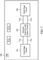
- FIG. 7 depicts a chip 700 comprising a dynamic amplifier 702 in accordance with an exemplary embodiment of the disclosure.
- the dynamic amplifier 702 uses the bypass design of the disclosure.
- the chip 700 further comprises a front-stage circuit 704 and a back-stage circuit 706.
- the front-stage circuit 704 transmits the differential inputs Vip and Vin to the dynamic amplifier 702.
- the chip 700 further comprises a register R_i2 for setting variable bypass currents I 2 provided by the bypass current sources of the dynamic amplifier 702.
- the chip 700 further comprises a register R_Tb for setting the bypass period Tb arranged in the dynamic amplifier 702.
Landscapes
- Engineering & Computer Science (AREA)
- Power Engineering (AREA)
- Amplifiers (AREA)
Abstract
Description
- The present invention relates to dynamic amplifiers.
- In analog electronics, amplifiers are usually used to increase the power of a signal. To minimize power consumption, dynamic amplifiers operating dynamically are introduced. Dynamic amplifiers do not consume static current when amplification is not required. However, the key limitations of dynamic amplifiers include a narrow signal swing when in low-voltage operation. A dynamic amplifier with wide signal swing is called for.
- A dynamic amplifier with bypass design is introduced.
- A dynamic amplifier in accordance with an exemplary embodiment of the disclosure includes an input pair of transistors, a load circuit, a driver for amplification and a bypassing circuit. The input pair of transistors receive a pair of differential inputs Vip and Vin and further provides a first terminal, a second terminal and a third terminal. The load circuit provides a pair of differential outputs Vop and Von with the load circuit coupled to a common mode terminal. The bypassing circuit is operative to decrease currents of the load circuit. The driver is coupled to the first terminal in an amplification phase. In the amplification phase, the load circuit is coupled to the second terminal and the third terminal. The bypassing circuit is coupled to the second terminal and the third terminal during a bypass period within the amplification phase. The dynamic amplifier with bypass design provides a high gain.
- In an exemplary embodiment, the load circuit includes a pair of load capacitor. The pair of load capacitors provides the pair of differential outputs Vop and Von with the load capacitors connected at the common mode terminal. In the amplification phase, the load capacitors are separately coupled to the second terminal and the third terminal
- In an exemplary embodiment, the bypassing circuit includes a pair of bypass current sources operative to decrease currents of the load capacitors. The pair of bypass current sources are separately coupled to the second terminal and the third terminal during the bypass period within the amplification phase.
- In an exemplary embodiment, the driver for amplification is a current source for amplification which is coupled to the first terminal in the amplification phase.
- The bypass current sources may provide variable bypass currents. The bypass period may cover the amplification phase entirely or just partially cover the amplification phase. In some exemplary embodiments, the bypass period is arranged when the amplification phase has been on for a while.
- In some exemplary embodiments, sources of the transistors of the input pair are connected at the first terminal, drains of the transistors of the input pair are regarded as the second terminal and the third terminal, and gates of the transistors of the input pair receive the differential inputs Vin and Vip.
- The amplification phase may end when a predetermined common mode voltage difference, Δ Vcm, for a common mode voltage of the differential outputs Vop and Von is achieved.
- The dynamic amplifier may provides a gain that is equal to gm· Δ Vcm/(I1-I2·Tb/T_A), where gm is the transconductance of each transistor of the input pair, the current source for amplification provides a current of 2·I1, the bypass current sources each provide a bypass current of I2, the amplification phase is T_A long, and the bypass interval is Tb long.
- A detailed description is given in the following embodiments with reference to the accompanying drawings.
- The present invention can be more fully understood by reading the subsequent detailed description and examples with references made to the accompanying drawings, wherein:
-
FIG. 1 depicts adynamic amplifier 100 in accordance with an exemplary embodiment of the disclosure; -
FIG. 2 shows waveforms of the control signals CS_R, CS_A and CSb and depicts the changes of the differential outputs Vop and Von; -
FIG. 3 depicts adynamic amplifier 300 in accordance with another exemplary embodiment of the disclosure; -
FIG. 4 shows waveforms of the control signals CS_R, CS_A and CSb and depicts the changes of the differential outputs Vop and Von with respect to thedynamic amplifier 300; -
FIG. 5 depicts adynamic amplifier 500 in accordance with another exemplary embodiment of the disclosure; -
FIG. 6 shows waveforms of the control signals CS_R/CLK, CS_A and CSb and depicts the changes of the differential outputs Vop and Von with respect to thedynamic amplifier 500; and -
FIG. 7 depicts achip 700 comprising adynamic amplifier 702 in accordance with an exemplary embodiment of the disclosure. - The following description shows exemplary embodiments carrying out the invention. This description is made for the purpose of illustrating the general principles of the invention and should not be taken in a limiting sense. The scope of the invention is best determined by reference to the appended claims.
-
FIG. 1 depicts adynamic amplifier 100 in accordance with an exemplary embodiment of the disclosure, which includes aninput pair 102 of transistors and a pair of load capacitors C1 and C2. A pair of differential inputs Vin and Vip are coupled to thedynamic amplifier 100 by theinput pair 102 of transistors. The load capacitors C1 and C2 connected at a common mode terminal (GND in this example) are used to present the amplified signal on a pair of differential outputs Vop and Von. - The
dynamic amplifier 100 is operated in three phases, including a reset phase, an amplification phase and a sample phase. In the reset phase, the differential outputs Vop and Von are both reset to a predetermined level (short to ground GND in this example). Thedynamic amplifier 100 uses acurrent source 104 to provide a current 2I1 for the amplification phase. Thecurrent source 104 is coupled to the load capacitors C1 and C2 via theinput pair 102 controlled by the differential inputs Vin and Vip. Theinput pair 102 includes three (connection) terminals n1, n2 and n3. As shown, the sources of the transistors forming theinput pair 102 are connected at the connection terminal n1, the drains of the transistors forming theinput pair 102 are regarded as the connection terminals n2 and n3, and the gates of the transistors forming theinput pair 102 are used to receive the differential inputs Vin and Vip. During the amplification phase, the connection terminal n1 is coupled to the firstcurrent source 104 while the connection terminal n2 is coupled to the load capacitor C1 and the connection terminal n3 is coupled to the load capacitor C2. Thus, the voltage levels of the differential outputs Vop and Von change. The amplification phase is ended when a predetermined common mode voltage difference (hereinafter ΔVcm) is made to a common mode voltage of the differential outputs Vop and Von. The sample phase is provided after the amplification phase to sample the differential outputs Vop and Von. - As shown, a pair of bypass
current sources current sources current sources dynamic amplifier 100 has a wide signal swing even in low voltage operation. - In
FIG. 1 , the switches controlled by the control signal CS_R are turned on in the reset phase, the switches controlled by the control signal CS_A are turned on in the amplification phase, and the switches controlled by the control signal CSb are turned on in the bypass period within the amplification phase. The sample phase is arranged after the enable state of the control signal CS_A.FIG. 2 shows waveforms of the control signals CS_R, CS_A and CSb and depicts the changes of the differential outputs Vop and Von. By the control signal CS_R being enabled during the reset phase T_R, the load capacitors C1 and C2 are discharged and the differential outputs Vop and Von are both reset to the ground level. During the amplification phase T_A, charging currents are provided to charge the load capacitors C1 and C2 and the voltage levels of the differential outputs Vop and Von are raised. Before the bypass period Tb, the charging current for each load capacitor (C1 or C2) is I1. Within the bypass period Tb, the charging current for each load capacitor (C1 or C2) is decreased to (I1-I2). The amplification phase T_A ends when the predetermined common mode voltage difference Δ Vcm for the common mode voltage of the differential outputs Vop and Von is achieved. The sample phase T_S is arranged after the amplification phase T_A. The sampling circuit not shown here for the differential outputs Vop and Von may be implemented by any signal sampling design. The gain, G, of thedynamic amplifier 100 is gm·Δ Vcm/(I1-I2·Tb/T_A), where gm is the transconductance of each transistor of theinput pair 102. In comparison with a conventional dynamic amplifier providing a gain of gm·Δ Vcm/I1 without the bypass design, thedynamic amplifier 100 provides a higher gain by the simple bypass design. - In some exemplary embodiments, the
current sources dynamic amplifier 100 has a gain of gm· Δ Vcm/(I1-I2), which is greater than the limited gain, gm·Δ Vcm/I1, provided by a conventional dynamic amplifier. -
FIG. 3 depicts adynamic amplifier 300 in accordance with another exemplary embodiment of the disclosure. In comparison with thedynamic amplifier 100 ofFIG. 1 , the common mode terminal connecting the load capacitors C1 and C2 inFIG. 3 is the power source terminal VDD.FIG. 4 shows waveforms of the control signals CS_R, CS_A and CSb and depicts the changes of the differential outputs Vop and Von with respect to thedynamic amplifier 300. By the control signal CS_R being enabled during the reset phase T_R, the differential outputs Vop and Von are both connected to the power source level (also labeled by VDD). During the amplification phase T_A, currents flow through the load capacitors C1 and C2 to charge the load capacitors C1 and C2 and the voltage levels of the differential outputs Vop and Von are pulled down. In the amplification phase T_A, the current flowing through each load capacitor (C1 or C2) before the bypass period Tb is I1. Within the bypass period Tb, the current flowing through each load capacitor (C1 or C2) is decreased to (I1-I2). The amplification phase ends when the predetermined common mode voltage difference Δ Vcm for the common mode voltage of the differential outputs Vop and Von is achieved. The sample phase T_S is arranged after the amplification phase T_A. The gain, G, of thedynamic amplifier 300 is effectively improved by the bypass design (referring to the bypass currents I2). -
FIG. 5 depicts adynamic amplifier 500 in accordance with another exemplary embodiment of the disclosure. Instead of being discharged, the load capacitors C1 and C2 connected at a common mode terminal GND are pre-charged in the reset phase and discharged in the amplification phase.FIG. 6 shows waveforms of the control signals CS_R, CS_A and CSb and depicts the changes of the differential outputs Vop and Von with respect to thedynamic amplifier 500. By the control signal CS_R enabled during the reset phase T_R, the load capacitors C1 and C2 are pre-charged and the differential outputs Vop and Von are both connected to the power source level VDD. In the amplification phase T_A, discharging currents are provided to discharge the load capacitors C1 and C2 and the voltage levels of the differential outputs Vop and Von drops. Before the bypass period Tb, the discharging current for each load capacitor (C1 or C2) is I1. In the bypass period Tb, the discharging current for each load capacitor (C1 or C2) is decreased to (I1-I2). The amplification phase T_A ends when the predetermined common mode voltage difference Δ Vcm for the common mode voltage of the differential outputs Vop and Von is achieved. The sample phase T_S is arranged after the amplification phase T_A. The gain, G, of thedynamic amplifier 500 is effectively improved by the bypass design (referring to the bypass currents I2). - Any dynamic amplifiers using a bypass design for the pair of load capacitors in the amplification phase are considered within the scope of the disclosure.
- Note that the dynamic amplifiers of the disclosure use switch components and connect the common mode connection terminal to VDD or GND to remove the unnecessary static currents.
- The pair of load capacitors C1 and C2 forming a load circuit may be replaced by other circuits. Any circuit coupled to the common mode terminal and capable of providing the pair of differential outputs Vop and Von can be used to replace the pair of load capacitors C1 and C2 to form the load circuit.
- The current source for amplification (e.g. 104) forming a driver may be replaced by other circuits capable of providing driving capability for signal amplification.
- The pair of bypass
current sources current sources -
FIG. 7 depicts achip 700 comprising adynamic amplifier 702 in accordance with an exemplary embodiment of the disclosure. Thedynamic amplifier 702 uses the bypass design of the disclosure. Thechip 700 further comprises a front-stage circuit 704 and a back-stage circuit 706. The front-stage circuit 704 transmits the differential inputs Vip and Vin to thedynamic amplifier 702. The back-stage circuit 706, receiving the differential outputs Vop and Von from thedynamic amplifier 702. - The
chip 700 further comprises a register R_i2 for setting variable bypass currents I2 provided by the bypass current sources of thedynamic amplifier 702. Thechip 700 further comprises a register R_Tb for setting the bypass period Tb arranged in thedynamic amplifier 702. - While the invention has been described by way of example and in terms of the preferred embodiments, it should be understood that the invention is not limited to the disclosed embodiments. On the contrary, it is intended to cover various modifications and similar arrangements (as would be apparent to those skilled in the art). Therefore, the scope of the appended claims should be accorded the broadest interpretation so as to encompass all such modifications and similar arrangements.
Claims (15)
- A dynamic amplifier, comprising:an input pair of transistors, receiving a pair of differential inputs Vip and Vin and further providing a first terminal (n1), a second terminal (n2) and a third terminal (n3);a load circuit, providing a pair of differential outputs Vop and Von with the load circuit coupled to a common mode terminal;a driver for amplification; anda bypassing circuit, operative to decrease currents of the load circuit,
wherein:the driver is coupled to the first terminal in an amplification phase (T_A);in the amplification phase, the load circuit is coupled to the second terminal and the third terminal; andthe bypassing circuit is coupled to the second terminal and the third terminal during a bypass period (Tb) within the amplification phase. - The dynamic amplifier as claimed in claim 1, wherein:the load circuit includes a pair of load capacitors (C1 and C2);the pair of load capacitors provides the pair of differential outputs Vop and Von with the load capacitors connected at the common mode terminal; andin the amplification phase, the load capacitors are separately coupled to the second terminal and the third terminal.
- The dynamic amplifier as claimed in claim 2, wherein:the bypassing circuit includes a pair of bypass current sources (106 and 108) operative to decrease currents of the load capacitors; andthe pair of bypass current sources are separately coupled to the second terminal and the third terminal during the bypass period within the amplification phase.
- The dynamic amplifier as claimed in claim 3, wherein:the driver for amplification is a current source (104) for amplification which is coupled to the first terminal in the amplification phase.
- The dynamic amplifier as claimed in claim 3, wherein:the bypass current sources provide variable bypass currents.
- The dynamic amplifier as claimed in any one of the preceding claims , wherein:the bypass period is arranged when the amplification phase has been on for a while.
- The dynamic amplifier as claimed in claim 4, wherein:sources of the transistors of the input pair are connected at the first terminal;drains of the transistors of the input pair are regarded as the second terminal and the third terminal; andgates of the transistors of the input pair receive the differential inputs Vin and Vip.
- The dynamic amplifier as claimed in claim 7, wherein:the amplification phase ends when a predetermined common mode voltage difference, Δ Vcm, for a common mode voltage of the differential outputs Vop and Von is achieved;the dynamic amplifier as claimed in claim 10, providing a gain that is equal to gm·Δ Vcm/(I1-I2·Tb/T_A);gm is a transconductance of each transistor of the input pair;the current source for amplification provides a current of 2·I1;the bypass current sources each provide a bypass current of I2;the amplification phase is T_A long; andthe bypass interval is Tb long.
- The dynamic amplifier as claimed in claim 7 or 8, wherein:the load capacitors are discharged in a reset phase (T_R) prior to the amplification phase; andthe load capacitors are charged in the amplification phase.
- The dynamic amplifier as claimed in claim 9, wherein:the common mode terminal is ground;the differential outputs Vop and Von are both pulled down to the ground in the reset phase; andthe differential outputs Vop and Von are raised in the amplification phase.
- The dynamic amplifier as claimed in claim 9, wherein:the common mode terminal is a power source terminal;the differential outputs Vop and Von are both connected to the power source terminal in the reset phase; andthe differential outputs Vop and Von drop in the amplification phase.
- The dynamic amplifier as claimed in claim 7, wherein:the load capacitors are pre-charged in a reset phase (T_R) prior to the amplification phase; andthe load capacitors are discharged in the amplification phase.
- The dynamic amplifier as claimed in claim 12, wherein:the common mode terminal is ground;the differential outputs Vop and Von are both connected to a power source terminal in the reset phase; andthe differential outputs Vop and Von drop in the amplification phase.
- A chip (700), comprising:the dynamic amplifier (702) as claimed in claim 1;a front-stage circuit (704), transmitting the differential inputs Vip and Vin to the dynamic amplifier;a back-stage circuit (706), receiving the differential outputs Vop and Von from the dynamic amplifier; anda register (R_I2) for setting a decreased amount of current that the bypassing circuit caused on the load circuit.
- The chip as claimed in claim 14, further comprising:a register (R_Tb) for arranging the bypass period for the dynamic amplifier.
Applications Claiming Priority (2)
| Application Number | Priority Date | Filing Date | Title |
|---|---|---|---|
| US201662439198P | 2016-12-27 | 2016-12-27 | |
| US15/830,355 US10454435B2 (en) | 2016-12-27 | 2017-12-04 | Dynamic amplifier and chip using the same |
Publications (1)
| Publication Number | Publication Date |
|---|---|
| EP3343765A1 true EP3343765A1 (en) | 2018-07-04 |
Family
ID=60781893
Family Applications (1)
| Application Number | Title | Priority Date | Filing Date |
|---|---|---|---|
| EP17209596.0A Ceased EP3343765A1 (en) | 2016-12-27 | 2017-12-21 | Dynamic amplifier and chip using the same |
Country Status (4)
| Country | Link |
|---|---|
| US (1) | US10454435B2 (en) |
| EP (1) | EP3343765A1 (en) |
| CN (1) | CN108242918B (en) |
| TW (1) | TWI661671B (en) |
Families Citing this family (11)
| Publication number | Priority date | Publication date | Assignee | Title |
|---|---|---|---|---|
| EP3588775A1 (en) * | 2018-06-29 | 2020-01-01 | IMEC vzw | Dynamic amplifier with common mode voltage control |
| WO2021117181A1 (en) * | 2019-12-12 | 2021-06-17 | 日本電信電話株式会社 | Driver circuit |
| CN113315504A (en) * | 2020-02-27 | 2021-08-27 | 成都纳能微电子有限公司 | SST driving structure |
| US11777482B2 (en) * | 2021-05-24 | 2023-10-03 | Mediatek Inc. | Gain-boosted comparator |
| TWI774501B (en) * | 2021-08-04 | 2022-08-11 | 瑞昱半導體股份有限公司 | Charge-steering amplifier-based amplification circuit |
| CN115706568B (en) * | 2021-08-10 | 2025-09-02 | 瑞昱半导体股份有限公司 | Charge-guided amplifier circuit and control method thereof |
| US11569837B1 (en) * | 2021-08-16 | 2023-01-31 | Qualcomm Incorporated | Output common-mode control for dynamic amplifiers |
| US11611318B1 (en) * | 2021-11-17 | 2023-03-21 | Realtek Semiconductor Corp. | Dynamic amplifier of large output swing |
| US12567845B2 (en) | 2022-01-10 | 2026-03-03 | Samsung Electronics Co., Ltd. | Amplifier and electronic system including the same |
| TWI857609B (en) * | 2023-05-15 | 2024-10-01 | 瑞昱半導體股份有限公司 | Amplifier circuit |
| US12445141B2 (en) * | 2023-10-31 | 2025-10-14 | Texas Instruments Incorporated | Voltage-to-delay converter |
Citations (1)
| Publication number | Priority date | Publication date | Assignee | Title |
|---|---|---|---|---|
| US20120313703A1 (en) * | 2011-06-10 | 2012-12-13 | International Business Machines Corporation | Restoring output common-mode of amplifier via capacitive coupling |
Family Cites Families (15)
| Publication number | Priority date | Publication date | Assignee | Title |
|---|---|---|---|---|
| NL8105919A (en) | 1981-12-31 | 1983-07-18 | Philips Nv | DYNAMIC AMPLIFIER CIRCUIT. |
| US5124663A (en) * | 1991-03-04 | 1992-06-23 | Motorola, Inc. | Offset compensation CMOS operational amplifier |
| JP3600175B2 (en) * | 2000-03-23 | 2004-12-08 | 株式会社東芝 | Amplifier and liquid crystal display |
| TWI316332B (en) * | 2004-04-21 | 2009-10-21 | Sony Corp | Differential amplifier device, 2-stage amplifier device, and analog/digital converter device |
| CN101207365B (en) * | 2006-12-20 | 2010-05-19 | 上海华虹Nec电子有限公司 | Gain bootstrap operational amplifier |
| EP2124333B1 (en) * | 2008-05-23 | 2013-01-02 | Zoran Corporation | Comparator circuit |
| JP2010213042A (en) * | 2009-03-11 | 2010-09-24 | Renesas Electronics Corp | Amplifier circuit and analog/digital conversion circuit |
| JP2012039548A (en) | 2010-08-11 | 2012-02-23 | Renesas Electronics Corp | Dynamic amplifier |
| US8610497B2 (en) * | 2011-07-14 | 2013-12-17 | Infineon Technologies Ag | System and method for capacitive signal source amplifier |
| US8493139B2 (en) * | 2011-11-17 | 2013-07-23 | Analog Devices, Inc. | Low noise auto-zero circuits for amplifiers |
| US9379752B2 (en) * | 2012-12-28 | 2016-06-28 | Lattice Semiconductor Corporation | Compensation scheme for MHL common mode clock swing |
| KR102037686B1 (en) * | 2013-04-17 | 2019-10-31 | 에스케이하이닉스 주식회사 | Differential amplifier circuit |
| CN104242879B (en) | 2013-06-20 | 2017-02-08 | 西安电子科技大学 | High-speed low-imbalance dynamic comparator for high-speed analog-digital converter |
| CN103684282A (en) * | 2013-12-24 | 2014-03-26 | 清华大学 | Low-voltage and low-power-consumption amplifier based on nanometer MOS device |
| US9520872B2 (en) * | 2014-12-23 | 2016-12-13 | Qualcomm Incorporated | Linear equalizer with variable gain |
-
2017
- 2017-12-04 US US15/830,355 patent/US10454435B2/en active Active
- 2017-12-14 CN CN201711339660.2A patent/CN108242918B/en active Active
- 2017-12-14 TW TW106143939A patent/TWI661671B/en not_active IP Right Cessation
- 2017-12-21 EP EP17209596.0A patent/EP3343765A1/en not_active Ceased
Patent Citations (1)
| Publication number | Priority date | Publication date | Assignee | Title |
|---|---|---|---|---|
| US20120313703A1 (en) * | 2011-06-10 | 2012-12-13 | International Business Machines Corporation | Restoring output common-mode of amplifier via capacitive coupling |
Non-Patent Citations (3)
| Title |
|---|
| JAMES LIN ET AL: "A 15.5 dB, wide signal swing, dynamic amplifier using a common-mode voltage detection technique", CIRCUITS AND SYSTEMS (ISCAS), 2011 IEEE INTERNATIONAL SYMPOSIUM ON, IEEE, 15 May 2011 (2011-05-15), pages 21 - 24, XP031997561, ISBN: 978-1-4244-9473-6, DOI: 10.1109/ISCAS.2011.5937491 * |
| LIN JAMES ET AL: "An Ultra-Low-Voltage 160 MS/s 7 Bit Interpolated Pipeline ADC Using Dynamic Amplifiers", IEEE JOURNAL OF SOLID-STATE CIRCUITS, IEEE SERVICE CENTER, PISCATAWAY, NJ, USA, vol. 50, no. 6, 1 June 2015 (2015-06-01), pages 1399 - 1411, XP011582284, ISSN: 0018-9200, [retrieved on 20150522], DOI: 10.1109/JSSC.2015.2415472 * |
| VAN DER GOES FRANK ET AL: "A 1.5 mW 68 dB SNDR 80 Ms/s 2 $\times$ Interleaved Pipelined SAR ADC in 28 nm CMOS", IEEE JOURNAL OF SOLID-STATE CIRCUITS, IEEE SERVICE CENTER, PISCATAWAY, NJ, USA, vol. 49, no. 12, 1 December 2014 (2014-12-01), pages 2835 - 2845, XP011564884, ISSN: 0018-9200, [retrieved on 20141120], DOI: 10.1109/JSSC.2014.2361774 * |
Also Published As
| Publication number | Publication date |
|---|---|
| CN108242918B (en) | 2022-03-22 |
| TW201824741A (en) | 2018-07-01 |
| CN108242918A (en) | 2018-07-03 |
| US10454435B2 (en) | 2019-10-22 |
| TWI661671B (en) | 2019-06-01 |
| US20180183394A1 (en) | 2018-06-28 |
Similar Documents
| Publication | Publication Date | Title |
|---|---|---|
| US10454435B2 (en) | Dynamic amplifier and chip using the same | |
| US7839197B2 (en) | Level shift circuit | |
| US7692471B2 (en) | Switched-capacitor circuit having two feedback capacitors | |
| US10594264B2 (en) | Dynamic amplifier and related gain boosting method | |
| US8368453B2 (en) | Switch circuits | |
| US7345530B1 (en) | Regulated switch driving scheme in switched-capacitor amplifiers with opamp-sharing | |
| US9813057B2 (en) | Sampling circuit and sampling method | |
| JP2004140487A (en) | Buffer circuit and driver ic | |
| CN102386862B (en) | There is operational amplifier and the method thereof of overdriving circuit | |
| EP2847868B1 (en) | Inverter-and-switched-capacitor-based squelch detector apparatus and method | |
| US7295042B2 (en) | Buffer | |
| CN103279162A (en) | Low-power-consumption reference voltage buffer based on assembly line ADC | |
| US7372319B1 (en) | Constant boosted voltage generator circuit for feedback switches in a switched capacitor circuit | |
| US11088667B2 (en) | Methods and apparatus for a dual mode operational amplifier | |
| US7301399B2 (en) | Class AB CMOS output circuit equipped with CMOS circuit operating by predetermined operating current | |
| US10784828B2 (en) | Methods and apparatus for an operational amplifier with a variable gain-bandwidth product | |
| US6333673B2 (en) | Electronic circuit | |
| CN111736087B (en) | Power supply detection circuit | |
| US8072274B2 (en) | Oscillation circuit | |
| JP2605603Y2 (en) | Semiconductor integrated circuit | |
| US11595033B2 (en) | Comparator architecture for reduced delay and lower static current | |
| KR20250155889A (en) | Comparator with High Speed and High Energy Efficiency | |
| JPH10107600A (en) | Comparator circuit |
Legal Events
| Date | Code | Title | Description |
|---|---|---|---|
| PUAI | Public reference made under article 153(3) epc to a published international application that has entered the european phase |
Free format text: ORIGINAL CODE: 0009012 |
|
| STAA | Information on the status of an ep patent application or granted ep patent |
Free format text: STATUS: THE APPLICATION HAS BEEN PUBLISHED |
|
| AK | Designated contracting states |
Kind code of ref document: A1 Designated state(s): AL AT BE BG CH CY CZ DE DK EE ES FI FR GB GR HR HU IE IS IT LI LT LU LV MC MK MT NL NO PL PT RO RS SE SI SK SM TR |
|
| AX | Request for extension of the european patent |
Extension state: BA ME |
|
| STAA | Information on the status of an ep patent application or granted ep patent |
Free format text: STATUS: REQUEST FOR EXAMINATION WAS MADE |
|
| 17P | Request for examination filed |
Effective date: 20181219 |
|
| RBV | Designated contracting states (corrected) |
Designated state(s): AL AT BE BG CH CY CZ DE DK EE ES FI FR GB GR HR HU IE IS IT LI LT LU LV MC MK MT NL NO PL PT RO RS SE SI SK SM TR |
|
| STAA | Information on the status of an ep patent application or granted ep patent |
Free format text: STATUS: EXAMINATION IS IN PROGRESS |
|
| 17Q | First examination report despatched |
Effective date: 20190418 |
|
| STAA | Information on the status of an ep patent application or granted ep patent |
Free format text: STATUS: THE APPLICATION HAS BEEN REFUSED |
|
| 18R | Application refused |
Effective date: 20191126 |