EP3343664A1 - Organic light emitting device - Google Patents
Organic light emitting device Download PDFInfo
- Publication number
- EP3343664A1 EP3343664A1 EP17211029.8A EP17211029A EP3343664A1 EP 3343664 A1 EP3343664 A1 EP 3343664A1 EP 17211029 A EP17211029 A EP 17211029A EP 3343664 A1 EP3343664 A1 EP 3343664A1
- Authority
- EP
- European Patent Office
- Prior art keywords
- light emitting
- organic light
- electrode
- emitting device
- emitting layer
- Prior art date
- Legal status (The legal status is an assumption and is not a legal conclusion. Google has not performed a legal analysis and makes no representation as to the accuracy of the status listed.)
- Granted
Links
Images






Classifications
-
- H—ELECTRICITY
- H10—SEMICONDUCTOR DEVICES; ELECTRIC SOLID-STATE DEVICES NOT OTHERWISE PROVIDED FOR
- H10K—ORGANIC ELECTRIC SOLID-STATE DEVICES
- H10K50/00—Organic light-emitting devices
- H10K50/80—Constructional details
- H10K50/805—Electrodes
- H10K50/81—Anodes
- H10K50/813—Anodes characterised by their shape
-
- H—ELECTRICITY
- H10—SEMICONDUCTOR DEVICES; ELECTRIC SOLID-STATE DEVICES NOT OTHERWISE PROVIDED FOR
- H10K—ORGANIC ELECTRIC SOLID-STATE DEVICES
- H10K59/00—Integrated devices, or assemblies of multiple devices, comprising at least one organic light-emitting element covered by group H10K50/00
- H10K59/80—Constructional details
- H10K59/805—Electrodes
- H10K59/8052—Cathodes
- H10K59/80521—Cathodes characterised by their shape
-
- H—ELECTRICITY
- H10—SEMICONDUCTOR DEVICES; ELECTRIC SOLID-STATE DEVICES NOT OTHERWISE PROVIDED FOR
- H10K—ORGANIC ELECTRIC SOLID-STATE DEVICES
- H10K50/00—Organic light-emitting devices
- H10K50/10—OLEDs or polymer light-emitting diodes [PLED]
- H10K50/11—OLEDs or polymer light-emitting diodes [PLED] characterised by the electroluminescent [EL] layers
-
- H—ELECTRICITY
- H10—SEMICONDUCTOR DEVICES; ELECTRIC SOLID-STATE DEVICES NOT OTHERWISE PROVIDED FOR
- H10K—ORGANIC ELECTRIC SOLID-STATE DEVICES
- H10K50/00—Organic light-emitting devices
- H10K50/80—Constructional details
- H10K50/805—Electrodes
- H10K50/82—Cathodes
- H10K50/822—Cathodes characterised by their shape
-
- H—ELECTRICITY
- H10—SEMICONDUCTOR DEVICES; ELECTRIC SOLID-STATE DEVICES NOT OTHERWISE PROVIDED FOR
- H10K—ORGANIC ELECTRIC SOLID-STATE DEVICES
- H10K50/00—Organic light-emitting devices
- H10K50/80—Constructional details
- H10K50/85—Arrangements for extracting light from the devices
-
- H—ELECTRICITY
- H10—SEMICONDUCTOR DEVICES; ELECTRIC SOLID-STATE DEVICES NOT OTHERWISE PROVIDED FOR
- H10K—ORGANIC ELECTRIC SOLID-STATE DEVICES
- H10K59/00—Integrated devices, or assemblies of multiple devices, comprising at least one organic light-emitting element covered by group H10K50/00
- H10K59/10—OLED displays
-
- H—ELECTRICITY
- H10—SEMICONDUCTOR DEVICES; ELECTRIC SOLID-STATE DEVICES NOT OTHERWISE PROVIDED FOR
- H10K—ORGANIC ELECTRIC SOLID-STATE DEVICES
- H10K59/00—Integrated devices, or assemblies of multiple devices, comprising at least one organic light-emitting element covered by group H10K50/00
- H10K59/10—OLED displays
- H10K59/12—Active-matrix OLED [AMOLED] displays
- H10K59/121—Active-matrix OLED [AMOLED] displays characterised by the geometry or disposition of pixel elements
- H10K59/1213—Active-matrix OLED [AMOLED] displays characterised by the geometry or disposition of pixel elements the pixel elements being TFTs
-
- H—ELECTRICITY
- H10—SEMICONDUCTOR DEVICES; ELECTRIC SOLID-STATE DEVICES NOT OTHERWISE PROVIDED FOR
- H10K—ORGANIC ELECTRIC SOLID-STATE DEVICES
- H10K59/00—Integrated devices, or assemblies of multiple devices, comprising at least one organic light-emitting element covered by group H10K50/00
- H10K59/10—OLED displays
- H10K59/12—Active-matrix OLED [AMOLED] displays
- H10K59/122—Pixel-defining structures or layers, e.g. banks
-
- H—ELECTRICITY
- H10—SEMICONDUCTOR DEVICES; ELECTRIC SOLID-STATE DEVICES NOT OTHERWISE PROVIDED FOR
- H10K—ORGANIC ELECTRIC SOLID-STATE DEVICES
- H10K59/00—Integrated devices, or assemblies of multiple devices, comprising at least one organic light-emitting element covered by group H10K50/00
- H10K59/10—OLED displays
- H10K59/12—Active-matrix OLED [AMOLED] displays
- H10K59/123—Connection of the pixel electrodes to the thin film transistors [TFT]
-
- H—ELECTRICITY
- H10—SEMICONDUCTOR DEVICES; ELECTRIC SOLID-STATE DEVICES NOT OTHERWISE PROVIDED FOR
- H10K—ORGANIC ELECTRIC SOLID-STATE DEVICES
- H10K59/00—Integrated devices, or assemblies of multiple devices, comprising at least one organic light-emitting element covered by group H10K50/00
- H10K59/10—OLED displays
- H10K59/12—Active-matrix OLED [AMOLED] displays
- H10K59/124—Insulating layers formed between TFT elements and OLED elements
-
- H—ELECTRICITY
- H10—SEMICONDUCTOR DEVICES; ELECTRIC SOLID-STATE DEVICES NOT OTHERWISE PROVIDED FOR
- H10K—ORGANIC ELECTRIC SOLID-STATE DEVICES
- H10K59/00—Integrated devices, or assemblies of multiple devices, comprising at least one organic light-emitting element covered by group H10K50/00
- H10K59/30—Devices specially adapted for multicolour light emission
- H10K59/38—Devices specially adapted for multicolour light emission comprising colour filters or colour changing media [CCM]
-
- H—ELECTRICITY
- H10—SEMICONDUCTOR DEVICES; ELECTRIC SOLID-STATE DEVICES NOT OTHERWISE PROVIDED FOR
- H10K—ORGANIC ELECTRIC SOLID-STATE DEVICES
- H10K59/00—Integrated devices, or assemblies of multiple devices, comprising at least one organic light-emitting element covered by group H10K50/00
- H10K59/80—Constructional details
- H10K59/805—Electrodes
- H10K59/8051—Anodes
- H10K59/80515—Anodes characterised by their shape
-
- H—ELECTRICITY
- H10—SEMICONDUCTOR DEVICES; ELECTRIC SOLID-STATE DEVICES NOT OTHERWISE PROVIDED FOR
- H10K—ORGANIC ELECTRIC SOLID-STATE DEVICES
- H10K59/00—Integrated devices, or assemblies of multiple devices, comprising at least one organic light-emitting element covered by group H10K50/00
- H10K59/80—Constructional details
- H10K59/805—Electrodes
- H10K59/8051—Anodes
- H10K59/80518—Reflective anodes, e.g. ITO combined with thick metallic layers
-
- H—ELECTRICITY
- H10—SEMICONDUCTOR DEVICES; ELECTRIC SOLID-STATE DEVICES NOT OTHERWISE PROVIDED FOR
- H10K—ORGANIC ELECTRIC SOLID-STATE DEVICES
- H10K59/00—Integrated devices, or assemblies of multiple devices, comprising at least one organic light-emitting element covered by group H10K50/00
- H10K59/80—Constructional details
- H10K59/875—Arrangements for extracting light from the devices
- H10K59/878—Arrangements for extracting light from the devices comprising reflective means
-
- H—ELECTRICITY
- H10—SEMICONDUCTOR DEVICES; ELECTRIC SOLID-STATE DEVICES NOT OTHERWISE PROVIDED FOR
- H10K—ORGANIC ELECTRIC SOLID-STATE DEVICES
- H10K2101/00—Properties of the organic materials covered by group H10K85/00
-
- H—ELECTRICITY
- H10—SEMICONDUCTOR DEVICES; ELECTRIC SOLID-STATE DEVICES NOT OTHERWISE PROVIDED FOR
- H10K—ORGANIC ELECTRIC SOLID-STATE DEVICES
- H10K2102/00—Constructional details relating to the organic devices covered by this subclass
-
- H—ELECTRICITY
- H10—SEMICONDUCTOR DEVICES; ELECTRIC SOLID-STATE DEVICES NOT OTHERWISE PROVIDED FOR
- H10K—ORGANIC ELECTRIC SOLID-STATE DEVICES
- H10K2102/00—Constructional details relating to the organic devices covered by this subclass
- H10K2102/10—Transparent electrodes, e.g. using graphene
- H10K2102/101—Transparent electrodes, e.g. using graphene comprising transparent conductive oxides [TCO]
- H10K2102/102—Transparent electrodes, e.g. using graphene comprising transparent conductive oxides [TCO] comprising tin oxides, e.g. fluorine-doped SnO2
-
- H—ELECTRICITY
- H10—SEMICONDUCTOR DEVICES; ELECTRIC SOLID-STATE DEVICES NOT OTHERWISE PROVIDED FOR
- H10K—ORGANIC ELECTRIC SOLID-STATE DEVICES
- H10K2102/00—Constructional details relating to the organic devices covered by this subclass
- H10K2102/10—Transparent electrodes, e.g. using graphene
- H10K2102/101—Transparent electrodes, e.g. using graphene comprising transparent conductive oxides [TCO]
- H10K2102/103—Transparent electrodes, e.g. using graphene comprising transparent conductive oxides [TCO] comprising indium oxides, e.g. ITO
-
- H—ELECTRICITY
- H10—SEMICONDUCTOR DEVICES; ELECTRIC SOLID-STATE DEVICES NOT OTHERWISE PROVIDED FOR
- H10K—ORGANIC ELECTRIC SOLID-STATE DEVICES
- H10K2102/00—Constructional details relating to the organic devices covered by this subclass
- H10K2102/301—Details of OLEDs
- H10K2102/351—Thickness
-
- H—ELECTRICITY
- H10—SEMICONDUCTOR DEVICES; ELECTRIC SOLID-STATE DEVICES NOT OTHERWISE PROVIDED FOR
- H10K—ORGANIC ELECTRIC SOLID-STATE DEVICES
- H10K50/00—Organic light-emitting devices
- H10K50/80—Constructional details
- H10K50/85—Arrangements for extracting light from the devices
- H10K50/854—Arrangements for extracting light from the devices comprising scattering means
-
- H—ELECTRICITY
- H10—SEMICONDUCTOR DEVICES; ELECTRIC SOLID-STATE DEVICES NOT OTHERWISE PROVIDED FOR
- H10K—ORGANIC ELECTRIC SOLID-STATE DEVICES
- H10K59/00—Integrated devices, or assemblies of multiple devices, comprising at least one organic light-emitting element covered by group H10K50/00
- H10K59/80—Constructional details
- H10K59/875—Arrangements for extracting light from the devices
- H10K59/877—Arrangements for extracting light from the devices comprising scattering means
Definitions
- the present disclosure relates to an organic light emitting diode and an organic light emitting device that emits light.
- An organic light emitting device has advantages in that by using self-light emitting Organic Light Emitting Diodes (OLEDs), a response speed is high, a light emitting efficiency is high, a luminance is high, and a viewing angle is wide.
- OLEDs Organic Light Emitting Diodes
- An organic light emitting layer of the organic light emitting device passes through various elements of the organic light emitting device, and is emitted from the organic light emitting device.
- some light, which is emitted from the organic light emitting layer is confined inside the organic light emitting diode device, rather than being emitted from the organic light emitting device. Therefore, the light extraction efficiency of the organic light emitting device becomes an issue.
- a method of attaching a Micro Lens Array (MLA) to the outside of a substrate of the organic light emitting device has been used in order to improve the light extraction efficiency of the organic light emitting device.
- MLA Micro Lens Array
- an object of the present disclosure is to provide an organic light emitting diode and an organic light emitting device that improve an outward light emitting efficiency and reduce power consumption.
- An exemplary embodiment may provide an organic light emitting diode that includes a first electrode including at least one curved part, an organic light emitting layer disposed on the first electrode, and a second electrode disposed on the organic light emitting layer. Further, the exemplary embodiment may provide an organic light emitting device including the organic light emitting diode. That is, the first electrode may include at least one concave part (e.g. an indentation) and/or at least one convex part (e.g. a protrusion). Thus, the first electrode may have a corrugated surface. 17
- the concave part may include a concave bottom. or The convex part may include a convex top.
- the concave part and/or the convex part may include one or more inclined side surfaces.
- a first thickness of the organic light emitting layer adjacent to said one or more of the inclined side surfaces is thinner than a second thickness of the organic light emitting layer adjacent to the concave bottom or the convex top.
- the first thickness may be thinner than the second thickness by 15%-50% of the second thickness.
- An inclined side surface of the concave part of the first electrode may form an acute angle with a bottom surface of the concave part of the first electrode.
- An inclined side surface of the the convex part of the first electrode may form an acute angle with a top surface of the convex part of the first electrode.
- the acute angle may range from 15 degrees to 70 degrees.
- the organic light emitting layer may have a thickness that is thinnest on the inclined side surface of the first electrode.
- a first thickness of the organic light emitting layer on the inclined side surface of the first electrode may be thinner than a second thickness of the organic light emitting layer on the bottom surface of the concave part of the first electrode by 15%-50% of the second thickness.
- a first thickness of the organic light emitting layer on the inclined side surface of the first electrode may be thinner than a second thickness of the organic light emitting layer on the top surface of the convex part of the first electrode by 15%-50% of the second thickness.
- the organic light emitting layer and the second electrode may be arranged following a shape of a top surface of the first electrode.
- the first electrode may include an amorphous metal oxide.
- the amorphous metal oxide may include at least one selected from a group consisting of Indium Zinc Oxide (IZO), Zinc Tin Oxide (ZTO), SnO2 (tin oxide), ZnO (zinc oxide), In2O3 (indium oxide), Gallium Indium Tin Oxide (GITO), Indium Gallium Zinc Oxide (IGZO), Zinc Indium Tin Oxide (ZITO), Indium Gallium Oxide (IGO), Ga2O3 (gallium oxide), Aluminum Zinc Oxide (AZO), and Gallium Zinc Oxide (GZO).
- IZO Indium Zinc Oxide
- ZTO Zinc Tin Oxide
- SnO2 tin oxide
- ZnO zinc oxide
- In2O3 indium oxide
- GITO Gallium Indium Tin Oxide
- IGZO Indium Zin
- the first electrode may include the concave part together with another concave part and a connection part that is disposed between the concave part and said another concave part.
- the connection part may be flat.
- the organic light emitting device may further comprise a substrate; a thin film transistor on the substrate; and one or more insulation layers on the thin film transistor, the first electrode disposed on the one or more insulation layers and electrically connected to the thin film transistor through the one or more insulation layers.
- the organic light emitting device may further comprise a color filter disposed in or on the one or more insulation layers to overlap with at least a part of the organic light emitting layer.
- a concave bottom of the concave part may be in contact with the one or more insulation layers.
- a concave bottom of the concave part may be disposed over the one or more insulation layers with a gap therebetween.
- a concave bottom of the concave part may be flat.
- a concave bottom of the concave part may be pointy to form an angle with a surface of the one or more insulation layers.
- the concave part and/or the convex part may have a three-dimensionally tapered shape, i.e. a conical shape.
- the concave part and/or the convex part may have a cross-section of one of a circular shape, a hemispherical shape, a semi-ellipsoidal shape, a square shape, and a hexagonal shape.
- cross-section may refer to a section parallel to the connection part, or parallel to a substrate on which the first electrode is formed.
- an organic light emitting diode and an organic light emitting device that can improve an external light emitting efficiency and can reduce power consumption.
- first, second, A, B, (a), (b) or the like may be used herein when describing components of the present disclosure.
- Each of these terminologies is not used to define an essence, order or sequence of a corresponding component but used merely to distinguish the corresponding component from other component(s).
- another structural element may "be connected to", “be coupled to”, or “be in contact with” the structural elements as well as that the certain structural element is directly connected to or is in direct contact with another structural element.
- FIG. 1 is a cross-sectional view of an organic light emitting diode according to one exemplary embodiment.
- an organic light emitting diode 10 includes a first electrode 41 including a concave part or a convex part, an organic light emitting layer 42 disposed on the first electrode 41, and a second electrode 43 disposed on the organic light emitting layer 42.
- a structure and a shape of the organic light emitting diode 10 will be made later with reference to FIGS. 3A , 3B , and 10 .
- FIG. 2 is a cross-sectional view of an organic light emitting device according to one exemplary embodiment.
- FIG. 3A is an enlarged cross-sectional view for the region "X" in FIG. 2 .
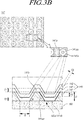
- FIG. 3B illustrates a plan view of the first electrode of FIG. 2 and an enlarged sectional view of the region "X" of FIG. 2 , which corresponds to the planar structure of the first electrode.
- an organic light emitting device 100 may be any of various light emitting devices that include an organic light emitting diode or an organic electric element including two electrodes and an organic layer between the two electrodes.
- the organic light emitting device 100 may be one of an organic light emitting display device that displays an image, a lighting device, and a light source.
- the organic light emitting device 100 when the organic light emitting device 100 is an organic light emitting diode display device, it may be, but not exclusively, at least one of a bottom emission display device, a top emission display device, a dual emission display device, a flexible display device, and a tranparent display device.
- the organic light emitting device 100 When the organic light emitting device 100 is a lighting device, it may be an indoor or outdoor lighting device, a vehicular lighting device, or the like, or may be combined with another mechanical member to be applied to the above-described lighting devices.
- the vehicular lighting device may be, but not exclusively, at least one of a head lamp, a high beam lamp, a tail lamp, a brake lamp, a back light, a stop lamp, a fog lamp, a turn signal light, and an auxiliary lamp.
- the organic light emitting device 100 When the organic light emitting device 100 is a light source, it may be efficiently applied to, for example: a light source of a backlight of a Liquid Crystal Display (LCD), various lighting sensors, a printer, or a copying machine; a light source of a vehicle instrument; a light source of a signal lamp, a sign lamp, or a surface light emitting body; a decoration; various lights; or the like.
- LCD Liquid Crystal Display
- the organic light emitting device 100 is an organic light emitting diode display device.
- the organic light emitting device 100 may be a lighting device or a light source.
- the organic light emitting device 100 is illustrated as including a substrate 110, a thin film transistor 120, a color filter 150, a third insulation layer 160, and an organic light emitting diode 140, but is not limited thereto.
- the organic light emitting device 100 may be an organic light emitting device including an organic light emitting diode 140 on the substrate 110, and may be an organic light emitting device including a third insulation layer 160 on the substrate 110, and an organic light emitting diode 140 on the third insulation layer 160.
- the third insulation layer 160 may be disposed under the first electrode 141 of the organic light emitting diode 140, and may be a flat insulation layer.
- the organic light emitting device 100 illustrated in FIGS. 2 and 3A is a bottom emission type organic light emitting device.
- the organic light emitting device 100 according to an exemplary embodiment may be a top emission type organic light emitting device.
- the thin film transistor 120 is disposed, which includes a gate electrode 121, an active layer 122, a source electrode 123, and a drain electrode 124. More specifically, the gate electrode 121 is disposed on the substrate 110, a first insulation layer 131 for insulating the gate electrode 121 and the active layer 122 is formed on the gate electrode 121 and the substrate 110, and the active layer 122 is disposed on the first insulation layer 131. Further, an etch stopper 132 is disposed on the active layer 122, and the source electrode 123 and the drain electrode 124 are disposed on the active layer 122 and the etch stopper 132.
- the source electrode 123 and the drain electrode 124 are electrically connected with the active layer 122 in a manner of being in contact with the active layer 122, and are disposed on a partial region of the etch stopper 132. In some embodiments, the etch stopper 132 may not be provided.
- the thin film transistor 120 has a bottom gate structure or an inverted staggered structure in which the gate electrode 121 is located on the opposite side of the source electrode 123 and the drain electrode 124 with reference to the active layer 122.
- a thin film transistor 120 having a coplanar structure or a top gate structure may also be used, in which the gate electrode 121 is positioned at the same side as the source electrode 123 and the drain electrode 124 with reference to the active layer 122.
- a second insulation layer 133 is disposed on the thin film transistor 120, and a color filter 150 is disposed on the second insulation layer 133.
- FIG. 2 illustrates that the second insulation layer 133 flattens the top portion of the thin film transistor 120.
- the second insulation layer 133 may be disposed following the surface shapes of the elements positioned therebelow, rather than flattening the top portion of the thin film transistor 120.
- the color filter 150 is configured to convert the color of light emitted from the organic light emitting layer 142, and may be one of, for example, a red color filter, a green color filter, and a blue color filter.
- the color filter 150 is disposed on the second insulation layer 133 at a position corresponding to a light emitting region.
- the light emitting region means a region where the organic light emitting layer 142 emits light by the first electrode 141 and the second electrode 143.
- the description "the color filter 150 is disposed at a position corresponding to the light emitting region” means that the color filter 150 is disposed to prevent blurring and ghost phenomena from occurring due to a mutual mixing of lights emitted from neighboring light emitting regions.
- the color filter 150 is arranged to be superimposed on the light emitting region. More specifically, the color filter 150 may have a size that is smaller than the light emitting region. However, the disposed position and size of the color filter 150 may be determined by various factors, such as a distance between the color filter 150 and the first electrode 141 and a distance between the color filter 150 and the third insulation layer 160 and a distance between a light emitting region and a non-light emitting region, in addition to the size and position of the light emitting region.
- the third insulation layer 160 is disposed on the color filter 150 and the second insulation layer 133.
- FIG. 2 illustrates that the second insulation layer 133 is included in the organic light emitting device 100, in other embodiments the third insulation layer 160 may be directly disposed on the thin film transistor 120 without using the second insulation layer 133.
- FIG. 2 illustrates that the color filter 150 is disposed on the second insulation layer 133, the color filter 150 may be disposed at any position between the third insulation layer 160 and the substrate 110 without being limited thereto.
- a bank layer 136 and the organic light emitting diode 140 including the first electrode 141, the organic light emitting layer 142, and the second electrode 143 are disposed on the third insulation layer 160.
- an insulative second insulation layer (not illustrated), which has a refractive index similar to that of the first electrode 141, may be added between the third insulation layer 160 and the first electrode 141 to block outgassing from the third insulation layer 160 from spreading to the organic light emitting diode 140.
- the first electrode 141 is disposed on the third insulation layer 160 to supply electrons or holes to the organic light emitting layer 142.
- the first electrode 141 may be a positive pole, a pixel electrode, or an anode in a normal organic light emitting diode (OLED), and may be a negative pole, a pixel electrode, or a cathode in an inverted OLED.
- the first electrode 141 may be connected to the source electrode 123 of the thin film transistor 120 through contact holes formed in the third insulation layer 160 and the second insulation layer 133.
- the first electrode 141 is connected to the source electrode 123 on the assumption that the thin film transistor 120 is an N-type thin film transistor.
- the first electrode 141 may be connected to the drain electrode 124.
- the first electrode 141 may be directly in contact with the organic light emitting layer 142, or may be in contact with the organic light emitting layer 142 with a conductive material being interposed therebetween so that the first electrode 141 can be electrically connected to the organic light emitting layer 142.
- the first electrode 141 may be a single layer, but may be a multilayer including two or more layers.
- the first electrode 141 includes concave parts 141a and a first connection part 141b connecting neighboring concave parts 141a.
- the first electrode 141 is flat in a part where no concave part 141 a is disposed. That is, the first connection part 141 b is flat or plane.
- FIG. 3A although it is illustrated that a plurality of concave parts 141a are provided. However, for example, a single concave part 141a may be provided without being limited thereto.
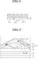
- FIG. 4 is a partial perspective view illustrating the third insulation layer and the first electrode of FIG. 2 partially in cross section.
- the concave part 141a may have a shape inclined to be narrowed downward.
- the concave part 141a may include at least one inclined surface 141aa and a bottom 141ab.
- the bottom 141ab may be flat and/or parallel to the first connection part 141b.
- the bottom 141ab of the concave part 141a may be surrounded by the inclined surface 141aa.
- the inclined surface 141aa may be located between the bottom 141ab and the first connection part 141b.
- the concave part 141a may be symmetric, e.g. with respect to a line perpendicular to the first connection part 141b.
- the concave part 141a may have a constant taper shape.
- the cross-sectional shape of the concave part 141a may be a trapezoidal shape, but is not limited thereto.
- the concave part 141 a may have a larger width on a level with the first connection part 141b than on a level with the bottom 141ab.
- the inclination ⁇ of the inclined surface 141aa of the concave part 141 a means an angle formed by the inclined surface 141 aa of the concave part 141 a and a bottom surface of the first electrode 141.
- the bottom surface of the first electrode 141 may refer to a surface of the first electrode that is in contact with an insulation layer, i.e. to a surface that is not in contact with the organic light emitting layer 142.
- the inclination ⁇ may be an acute angle. That is, the bottom surface of the first electrode 141 may be flat or plane, e.g. parallel to the surface of the first connection part 141b or to the substrate 110.
- FIG. 3B illustrates that the inclined surface 141aa of the concave part 141a is linear in a cross section
- FIG. 4 illustrates that the inclined surface 141aa of the concave part 141a is flat.
- the inclined surface 141aa of the concave part 141a may be generally linear or planar, although it may include a non-linear or curved surface in a cross section.
- the inclination ⁇ of the inclined surface 141aa of the concave part 141 a may be 15 to 70 degrees.
- the light extraction efficiency may be weak.
- the traveling angle of light, which starts to travel from an effective light emitting region may be 42 degrees or more. Consequently, the light may be confined again inside the organic light emitting diode 140 and the light emitting efficiency may not be increased.
- the separation distance G (gap) at the bottom 141ab of the concave part 141a or rather a width of the bottom 141ab is larger than 0, the separation distance G (gap), i.e. the smallest interval between two oppsite portions of the inclined surface 141aa of one concave part 141a or the width of the bottom 141ab of the concave part 141a, may be zero (i.e., two facing portions of the inclined surfaces 141aa of the concave part 141a may be adjacent to each other without a gap G, i.e.
- the concave part 141a may have a triangular cross-section, rather than a trapezoidal one), as will be described later with reference to FIG. 8A .
- the bottom 141ab of the concave part 141a is open, i.e. that the first electrode 141 exposes the organic light emitting layer 142 at bottoms 141ab of the concave parts 141a, material of the first electrode 141 may be present at the bottoms 141ab of the concave parts 141 a.
- the concave parts 141a may have a circular shape as a whole in a plan view, i.e. in a plane parallel to the substrate 110 or in a plane parallel to the first connection part 141 b or the bottoms 141 ab of the concave parts.
- the concave parts 141a may have various shapes, such as a hemispherical shape, a semi-ellipsoidal shape, a square shape, and a hexagonal shape.
- the shape of the concave parts 141 a of the first electrode 141 is formed through the processes, such as photolithography, wet etching, and dry etching. In this case, the morphology of the concave parts 141a of the first electrode 141 can be adjusted when a heat treatment process performed at this time is adjusted.
- the first electrode 141 may include an amorphous metal oxide.
- the amorphous metal oxide may include any one selected from a group consisting of Indium Zinc Oxide (IZO), Zinc Tin Oxide (ZTO), SnO2 (tin oxide), ZnO (zinc oxide), In2O3 (indium oxide), Gallium Indium Tin Oxide (GITO), Indium Gallium Zinc Oxide (IGZO), Zinc Indium Tin Oxide (ZITO), Indium Gallium Oxide (IGO), Ga2O3 (gallium oxide), Aluminum Zinc Oxide (AZO) and Gallium Zinc Oxide (GZO).
- IZO Indium Zinc Oxide
- ZTO Zinc Tin Oxide
- SnO2 tin oxide
- ZnO zinc oxide
- In2O3 indium oxide
- GITO Gallium Indium Tin Oxide
- IGZO Indium Gallium Zinc Oxide
- ZITO Zinc Indium Tin Oxide
- IGO Indium Gallium Oxide
- the first electrode 141 When the first electrode 141 includes the amorphous metal oxide, it may be suitable for forming the concave portion 141a of the first electrode 141 to the three-dimensionally constant taper shape through processes such as photolithography, wet etching, and dry etching. In terms of material-process relationship, it is possible to form the concave portion 141a of the first electrode 141 to a three-dimensionally reverse taper shape if the material of the first electrode 141 is selected incorrectly.
- a bank layer 136 is disposed on the third insulation layer 160 and the first electrode 141, and the bank layer 136 includes an opening 136a that exposes the first electrode 141.
- the bank layer 136 serves to separate neighboring pixels (or sub-pixels) regions, and may be disposed between neighboring pixel (or sub-pixel) regions.
- the concave parts 141a and the first connection part 141b of the first electrode 141 are disposed to be superimposed on the opening 136a of the bank layer 136.
- the organic light emitting layer 142 is disposed on the first electrode 141, and the second electrode 143 is disposed on the organic light emitting layer 142 to supply electrons or holes to the organic light emitting layer 142.
- the organic light emitting layer 142 is disposed in a tandem white structure in which a plurality of organic light emitting layers are stacked in order to emit white light.
- the organic light emitting layer 142 may include a first organic light emitting layer that emits blue light and a second organic light emitting layer that is disposed on the first organic light emitting layer and emits light having a color that becomes white when mixed with blue.
- the second organic light emitting layer may be an organic light emitting layer that emits, for example, yellow green light.
- the organic light emitting layer 142 may only include an organic light emitting layer that emits one of blue light, red light, and green light.
- the color filter 150 may not be included.
- the second electrode 143 may be a negative pole, a common electrode, or a cathode in a normal organic light emitting diode (OLED), and may be a positive pole, a common electrode, or an anode in an inverted OLED.
- the organic light emitting layer 142 and the second electrode 143 are disposed in a shape that follows the morphology of the top surface of the first electrode 141. Accordingly, the organic light emitting layer 142 and the second electrode 143 have a concave morphology in the concave parts 141 a of the first electrode 141. Consequently, the shape of the organic light emitting diode 140 may be implemented using the concave parts 141 a of the first electrode 141. In other words, the organic light emitting diode 140 may be configured with indentations corresponding to the concave parts 141 a of the first electrode 141.
- a thickness of the organic light emitting layer 142 in a direction perpendicular to a surface of the first electrode 141 may be relatively thin in a region corresponding to the inclined surface 141aa of the concave part 141a.
- a thickness T3 of the organic light emitting layer 142in a region corresponding to the inclined surface 141aa of the concave part 141 a may be thinner than a thickness T2 of the organic light emitting layer 142in a region corresponding to the bottom 141ab of the concave part 141a and/or a thickness T1 of the organic light emitting layer 142 in a region corresponding to the first connection part 141b of the first electrode 141, i.e. T3 ⁇ T1, T2 (see Fig. 3B ).
- the thicknesses T1, T2, and T4 of the organic light emitting layer 142 deposited in a direction perpendicular to the substrate 110 are about the same.
- the thickness T3 of the organic light emitting layer 142 in vertical direction to the inclined surface of the organic light emitting layer 142 driving a current between the first and second electrodes 141 and 143 becomes relatively thin.
- the thicknesses T1 and T2 of the organic light emitting layer 142 in regions corresponding to the bottom 141ab of the concave part 141a and to the first connection part 141b driving a current between the first electrode 141 and the second electrode 143 are relatively thick.
- the thickness T3 of the organic light emitting layer 142 which is perpendicular to the first electrode 141 in the region corresponding to the inclined surface 141aa of each concave part 141 a, is reduced as the inclination ⁇ of the inclined surface 141aa of the concave part 141a is increased.
- the thickness T3 of the organic light emitting layer 142, which is perpendicular to the first electrode 141 in the region corresponding to the inclined surface 141aa of each concave part 141 a, and the inclination ⁇ of the inclined surface 141aa of the concave part 141a are determined according to Equation 1 as follows.
- the thickness of the organic light emitting layer 142 in a region corresponding to the inclined surface 141aa of each concave part 141a may be relatively thinner than the part of the thickness of the organic light emitting layer 142 adjacent to the bottom 141ab of the concave part 141a or the first connection part 141b of the first electrode 141.
- the thickness of the organic light emitting layer 142 in a region corresponding to the inclined surface 141aa of each concave part 141 a being relatively thin may result in an efficient light emitting region in which electric fields are locally concentrated.
- electric fields are locally concentrated in the efficient light emitting region, and a main current path is formed to generate the main light emission.
- T3 is a value of T1 reduced by 15%-50%, T2 reduced by 15%-50%, or T4 reduced by 15%-50%.
- T3 is T1 (or T2, or T4) reduced by less than 15%, light emission quantity is not enhanced significantly.
- T3 is T1 (or T2, or T4) reduced by more than 50%, light emission quantity may be significantly enhanced but the organic light emitting layer 142 is so thin that the life of the organic light emitting device 100 may be deteriorated. Therefore, the organic light emitting layer 142 is made to have a thickness of T3 thinner than T1 or T2 or T4 by a modest amount (i.e., 50% - 85% of T1 or T2 or T4, i.e. T1 or T2 or T4 reduced by 15%-50%) to achieve enhancement of light emission and life of the organic light emitting device at the same time.
- the light emission quantity per unit area of the organic light emitting layer 142 in the inclined surface 141aa between the bottom 141ab of the concave part 141a and the first connection part 141b of the first electrode 141 may be larger than the light emission quantity per unit area of the organic light emitting layer 142 in the bottom 141 ab of the concave part 141 a or the first connection part 141b.
- FIG. 5 is an enlarged cross-sectional view of a part of the region "X" in FIG. 2 , illustrating optical paths of light emitted from an organic light emitting layer.
- the light emitted from the organic light emitting layer 142 which is confined by being totally reflected in the first electrode 141 and the organic light emitting layer 142, is extracted to the outside by being re-reflected from the second electrode 143 positioned to correspond to the inclined surface 141aa by the concave structure of the first electrode 141, so that outward light emitting efficiency can be improved.
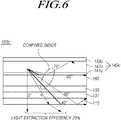
- FIG. 6 is a view illustrating optical paths of light emitted from an organic light emitting device according to a comparative example.
- the organic light emitting device 100c according to the comparative example includes a first insulation layer 131, a second insulation layer 133, and a third insulation layer 160 on a substrate 110.
- the organic light emitting device 100c according to the comparative example includes, on a third insulation layer 160, an organic light emitting diode 140c that includes a flat first electrode 141 c, an organic light emitting layer 142c, and a second electrode 143c.
- FIG. 7 is a cross-sectional view of an organic light emitting device including a thin film transistor according to another exemplary embodiment before a first electrode is formed in the organic light emitting device.
- a thin film transistor 320 which includes a gate electrode 321, an active layer 322, a source electrode 323, and a drain electrode 324, is formed on a substrate 310.
- a gate insulating layer 331 may be located between the gate electrode 321 and the active layer 322.
- a second insulation layer (not shown), a color filter 350, and a third insulation layer 360 are formed on the thin film transistor 320 similarly to the description in FIG. 2 .
- the third insulation layer 360 is formed, as illustrated in FIG. 7 , only the second region corresponding to the thin film transistor 320 may be patterned so as to reduce the thickness of a first electrode contact hole 368 and the third insulating layer 360 in the third insulating layer 360, and the first region corresponding to the color filter 350 may not be patterned.
- the patterning process of the third insulation layer 360 can be simplified.
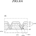
- FIGS. 8A and 8B are enlarged sectional views of an organic light emitting device according to still another exemplary embodiment.
- an organic light emitting device 400 includes, on a third insulation layer 460, a first electrode 441 that includes concave parts 441a and a first connection layer 441b that connects neighboring concave parts 441a, and an organic light emitting layer 442 and a second electrode 443 that are arranged in a shape following the morphology of the top surface of the first electrode 441.
- the shape of the concave parts 441a of the first electrode 441 is formed through the processes, such as photolithography, wet etching, and dry etching. In this case, the morphology of the concave parts 441a of the first electrode 441 can be adjusted when a heat treatment process performed at this time is adjusted.
- a separation distance G (gap) in the bottom 441ab or width of the bottom 441ab of each concave part 441a may be 0, and when the separation distance G (gap) is 0, an effective light emitting region may be increased so that light emitting efficiency is increased.
- the separation distance G (gap) in the bottom 441ab of the concave part 441a may be made to zero (0) by adjusting the heat treatment and etching time during the patterning process of the concave part 441a in the first electrode 441.
- the first electrode 441 may include a horizontal extension 447 to the outside of an inclined surface 441aa in the bottom 441ab of the concave part 441a. That is, a horizontal extension 447 of the first electrode may be formed along the bottom 441ab of the concave part 441a or between facing portions of the at least one inclined surface 441aa of the concave part 441 a.
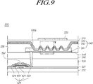
- FIG. 9 is a cross-sectional view of an organic light emitting device according to still another exemplary embodiment.
- an organic light emitting device 500 according to still another exemplary embodiment is described as a top emission type organic light emitting device in which a color filter 550 is located at the opposite side to the substrate 510, the organic light emitting device 500 may be a bottom emission type organic light emitting device in which a color filter 550 is located on the substrate 510 side.
- the top emission type organic light emitting device 500 has an advantage in life span and luminance because the aperture ratio is increased compared with the bottom emission type organic light emitting device.
- An organic light emitting device 500 according to still another exemplary embodiment is different from the bottom emission type organic light emitting device 100 of FIGS. 2 and 3A in that the organic light emitting device 500 includes a reflection plate 544 below the first electrode 541, includes an adhesive layer 570 between the second electrode 543 and the color filter 550, and the first electrode 541 includes a convex part 541c, and the other elements are substantially the same as the bottom emission type organic light emitting device 100. Thus, redundant descriptions will be omitted.
- the elements of the organic light emitting device 500 which are not illustrated in FIG. 9 , may be similar to the elements of the bottom emission type organic light emitting device 100 according to the above-described exemplary embodiments.
- a reflection plate 544 made of, for example, a conductive material may be disposed under the first electrode 541.
- the reflection plate 544 may reflect light emitted from the organic light emitting layer 542 to improve top emission efficiency.
- the reflection plate 544 may not be separately provided below the first electrode 541.
- the reflection plate 544 and the first electrode 541 may be connected to the source electrode 523 of the thin film transistor 520 through a contact hole formed in the third insulation layer 560.
- the first electrode 541 is connected to the source electrode 523 on the assumption that the thin film transistor 520 is an N-type thin film transistor.
- the reflection plate 544 and the first electrode 541 may be connected to the drain electrode 524.
- the first electrode 541 may be directly in contact with the organic light emitting layer 542, or may be in contact with the organic light emitting layer 542 with a conductive material being interposed therebetween so that the first electrode 541 can be electrically connected to the organic light emitting layer 542.
- FIG. 10 is an enlarged cross-sectional view for the region "Y" in FIG. 9 .
- the first electrode 541 includes convex parts 541c and a second connection part 541d that connects neighboring convex parts 541c.
- the first electrode 541 is flat in a portion where no convex part 541c is disposed.
- FIG. 10 although it is illustrated that a plurality of convex parts 541c are provided, for example, a single convex part 541c may be provided without being limited thereto.
- FIG. 11 is a partial perspective view illustrating the third insulation layer, the reflection plate, and the first electrode of FIG. 9 partially in cross section.
- the convex parts 541c have a positive-tapered shape that is narrowly inclined upward.
- the cross-sectional shape of the convex parts 541c may be a trapezoidal shape, but is not limited thereto.
- the convex parts 541c may have a truncated conical shape, but may be a polyhedron, such as a partially cut hexahedron or tetrahedron.
- the inclination ⁇ of the inclined surface 541ca of the convex part 541c means an angle formed by the inclined surface 541ca of the convex part 541c and the bottom surface of the first electrode 541, and the inclination ⁇ may be an acute angle.
- the inclination ⁇ of the inclined surface 541ca of the convex part 541c may be 15 to 70 degrees.
- the light extraction efficiency may be weak.
- the traveling angle of light, which starts to travel from an effective light emitting region may be 42 degrees or more. Consequently, the light may be confined again inside the organic light emitting diode 540 and the light emitting efficiency may not be increased.
- the separation distance G (gap) in the second connection portion 541d may be zero.
- the first electrode 541 may include an amorphous metal oxide, as described above.
- the organic light emitting layer 542 and the second electrode 543 is disposed in a shape that follows the morphology of the top surface of the first electrode 541. Accordingly, the organic light emitting layer 542 and the second electrode 543 have a convex morphology in the convex parts 541c of the first electrode 541. Consequently, the shape of the organic light emitting diode 540 may be implemented using the convex parts 541c of the first electrode 541.
- the thickness T3 of the organic light emitting layer 542, perpendicular to a surface of the first electrode 541, may be relatively thin in a region corresponding to the inclined surface 541ca of each convex part 541c, and may be thinner than the thickness T1 of the organic light emitting layer 542 on the top 541cb of the convex part 541c or the thickness T2 of the organic light emitting layer 542 on the second connection part 541 d of the first electrode 541.
- the thicknesses T1, T2, and T4 of the organic light emitting layer 542 deposited in a direction perpendicular to the substrate 510 are the same as each other.
- the thickness T3 of the organic light emitting layer 542 driving a current between the practical first and second electrodes 541 and 543 in the vertical direction on the inclined surface of the organic light emitting layer 542 becomes relatively thin.
- the thicknesses T1 and T2 of the organic light emitting layer 542 driving a current between the first electrode 541 and the second electrode 543 are relatively thick in the top 541 cb of the convex part 541 c and the second connection part 541 d.
- the thickness T3 of the organic light emitting layer 542, which is perpendicular to the first electrode 541 in the region corresponding to the inclined surface 541ca, is reduced as the inclination ⁇ of the inclined surface 541ca of the convex part 541c is increased.
- the thickness T3 of the organic light emitting layer 542, which is perpendicular to the first electrode 541 in the region corresponding to the inclined surface 541ca, and the inclination ⁇ of the inclined surface 541ca of the convex part 541c are determined according to Equation 1 described above.
- the thickness of the organic light emitting layer 542 in a region corresponding to the inclined surface 541ca of each convex part 541c may be relatively thinner than the part of the thickness of the organic light emitting layer 542 adjacent to the top 541 cb of the convex part 541c or the second connection part 541 d.
- the thickness of the organic light emitting layer 542 in a region corresponding to the inclined surface 541ca of each convex part 541c being relatively thin may result in an efficient light emitting region in which electric fields are locally concentrated.
- electric fields are locally concentrated in the efficient light emitting region, and a main current path is formed to generate the main light emission.
- T3 is a value of T1 reduced by 15%-50%, T2 reduced by 15%-50%, or T4 reduced by 15%-50%.
- T3 is T1 (or T2, or T4) reduced by less than 15%, light emission quantity is not enhanced significantly.
- T3 is T1 (or T2, or T4) reduced by more than 50%, light emission quantity may be significantly enhanced but the organic light emitting layer 542 is so thin that the life of the organic light emitting device 100 may be deteriorated.
- the organic light emitting layer 542 is made to have a thickness of T3 thinner than T1 or T2 or T4 by a modest amount (i.e., T1 or T2 or T4 reduced by 15%-50%) to achieve enhancement of light emission and life of the organic light emitting device at the same time.
- the light emission quantity per unit area of the organic light emitting layer 542 in the inclined surface 541ca between the convex part 541 c and the second connection part 541d of the first electrode 541 may be larger than the light emission quantity per unit area of the organic light emitting layer 542 in the top 541cb of the convex part 541c or the second connection part 541d.
- FIG. 12 is a view briefly illustrating an organic light emitting display device in a case where the organic light emitting device according to the exemplary embodiments is an organic light emitting diode display device.
- an organic light emitting diode display panel 600 includes: an organic light emitting display panel 610 in which a plurality of data lines DL and a plurality of gate lines GL are disposed, and a plurality of subpixels SP are disposed in a matrix type; a data driver 620 configured to drive the plurality of data lines by supplying a data voltage to the plurality of data lines; a gate driver 630 configured to sequentially drive the plurality of gate lines by sequentially supplying a scan signal to the plurality of gate lines; and a controller 640 configured to control the data driver 620 and the gate driver 630.
- FIG. 13 is a view briefly illustrating a lighting device in a case where the organic light emitting device according to the exemplary embodiments is a lighting device.
- a lighting device 700 includes a lighting unit 710, a controller 740 that controls the lighting unit 710, and the like.
- the lighting device 700 may separately include a driver like the organic light emitting display device 600, but is not limited thereto.
- the organic light emitting device is a lighting device 700, as described above, it may be an indoor or outdoor lighting device, a vehicular lighting device, or the like, or may be combined with another mechanical member to be applied to the above-described lighting devices.
- FIG. 13 illustrates the organic light emitting device according to exemplary embodiments as a lighting device 700.
- the organic light emitting device may be, for example, a light source.
- an organic light emitting diode and an organic light emitting device can improve external light extraction efficiency by applying a concave or convex structure to the first electrode.
- an organic light emitting diode and an organic light emitting device can improve an outward light emitting efficiency and reduce power consumption.
Landscapes
- Physics & Mathematics (AREA)
- Optics & Photonics (AREA)
- Engineering & Computer Science (AREA)
- Microelectronics & Electronic Packaging (AREA)
- Geometry (AREA)
- Electroluminescent Light Sources (AREA)
Abstract
Description
- This application claims priority from Korean Patent Application No.
10-2016-0182068 - The present disclosure relates to an organic light emitting diode and an organic light emitting device that emits light.
- An organic light emitting device has advantages in that by using self-light emitting Organic Light Emitting Diodes (OLEDs), a response speed is high, a light emitting efficiency is high, a luminance is high, and a viewing angle is wide.
- Light emitted from an organic light emitting layer of the organic light emitting device passes through various elements of the organic light emitting device, and is emitted from the organic light emitting device. However, some light, which is emitted from the organic light emitting layer, is confined inside the organic light emitting diode device, rather than being emitted from the organic light emitting device. Therefore, the light extraction efficiency of the organic light emitting device becomes an issue. A method of attaching a Micro Lens Array (MLA) to the outside of a substrate of the organic light emitting device has been used in order to improve the light extraction efficiency of the organic light emitting device.
- In this background, an object of the present disclosure is to provide an organic light emitting diode and an organic light emitting device that improve an outward light emitting efficiency and reduce power consumption.
- An exemplary embodiment may provide an organic light emitting diode that includes a first electrode including at least one curved part, an organic light emitting layer disposed on the first electrode, and a second electrode disposed on the organic light emitting layer. Further, the exemplary embodiment may provide an organic light emitting device including the organic light emitting diode. That is, the first electrode may include at least one concave part (e.g. an indentation) and/or at least one convex part (e.g. a protrusion). Thus, the first electrode may have a corrugated surface. 17
- The concave part may include a concave bottom. or The convex part may include a convex top. The concave part and/or the convex part may include one or more inclined side surfaces. In some embodiments, a first thickness of the organic light emitting layer adjacent to said one or more of the inclined side surfaces is thinner than a second thickness of the organic light emitting layer adjacent to the concave bottom or the convex top. The first thickness may be thinner than the second thickness by 15%-50% of the second thickness. An inclined side surface of the concave part of the first electrode may form an acute angle with a bottom surface of the concave part of the first electrode. An inclined side surface of the the convex part of the first electrode may form an acute angle with a top surface of the convex part of the first electrode. The acute angle may range from 15 degrees to 70 degrees. The organic light emitting layer may have a thickness that is thinnest on the inclined side surface of the first electrode. A first thickness of the organic light emitting layer on the inclined side surface of the first electrode may be thinner than a second thickness of the organic light emitting layer on the bottom surface of the concave part of the first electrode by 15%-50% of the second thickness. A first thickness of the organic light emitting layer on the inclined side surface of the first electrode may be thinner than a second thickness of the organic light emitting layer on the top surface of the convex part of the first electrode by 15%-50% of the second thickness. The organic light emitting layer and the second electrode may be arranged following a shape of a top surface of the first electrode. The first electrode may include an amorphous metal oxide. The amorphous metal oxide may include at least one selected from a group consisting of Indium Zinc Oxide (IZO), Zinc Tin Oxide (ZTO), SnO2 (tin oxide), ZnO (zinc oxide), In2O3 (indium oxide), Gallium Indium Tin Oxide (GITO), Indium Gallium Zinc Oxide (IGZO), Zinc Indium Tin Oxide (ZITO), Indium Gallium Oxide (IGO), Ga2O3 (gallium oxide), Aluminum Zinc Oxide (AZO), and Gallium Zinc Oxide (GZO). The first electrode may include the concave part together with another concave part and a connection part that is disposed between the concave part and said another concave part. The connection part may be flat. The organic light emitting device may further comprise a substrate; a thin film transistor on the substrate; and one or more insulation layers on the thin film transistor, the first electrode disposed on the one or more insulation layers and electrically connected to the thin film transistor through the one or more insulation layers. The organic light emitting device may further comprise a color filter disposed in or on the one or more insulation layers to overlap with at least a part of the organic light emitting layer. A concave bottom of the concave part may be in contact with the one or more insulation layers. A concave bottom of the concave part may be disposed over the one or more insulation layers with a gap therebetween. A concave bottom of the concave part may be flat. A concave bottom of the concave part may be pointy to form an angle with a surface of the one or more insulation layers. The concave part and/or the convex part may have a three-dimensionally tapered shape, i.e. a conical shape. The concave part and/or the convex part may have a cross-section of one of a circular shape, a hemispherical shape, a semi-ellipsoidal shape, a square shape, and a hexagonal shape. Here, cross-section may refer to a section parallel to the connection part, or parallel to a substrate on which the first electrode is formed.
- According to the present exemplary embodiment as described above, it is possible to provide an organic light emitting diode and an organic light emitting device that can improve an external light emitting efficiency and can reduce power consumption.
- The above and other objects, features, and advantages of the present disclosure will be more apparent from the following detailed description taken in conjunction with the accompanying drawings, in which:
-
FIG. 1 is a cross-sectional view of an organic light emitting diode according to one exemplary embodiment; -
FIG. 2 is a cross-sectional view of an organic light emitting device according to one exemplary embodiment; -
FIG. 3A is an enlarged cross-sectional view for the region "X" inFIG. 2 ; -
FIG. 3B illustrates a plan view of the first electrode ofFIG. 2 and an enlarged sectional view of the region "X" ofFIG. 2 , which corresponds to the planar structure of the first electrode; -
FIG. 4 is a partial perspective view illustrating the third insulation layer and the first electrode ofFIG. 2 in which an end surface is partially cut away; -
FIG. 5 is an enlarged cross-sectional view of a part of the region "X" inFIG. 2 , illustrating optical paths of light emitted from an organic light emitting layer; -
FIG. 6 is a view illustrating optical paths of light emitted from an organic light emitting device according to a comparative example; -
FIG. 7 is a cross-sectional view of an organic light emitting device including a thin film transistor according to another exemplary embodiment before a first electrode is formed in the organic light emitting device; -
FIGS. 8A and8B are enlarged sectional views of an organic light emitting device according to still another exemplary embodiment; -
FIG. 9 is a cross-sectional view of an organic light emitting device according to still another exemplary embodiment. -
FIG. 10 is an enlarged cross-sectional view for the region "Y" inFIG. 9 ; -
FIG. 11 is a partial perspective view illustrating the third insulation layer, the reflection plate, and the first electrode ofFIG. 9 in which an end surface is partially cut away; -
FIG. 12 is a view briefly illustrating an organic light emitting display device in a case where the organic light emitting device according to the exemplary embodiments is an organic light emitting diode display device; and -
FIG. 13 is a view briefly illustrating a lighting device in a case where the organic light emitting device according to the exemplary embodiments is a lighting device. - Hereinafter, some embodiments of the present disclosure will be described in detail with reference to the accompanying illustrative drawings. In designating elements of the drawings by reference numerals, the same elements will be designated by the same reference numerals although they are shown in different drawings. Further, in the following description of the present disclosure, a detailed description of known functions and configurations incorporated herein will be omitted when it may make the subject matter of the present disclosure rather unclear.
- In addition, terms, such as first, second, A, B, (a), (b) or the like may be used herein when describing components of the present disclosure. Each of these terminologies is not used to define an essence, order or sequence of a corresponding component but used merely to distinguish the corresponding component from other component(s). In the case that it is described that a certain structural element "is connected to", "is coupled to", or "is in contact with" another structural element, it should be interpreted that another structural element may "be connected to", "be coupled to", or "be in contact with" the structural elements as well as that the certain structural element is directly connected to or is in direct contact with another structural element.
-
FIG. 1 is a cross-sectional view of an organic light emitting diode according to one exemplary embodiment. Referring toFIG. 1 , an organiclight emitting diode 10 includes a first electrode 41 including a concave part or a convex part, an organiclight emitting layer 42 disposed on the first electrode 41, and asecond electrode 43 disposed on the organiclight emitting layer 42. Detailed descriptions of a structure and a shape of the organiclight emitting diode 10 will be made later with reference toFIGS. 3A ,3B , and10 . -
FIG. 2 is a cross-sectional view of an organic light emitting device according to one exemplary embodiment.FIG. 3A is an enlarged cross-sectional view for the region "X" inFIG. 2 .FIG. 3B illustrates a plan view of the first electrode ofFIG. 2 and an enlarged sectional view of the region "X" ofFIG. 2 , which corresponds to the planar structure of the first electrode. - Referring to
FIG. 2 , an organiclight emitting device 100 according to an exemplary embodiment may be any of various light emitting devices that include an organic light emitting diode or an organic electric element including two electrodes and an organic layer between the two electrodes. The organiclight emitting device 100 may be one of an organic light emitting display device that displays an image, a lighting device, and a light source. For example, when the organiclight emitting device 100 is an organic light emitting diode display device, it may be, but not exclusively, at least one of a bottom emission display device, a top emission display device, a dual emission display device, a flexible display device, and a tranparent display device. - When the organic
light emitting device 100 is a lighting device, it may be an indoor or outdoor lighting device, a vehicular lighting device, or the like, or may be combined with another mechanical member to be applied to the above-described lighting devices. For example, the vehicular lighting device may be, but not exclusively, at least one of a head lamp, a high beam lamp, a tail lamp, a brake lamp, a back light, a stop lamp, a fog lamp, a turn signal light, and an auxiliary lamp. When the organiclight emitting device 100 is a light source, it may be efficiently applied to, for example: a light source of a backlight of a Liquid Crystal Display (LCD), various lighting sensors, a printer, or a copying machine; a light source of a vehicle instrument; a light source of a signal lamp, a sign lamp, or a surface light emitting body; a decoration; various lights; or the like. - Hereinafter, descriptions will be made assuming that the organic
light emitting device 100 is an organic light emitting diode display device. However, without being limited thereto, the organiclight emitting device 100 may be a lighting device or a light source. - Referring to
FIGS. 2 and3A , the organiclight emitting device 100 is illustrated as including asubstrate 110, athin film transistor 120, acolor filter 150, athird insulation layer 160, and an organiclight emitting diode 140, but is not limited thereto. For example, the organiclight emitting device 100 according to an exemplary embodiment may be an organic light emitting device including an organiclight emitting diode 140 on thesubstrate 110, and may be an organic light emitting device including athird insulation layer 160 on thesubstrate 110, and an organiclight emitting diode 140 on the third insulation layer 160.As illustrated inFIGS. 2 and3A , thethird insulation layer 160 may be disposed under thefirst electrode 141 of the organiclight emitting diode 140, and may be a flat insulation layer. The organiclight emitting device 100 illustrated inFIGS. 2 and3A is a bottom emission type organic light emitting device. However, the organiclight emitting device 100 according to an exemplary embodiment may be a top emission type organic light emitting device. - On the
substrate 110, thethin film transistor 120 is disposed, which includes agate electrode 121, anactive layer 122, asource electrode 123, and adrain electrode 124. More specifically, thegate electrode 121 is disposed on thesubstrate 110, afirst insulation layer 131 for insulating thegate electrode 121 and theactive layer 122 is formed on thegate electrode 121 and thesubstrate 110, and theactive layer 122 is disposed on thefirst insulation layer 131. Further, anetch stopper 132 is disposed on theactive layer 122, and thesource electrode 123 and thedrain electrode 124 are disposed on theactive layer 122 and theetch stopper 132. Thesource electrode 123 and thedrain electrode 124 are electrically connected with theactive layer 122 in a manner of being in contact with theactive layer 122, and are disposed on a partial region of theetch stopper 132. In some embodiments, theetch stopper 132 may not be provided. - In this specification, among various thin film transistors, which may be included in the organic
light emitting device 100, only a driving thin film transistor is illustrated for the convenience of description. In addition, in this specification, descriptions will be made assuming that thethin film transistor 120 has a bottom gate structure or an inverted staggered structure in which thegate electrode 121 is located on the opposite side of thesource electrode 123 and thedrain electrode 124 with reference to theactive layer 122. However, in other embodiments athin film transistor 120 having a coplanar structure or a top gate structure may also be used, in which thegate electrode 121 is positioned at the same side as thesource electrode 123 and thedrain electrode 124 with reference to theactive layer 122. - A
second insulation layer 133 is disposed on thethin film transistor 120, and acolor filter 150 is disposed on thesecond insulation layer 133. - Although
FIG. 2 illustrates that thesecond insulation layer 133 flattens the top portion of thethin film transistor 120. However, thesecond insulation layer 133 may be disposed following the surface shapes of the elements positioned therebelow, rather than flattening the top portion of thethin film transistor 120. - The
color filter 150 is configured to convert the color of light emitted from the organiclight emitting layer 142, and may be one of, for example, a red color filter, a green color filter, and a blue color filter. Thecolor filter 150 is disposed on thesecond insulation layer 133 at a position corresponding to a light emitting region. Here, the light emitting region means a region where the organiclight emitting layer 142 emits light by thefirst electrode 141 and thesecond electrode 143. Further, the description "thecolor filter 150 is disposed at a position corresponding to the light emitting region" means that thecolor filter 150 is disposed to prevent blurring and ghost phenomena from occurring due to a mutual mixing of lights emitted from neighboring light emitting regions. For example, thecolor filter 150 is arranged to be superimposed on the light emitting region. More specifically, thecolor filter 150 may have a size that is smaller than the light emitting region. However, the disposed position and size of thecolor filter 150 may be determined by various factors, such as a distance between thecolor filter 150 and thefirst electrode 141 and a distance between thecolor filter 150 and thethird insulation layer 160 and a distance between a light emitting region and a non-light emitting region, in addition to the size and position of the light emitting region. - The
third insulation layer 160 is disposed on thecolor filter 150 and thesecond insulation layer 133. AlthoughFIG. 2 illustrates that thesecond insulation layer 133 is included in the organiclight emitting device 100, in other embodiments thethird insulation layer 160 may be directly disposed on thethin film transistor 120 without using thesecond insulation layer 133. AlthoughFIG. 2 illustrates that thecolor filter 150 is disposed on thesecond insulation layer 133, thecolor filter 150 may be disposed at any position between thethird insulation layer 160 and thesubstrate 110 without being limited thereto. - A
bank layer 136 and the organiclight emitting diode 140 including thefirst electrode 141, the organiclight emitting layer 142, and thesecond electrode 143 are disposed on thethird insulation layer 160. At this time, although not illustrated, an insulative second insulation layer (not illustrated), which has a refractive index similar to that of thefirst electrode 141, may be added between thethird insulation layer 160 and thefirst electrode 141 to block outgassing from thethird insulation layer 160 from spreading to the organiclight emitting diode 140. - Specifically, the
first electrode 141 is disposed on thethird insulation layer 160 to supply electrons or holes to the organiclight emitting layer 142. Thefirst electrode 141 may be a positive pole, a pixel electrode, or an anode in a normal organic light emitting diode (OLED), and may be a negative pole, a pixel electrode, or a cathode in an inverted OLED. - The
first electrode 141 may be connected to thesource electrode 123 of thethin film transistor 120 through contact holes formed in thethird insulation layer 160 and thesecond insulation layer 133. Herein, it has been described that thefirst electrode 141 is connected to thesource electrode 123 on the assumption that thethin film transistor 120 is an N-type thin film transistor. However, when thethin film transistor 120 is a P-type thin film transistor, thefirst electrode 141 may be connected to thedrain electrode 124. Thefirst electrode 141 may be directly in contact with the organiclight emitting layer 142, or may be in contact with the organiclight emitting layer 142 with a conductive material being interposed therebetween so that thefirst electrode 141 can be electrically connected to the organiclight emitting layer 142. Thefirst electrode 141 may be a single layer, but may be a multilayer including two or more layers. - Referring to
FIG. 3A , thefirst electrode 141 includesconcave parts 141a and afirst connection part 141b connecting neighboringconcave parts 141a. Thefirst electrode 141 is flat in a part where noconcave part 141 a is disposed. That is, thefirst connection part 141 b is flat or plane. Referring toFIG. 3A , although it is illustrated that a plurality ofconcave parts 141a are provided. However, for example, a singleconcave part 141a may be provided without being limited thereto.FIG. 4 is a partial perspective view illustrating the third insulation layer and the first electrode ofFIG. 2 partially in cross section. - Referring to
FIG. 3B andFIG. 4 , theconcave part 141a may have a shape inclined to be narrowed downward. Theconcave part 141a may include at least one inclined surface 141aa and a bottom 141ab. The bottom 141ab may be flat and/or parallel to thefirst connection part 141b. The bottom 141ab of theconcave part 141a may be surrounded by the inclined surface 141aa. The inclined surface 141aa may be located between the bottom 141ab and thefirst connection part 141b. Theconcave part 141a may be symmetric, e.g. with respect to a line perpendicular to thefirst connection part 141b. Theconcave part 141a may have a constant taper shape. For example, the cross-sectional shape of theconcave part 141a may be a trapezoidal shape, but is not limited thereto. Theconcave part 141 a may have a larger width on a level with thefirst connection part 141b than on a level with the bottom 141ab. The inclination θ of the inclined surface 141aa of theconcave part 141 a means an angle formed by theinclined surface 141 aa of theconcave part 141 a and a bottom surface of thefirst electrode 141. Here, the bottom surface of thefirst electrode 141 may refer to a surface of the first electrode that is in contact with an insulation layer, i.e. to a surface that is not in contact with the organiclight emitting layer 142. The inclination θ may be an acute angle. That is, the bottom surface of thefirst electrode 141 may be flat or plane, e.g. parallel to the surface of thefirst connection part 141b or to thesubstrate 110.FIG. 3B illustrates that the inclined surface 141aa of theconcave part 141a is linear in a cross section, andFIG. 4 illustrates that the inclined surface 141aa of theconcave part 141a is flat. However, the inclined surface 141aa of theconcave part 141a may be generally linear or planar, although it may include a non-linear or curved surface in a cross section. - The inclination θ of the inclined surface 141aa of the
concave part 141 a may be 15 to 70 degrees. When the inclination θ of the inclined surface 141aa of theconcave part 141 a has a small angle of less than 15 degrees, the light extraction efficiency may be weak. When the inclination θ of the inclined surface 141aa has a large angle of more than 70 degrees, the traveling angle of light, which starts to travel from an effective light emitting region, may be 42 degrees or more. Consequently, the light may be confined again inside the organiclight emitting diode 140 and the light emitting efficiency may not be increased. - Referring to
FIGS. 3A and3B , although it is illustrated that an interval is present in a case where a separation distance G (gap) at the bottom 141ab of theconcave part 141a or rather a width of the bottom 141ab is larger than 0, the separation distance G (gap), i.e. the smallest interval between two oppsite portions of the inclined surface 141aa of oneconcave part 141a or the width of the bottom 141ab of theconcave part 141a, may be zero (i.e., two facing portions of the inclined surfaces 141aa of theconcave part 141a may be adjacent to each other without a gap G, i.e. theconcave part 141a may have a triangular cross-section, rather than a trapezoidal one), as will be described later with reference toFIG. 8A . Also, although inFig. 3A and3B , it is illustrated that the bottom 141ab of theconcave part 141a is open, i.e. that thefirst electrode 141 exposes the organiclight emitting layer 142 at bottoms 141ab of theconcave parts 141a, material of thefirst electrode 141 may be present at the bottoms 141ab of theconcave parts 141 a. - As illustrated in
FIGS. 3B and4 , theconcave parts 141a may have a circular shape as a whole in a plan view, i.e. in a plane parallel to thesubstrate 110 or in a plane parallel to thefirst connection part 141 b or thebottoms 141 ab of the concave parts. However, without being limited thereto, theconcave parts 141a may have various shapes, such as a hemispherical shape, a semi-ellipsoidal shape, a square shape, and a hexagonal shape. The shape of theconcave parts 141 a of thefirst electrode 141 is formed through the processes, such as photolithography, wet etching, and dry etching. In this case, the morphology of theconcave parts 141a of thefirst electrode 141 can be adjusted when a heat treatment process performed at this time is adjusted. - In terms of material, the
first electrode 141 may include an amorphous metal oxide. For example, the amorphous metal oxide may include any one selected from a group consisting of Indium Zinc Oxide (IZO), Zinc Tin Oxide (ZTO), SnO2 (tin oxide), ZnO (zinc oxide), In2O3 (indium oxide), Gallium Indium Tin Oxide (GITO), Indium Gallium Zinc Oxide (IGZO), Zinc Indium Tin Oxide (ZITO), Indium Gallium Oxide (IGO), Ga2O3 (gallium oxide), Aluminum Zinc Oxide (AZO) and Gallium Zinc Oxide (GZO). - When the
first electrode 141 includes the amorphous metal oxide, it may be suitable for forming theconcave portion 141a of thefirst electrode 141 to the three-dimensionally constant taper shape through processes such as photolithography, wet etching, and dry etching. In terms of material-process relationship, it is possible to form theconcave portion 141a of thefirst electrode 141 to a three-dimensionally reverse taper shape if the material of thefirst electrode 141 is selected incorrectly. Abank layer 136 is disposed on thethird insulation layer 160 and thefirst electrode 141, and thebank layer 136 includes anopening 136a that exposes thefirst electrode 141. Thebank layer 136 serves to separate neighboring pixels (or sub-pixels) regions, and may be disposed between neighboring pixel (or sub-pixel) regions. Theconcave parts 141a and thefirst connection part 141b of thefirst electrode 141 are disposed to be superimposed on theopening 136a of thebank layer 136. - The organic
light emitting layer 142 is disposed on thefirst electrode 141, and thesecond electrode 143 is disposed on the organiclight emitting layer 142 to supply electrons or holes to the organiclight emitting layer 142. The organiclight emitting layer 142 is disposed in a tandem white structure in which a plurality of organic light emitting layers are stacked in order to emit white light. The organiclight emitting layer 142 may include a first organic light emitting layer that emits blue light and a second organic light emitting layer that is disposed on the first organic light emitting layer and emits light having a color that becomes white when mixed with blue. The second organic light emitting layer may be an organic light emitting layer that emits, for example, yellow green light. In the meantime, the organiclight emitting layer 142 may only include an organic light emitting layer that emits one of blue light, red light, and green light. In this case, thecolor filter 150 may not be included. Thesecond electrode 143 may be a negative pole, a common electrode, or a cathode in a normal organic light emitting diode (OLED), and may be a positive pole, a common electrode, or an anode in an inverted OLED. - The organic
light emitting layer 142 and thesecond electrode 143 are disposed in a shape that follows the morphology of the top surface of thefirst electrode 141. Accordingly, the organiclight emitting layer 142 and thesecond electrode 143 have a concave morphology in theconcave parts 141 a of thefirst electrode 141. Consequently, the shape of the organiclight emitting diode 140 may be implemented using theconcave parts 141 a of thefirst electrode 141. In other words, the organiclight emitting diode 140 may be configured with indentations corresponding to theconcave parts 141 a of thefirst electrode 141. - A thickness of the organic
light emitting layer 142 in a direction perpendicular to a surface of thefirst electrode 141 may be relatively thin in a region corresponding to the inclined surface 141aa of theconcave part 141a. Thus, a thickness T3 of the organic light emitting layer 142in a region corresponding to the inclined surface 141aa of theconcave part 141 a may be thinner than a thickness T2 of the organic light emitting layer 142in a region corresponding to the bottom 141ab of theconcave part 141a and/or a thickness T1 of the organiclight emitting layer 142 in a region corresponding to thefirst connection part 141b of thefirst electrode 141, i.e. T3 < T1, T2 (seeFig. 3B ). - For example, when the organic
light emitting layer 142 is formed through a vapor deposition process, the thicknesses T1, T2, and T4 of the organiclight emitting layer 142 deposited in a direction perpendicular to thesubstrate 110 are about the same. However, due to the characteristics of the vapor deposition process, the thickness T3 of the organiclight emitting layer 142 in vertical direction to the inclined surface of the organiclight emitting layer 142 driving a current between the first andsecond electrodes light emitting layer 142 in regions corresponding to the bottom 141ab of theconcave part 141a and to thefirst connection part 141b driving a current between thefirst electrode 141 and thesecond electrode 143 are relatively thick. - The thickness T3 of the organic
light emitting layer 142, which is perpendicular to thefirst electrode 141 in the region corresponding to the inclined surface 141aa of eachconcave part 141 a, is reduced as the inclination θ of the inclined surface 141aa of theconcave part 141a is increased. The thickness T3 of the organiclight emitting layer 142, which is perpendicular to thefirst electrode 141 in the region corresponding to the inclined surface 141aa of eachconcave part 141 a, and the inclination θ of the inclined surface 141aa of theconcave part 141a are determined according toEquation 1 as follows.
- As described above, the thickness of the organic
light emitting layer 142 in a region corresponding to the inclined surface 141aa of eachconcave part 141a may be relatively thinner than the part of the thickness of the organiclight emitting layer 142 adjacent to the bottom 141ab of theconcave part 141a or thefirst connection part 141b of thefirst electrode 141. - The thickness of the organic
light emitting layer 142 in a region corresponding to the inclined surface 141aa of eachconcave part 141 a being relatively thin may result in an efficient light emitting region in which electric fields are locally concentrated. When the organiclight emitting diode 140 is driven, electric fields are locally concentrated in the efficient light emitting region, and a main current path is formed to generate the main light emission. - In one embodiment, T3 is a value of T1 reduced by 15%-50%, T2 reduced by 15%-50%, or T4 reduced by 15%-50%. When T3 is T1 (or T2, or T4) reduced by less than 15%, light emission quantity is not enhanced significantly. On the other hand, when T3 is T1 (or T2, or T4) reduced by more than 50%, light emission quantity may be significantly enhanced but the organic
light emitting layer 142 is so thin that the life of the organiclight emitting device 100 may be deteriorated. Therefore, the organiclight emitting layer 142 is made to have a thickness of T3 thinner than T1 or T2 or T4 by a modest amount (i.e., 50% - 85% of T1 or T2 or T4, i.e. T1 or T2 or T4 reduced by 15%-50%) to achieve enhancement of light emission and life of the organic light emitting device at the same time. - In view of the light emission quantity of the organic
light emitting layer 142 depending on the thicknesses (T1, T2, T3, etc.) of the organiclight emitting layer 142, which is perpendicular to thefirst electrode 141, the light emission quantity per unit area of the organiclight emitting layer 142 in the inclined surface 141aa between the bottom 141ab of theconcave part 141a and thefirst connection part 141b of thefirst electrode 141 may be larger than the light emission quantity per unit area of the organiclight emitting layer 142 in the bottom 141 ab of theconcave part 141 a or thefirst connection part 141b. -
FIG. 5 is an enlarged cross-sectional view of a part of the region "X" inFIG. 2 , illustrating optical paths of light emitted from an organic light emitting layer. Referring toFIG. 5 , the light emitted from the organiclight emitting layer 142, which is confined by being totally reflected in thefirst electrode 141 and the organiclight emitting layer 142, is extracted to the outside by being re-reflected from thesecond electrode 143 positioned to correspond to the inclined surface 141aa by the concave structure of thefirst electrode 141, so that outward light emitting efficiency can be improved. -
FIG. 6 is a view illustrating optical paths of light emitted from an organic light emitting device according to a comparative example. Referring toFIG. 6 , the organiclight emitting device 100c according to the comparative example includes afirst insulation layer 131, asecond insulation layer 133, and athird insulation layer 160 on asubstrate 110. Unlike the organiclight emitting device 100 according to the exemplary embodiment illustrated inFIG. 3A , the organiclight emitting device 100c according to the comparative example includes, on athird insulation layer 160, an organiclight emitting diode 140c that includes a flatfirst electrode 141 c, an organiclight emitting layer 142c, and asecond electrode 143c. Approximately 80% of light emitted from the organiclight emitting layer 142c is confined inside the organiclight emitting device 100c, and only 20% of light is extracted to the outside. Therefore, there is a problem in that the optical efficiency of the organiclight emitting device 100c is very low. -
FIG. 7 is a cross-sectional view of an organic light emitting device including a thin film transistor according to another exemplary embodiment before a first electrode is formed in the organic light emitting device. Referring toFIG. 7 , in a manufacturing process of an organiclight emitting device 300 including a thin film transistor according to another exemplary embodiment, athin film transistor 320, which includes agate electrode 321, anactive layer 322, asource electrode 323, and adrain electrode 324, is formed on asubstrate 310. Agate insulating layer 331 may be located between thegate electrode 321 and theactive layer 322. Thereafter, a second insulation layer (not shown), acolor filter 350, and athird insulation layer 360 are formed on thethin film transistor 320 similarly to the description inFIG. 2 . When thethird insulation layer 360 is formed, as illustrated inFIG. 7 , only the second region corresponding to thethin film transistor 320 may be patterned so as to reduce the thickness of a firstelectrode contact hole 368 and the third insulatinglayer 360 in the third insulatinglayer 360, and the first region corresponding to thecolor filter 350 may not be patterned. Thus, the patterning process of thethird insulation layer 360 can be simplified. -
FIGS. 8A and8B are enlarged sectional views of an organic light emitting device according to still another exemplary embodiment. Referring toFIGS. 8A and8B , an organiclight emitting device 400 according to still another exemplary embodiment includes, on athird insulation layer 460, afirst electrode 441 that includesconcave parts 441a and afirst connection layer 441b that connects neighboringconcave parts 441a, and an organiclight emitting layer 442 and asecond electrode 443 that are arranged in a shape following the morphology of the top surface of thefirst electrode 441. As illustrated above, the shape of theconcave parts 441a of thefirst electrode 441 is formed through the processes, such as photolithography, wet etching, and dry etching. In this case, the morphology of theconcave parts 441a of thefirst electrode 441 can be adjusted when a heat treatment process performed at this time is adjusted. - Referring to
FIG. 8A , a separation distance G (gap) in the bottom 441ab or width of the bottom 441ab of eachconcave part 441a may be 0, and when the separation distance G (gap) is 0, an effective light emitting region may be increased so that light emitting efficiency is increased. The separation distance G (gap) in the bottom 441ab of theconcave part 441a may be made to zero (0) by adjusting the heat treatment and etching time during the patterning process of theconcave part 441a in thefirst electrode 441. Referring toFIG. 8B , when the separation distance G (gap) in the bottom 441ab of eachconcave part 441 a is larger than 0 and an interval is present, thefirst electrode 441 may include ahorizontal extension 447 to the outside of an inclined surface 441aa in the bottom 441ab of theconcave part 441a. That is, ahorizontal extension 447 of the first electrode may be formed along the bottom 441ab of theconcave part 441a or between facing portions of the at least one inclined surface 441aa of theconcave part 441 a. -
FIG. 9 is a cross-sectional view of an organic light emitting device according to still another exemplary embodiment. Referring toFIG. 9 , although an organiclight emitting device 500 according to still another exemplary embodiment is described as a top emission type organic light emitting device in which acolor filter 550 is located at the opposite side to thesubstrate 510, the organiclight emitting device 500 may be a bottom emission type organic light emitting device in which acolor filter 550 is located on thesubstrate 510 side. The top emission type organiclight emitting device 500 has an advantage in life span and luminance because the aperture ratio is increased compared with the bottom emission type organic light emitting device. - An organic
light emitting device 500 according to still another exemplary embodiment is different from the bottom emission type organiclight emitting device 100 ofFIGS. 2 and3A in that the organiclight emitting device 500 includes areflection plate 544 below thefirst electrode 541, includes anadhesive layer 570 between thesecond electrode 543 and thecolor filter 550, and thefirst electrode 541 includes aconvex part 541c, and the other elements are substantially the same as the bottom emission type organiclight emitting device 100. Thus, redundant descriptions will be omitted. The elements of the organiclight emitting device 500, which are not illustrated inFIG. 9 , may be similar to the elements of the bottom emission type organiclight emitting device 100 according to the above-described exemplary embodiments. - A
reflection plate 544 made of, for example, a conductive material may be disposed under thefirst electrode 541. Thereflection plate 544 may reflect light emitted from the organiclight emitting layer 542 to improve top emission efficiency. When thefirst electrode 541 itself functions as the reflection plate, thereflection plate 544 may not be separately provided below thefirst electrode 541. - The
reflection plate 544 and thefirst electrode 541 may be connected to thesource electrode 523 of thethin film transistor 520 through a contact hole formed in thethird insulation layer 560. Herein, it has been described that thefirst electrode 541 is connected to thesource electrode 523 on the assumption that thethin film transistor 520 is an N-type thin film transistor. However, when thethin film transistor 520 is a P-type thin film transistor, thereflection plate 544 and thefirst electrode 541 may be connected to thedrain electrode 524. Thefirst electrode 541 may be directly in contact with the organiclight emitting layer 542, or may be in contact with the organiclight emitting layer 542 with a conductive material being interposed therebetween so that thefirst electrode 541 can be electrically connected to the organiclight emitting layer 542. -
FIG. 10 is an enlarged cross-sectional view for the region "Y" inFIG. 9 . Referring toFIG. 10 , thefirst electrode 541 includesconvex parts 541c and asecond connection part 541d that connects neighboringconvex parts 541c. Thefirst electrode 541 is flat in a portion where noconvex part 541c is disposed. Referring toFIG. 10 , although it is illustrated that a plurality ofconvex parts 541c are provided, for example, a singleconvex part 541c may be provided without being limited thereto. -
FIG. 11 is a partial perspective view illustrating the third insulation layer, the reflection plate, and the first electrode ofFIG. 9 partially in cross section. Theconvex parts 541c have a positive-tapered shape that is narrowly inclined upward. For example, the cross-sectional shape of theconvex parts 541c may be a trapezoidal shape, but is not limited thereto. Theconvex parts 541c may have a truncated conical shape, but may be a polyhedron, such as a partially cut hexahedron or tetrahedron. - The inclination θ of the inclined surface 541ca of the
convex part 541c means an angle formed by the inclined surface 541ca of theconvex part 541c and the bottom surface of thefirst electrode 541, and the inclination θ may be an acute angle. - The inclination θ of the inclined surface 541ca of the
convex part 541c may be 15 to 70 degrees. When the inclination θ of the inclined surface 541ca of theconvex part 541c has a small angle of less than 15 degrees, the light extraction efficiency may be weak. When the inclination θ of the inclined surface 541ca is a large angle of more than 70 degrees, the traveling angle of light, which starts to travel from an effective light emitting region, may be 42 degrees or more. Consequently, the light may be confined again inside the organiclight emitting diode 540 and the light emitting efficiency may not be increased. - Although it is illustrated that an interval is present in a case where the separation distance G (gap) in the
second connection portion 541d, or rather a width of thesecond connection portion 541d between neighboringconvex parts 541 c, is larger than 0, the separation distance G (gap between neighboringconvex parts 541c) may be zero. In terms of material, thefirst electrode 541 may include an amorphous metal oxide, as described above. - The organic
light emitting layer 542 and thesecond electrode 543 is disposed in a shape that follows the morphology of the top surface of thefirst electrode 541. Accordingly, the organiclight emitting layer 542 and thesecond electrode 543 have a convex morphology in theconvex parts 541c of thefirst electrode 541. Consequently, the shape of the organiclight emitting diode 540 may be implemented using theconvex parts 541c of thefirst electrode 541. - Referring to
FIG. 10 , the thickness T3 of the organiclight emitting layer 542, perpendicular to a surface of thefirst electrode 541, may be relatively thin in a region corresponding to the inclined surface 541ca of eachconvex part 541c, and may be thinner than the thickness T1 of the organiclight emitting layer 542 on the top 541cb of theconvex part 541c or the thickness T2 of the organiclight emitting layer 542 on thesecond connection part 541 d of thefirst electrode 541. - For example, when the organic
light emitting layer 542 is formed through a vapor deposition process, the thicknesses T1, T2, and T4 of the organiclight emitting layer 542 deposited in a direction perpendicular to thesubstrate 510 are the same as each other. However, due to the characteristics of the vapor deposition process, the thickness T3 of the organiclight emitting layer 542 driving a current between the practical first andsecond electrodes light emitting layer 542 becomes relatively thin. The thicknesses T1 and T2 of the organiclight emitting layer 542 driving a current between thefirst electrode 541 and thesecond electrode 543 are relatively thick in the top 541 cb of theconvex part 541 c and thesecond connection part 541 d. - The thickness T3 of the organic
light emitting layer 542, which is perpendicular to thefirst electrode 541 in the region corresponding to the inclined surface 541ca, is reduced as the inclination θ of the inclined surface 541ca of theconvex part 541c is increased. The thickness T3 of the organiclight emitting layer 542, which is perpendicular to thefirst electrode 541 in the region corresponding to the inclined surface 541ca, and the inclination θ of the inclined surface 541ca of theconvex part 541c are determined according toEquation 1 described above. - As described above, the thickness of the organic
light emitting layer 542 in a region corresponding to the inclined surface 541ca of eachconvex part 541c may be relatively thinner than the part of the thickness of the organiclight emitting layer 542 adjacent to the top 541 cb of theconvex part 541c or thesecond connection part 541 d. - The thickness of the organic
light emitting layer 542 in a region corresponding to the inclined surface 541ca of eachconvex part 541c being relatively thin may result in an efficient light emitting region in which electric fields are locally concentrated. When the organiclight emitting diode 540 is driven, electric fields are locally concentrated in the efficient light emitting region, and a main current path is formed to generate the main light emission. - In one embodiment, T3 is a value of T1 reduced by 15%-50%, T2 reduced by 15%-50%, or T4 reduced by 15%-50%. When T3 is T1 (or T2, or T4) reduced by less than 15%, light emission quantity is not enhanced significantly. On the other hand, when T3 is T1 (or T2, or T4) reduced by more than 50%, light emission quantity may be significantly enhanced but the organic
light emitting layer 542 is so thin that the life of the organiclight emitting device 100 may be deteriorated. Therefore, the organiclight emitting layer 542 is made to have a thickness of T3 thinner than T1 or T2 or T4 by a modest amount (i.e., T1 or T2 or T4 reduced by 15%-50%) to achieve enhancement of light emission and life of the organic light emitting device at the same time. - In view of the light emission quantity of the organic
light emitting layer 542 depending on the thicknesses (T1, T2, T3, etc.) of the organiclight emitting layer 542, which is perpendicular to thefirst electrode 541, the light emission quantity per unit area of the organiclight emitting layer 542 in the inclined surface 541ca between theconvex part 541 c and thesecond connection part 541d of thefirst electrode 541 may be larger than the light emission quantity per unit area of the organiclight emitting layer 542 in the top 541cb of theconvex part 541c or thesecond connection part 541d. -
FIG. 12 is a view briefly illustrating an organic light emitting display device in a case where the organic light emitting device according to the exemplary embodiments is an organic light emitting diode display device. - Referring to
FIG. 12 , an organic light emittingdiode display panel 600 according to the exemplary embodiments includes: an organic light emittingdisplay panel 610 in which a plurality of data lines DL and a plurality of gate lines GL are disposed, and a plurality of subpixels SP are disposed in a matrix type; adata driver 620 configured to drive the plurality of data lines by supplying a data voltage to the plurality of data lines; agate driver 630 configured to sequentially drive the plurality of gate lines by sequentially supplying a scan signal to the plurality of gate lines; and acontroller 640 configured to control thedata driver 620 and thegate driver 630. -
FIG. 13 is a view briefly illustrating a lighting device in a case where the organic light emitting device according to the exemplary embodiments is a lighting device. - Referring to
FIG. 13 , alighting device 700 according to exemplary embodiments includes alighting unit 710, acontroller 740 that controls thelighting unit 710, and the like. Thelighting device 700 may separately include a driver like the organic light emittingdisplay device 600, but is not limited thereto. - In the case where the organic light emitting device is a
lighting device 700, as described above, it may be an indoor or outdoor lighting device, a vehicular lighting device, or the like, or may be combined with another mechanical member to be applied to the above-described lighting devices.FIG. 13 illustrates the organic light emitting device according to exemplary embodiments as alighting device 700. However, without being limited thereto, the organic light emitting device may be, for example, a light source. - According to the above-described exemplary embodiments, an organic light emitting diode and an organic light emitting device can improve external light extraction efficiency by applying a concave or convex structure to the first electrode.
- According to the above-described exemplary embodiments, an organic light emitting diode and an organic light emitting device can improve an outward light emitting efficiency and reduce power consumption.
- According to the above-described exemplary embodiments, it is possible to increase the lifetime of an organic light emitting diode and an organic light emitting device.
- The above description and the accompanying drawings provide an example of the technical idea of the present disclosure for illustrative purposes only. Those having ordinary knowledge in the technical field, to which the present disclosure pertains, will appreciate that various modifications and changes in form, such as combination, separation, substitution, and change of a configuration, are possible without departing from the essential features of the present disclosure. Therefore, the embodiments disclosed in the present disclosure are intended to illustrate the scope of the technical idea of the present disclosure, and the scope of the present disclosure is not limited by the embodiment. The scope of the present disclosure shall be construed on the basis of the accompanying claims in such a manner that all of the technical ideas included within the scope equivalent to the claims belong to the present disclosure.
Claims (15)
- An organic light emitting device comprising:a first electrode (141, 441, 541) having a plurality of curved parts (141a, 441a, 541d) and a connection part (141b, 441b, 541d) between the curved parts (141a, 441a, 541d), the curved parts including concave parts (141a, 441a) and/or convex parts (541c);an organic light emitting layer (142,442,542) disposed on the first electrode (141, 441, 541); anda second electrode (143, 443, 543) disposed on the organic light emitting layer (142, 442, 542).
- The organic light emitting device of claim 1, wherein the curved parts (141a, 441a, 541c) include one or more inclined side surfaces (141aa, 441aa, 541ca), respectively.
- The organic light emitting device of claim 2, wherein a first thickness (T3) of the organic light emitting layer (142,442,542) on the inclined side surfaces (141aa, 441aa, 541ca) is thinner than a second thickness (T1, T2) of the organic light emitting layer (142, 442, 542) on the connection part (141b, 441b, 541d).
- The organic light emitting device of claim 3, wherein the first thickness (T3) is about 50% to 85% of the second thickness (T1, T2).
- The organic light emitting device according to any one of the preceding claims 2 to 4, wherein the inclined side surface (141aa, 441aa, 541ca) forms an acute angle with a bottom surface of the first electrode (141, 441, 541) and/or with a substrate (110, 510) on which the first electrode (141, 441, 541) is formed, and ranges preferably from 15 degrees to 70 degrees.
- The organic light emitting device according to any one of the preceding claims 2 to 6, wherein an angle between the inclined side surface (141 aa, 441 aa, 541 ca) and the connection part (141b, 441b, 541d) is obtuse, and ranges preferably from 165 degrees to 110 degrees.
- The organic light emitting device according to any one of the preceding claims, wherein the organic light emitting layer (142,442,542) and/or the second electrode (143, 443, 543) have curved parts corresponding to that of the first electrode (141, 441, 541).
- The organic light emitting device according to any one of the preceding claims, wherein the connection part (141b, 441b, 541d) is flat and/or has a surface parallel to a substrate (110, 510) on which the first electrode (141, 441, 541) is formed.
- The organic light emitting device according to any one of the preceding claims, wherein the concave part (141 a, 441 a) or the convex part (541c) has a tapered or conical or pyramidal shape.
- The organic light emitting device according to any one of the preceding claims, wherein the concave part (141a, 441a) or the convex part (541c) has a cross-section of one of a circular shape, a hemispherical shape, a semi-ellipsoidal shape, a square shape, and a hexagonal shape.
- The organic light emitting device according to any one of the preceding claims, wherein a distance between adjacent curved parts (141a, 441a, 541c) and/or a width of the connection part between adjacent curved parts (141 a, 441 a, 541 c) is equal to or larger than 0.
- The organic light emitting device according to any one of the preceding claims, wherein the concave part includes a bottom (141ab, 441ab) surrounded by the inclined surface (141aa, 441aa) having a width equal to or larger than 0 or wherein the convex part (541c) includes a top (541cb) surrounded by the inclined surface (541ca) having a width equal to or larger than 0.
- The organic light emitting device according to any one of the preceding claims, further comprising:a substrate (110, 510);a thin film transistor (120, 520) on the substrate (110, 510); andone or more insulation layers (131, 133, 160; 460; 531, 533, 560) on the thin film transistor (120,520), the first electrode (141, 441, 541) disposed on the one or more insulation layers (131,133, 160; 460; 531, 533, 560) and electrically connected to the thin film transistor (120, 520) through the one or more insulation layers (131,133,160; 460; 531, 533, 560).
- The organic light emitting device of claim 13, further comprising a color filter (150, 550) overlapping with at least a part of the organic light emitting layer(142, 442, 542).
- A display panel (600) or a lighting device (700) including the organic light emitting device according to any one of the preceding claims.
Applications Claiming Priority (1)
| Application Number | Priority Date | Filing Date | Title |
|---|---|---|---|
| KR20160182068 | 2016-12-29 |
Publications (2)
| Publication Number | Publication Date |
|---|---|
| EP3343664A1 true EP3343664A1 (en) | 2018-07-04 |
| EP3343664B1 EP3343664B1 (en) | 2023-07-05 |
Family
ID=60856932
Family Applications (1)
| Application Number | Title | Priority Date | Filing Date |
|---|---|---|---|
| EP17211029.8A Active EP3343664B1 (en) | 2016-12-29 | 2017-12-29 | Organic light emitting device |
Country Status (4)
| Country | Link |
|---|---|
| US (3) | US10181574B2 (en) |
| EP (1) | EP3343664B1 (en) |
| KR (1) | KR102459044B1 (en) |
| CN (1) | CN108258140B (en) |
Cited By (1)
| Publication number | Priority date | Publication date | Assignee | Title |
|---|---|---|---|---|
| CN108987443A (en) * | 2018-07-05 | 2018-12-11 | 昆山国显光电有限公司 | Display panel and its manufacturing method and display terminal |
Families Citing this family (28)
| Publication number | Priority date | Publication date | Assignee | Title |
|---|---|---|---|---|
| CN111613651B (en) * | 2017-02-27 | 2024-06-07 | 乐金显示有限公司 | Organic light emitting device |
| US10418583B2 (en) | 2017-02-27 | 2019-09-17 | Lg Display Co., Ltd. | Organic light emitting device |
| JP7057147B2 (en) | 2018-01-31 | 2022-04-19 | ソニーセミコンダクタソリューションズ株式会社 | Light emitting element and display device |
| KR102582649B1 (en) * | 2018-02-12 | 2023-09-25 | 삼성디스플레이 주식회사 | Display device |
| CN109979983B (en) * | 2018-06-22 | 2021-05-28 | 友达光电股份有限公司 | Organic Light Emitting Diode Display Device |
| KR102622792B1 (en) * | 2018-08-30 | 2024-01-08 | 엘지디스플레이 주식회사 | Light emitting display device |
| CN208622729U (en) * | 2018-09-14 | 2019-03-19 | 京东方科技集团股份有限公司 | A kind of OLED display panel and display device |
| EP3884532B8 (en) | 2018-11-20 | 2026-01-14 | BOE Technology Group Co., Ltd. | Pixel structure, display apparatus, and method of fabricating pixel structure |
| KR102075741B1 (en) | 2018-12-17 | 2020-02-10 | 엘지디스플레이 주식회사 | Display panel |
| KR102075728B1 (en) | 2018-12-17 | 2020-02-10 | 엘지디스플레이 주식회사 | Display panel |
| CN111969121B (en) * | 2019-05-20 | 2024-06-25 | 乐金显示有限公司 | Light-emitting display device |
| CN110299389B (en) * | 2019-06-26 | 2021-06-04 | 合肥视涯技术有限公司 | Organic light emitting display device |
| KR102818425B1 (en) * | 2019-08-30 | 2025-06-10 | 엘지디스플레이 주식회사 | Light emitting display apparatus |
| KR102698613B1 (en) | 2019-09-20 | 2024-08-27 | 엘지디스플레이 주식회사 | Organic light emitting pannel and including organic light emitting display |
| US12342674B2 (en) * | 2019-11-14 | 2025-06-24 | Sharp Kabushiki Kaisha | Light-emitting element and display device |
| CN110910829B (en) * | 2019-11-26 | 2021-07-06 | 深圳市华星光电半导体显示技术有限公司 | OLED pixel structure and OLED display panel |
| US11765924B2 (en) | 2019-12-19 | 2023-09-19 | Lg Display Co., Ltd. | Light emitting display panel and light emitting display apparatus including the same |
| CN111900267B (en) * | 2020-08-11 | 2024-04-16 | 京东方科技集团股份有限公司 | Array substrate and display device |
| KR102830939B1 (en) * | 2020-12-29 | 2025-07-04 | 엘지디스플레이 주식회사 | Display device |
| KR102839630B1 (en) * | 2020-12-30 | 2025-07-28 | 엘지디스플레이 주식회사 | Display device |
| JP7734468B2 (en) * | 2021-03-11 | 2025-09-05 | パナソニックオートモーティブシステムズ株式会社 | Transparent display device |
| KR102898665B1 (en) * | 2021-11-16 | 2025-12-09 | 엘지디스플레이 주식회사 | Organic light emitting display apparatus |
| EP4646081A1 (en) * | 2022-12-30 | 2025-11-05 | Yas Co., Ltd. | Organic light-emitting display device |
| WO2024144091A1 (en) * | 2022-12-30 | 2024-07-04 | 주식회사 야스 | Organic light-emitting display device |
| KR20250132935A (en) * | 2024-02-29 | 2025-09-05 | 엘지디스플레이 주식회사 | Display device |
| CN118301982A (en) * | 2024-05-14 | 2024-07-05 | 京东方科技集团股份有限公司 | Display substrate, manufacturing method thereof, and display device |
| CN121751895A (en) * | 2024-09-27 | 2026-03-27 | 合肥京东方卓印科技有限公司 | Display substrate and display device |
| US20260107659A1 (en) * | 2024-10-16 | 2026-04-16 | Samsung Display Co., Ltd. | Display device and electronic device including the same |
Citations (4)
| Publication number | Priority date | Publication date | Assignee | Title |
|---|---|---|---|---|
| US20080024402A1 (en) * | 2004-04-30 | 2008-01-31 | Ryuji Nishikawa | Light-Emitting Display |
| US20100176717A1 (en) * | 2009-01-12 | 2010-07-15 | Samsung Mobile Display Co., Ltd. | Organic light emitting display device |
| EP2637480A1 (en) * | 2010-11-02 | 2013-09-11 | Oji Holdings Corporation | Organic light emitting diode, method for manufacturing same, image display device, and illuminating device |
| US20150097191A1 (en) * | 2013-10-07 | 2015-04-09 | Au Optronics Corporation | Pixel structure |
Family Cites Families (22)
| Publication number | Priority date | Publication date | Assignee | Title |
|---|---|---|---|---|
| US4774435A (en) | 1987-12-22 | 1988-09-27 | Gte Laboratories Incorporated | Thin film electroluminescent device |
| JP4294745B2 (en) | 1997-09-26 | 2009-07-15 | 株式会社半導体エネルギー研究所 | Method for manufacturing photoelectric conversion device |
| EP1248121A1 (en) * | 2000-10-12 | 2002-10-09 | Sanyo Electric Co., Ltd. | Method for forming color filter, method for forming light emitting element layer, method for manufacturing color display device comprising them, or color display device |
| US7038373B2 (en) * | 2002-07-16 | 2006-05-02 | Eastman Kodak Company | Organic light emitting diode display |
| JP2004063559A (en) * | 2002-07-25 | 2004-02-26 | Renesas Technology Corp | Semiconductor device |
| KR100908234B1 (en) * | 2003-02-13 | 2009-07-20 | 삼성모바일디스플레이주식회사 | EL display device and manufacturing method thereof |
| KR101326135B1 (en) * | 2006-11-27 | 2013-11-07 | 삼성디스플레이 주식회사 | Organic light emitting display and manufacturing method thereof |
| US20080237764A1 (en) * | 2007-03-30 | 2008-10-02 | Fujifilm Corporation | Semiconductor element and method for manufacturing the same |
| EP2245669A4 (en) * | 2008-01-31 | 2015-05-06 | Univ Northwestern | INORGANIC THIN FILM TRANSISTORS WITH HIGH MOBILITY AND TREATED BY A SOLUTION |
| US8629842B2 (en) * | 2008-07-11 | 2014-01-14 | Samsung Display Co., Ltd. | Organic light emitting display device |
| JP2011076774A (en) | 2009-09-29 | 2011-04-14 | Sony Corp | Light emitting device and display device |
| JP5827858B2 (en) | 2011-09-29 | 2015-12-02 | 株式会社半導体エネルギー研究所 | Light emitting device |
| JP6216540B2 (en) * | 2012-05-30 | 2017-10-18 | ローム株式会社 | ORGANIC EL LIGHT EMITTING DEVICE, ITS MANUFACTURING METHOD, AND LAMINATED COLOR FILTER |
| WO2013190813A1 (en) * | 2012-06-21 | 2013-12-27 | パナソニック株式会社 | Organic el display device and method for manufacturing same |
| CN103824875B (en) | 2013-12-10 | 2015-07-08 | 京东方科技集团股份有限公司 | OLED display panel, manufacturing method thereof and display device |
| JP2015122248A (en) * | 2013-12-25 | 2015-07-02 | 株式会社ジャパンディスプレイ | Organic EL display device |
| KR102230006B1 (en) * | 2014-03-18 | 2021-03-19 | 삼성디스플레이 주식회사 | Organic light emitting diode display |
| KR102178863B1 (en) | 2014-06-27 | 2020-11-13 | 엘지디스플레이 주식회사 | White organic light emitting display device |
| JP2016115747A (en) * | 2014-12-12 | 2016-06-23 | 株式会社Joled | Display device, manufacturing method of the same, and electronic apparatus |
| CN105161632A (en) * | 2015-08-03 | 2015-12-16 | 深圳市华星光电技术有限公司 | Organic electroluminescent device structure and preparation method thereof |
| KR101805552B1 (en) * | 2015-08-31 | 2017-12-08 | 엘지디스플레이 주식회사 | Organic Light Emitting Diode Display Device |
| KR101808715B1 (en) * | 2015-09-23 | 2017-12-14 | 엘지디스플레이 주식회사 | Organic light emitting display device |
-
2017
- 2017-05-11 US US15/593,029 patent/US10181574B2/en active Active
- 2017-09-29 KR KR1020170127126A patent/KR102459044B1/en active Active
- 2017-12-27 CN CN201711445224.3A patent/CN108258140B/en active Active
- 2017-12-29 EP EP17211029.8A patent/EP3343664B1/en active Active
-
2018
- 2018-05-11 US US15/976,975 patent/US10355234B2/en active Active
- 2018-12-06 US US16/212,459 patent/US10622578B2/en active Active
Patent Citations (4)
| Publication number | Priority date | Publication date | Assignee | Title |
|---|---|---|---|---|
| US20080024402A1 (en) * | 2004-04-30 | 2008-01-31 | Ryuji Nishikawa | Light-Emitting Display |
| US20100176717A1 (en) * | 2009-01-12 | 2010-07-15 | Samsung Mobile Display Co., Ltd. | Organic light emitting display device |
| EP2637480A1 (en) * | 2010-11-02 | 2013-09-11 | Oji Holdings Corporation | Organic light emitting diode, method for manufacturing same, image display device, and illuminating device |
| US20150097191A1 (en) * | 2013-10-07 | 2015-04-09 | Au Optronics Corporation | Pixel structure |
Cited By (2)
| Publication number | Priority date | Publication date | Assignee | Title |
|---|---|---|---|---|
| CN108987443A (en) * | 2018-07-05 | 2018-12-11 | 昆山国显光电有限公司 | Display panel and its manufacturing method and display terminal |
| CN108987443B (en) * | 2018-07-05 | 2021-06-11 | 昆山国显光电有限公司 | Display panel, manufacturing method thereof and display terminal |
Also Published As
| Publication number | Publication date |
|---|---|
| KR20180078128A (en) | 2018-07-09 |
| US10355234B2 (en) | 2019-07-16 |
| EP3343664B1 (en) | 2023-07-05 |
| CN108258140A (en) | 2018-07-06 |
| CN108258140B (en) | 2020-05-26 |
| US10181574B2 (en) | 2019-01-15 |
| US20180261794A1 (en) | 2018-09-13 |
| KR102459044B1 (en) | 2022-10-26 |
| US20180190932A1 (en) | 2018-07-05 |
| US10622578B2 (en) | 2020-04-14 |
| US20190109294A1 (en) | 2019-04-11 |
Similar Documents
| Publication | Publication Date | Title |
|---|---|---|
| US10622578B2 (en) | Organic light emitting device | |
| US10957871B2 (en) | Organic light emitting device | |
| US10319796B2 (en) | Organic light emitting display device | |
| JP5167723B2 (en) | Light emitting device | |
| CN106486525B (en) | Organic light emitting diode display device | |
| US20200020755A1 (en) | Organic light emitting diode display device and organic light emitting diode thereof | |
| CN109728183B (en) | Organic Light Emitting Diode Display Devices | |
| KR20150039487A (en) | Display device | |
| CN111613651B (en) | Organic light emitting device | |
| US20190067642A1 (en) | Electroluminescent Display Device | |
| CN108258134B (en) | Top-emission organic light emitting diode display device | |
| EP4099418A1 (en) | Organic light emitting device | |
| CN106098725B (en) | Organic light emitting display device | |
| KR101802778B1 (en) | Organic light emitting display device | |
| KR20190063964A (en) | Electroluminescent Display Device | |
| EP3343659A1 (en) | Top emission type organic light emitting diode display device | |
| KR20210097087A (en) | Organic light emitting display device | |
| KR20100064187A (en) | Display device and method for fabricating the same |
Legal Events
| Date | Code | Title | Description |
|---|---|---|---|
| PUAI | Public reference made under article 153(3) epc to a published international application that has entered the european phase |
Free format text: ORIGINAL CODE: 0009012 |
|
| STAA | Information on the status of an ep patent application or granted ep patent |
Free format text: STATUS: REQUEST FOR EXAMINATION WAS MADE |
|
| 17P | Request for examination filed |
Effective date: 20171229 |
|
| AK | Designated contracting states |
Kind code of ref document: A1 Designated state(s): AL AT BE BG CH CY CZ DE DK EE ES FI FR GB GR HR HU IE IS IT LI LT LU LV MC MK MT NL NO PL PT RO RS SE SI SK SM TR |
|
| AX | Request for extension of the european patent |
Extension state: BA ME |
|
| RBV | Designated contracting states (corrected) |
Designated state(s): AL AT BE BG CH CY CZ DE DK EE ES FI FR GB GR HR HU IE IS IT LI LT LU LV MC MK MT NL NO PL PT RO RS SE SI SK SM TR |
|
| STAA | Information on the status of an ep patent application or granted ep patent |
Free format text: STATUS: EXAMINATION IS IN PROGRESS |
|
| 17Q | First examination report despatched |
Effective date: 20201105 |
|
| REG | Reference to a national code |
Ref country code: DE Ref legal event code: R079 Free format text: PREVIOUS MAIN CLASS: H01L0051520000 Ipc: H10K0050813000 Ref country code: DE Ref legal event code: R079 Ref document number: 602017070890 Country of ref document: DE Free format text: PREVIOUS MAIN CLASS: H01L0051520000 Ipc: H10K0050813000 |
|
| GRAP | Despatch of communication of intention to grant a patent |
Free format text: ORIGINAL CODE: EPIDOSNIGR1 |
|
| STAA | Information on the status of an ep patent application or granted ep patent |
Free format text: STATUS: GRANT OF PATENT IS INTENDED |
|
| RIC1 | Information provided on ipc code assigned before grant |
Ipc: H10K 50/856 20230101ALN20230116BHEP Ipc: H10K 50/813 20230101AFI20230116BHEP |
|
| RIC1 | Information provided on ipc code assigned before grant |
Ipc: H10K 50/856 20230101ALN20230125BHEP Ipc: H10K 50/813 20230101AFI20230125BHEP |
|
| INTG | Intention to grant announced |
Effective date: 20230215 |
|
| GRAS | Grant fee paid |
Free format text: ORIGINAL CODE: EPIDOSNIGR3 |
|
| GRAA | (expected) grant |
Free format text: ORIGINAL CODE: 0009210 |
|
| STAA | Information on the status of an ep patent application or granted ep patent |
Free format text: STATUS: THE PATENT HAS BEEN GRANTED |
|
| AK | Designated contracting states |
Kind code of ref document: B1 Designated state(s): AL AT BE BG CH CY CZ DE DK EE ES FI FR GB GR HR HU IE IS IT LI LT LU LV MC MK MT NL NO PL PT RO RS SE SI SK SM TR |
|
| REG | Reference to a national code |
Ref country code: CH Ref legal event code: EP |
|
| REG | Reference to a national code |
Ref country code: AT Ref legal event code: REF Ref document number: 1586035 Country of ref document: AT Kind code of ref document: T Effective date: 20230715 |
|
| REG | Reference to a national code |
Ref country code: DE Ref legal event code: R096 Ref document number: 602017070890 Country of ref document: DE |
|
| REG | Reference to a national code |
Ref country code: IE Ref legal event code: FG4D |
|
| REG | Reference to a national code |
Ref country code: LT Ref legal event code: MG9D |
|
| REG | Reference to a national code |
Ref country code: NL Ref legal event code: MP Effective date: 20230705 |
|
| REG | Reference to a national code |
Ref country code: AT Ref legal event code: MK05 Ref document number: 1586035 Country of ref document: AT Kind code of ref document: T Effective date: 20230705 |
|
| PG25 | Lapsed in a contracting state [announced via postgrant information from national office to epo] |
Ref country code: NL Free format text: LAPSE BECAUSE OF FAILURE TO SUBMIT A TRANSLATION OF THE DESCRIPTION OR TO PAY THE FEE WITHIN THE PRESCRIBED TIME-LIMIT Effective date: 20230705 |
|
| PG25 | Lapsed in a contracting state [announced via postgrant information from national office to epo] |
Ref country code: GR Free format text: LAPSE BECAUSE OF FAILURE TO SUBMIT A TRANSLATION OF THE DESCRIPTION OR TO PAY THE FEE WITHIN THE PRESCRIBED TIME-LIMIT Effective date: 20231006 |
|
| PG25 | Lapsed in a contracting state [announced via postgrant information from national office to epo] |
Ref country code: ES Free format text: LAPSE BECAUSE OF FAILURE TO SUBMIT A TRANSLATION OF THE DESCRIPTION OR TO PAY THE FEE WITHIN THE PRESCRIBED TIME-LIMIT Effective date: 20230705 |
|
| PG25 | Lapsed in a contracting state [announced via postgrant information from national office to epo] |
Ref country code: IS Free format text: LAPSE BECAUSE OF FAILURE TO SUBMIT A TRANSLATION OF THE DESCRIPTION OR TO PAY THE FEE WITHIN THE PRESCRIBED TIME-LIMIT Effective date: 20231105 |
|
| PG25 | Lapsed in a contracting state [announced via postgrant information from national office to epo] |
Ref country code: SE Free format text: LAPSE BECAUSE OF FAILURE TO SUBMIT A TRANSLATION OF THE DESCRIPTION OR TO PAY THE FEE WITHIN THE PRESCRIBED TIME-LIMIT Effective date: 20230705 Ref country code: RS Free format text: LAPSE BECAUSE OF FAILURE TO SUBMIT A TRANSLATION OF THE DESCRIPTION OR TO PAY THE FEE WITHIN THE PRESCRIBED TIME-LIMIT Effective date: 20230705 Ref country code: PT Free format text: LAPSE BECAUSE OF FAILURE TO SUBMIT A TRANSLATION OF THE DESCRIPTION OR TO PAY THE FEE WITHIN THE PRESCRIBED TIME-LIMIT Effective date: 20231106 Ref country code: NO Free format text: LAPSE BECAUSE OF FAILURE TO SUBMIT A TRANSLATION OF THE DESCRIPTION OR TO PAY THE FEE WITHIN THE PRESCRIBED TIME-LIMIT Effective date: 20231005 Ref country code: LV Free format text: LAPSE BECAUSE OF FAILURE TO SUBMIT A TRANSLATION OF THE DESCRIPTION OR TO PAY THE FEE WITHIN THE PRESCRIBED TIME-LIMIT Effective date: 20230705 Ref country code: LT Free format text: LAPSE BECAUSE OF FAILURE TO SUBMIT A TRANSLATION OF THE DESCRIPTION OR TO PAY THE FEE WITHIN THE PRESCRIBED TIME-LIMIT Effective date: 20230705 Ref country code: IS Free format text: LAPSE BECAUSE OF FAILURE TO SUBMIT A TRANSLATION OF THE DESCRIPTION OR TO PAY THE FEE WITHIN THE PRESCRIBED TIME-LIMIT Effective date: 20231105 Ref country code: HR Free format text: LAPSE BECAUSE OF FAILURE TO SUBMIT A TRANSLATION OF THE DESCRIPTION OR TO PAY THE FEE WITHIN THE PRESCRIBED TIME-LIMIT Effective date: 20230705 Ref country code: GR Free format text: LAPSE BECAUSE OF FAILURE TO SUBMIT A TRANSLATION OF THE DESCRIPTION OR TO PAY THE FEE WITHIN THE PRESCRIBED TIME-LIMIT Effective date: 20231006 Ref country code: FI Free format text: LAPSE BECAUSE OF FAILURE TO SUBMIT A TRANSLATION OF THE DESCRIPTION OR TO PAY THE FEE WITHIN THE PRESCRIBED TIME-LIMIT Effective date: 20230705 Ref country code: ES Free format text: LAPSE BECAUSE OF FAILURE TO SUBMIT A TRANSLATION OF THE DESCRIPTION OR TO PAY THE FEE WITHIN THE PRESCRIBED TIME-LIMIT Effective date: 20230705 Ref country code: AT Free format text: LAPSE BECAUSE OF FAILURE TO SUBMIT A TRANSLATION OF THE DESCRIPTION OR TO PAY THE FEE WITHIN THE PRESCRIBED TIME-LIMIT Effective date: 20230705 |
|
| PG25 | Lapsed in a contracting state [announced via postgrant information from national office to epo] |
Ref country code: PL Free format text: LAPSE BECAUSE OF FAILURE TO SUBMIT A TRANSLATION OF THE DESCRIPTION OR TO PAY THE FEE WITHIN THE PRESCRIBED TIME-LIMIT Effective date: 20230705 |
|
| REG | Reference to a national code |
Ref country code: DE Ref legal event code: R097 Ref document number: 602017070890 Country of ref document: DE |
|
| PG25 | Lapsed in a contracting state [announced via postgrant information from national office to epo] |
Ref country code: SM Free format text: LAPSE BECAUSE OF FAILURE TO SUBMIT A TRANSLATION OF THE DESCRIPTION OR TO PAY THE FEE WITHIN THE PRESCRIBED TIME-LIMIT Effective date: 20230705 Ref country code: RO Free format text: LAPSE BECAUSE OF FAILURE TO SUBMIT A TRANSLATION OF THE DESCRIPTION OR TO PAY THE FEE WITHIN THE PRESCRIBED TIME-LIMIT Effective date: 20230705 Ref country code: EE Free format text: LAPSE BECAUSE OF FAILURE TO SUBMIT A TRANSLATION OF THE DESCRIPTION OR TO PAY THE FEE WITHIN THE PRESCRIBED TIME-LIMIT Effective date: 20230705 Ref country code: DK Free format text: LAPSE BECAUSE OF FAILURE TO SUBMIT A TRANSLATION OF THE DESCRIPTION OR TO PAY THE FEE WITHIN THE PRESCRIBED TIME-LIMIT Effective date: 20230705 Ref country code: CZ Free format text: LAPSE BECAUSE OF FAILURE TO SUBMIT A TRANSLATION OF THE DESCRIPTION OR TO PAY THE FEE WITHIN THE PRESCRIBED TIME-LIMIT Effective date: 20230705 Ref country code: SK Free format text: LAPSE BECAUSE OF FAILURE TO SUBMIT A TRANSLATION OF THE DESCRIPTION OR TO PAY THE FEE WITHIN THE PRESCRIBED TIME-LIMIT Effective date: 20230705 |
|
| PLBE | No opposition filed within time limit |
Free format text: ORIGINAL CODE: 0009261 |
|
| STAA | Information on the status of an ep patent application or granted ep patent |
Free format text: STATUS: NO OPPOSITION FILED WITHIN TIME LIMIT |
|
| PG25 | Lapsed in a contracting state [announced via postgrant information from national office to epo] |
Ref country code: IT Free format text: LAPSE BECAUSE OF FAILURE TO SUBMIT A TRANSLATION OF THE DESCRIPTION OR TO PAY THE FEE WITHIN THE PRESCRIBED TIME-LIMIT Effective date: 20230705 |
|
| 26N | No opposition filed |
Effective date: 20240408 |
|
| PG25 | Lapsed in a contracting state [announced via postgrant information from national office to epo] |
Ref country code: SI Free format text: LAPSE BECAUSE OF FAILURE TO SUBMIT A TRANSLATION OF THE DESCRIPTION OR TO PAY THE FEE WITHIN THE PRESCRIBED TIME-LIMIT Effective date: 20230705 |
|
| REG | Reference to a national code |
Ref country code: CH Ref legal event code: PL |
|
| PG25 | Lapsed in a contracting state [announced via postgrant information from national office to epo] |
Ref country code: LU Free format text: LAPSE BECAUSE OF NON-PAYMENT OF DUE FEES Effective date: 20231229 |
|
| PG25 | Lapsed in a contracting state [announced via postgrant information from national office to epo] |
Ref country code: MC Free format text: LAPSE BECAUSE OF FAILURE TO SUBMIT A TRANSLATION OF THE DESCRIPTION OR TO PAY THE FEE WITHIN THE PRESCRIBED TIME-LIMIT Effective date: 20230705 |
|
| REG | Reference to a national code |
Ref country code: BE Ref legal event code: MM Effective date: 20231231 |
|
| PG25 | Lapsed in a contracting state [announced via postgrant information from national office to epo] |
Ref country code: MC Free format text: LAPSE BECAUSE OF FAILURE TO SUBMIT A TRANSLATION OF THE DESCRIPTION OR TO PAY THE FEE WITHIN THE PRESCRIBED TIME-LIMIT Effective date: 20230705 Ref country code: LU Free format text: LAPSE BECAUSE OF NON-PAYMENT OF DUE FEES Effective date: 20231229 |
|
| REG | Reference to a national code |
Ref country code: IE Ref legal event code: MM4A |
|
| PG25 | Lapsed in a contracting state [announced via postgrant information from national office to epo] |
Ref country code: IE Free format text: LAPSE BECAUSE OF NON-PAYMENT OF DUE FEES Effective date: 20231229 |
|
| PG25 | Lapsed in a contracting state [announced via postgrant information from national office to epo] |
Ref country code: BE Free format text: LAPSE BECAUSE OF NON-PAYMENT OF DUE FEES Effective date: 20231231 |
|
| PG25 | Lapsed in a contracting state [announced via postgrant information from national office to epo] |
Ref country code: CH Free format text: LAPSE BECAUSE OF NON-PAYMENT OF DUE FEES Effective date: 20231231 |
|
| PG25 | Lapsed in a contracting state [announced via postgrant information from national office to epo] |
Ref country code: IE Free format text: LAPSE BECAUSE OF NON-PAYMENT OF DUE FEES Effective date: 20231229 Ref country code: CH Free format text: LAPSE BECAUSE OF NON-PAYMENT OF DUE FEES Effective date: 20231231 Ref country code: BE Free format text: LAPSE BECAUSE OF NON-PAYMENT OF DUE FEES Effective date: 20231231 |
|
| PG25 | Lapsed in a contracting state [announced via postgrant information from national office to epo] |
Ref country code: BG Free format text: LAPSE BECAUSE OF FAILURE TO SUBMIT A TRANSLATION OF THE DESCRIPTION OR TO PAY THE FEE WITHIN THE PRESCRIBED TIME-LIMIT Effective date: 20230705 |
|
| PG25 | Lapsed in a contracting state [announced via postgrant information from national office to epo] |
Ref country code: BG Free format text: LAPSE BECAUSE OF FAILURE TO SUBMIT A TRANSLATION OF THE DESCRIPTION OR TO PAY THE FEE WITHIN THE PRESCRIBED TIME-LIMIT Effective date: 20230705 |
|
| PG25 | Lapsed in a contracting state [announced via postgrant information from national office to epo] |
Ref country code: CY Free format text: LAPSE BECAUSE OF FAILURE TO SUBMIT A TRANSLATION OF THE DESCRIPTION OR TO PAY THE FEE WITHIN THE PRESCRIBED TIME-LIMIT; INVALID AB INITIO Effective date: 20171229 |
|
| PG25 | Lapsed in a contracting state [announced via postgrant information from national office to epo] |
Ref country code: HU Free format text: LAPSE BECAUSE OF FAILURE TO SUBMIT A TRANSLATION OF THE DESCRIPTION OR TO PAY THE FEE WITHIN THE PRESCRIBED TIME-LIMIT; INVALID AB INITIO Effective date: 20171229 |
|
| PG25 | Lapsed in a contracting state [announced via postgrant information from national office to epo] |
Ref country code: TR Free format text: LAPSE BECAUSE OF FAILURE TO SUBMIT A TRANSLATION OF THE DESCRIPTION OR TO PAY THE FEE WITHIN THE PRESCRIBED TIME-LIMIT Effective date: 20230705 |
|
| PGFP | Annual fee paid to national office [announced via postgrant information from national office to epo] |
Ref country code: DE Payment date: 20251020 Year of fee payment: 9 |
|
| PGFP | Annual fee paid to national office [announced via postgrant information from national office to epo] |
Ref country code: GB Payment date: 20251023 Year of fee payment: 9 |
|
| PGFP | Annual fee paid to national office [announced via postgrant information from national office to epo] |
Ref country code: FR Payment date: 20251021 Year of fee payment: 9 |